Embed Size (px)
Citation preview
SUPPLEMENTARY INFORMATIONDOI: 10.1038/NNANO.2015.322
NATURE NANOTECHNOLOGY | www.nature.com/naturenanotechnology 1
1
Supplementary Information
Oxygen-Activated Growth and Bandgap Tunability of Large Single-Crystal Bilayer
Graphene
Yufeng Hao, Lei Wang, Yuanyue Liu, Hua Chen, Xiaohan Wang, Cheng Tan, Shu Nie, Ji
Won Suk, Tengfei Jiang, Tengfei Liang, Junfeng Xiao, WenjingYe, Cory R. Dean, Boris I.
Yakobson, Kevin F. McCarty, Philip Kim, James Hone, Luigi Colombo, Rodney S. Ruoff
SUPPLEMENTARY METHODS
Cu foil pretreatment, BLG growth, and transfer.
Similar to our previous studies19, two types of commercially available Cu foils were used in
this work: (1) OR-Cu (Alfa-Aesar stock#46365, #13382, etc.) and (2) OF-Cu (Alfa-Aesar
stock#46986, #42972, etc.). The O concentrations in (1) are ~10−2 atomic %; while in (2), they
are below 10−6 atomic %, which is the detection limit of time-of-flight secondary ion mass
spectrometry (TOF-SIMS).
Both types of Cu foils were placed in acetic acid (CH3COOH) for 8 hours followed by
blow-drying with nitrogen gas. Electrochemical polishing also cleans the Cu surface and has
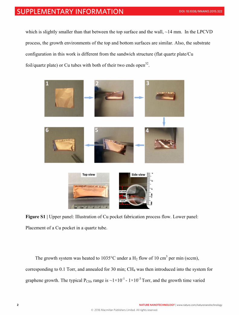
similar growth results. After cleaning, the Cu foils were made into a semi-sealed pocket (Fig. S1)
and then loaded into the quartz tube of a low pressure CVD (LPCVD) system. The pockets were
“sitting” directly in a quartz tube (lower panel of Fig. S1). The typical width of the pocket is
~18mm and the inner diameter of the quartz tube is ~22mm. In this way, when the pocket sits
inside the tube, the distance between the bottom surface and the quartz tube wall is ~7 mm,
Oxygen-activated growth and bandgap tunabilityof large single-crystal bilayer graphene
© 2016 Macmillan Publishers Limited. All rights reserved.
2 NATURE NANOTECHNOLOGY | www.nature.com/naturenanotechnology
SUPPLEMENTARY INFORMATION DOI: 10.1038/NNANO.2015.322
2
which is slightly smaller than that between the top surface and the wall, ~14 mm. In the LPCVD
process, the growth environments of the top and bottom surfaces are similar. Also, the substrate
configuration in this work is different from the sandwich structure (flat quartz plate/Cu
foil/quartz plate) or Cu tubes with both of their two ends open32.
Figure S1 | Upper panel: Illustration of Cu pocket fabrication process flow. Lower panel:
Placement of a Cu pocket in a quartz tube.
The growth system was heated to 1035°C under a H2 flow of 10 cm3 per min (sccm),
corresponding to 0.1 Torr, and annealed for 30 min; CH4 was then introduced into the system for
graphene growth. The typical PCH4 range is ~1×10⁻¹ - 1×10⁻³ Torr, and the growth time varied
3
from 10 to 500 min. Note that for "O2-treated OF-Cu", pure O2 was used for different exposure
time right before introducing CH4 and the corresponding PO2 is 1×10⁻³ Torr. After growth, the
system was cooled down to room temperature while still under the H2 and CH4 flow. The bilayer
and few-layer graphene films formed on the exterior surface of the Cu pockets were
characterized and analyzed.
The graphene domains/films were transferred onto dielectric surfaces, Si and h-BN, using a
poly(methyl methacrylate) (PMMA)-assisted method33 for Raman characterization and electrical
device fabrication. Prior to transfer, the graphene surface was spin-coated with a layer of PMMA
to provide mechanical support throughout the transfer process. The PMMA/graphene/Cu stack
was then floated over an ammonium persulfate ((NH4)2S2O8, 0.5 M, Sigma Aldrich) aqueous
solution to etch the Cu. The resulting graphene/PMMA membranes are thoroughly rinsed with
deionized water, and then transferred onto the target substrates. The PMMA was removed with
acetone, then rinsed in isopropanol, and finally blow-dried with nitrogen gas.
SEM images were taken with an FEI Quanta-600 FEG Environmental SEM with the
accelerating voltage of 30 KV, and spot size of 5. Raman spectra and mapping images were
taken from a WiTec Alpha 300 micro-Raman imaging system. A 488 nm excitation laser with a
50× or 100 × objective lens were used for the acquisition of Raman spectra and images. The spot
size is 200-500 nm, and the mapping step size is ~300nm.
SUPPLEMENTARY NOTES
A. Gas-flow dynamics of Cu pocket and its effects on graphene growth
© 2016 Macmillan Publishers Limited. All rights reserved.
NATURE NANOTECHNOLOGY | www.nature.com/naturenanotechnology 3
SUPPLEMENTARY INFORMATIONDOI: 10.1038/NNANO.2015.322
2
which is slightly smaller than that between the top surface and the wall, ~14 mm. In the LPCVD
process, the growth environments of the top and bottom surfaces are similar. Also, the substrate
configuration in this work is different from the sandwich structure (flat quartz plate/Cu
foil/quartz plate) or Cu tubes with both of their two ends open32.
Figure S1 | Upper panel: Illustration of Cu pocket fabrication process flow. Lower panel:
Placement of a Cu pocket in a quartz tube.
The growth system was heated to 1035°C under a H2 flow of 10 cm3 per min (sccm),
corresponding to 0.1 Torr, and annealed for 30 min; CH4 was then introduced into the system for
graphene growth. The typical PCH4 range is ~1×10⁻¹ - 1×10⁻³ Torr, and the growth time varied
3
from 10 to 500 min. Note that for "O2-treated OF-Cu", pure O2 was used for different exposure
time right before introducing CH4 and the corresponding PO2 is 1×10⁻³ Torr. After growth, the
system was cooled down to room temperature while still under the H2 and CH4 flow. The bilayer
and few-layer graphene films formed on the exterior surface of the Cu pockets were
characterized and analyzed.
The graphene domains/films were transferred onto dielectric surfaces, Si and h-BN, using a
poly(methyl methacrylate) (PMMA)-assisted method33 for Raman characterization and electrical
device fabrication. Prior to transfer, the graphene surface was spin-coated with a layer of PMMA
to provide mechanical support throughout the transfer process. The PMMA/graphene/Cu stack
was then floated over an ammonium persulfate ((NH4)2S2O8, 0.5 M, Sigma Aldrich) aqueous
solution to etch the Cu. The resulting graphene/PMMA membranes are thoroughly rinsed with
deionized water, and then transferred onto the target substrates. The PMMA was removed with
acetone, then rinsed in isopropanol, and finally blow-dried with nitrogen gas.
SEM images were taken with an FEI Quanta-600 FEG Environmental SEM with the
accelerating voltage of 30 KV, and spot size of 5. Raman spectra and mapping images were
taken from a WiTec Alpha 300 micro-Raman imaging system. A 488 nm excitation laser with a
50× or 100 × objective lens were used for the acquisition of Raman spectra and images. The spot
size is 200-500 nm, and the mapping step size is ~300nm.
SUPPLEMENTARY NOTES
A. Gas-flow dynamics of Cu pocket and its effects on graphene growth
© 2016 Macmillan Publishers Limited. All rights reserved.
4 NATURE NANOTECHNOLOGY | www.nature.com/naturenanotechnology
SUPPLEMENTARY INFORMATION DOI: 10.1038/NNANO.2015.322
4
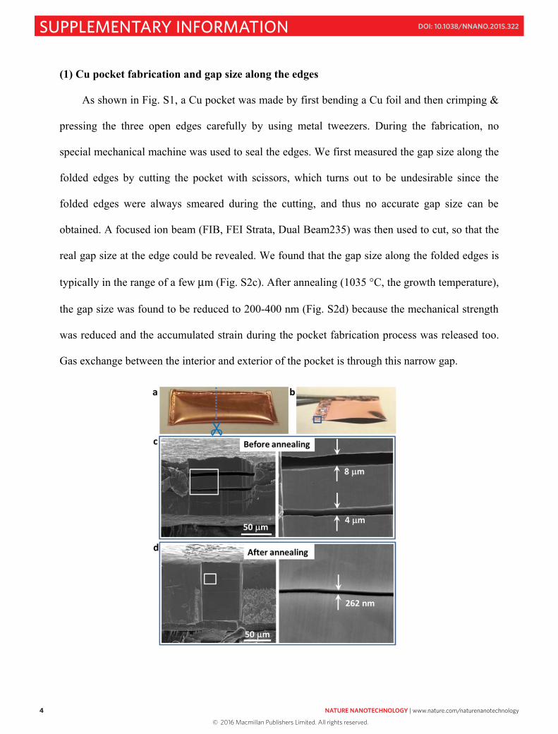
(1) Cu pocket fabrication and gap size along the edges
As shown in Fig. S1, a Cu pocket was made by first bending a Cu foil and then crimping &
pressing the three open edges carefully by using metal tweezers. During the fabrication, no
special mechanical machine was used to seal the edges. We first measured the gap size along the
folded edges by cutting the pocket with scissors, which turns out to be undesirable since the
folded edges were always smeared during the cutting, and thus no accurate gap size can be
obtained. A focused ion beam (FIB, FEI Strata, Dual Beam235) was then used to cut, so that the
real gap size at the edge could be revealed. We found that the gap size along the folded edges is
typically in the range of a few μm (Fig. S2c). After annealing (1035 °C, the growth temperature),
the gap size was found to be reduced to 200-400 nm (Fig. S2d) because the mechanical strength
was reduced and the accumulated strain during the pocket fabrication process was released too.
Gas exchange between the interior and exterior of the pocket is through this narrow gap.
5
Figure S2 | The pocket was cut by scissors first a, and then focused ion beams were used to cut
the local region as indicated by the blue-line box in b. The gap sizes before and after annealing
are shown in c and d, respectively.
(2) Gas equilibrium and Knudsen diffusion
In the experimental environment, where the temperature is above 1000°C and the gas
pressure is ~0.1 Torr, the calculated mean free path of CH4 molecules is larger than 1mm34.
Hence the Knudsen number, which is defined as the ratio of the mean free path of CH4 molecules
to the gap size of the Cu pocket, is on the order of 104. Such a high Knudsen number suggests
that the diffusion of CH4 from the exterior environment into the interior through the gap of the
pocket is dominated by the collisions between CH4 molecules and the gap sidewall, and is in the
Knudsen diffusion regime. The diffusivity in the gap channel (indicated in Fig. S3a) is thus much
lower than the diffusivity outside the Cu pocket.
The diffusivity in the Knudsen diffusion regime depends on both the shape and dimensions
of the channel. Monte Carlo simulation35,36 provides a convenient way to calculate the diffusivity
of CH4 molecules inside the channel of the Cu pocket which is modelled as a nano-channel. In
the simulation, the channel connects two infinitely large reservoirs of which the gas
concentrations (or called number densities) are maintained at constant, but different values.
When the system reaches the steady state, a linear density profile along the length of the channel
is established and the number flux of gas molecules is measured. It is found that in the Knudsen
diffusion regime, the number flux, J, follows the Fick’s first law of diffusion,
dnJ Ddx
=− , (1)
© 2016 Macmillan Publishers Limited. All rights reserved.
NATURE NANOTECHNOLOGY | www.nature.com/naturenanotechnology 5
SUPPLEMENTARY INFORMATIONDOI: 10.1038/NNANO.2015.322
4
(1) Cu pocket fabrication and gap size along the edges
As shown in Fig. S1, a Cu pocket was made by first bending a Cu foil and then crimping &
pressing the three open edges carefully by using metal tweezers. During the fabrication, no
special mechanical machine was used to seal the edges. We first measured the gap size along the
folded edges by cutting the pocket with scissors, which turns out to be undesirable since the
folded edges were always smeared during the cutting, and thus no accurate gap size can be
obtained. A focused ion beam (FIB, FEI Strata, Dual Beam235) was then used to cut, so that the
real gap size at the edge could be revealed. We found that the gap size along the folded edges is
typically in the range of a few μm (Fig. S2c). After annealing (1035 °C, the growth temperature),
the gap size was found to be reduced to 200-400 nm (Fig. S2d) because the mechanical strength
was reduced and the accumulated strain during the pocket fabrication process was released too.
Gas exchange between the interior and exterior of the pocket is through this narrow gap.
5
Figure S2 | The pocket was cut by scissors first a, and then focused ion beams were used to cut
the local region as indicated by the blue-line box in b. The gap sizes before and after annealing
are shown in c and d, respectively.
(2) Gas equilibrium and Knudsen diffusion
In the experimental environment, where the temperature is above 1000°C and the gas
pressure is ~0.1 Torr, the calculated mean free path of CH4 molecules is larger than 1mm34.
Hence the Knudsen number, which is defined as the ratio of the mean free path of CH4 molecules
to the gap size of the Cu pocket, is on the order of 104. Such a high Knudsen number suggests
that the diffusion of CH4 from the exterior environment into the interior through the gap of the
pocket is dominated by the collisions between CH4 molecules and the gap sidewall, and is in the
Knudsen diffusion regime. The diffusivity in the gap channel (indicated in Fig. S3a) is thus much
lower than the diffusivity outside the Cu pocket.
The diffusivity in the Knudsen diffusion regime depends on both the shape and dimensions
of the channel. Monte Carlo simulation35,36 provides a convenient way to calculate the diffusivity
of CH4 molecules inside the channel of the Cu pocket which is modelled as a nano-channel. In
the simulation, the channel connects two infinitely large reservoirs of which the gas
concentrations (or called number densities) are maintained at constant, but different values.
When the system reaches the steady state, a linear density profile along the length of the channel
is established and the number flux of gas molecules is measured. It is found that in the Knudsen
diffusion regime, the number flux, J, follows the Fick’s first law of diffusion,
dnJ Ddx
=− , (1)
© 2016 Macmillan Publishers Limited. All rights reserved.
6 NATURE NANOTECHNOLOGY | www.nature.com/naturenanotechnology
SUPPLEMENTARY INFORMATION DOI: 10.1038/NNANO.2015.322
6
and the diffusivity D can be calculated based on the simulated number flux and the gradient of
number density along the channel, dndx
. Using this method, the diffusivity of CH4 molecules in a
channel with a rectangular cross section of which the dimensions are 400 nm and 8 cm,
respectively, is computed. The result is found to be close to that calculated from the formula for
the diffusivity of gas molecules between two infinitely large parallel plates, which is derived
based on ref. 37,
MTKHD B
p ππ 8
41 Λ= , (2)
where H is the gap size, 400nm, M is the molecular weight, and pΛ a is a pre-factor calculated in
ref. 37.
In our experiments, the channel dimensions are: H = 400 nm, W = 8 cm (the edge length of
a pocket), L = 2 mm (length of gap channel, Fig. S3a), and the volume of the Cu pocket is 2mm3.
The calculated diffusivity inside the channel is: D = 1.05 ×10⁻³ m2/s, which is about 4 orders of
magnitude lower than that outside the pocket, which is in the continuum gas transport regime.
We then calculate the time it takes for the number density (equivalent to PCH4) of CH4
molecules to equilibrate between the interior and the exterior of the pocket. The exterior
environment is modelled as an infinitely large reservoir at , in which the number density of
CH4 molecules is maintained at a constant value . It is connected to the Cu pocket through the
nano-channel with a length L. Assuming a uniformly distributed number density of CH4
molecules in the interior environment of the pocket, the change of the number density of CH4
7
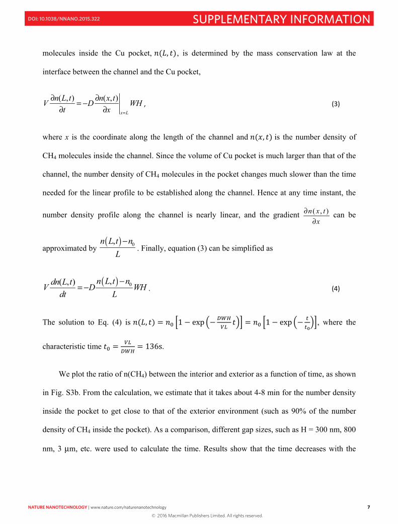
molecules inside the Cu pocket, ���� ��, is determined by the mass conservation law at the
interface between the channel and the Cu pocket,
( , ) ( , )
x L
n L t n x tV D WHt x =
∂ ∂= −∂ ∂
, (3)
where x is the coordinate along the length of the channel and ���� �� is the number density of
CH4 molecules inside the channel. Since the volume of Cu pocket is much larger than that of the
channel, the number density of CH4 molecules in the pocket changes much slower than the time
needed for the linear profile to be established along the channel. Hence at any time instant, the
number density profile along the channel is nearly linear, and the gradient ( , )n x tx
∂∂
can be
approximated by ( ) 0,n L t n
L−
. Finally, equation (3) can be simplified as
( ) 0,( , ) n L t ndn L tV D WHdt L
−= − . (4)
The solution to Eq. (4) is ���� �� = �� �1 � ��� ������� ��� = �� �1 � ��� �� �
����, where the
characteristic time �� = ����� = 136s.
We plot the ratio of n(CH4) between the interior and exterior as a function of time, as shown
in Fig. S3b. From the calculation, we estimate that it takes about 4-8 min for the number density
inside the pocket to get close to that of the exterior environment (such as 90% of the number
density of CH4 inside the pocket). As a comparison, different gap sizes, such as H = 300 nm, 800
nm, 3 μm, etc. were used to calculate the time. Results show that the time decreases with the
© 2016 Macmillan Publishers Limited. All rights reserved.
NATURE NANOTECHNOLOGY | www.nature.com/naturenanotechnology 7
SUPPLEMENTARY INFORMATIONDOI: 10.1038/NNANO.2015.322
6
and the diffusivity D can be calculated based on the simulated number flux and the gradient of
number density along the channel, dndx
. Using this method, the diffusivity of CH4 molecules in a
channel with a rectangular cross section of which the dimensions are 400 nm and 8 cm,
respectively, is computed. The result is found to be close to that calculated from the formula for
the diffusivity of gas molecules between two infinitely large parallel plates, which is derived
based on ref. 37,
MTKHD B
p ππ 8
41 Λ= , (2)
where H is the gap size, 400nm, M is the molecular weight, and pΛ a is a pre-factor calculated in
ref. 37.
In our experiments, the channel dimensions are: H = 400 nm, W = 8 cm (the edge length of
a pocket), L = 2 mm (length of gap channel, Fig. S3a), and the volume of the Cu pocket is 2mm3.
The calculated diffusivity inside the channel is: D = 1.05 ×10⁻³ m2/s, which is about 4 orders of
magnitude lower than that outside the pocket, which is in the continuum gas transport regime.
We then calculate the time it takes for the number density (equivalent to PCH4) of CH4
molecules to equilibrate between the interior and the exterior of the pocket. The exterior
environment is modelled as an infinitely large reservoir at , in which the number density of
CH4 molecules is maintained at a constant value . It is connected to the Cu pocket through the
nano-channel with a length L. Assuming a uniformly distributed number density of CH4
molecules in the interior environment of the pocket, the change of the number density of CH4
7
molecules inside the Cu pocket, ���� ��, is determined by the mass conservation law at the
interface between the channel and the Cu pocket,
( , ) ( , )
x L
n L t n x tV D WHt x =
∂ ∂= −∂ ∂
, (3)
where x is the coordinate along the length of the channel and ���� �� is the number density of
CH4 molecules inside the channel. Since the volume of Cu pocket is much larger than that of the
channel, the number density of CH4 molecules in the pocket changes much slower than the time
needed for the linear profile to be established along the channel. Hence at any time instant, the
number density profile along the channel is nearly linear, and the gradient ( , )n x tx
∂∂
can be
approximated by ( ) 0,n L t n
L−
. Finally, equation (3) can be simplified as
( ) 0,( , ) n L t ndn L tV D WHdt L
−= − . (4)
The solution to Eq. (4) is ���� �� = �� �1 � ��� ������� ��� = �� �1 � ��� �� �
����, where the
characteristic time �� = ����� = 136s.
We plot the ratio of n(CH4) between the interior and exterior as a function of time, as shown
in Fig. S3b. From the calculation, we estimate that it takes about 4-8 min for the number density
inside the pocket to get close to that of the exterior environment (such as 90% of the number
density of CH4 inside the pocket). As a comparison, different gap sizes, such as H = 300 nm, 800
nm, 3 μm, etc. were used to calculate the time. Results show that the time decreases with the
© 2016 Macmillan Publishers Limited. All rights reserved.
8 NATURE NANOTECHNOLOGY | www.nature.com/naturenanotechnology
SUPPLEMENTARY INFORMATION DOI: 10.1038/NNANO.2015.322
8
increased gap size. From the curve in Fig.S3c, the time decreases to a few seconds when the gap
is more than a few μm.
In summary, the narrow gap of a few hundred nm creates a stagnant growth environment in
the interior of the pocket. Significantly low gas exchange rate occurs when the gap size is lower
than about 1 μm. In addition, we are also aware that some CH4 molecules are adsorbed on the Cu
sidewall of the gap channel when diffusing into the pocket, which may further slow-down the
gas exchange.
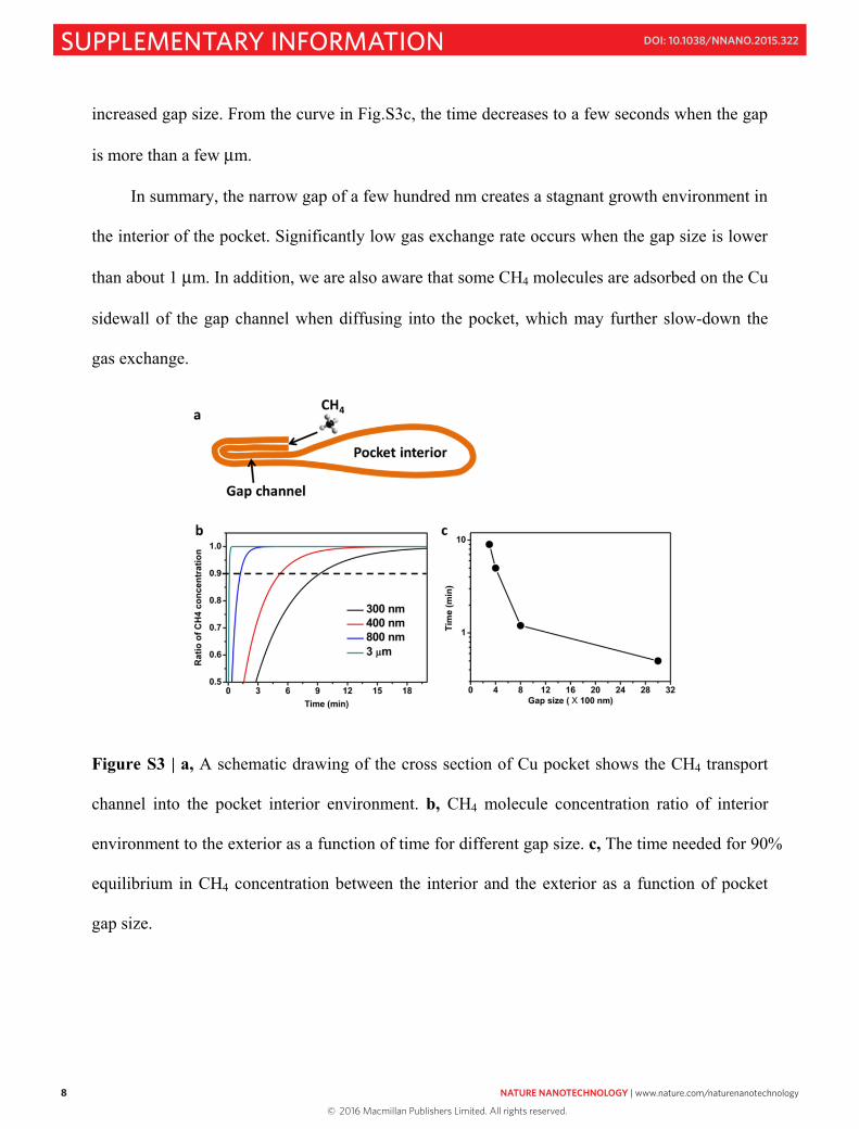
Figure S3 | a, A schematic drawing of the cross section of Cu pocket shows the CH4 transport
channel into the pocket interior environment. b, CH4 molecule concentration ratio of interior
environment to the exterior as a function of time for different gap size. c, The time needed for 90%
equilibrium in CH4 concentration between the interior and the exterior as a function of pocket
gap size.
9
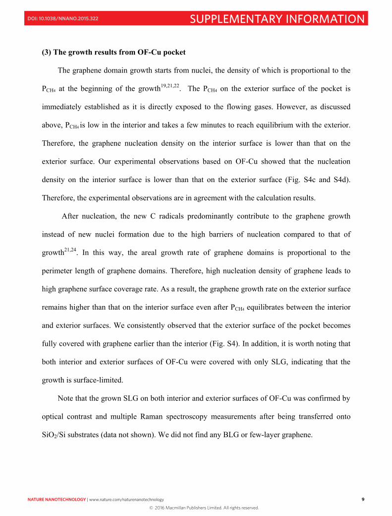
(3) The growth results from OF-Cu pocket
The graphene domain growth starts from nuclei, the density of which is proportional to the
PCH4 at the beginning of the growth19,21,22. The PCH4 on the exterior surface of the pocket is
immediately established as it is directly exposed to the flowing gases. However, as discussed
above, PCH4 is low in the interior and takes a few minutes to reach equilibrium with the exterior.
Therefore, the graphene nucleation density on the interior surface is lower than that on the
exterior surface. Our experimental observations based on OF-Cu showed that the nucleation
density on the interior surface is lower than that on the exterior surface (Fig. S4c and S4d).
Therefore, the experimental observations are in agreement with the calculation results.
After nucleation, the new C radicals predominantly contribute to the graphene growth
instead of new nuclei formation due to the high barriers of nucleation compared to that of
growth21,24. In this way, the areal growth rate of graphene domains is proportional to the
perimeter length of graphene domains. Therefore, high nucleation density of graphene leads to
high graphene surface coverage rate. As a result, the graphene growth rate on the exterior surface
remains higher than that on the interior surface even after PCH4 equilibrates between the interior
and exterior surfaces. We consistently observed that the exterior surface of the pocket becomes
fully covered with graphene earlier than the interior (Fig. S4). In addition, it is worth noting that
both interior and exterior surfaces of OF-Cu were covered with only SLG, indicating that the
growth is surface-limited.
Note that the grown SLG on both interior and exterior surfaces of OF-Cu was confirmed by
optical contrast and multiple Raman spectroscopy measurements after being transferred onto
SiO2/Si substrates (data not shown). We did not find any BLG or few-layer graphene.
© 2016 Macmillan Publishers Limited. All rights reserved.
NATURE NANOTECHNOLOGY | www.nature.com/naturenanotechnology 9
SUPPLEMENTARY INFORMATIONDOI: 10.1038/NNANO.2015.322
8
increased gap size. From the curve in Fig.S3c, the time decreases to a few seconds when the gap
is more than a few μm.
In summary, the narrow gap of a few hundred nm creates a stagnant growth environment in
the interior of the pocket. Significantly low gas exchange rate occurs when the gap size is lower
than about 1 μm. In addition, we are also aware that some CH4 molecules are adsorbed on the Cu
sidewall of the gap channel when diffusing into the pocket, which may further slow-down the
gas exchange.
Figure S3 | a, A schematic drawing of the cross section of Cu pocket shows the CH4 transport
channel into the pocket interior environment. b, CH4 molecule concentration ratio of interior
environment to the exterior as a function of time for different gap size. c, The time needed for 90%
equilibrium in CH4 concentration between the interior and the exterior as a function of pocket
gap size.
9
(3) The growth results from OF-Cu pocket
The graphene domain growth starts from nuclei, the density of which is proportional to the
PCH4 at the beginning of the growth19,21,22. The PCH4 on the exterior surface of the pocket is
immediately established as it is directly exposed to the flowing gases. However, as discussed
above, PCH4 is low in the interior and takes a few minutes to reach equilibrium with the exterior.
Therefore, the graphene nucleation density on the interior surface is lower than that on the
exterior surface. Our experimental observations based on OF-Cu showed that the nucleation
density on the interior surface is lower than that on the exterior surface (Fig. S4c and S4d).
Therefore, the experimental observations are in agreement with the calculation results.
After nucleation, the new C radicals predominantly contribute to the graphene growth
instead of new nuclei formation due to the high barriers of nucleation compared to that of
growth21,24. In this way, the areal growth rate of graphene domains is proportional to the
perimeter length of graphene domains. Therefore, high nucleation density of graphene leads to
high graphene surface coverage rate. As a result, the graphene growth rate on the exterior surface
remains higher than that on the interior surface even after PCH4 equilibrates between the interior
and exterior surfaces. We consistently observed that the exterior surface of the pocket becomes
fully covered with graphene earlier than the interior (Fig. S4). In addition, it is worth noting that
both interior and exterior surfaces of OF-Cu were covered with only SLG, indicating that the
growth is surface-limited.
Note that the grown SLG on both interior and exterior surfaces of OF-Cu was confirmed by
optical contrast and multiple Raman spectroscopy measurements after being transferred onto
SiO2/Si substrates (data not shown). We did not find any BLG or few-layer graphene.
© 2016 Macmillan Publishers Limited. All rights reserved.
10 NATURE NANOTECHNOLOGY | www.nature.com/naturenanotechnology
SUPPLEMENTARY INFORMATION DOI: 10.1038/NNANO.2015.322
10
Figure S4 | The parameter effects on the growth results of graphene on both interior and exterior
surfaces of OF-Cu pockets. T=1035°C, growth time varies in different cases.
B. Experimental study of BLG growth mechanism
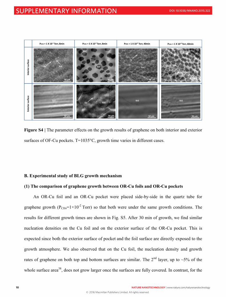
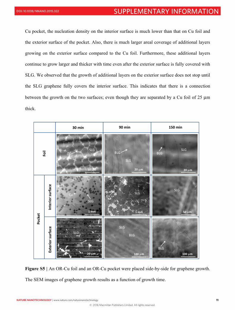
(1) The comparison of graphene growth between OR-Cu foils and OR-Cu pockets
An OR-Cu foil and an OR-Cu pocket were placed side-by-side in the quartz tube for
graphene growth (PCH4=1×10⁻² Torr) so that both were under the same growth conditions. The
results for different growth times are shown in Fig. S5. After 30 min of growth, we find similar
nucleation densities on the Cu foil and on the exterior surface of the OR-Cu pocket. This is
expected since both the exterior surface of pocket and the foil surface are directly exposed to the
growth atmosphere. We also observed that on the Cu foil, the nucleation density and growth
rates of graphene on both top and bottom surfaces are similar. The 2nd layer, up to ~5% of the
whole surface area38, does not grow larger once the surfaces are fully covered. In contrast, for the
11
Cu pocket, the nucleation density on the interior surface is much lower than that on Cu foil and
the exterior surface of the pocket. Also, there is much larger areal coverage of additional layers
growing on the exterior surface compared to the Cu foil. Furthermore, these additional layers
continue to grow larger and thicker with time even after the exterior surface is fully covered with
SLG. We observed that the growth of additional layers on the exterior surface does not stop until
the SLG graphene fully covers the interior surface. This indicates that there is a connection
between the growth on the two surfaces; even though they are separated by a Cu foil of 25 μm
thick.
Figure S5 | An OR-Cu foil and an OR-Cu pocket were placed side-by-side for graphene growth.
The SEM images of graphene growth results as a function of growth time.
© 2016 Macmillan Publishers Limited. All rights reserved.
NATURE NANOTECHNOLOGY | www.nature.com/naturenanotechnology 11
SUPPLEMENTARY INFORMATIONDOI: 10.1038/NNANO.2015.322
10
Figure S4 | The parameter effects on the growth results of graphene on both interior and exterior
surfaces of OF-Cu pockets. T=1035°C, growth time varies in different cases.
B. Experimental study of BLG growth mechanism
(1) The comparison of graphene growth between OR-Cu foils and OR-Cu pockets
An OR-Cu foil and an OR-Cu pocket were placed side-by-side in the quartz tube for
graphene growth (PCH4=1×10⁻² Torr) so that both were under the same growth conditions. The
results for different growth times are shown in Fig. S5. After 30 min of growth, we find similar
nucleation densities on the Cu foil and on the exterior surface of the OR-Cu pocket. This is
expected since both the exterior surface of pocket and the foil surface are directly exposed to the
growth atmosphere. We also observed that on the Cu foil, the nucleation density and growth
rates of graphene on both top and bottom surfaces are similar. The 2nd layer, up to ~5% of the
whole surface area38, does not grow larger once the surfaces are fully covered. In contrast, for the
11
Cu pocket, the nucleation density on the interior surface is much lower than that on Cu foil and
the exterior surface of the pocket. Also, there is much larger areal coverage of additional layers
growing on the exterior surface compared to the Cu foil. Furthermore, these additional layers
continue to grow larger and thicker with time even after the exterior surface is fully covered with
SLG. We observed that the growth of additional layers on the exterior surface does not stop until
the SLG graphene fully covers the interior surface. This indicates that there is a connection
between the growth on the two surfaces; even though they are separated by a Cu foil of 25 μm
thick.
Figure S5 | An OR-Cu foil and an OR-Cu pocket were placed side-by-side for graphene growth.
The SEM images of graphene growth results as a function of growth time.
© 2016 Macmillan Publishers Limited. All rights reserved.
12 NATURE NANOTECHNOLOGY | www.nature.com/naturenanotechnology
SUPPLEMENTARY INFORMATION DOI: 10.1038/NNANO.2015.322
12
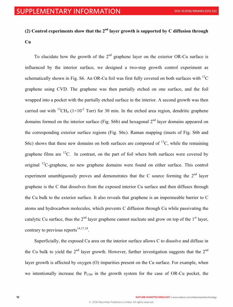
(2) Control experiments show that the 2nd layer growth is supported by C diffusion through
Cu
To elucidate how the growth of the 2nd graphene layer on the exterior OR-Cu surface is
influenced by the interior surface, we designed a two-step growth control experiment as
schematically shown in Fig. S6. An OR-Cu foil was first fully covered on both surfaces with 12C
graphene using CVD. The graphene was then partially etched on one surface, and the foil
wrapped into a pocket with the partially etched surface in the interior. A second growth was then
carried out with 13CH4 (1×10⁻² Torr) for 30 min. In the etched area region, dendritic graphene
domains formed on the interior surface (Fig. S6b) and hexagonal 2nd layer domains appeared on
the corresponding exterior surface regions (Fig. S6c). Raman mapping (insets of Fig. S6b and
S6c) shows that these new domains on both surfaces are composed of 13C, while the remaining
graphene films are 12C. In contrast, on the part of foil where both surfaces were covered by
original 12C-graphene, no new graphene domains were found on either surface. This control
experiment unambiguously proves and demonstrates that the C source forming the 2nd layer
graphene is the C that dissolves from the exposed interior Cu surface and then diffuses through
the Cu bulk to the exterior surface. It also reveals that graphene is an impermeable barrier to C
atoms and hydrocarbon molecules, which prevents C diffusion through Cu while passivating the
catalytic Cu surface, thus the 2nd layer graphene cannot nucleate and grow on top of the 1st layer,
contrary to previous reports14,17,18.
Superficially, the exposed Cu area on the interior surface allows C to dissolve and diffuse in
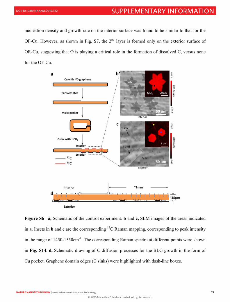
the Cu bulk to yield the 2nd layer growth. However, further investigation suggests that the 2nd
layer growth is affected by oxygen (O) impurities present on the Cu surface. For example, when
we intentionally increase the PCH4 in the growth system for the case of OR-Cu pocket, the
13
nucleation density and growth rate on the interior surface was found to be similar to that for the
OF-Cu. However, as shown in Fig. S7, the 2nd layer is formed only on the exterior surface of
OR-Cu, suggesting that O is playing a critical role in the formation of dissolved C, versus none
for the OF-Cu.
Figure S6 | a, Schematic of the control experiment. b and c, SEM images of the areas indicated
in a. Insets in b and c are the corresponding 13C Raman mapping, corresponding to peak intensity
in the range of 1450-1550cm-1. The corresponding Raman spectra at different points were shown
in Fig. S14. d, Schematic drawing of C diffusion processes for the BLG growth in the form of
Cu pocket. Graphene domain edges (C sinks) were highlighted with dash-line boxes.
© 2016 Macmillan Publishers Limited. All rights reserved.
NATURE NANOTECHNOLOGY | www.nature.com/naturenanotechnology 13
SUPPLEMENTARY INFORMATIONDOI: 10.1038/NNANO.2015.322
12
(2) Control experiments show that the 2nd layer growth is supported by C diffusion through
Cu
To elucidate how the growth of the 2nd graphene layer on the exterior OR-Cu surface is
influenced by the interior surface, we designed a two-step growth control experiment as
schematically shown in Fig. S6. An OR-Cu foil was first fully covered on both surfaces with 12C
graphene using CVD. The graphene was then partially etched on one surface, and the foil
wrapped into a pocket with the partially etched surface in the interior. A second growth was then
carried out with 13CH4 (1×10⁻² Torr) for 30 min. In the etched area region, dendritic graphene
domains formed on the interior surface (Fig. S6b) and hexagonal 2nd layer domains appeared on
the corresponding exterior surface regions (Fig. S6c). Raman mapping (insets of Fig. S6b and
S6c) shows that these new domains on both surfaces are composed of 13C, while the remaining
graphene films are 12C. In contrast, on the part of foil where both surfaces were covered by
original 12C-graphene, no new graphene domains were found on either surface. This control
experiment unambiguously proves and demonstrates that the C source forming the 2nd layer
graphene is the C that dissolves from the exposed interior Cu surface and then diffuses through
the Cu bulk to the exterior surface. It also reveals that graphene is an impermeable barrier to C
atoms and hydrocarbon molecules, which prevents C diffusion through Cu while passivating the
catalytic Cu surface, thus the 2nd layer graphene cannot nucleate and grow on top of the 1st layer,
contrary to previous reports14,17,18.
Superficially, the exposed Cu area on the interior surface allows C to dissolve and diffuse in
the Cu bulk to yield the 2nd layer growth. However, further investigation suggests that the 2nd
layer growth is affected by oxygen (O) impurities present on the Cu surface. For example, when
we intentionally increase the PCH4 in the growth system for the case of OR-Cu pocket, the
13
nucleation density and growth rate on the interior surface was found to be similar to that for the
OF-Cu. However, as shown in Fig. S7, the 2nd layer is formed only on the exterior surface of
OR-Cu, suggesting that O is playing a critical role in the formation of dissolved C, versus none
for the OF-Cu.
Figure S6 | a, Schematic of the control experiment. b and c, SEM images of the areas indicated
in a. Insets in b and c are the corresponding 13C Raman mapping, corresponding to peak intensity
in the range of 1450-1550cm-1. The corresponding Raman spectra at different points were shown
in Fig. S14. d, Schematic drawing of C diffusion processes for the BLG growth in the form of
Cu pocket. Graphene domain edges (C sinks) were highlighted with dash-line boxes.
© 2016 Macmillan Publishers Limited. All rights reserved.
14 NATURE NANOTECHNOLOGY | www.nature.com/naturenanotechnology
SUPPLEMENTARY INFORMATION DOI: 10.1038/NNANO.2015.322
14
Figure S7 | Control experiments. PCH4 for OF-Cu is 1 × 10⁻³Torr, while it is 8 × 10⁻² Torr for
OR-Cu. The surface coverage is similar on both interior surfaces, but only on the exterior surface
of OR-Cu, BLG domains were observed. The growth time is 60 minutes for OF-Cu, and 30
minutes for OR-Cu.
(3) The driving force of C diffusion through the Cu bulk to the exterior surface.
The whole growth process of graphene (both SLG and BLG) is a non-equilibrium process
driven by the much lower energy of C in the graphene phase than that of the C radicals on the Cu
surface, which is independent of the local graphene coverage.
We point out that the driving force for C to diffuse through Cu bulk to the exterior surface
to grow the 2nd graphene layer is the higher C atom (or C radical) concentration on the interior
surface than that on the exterior surface, which is the consequence of higher nucleation density
of 2nd layer on the exterior surface than that of SLG on the interior surface. A schematic drawing
15
(not to scale) regarding the process is shown in Fig. S6d. In our previous work19 on the effect of
oxygen on the nucleation density of graphene on Cu, we showed that the interior surface of the
Cu pocket can be exposed to methane for many hours without nucleating new graphene domains,
but becomes covered with a significant amount of C radicals. Therefore when the exterior
surface is fully covered by 1st layer graphene, the C atoms on the largely exposed interior Cu
surface can diffuse either on the interior surface to the sparse graphene domain edges for their
enlargement, or through the Cu bulk to the exterior surface to grow 2nd layer graphene, with
comparable diffusion energy barriers thanks to the help of oxygen (0.92eV vs. 1eV, Table S1).
The nucleation density of 2nd layer on the exterior surface is higher than that of SLG on the
interior surface (this is a general characteristic, and can be seen in Figure 1b and 1c; Figure S5,
S7, and S11, etc). Correspondingly, on the exterior surface there are more 2nd layer domain edges,
which are sinks for C incorporation into graphene lattice and thus keep the C radical
concentration low. Consequently, more C is driven to diffuse through the Cu bulk to the exterior
surface. Further, because the thickness of the Cu is only 25 μm, much smaller than the separation
between graphene islands on the interior surface (~ mm), one can readily see that a significant
fraction of C atoms will diffuse through the foil to the exterior surface to form the 2nd layer
graphene rather than diffusing to the growing domains on the interior surface.
(4) The C bulk diffusion at the beginning of the growth.
To provide a complete picture of the whole growth process, we comment here on the C
diffusion at the beginning of the growth process. Nucleation and growth of 1st layer graphene
islands on the exterior surface of the OR-Cu pocket quickly proceeds through the well-
established surface-mediated mechanism, similar to the case of Cu foil. It is also possible for the
© 2016 Macmillan Publishers Limited. All rights reserved.
NATURE NANOTECHNOLOGY | www.nature.com/naturenanotechnology 15
SUPPLEMENTARY INFORMATIONDOI: 10.1038/NNANO.2015.322
14
Figure S7 | Control experiments. PCH4 for OF-Cu is 1 × 10⁻³Torr, while it is 8 × 10⁻² Torr for
OR-Cu. The surface coverage is similar on both interior surfaces, but only on the exterior surface
of OR-Cu, BLG domains were observed. The growth time is 60 minutes for OF-Cu, and 30
minutes for OR-Cu.
(3) The driving force of C diffusion through the Cu bulk to the exterior surface.
The whole growth process of graphene (both SLG and BLG) is a non-equilibrium process
driven by the much lower energy of C in the graphene phase than that of the C radicals on the Cu
surface, which is independent of the local graphene coverage.
We point out that the driving force for C to diffuse through Cu bulk to the exterior surface
to grow the 2nd graphene layer is the higher C atom (or C radical) concentration on the interior
surface than that on the exterior surface, which is the consequence of higher nucleation density
of 2nd layer on the exterior surface than that of SLG on the interior surface. A schematic drawing
15
(not to scale) regarding the process is shown in Fig. S6d. In our previous work19 on the effect of
oxygen on the nucleation density of graphene on Cu, we showed that the interior surface of the
Cu pocket can be exposed to methane for many hours without nucleating new graphene domains,
but becomes covered with a significant amount of C radicals. Therefore when the exterior
surface is fully covered by 1st layer graphene, the C atoms on the largely exposed interior Cu
surface can diffuse either on the interior surface to the sparse graphene domain edges for their
enlargement, or through the Cu bulk to the exterior surface to grow 2nd layer graphene, with
comparable diffusion energy barriers thanks to the help of oxygen (0.92eV vs. 1eV, Table S1).
The nucleation density of 2nd layer on the exterior surface is higher than that of SLG on the
interior surface (this is a general characteristic, and can be seen in Figure 1b and 1c; Figure S5,
S7, and S11, etc). Correspondingly, on the exterior surface there are more 2nd layer domain edges,
which are sinks for C incorporation into graphene lattice and thus keep the C radical
concentration low. Consequently, more C is driven to diffuse through the Cu bulk to the exterior
surface. Further, because the thickness of the Cu is only 25 μm, much smaller than the separation
between graphene islands on the interior surface (~ mm), one can readily see that a significant
fraction of C atoms will diffuse through the foil to the exterior surface to form the 2nd layer
graphene rather than diffusing to the growing domains on the interior surface.
(4) The C bulk diffusion at the beginning of the growth.
To provide a complete picture of the whole growth process, we comment here on the C
diffusion at the beginning of the growth process. Nucleation and growth of 1st layer graphene
islands on the exterior surface of the OR-Cu pocket quickly proceeds through the well-
established surface-mediated mechanism, similar to the case of Cu foil. It is also possible for the
© 2016 Macmillan Publishers Limited. All rights reserved.
16 NATURE NANOTECHNOLOGY | www.nature.com/naturenanotechnology
SUPPLEMENTARY INFORMATION DOI: 10.1038/NNANO.2015.322
16
CHx on the exterior surface of the OR-Cu pocket to completely dissociate and dissolve into the
Cu bulk, followed by C diffusion to the interior surface. But such processes will unavoidably
stop after the exterior surface being fully covered by graphene, which grows much faster than on
the interior surface because of the asymmetric growth environment of the Cu pocket.
We note that the bulk diffusion from the interior surface to the exterior surface is a critical
pathway for the large 2nd layer graphene growth, which is one of the main points in this work;
while the diffusion in the reversed direction occurs only at the beginning of growth when the
exterior surface is not fully covered with SLG, and is unimportant for the main claim of this
paper.
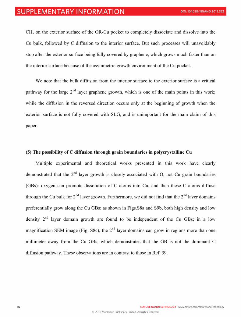
(5) The possibility of C diffusion through grain boundaries in polycrystalline Cu
Multiple experimental and theoretical works presented in this work have clearly
demonstrated that the 2nd layer growth is closely associated with O, not Cu grain boundaries
(GBs): oxygen can promote dissolution of C atoms into Cu, and then these C atoms diffuse
through the Cu bulk for 2nd layer growth. Furthermore, we did not find that the 2nd layer domains
preferentially grow along the Cu GBs: as shown in Figs.S8a and S9b, both high density and low
density 2nd layer domain growth are found to be independent of the Cu GBs; in a low
magnification SEM image (Fig. S8c), the 2nd layer domains can grow in regions more than one
millimeter away from the Cu GBs, which demonstrates that the GB is not the dominant C
diffusion pathway. These observations are in contrast to those in Ref. 39.
17
Figure S8 | The relationship between Cu grain boundaries and 2nd layer growth sites. Note that
in (c) the brightness contrast is due to the non-flatness of Cu surface at large-scale.
(6) Domain shapes: Dendritic versus compact
Different graphene domain shapes are the results of different growth kinetics. In the
previous work 19, we have clearly confirmed that Cu surface O impurities play a critical role in
determining the growth kinetics and hence the domain shapes. So the explanation is as follows:
As grown on the OR-Cu, the 1st layer domains were always dendritic, indicating diffusion-
limited growth. During the growth of the 1st layer, the surface oxygen species were depleted
through the reactions: CHx + O CHx-1 + OH (x=4, 3, 2, 1). Thus the 2nd layer domains were
grown in an oxygen-free environment. The compact domain shapes are a direct consequence of
the edge-attachment-limited growth kinetics in such an environment. This is consistent with our
previous work.
C. Optimization of growth parameters towards larger BLG domains
© 2016 Macmillan Publishers Limited. All rights reserved.
NATURE NANOTECHNOLOGY | www.nature.com/naturenanotechnology 17
SUPPLEMENTARY INFORMATIONDOI: 10.1038/NNANO.2015.322
16
CHx on the exterior surface of the OR-Cu pocket to completely dissociate and dissolve into the
Cu bulk, followed by C diffusion to the interior surface. But such processes will unavoidably
stop after the exterior surface being fully covered by graphene, which grows much faster than on
the interior surface because of the asymmetric growth environment of the Cu pocket.
We note that the bulk diffusion from the interior surface to the exterior surface is a critical
pathway for the large 2nd layer graphene growth, which is one of the main points in this work;
while the diffusion in the reversed direction occurs only at the beginning of growth when the
exterior surface is not fully covered with SLG, and is unimportant for the main claim of this
paper.
(5) The possibility of C diffusion through grain boundaries in polycrystalline Cu
Multiple experimental and theoretical works presented in this work have clearly
demonstrated that the 2nd layer growth is closely associated with O, not Cu grain boundaries
(GBs): oxygen can promote dissolution of C atoms into Cu, and then these C atoms diffuse
through the Cu bulk for 2nd layer growth. Furthermore, we did not find that the 2nd layer domains
preferentially grow along the Cu GBs: as shown in Figs.S8a and S9b, both high density and low
density 2nd layer domain growth are found to be independent of the Cu GBs; in a low
magnification SEM image (Fig. S8c), the 2nd layer domains can grow in regions more than one
millimeter away from the Cu GBs, which demonstrates that the GB is not the dominant C
diffusion pathway. These observations are in contrast to those in Ref. 39.
17
Figure S8 | The relationship between Cu grain boundaries and 2nd layer growth sites. Note that
in (c) the brightness contrast is due to the non-flatness of Cu surface at large-scale.
(6) Domain shapes: Dendritic versus compact
Different graphene domain shapes are the results of different growth kinetics. In the
previous work 19, we have clearly confirmed that Cu surface O impurities play a critical role in
determining the growth kinetics and hence the domain shapes. So the explanation is as follows:
As grown on the OR-Cu, the 1st layer domains were always dendritic, indicating diffusion-
limited growth. During the growth of the 1st layer, the surface oxygen species were depleted
through the reactions: CHx + O CHx-1 + OH (x=4, 3, 2, 1). Thus the 2nd layer domains were
grown in an oxygen-free environment. The compact domain shapes are a direct consequence of
the edge-attachment-limited growth kinetics in such an environment. This is consistent with our
previous work.
C. Optimization of growth parameters towards larger BLG domains
© 2016 Macmillan Publishers Limited. All rights reserved.
18 NATURE NANOTECHNOLOGY | www.nature.com/naturenanotechnology
SUPPLEMENTARY INFORMATION DOI: 10.1038/NNANO.2015.322
18
Since the BLG growth mechanism is established, further efforts were devoted to understand
the effects of various growth parameters so as to achieve larger and more uniform 2nd layer
graphene, while suppressing thicker layer nucleation & growth. In this work, we investigate the
effects of methane partial pressures and O2 pretreatments on BLG growth, and to explore the
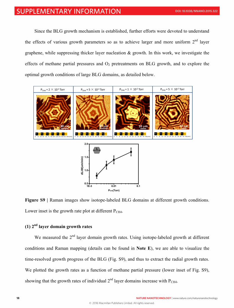
optimal growth conditions of large BLG domains, as detailed below.
Figure S9 | Raman images show isotope-labeled BLG domains at different growth conditions.
Lower inset is the growth rate plot at different PCH4.
(1) 2nd layer domain growth rates
We measured the 2nd layer domain growth rates. Using isotope-labeled growth at different
conditions and Raman mapping (details can be found in Note E), we are able to visualize the
time-resolved growth progress of the BLG (Fig. S9), and thus to extract the radial growth rates.
We plotted the growth rates as a function of methane partial pressure (lower inset of Fig. S9),
showing that the growth rates of individual 2nd layer domains increase with PCH4.
19
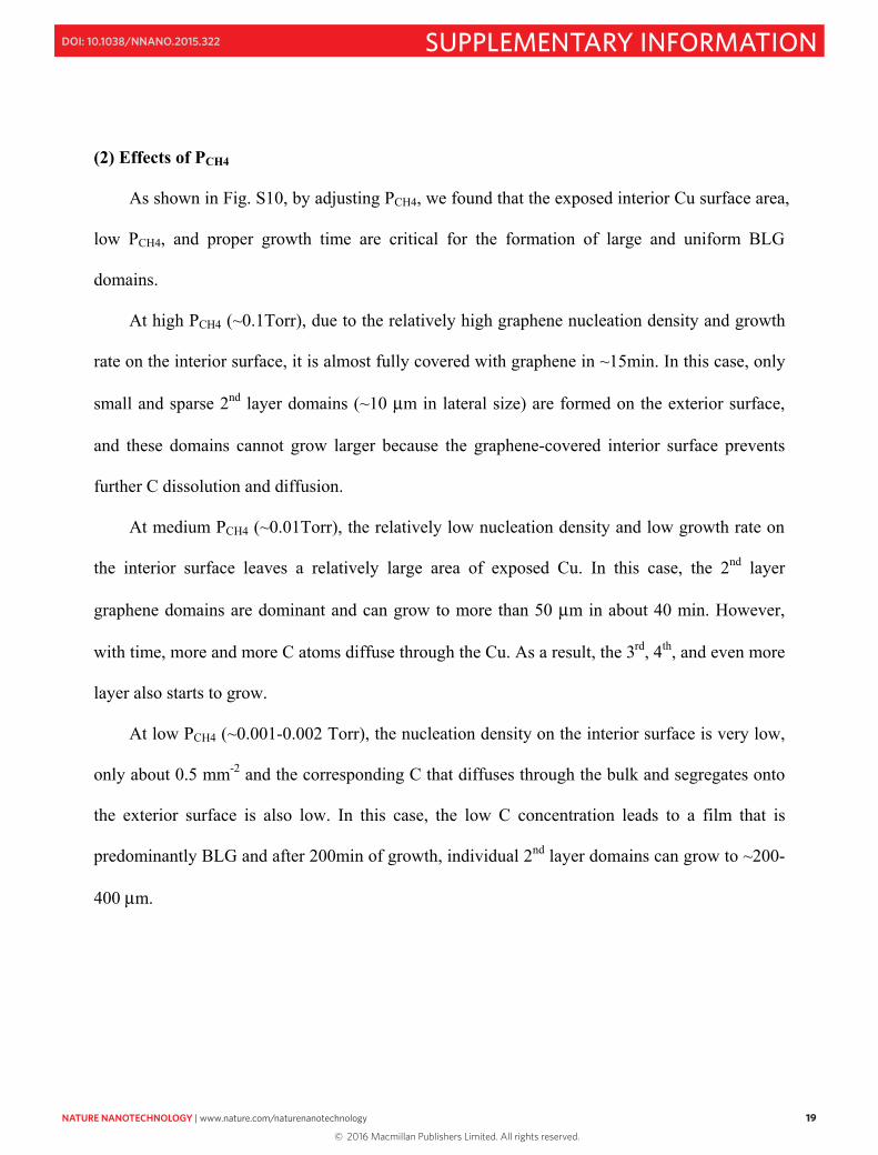
(2) Effects of PCH4
As shown in Fig. S10, by adjusting PCH4, we found that the exposed interior Cu surface area,
low PCH4, and proper growth time are critical for the formation of large and uniform BLG
domains.
At high PCH4 (~0.1Torr), due to the relatively high graphene nucleation density and growth
rate on the interior surface, it is almost fully covered with graphene in ~15min. In this case, only
small and sparse 2nd layer domains (~10 μm in lateral size) are formed on the exterior surface,
and these domains cannot grow larger because the graphene-covered interior surface prevents
further C dissolution and diffusion.
At medium PCH4 (~0.01Torr), the relatively low nucleation density and low growth rate on
the interior surface leaves a relatively large area of exposed Cu. In this case, the 2nd layer
graphene domains are dominant and can grow to more than 50 μm in about 40 min. However,
with time, more and more C atoms diffuse through the Cu. As a result, the 3rd, 4th, and even more
layer also starts to grow.
At low PCH4 (~0.001-0.002 Torr), the nucleation density on the interior surface is very low,
only about 0.5 mm-2 and the corresponding C that diffuses through the bulk and segregates onto
the exterior surface is also low. In this case, the low C concentration leads to a film that is
predominantly BLG and after 200min of growth, individual 2nd layer domains can grow to ~200-
400 μm.
© 2016 Macmillan Publishers Limited. All rights reserved.
NATURE NANOTECHNOLOGY | www.nature.com/naturenanotechnology 19
SUPPLEMENTARY INFORMATIONDOI: 10.1038/NNANO.2015.322
18
Since the BLG growth mechanism is established, further efforts were devoted to understand
the effects of various growth parameters so as to achieve larger and more uniform 2nd layer
graphene, while suppressing thicker layer nucleation & growth. In this work, we investigate the
effects of methane partial pressures and O2 pretreatments on BLG growth, and to explore the
optimal growth conditions of large BLG domains, as detailed below.
Figure S9 | Raman images show isotope-labeled BLG domains at different growth conditions.
Lower inset is the growth rate plot at different PCH4.
(1) 2nd layer domain growth rates
We measured the 2nd layer domain growth rates. Using isotope-labeled growth at different
conditions and Raman mapping (details can be found in Note E), we are able to visualize the
time-resolved growth progress of the BLG (Fig. S9), and thus to extract the radial growth rates.
We plotted the growth rates as a function of methane partial pressure (lower inset of Fig. S9),
showing that the growth rates of individual 2nd layer domains increase with PCH4.
19
(2) Effects of PCH4
As shown in Fig. S10, by adjusting PCH4, we found that the exposed interior Cu surface area,
low PCH4, and proper growth time are critical for the formation of large and uniform BLG
domains.
At high PCH4 (~0.1Torr), due to the relatively high graphene nucleation density and growth
rate on the interior surface, it is almost fully covered with graphene in ~15min. In this case, only
small and sparse 2nd layer domains (~10 μm in lateral size) are formed on the exterior surface,
and these domains cannot grow larger because the graphene-covered interior surface prevents
further C dissolution and diffusion.
At medium PCH4 (~0.01Torr), the relatively low nucleation density and low growth rate on
the interior surface leaves a relatively large area of exposed Cu. In this case, the 2nd layer
graphene domains are dominant and can grow to more than 50 μm in about 40 min. However,
with time, more and more C atoms diffuse through the Cu. As a result, the 3rd, 4th, and even more
layer also starts to grow.
At low PCH4 (~0.001-0.002 Torr), the nucleation density on the interior surface is very low,
only about 0.5 mm-2 and the corresponding C that diffuses through the bulk and segregates onto
the exterior surface is also low. In this case, the low C concentration leads to a film that is
predominantly BLG and after 200min of growth, individual 2nd layer domains can grow to ~200-
400 μm.
© 2016 Macmillan Publishers Limited. All rights reserved.
20 NATURE NANOTECHNOLOGY | www.nature.com/naturenanotechnology
SUPPLEMENTARY INFORMATION DOI: 10.1038/NNANO.2015.322
20
Figure S10 | SEM images of graphene or BLG grown on surfaces of Cu pockets, showing the
effects of methane partial pressure.
21
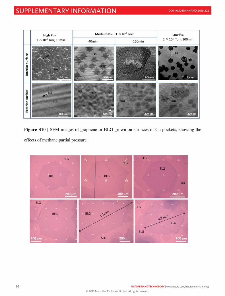
Figure S11 | Optical images of large BLG domains and continuous films on SiO2/Si substrates.
We demonstrate that at low PCH4 and after appropriate growth time, large area BLG and trilayer
graphene can be achieved.
Fig. S11 shows the optical images of individual domains and continuous films of large BLG
and trilayer graphene (TLG) after being transferred onto Si substrates, which were grown at
PCH4=0.001Torr and different growth time.
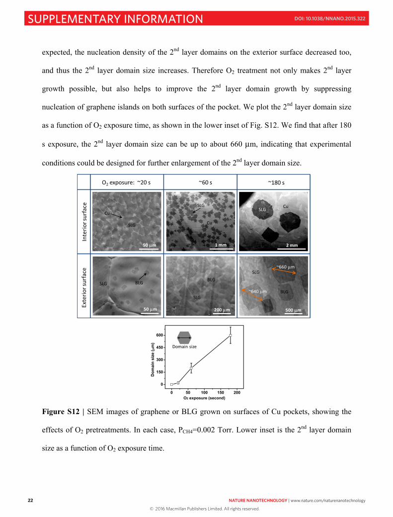
(3) Effects of O2 pretreatments
In this experimental comparison, we treat the OF-Cu substrates with O2 at PO2 = 1×10⁻³ Torr
for different exposure time ranging from 20 s to 5 min. During growth the PCH4 was fixed at
2×10⁻³ Torr in each case. The results are shown in Fig. S12.
On the exterior surface of OF-Cu pockets, we do not observe any BLG growth for a wide
range of growth parameters. However, once small amount of O2 are introduced, say ~20 s before
feeding CH4, we immediately note a change in the growth behavior: on the interior surface, the
graphene domain shape becomes fractal, distinct from the compact domains on pristine OF-Cu,
in agreement with our previous work on SLG. On the exterior surface, we observed low density
2nd layer domains with average size of about 10 μm. Obviously, this is the effect of oxygen
activating the BLG growth as reported in this work. We also note that with the short O2 exposure,
the 2nd layer domains do not grow larger than about 10 μm since the interior surface becomes
fully covered with graphene in about 20 min.
When the O2 exposure time increases, i.e., the surface oxygen concentration increases prior
to growth, the nucleation density of graphene domains on the interior surface decreases as
© 2016 Macmillan Publishers Limited. All rights reserved.
NATURE NANOTECHNOLOGY | www.nature.com/naturenanotechnology 21
SUPPLEMENTARY INFORMATIONDOI: 10.1038/NNANO.2015.322
20
Figure S10 | SEM images of graphene or BLG grown on surfaces of Cu pockets, showing the
effects of methane partial pressure.
21
Figure S11 | Optical images of large BLG domains and continuous films on SiO2/Si substrates.
We demonstrate that at low PCH4 and after appropriate growth time, large area BLG and trilayer
graphene can be achieved.
Fig. S11 shows the optical images of individual domains and continuous films of large BLG
and trilayer graphene (TLG) after being transferred onto Si substrates, which were grown at
PCH4=0.001Torr and different growth time.
(3) Effects of O2 pretreatments
In this experimental comparison, we treat the OF-Cu substrates with O2 at PO2 = 1×10⁻³ Torr
for different exposure time ranging from 20 s to 5 min. During growth the PCH4 was fixed at
2×10⁻³ Torr in each case. The results are shown in Fig. S12.
On the exterior surface of OF-Cu pockets, we do not observe any BLG growth for a wide
range of growth parameters. However, once small amount of O2 are introduced, say ~20 s before
feeding CH4, we immediately note a change in the growth behavior: on the interior surface, the
graphene domain shape becomes fractal, distinct from the compact domains on pristine OF-Cu,
in agreement with our previous work on SLG. On the exterior surface, we observed low density
2nd layer domains with average size of about 10 μm. Obviously, this is the effect of oxygen
activating the BLG growth as reported in this work. We also note that with the short O2 exposure,
the 2nd layer domains do not grow larger than about 10 μm since the interior surface becomes
fully covered with graphene in about 20 min.
When the O2 exposure time increases, i.e., the surface oxygen concentration increases prior
to growth, the nucleation density of graphene domains on the interior surface decreases as
© 2016 Macmillan Publishers Limited. All rights reserved.
22 NATURE NANOTECHNOLOGY | www.nature.com/naturenanotechnology
SUPPLEMENTARY INFORMATION DOI: 10.1038/NNANO.2015.322
22
expected, the nucleation density of the 2nd layer domains on the exterior surface decreased too,
and thus the 2nd layer domain size increases. Therefore O2 treatment not only makes 2nd layer
growth possible, but also helps to improve the 2nd layer domain growth by suppressing
nucleation of graphene islands on both surfaces of the pocket. We plot the 2nd layer domain size
as a function of O2 exposure time, as shown in the lower inset of Fig. S12. We find that after 180
s exposure, the 2nd layer domain size can be up to about 660 μm, indicating that experimental
conditions could be designed for further enlargement of the 2nd layer domain size.
Figure S12 | SEM images of graphene or BLG grown on surfaces of Cu pockets, showing the
effects of O2 pretreatments. In each case, PCH4=0.002 Torr. Lower inset is the 2nd layer domain
size as a function of O2 exposure time.
23
We are aware that other growth parameters, such as PH2, Cu foil thickness, growth time,
growth temperature, etc., may also affect the 2nd layer growth. By tuning the combination of
different parameters, we expect that further improvement in the growth of BLG can be achieved.
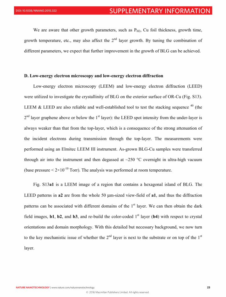
D. Low-energy electron microscopy and low-energy electron diffraction
Low-energy electron microscopy (LEEM) and low-energy electron diffraction (LEED)
were utilized to investigate the crystallinity of BLG on the exterior surface of OR-Cu (Fig. S13).
LEEM & LEED are also reliable and well-established tool to test the stacking sequence 40 (the
2nd layer graphene above or below the 1st layer): the LEED spot intensity from the under-layer is
always weaker than that from the top-layer, which is a consequence of the strong attenuation of
the incident electrons during transmission through the top-layer. The measurements were
performed using an Elmitec LEEM III instrument. As-grown BLG-Cu samples were transferred
through air into the instrument and then degassed at ~250 °C overnight in ultra-high vacuum
(base pressure < 2×10⁻¹⁰ Torr). The analysis was performed at room temperature.
Fig. S13a1 is a LEEM image of a region that contains a hexagonal island of BLG. The
LEED patterns in a2 are from the whole 50 μm-sized view-field of a1, and thus the diffraction
patterns can be associated with different domains of the 1st layer. We can then obtain the dark
field images, b1, b2, and b3, and re-build the color-coded 1st layer (b4) with respect to crystal
orientations and domain morphology. With this detailed but necessary background, we now turn
to the key mechanistic issue of whether the 2nd layer is next to the substrate or on top of the 1st
layer.
© 2016 Macmillan Publishers Limited. All rights reserved.
NATURE NANOTECHNOLOGY | www.nature.com/naturenanotechnology 23
SUPPLEMENTARY INFORMATIONDOI: 10.1038/NNANO.2015.322
22
expected, the nucleation density of the 2nd layer domains on the exterior surface decreased too,
and thus the 2nd layer domain size increases. Therefore O2 treatment not only makes 2nd layer
growth possible, but also helps to improve the 2nd layer domain growth by suppressing
nucleation of graphene islands on both surfaces of the pocket. We plot the 2nd layer domain size
as a function of O2 exposure time, as shown in the lower inset of Fig. S12. We find that after 180
s exposure, the 2nd layer domain size can be up to about 660 μm, indicating that experimental
conditions could be designed for further enlargement of the 2nd layer domain size.
Figure S12 | SEM images of graphene or BLG grown on surfaces of Cu pockets, showing the
effects of O2 pretreatments. In each case, PCH4=0.002 Torr. Lower inset is the 2nd layer domain
size as a function of O2 exposure time.
23
We are aware that other growth parameters, such as PH2, Cu foil thickness, growth time,
growth temperature, etc., may also affect the 2nd layer growth. By tuning the combination of
different parameters, we expect that further improvement in the growth of BLG can be achieved.
D. Low-energy electron microscopy and low-energy electron diffraction
Low-energy electron microscopy (LEEM) and low-energy electron diffraction (LEED)
were utilized to investigate the crystallinity of BLG on the exterior surface of OR-Cu (Fig. S13).
LEEM & LEED are also reliable and well-established tool to test the stacking sequence 40 (the
2nd layer graphene above or below the 1st layer): the LEED spot intensity from the under-layer is
always weaker than that from the top-layer, which is a consequence of the strong attenuation of
the incident electrons during transmission through the top-layer. The measurements were
performed using an Elmitec LEEM III instrument. As-grown BLG-Cu samples were transferred
through air into the instrument and then degassed at ~250 °C overnight in ultra-high vacuum
(base pressure < 2×10⁻¹⁰ Torr). The analysis was performed at room temperature.
Fig. S13a1 is a LEEM image of a region that contains a hexagonal island of BLG. The
LEED patterns in a2 are from the whole 50 μm-sized view-field of a1, and thus the diffraction
patterns can be associated with different domains of the 1st layer. We can then obtain the dark
field images, b1, b2, and b3, and re-build the color-coded 1st layer (b4) with respect to crystal
orientations and domain morphology. With this detailed but necessary background, we now turn
to the key mechanistic issue of whether the 2nd layer is next to the substrate or on top of the 1st
layer.
© 2016 Macmillan Publishers Limited. All rights reserved.
24 NATURE NANOTECHNOLOGY | www.nature.com/naturenanotechnology
SUPPLEMENTARY INFORMATION DOI: 10.1038/NNANO.2015.322
24
Figure S13 | a, LEEM image and the corresponding LEED patterns of a BLG region. The
electron energy is 3.2eV and 50eV for a1 and a2, respectively. b, Dark-field images obtained
from the three sets of diffraction spots in a2, as indicated by red, green, and blue rings. b4, Map
of the 1st layer domains. The three colors represent domains with three different in-plane
rotational orientations of the 1st layer, as revealed by the dark-field LEEM images. The electron
energy is 50eV for b1 to b3. Un-colored 1st layer domains have a different, uncharacterized in-
plane rotation. c, Select-area LEED patterns taken from different regions (2 μm size) in a1, and
the electron energy is 50 eV for each pattern in c. Note that the additional diffraction spots in
each diffraction pattern result from the faceted Cu substrate. The Lower inset schematically
shows the cross-section of this region, where different colors refer to different orientations of
each domain.
25
Distinct from a2, the patterns in c1-c4 are from 2 μm regions, as indicated in a1 and the
schematic drawing in the lower inset. From single-layer regions, c1 and c4 show one set of
strong patterns, while c2 and c3 show two sets of patterns, respectively, since they are taken
from bilayer regions. After comparison with domain morphology (b4) and diffraction pattern
orientations (red spots in c1 and c2; blue spots in c3 and c4), we are able to confirm the red- and
blue-coded spots are from 1st layer and the green-coded spots from the 2nd layer. The consistent
and clear comparisons in each pattern can exclude any artifacts. We then compare the diffraction
spot intensities between the 1st and the 2nd layers and thus conclude the 2nd layer (with weaker
intensity spots) is below the 1st layer.
In addition, we note that the (weak) diffraction spots of the 2nd layer graphene had the same
rotational alignment at all points examined in the hexagonal domain. This indicates that the
hexagonal 2nd layer is a single crystal, a general result found in our analysis of discrete 2nd layer
domains. In addition, by comparing the 2nd layer domain shape with the corresponding
diffraction pattern orientations, the 2nd layer domains were found to be zigzag-edge-terminated,
in accord with previous reports of hexagonal SLG domains on Cu4,19.
E. BLG characterizations using Raman spectroscopy and TEM
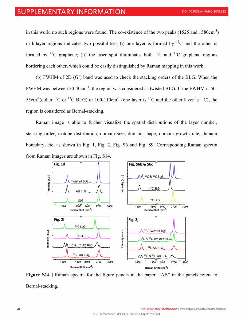
(1) Raman spectroscopy characterizations
Raman spectroscopy was used to study the characteristics of BLG and isotope-labeled BLG
6, 20, 23, 26, 41. Two well-established criteria were used to judge the characteristics of the BLG:
(a) G band positions were used to determine the C isotope-labeling of the graphene regions.
The peak at ~1580 cm-1 indicates 12C graphene, and ~1525cm-1 indicates 13C. If the peak is
between 1525 and 1580cm-1, such as at ~1550cm-1, the film being mixed with both 12C and 13C;
© 2016 Macmillan Publishers Limited. All rights reserved.
NATURE NANOTECHNOLOGY | www.nature.com/naturenanotechnology 25
SUPPLEMENTARY INFORMATIONDOI: 10.1038/NNANO.2015.322
24
Figure S13 | a, LEEM image and the corresponding LEED patterns of a BLG region. The
electron energy is 3.2eV and 50eV for a1 and a2, respectively. b, Dark-field images obtained
from the three sets of diffraction spots in a2, as indicated by red, green, and blue rings. b4, Map
of the 1st layer domains. The three colors represent domains with three different in-plane
rotational orientations of the 1st layer, as revealed by the dark-field LEEM images. The electron
energy is 50eV for b1 to b3. Un-colored 1st layer domains have a different, uncharacterized in-
plane rotation. c, Select-area LEED patterns taken from different regions (2 μm size) in a1, and
the electron energy is 50 eV for each pattern in c. Note that the additional diffraction spots in
each diffraction pattern result from the faceted Cu substrate. The Lower inset schematically
shows the cross-section of this region, where different colors refer to different orientations of
each domain.
25
Distinct from a2, the patterns in c1-c4 are from 2 μm regions, as indicated in a1 and the
schematic drawing in the lower inset. From single-layer regions, c1 and c4 show one set of
strong patterns, while c2 and c3 show two sets of patterns, respectively, since they are taken
from bilayer regions. After comparison with domain morphology (b4) and diffraction pattern
orientations (red spots in c1 and c2; blue spots in c3 and c4), we are able to confirm the red- and
blue-coded spots are from 1st layer and the green-coded spots from the 2nd layer. The consistent
and clear comparisons in each pattern can exclude any artifacts. We then compare the diffraction
spot intensities between the 1st and the 2nd layers and thus conclude the 2nd layer (with weaker
intensity spots) is below the 1st layer.
In addition, we note that the (weak) diffraction spots of the 2nd layer graphene had the same
rotational alignment at all points examined in the hexagonal domain. This indicates that the
hexagonal 2nd layer is a single crystal, a general result found in our analysis of discrete 2nd layer
domains. In addition, by comparing the 2nd layer domain shape with the corresponding
diffraction pattern orientations, the 2nd layer domains were found to be zigzag-edge-terminated,
in accord with previous reports of hexagonal SLG domains on Cu4,19.
E. BLG characterizations using Raman spectroscopy and TEM
(1) Raman spectroscopy characterizations
Raman spectroscopy was used to study the characteristics of BLG and isotope-labeled BLG
6, 20, 23, 26, 41. Two well-established criteria were used to judge the characteristics of the BLG:
(a) G band positions were used to determine the C isotope-labeling of the graphene regions.
The peak at ~1580 cm-1 indicates 12C graphene, and ~1525cm-1 indicates 13C. If the peak is
between 1525 and 1580cm-1, such as at ~1550cm-1, the film being mixed with both 12C and 13C;
© 2016 Macmillan Publishers Limited. All rights reserved.
26 NATURE NANOTECHNOLOGY | www.nature.com/naturenanotechnology
SUPPLEMENTARY INFORMATION DOI: 10.1038/NNANO.2015.322
26
in this work, no such regions were found. The co-existence of the two peaks (1525 and 1580cm-1)
in bilayer regions indicates two possibilities: (i) one layer is formed by 12C and the other is
formed by 13C graphene; (ii) the laser spot illuminates both 12C and 13C graphene regions
bordering each other, which could be easily distinguished by Raman mapping in this work.
(b) FWHM of 2D (G’) band was used to check the stacking orders of the BLG. When the
FWHM was between 20-40cm-1, the region was considered as twisted BLG. If the FWHM is 50-
55cm-1(either 12C or 13C BLG) or 100-110cm-1 (one layer is 12C and the other layer is 13C), the
region is considered as Bernal-stacking.
Raman image is able to further visualize the spatial distributions of the layer number,
stacking order, isotope distribution, domain size, domain shape, domain growth rate, domain
boundary, etc, as shown in Fig. 1, Fig. 2, Fig. S6 and Fig. S9. Corresponding Raman spectra
from Raman images are shown in Fig. S14.
Figure S14 | Raman spectra for the figure panels in the paper. “AB” in the panels refers to
Bernal-stacking.
27
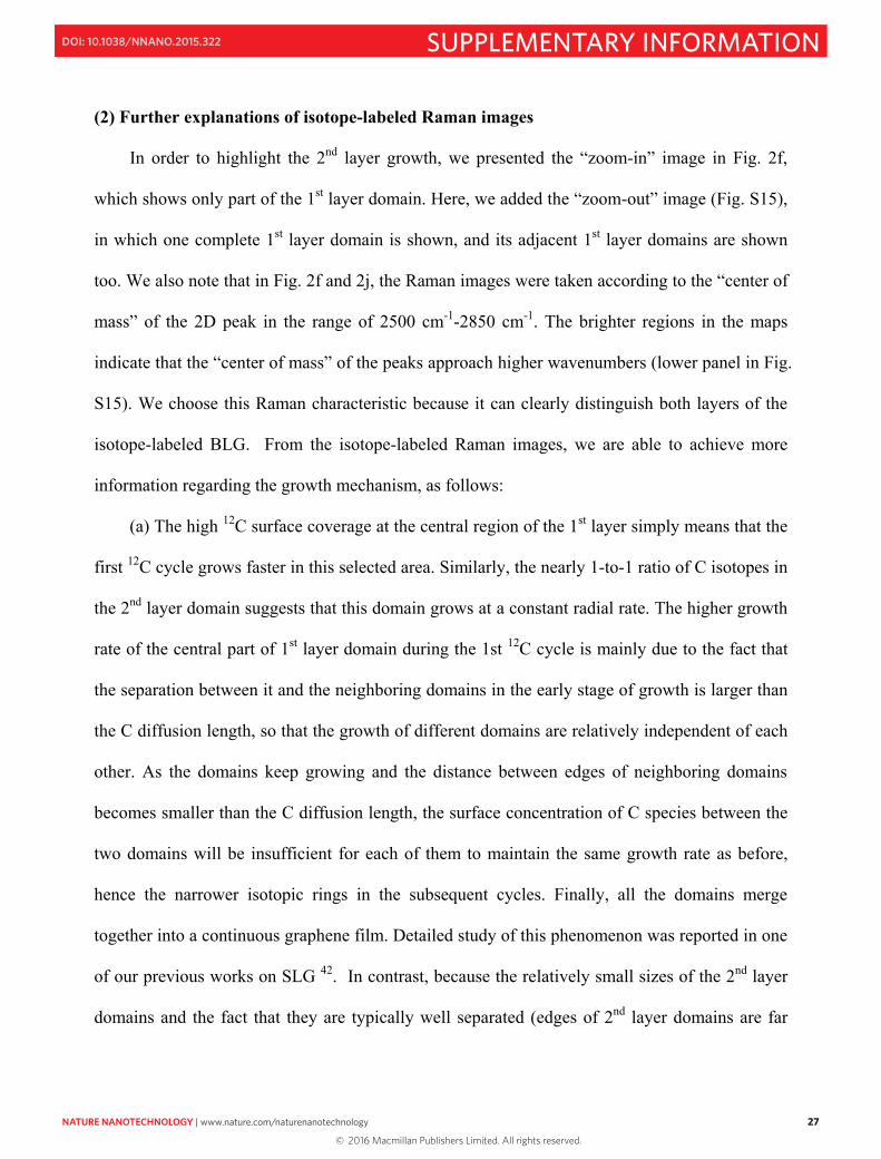
(2) Further explanations of isotope-labeled Raman images
In order to highlight the 2nd layer growth, we presented the “zoom-in” image in Fig. 2f,
which shows only part of the 1st layer domain. Here, we added the “zoom-out” image (Fig. S15),
in which one complete 1st layer domain is shown, and its adjacent 1st layer domains are shown
too. We also note that in Fig. 2f and 2j, the Raman images were taken according to the “center of
mass” of the 2D peak in the range of 2500 cm-1-2850 cm-1. The brighter regions in the maps
indicate that the “center of mass” of the peaks approach higher wavenumbers (lower panel in Fig.
S15). We choose this Raman characteristic because it can clearly distinguish both layers of the
isotope-labeled BLG. From the isotope-labeled Raman images, we are able to achieve more
information regarding the growth mechanism, as follows:
(a) The high 12C surface coverage at the central region of the 1st layer simply means that the
first 12C cycle grows faster in this selected area. Similarly, the nearly 1-to-1 ratio of C isotopes in
the 2nd layer domain suggests that this domain grows at a constant radial rate. The higher growth
rate of the central part of 1st layer domain during the 1st 12C cycle is mainly due to the fact that
the separation between it and the neighboring domains in the early stage of growth is larger than
the C diffusion length, so that the growth of different domains are relatively independent of each
other. As the domains keep growing and the distance between edges of neighboring domains
becomes smaller than the C diffusion length, the surface concentration of C species between the
two domains will be insufficient for each of them to maintain the same growth rate as before,
hence the narrower isotopic rings in the subsequent cycles. Finally, all the domains merge
together into a continuous graphene film. Detailed study of this phenomenon was reported in one
of our previous works on SLG 42. In contrast, because the relatively small sizes of the 2nd layer
domains and the fact that they are typically well separated (edges of 2nd layer domains are far
© 2016 Macmillan Publishers Limited. All rights reserved.
NATURE NANOTECHNOLOGY | www.nature.com/naturenanotechnology 27
SUPPLEMENTARY INFORMATIONDOI: 10.1038/NNANO.2015.322
26
in this work, no such regions were found. The co-existence of the two peaks (1525 and 1580cm-1)
in bilayer regions indicates two possibilities: (i) one layer is formed by 12C and the other is
formed by 13C graphene; (ii) the laser spot illuminates both 12C and 13C graphene regions
bordering each other, which could be easily distinguished by Raman mapping in this work.
(b) FWHM of 2D (G’) band was used to check the stacking orders of the BLG. When the
FWHM was between 20-40cm-1, the region was considered as twisted BLG. If the FWHM is 50-
55cm-1(either 12C or 13C BLG) or 100-110cm-1 (one layer is 12C and the other layer is 13C), the
region is considered as Bernal-stacking.
Raman image is able to further visualize the spatial distributions of the layer number,
stacking order, isotope distribution, domain size, domain shape, domain growth rate, domain
boundary, etc, as shown in Fig. 1, Fig. 2, Fig. S6 and Fig. S9. Corresponding Raman spectra
from Raman images are shown in Fig. S14.
Figure S14 | Raman spectra for the figure panels in the paper. “AB” in the panels refers to
Bernal-stacking.
27
(2) Further explanations of isotope-labeled Raman images
In order to highlight the 2nd layer growth, we presented the “zoom-in” image in Fig. 2f,
which shows only part of the 1st layer domain. Here, we added the “zoom-out” image (Fig. S15),
in which one complete 1st layer domain is shown, and its adjacent 1st layer domains are shown
too. We also note that in Fig. 2f and 2j, the Raman images were taken according to the “center of
mass” of the 2D peak in the range of 2500 cm-1-2850 cm-1. The brighter regions in the maps
indicate that the “center of mass” of the peaks approach higher wavenumbers (lower panel in Fig.
S15). We choose this Raman characteristic because it can clearly distinguish both layers of the
isotope-labeled BLG. From the isotope-labeled Raman images, we are able to achieve more
information regarding the growth mechanism, as follows:
(a) The high 12C surface coverage at the central region of the 1st layer simply means that the
first 12C cycle grows faster in this selected area. Similarly, the nearly 1-to-1 ratio of C isotopes in
the 2nd layer domain suggests that this domain grows at a constant radial rate. The higher growth
rate of the central part of 1st layer domain during the 1st 12C cycle is mainly due to the fact that
the separation between it and the neighboring domains in the early stage of growth is larger than
the C diffusion length, so that the growth of different domains are relatively independent of each
other. As the domains keep growing and the distance between edges of neighboring domains
becomes smaller than the C diffusion length, the surface concentration of C species between the
two domains will be insufficient for each of them to maintain the same growth rate as before,
hence the narrower isotopic rings in the subsequent cycles. Finally, all the domains merge
together into a continuous graphene film. Detailed study of this phenomenon was reported in one
of our previous works on SLG 42. In contrast, because the relatively small sizes of the 2nd layer
domains and the fact that they are typically well separated (edges of 2nd layer domains are far
© 2016 Macmillan Publishers Limited. All rights reserved.
28 NATURE NANOTECHNOLOGY | www.nature.com/naturenanotechnology
SUPPLEMENTARY INFORMATION DOI: 10.1038/NNANO.2015.322
28
from edges of other 2nd layer domains), they maintain a constant radial growth rate as indicated
by the equal widths of the isotopic rings.
(b) Further, we observe that after the first 6-7 isotope cycles (105 minutes of growth time),
the 1st layer domains on the exterior surface merge with adjacent domains and fully cover the Cu
surface. However, because of a lower growth rate, the 2nd layer domains continue to grow up to
12 cycles (180 minutes growth). The difference in growth kinetics for the two layers clearly
shows that the enlargement of the 2nd layer domains is not restricted by the full coverage of the
1st layer graphene on the exterior Cu surface. This further suggests that the 2nd layer growth is
supported by the C bulk diffusion from the interior surface.
29
Figure S15 | “Zoom-out” Raman image of Figure 2f. The growth progress of the whole domains
of both layers was shown, and the grain boundary of the 1st layer film is shown too. Note that
this image was taken according to the “center of mass” of 2D peaks, and the corresponding
Raman spectra at different regions were shown in the lower-right panel.
(c) “Sharp isotope labeled 2nd layer graphene”. In our previous work 23, the contrasting
features between the isotope-labeled graphene films on Ni and on Cu strongly suggest that the
extremely low C solubility in Cu restricts the whole growth processes, such as nucleation and
diffusion, to happening only at surface. We emphasize that those samples were grown in the
conventional geometry (i.e. same conditions on both sides of the Cu foil, such that there is no net
flux of C through the foil). In contrast, in current work we intentionally utilize the asymmetric
growth environment with a Cu pocket to promote the isothermal growth of the 2nd layer. Multiple
control experiments confirmed that small amounts of C can diffuse through the Cu bulk and
segregate onto the exterior surface for the 2nd layer growth. Interestingly, we found the similar
isotopic rings. This appears to be different from the previous case. Here we revisit the scenario,
and found that the occurrence of isotope rings are the results of extremely low C solubility,
efficient diffusion both in bulk and along the interface between Cu and the 1st graphene layer.
We note that significant isotope mixing requires that there is a C reservoir in the bulk of the
metal substrate, i.e. the number of C atoms in the substrate bulk exceeds that in the graphene
grown on it.23 However, the C solubility in Cu is extremely low, so that even if there is mixing
between 12C and 13C dissolved in the Cu foil, the amount is too small to give an obvious isotope-
mixing contrast from that of pure 12C or 13C regions. In other words, the total number of C atoms
passing through the Cu foil and forming graphene on the exterior surface during one isotope
© 2016 Macmillan Publishers Limited. All rights reserved.
NATURE NANOTECHNOLOGY | www.nature.com/naturenanotechnology 29
SUPPLEMENTARY INFORMATIONDOI: 10.1038/NNANO.2015.322
28
from edges of other 2nd layer domains), they maintain a constant radial growth rate as indicated
by the equal widths of the isotopic rings.
(b) Further, we observe that after the first 6-7 isotope cycles (105 minutes of growth time),
the 1st layer domains on the exterior surface merge with adjacent domains and fully cover the Cu
surface. However, because of a lower growth rate, the 2nd layer domains continue to grow up to
12 cycles (180 minutes growth). The difference in growth kinetics for the two layers clearly
shows that the enlargement of the 2nd layer domains is not restricted by the full coverage of the
1st layer graphene on the exterior Cu surface. This further suggests that the 2nd layer growth is
supported by the C bulk diffusion from the interior surface.
29
Figure S15 | “Zoom-out” Raman image of Figure 2f. The growth progress of the whole domains
of both layers was shown, and the grain boundary of the 1st layer film is shown too. Note that
this image was taken according to the “center of mass” of 2D peaks, and the corresponding
Raman spectra at different regions were shown in the lower-right panel.
(c) “Sharp isotope labeled 2nd layer graphene”. In our previous work 23, the contrasting
features between the isotope-labeled graphene films on Ni and on Cu strongly suggest that the
extremely low C solubility in Cu restricts the whole growth processes, such as nucleation and
diffusion, to happening only at surface. We emphasize that those samples were grown in the
conventional geometry (i.e. same conditions on both sides of the Cu foil, such that there is no net
flux of C through the foil). In contrast, in current work we intentionally utilize the asymmetric
growth environment with a Cu pocket to promote the isothermal growth of the 2nd layer. Multiple
control experiments confirmed that small amounts of C can diffuse through the Cu bulk and
segregate onto the exterior surface for the 2nd layer growth. Interestingly, we found the similar
isotopic rings. This appears to be different from the previous case. Here we revisit the scenario,
and found that the occurrence of isotope rings are the results of extremely low C solubility,
efficient diffusion both in bulk and along the interface between Cu and the 1st graphene layer.
We note that significant isotope mixing requires that there is a C reservoir in the bulk of the
metal substrate, i.e. the number of C atoms in the substrate bulk exceeds that in the graphene
grown on it.23 However, the C solubility in Cu is extremely low, so that even if there is mixing
between 12C and 13C dissolved in the Cu foil, the amount is too small to give an obvious isotope-
mixing contrast from that of pure 12C or 13C regions. In other words, the total number of C atoms
passing through the Cu foil and forming graphene on the exterior surface during one isotope
© 2016 Macmillan Publishers Limited. All rights reserved.
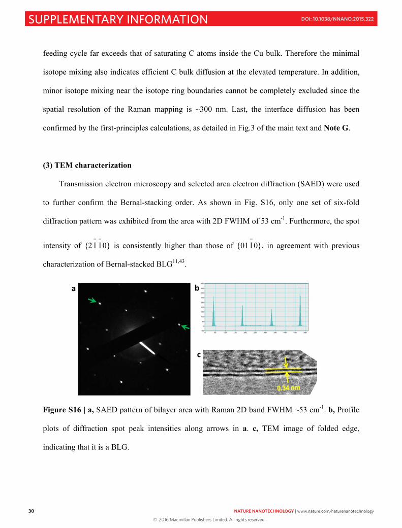
30 NATURE NANOTECHNOLOGY | www.nature.com/naturenanotechnology
SUPPLEMENTARY INFORMATION DOI: 10.1038/NNANO.2015.322
30
feeding cycle far exceeds that of saturating C atoms inside the Cu bulk. Therefore the minimal
isotope mixing also indicates efficient C bulk diffusion at the elevated temperature. In addition,
minor isotope mixing near the isotope ring boundaries cannot be completely excluded since the
spatial resolution of the Raman mapping is ~300 nm. Last, the interface diffusion has been
confirmed by the first-principles calculations, as detailed in Fig.3 of the main text and Note G.
(3) TEM characterization
Transmission electron microscopy and selected area electron diffraction (SAED) were used
to further confirm the Bernal-stacking order. As shown in Fig. S16, only one set of six-fold
diffraction pattern was exhibited from the area with 2D FWHM of 53 cm-1. Furthermore, the spot
intensity of {2−1
−10} is consistently higher than those of {01
−10}, in agreement with previous
characterization of Bernal-stacked BLG11,43.
Figure S16 | a, SAED pattern of bilayer area with Raman 2D band FWHM ~53 cm-1. b, Profile
plots of diffraction spot peak intensities along arrows in a. c, TEM image of folded edge,
indicating that it is a BLG.
31
F. Estimation of C solubility and diffusivity in Cu bulk.
(1) C solubility
It is well known that the C solubility in Cu is extremely low, but our experimental
observations have convinced that appreciable amounts of C can diffuse through the bulk for the
2nd layer growth on the exterior surface of a pocket. In this way, it would be more informative if
there is knowledge of C solubility in Cu at the growth temperature. However, C solubility is lack
of consistent value in literature. In one of the most recent works, Lopez and Mittemeijer25
measured the C solubility in Cu: 7.4 ± 0.5 at. ppm at 1020°C.
One attempt to estimate the C solubility based on our own data is from the amount of 2nd
layer domains grown underneath a full-coverage SLG during the cooling down stage, which are
from the segregation of the dissolved C in the Cu bulk (presumably saturated before the surfaces
being fully passivated by SLG). Obviously we cannot use our Cu pockets for such estimates,
since even though the Cu bulk is saturated with C, C atoms can continuously diffuse through Cu
bulk to the exterior surface as long as the interior surface is not passivated with graphene.
However, in our previous work38 and the result of the control experiment in Fig. S5 of this work,
we observed that there are always ~5% areas of BLG on SLG-covered Cu foil surface. These
BLG domains should be formed by the segregated C from the saturated Cu foil. By using this
data we may estimate the C solubility through the calculations as follows:
Given the standard atomic weight of Cu (63.546 g/mol) and the Cu density (8.96 g/cm3), we
obtain that in a Cu foil of 25 μm thick and 1cm2 area, the number of Cu atoms is NCu = 2.15 ×
1020. The C sp2 bond distance is 0.142 nm, and there are two C atoms in one graphene unit cell.
So, in the area of 1 cm2, there are 3.8 × 10¹⁵ C atoms in graphene if assuming full coverage.
Considering the top and bottom surfaces of a Cu foil of 1cm2 area and 5% coverage, we can get
© 2016 Macmillan Publishers Limited. All rights reserved.
NATURE NANOTECHNOLOGY | www.nature.com/naturenanotechnology 31
SUPPLEMENTARY INFORMATIONDOI: 10.1038/NNANO.2015.322
30
feeding cycle far exceeds that of saturating C atoms inside the Cu bulk. Therefore the minimal
isotope mixing also indicates efficient C bulk diffusion at the elevated temperature. In addition,
minor isotope mixing near the isotope ring boundaries cannot be completely excluded since the
spatial resolution of the Raman mapping is ~300 nm. Last, the interface diffusion has been
confirmed by the first-principles calculations, as detailed in Fig.3 of the main text and Note G.
(3) TEM characterization
Transmission electron microscopy and selected area electron diffraction (SAED) were used
to further confirm the Bernal-stacking order. As shown in Fig. S16, only one set of six-fold
diffraction pattern was exhibited from the area with 2D FWHM of 53 cm-1. Furthermore, the spot
intensity of {2−1
−10} is consistently higher than those of {01
−10}, in agreement with previous
characterization of Bernal-stacked BLG11,43.
Figure S16 | a, SAED pattern of bilayer area with Raman 2D band FWHM ~53 cm-1. b, Profile
plots of diffraction spot peak intensities along arrows in a. c, TEM image of folded edge,
indicating that it is a BLG.
31
F. Estimation of C solubility and diffusivity in Cu bulk.
(1) C solubility
It is well known that the C solubility in Cu is extremely low, but our experimental
observations have convinced that appreciable amounts of C can diffuse through the bulk for the
2nd layer growth on the exterior surface of a pocket. In this way, it would be more informative if
there is knowledge of C solubility in Cu at the growth temperature. However, C solubility is lack
of consistent value in literature. In one of the most recent works, Lopez and Mittemeijer25
measured the C solubility in Cu: 7.4 ± 0.5 at. ppm at 1020°C.
One attempt to estimate the C solubility based on our own data is from the amount of 2nd
layer domains grown underneath a full-coverage SLG during the cooling down stage, which are
from the segregation of the dissolved C in the Cu bulk (presumably saturated before the surfaces
being fully passivated by SLG). Obviously we cannot use our Cu pockets for such estimates,
since even though the Cu bulk is saturated with C, C atoms can continuously diffuse through Cu
bulk to the exterior surface as long as the interior surface is not passivated with graphene.
However, in our previous work38 and the result of the control experiment in Fig. S5 of this work,
we observed that there are always ~5% areas of BLG on SLG-covered Cu foil surface. These
BLG domains should be formed by the segregated C from the saturated Cu foil. By using this
data we may estimate the C solubility through the calculations as follows:
Given the standard atomic weight of Cu (63.546 g/mol) and the Cu density (8.96 g/cm3), we
obtain that in a Cu foil of 25 μm thick and 1cm2 area, the number of Cu atoms is NCu = 2.15 ×
1020. The C sp2 bond distance is 0.142 nm, and there are two C atoms in one graphene unit cell.
So, in the area of 1 cm2, there are 3.8 × 10¹⁵ C atoms in graphene if assuming full coverage.
Considering the top and bottom surfaces of a Cu foil of 1cm2 area and 5% coverage, we can get
© 2016 Macmillan Publishers Limited. All rights reserved.
32 NATURE NANOTECHNOLOGY | www.nature.com/naturenanotechnology
SUPPLEMENTARY INFORMATION DOI: 10.1038/NNANO.2015.322
32
that the number of C atoms in the 2nd layer graphene on the Cu foil surface is NC = 3.8 × 10¹⁴.
The solubility of C in Cu is therefore NC / NCu = 1.8 at. ppm. This value is in the same order of
magnitude as the value measured by Lopez and Mittemeijer25.
We nevertheless note that our number may be an underestimate since the Cu foil is not
necessarily saturated with C during the growth, nor is it necessary that all C segregated from the
bulk Cu to form the 2nd layer graphene upon cooling. It is also safe to say, by following this
estimation procedure, that the C dissolved in the bulk of our Cu pocket cannot lead to the
significant growth of BLG that we observed.
(2) C diffusivity
The diffusivity for solid state diffusion is described by the Arrhenius formula:
kTeDDΔ
−= 0 ,
where Δ is the microscopic kinetic energy barrier for a C atom to hop between adjacent lowest
energy sites in bulk Cu. 0D is given by
ν6
2
0
aD = ,
where a is the length of a hopping step and is equal to the Cu nearest neighbor distance 2.5 Å,
6
2a is from the assumption of 3D random walk, and ν is the attempt frequency, which is
basically the atomic vibration frequency ~ 1013 Hz. With these numbers the C diffusivity is
kTeDΔ
−−= 310 cm2s-1.
33
When T=1300 K, Δ=1 eV (DFT calculation result in this work, Fig. 3d), the diffusivity of C in
bulk Cu is found to be about 1.3×10⁻⁷ cm2s-1. This value is comparable with the C diffusivity in
γ-Fe (fcc Fe), ~5 ×10⁻⁷ cm2s-1 at ~1100 °C (Ref. 44), indicating that C can efficiently diffuse
inside Cu bulk. It is remarkable that although the C solubility of Fe is orders of magnitude larger
than that of Cu, the diffusivity values of C in these two materials are comparable. This again
points out that the diffusivity as a kinetic property is not necessarily strongly correlated with the
solubility, which is a thermal equilibrium property.
G. 2nd Layer Growth Mechanism studied by First-Principles Calculations
Besides the O-activated hydrocarbon dissociation on Cu, large 2nd layer growth requires fast
kinetics for (i) C diffusion in Cu bulk; (ii) C diffusion near the Cu-graphene interface. Overall,
the Cu(111) surfaces with and without graphene top layer are adopted as an example to do the
calculations.
Since the Cu lattice cannot accommodate large C clusters [C-C dimer, CHx (x=1-4), etc.];
At the Cu-graphene interface, these species are also found energetically unfavorable28,45.
Therefore, in this work, only individual C atoms are calculated in various processes.
We perform density functional theory (DFT) calculations using Projector Augmented
Wave (PAW) pseudopotentials 46,47 and the VDW-DF functional,48 as implemented in VASP.49,50
The energy cutoff for the plane wave functions is 400 eV. All structures are relaxed until the
force on each atom is < 0.01 eV/Å. The Cu-graphene interface is modeled by a 4×4 Cu(111)
surface cell with 4 layers, as shown in Fig. S17a. The bottom layer is fixed in the direction
perpendicular to the surface. 5×5×1 Monkhorst-Pack (MP) k-points51 are used (5×5 points in the
surface plane and 1 along the surface normal direction) to sample the Brillouin zone. C atom in
© 2016 Macmillan Publishers Limited. All rights reserved.
NATURE NANOTECHNOLOGY | www.nature.com/naturenanotechnology 33
SUPPLEMENTARY INFORMATIONDOI: 10.1038/NNANO.2015.322
32
that the number of C atoms in the 2nd layer graphene on the Cu foil surface is NC = 3.8 × 10¹⁴.
The solubility of C in Cu is therefore NC / NCu = 1.8 at. ppm. This value is in the same order of
magnitude as the value measured by Lopez and Mittemeijer25.
We nevertheless note that our number may be an underestimate since the Cu foil is not
necessarily saturated with C during the growth, nor is it necessary that all C segregated from the
bulk Cu to form the 2nd layer graphene upon cooling. It is also safe to say, by following this
estimation procedure, that the C dissolved in the bulk of our Cu pocket cannot lead to the
significant growth of BLG that we observed.
(2) C diffusivity
The diffusivity for solid state diffusion is described by the Arrhenius formula:
kTeDDΔ
−= 0 ,
where Δ is the microscopic kinetic energy barrier for a C atom to hop between adjacent lowest
energy sites in bulk Cu. 0D is given by
ν6
2
0
aD = ,
where a is the length of a hopping step and is equal to the Cu nearest neighbor distance 2.5 Å,
6
2a is from the assumption of 3D random walk, and ν is the attempt frequency, which is
basically the atomic vibration frequency ~ 1013 Hz. With these numbers the C diffusivity is
kTeDΔ
−−= 310 cm2s-1.
33
When T=1300 K, Δ=1 eV (DFT calculation result in this work, Fig. 3d), the diffusivity of C in
bulk Cu is found to be about 1.3×10⁻⁷ cm2s-1. This value is comparable with the C diffusivity in
γ-Fe (fcc Fe), ~5 ×10⁻⁷ cm2s-1 at ~1100 °C (Ref. 44), indicating that C can efficiently diffuse
inside Cu bulk. It is remarkable that although the C solubility of Fe is orders of magnitude larger
than that of Cu, the diffusivity values of C in these two materials are comparable. This again
points out that the diffusivity as a kinetic property is not necessarily strongly correlated with the
solubility, which is a thermal equilibrium property.
G. 2nd Layer Growth Mechanism studied by First-Principles Calculations
Besides the O-activated hydrocarbon dissociation on Cu, large 2nd layer growth requires fast
kinetics for (i) C diffusion in Cu bulk; (ii) C diffusion near the Cu-graphene interface. Overall,
the Cu(111) surfaces with and without graphene top layer are adopted as an example to do the
calculations.
Since the Cu lattice cannot accommodate large C clusters [C-C dimer, CHx (x=1-4), etc.];
At the Cu-graphene interface, these species are also found energetically unfavorable28,45.
Therefore, in this work, only individual C atoms are calculated in various processes.
We perform density functional theory (DFT) calculations using Projector Augmented
Wave (PAW) pseudopotentials 46,47 and the VDW-DF functional,48 as implemented in VASP.49,50
The energy cutoff for the plane wave functions is 400 eV. All structures are relaxed until the
force on each atom is < 0.01 eV/Å. The Cu-graphene interface is modeled by a 4×4 Cu(111)
surface cell with 4 layers, as shown in Fig. S17a. The bottom layer is fixed in the direction
perpendicular to the surface. 5×5×1 Monkhorst-Pack (MP) k-points51 are used (5×5 points in the
surface plane and 1 along the surface normal direction) to sample the Brillouin zone. C atom in
© 2016 Macmillan Publishers Limited. All rights reserved.
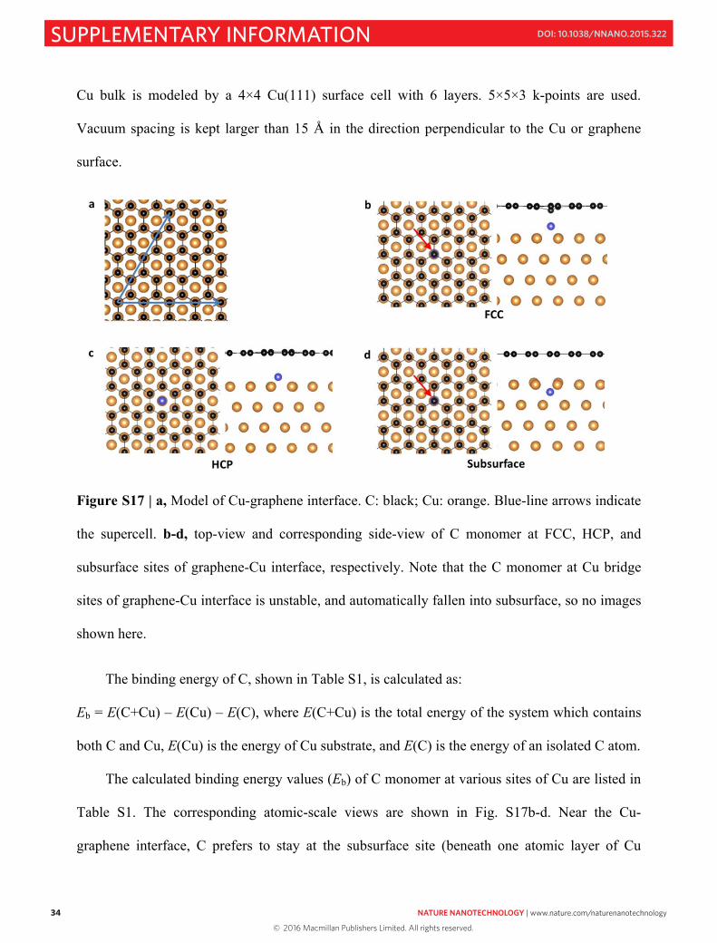
34 NATURE NANOTECHNOLOGY | www.nature.com/naturenanotechnology
SUPPLEMENTARY INFORMATION DOI: 10.1038/NNANO.2015.322
34
Cu bulk is modeled by a 4×4 Cu(111) surface cell with 6 layers. 5×5×3 k-points are used.
Vacuum spacing is kept larger than 15 Å in the direction perpendicular to the Cu or graphene
surface.
Figure S17 | a, Model of Cu-graphene interface. C: black; Cu: orange. Blue-line arrows indicate
the supercell. b-d, top-view and corresponding side-view of C monomer at FCC, HCP, and
subsurface sites of graphene-Cu interface, respectively. Note that the C monomer at Cu bridge
sites of graphene-Cu interface is unstable, and automatically fallen into subsurface, so no images
shown here.
The binding energy of C, shown in Table S1, is calculated as:
Eb = E(C+Cu) – E(Cu) – E(C), where E(C+Cu) is the total energy of the system which contains
both C and Cu, E(Cu) is the energy of Cu substrate, and E(C) is the energy of an isolated C atom.
The calculated binding energy values (Eb) of C monomer at various sites of Cu are listed in
Table S1. The corresponding atomic-scale views are shown in Fig. S17b-d. Near the Cu-
graphene interface, C prefers to stay at the subsurface site (beneath one atomic layer of Cu
35
surface). This is consistent with previous reports28,45,52 and indicates that after bulk diffusion,
most C atoms should sit on the Cu subsurface.
The energy of CHx for the without-O case, shown in Fig. 3, is calculated as: E = E(CHx+Cu)
– E(CH4+Cu) + x[E(Cu+H)-E(Cu)]; and for the with-O case: E = E(CHx+Cu) – E(CH4+Cu) +
x[E(Cu+OH)-E(Cu+O)].
Table S1 | The calculated energetics and diffusion barriers of C atoms during various processes.
The unit is eV/atom.
Since Cu surface is not atomically smooth in real experiments, it is necessary to consider
whether the surface defects would take effects on the dehydrogenation processes. Step edges
have been found to be the most popular defects on Cu surface at elevated temperature. We
calculated the dehydrogenation barriers from CH4 to C monomers. The Cu step is modeled by
cutting the Cu (111) surface along the <011> direction, with a spacing of 3*a*sqrt(3)/2 between
the step edges (where a is the lattice parameter of Cu). The results are shown in Fig. S18a and
compared with the results shown in Fig. 3c. We can clearly see that the step edge can only
© 2016 Macmillan Publishers Limited. All rights reserved.
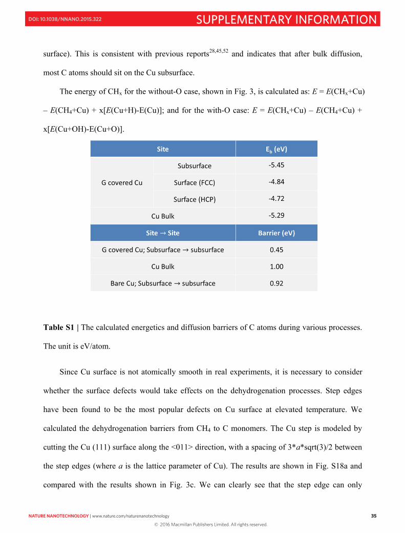
NATURE NANOTECHNOLOGY | www.nature.com/naturenanotechnology 35
SUPPLEMENTARY INFORMATIONDOI: 10.1038/NNANO.2015.322
34
Cu bulk is modeled by a 4×4 Cu(111) surface cell with 6 layers. 5×5×3 k-points are used.
Vacuum spacing is kept larger than 15 Å in the direction perpendicular to the Cu or graphene
surface.
Figure S17 | a, Model of Cu-graphene interface. C: black; Cu: orange. Blue-line arrows indicate
the supercell. b-d, top-view and corresponding side-view of C monomer at FCC, HCP, and
subsurface sites of graphene-Cu interface, respectively. Note that the C monomer at Cu bridge
sites of graphene-Cu interface is unstable, and automatically fallen into subsurface, so no images
shown here.
The binding energy of C, shown in Table S1, is calculated as:
Eb = E(C+Cu) – E(Cu) – E(C), where E(C+Cu) is the total energy of the system which contains
both C and Cu, E(Cu) is the energy of Cu substrate, and E(C) is the energy of an isolated C atom.
The calculated binding energy values (Eb) of C monomer at various sites of Cu are listed in
Table S1. The corresponding atomic-scale views are shown in Fig. S17b-d. Near the Cu-
graphene interface, C prefers to stay at the subsurface site (beneath one atomic layer of Cu
35
surface). This is consistent with previous reports28,45,52 and indicates that after bulk diffusion,
most C atoms should sit on the Cu subsurface.
The energy of CHx for the without-O case, shown in Fig. 3, is calculated as: E = E(CHx+Cu)
– E(CH4+Cu) + x[E(Cu+H)-E(Cu)]; and for the with-O case: E = E(CHx+Cu) – E(CH4+Cu) +
x[E(Cu+OH)-E(Cu+O)].
Table S1 | The calculated energetics and diffusion barriers of C atoms during various processes.
The unit is eV/atom.
Since Cu surface is not atomically smooth in real experiments, it is necessary to consider
whether the surface defects would take effects on the dehydrogenation processes. Step edges
have been found to be the most popular defects on Cu surface at elevated temperature. We
calculated the dehydrogenation barriers from CH4 to C monomers. The Cu step is modeled by
cutting the Cu (111) surface along the <011> direction, with a spacing of 3*a*sqrt(3)/2 between
the step edges (where a is the lattice parameter of Cu). The results are shown in Fig. S18a and
compared with the results shown in Fig. 3c. We can clearly see that the step edge can only
© 2016 Macmillan Publishers Limited. All rights reserved.
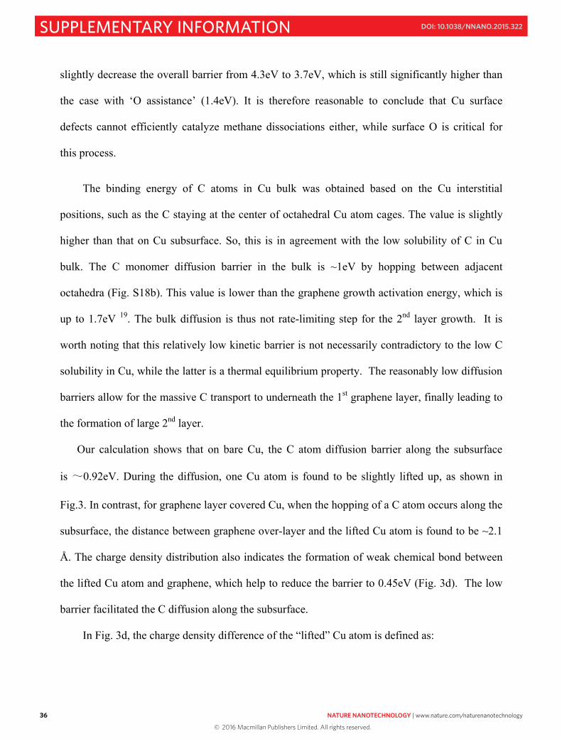
36 NATURE NANOTECHNOLOGY | www.nature.com/naturenanotechnology
SUPPLEMENTARY INFORMATION DOI: 10.1038/NNANO.2015.322
36
slightly decrease the overall barrier from 4.3eV to 3.7eV, which is still significantly higher than
the case with ‘O assistance’ (1.4eV). It is therefore reasonable to conclude that Cu surface
defects cannot efficiently catalyze methane dissociations either, while surface O is critical for
this process.
The binding energy of C atoms in Cu bulk was obtained based on the Cu interstitial
positions, such as the C staying at the center of octahedral Cu atom cages. The value is slightly
higher than that on Cu subsurface. So, this is in agreement with the low solubility of C in Cu
bulk. The C monomer diffusion barrier in the bulk is ~1eV by hopping between adjacent
octahedra (Fig. S18b). This value is lower than the graphene growth activation energy, which is
up to 1.7eV 19. The bulk diffusion is thus not rate-limiting step for the 2nd layer growth. It is
worth noting that this relatively low kinetic barrier is not necessarily contradictory to the low C
solubility in Cu, while the latter is a thermal equilibrium property. The reasonably low diffusion
barriers allow for the massive C transport to underneath the 1st graphene layer, finally leading to
the formation of large 2nd layer.
Our calculation shows that on bare Cu, the C atom diffusion barrier along the subsurface
is ~0.92eV. During the diffusion, one Cu atom is found to be slightly lifted up, as shown in
Fig.3. In contrast, for graphene layer covered Cu, when the hopping of a C atom occurs along the
subsurface, the distance between graphene over-layer and the lifted Cu atom is found to be ~2.1
Å. The charge density distribution also indicates the formation of weak chemical bond between
the lifted Cu atom and graphene, which help to reduce the barrier to 0.45eV (Fig. 3d). The low
barrier facilitated the C diffusion along the subsurface.
In Fig. 3d, the charge density difference of the “lifted” Cu atom is defined as:
37
ρ(Cu+substrate+graphene) - ρ(substrate+graphene) - ρ(Cu atom), where the first term is
the total charge density of the whole system, the second term is the charge density of the system
without the “lifted” Cu atom (other atoms are in fixed positions), and the last term is the charge
density of the isolated Cu atom.”
From the calculations, we established that at atomic-scale the C diffusion through Cu bulk
and interface diffusion along the Cu subsurface are reasonable and can be incorporated into the
graphene growth steps for the large 2nd graphene layer.
Figure S18 | a, Cu (111) step edge dehydrogenation processes and the associated barriers. Inset
shows the equilibrium positions of each CHx radical at Cu step edges. The red and black lines are
for the ideal Cu and for the OR-Cu, respectively, as shown in Fig. 3c of the main text. b, C atom
diffusion inside the Cu bulk. The three panels show the initial, transition, and final states of the
hopping process. The Cu octahedron is found to be slightly distorted at the transition state.
H. Device fabrication and transport measurements
The fabrication process of the BLG devices was schematically shown in Fig. S19. First, the
BLG domains were transferred onto h-BN/SiO2/Si substrates (Step 1) by the PMMA-assisted
method. Then, electron-beam lithography (EBL), reactive ion etching, and physical vapor
© 2016 Macmillan Publishers Limited. All rights reserved.
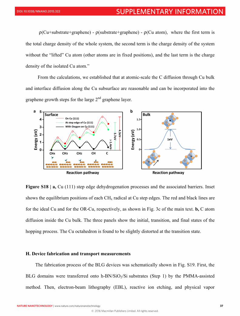
NATURE NANOTECHNOLOGY | www.nature.com/naturenanotechnology 37
SUPPLEMENTARY INFORMATIONDOI: 10.1038/NNANO.2015.322
36
slightly decrease the overall barrier from 4.3eV to 3.7eV, which is still significantly higher than
the case with ‘O assistance’ (1.4eV). It is therefore reasonable to conclude that Cu surface
defects cannot efficiently catalyze methane dissociations either, while surface O is critical for
this process.
The binding energy of C atoms in Cu bulk was obtained based on the Cu interstitial
positions, such as the C staying at the center of octahedral Cu atom cages. The value is slightly
higher than that on Cu subsurface. So, this is in agreement with the low solubility of C in Cu
bulk. The C monomer diffusion barrier in the bulk is ~1eV by hopping between adjacent
octahedra (Fig. S18b). This value is lower than the graphene growth activation energy, which is
up to 1.7eV 19. The bulk diffusion is thus not rate-limiting step for the 2nd layer growth. It is
worth noting that this relatively low kinetic barrier is not necessarily contradictory to the low C
solubility in Cu, while the latter is a thermal equilibrium property. The reasonably low diffusion
barriers allow for the massive C transport to underneath the 1st graphene layer, finally leading to
the formation of large 2nd layer.
Our calculation shows that on bare Cu, the C atom diffusion barrier along the subsurface
is ~0.92eV. During the diffusion, one Cu atom is found to be slightly lifted up, as shown in
Fig.3. In contrast, for graphene layer covered Cu, when the hopping of a C atom occurs along the
subsurface, the distance between graphene over-layer and the lifted Cu atom is found to be ~2.1
Å. The charge density distribution also indicates the formation of weak chemical bond between
the lifted Cu atom and graphene, which help to reduce the barrier to 0.45eV (Fig. 3d). The low
barrier facilitated the C diffusion along the subsurface.
In Fig. 3d, the charge density difference of the “lifted” Cu atom is defined as:
37
ρ(Cu+substrate+graphene) - ρ(substrate+graphene) - ρ(Cu atom), where the first term is
the total charge density of the whole system, the second term is the charge density of the system
without the “lifted” Cu atom (other atoms are in fixed positions), and the last term is the charge
density of the isolated Cu atom.”
From the calculations, we established that at atomic-scale the C diffusion through Cu bulk
and interface diffusion along the Cu subsurface are reasonable and can be incorporated into the
graphene growth steps for the large 2nd graphene layer.
Figure S18 | a, Cu (111) step edge dehydrogenation processes and the associated barriers. Inset
shows the equilibrium positions of each CHx radical at Cu step edges. The red and black lines are
for the ideal Cu and for the OR-Cu, respectively, as shown in Fig. 3c of the main text. b, C atom
diffusion inside the Cu bulk. The three panels show the initial, transition, and final states of the
hopping process. The Cu octahedron is found to be slightly distorted at the transition state.
H. Device fabrication and transport measurements
The fabrication process of the BLG devices was schematically shown in Fig. S19. First, the
BLG domains were transferred onto h-BN/SiO2/Si substrates (Step 1) by the PMMA-assisted
method. Then, electron-beam lithography (EBL), reactive ion etching, and physical vapor
© 2016 Macmillan Publishers Limited. All rights reserved.
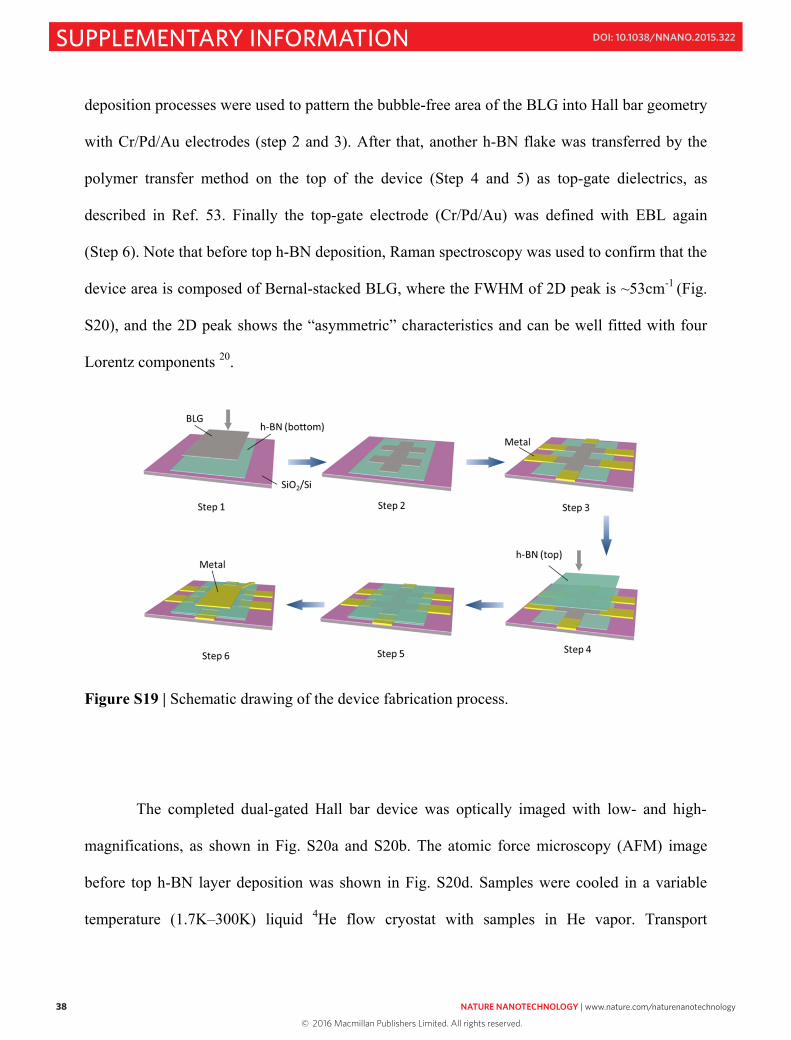
38 NATURE NANOTECHNOLOGY | www.nature.com/naturenanotechnology
SUPPLEMENTARY INFORMATION DOI: 10.1038/NNANO.2015.322
38
deposition processes were used to pattern the bubble-free area of the BLG into Hall bar geometry
with Cr/Pd/Au electrodes (step 2 and 3). After that, another h-BN flake was transferred by the
polymer transfer method on the top of the device (Step 4 and 5) as top-gate dielectrics, as
described in Ref. 53. Finally the top-gate electrode (Cr/Pd/Au) was defined with EBL again
(Step 6). Note that before top h-BN deposition, Raman spectroscopy was used to confirm that the
device area is composed of Bernal-stacked BLG, where the FWHM of 2D peak is ~53cm-1 (Fig.
S20), and the 2D peak shows the “asymmetric” characteristics and can be well fitted with four
Lorentz components 20.
Figure S19 | Schematic drawing of the device fabrication process.
The completed dual-gated Hall bar device was optically imaged with low- and high-
magnifications, as shown in Fig. S20a and S20b. The atomic force microscopy (AFM) image
before top h-BN layer deposition was shown in Fig. S20d. Samples were cooled in a variable
temperature (1.7K–300K) liquid 4He flow cryostat with samples in He vapor. Transport
39
measurements were acquired in a four-terminal geometry using a standard lock-in technique at
17Hz.
Figure S20 | a, b, The low- and high-magnification optical images of two devices encapsulated
between two h-BN flakes. c, The schematic picture of the device cross section. d, AFM image of
the device before top-gate dielectric deposition, as circled by the green dash-line in c. e, The
Raman spectrum of the device area of the BLG. f, The Lorentz fitting of 2D band of the Bernal-
stacked BLG. On h-BN, we can clearly see the “asymmetry” of the 2D band.
From the electrical transport measurement (Fig. S21), the extracted mobility is ~20,000
cm2V-1S-1 at room temperature. At liquid He temperature, we can clearly observe the quantum
Hall states at a magnetic field of 6 T with filling factors ν=±4, ±8, and ±12, in agreement with
© 2016 Macmillan Publishers Limited. All rights reserved.
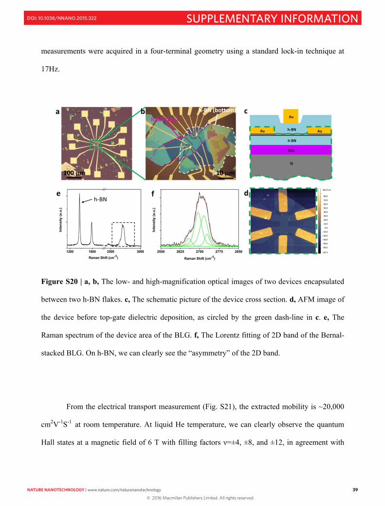
NATURE NANOTECHNOLOGY | www.nature.com/naturenanotechnology 39
SUPPLEMENTARY INFORMATIONDOI: 10.1038/NNANO.2015.322
38
deposition processes were used to pattern the bubble-free area of the BLG into Hall bar geometry
with Cr/Pd/Au electrodes (step 2 and 3). After that, another h-BN flake was transferred by the
polymer transfer method on the top of the device (Step 4 and 5) as top-gate dielectrics, as
described in Ref. 53. Finally the top-gate electrode (Cr/Pd/Au) was defined with EBL again
(Step 6). Note that before top h-BN deposition, Raman spectroscopy was used to confirm that the
device area is composed of Bernal-stacked BLG, where the FWHM of 2D peak is ~53cm-1 (Fig.
S20), and the 2D peak shows the “asymmetric” characteristics and can be well fitted with four
Lorentz components 20.
Figure S19 | Schematic drawing of the device fabrication process.
The completed dual-gated Hall bar device was optically imaged with low- and high-
magnifications, as shown in Fig. S20a and S20b. The atomic force microscopy (AFM) image
before top h-BN layer deposition was shown in Fig. S20d. Samples were cooled in a variable
temperature (1.7K–300K) liquid 4He flow cryostat with samples in He vapor. Transport
39
measurements were acquired in a four-terminal geometry using a standard lock-in technique at
17Hz.
Figure S20 | a, b, The low- and high-magnification optical images of two devices encapsulated
between two h-BN flakes. c, The schematic picture of the device cross section. d, AFM image of
the device before top-gate dielectric deposition, as circled by the green dash-line in c. e, The
Raman spectrum of the device area of the BLG. f, The Lorentz fitting of 2D band of the Bernal-
stacked BLG. On h-BN, we can clearly see the “asymmetry” of the 2D band.
From the electrical transport measurement (Fig. S21), the extracted mobility is ~20,000
cm2V-1S-1 at room temperature. At liquid He temperature, we can clearly observe the quantum
Hall states at a magnetic field of 6 T with filling factors ν=±4, ±8, and ±12, in agreement with
© 2016 Macmillan Publishers Limited. All rights reserved.
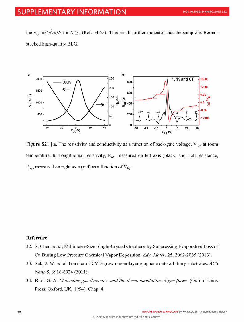
40 NATURE NANOTECHNOLOGY | www.nature.com/naturenanotechnology
SUPPLEMENTARY INFORMATION DOI: 10.1038/NNANO.2015.322
40
the σxy=±(4e2/h)N for N ≥1 (Ref. 54,55). This result further indicates that the sample is Bernal-
stacked high-quality BLG.
Figure S21 | a, The resistivity and conductivity as a function of back-gate voltage, Vbg, at room
temperature. b, Longitudinal resistivity, Rxx, measured on left axis (black) and Hall resistance,
Rxy, measured on right axis (red) as a function of Vbg.
Reference:
32. S. Chen et al., Millimeter-Size Single-Crystal Graphene by Suppressing Evaporative Loss of
Cu During Low Pressure Chemical Vapor Deposition. Adv. Mater. 25, 2062-2065 (2013).
33. Suk, J. W. et al. Transfer of CVD-grown monolayer graphene onto arbitrary substrates. ACS
Nano 5, 6916-6924 (2011).
34. Bird, G. A. Molecular gas dynamics and the direct simulation of gas flows. (Oxford Univ.
Press, Oxford. UK, 1994), Chap. 4.
41
35. Malek, K. & Coppens, M. O. Knudsen self- and Fickian diffusion in rough nanoporous
media. J. Chem. Phys.119, 2801-2811 (2003).
36. Gang, H. & Ye, W. A Macro Model for Squeeze-film Air Damping in the Free-Molecule
Regime. Phys. Fluids 22, 012001 (2010).
37. Naris, S., Valougeorgis, D., Kalempa, D. & Sharipov, F. Gaseous mixture flow between two
parallel plates in the whole range of the gas rarefaction. Physica A: Statistical Mechanics
and its Applications 336, 294-318 (2004).
38. Li, X. et al. Large-area synthesis of high-quality and uniform graphene films on copper foils.
Science 324, 1312-1314 (2009).
39. Su, C. Y. et al. Direct formation of wafer scale graphene thin layers on insulating substrates
by chemical vapor deposition, Nano Lett. 11, 3612-3616 (2011).
40. Nie, S. et al. Growth from below: bilayer graphene on copper by chemical vapor deposition,
New J. Phys. 14, 093028 (2012).
41. Cai, W. et al. Synthesis and solid-state NMR structural characterization of 13C-labeled
graphite oxide. Science 321, 1815-1817 (2008).
42. Li, X. et al. Graphene films with large domain size by a two-step chemical vapor deposition
process. Nano Lett. 10, 4328-4334 (2010).
43. Meyer, J. C. et al. On the roughness of single- and bi-layer graphene membranes. Solid State
Commun. 143, 101-109 (2007).
44. Edited by Brandes E. A. & Brook, G. B. Smithells Metals Reference Book, 7th Edition.
(Butterworth-Heinemann, March 30, 1998).
45. Zhang, X., Wang, L., Xin, J., Yakobson, B. I. & Ding, F. Role of hydrogen in graphene
chemical vapor deposition growth on a copper surface, J. Am. Chem. Soc. 136, 3040-3047
(2014).
46. Kresse, G. & Joubert, D. From ultrasoft pseudopotentials to the projector augmented-wave
method. Phys. Rev. B 59, 1758 (1999).
47. Blöchl, P. E. Projector augmented-wave method. Phys. Rev. B 50, 17953 (1994).
48. Klimeš, J. Bowler, D. R. & Michaelides, A. Van der Waals density functionals applied to
solids. Phys. Rev. B 83, 195131 (2011).
49. Kresse, G. & Hafner, J. Ab initio molecular dynamics for liquid metals. Phys. Rev. B 47, 558
(1993).
© 2016 Macmillan Publishers Limited. All rights reserved.
NATURE NANOTECHNOLOGY | www.nature.com/naturenanotechnology 41
SUPPLEMENTARY INFORMATIONDOI: 10.1038/NNANO.2015.322
40
the σxy=±(4e2/h)N for N ≥1 (Ref. 54,55). This result further indicates that the sample is Bernal-
stacked high-quality BLG.
Figure S21 | a, The resistivity and conductivity as a function of back-gate voltage, Vbg, at room
temperature. b, Longitudinal resistivity, Rxx, measured on left axis (black) and Hall resistance,
Rxy, measured on right axis (red) as a function of Vbg.
Reference:
32. S. Chen et al., Millimeter-Size Single-Crystal Graphene by Suppressing Evaporative Loss of
Cu During Low Pressure Chemical Vapor Deposition. Adv. Mater. 25, 2062-2065 (2013).
33. Suk, J. W. et al. Transfer of CVD-grown monolayer graphene onto arbitrary substrates. ACS
Nano 5, 6916-6924 (2011).
34. Bird, G. A. Molecular gas dynamics and the direct simulation of gas flows. (Oxford Univ.
Press, Oxford. UK, 1994), Chap. 4.
41
35. Malek, K. & Coppens, M. O. Knudsen self- and Fickian diffusion in rough nanoporous
media. J. Chem. Phys.119, 2801-2811 (2003).
36. Gang, H. & Ye, W. A Macro Model for Squeeze-film Air Damping in the Free-Molecule
Regime. Phys. Fluids 22, 012001 (2010).
37. Naris, S., Valougeorgis, D., Kalempa, D. & Sharipov, F. Gaseous mixture flow between two
parallel plates in the whole range of the gas rarefaction. Physica A: Statistical Mechanics
and its Applications 336, 294-318 (2004).
38. Li, X. et al. Large-area synthesis of high-quality and uniform graphene films on copper foils.
Science 324, 1312-1314 (2009).
39. Su, C. Y. et al. Direct formation of wafer scale graphene thin layers on insulating substrates
by chemical vapor deposition, Nano Lett. 11, 3612-3616 (2011).
40. Nie, S. et al. Growth from below: bilayer graphene on copper by chemical vapor deposition,
New J. Phys. 14, 093028 (2012).
41. Cai, W. et al. Synthesis and solid-state NMR structural characterization of 13C-labeled
graphite oxide. Science 321, 1815-1817 (2008).
42. Li, X. et al. Graphene films with large domain size by a two-step chemical vapor deposition
process. Nano Lett. 10, 4328-4334 (2010).
43. Meyer, J. C. et al. On the roughness of single- and bi-layer graphene membranes. Solid State
Commun. 143, 101-109 (2007).
44. Edited by Brandes E. A. & Brook, G. B. Smithells Metals Reference Book, 7th Edition.
(Butterworth-Heinemann, March 30, 1998).
45. Zhang, X., Wang, L., Xin, J., Yakobson, B. I. & Ding, F. Role of hydrogen in graphene
chemical vapor deposition growth on a copper surface, J. Am. Chem. Soc. 136, 3040-3047
(2014).
46. Kresse, G. & Joubert, D. From ultrasoft pseudopotentials to the projector augmented-wave
method. Phys. Rev. B 59, 1758 (1999).
47. Blöchl, P. E. Projector augmented-wave method. Phys. Rev. B 50, 17953 (1994).
48. Klimeš, J. Bowler, D. R. & Michaelides, A. Van der Waals density functionals applied to
solids. Phys. Rev. B 83, 195131 (2011).
49. Kresse, G. & Hafner, J. Ab initio molecular dynamics for liquid metals. Phys. Rev. B 47, 558
(1993).
© 2016 Macmillan Publishers Limited. All rights reserved.
42 NATURE NANOTECHNOLOGY | www.nature.com/naturenanotechnology
SUPPLEMENTARY INFORMATION DOI: 10.1038/NNANO.2015.322
42
50. Kresse, G. & Furthmüller, J. Efficient iterative schemes for ab initio total-energy
calculations using a plane-wave basis set. Phys. Rev. B 54, 11169 (1996).
51. Monkhorst, H. J. & Pack, J. D. Special points for Brillouin-zone integrations. Phys. Rev. B
13, 5188 (1976).
52. Yazyev, O. V. & Pasquarello, A. Effect of metal element in catalytic growth of carbon
nanotubes, Phys. Rev. Lett. 100, 156102 (2008)
53. Dean, C. R. et al. Boron nitride substrates for high-quality graphene electronics. Nat.
Nanotechnol., 5, 722-726 (2010).
54. Novoselov, K. S. et al. Unconventional quantum Hall effect and Berry’s phase of 2π in
bilayer graphene. Nat. Phys. 2, 177-180 (2006).
55. Fallahazad, B. et al. Quantum Hall effect in Bernal stacked and twisted bilayer graphene
grown on Cu by chemical vapor deposition. Phys. Rev. B 85, 201408(2012).
© 2016 Macmillan Publishers Limited. All rights reserved.