Embed Size (px)
Citation preview
CoPEC
1ECEN5807
ECEN 5807
Discrete-Time Modeling and Compensator Design for
Digitally-Controlled
Switched-Mode Power Converters
CoPEC
2ECEN5807
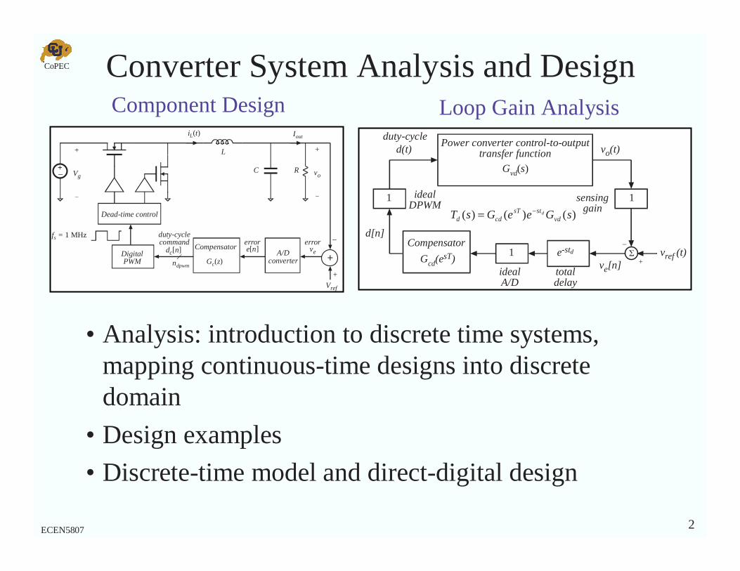
Converter System Analysis and Design
• Analysis: introduction to discrete time systems, mapping continuous-time designs into discrete domain
• Design examples
• Discrete-time model and direct-digital design
Compensatord[n]
Gcd(esT)
Gvd(s)
Power converter control-to-outputtransfer function vo(t)
duty-cycle
idealA/D
ve[n]vref (t)
d(t)
Σ+
_
1idealDPWM
1
e-std1
sensinggain
totaldelay
)()()( sGeeGsT vdstsT
cddd−=
+–
L
iL(t)
+
Vg
_
+
vo
_
Vref
C
Dead-time control
+
_
+DigitalPWM
Compensator
fs = 1 MHz duty-cyclecommand
Iout
R
ve
errordc[n]
Gc(z)ndpwm
e[n]error
A/Dconverter
Component Design Loop Gain Analysis
CoPEC
3ECEN5807
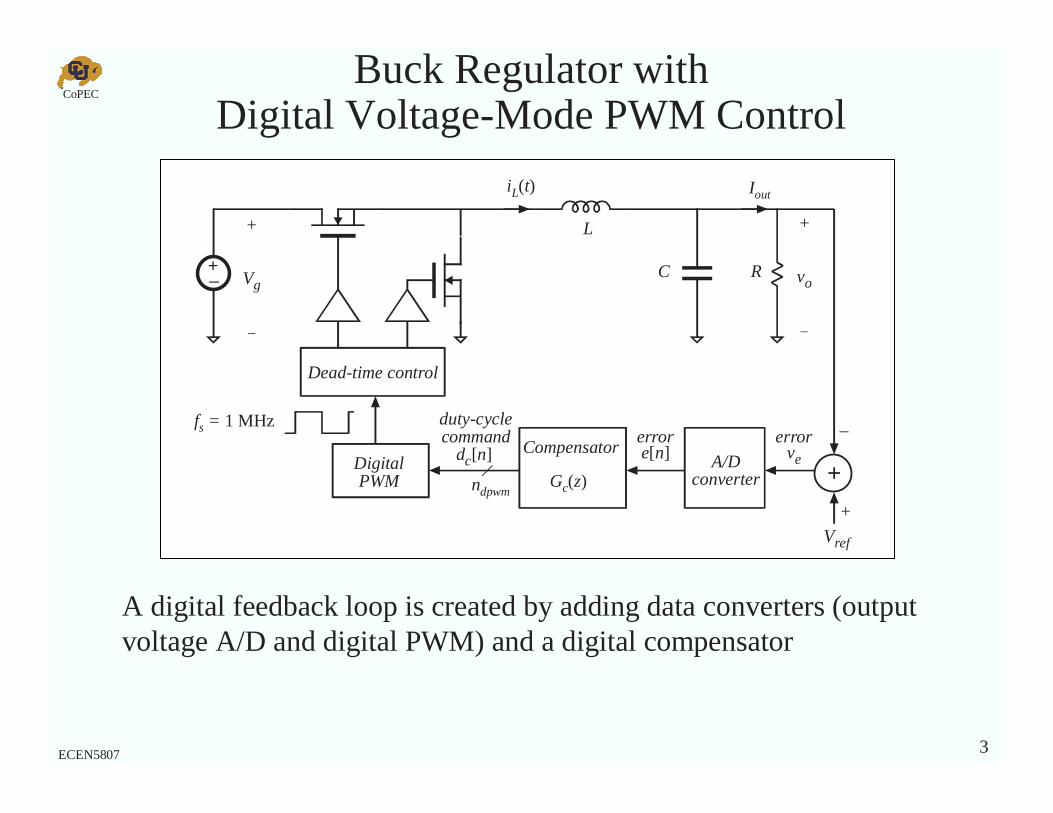
Buck Regulator with Digital Voltage-Mode PWM Control
+–
L
iL(t)
+
Vg
_
+
vo
_
Vref
C
Dead-time control
+
_
+DigitalPWM
Compensator
fs = 1 MHz duty-cyclecommand
Iout
R
ve
errordc[n]
Gc(z)ndpwm
e[n]error
A/Dconverter
A digital feedback loop is created by adding data converters (output voltage A/D and digital PWM) and a digital compensator
CoPEC
4ECEN5807
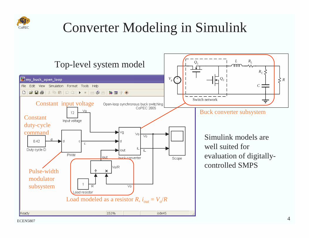
Converter Modeling in Simulink
+–
Vg
Q1L RL
Q2
C
RC
R
Switch network
Load modeled as a resistor R, iout = Vo/R
Pulse-width modulatorsubsystem
Constant duty-cycle command
Constant input voltage
Top-level system model
Buck converter subsystem
Simulink models are well suited for evaluation of digitally-controlled SMPS
CoPEC
5ECEN5807
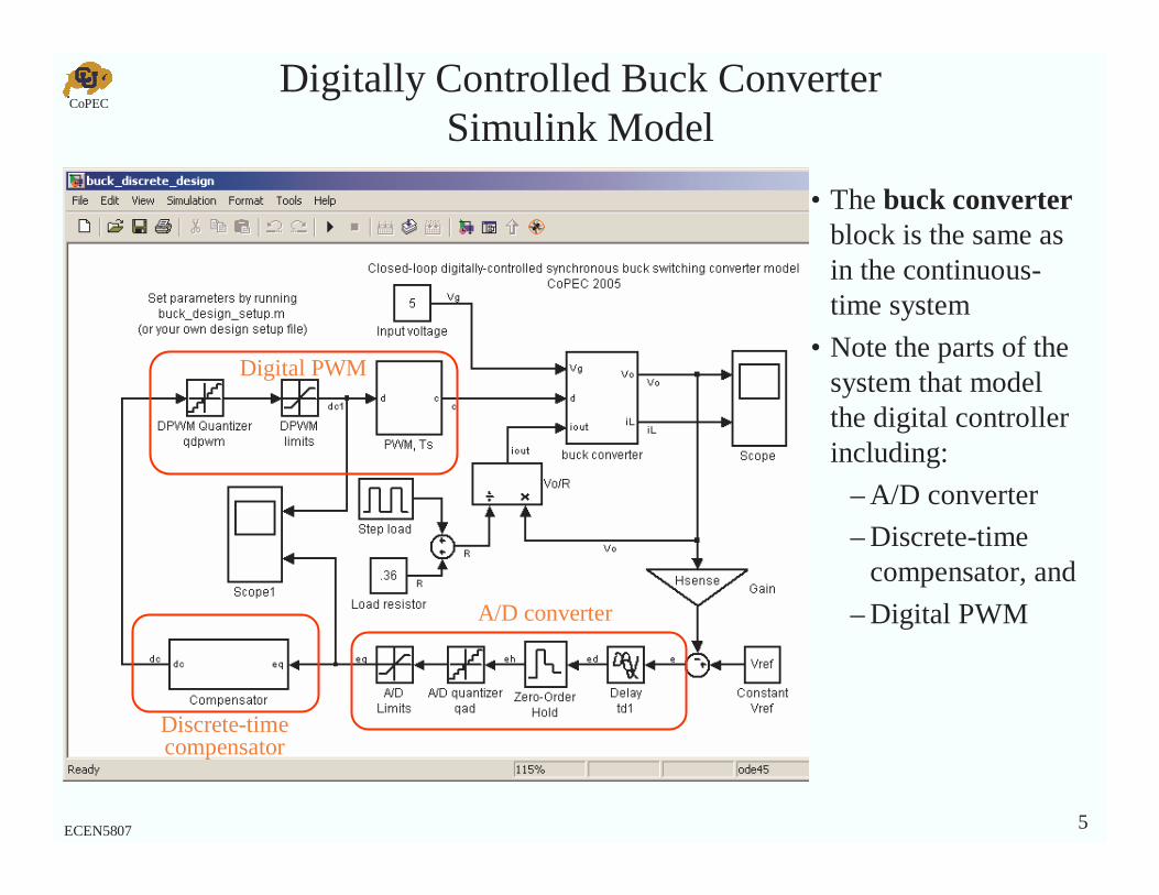
Digitally Controlled Buck ConverterSimulink Model
• The buck converterblock is the same as in the continuous-time system
• Note the parts of the system that model the digital controller including:
– A/D converter
– Discrete-time compensator, and
– Digital PWM
Digital PWM
Discrete-time compensator
A/D converter
CoPEC
6ECEN5807
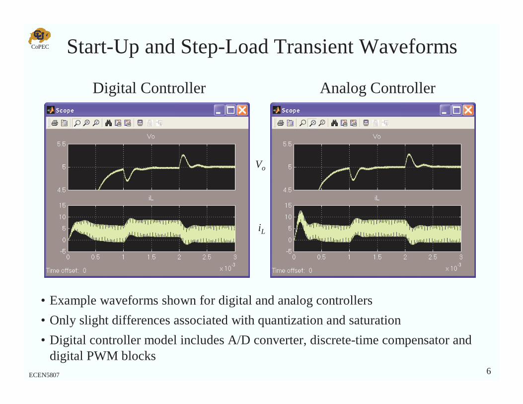
Start-Up and Step-Load Transient Waveforms
Vo
iL
• Example waveforms shown for digital and analog controllers
• Only slight differences associated with quantization and saturation
• Digital controller model includes A/D converter, discrete-time compensator and digital PWM blocks
Digital Controller Analog Controller
CoPEC
7ECEN5807
Discrete-Time System Modeling and Compensator Design
Discrete-time emulation approach
• Re-use known (averaged) models and standard analog compensator design techniques
• Map to discrete time
Direct approach
• Discrete-time converter model
• Direct-digital compensator design
CoPEC
8ECEN5807
Benefits of Analog Design Approach
• Large and small-signal averaged models of all system blocks are readily available and well understood
• Complete design performed in the frequency domain• Design oriented analysis based on intuitive relationships
between frequency response and system specifications• Extensive design experience and existing, proven designs
available
Goal: tap the benefits above & extend to design of digital controllers for switching convertersFirst, compare continuous and discrete designs for a simple integral compensator …
CoPEC
9ECEN5807
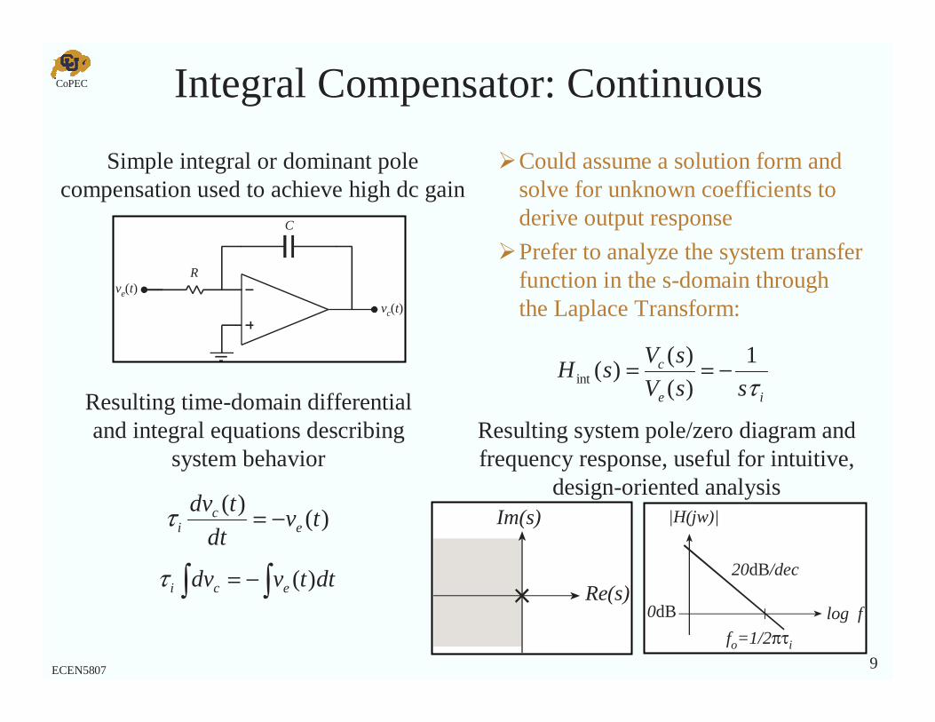
Integral Compensator: Continuous
Simple integral or dominant pole compensation used to achieve high dc gain
)()(
tvdt
tdve
ci −=τ
∫ ∫−= dttvdv eci )(τ
ie
c
ssV
sVsH
τ1
)(
)()(int −==
log f
|H(jw)|
20dB/dec
0dB
fo=1/2πτi
C
Rve(t)
vc(t)
Re(s)
Im(s)
Resulting time-domain differential and integral equations describing
system behavior
Could assume a solution form and solve for unknown coefficients to derive output response
Prefer to analyze the system transfer function in the s-domain through the Laplace Transform:
Resulting system pole/zero diagram and frequency response, useful for intuitive,
design-oriented analysis
CoPEC
10ECEN5807
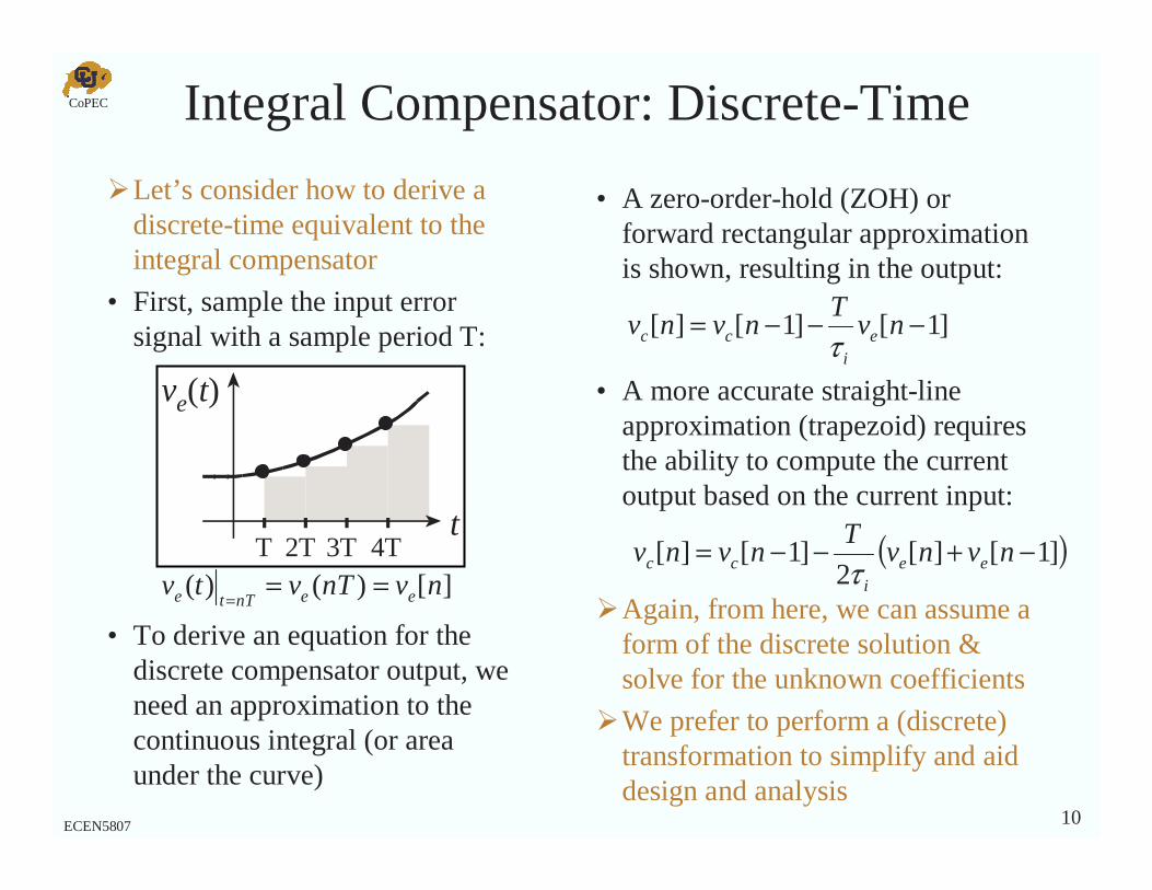
Integral Compensator: Discrete-Time
][)()( nvnTvtv eenTte ===
t
ve(t)
T 2T 3T 4T
Let’s consider how to derive a discrete-time equivalent to the integral compensator
• First, sample the input error signal with a sample period T:
• To derive an equation for the discrete compensator output, we need an approximation to the continuous integral (or area under the curve)
• A zero-order-hold (ZOH) or forward rectangular approximation is shown, resulting in the output:
]1[]1[][ −−−= nvT
nvnv ei
cc τ• A more accurate straight-line
approximation (trapezoid) requires the ability to compute the current output based on the current input:
( )]1[][2
]1[][ −+−−= nvnvT
nvnv eei
cc τAgain, from here, we can assume a form of the discrete solution & solve for the unknown coefficients
We prefer to perform a (discrete) transformation to simplify and aid design and analysis
CoPEC
11ECEN5807
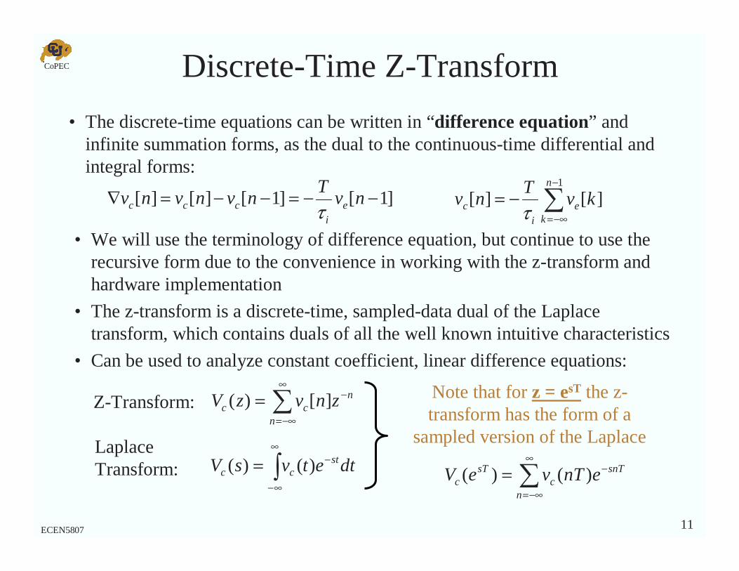
Discrete-Time Z-Transform
• The discrete-time equations can be written in “difference equation” and infinite summation forms, as the dual to the continuous-time differential and integral forms:
]1[]1[][][ −−=−−=∇ nvT
nvnvnv ei
ccc τ ∑−
−∞=
−=1
][][n
ke
ic kv
Tnv
τ• We will use the terminology of difference equation, but continue to use the
recursive form due to the convenience in working with the z-transform and hardware implementation
• The z-transform is a discrete-time, sampled-data dual of the Laplace transform, which contains duals of all the well known intuitive characteristics
• Can be used to analyze constant coefficient, linear difference equations:
∑∞
−∞=
−=n
ncc znvzV ][)(
∫∞
∞−
−= dtetvsV stcc )()(
Z-Transform:
Laplace Transform:
Note that for z = esT the z-transform has the form of a
sampled version of the Laplace
∑∞
−∞=
−=n
snTc
sTc enTveV )()(
CoPEC
12ECEN5807
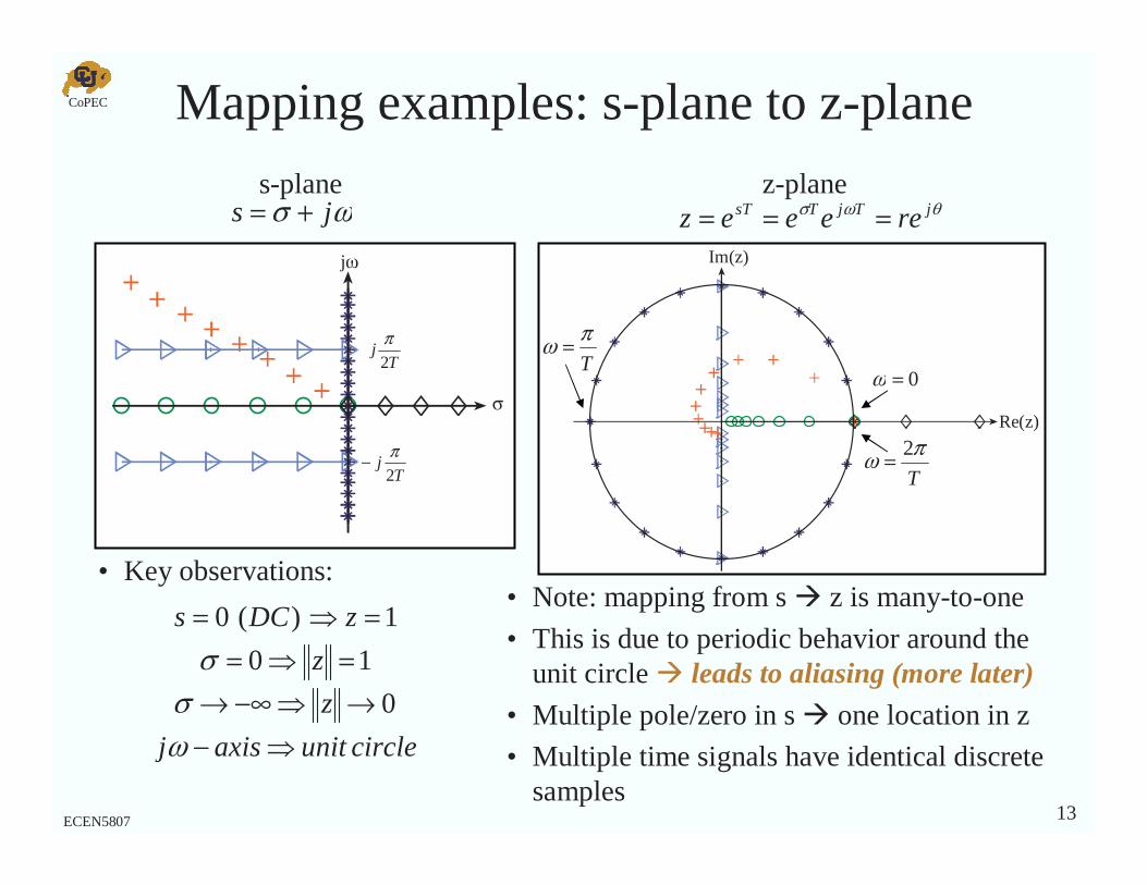
Mapping: s-plane to z-plane
• As noted, with z = esT the z-transform has the form of a sampled version of the Laplace transform
• For complete mapping from the s-domain to z-domain, an approximation to the integral is required
• Note that the s-plane stability boundary, s=jω, maps to the unit circle in the z-plane (z = ejωT) s-plane “left-half-plane (LHP)” will map to considerations “inside the unit-circle” of the z-plane
CoPEC
13ECEN5807
Mapping examples: s-plane to z-plane
σ
jω
Tj
2
π
Tj
2
π−
Im(z)
Re(z)
• Key observations:
0=ωT
πω =
circleunitaxisj
z
z
zDCs
⇒−→⇒−∞→=⇒==⇒=
ωσσ
0
10
1)(0
ωσ js += θωσ jTjTsT reeeez ===s-plane z-plane
• Note: mapping from s z is many-to-one
• This is due to periodic behavior around the unit circle leads to aliasing (more later)
• Multiple pole/zero in s one location in z
• Multiple time signals have identical discrete samples
T
πω 2=
CoPEC
14ECEN5807
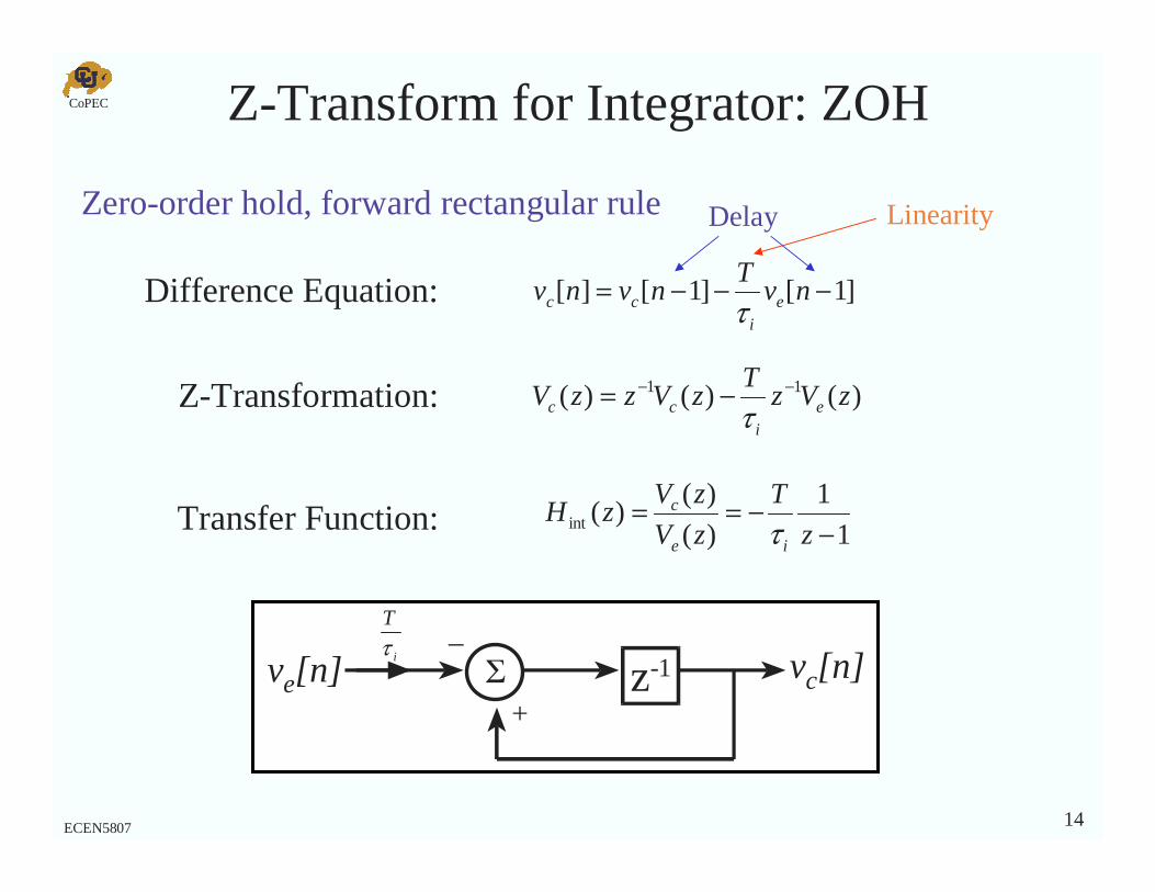
Z-Transform for Integrator: ZOH
]1[]1[][ −−−= nvT
nvnv ei
cc τDifference Equation:
Delay Linearity
Z-Transformation: )()()( 11 zVzT
zVzzV ei
cc−− −=
τ
Transfer Function: 1
1
)(
)()(int −
−==z
T
zV
zVzH
ie
c
τ
Σve[n] vc[n]+
z-1_
i
T
τ
Zero-order hold, forward rectangular rule
CoPEC
15ECEN5807
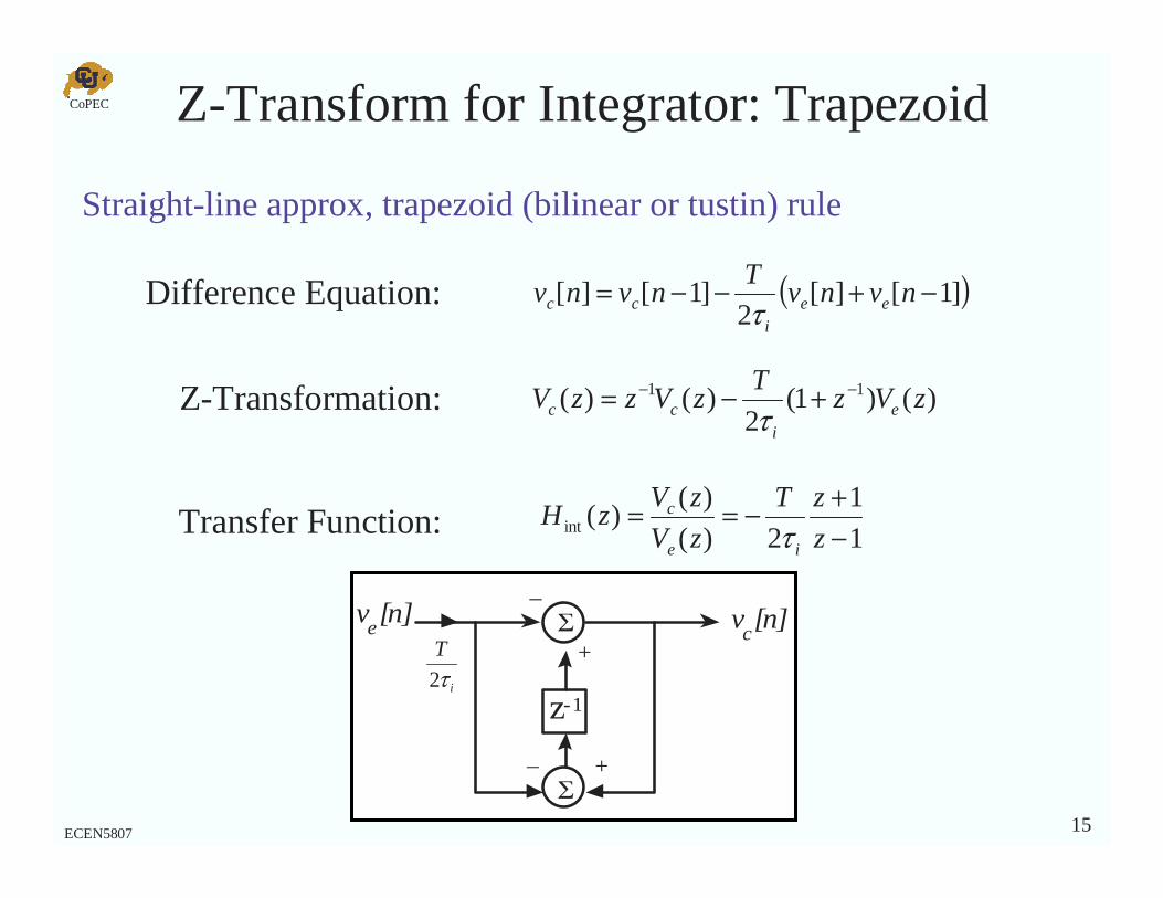
Z-Transform for Integrator: Trapezoid
( )]1[][2
]1[][ −+−−= nvnvT
nvnv eei
cc τ
Straight-line approx, trapezoid (bilinear or tustin) rule
Difference Equation:
Z-Transformation: )()1(2
)()( 11 zVzT
zVzzV ei
cc−− +−=
τ
Transfer Function: 1
1
2)(
)()(int −
+−==z
zT
zV
zVzH
ie
c
τ
Σve[n] v
c[n]
+
z-1
_
Σ+_
i
T
τ2
CoPEC
16ECEN5807
Σve[n] vc[n]+
z-1_
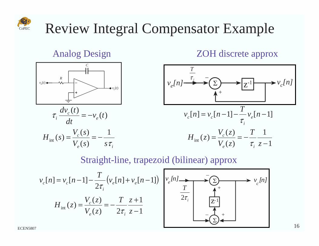
Review Integral Compensator Example
)()(
tvdt
tdve
ci −=τ
ie
c
ssV
sVsH
τ1
)(
)()(int −==
C
Rve(t)
vc(t)
]1[]1[][ −−−= nvT
nvnv ei
cc τ
1
1
)(
)()(int −
−==z
T
zV
zVzH
ie
c
τ
i
T
τ
Analog Design ZOH discrete approx
Straight-line, trapezoid (bilinear) approx
( )]1[][2
]1[][ −+−−= nvnvT
nvnv eei
cc τ
1
1
2)(
)()(int −
+−==z
zT
zV
zVzH
ie
c
τ
Σve[n] v
c[n]
+
z-1
_
Σ+_
i
T
τ2
CoPEC
17ECEN5807
103
104
105
-80
-60
-40
-20
0
mag
[db
]
103
104
105
-100
-50
0
50
100
phas
e [d
eg]
frequency [Hz]
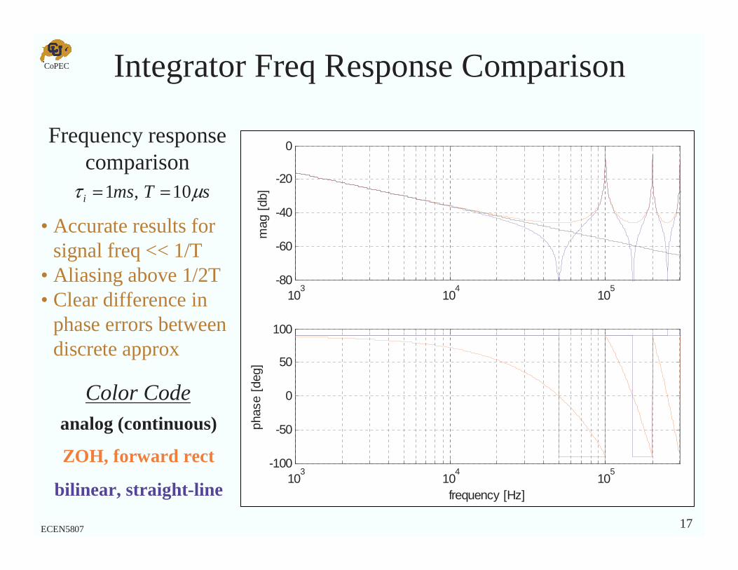
Integrator Freq Response Comparison
• Accurate results for signal freq << 1/T
• Aliasing above 1/2T • Clear difference in
phase errors between discrete approx
sTmsi µτ 10,1 ==
Frequency response comparison
analog (continuous)
bilinear, straight-line
ZOH, forward rect
Color Code
CoPEC
18ECEN5807
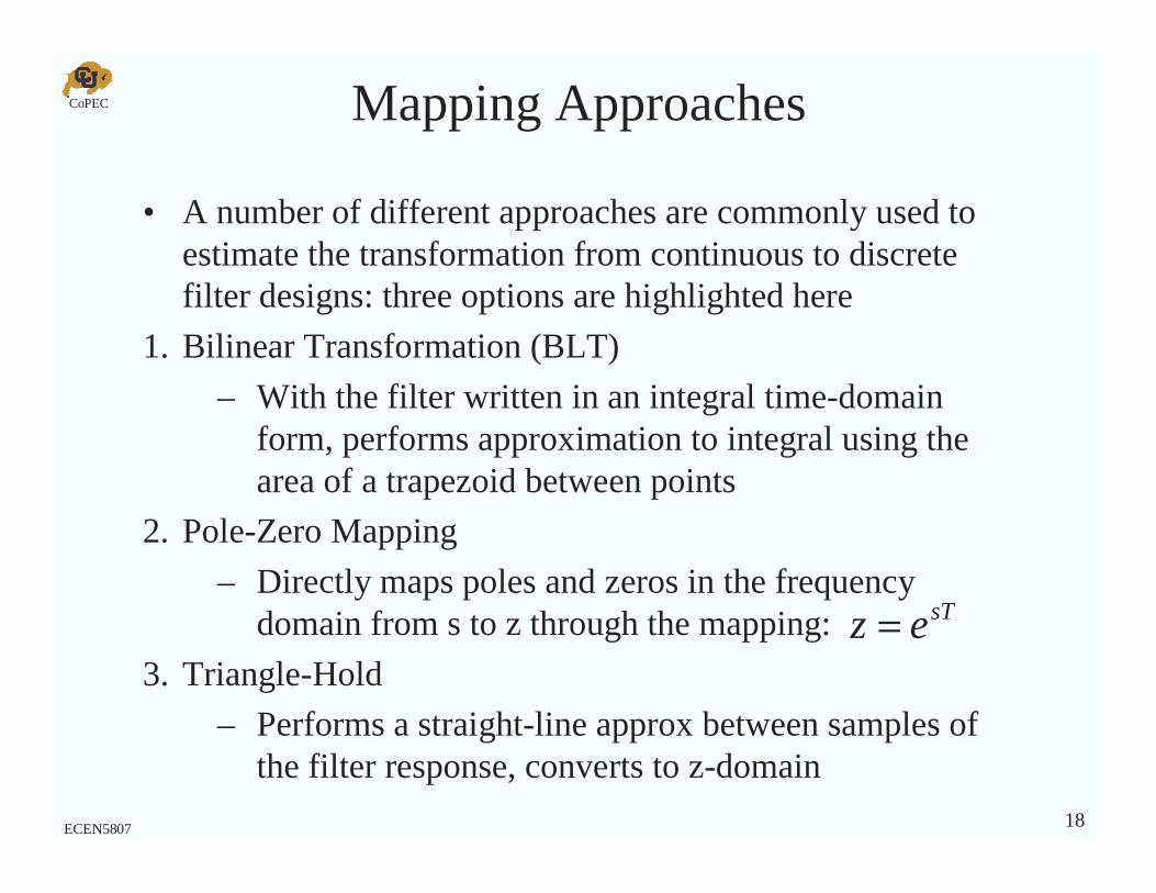
Mapping Approaches
• A number of different approaches are commonly used to estimate the transformation from continuous to discrete filter designs: three options are highlighted here
1. Bilinear Transformation (BLT)
– With the filter written in an integral time-domain form, performs approximation to integral using the area of a trapezoid between points
2. Pole-Zero Mapping
– Directly maps poles and zeros in the frequency domain from s to z through the mapping:
3. Triangle-Hold
– Performs a straight-line approx between samples of the filter response, converts to z-domain
sTez =
CoPEC
19ECEN5807
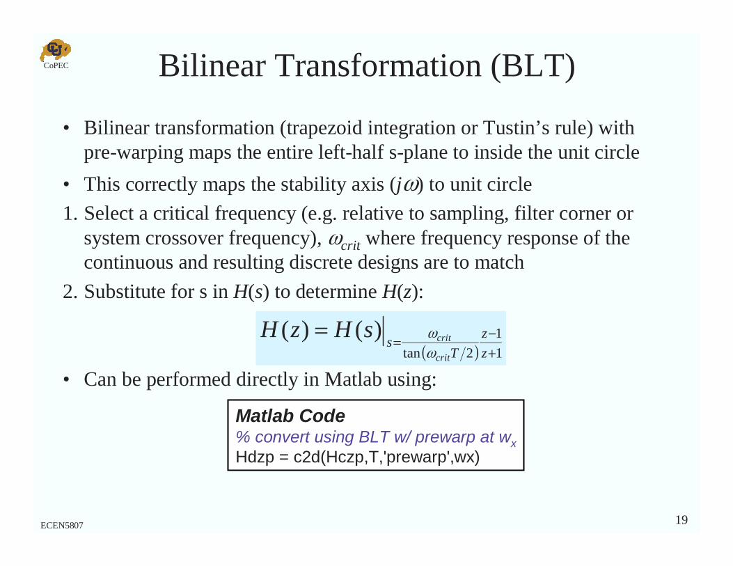
Bilinear Transformation (BLT)
• Bilinear transformation (trapezoid integration or Tustin’s rule) with pre-warping maps the entire left-half s-plane to inside the unit circle
• This correctly maps the stability axis (jω) to unit circle
1. Select a critical frequency (e.g. relative to sampling, filter corner or system crossover frequency), ωcrit where frequency response of the continuous and resulting discrete designs are to match
2. Substitute for s in H(s) to determine H(z):
• Can be performed directly in Matlab using: ( ) 1
1
2tan
)()(+−=
=z
z
Ts
crit
critsHzHωω
Matlab Code% convert using BLT w/ prewarp at wxHdzp = c2d(Hczp,T,'prewarp',wx)
CoPEC
20ECEN5807
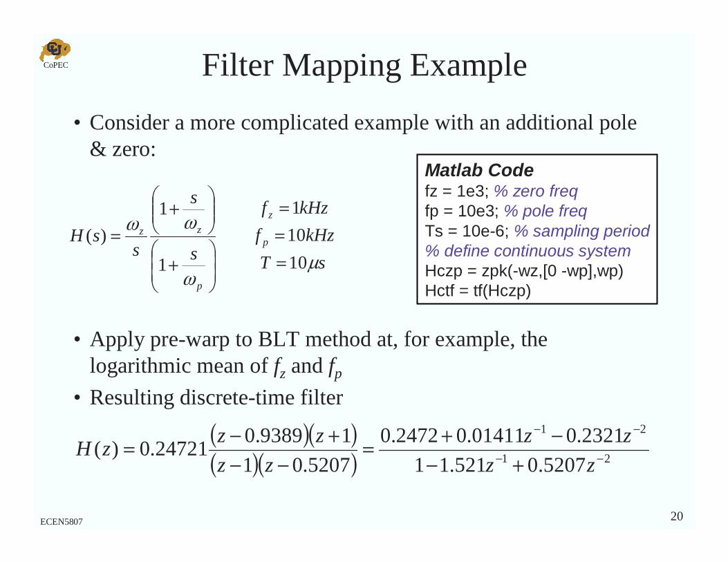
Filter Mapping Example
• Consider a more complicated example with an additional pole & zero:
• Apply pre-warp to BLT method at, for example, the logarithmic mean of fz and fp
• Resulting discrete-time filter
+
+
=
p
zz
s
s
ssH
ω
ωω
1
1
)(
sT
kHzf
kHzf
p
z
µ10
10
1
===
Matlab Codefz = 1e3; % zero freqfp = 10e3; % pole freqTs = 10e-6; % sampling period% define continuous systemHczp = zpk(-wz,[0 -wp],wp)Hctf = tf(Hczp)
( )( )( )( ) 21
21
5207.0521.11
2321.001411.02472.0
5207.01
19389.024721.0)( −−
−−
+−−+=
−−+−=
zz
zz
zz
zzzH
CoPEC
21ECEN5807
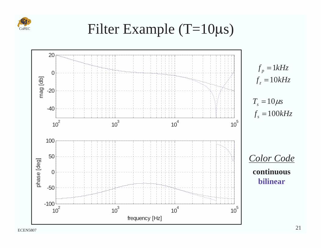
Filter Example (T=10µs)
102
103
104
105
-40
-20
0
20
mag
[db
]
102
103
104
105
-100
-50
0
50
100
phas
e [d
eg]
frequency [Hz]
continuousbilinear
Color Code
kHzf
sT
kHzf
kHzf
s
s
z
p
100
10
10
1
==
==
µ
CoPEC
22ECEN5807
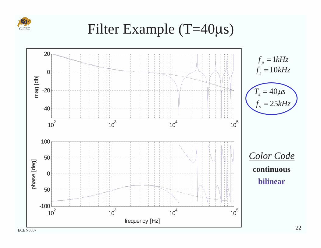
Filter Example (T=40µs)
102
103
104
105
-40
-20
0
20
mag
[db
]
102
103
104
105
-100
-50
0
50
100
phas
e [d
eg]
frequency [Hz]
kHzf
sT
kHzfkHzf
s
s
z
p
25
40
101
==
==
µ
continuous
bilinear
Color Code
CoPEC
23ECEN5807
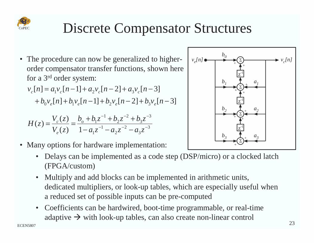
Discrete Compensator Structures
Σ
z-1
Σ
z-1
Σ
z-1
Σ
b0
b1
b2
b3
a1
a2
a3
++
++
+
+ +
+
+
+
ve[n] vc[n]
]3[]2[]1[][
]3[]2[]1[][
3210
321
−+−+−++−+−+−=
nvbnvbnvbnvb
nvanvanvanv
eeee
cccc
33
22
11
33
22
11
1)(
)()( −−−
−−−
−−−+++==
zazaza
zbzbzbb
zV
zVzH o
e
c
• The procedure can now be generalized to higher-order compensator transfer functions, shown here for a 3rd order system:
• Many options for hardware implementation:
• Delays can be implemented as a code step (DSP/micro) or a clocked latch (FPGA/custom)
• Multiply and add blocks can be implemented in arithmetic units, dedicated multipliers, or look-up tables, which are especially useful when a reduced set of possible inputs can be pre-computed
• Coefficients can be hardwired, boot-time programmable, or real-time adaptive with look-up tables, can also create non-linear control
CoPEC
24ECEN5807
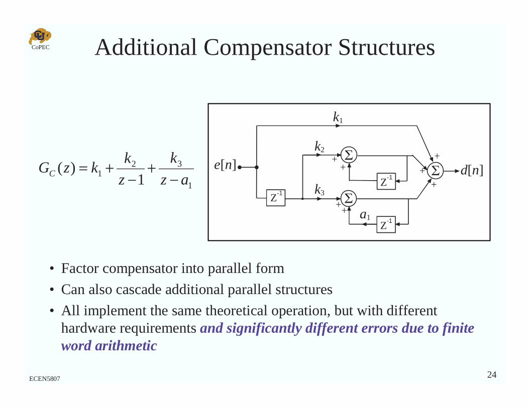
Additional Compensator Structures
• Factor compensator into parallel form
• Can also cascade additional parallel structures
• All implement the same theoretical operation, but with differenthardware requirements and significantly different errors due to finite word arithmetic
1
321 1
)(az
k
z
kkzGC −
+−
+= Σe[n] d[n]k3
k1
k2
Σ++
++
Z-1
Z-1
Σ+
Z-1
+
a1
+
CoPEC
25ECEN5807
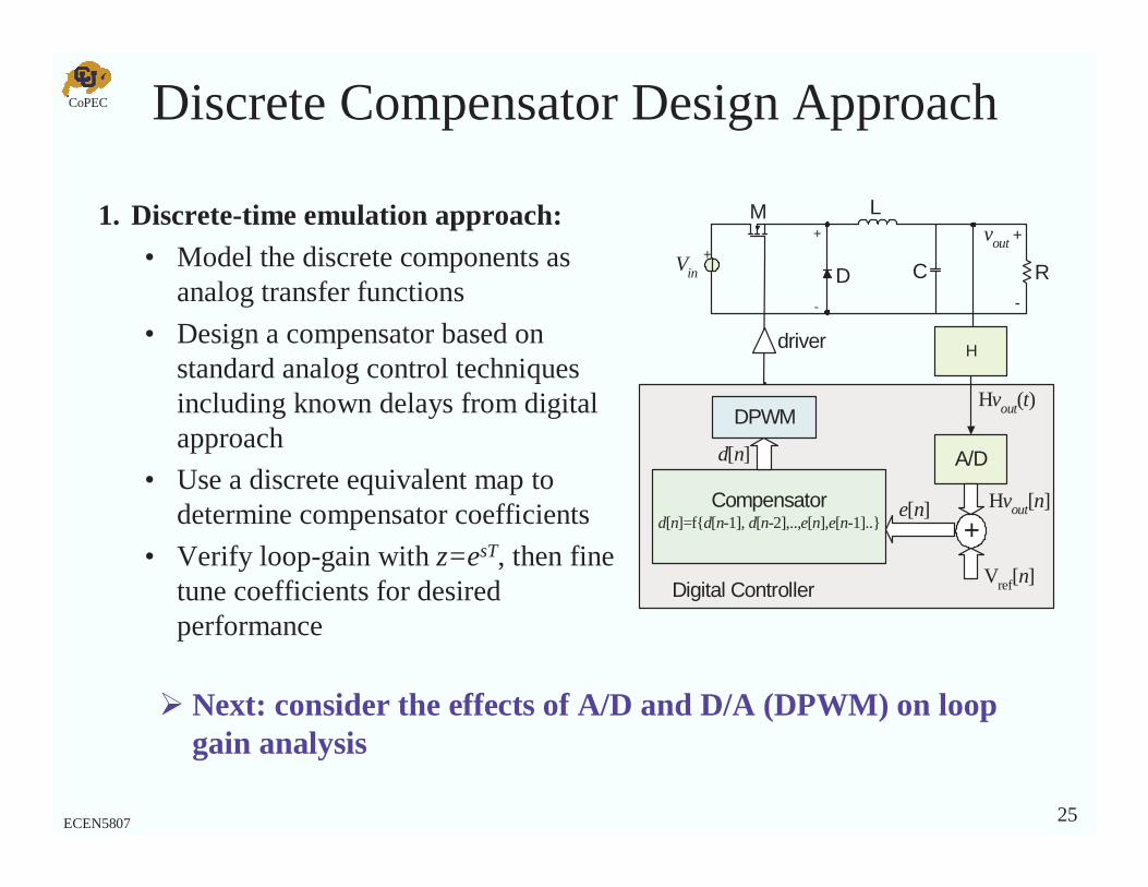
Discrete Compensator Design Approach
H
D
M L
C R
vout+
+
-
A/D
Compensatord[n]=fd[n-1], d[n-2],..,e[n],e[n-1]..
DPWMHvout(t)
Hvout[n]
Digital Controller
e[n]+
Vref[n]
+
-
Vin
driver
d[n]
1. Discrete-time emulation approach:
• Model the discrete components as analog transfer functions
• Design a compensator based on standard analog control techniques including known delays from digital approach
• Use a discrete equivalent map to determine compensator coefficients
• Verify loop-gain with z=esT, then fine tune coefficients for desired performance
Next: consider the effects of A/D and D/A (DPWM) on loop gain analysis
CoPEC
26ECEN5807
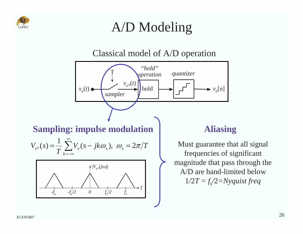
A/D Modeling
TjksVT
sV sk
see πωω 2,)(1
)(* =−= ∑∞
−∞=
fsfs/2f
-fs/2-fs 0
|Ve*(jω)|
Sampling: impulse modulation
Must guarantee that all signal frequencies of significant
magnitude that pass through the A/D are band-limited below
1/2T = fs/2=Nyquist freq
T
ve(t)
quantizer
ve[n]sampler
hold
“hold”operation
ve*(t)
Classical model of A/D operation
Aliasing
CoPEC
27ECEN5807
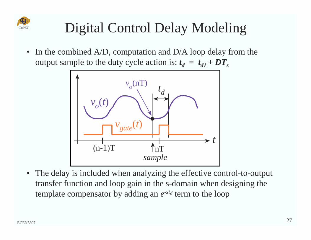
Digital Control Delay Modeling
• In the combined A/D, computation and D/A loop delay from the output sample to the duty cycle action is: td = td1 + DTs
• The delay is included when analyzing the effective control-to-output transfer function and loop gain in the s-domain when designing the template compensator by adding an e-std term to the loop
t
vo(t)
nT
vgate(t)
td
sample(n-1)T
vo(nT)
CoPEC
28ECEN5807
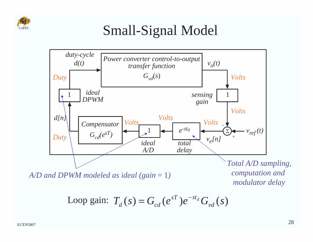
Compensatord[n]
Gcd(esT)
Gvd(s)
Power converter control-to-outputtransfer function vo(t)
duty-cycle
idealA/D
ve[n]vref (t)
d(t)
Σ+
_
1idealDPWM
1
e-std1
sensinggain
totaldelay
)()()( sGeeGsT vdstsT
cddd−=Loop gain:
Total A/D sampling,computation and modulator delay
A/D and DPWM modeled as ideal (gain = 1)
Volts
Volts
VoltsVolts
Duty
Duty
Volts
Small-Signal Model
CoPEC
29ECEN5807
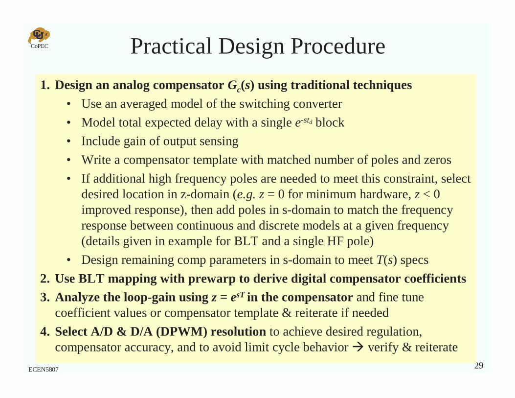
Practical Design Procedure
1. Design an analog compensator Gc(s) using traditional techniques
• Use an averaged model of the switching converter
• Model total expected delay with a single e-std block
• Include gain of output sensing
• Write a compensator template with matched number of poles and zeros
• If additional high frequency poles are needed to meet this constraint, select desired location in z-domain (e.g. z = 0 for minimum hardware, z < 0 improved response), then add poles in s-domain to match the frequency response between continuous and discrete models at a given frequency (details given in example for BLT and a single HF pole)
• Design remaining comp parameters in s-domain to meet T(s) specs
2. Use BLT mapping with prewarp to derive digital compensator coefficients3. Analyze the loop-gain using z = esT in the compensator and fine tune
coefficient values or compensator template & reiterate if needed
4. Select A/D & D/A (DPWM) resolution to achieve desired regulation, compensator accuracy, and to avoid limit cycle behavior verify & reiterate
CoPEC
30ECEN5807
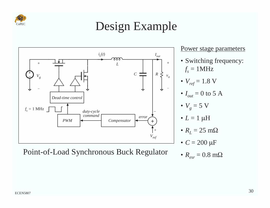
Design Example
+–
L
iL(t)
+
Vg
_
+
vo
_
Vref
C
Dead-time control
+
_
+PWM Compensator
fs = 1 MHz
errorduty-cyclecommand
Iout
R
Power stage parameters
• Switching frequency: fs = 1MHz
• Vref = 1.8 V
• Iout = 0 to 5 A
• Vg = 5 V
• L = 1 µH
• RL = 25 mΩ
• C = 200 µF
• Resr = 0.8 mΩPoint-of-Load Synchronous Buck Regulator
CoPEC
31ECEN5807
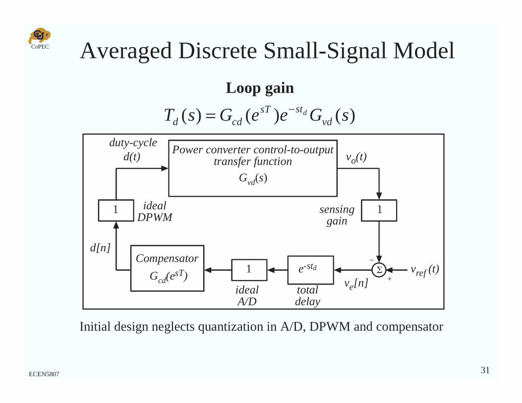
Averaged Discrete Small-Signal Model
Initial design neglects quantization in A/D, DPWM and compensator
Loop gain
Compensatord[n]
Gcd(esT)
Gvd(s)
Power converter control-to-outputtransfer function vo(t)
duty-cycle
idealA/D
ve[n]vref (t)
d(t)
Σ+
_
1idealDPWM
1
e-std1
sensinggain
totaldelay
)()()( sGeeGsT vdstsT
cddd−=
CoPEC
32ECEN5807
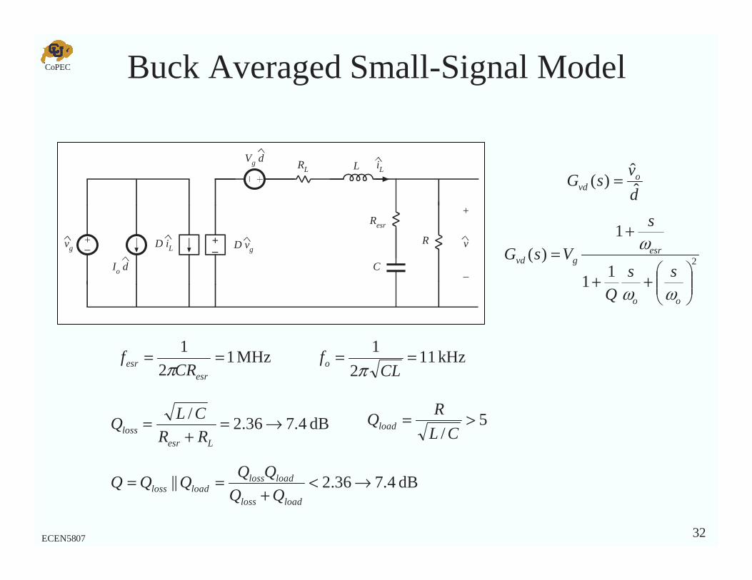
Buck Averaged Small-Signal Model
+–
L
C
R
+
v
–
vg+–
D vg
Vg d
Io d
D iL
iL
Resr
RL
21
1
1)(
++
+=
oo
esrgvd
ss
Q
s
VsG
ωω
ω
MHz 12
1 ==esr
esr CRf
πkHz 11
2
1 ==CL
fo π
dB 4.736.2/ →=+
=Lesr
loss RR
CLQ 5
/>=
CL
RQload
dB 4.736.2|| →<+
==loadloss
loadlossloadloss QQ
QQQQQ
d
vsG o
vd ˆˆ
)( =
CoPEC
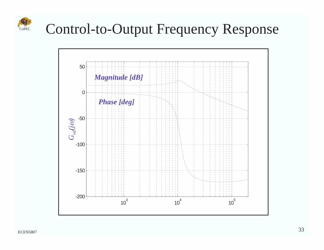
33ECEN5807
103
104
105
-200
-150
-100
-50
0
50
Control-to-Output Frequency Response
Magnitude [dB]
Phase [deg]
Gvd
(jω)
CoPEC
34ECEN5807
102
103
104
105
106
-300
-250
-200
-150
-100
-50
0
50
frequency [Hz]
Uncompensated Loop Gain with Delays
Magnitude [dB]
Phase [deg]
)()( sGesT vdst
ud−= sTs µ1=
td = 1µstd = 360ns
td = 0
• Recall td models delay from sample point to falling edge of PWM
• Next, select and design analog compensator template
td = 200ns
CoPEC
35ECEN5807
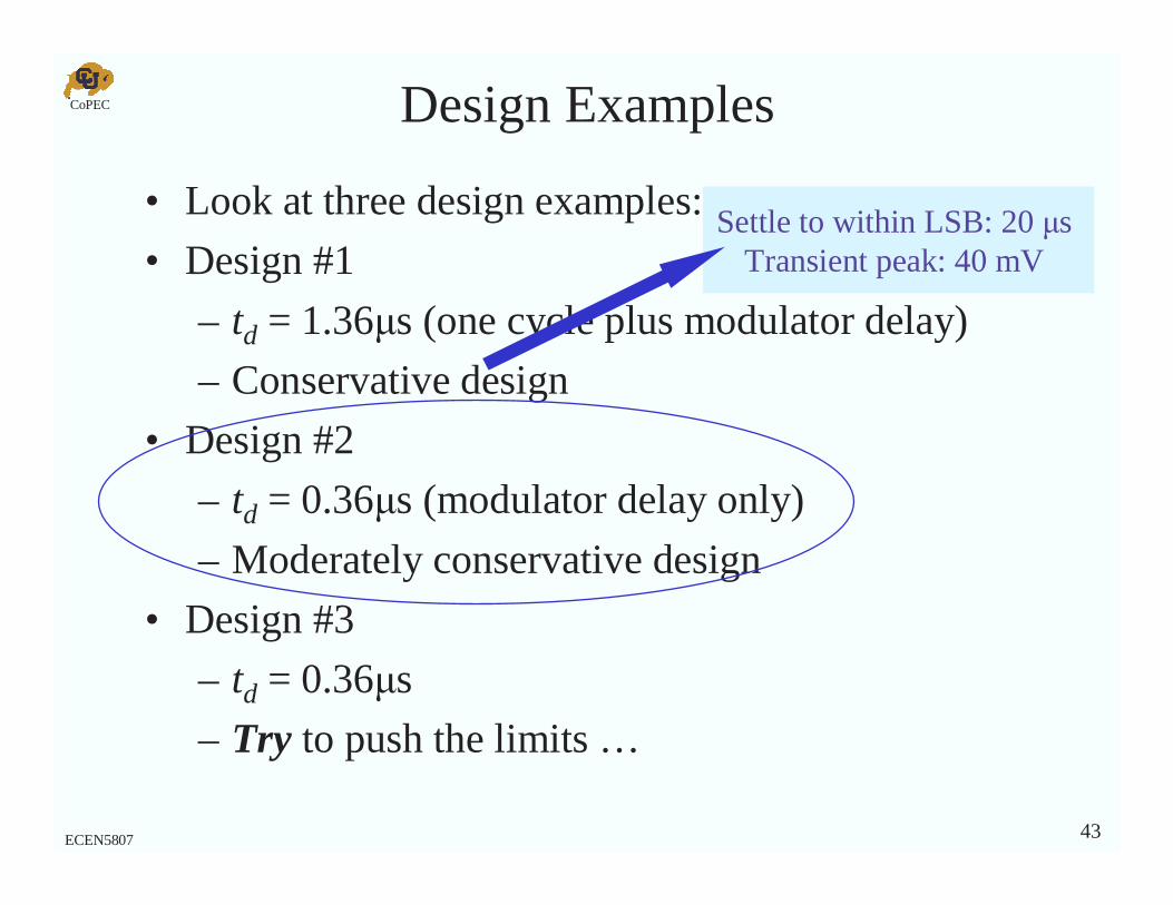
Design Examples
• Look at three design examples:
• Design #1
– td = 1.36µs (one cycle plus modulator delay)
– Conservative design
• Design #2
– td = 0.36µs (modulator delay only)
– Moderately conservative design
• Design #3
– td = 0.36µs
– Try to push the limits …
CoPEC
36ECEN5807
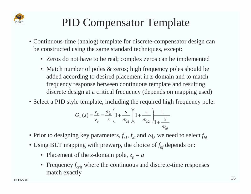
• Continuous-time (analog) template for discrete-compensator design can be constructed using the same standard techniques, except:
• Zeros do not have to be real; complex zeros can be implemented
• Match number of poles & zeros; high frequency poles should be added according to desired placement in z-domain and to match frequency response between continuous template and resulting discrete design at a critical frequency (depends on mapping used)
• Select a PID style template, including the required high frequency pole:
PID Compensator Template
hf
zz
k
o
cct s
ss
sv
vsG
ωωω
ω
+
+
+==
1
111)(
21
• Prior to designing key parameters, fz1, fz1 and ωk, we need to select fhf
• Using BLT mapping with prewarp, the choice of fhf depends on:
• Placement of the z-domain pole, zp = a
• Frequency fcrit where the continuous and discrete-time responses match exactly
CoPEC
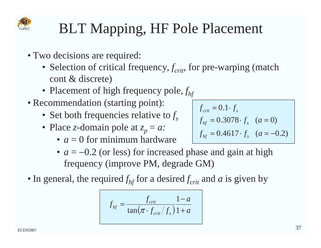
37ECEN5807
• Two decisions are required:• Selection of critical frequency, fcrit, for pre-warping (match
cont & discrete)• Placement of high frequency pole, fhf
• Recommendation (starting point):• Set both frequencies relative to fs
• Place z-domain pole at zp = a:• a = 0 for minimum hardware• a = −0.2 (or less) for increased phase and gain at high
frequency (improve PM, degrade GM)
• In general, the required fhf for a desired fcrit and a is given by
BLT Mapping, HF Pole Placement
)2.0(4617.0
)0(3078.0
1.0
−=⋅=
=⋅=⋅=
aff
aff
ff
shf
shf
scrit
( ) a
a
ff
ff
scrit
crithf +
−⋅
=1
1
tan π
CoPEC
38ECEN5807
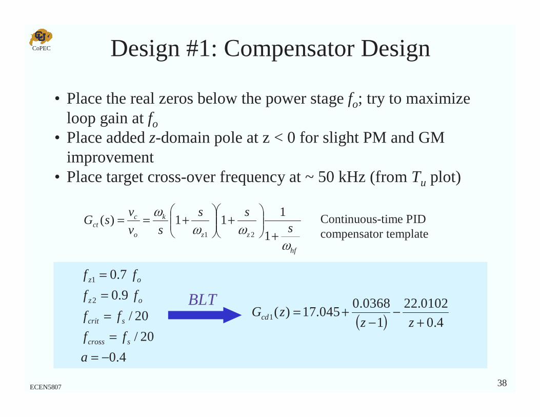
Design #1: Compensator Design
4.0
20/
20/
9.0
7.0
2
1
−=====
a
ff
ff
ff
ff
scross
scrit
oz
oz
( ) 4.0
0102.22
1
0368.0045.17)(1 +
−−
+=zz
zGcd
• Place the real zeros below the power stage fo; try to maximize loop gain at fo
• Place added z-domain pole at z < 0 for slight PM and GM improvement
• Place target cross-over frequency at ~ 50 kHz (from Tu plot)
BLT
hf
zz
k
o
cct s
ss
sv
vsG
ωωω
ω
+
+
+==
1
111)(
21
Continuous-time PID compensator template
CoPEC
39ECEN5807
Design #1: Loop Gain Response
Template Design
Discrete Design103
104
105
106
-40
-20
0
20
40
60
80Template (black), Discrete (blue) and Discrete Rounded (red) Loop Gain
mag
nitu
de [
db]
103
104
105
106
-250
-200
-150
-100
-50
0
frequency [Hz]
phas
e [d
eg]
Resultsfc = 50 kHz
PM = 49 degGM = 10.4 dB
td = 1.36µs
CoPEC
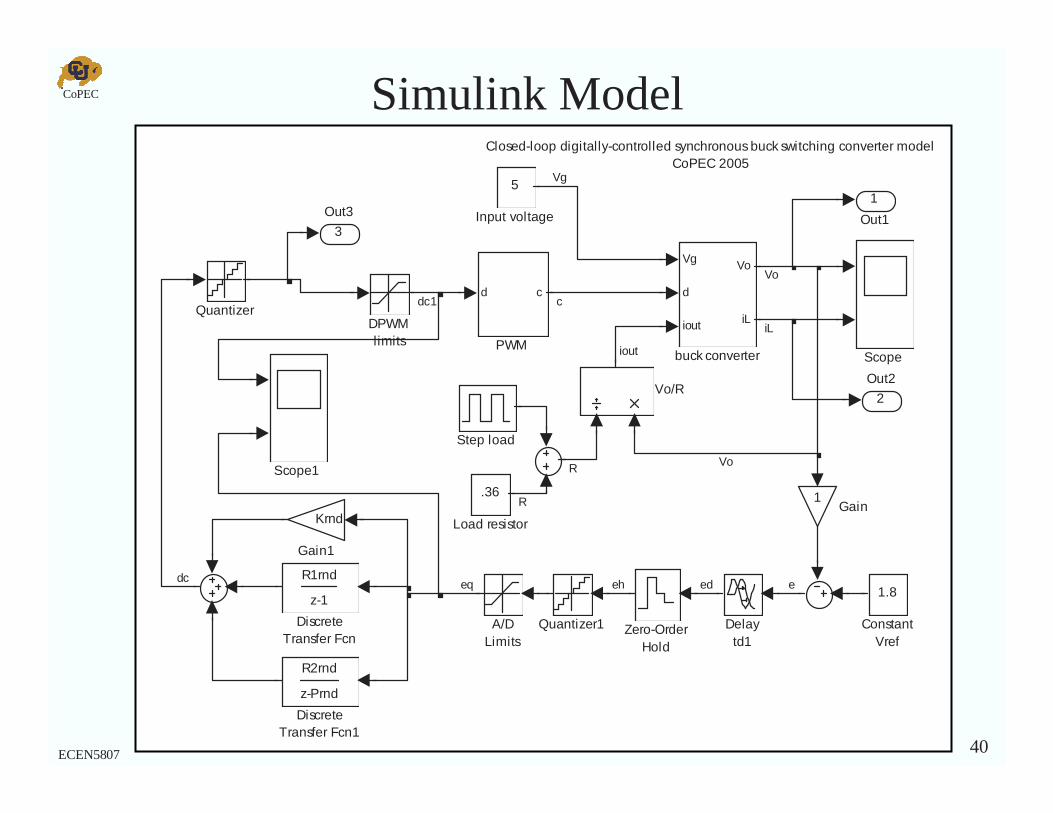
40ECEN5807
Simulink ModelClosed-loop digitally-controlled synchronous buck switching converter model
CoPEC 2005
3
Out3
2
Out2
1
Out1
Vg
d
iout
Vo
iL
buck converter
Zero-OrderHold
Vo/R
Step load
Scope1
Scope
Quantizer1
Quantizerd c
PWM
.36
Load resistor
5
Input voltage
Krnd
Gain1
1Gain
R2rnd
z-Prnd
DiscreteTransfer Fcn1
R1rnd
z-1
DiscreteTransfer Fcn
Delaytd1
DPWMlimits
1.8
ConstantVref
A/DLimits
Vg
Vo
Vo
iL
iout
R
R
dc1
ed eeq ehdc
c
CoPEC
41ECEN5807
4.8 5 5.2 5.4 5.6 5.8 6 6.2 6.4 6.6 6.8
x 10-4
1.75
1.8
1.85
4.8 5 5.2 5.4 5.6 5.8 6 6.2 6.4 6.6 6.8
x 10-4
0
2
4
6
8
4.8 5 5.2 5.4 5.6 5.8 6 6.2 6.4 6.6 6.8
x 10-4
0
0.2
0.4
0.6
0.8
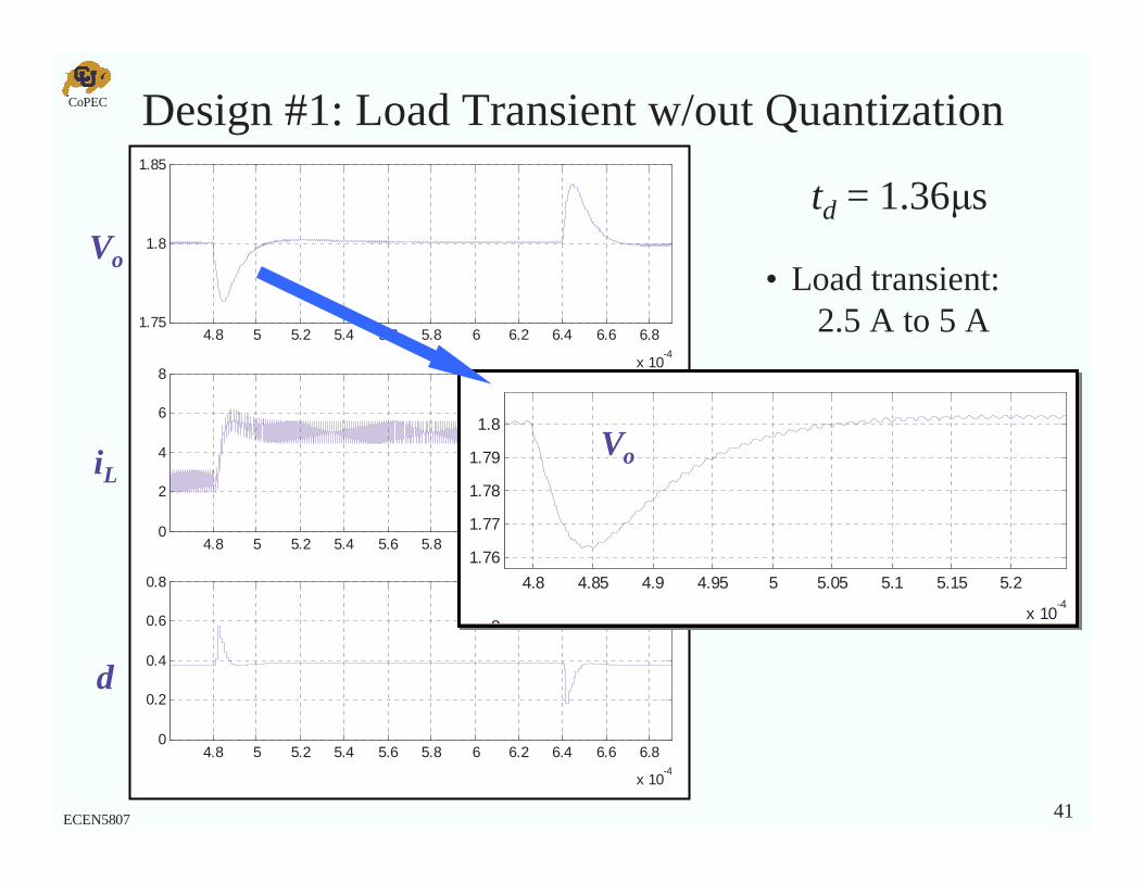
Design #1: Load Transient w/out Quantization
Vo
iL
d
• Load transient:2.5 A to 5 A
4.8 4.85 4.9 4.95 5 5.05 5.1 5.15 5.2
x 10-4
1.76
1.77
1.78
1.79
1.8
8
4.8 4.85 4.9 4.95 5 5.05 5.1 5.15 5.2
x 10-4
1.76
1.77
1.78
1.79
1.8
8
Vo
td = 1.36µs
CoPEC
42ECEN5807
4.8 5 5.2 5.4 5.6 5.8 6 6.2 6.4 6.6 6.8
x 10-4
1.75
1.8
1.85
4.8 5 5.2 5.4 5.6 5.8 6 6.2 6.4 6.6 6.8
x 10-4
0
2
4
6
8
4.8 5 5.2 5.4 5.6 5.8 6 6.2 6.4 6.6 6.8
x 10-4
0
0.2
0.4
0.6
0.8
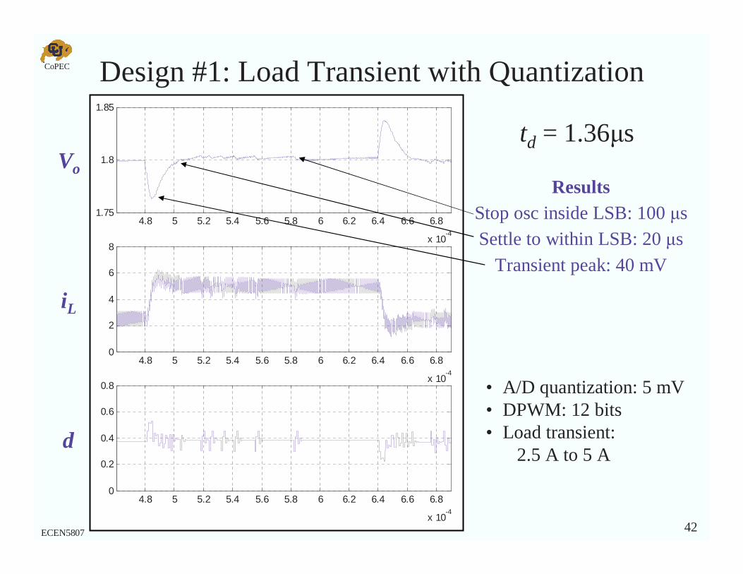
Design #1: Load Transient with Quantization
Vo
iL
d
• A/D quantization: 5 mV• DPWM: 12 bits• Load transient:
2.5 A to 5 A
ResultsStop osc inside LSB: 100 µsSettle to within LSB: 20 µs
Transient peak: 40 mV
td = 1.36µs
CoPEC
43ECEN5807
Design Examples
• Look at three design examples:
• Design #1
– td = 1.36µs (one cycle plus modulator delay)
– Conservative design
• Design #2
– td = 0.36µs (modulator delay only)
– Moderately conservative design
• Design #3
– td = 0.36µs
– Try to push the limits …
Settle to within LSB: 20 µsTransient peak: 40 mV
CoPEC
44ECEN5807
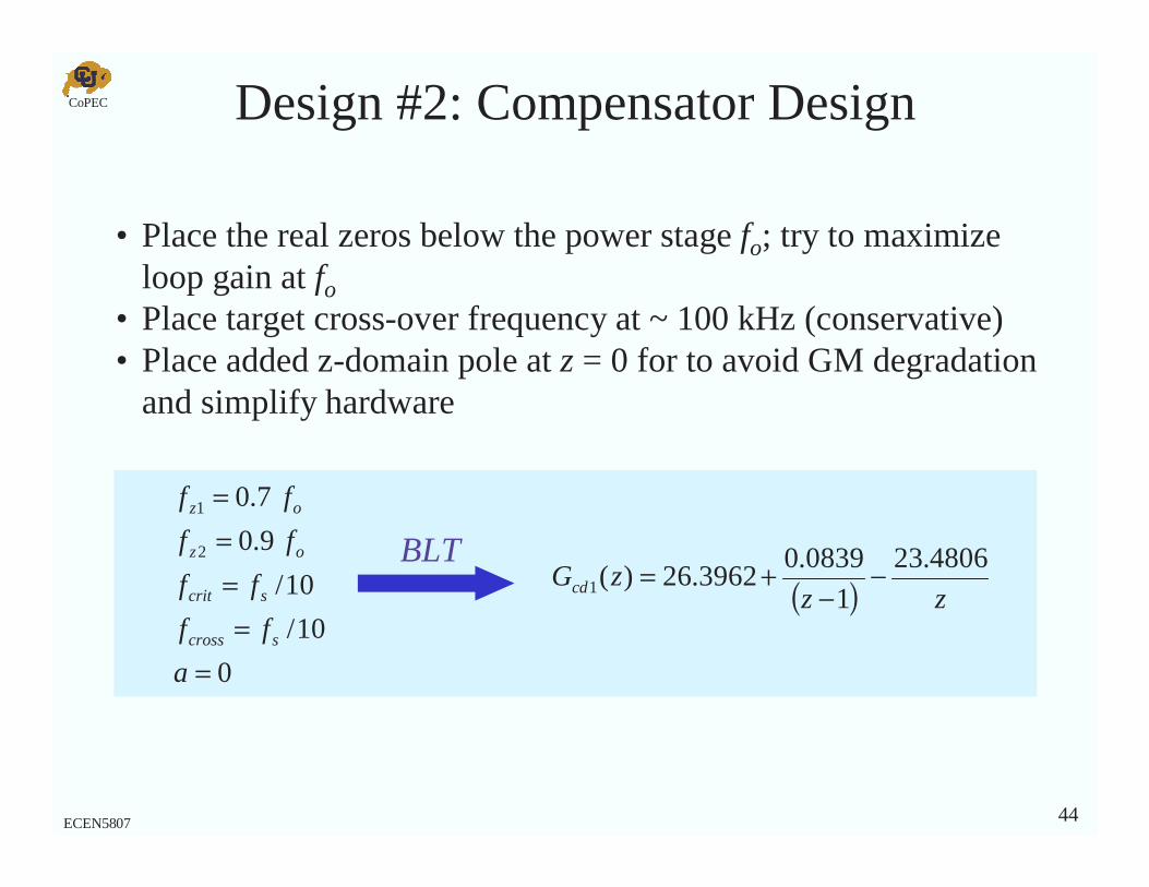
Design #2: Compensator Design
0
10/
10/
9.0
7.0
2
1
=====
a
ff
ff
ff
ff
scross
scrit
oz
oz
( ) zzzGcd
4806.23
1
0839.03962.26)(1 −
−+=
• Place the real zeros below the power stage fo; try to maximize loop gain at fo
• Place target cross-over frequency at ~ 100 kHz (conservative)• Place added z-domain pole at z = 0 for to avoid GM degradation
and simplify hardware
BLT
CoPEC
45ECEN5807
103
104
105
106
-40
-20
0
20
40
60
80Template (black), Discrete (blue) and Discrete Rounded (red) Loop Gain
mag
nitu
de [
db]
103
104
105
106
-250
-200
-150
-100
-50
0
frequency [Hz]
phas
e [d
eg]
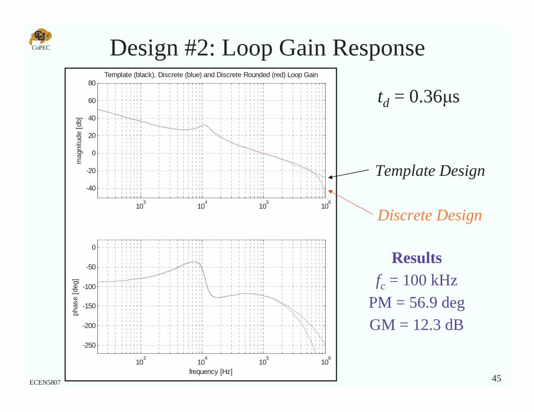
Design #2: Loop Gain Response
Template Design
Discrete Design
Resultsfc = 100 kHz
PM = 56.9 degGM = 12.3 dB
td = 0.36µs
CoPEC
46ECEN5807
4.8 5 5.2 5.4 5.6 5.8 6 6.2 6.4 6.6 6.8
x 10-4
1.75
1.8
1.85
4.8 5 5.2 5.4 5.6 5.8 6 6.2 6.4 6.6 6.8
x 10-4
0
2
4
6
8
4.8 5 5.2 5.4 5.6 5.8 6 6.2 6.4 6.6 6.8
x 10-4
0
0.2
0.4
0.6
0.8
4.8 4.85 4.9 4.95 5 5.05 5.1 5.15 5.2
x 10-4
1.76
1.77
1.78
1.79
1.8
8
4.8 4.85 4.9 4.95 5 5.05 5.1 5.15 5.2
x 10-4
1.76
1.77
1.78
1.79
1.8
8
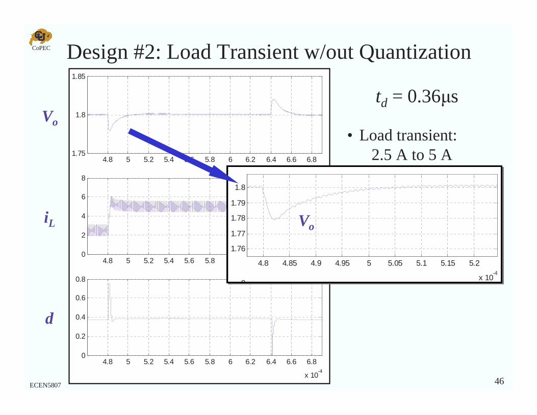
Design #2: Load Transient w/out Quantization
Vo
iL
d
• Load transient:2.5 A to 5 A
td = 0.36µs
Vo
CoPEC
47ECEN5807
4.8 5 5.2 5.4 5.6 5.8 6 6.2 6.4 6.6 6.8
x 10-4
1.75
1.8
1.85
4.8 5 5.2 5.4 5.6 5.8 6 6.2 6.4 6.6 6.8
x 10-4
0
2
4
6
8
4.8 5 5.2 5.4 5.6 5.8 6 6.2 6.4 6.6 6.8
x 10-4
0
0.2
0.4
0.6
0.8
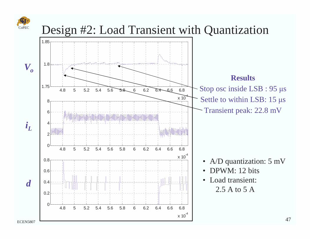
Design #2: Load Transient with Quantization
Vo
iL
d
• A/D quantization: 5 mV• DPWM: 12 bits• Load transient:
2.5 A to 5 A
ResultsStop osc inside LSB : 95 µsSettle to within LSB: 15 µsTransient peak: 22.8 mV
CoPEC
48ECEN5807
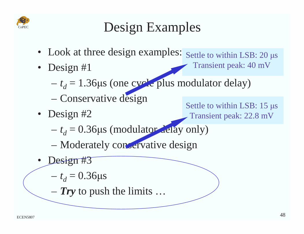
Design Examples
• Look at three design examples:
• Design #1
– td = 1.36µs (one cycle plus modulator delay)
– Conservative design
• Design #2
– td = 0.36µs (modulator delay only)
– Moderately conservative design
• Design #3
– td = 0.36µs
– Try to push the limits …
Settle to within LSB: 20 µsTransient peak: 40 mV
Settle to within LSB: 15 µsTransient peak: 22.8 mV
CoPEC
49ECEN5807
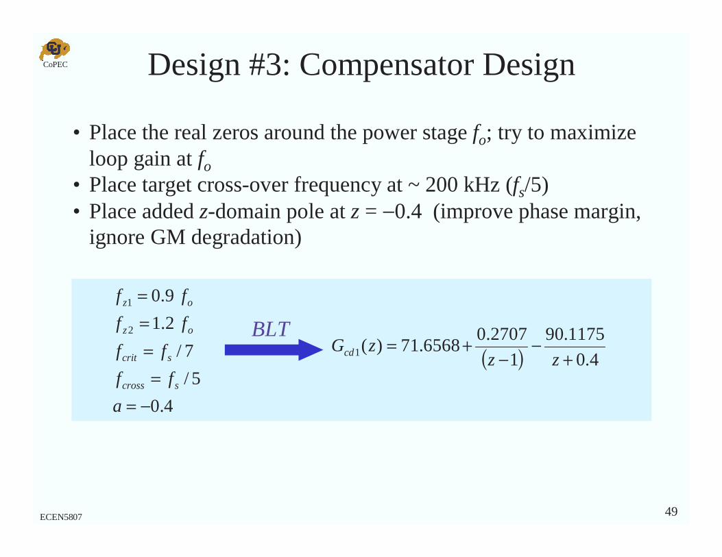
Design #3: Compensator Design
4.0
5/
7/
2.1
9.0
2
1
−=====
a
ff
ff
ff
ff
scross
scrit
oz
oz
( ) 4.0
1175.90
1
2707.06568.71)(1 +
−−
+=zz
zGcd
• Place the real zeros around the power stage fo; try to maximize loop gain at fo
• Place target cross-over frequency at ~ 200 kHz (fs/5)• Place added z-domain pole at z = −0.4 (improve phase margin,
ignore GM degradation)
BLT
CoPEC
50ECEN5807
103
104
105
106
-40
-20
0
20
40
60
80Template (black), Discrete (blue) and Discrete Rounded (red) Loop Gain
mag
nitu
de [
db]
103
104
105
106
-250
-200
-150
-100
-50
0
frequency [Hz]
phas
e [d
eg]
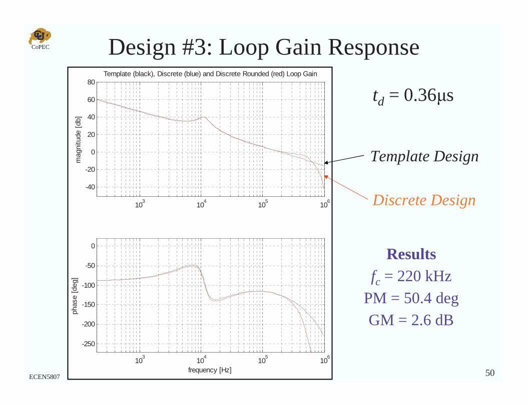
Design #3: Loop Gain Response
Template Design
Discrete Design
Resultsfc = 220 kHz
PM = 50.4 degGM = 2.6 dB
td = 0.36µs
CoPEC
51ECEN5807
4.8 5 5.2 5.4 5.6 5.8 6 6.2 6.4 6.6 6.8
x 10-4
1.75
1.8
1.85
4.8 5 5.2 5.4 5.6 5.8 6 6.2 6.4 6.6 6.8
x 10-4
0
2
4
6
8
4.8 5 5.2 5.4 5.6 5.8 6 6.2 6.4 6.6 6.8
x 10-4
0
0.2
0.4
0.6
0.84.8 4.85 4.9 4.95 5 5.05 5.1 5.15 5.2
x 10-4
1.76
1.77
1.78
1.79
1.8
8
4.8 4.85 4.9 4.95 5 5.05 5.1 5.15 5.2
x 10-4
1.76
1.77
1.78
1.79
1.8
8
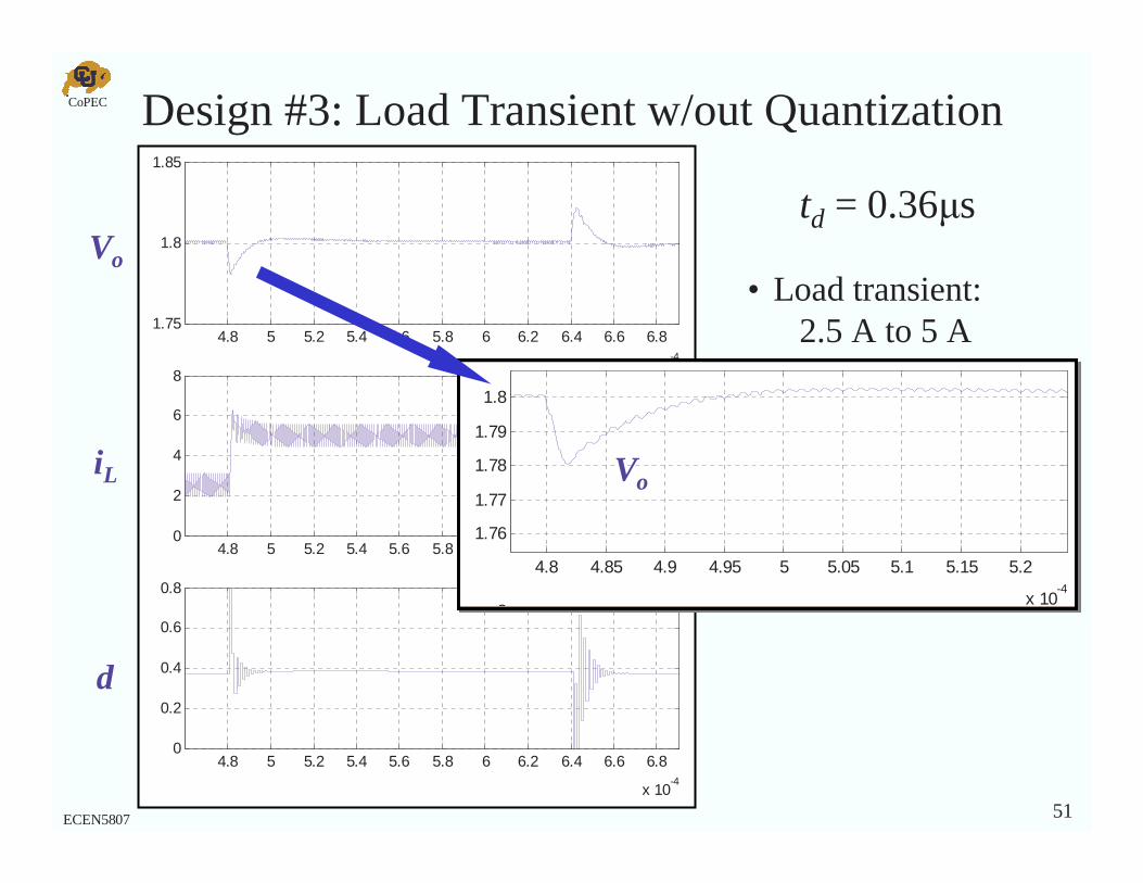
Design #3: Load Transient w/out Quantization
Vo
iL
d
• Load transient:2.5 A to 5 A
Vo
td = 0.36µs
CoPEC
52ECEN5807
4.8 5 5.2 5.4 5.6 5.8 6 6.2 6.4 6.6 6.8
x 10-4
1.75
1.8
1.85
4.8 5 5.2 5.4 5.6 5.8 6 6.2 6.4 6.6 6.8
x 10-4
0
2
4
6
8
4.8 5 5.2 5.4 5.6 5.8 6 6.2 6.4 6.6 6.8
x 10-4
0
0.2
0.4
0.6
0.8
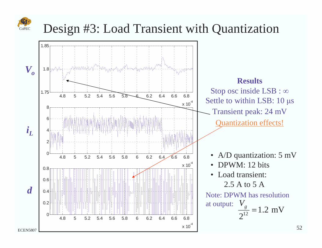
Design #3: Load Transient with Quantization
Vo
iL
d
• A/D quantization: 5 mV• DPWM: 12 bits• Load transient:
2.5 A to 5 A
ResultsStop osc inside LSB : ∞
Settle to within LSB: 10 µsTransient peak: 24 mVQuantization effects!
Note: DPWM has resolutionat output:
mV2.1212 =
gV
CoPEC
53ECEN5807
Settle to within LSB: 10 µsTransient peak: 24 mV
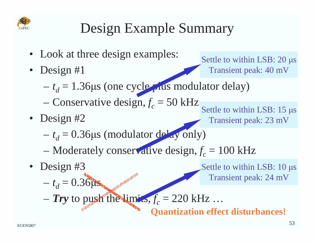
Design Example Summary
• Look at three design examples:
• Design #1
– td = 1.36µs (one cycle plus modulator delay)
– Conservative design, fc = 50 kHz
• Design #2
– td = 0.36µs (modulator delay only)
– Moderately conservative design, fc = 100 kHz
• Design #3
– td = 0.36µs
– Try to push the limits, fc = 220 kHz …
Settle to within LSB: 20 µsTransient peak: 40 mV
Settle to within LSB: 15 µsTransient peak: 23 mV
Quantization effect disturbances!