Embed Size (px)
Citation preview

Digital Semiconductor 21164Alpha Microprocessor MotherboardUser’s ManualOrder Number: EC–QLJLC–TE
Revision/Update Information: This document supersedes theAlpha 21164 Microprocessor MotherboardUser’s Manual (EC–QLJLB–TE).
Digital Equipment CorporationMaynard, Massachusetts

March 1996
Possession, use, or copying of the software described in this publication is authorized onlypursuant to a valid written license from Digital or an authorized sublicensor.
While Digital believes the information included in this publication is correct as of the date ofpublication, it is subject to change without notice.
Digital Equipment Corporation makes no representations that the use of its products in themanner described in this publication will not infringe on existing or future patent rights, nor dothe descriptions contained in this publication imply the granting of licenses to make, use, or sellequipment or software in accordance with the description.
© Digital Equipment Corporation 1996.
All rights reserved.Printed in U.S.A.
Alpha AXP, AlphaGeneration, DEC, DECchip, DECladebug, Digital, Digital Semiconductor,OpenVMS, VAX, VAX DOCUMENT, VMS, the AlphaGeneration design mark, and theDIGITAL logo are trademarks of Digital Equipment Corporation.
Digital Semiconductor is a Digital Equipment Corporation business.Digital UNIX Version 3.2 for Alpha is a UNIX 93 branded product.
Centronics is a trademark of Genicom Corporation.CompuServe is a registered trademark of CompuServe, Inc.FaxBACK is a registered trademark and Intel and UPI are trademarks of Intel Corporation.GRAFOIL is a registered trademark of Union Carbide Corporation.IEEE is a registered trademark of The Institute of Electrical and Electronics Engineers, Inc.MACH is a trademark of Advanced Micro Devices, Inc.Micron is a registered trademark of Micron Corporation.Microsoft is a registered trademark and NT and Windows NT are trademarks of MicrosoftCorporation.Motorola is a registered trademark of Motorola, Inc.National is a registered trademark of National Semiconductor Corporation.PS/2 is a registered trademark of International Business Machines Corporation.SPEC is a trademark of Standard Performance Evaluation Corporation.TriQuint is a registered trademark of TriQuint Semiconductor, Inc.UNIX is a registered trademark in the United States and other countries, licensed exclusivelythrough X/Open Company Ltd.Xilinx is a trademark of Xilinx, Incorporated.
All other trademarks and registered trademarks are the property of their respective owners.
This document was prepared using VAX DOCUMENT Version 2.1.
Contents
About This Manual . . . . . . . . . . . . . . . . . . . . . . . . . . . . . . . . . . . . . . . . . . . vii
1 Introduction to the EB164
1.1 System Components and Features . . . . . . . . . . . . . . . . . . . . . . . . 1–11.1.1 Digital Semiconductor 21171 Core Logic Chipset . . . . . . . . . . 1–11.1.2 Memory Subsystem . . . . . . . . . . . . . . . . . . . . . . . . . . . . . . . . 1–31.1.3 L3 Bcache Subsystem Overview . . . . . . . . . . . . . . . . . . . . . . . 1–31.1.4 PCI Interface Overview . . . . . . . . . . . . . . . . . . . . . . . . . . . . . 1–31.1.5 ISA Interface Overview . . . . . . . . . . . . . . . . . . . . . . . . . . . . . 1–41.1.6 Miscellaneous Logic . . . . . . . . . . . . . . . . . . . . . . . . . . . . . . . . 1–41.1.7 Software Support . . . . . . . . . . . . . . . . . . . . . . . . . . . . . . . . . . 1–51.1.8 Component Layout . . . . . . . . . . . . . . . . . . . . . . . . . . . . . . . . . 1–51.2 EB164 Summary . . . . . . . . . . . . . . . . . . . . . . . . . . . . . . . . . . . . . 1–6
2 System Configuration and Connectors
2.1 Configuration Jumpers . . . . . . . . . . . . . . . . . . . . . . . . . . . . . . . . . 2–12.2 EB164 Connectors . . . . . . . . . . . . . . . . . . . . . . . . . . . . . . . . . . . . 2–8
3 Starting and Using the EB164
3.1 Hardware Requirements . . . . . . . . . . . . . . . . . . . . . . . . . . . . . . . 3–13.2 Software Requirements . . . . . . . . . . . . . . . . . . . . . . . . . . . . . . . . 3–23.3 Hardware Configuration . . . . . . . . . . . . . . . . . . . . . . . . . . . . . . . 3–23.4 Software Configuration . . . . . . . . . . . . . . . . . . . . . . . . . . . . . . . . 3–83.4.1 Starting Windows NT ARC Firmware . . . . . . . . . . . . . . . . . . 3–93.4.2 Going to the Debug Monitor from Windows NT ARC
Firmware . . . . . . . . . . . . . . . . . . . . . . . . . . . . . . . . . . . . . . . . 3–93.4.3 Returning to Windows NT ARC Firmware from the Debug
Monitor . . . . . . . . . . . . . . . . . . . . . . . . . . . . . . . . . . . . . . . . . 3–10
iii

4 Functional Description
4.1 PCI Interrupts and Arbitration . . . . . . . . . . . . . . . . . . . . . . . . . . 4–14.1.1 Interrupts . . . . . . . . . . . . . . . . . . . . . . . . . . . . . . . . . . . . . . . 4–14.1.2 Arbitration . . . . . . . . . . . . . . . . . . . . . . . . . . . . . . . . . . . . . . . 4–54.2 ISA Bus Devices . . . . . . . . . . . . . . . . . . . . . . . . . . . . . . . . . . . . . . 4–54.3 dc Power Distribution . . . . . . . . . . . . . . . . . . . . . . . . . . . . . . . . . 4–54.4 PCI Devices . . . . . . . . . . . . . . . . . . . . . . . . . . . . . . . . . . . . . . . . . 4–74.5 Flash ROM . . . . . . . . . . . . . . . . . . . . . . . . . . . . . . . . . . . . . . . . . . 4–84.5.1 Special ROM Header . . . . . . . . . . . . . . . . . . . . . . . . . . . . . . . 4–84.5.2 Flash ROM Structure . . . . . . . . . . . . . . . . . . . . . . . . . . . . . . . 4–114.5.3 Flash ROM Access . . . . . . . . . . . . . . . . . . . . . . . . . . . . . . . . . 4–13
5 EB164 Requirements, Power, and Parameters
5.1 Power Requirements . . . . . . . . . . . . . . . . . . . . . . . . . . . . . . . . . . 5–15.2 Environmental Requirements . . . . . . . . . . . . . . . . . . . . . . . . . . . 5–25.3 Physical Board Parameters . . . . . . . . . . . . . . . . . . . . . . . . . . . . . 5–2
A Supporting Vendor Products
A.1 Products Included . . . . . . . . . . . . . . . . . . . . . . . . . . . . . . . . . . . . A–1A.2 Products Not Included . . . . . . . . . . . . . . . . . . . . . . . . . . . . . . . . . A–2
B Technical Support and Ordering Information
B.1 Obtaining Technical Support . . . . . . . . . . . . . . . . . . . . . . . . . . . . B–1B.2 Ordering Digital Semiconductor Products . . . . . . . . . . . . . . . . . . B–1B.3 Ordering Digital Semiconductor Literature . . . . . . . . . . . . . . . . . B–2B.4 Ordering Third-Party Literature . . . . . . . . . . . . . . . . . . . . . . . . . B–3
Index
Figures
1–1 EB164 Functional Block Diagram . . . . . . . . . . . . . . . . . . . . . 1–21–2 Board Component Layout . . . . . . . . . . . . . . . . . . . . . . . . . . . 1–62–1 EB164 Jumper Locations . . . . . . . . . . . . . . . . . . . . . . . . . . . . 2–22–2 Configuration Jumpers . . . . . . . . . . . . . . . . . . . . . . . . . . . . . . 2–32–3 EB164 Connector Locations . . . . . . . . . . . . . . . . . . . . . . . . . . 2–82–4 Detail of Header Connector J2 . . . . . . . . . . . . . . . . . . . . . . . . 2–9
iv

3–1 Fan/Heat Sink Assembly . . . . . . . . . . . . . . . . . . . . . . . . . . . . 3–43–2 EB164 Power Connectors . . . . . . . . . . . . . . . . . . . . . . . . . . . . 3–74–1 Interrupt Logic . . . . . . . . . . . . . . . . . . . . . . . . . . . . . . . . . . . . 4–24–2 Interrupt and Interrupt Mask Registers . . . . . . . . . . . . . . . . 4–54–3 dc Power Distribution . . . . . . . . . . . . . . . . . . . . . . . . . . . . . . 4–64–4 Special Header Content . . . . . . . . . . . . . . . . . . . . . . . . . . . . . 4–85–1 Board Component Layout . . . . . . . . . . . . . . . . . . . . . . . . . . . 5–3
Tables
1–1 Main Memory Sizes . . . . . . . . . . . . . . . . . . . . . . . . . . . . . . . . 1–31–2 EB164 Features Summary . . . . . . . . . . . . . . . . . . . . . . . . . . . 1–72–1 Configuration Jumper Position Descriptions . . . . . . . . . . . . . 2–42–2 EB164 Connector Descriptions . . . . . . . . . . . . . . . . . . . . . . . . 2–104–1 EB164 System Interrupts . . . . . . . . . . . . . . . . . . . . . . . . . . . 4–34–2 PCI-to-ISA SIO Bridge Interrupts . . . . . . . . . . . . . . . . . . . . . 4–44–3 Special Header Entry Descriptions . . . . . . . . . . . . . . . . . . . . 4–94–4 Flash ROM Image Selection . . . . . . . . . . . . . . . . . . . . . . . . . . 4–115–1 Power Supply dc Current Requirements . . . . . . . . . . . . . . . . 5–15–2 Board Component List . . . . . . . . . . . . . . . . . . . . . . . . . . . . . . 5–4
v


About This Manual
This manual describes Digital Semiconductor’s 21164 Alpha microprocessormotherboard (EB164), a module for computing systems based on the 21164Alpha microprocessor and the Digital Semiconductor 21171 chipset.
AudienceThis manual is intended for users of the EB164 to assist them in installing theEB164 and populating it with memory modules and peripheral cards.
ScopeThis manual describes the features, configuration, and installation of theEB164. This manual does not include specific bus specifications (for example,PCI or ISA buses). Additional information is available in the appropriatevendor and IEEE specifications. See Appendix B for information about how toobtain additional technical support and how to order additional documentation.
ContentThis manual contains the following chapters and appendixes:
• Chapter 1, Introduction to the EB164, is an overview of the EB164,including its components, uses, and features.
• Chapter 2, System Configuration and Connectors, describes the userenvironment configuration; board connectors and functions; jumperfunctions; and identifies jumper and connector locations.
• Chapter 3, Starting and Using the EB164, lists additional hardware andsoftware requirements, provides information on how to configure thehardware and software, and describes the motherboard startup procedures.
• Chapter 4, Functional Description, describes some of the functionalelements of the EB164, such as flash ROM contents, interrupt assignments,and power distribution.
vii

• Chapter 5, EB164 Requirements, Power, and Parameters, describes theEB164 power and environmental requirements, and identifies major boardcomponents.
• Appendix A, Supporting Vendor Products, lists suggested vendor sourcesfor supporting components, such as, power supply, SIMMs, enclosure, andso forth.
• Appendix B, Technical Support and Ordering Information, describes how toobtain Digital Semiconductor information and technical support, and howto order Digital Semiconductor products and associated literature.
Document ConventionsThis section provides the conventions used in this document.
Caution: Cautions indicate potential damage to equipment or data.
Note: Notes provide additional information.
Numbering: All numbers are decimal or hexadecimal unless otherwiseindicated. In case of ambiguity, a subscript indicates the radix of nondecimalnumbers. For example, 19 is a decimal number, but 1916 and 19A arehexadecimal numbers.
Extents: Extents are specified by a single number, or a pair of numbers inangle brackets ( < > ) separated by a colon ( : ) and are inclusive. For example,bits <7:3> specify an extent including bits 7, 6, 5, 4, and 3. Multiple bit fieldsare shown as extents.
Register Figures: Register figures have bit and field position numberingstarting at the right (low-order) and increasing to the left (high-order).
Signal Names: Signal names in text are printed in boldface lowercase type.For example, ‘‘ . . . bits data<127:0> are delivered to the Bcache SIMMconnectors . . . ’’
viii

1Introduction to the EB164
This chapter provides an overview of the EB164 motherboard and describesthe EB164, its components, features, and uses.
1.1 System Components and FeaturesThe EB164 is implemented in industry-standard parts and uses a DigitalSemiconductor 21164 Alpha microprocessor (21164) running at 266, 300, or 333MHz. The functional components are shown in Figure 1–1 and are introducedin the following subsections.
1.1.1 Digital Semiconductor 21171 Core Logic ChipsetThe 21164 is supported by the Digital Semiconductor 21171 (21171) chipset.The 21171 consists of the following two application-specific integrated circuit(ASIC) types:
• One copy of the 21171-CA control, I/O interface, and address chip (CIA)provides the interface between the 21164, main memory (addressing andcontrol), and the peripheral component interconnect (PCI) bus. It alsoprovides the data switch companion chips with control information to directthe data flow.
• Four copies of the 21171-BA data switch chip (DSW) provide the memoryinterface data path and route PCI data through the CIA chip.
The chipset includes the majority of functions required to develop a high-performance PC or workstation, requiring minimum discrete logic on themodule. It provides flexible and generic functions to allow its use in a widerange of systems.
Introduction to the EB164 1–1

1.1 System Components and Features
Figure 1–1 EB164 Functional Block Diagram
21164 AlphaMicroprocessor
Index
21171−BAData Switch
(X4)
21171−CAControl, I/O Interface,
19
Digital Semiconductor21171 Core Logic Chipset
PCI−to−ISABridge
Control 64
BcacheSIMMSockets (X2)
Support− Oscillator− Serial ROM
256
DRAMSIMMSockets
Address/Control
(X8)
Data
Data
Flash ROMTime−of−YearKeyboard/Mouse
3 Dedicated PCI Slots2 Dedicated ISA Slots1 Shared PCI/ISA Slot
CombinationController
2 IDE DevicesDisketteParallel Port2 Serial Ports
MK−2306−01A
Control
Data
Check
Address
Commands
Bcache Tag 10
128
16
37
and Address
Digital Semiconductor
Digital Semiconductor
Digital Semiconductor
1–2 Introduction to the EB164

1.1 System Components and Features
1.1.2 Memory SubsystemThe dynamic random-access memory (DRAM) provides 32MB to 512MB witha 256-bit data bus. The memory is contained in one bank of eight commoditysingle inline memory modules (SIMMs). Single- or double-sided SIMMs maybe used. Each SIMM is 36 bits wide, with 32 data bits and 4 check bits,with 70 ns or less access. Table 1–1 lists the SIMM sizes supported and thecorresponding main memory size for 256-bit arrays.
Table 1–1 Main Memory Sizes
SIMM Size Eight SIMMs (256-Bit Array)
1M � 36 32MB
2M � 36 64MB
4M � 36 128MB
8M � 36 256MB
16M � 36 512MB
All eight SIMM connectors (J3 through J10) must be populated. See Figure 2–3and Table 2–2.
1.1.3 L3 Bcache Subsystem OverviewThe board-level external L3 backup cache (Bcache) subsystem supportsmultiple cache sizes and access times. Cache sizes supported are 2MB withAlpha cache SIMMs populated with 128K � 8 SRAMs, and 4MB and 8MB withSIMMs populated with 512K � 8 SRAMs. Speeds of 6 ns to 15 ns can be used.
The EB164 has a 2MB 10-ns Bcache SIMM. See Appendix A for orderinformation.
1.1.4 PCI Interface OverviewThe EB164 PCI interface is the main I/O bus for the majority of functions(SCSI interface, graphics accelerator, and so on). The PCI interface provides aselectable PCI speed between 25 MHz and 33 MHz (based on the 21164 clockdivisor). An onboard PCI-to-ISA bridge is provided through an Intel 82378ZBSaturn I/O (SIO) chip.
The PCI bus has three dedicated PCI expansion slots (one 64-bit and two32-bit) and one shared 64-bit PCI/ISA slot.
Introduction to the EB164 1–3

1.1 System Components and Features
1.1.5 ISA Interface OverviewThe ISA bus has two dedicated slots and a third shared ISA/PCI slot. Itprovides the following system support functions:
• Mouse and keyboard controller functions—provided by an Intel 8242 chip.
• An IDE interface, a diskette controller, two universal asynchronousreceiver–transmitters (UARTs) with full modem control, and a bidirectionalparallel port—provided by a National 87312 combination chip.
• A time-of-year (TOY) function—provided by a Dallas SemiconductorDS1287 chip.
• Operating system support—provided by a 1MB flash ROM that containsfirmware and debug monitor code.
Users can develop code on a host system, and load software into the EB164through a serial line, diskette, or Ethernet board. In addition, sectors ofthe flash ROM can be programmed for application-specific purposes.
1.1.6 Miscellaneous LogicThe EB164 contains the following miscellaneous components:
• Clocks
A 26.66-MHz oscillator and phase-locked loop (PLL) clock generator providea clock source to the 21164 microprocessor and system.
A 14.3-MHz crystal and frequency generator provide a clock source for ISAdevices.
• Serial ROM
A Xilinx XC17128 serial ROM (SROM) contains initial code that is loadedinto the 21164 instruction cache (Icache) on power-up. A serial lineinterface is also provided to allow direct connection to a terminal line fordebugging purposes.
• Programmable array logic (PAL) devices for the following functions:
One PAL for utility bus (Ubus) decoding
One PAL for interrupts
Two PAL devices for memory row address strobe (RAS) bank generationand buffering
1–4 Introduction to the EB164

1.1 System Components and Features
1.1.7 Software SupportSoftware support code, consisting of a debug monitor and Windows NT ARCfirmware is contained in a 1MB flash ROM. The monitor provides functionsthat allow you to:
• Download files through serial and Ethernet ports and diskette.
• Load data from a ROM through the debug monitor.
• Examine and deposit the EB164 system registers, a few 21164 internalprocessor registers (IPRs), and I/O mapped registers.
• Examine and modify DRAM and I/O mapped memory.
• Disassemble CPU instructions in memory.
• Transfer control to programs in memory.
• Perform native debugging operations, including breakpoints and singlestepping.
• Perform full source-level debugging operations by using DECladebugsoftware running on a host communicating through an Ethernetconnection.
• Perform a memory image dump.
1.1.8 Component LayoutFigure 1–2 shows the EB164 board component layout and dimensions.
Introduction to the EB164 1–5

1.1 System Components and Features
Figure 1–2 Board Component Layout
MK−2306−32
11
1
1
2
3 4 5 6
7
8
9
10
11
12
13
14
15
16
17
18
19
20
21
1
(13.05 in)33.15 cm
(12.10 in)30.73 cm
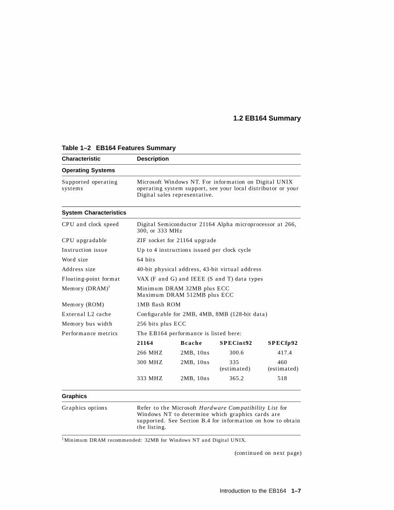
1.2 EB164 SummaryThe features of the EB164 are listed and described in Table 1–2.
1–6 Introduction to the EB164
1.2 EB164 Summary
Table 1–2 EB164 Features Summary
Characteristic Description
Operating Systems
Supported operatingsystems
Microsoft Windows NT. For information on Digital UNIXoperating system support, see your local distributor or yourDigital sales representative.
System Characteristics
CPU and clock speed Digital Semiconductor 21164 Alpha microprocessor at 266,300, or 333 MHz
CPU upgradable ZIF socket for 21164 upgrade
Instruction issue Up to 4 instructions issued per clock cycle
Word size 64 bits
Address size 40-bit physical address, 43-bit virtual address
Floating-point format VAX (F and G) and IEEE (S and T) data types
Memory (DRAM)1 Minimum DRAM 32MB plus ECCMaximum DRAM 512MB plus ECC
Memory (ROM) 1MB flash ROM
External L2 cache Configurable for 2MB, 4MB, 8MB (128-bit data)
Memory bus width 256 bits plus ECC
Performance metrics The EB164 performance is listed here:
21164 Bcache SPECint92 SPECfp92
266 MHZ 2MB, 10ns 300.6 417.4
300 MHZ 2MB, 10ns 335(estimated)
460(estimated)
333 MHZ 2MB, 10ns 365.2 518
Graphics
Graphics options Refer to the Microsoft Hardware Compatibility List forWindows NT to determine which graphics cards aresupported. See Section B.4 for information on how to obtainthe listing.
1Minimum DRAM recommended: 32MB for Windows NT and Digital UNIX.
(continued on next page)
Introduction to the EB164 1–7

1.2 EB164 Summary
Table 1–2 (Cont.) EB164 Features Summary
Characteristic Description
Input/Output
Input device interfaces PS/2 style keyboard and mouse
Serial Two RS423-compatible (9-position) serial communicationsports
Parallel One parallel (Centronics compatible) communications port
Bus options Total of 6 option slots
PCI bus Supports two 64-bit PCI options slots at 5V and two 32-bitPCI option slots at 5V
ISA bus Supports three 16-bit ISA option slots
IDE One IDE interface supporting up to 2 drives
Diskette One 82077-compatible diskette controller supporting up to 2drives with 1.44MB and 2.88MB formats
Environmental Characteristics (Operating)
Operating temperature 10°C to 40°C (50°F to 104°F)
Maximum rate of (drybulb) temperaturechange
11°C/hour �2°C/hour (20°F/hour �4°F/hour)
Relative humidityMaximum wet bulbMinimum dew point
10%–90% noncondensing32°C (90°F)2°C (36°F)
EMC compliance Compliance certification is the responsibility of the systemintegrator. The EB164 was tested in industry-representativeenclosures to prove feasibility of emissions compliance.
Shock and vibration Passing of shock and vibration tests is dependent on themethod used to mount the system board, the design of theenclosure, and how the enclosure is supported. Testing isthe responsibility of the system integrator.
Physical Characteristics
Form factor Standard, full-size PC AT board
Width/depth 30.73 cm (12.10 in) � 33.15 cm (13.05 in)
1–8 Introduction to the EB164

2System Configuration and Connectors
The EB164 uses jumpers to implement configuration parameters suchas variations in backup cache (Bcache) size, access timing, and speed, aswell as boot parameters. These jumpers must be configured for the user’senvironment. Onboard connectors are provided for the I/O interfaces, singleinline memory modules (SIMMs), and serial and parallel peripheral ports.
After the module is configured, power can be applied, and the debug monitorcan be run. The debug monitor and its commands are described in the AlphaMicroprocessors Evaluation Board Debug Monitor User’s Guide. Appendix Bprovides information about other software design tools.
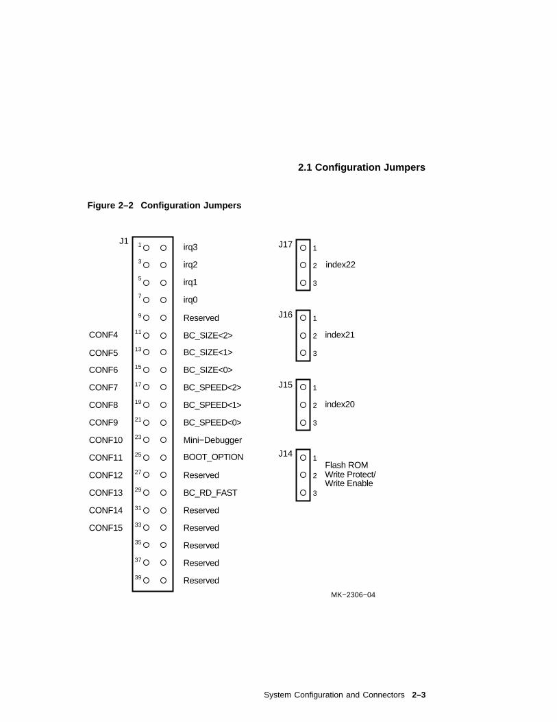
2.1 Configuration JumpersFigure 2–1 identifies the location of the software and hardware configurationjumpers, and Table 2–1 provides descriptions. Figure 2–2 provides a detailedview of the configuration jumpers and their function.
System Configuration and Connectors 2–1

2.1 Configuration Jumpers
Figure 2–1 EB164 Jumper Locations
MK−2306−30
11
J1
1
J14
J17
J16
J15
1
2–2 System Configuration and Connectors
2.1 Configuration Jumpers
Figure 2–2 Configuration Jumpers
J1irq3 1
2
3
index22
index21
index20
J17
J16
J15
MK−2306−04
BC_SIZE<2>
BC_SIZE<1>
BC_SIZE<0>
BC_SPEED<2>
BC_SPEED<1>
BC_SPEED<0>
Mini−Debugger
BOOT_OPTION
BC_RD_FAST
Reserved
Reserved
irq0
irq1
irq2
Reserved
Reserved
1
3
5
7
9
11
13
15
17
19
21
23
25
27
29
31
33
35
37
39
J14Flash ROM
1
2
3
1
2
3
1
2
3
Write Protect/Write Enable
Reserved
Reserved
CONF4
CONF5
CONF6
CONF7
CONF8
CONF9
CONF10
CONF11
CONF12
CONF13
CONF14
CONF15
Reserved
System Configuration and Connectors 2–3

2.1 Configuration Jumpers
Table 2–1 Configuration Jumper Position Descriptions
Feature Jack/Jumper—Pins and Description
System clockdivisor
J1—1/2, —3/4, —5/6, —7/8
J1—1/2(irq3)
J1—3/4(irq2)
J1—5/6(irq1)
J1—7/8(irq0) Ratio
In In Out Out 3
In Out In In 4
In Out In Out 5
In Out Out In 6
In Out Out Out 7
Out In In In 8
Divisor 8 is used for 266 MHz.
Out In In Out 9
Divisor 9 is used for 300 MHz.
Out In Out In 10
Divisor 10 is used for 333 MHz.
Out In Out Out 11
Out Out In In 12
Out Out In Out 13
Out Out Out In 14
Out Out Out Out 15
(continued on next page)
2–4 System Configuration and Connectors

2.1 Configuration Jumpers
Table 2–1 (Cont.) Configuration Jumper Position Descriptions
Feature Jack/Jumper—Pins and Description
BC_SIZE<2:0> J1—11/12 (CONF4), —13/14 (CONF5), —15/16 (CONF6)
These jumpers allow the Bcache to emulate the sizes specifiedin the following table. These jumpers are changed in conjunctionwith the appropriate index jumpers J17, J16, and J15.
CONF4Pins 11/12
CONF5Pins 13/14
CONF6Pins 15/16 Bcache
In In In Reserved
In In Out Reserved
In Out In Reserved
In Out Out 2MB (default)
Out In In 4MB
Out In Out 8MB
Out Out In Reserved
Out Out Out Reserved
Bcache size–index address bits<22:20>
J17, J16, J15
Jumper2MB1
(default) 4MB 2 8MB2
J17 (index22) 2 to 3 2 to 3 1 to 2
J16 (index21) 2 to 3 1 to 2 1 to 2
J15 (index20) 1 to 2 1 to 2 1 to 2
1SIMMs populated with 128K � 8 or 512K � 8 SRAMs2SIMMs populated with 512K � 8 SRAMs
(continued on next page)
System Configuration and Connectors 2–5

2.1 Configuration Jumpers
Table 2–1 (Cont.) Configuration Jumper Position Descriptions
Feature Jack/Jumper—Pins and Description
BC_SPEED<2:0> J1—17/18 (CONF7), —19/20 (CONF8), —21/22 (CONF9)
These jumpers select the Bcache timing parameters used tocompute the BC_CONFIG register value. Select the jumperconfiguration that matches the access time for the SRAMs beingused.
CONF7Pins17/18
CONF8Pins19/20
CONF9Pins21/22 Bcache Speed
In In In Reserved
In In Out 6-ns SRAM timing
In Out In 8-ns SRAM timing
In Out Out 10-ns SRAM timing (default)
Out In In 12-ns SRAM timing
Out In Out 15-ns SRAM timing
Out Out In Reserved
Out Out Out Reserved
Mini-Debugger J1—23/24 (CONF10)
The Alpha SROM Mini-Debugger is provided in the SROM. Thisjumper (In) causes the SROM initialization to trap to the Mini-Debugger (connector J13) after all initialization is complete, butbefore starting the execution of the system flash ROM code. Thedefault position for this jumper is out.
(continued on next page)
2–6 System Configuration and Connectors

2.1 Configuration Jumpers
Table 2–1 (Cont.) Configuration Jumper Position Descriptions
Feature Jack/Jumper—Pins and Description
BOOT_OPTION J1—25/26 (CONF11)
This jumper selects the image to be loaded into memory fromthe system flash ROM. With the jumper out (bit = 1), the firstimage (debug monitor) is loaded. With the jumper in (bit = 0),alternate images can be loaded depending upon the value stored inTOY RAM location 0x3F. The default position for this jumper is in.
For system flash ROMs that contain a single image, the header isoptional. If the header does not exist, the entire 1MB system flashROM is loaded and executed at physical address zero.
For more information on the system ROM header and boot images,refer to Section 4.5.1.
BC_RD_FAST J1—29/30 (CONF13)
This jumper forces a Bcache read speed setting of 1 cycle fasterthan nominal.
BC_RD_FAST Bcache Speed
In Make read speed 1 cycle faster
Out Nominal read speed (default)
Flash ROM write-protect/write-enable jumper
J14
Jumper Pins Function
1 to 2 Flash ROM write-protect
2 to 3 Flash ROM write-enable (default)
System Configuration and Connectors 2–7

2.2 EB164 Connectors
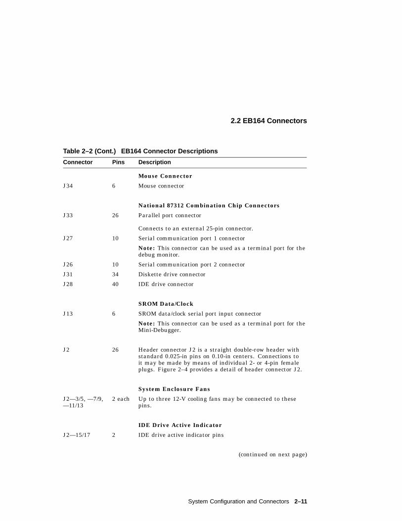
2.2 EB164 ConnectorsFigure 2–3 shows the EB164 connectors and Table 2–2 describes them.Figure 2–4 provides a detail of header connector J2.
Figure 2–3 EB164 Connector Locations
J10
J9
MK−2306−31
J7
J8
J25
J24
J30
J20
J19
J21
J6
J5
J3
J4
J28
J13
J23
J22
11
J29J18
J27
J26
J31
J33
J2
1
J11
J12
1
J34
J32
2–8 System Configuration and Connectors

2.2 EB164 Connectors
Figure 2–4 Detail of Header Connector J2
J2 Ground Pins:
MK−2306−27A
1
3
5
7
9
11
13
15
17
19
21
23
25
5, 8, 9, 12, 13, 16,18, 22, and 25
+12−V Pins:3, 7, and 11
Fan 1
Fan 2
Fan 3
IDE DriveActive
Power On
System Halt Button
System Reset Button
Keyboard Lock SwitchIndicator
Indicator
Speaker
System Configuration and Connectors 2–9

2.2 EB164 Connectors
Table 2–2 EB164 Connector Descriptions
Connector Pins Description
Main Memory/Bcache SIMMs
J10 72 DRAM 0 SIMM
J9 72 DRAM 1 SIMM
J8 72 DRAM 2 SIMM
J7 72 DRAM 3 SIMM
J6 72 DRAM 4 SIMM
J5 72 DRAM 5 SIMM
J4 72 DRAM 6 SIMM
J3 72 DRAM 7 SIMM
Note: To fill a 256-bit data path, all SIMM connectors J3through J10 must be populated.
J11 60 Bcache 0 SIMM
J12 60 Bcache 1 SIMM
Note: Both Bcache SIMM connectors must be populated.
PCI Connectors
J22 184 PCI64 connector 0
J23 184 PCI64 connector 1
J24 124 PCI32 connector 2
J25 124 PCI32 connector 3
ISA Connectors
J19 98 ISA connector slot 0
J20 98 ISA connector slot 1
J21 98 ISA connector slot 2
Keyboard Connector
J32 6 Keyboard connector
(continued on next page)
2–10 System Configuration and Connectors
2.2 EB164 Connectors
Table 2–2 (Cont.) EB164 Connector Descriptions
Connector Pins Description
Mouse Connector
J34 6 Mouse connector
National 87312 Combination Chip Connectors
J33 26 Parallel port connector
Connects to an external 25-pin connector.
J27 10 Serial communication port 1 connector
Note: This connector can be used as a terminal port for thedebug monitor.
J26 10 Serial communication port 2 connector
J31 34 Diskette drive connector
J28 40 IDE drive connector
SROM Data/Clock
J13 6 SROM data/clock serial port input connector
Note: This connector can be used as a terminal port for theMini-Debugger.
J2 26 Header connector J2 is a straight double-row header withstandard 0.025-in pins on 0.10-in centers. Connections toit may be made by means of individual 2- or 4-pin femaleplugs. Figure 2–4 provides a detail of header connector J2.
System Enclosure Fans
J2—3/5, —7/9,—11/13
2 each Up to three 12-V cooling fans may be connected to thesepins.
IDE Drive Active Indicator
J2—15/17 2 IDE drive active indicator pins
(continued on next page)
System Configuration and Connectors 2–11

2.2 EB164 Connectors
Table 2–2 (Cont.) EB164 Connector Descriptions
Connector Pins Description
Speaker
J2—19/21/23/25 — Speaker connector pins
Power On Indicator
J2—26 1 Power on indicator pin
Connect LED from this pin to ground.
System Halt Button
J2—8/10 2 System halt button pins
System Reset Button
J2–12/14 2 System reset button pins
Keyboard Lock Switch
J2–18/20 2 Keyboard lock switch pins
(continued on next page)
2–12 System Configuration and Connectors

2.2 EB164 Connectors
Table 2–2 (Cont.) EB164 Connector Descriptions
Connector Pins Description
Power Connectors
J18 12 Board power connector
Pin Voltage/Signal
1 +3.3 V
2 +3.3 V
3 +3.3 V
4 Ground
5 Ground
6 Ground
7 Ground
8 Ground
9 Ground
10 +3.3 V
11 +3.3 V
12 +3.3 V
(continued on next page)
System Configuration and Connectors 2–13

2.2 EB164 Connectors
Table 2–2 (Cont.) EB164 Connector Descriptions
Connector Pins Description
J29 12 Board power connector
Pin Voltage/Signal
1 p_dcok
2 Vdd (+5 V)
3 +12 V
4 –12 V
5 Ground
6 Ground
7 Ground
8 Ground
9 –5 V
10 Vdd (+5 V)
11 Vdd (+5 V)
12 Vdd (+5 V)
Note: Power for the EB164 is provided by a user-suppliedpower supply. Digital does not provide this power supply.(Refer to Chapter 5 for more information.)
J30 3 CPU fan power and sensor
Caution: Fan sensor required.
The fan must have a built-in sensor that drives a signalif the airflow stops. The sensor must be connected to pinJ30—2. The fan supplied with the EB164 includes an airflowsensor.
2–14 System Configuration and Connectors

3Starting and Using the EB164
This chapter lists hardware, software, and accessories that users must obtainto completely furnish a functioning computer system. The chapter thendescribes how to configure the hardware and software. Finally, the chapterdescribes how to start and use the EB164.
3.1 Hardware RequirementsBefore turning on the power to your EB164, you must provide the followingcomponents in addition to those supplied in the kit. The components neededdepend upon the intended use of the EB164 board.
• A 21164 Alpha microprocessor (266-, 300-, or 333-MHz speed).
• If a 300-MHz or 333-MHz microprocessor is used, the oscillator must bechanged. Refer to Appendix A for part numbers and sources. The boardships with parts to complement a 266-MHz microprocessor.
• Eight 72-pin, 36-bit, 5-V, DRAM SIMM memory modules (connectorsJ3 through J10). SIMMs must consist of identical devices. Digitalrecommends that all SIMMs be purchased from the same vendor.
• Two Alpha L3 cache SRAM SIMMs (connectors J11 and J12). Partnumbers for 2MB cache sizes are listed in Appendix A.
• An industry-standard PC power supply that includes a 3.3-V dc output,rated at a minimum of 339 W (refer to Appendix A).
• A PS/2 compatible 101-key keyboard.
• A PS/2 compatible mouse.
• A supported PCI or ISA bus graphics card, cables, and a compatiblemonitor.
• A supported PCI or ISA bus SCSI controller and cables.
• A SCSI CD–ROM drive.
• An IDE or SCSI hard drive.
Starting and Using the EB164 3–1

3.1 Hardware Requirements
• A 3.5-in diskette drive and cable.
• A 9-pin serial line cable.
• A terminal or a serial line connection to a host system with appropriatecables.
Refer to the Alpha Microprocessors Evaluation Board Windows NT 3.51Installation Guide provided in the EB164 Windows NT 3.51 Installation Kitand the Hardware Compatibility List for Windows NT to determine whichSCSI controllers and graphics cards are supported.
For more information about hardware requirements and for the location ofboard connectors and jumpers, see Chapter 2.
3.2 Software RequirementsThe following software media is required to install and run the Windows NToperating system:
• A Windows NT 3.51 CD–ROM
• An EB164 Windows NT 3.51 installation diskette
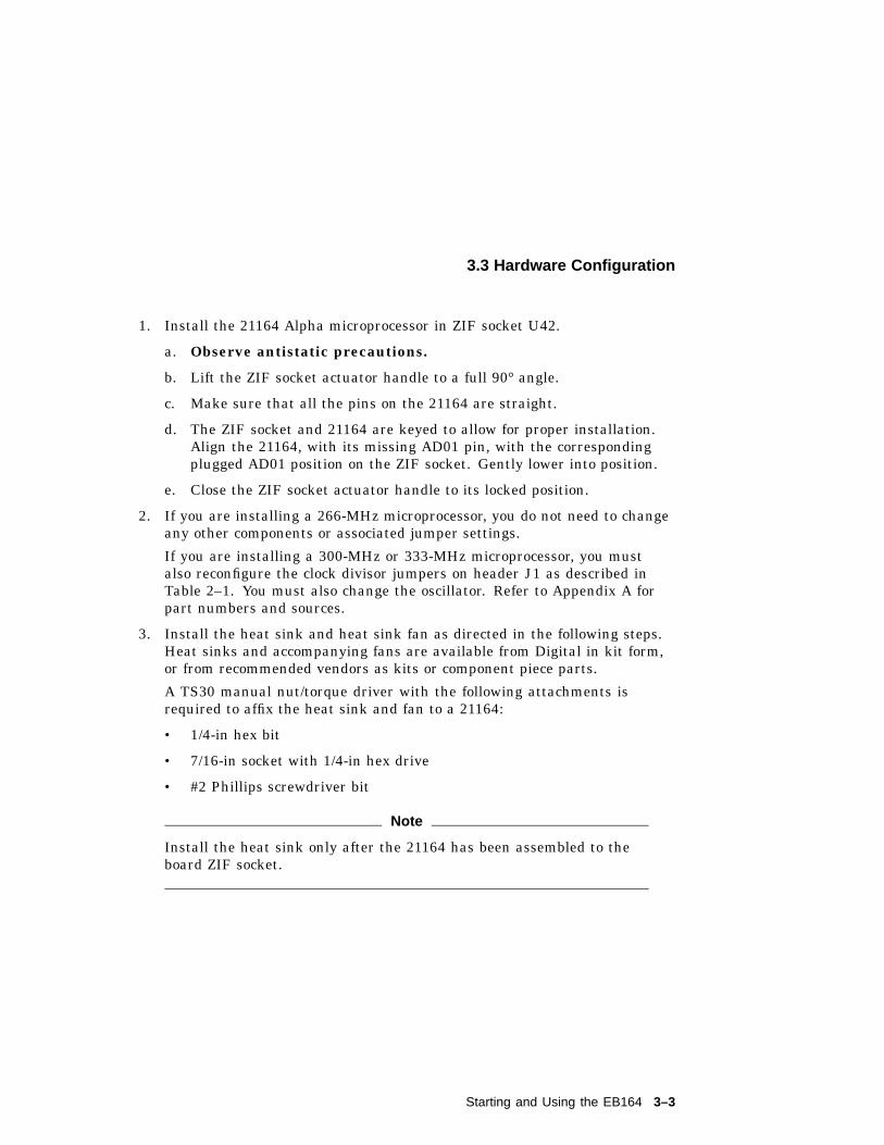
3.3 Hardware ConfigurationOnce you have acquired the necessary hardware, it must be assembled intoa system. This section lists the necessary steps. The system does not haveto be assembled in the order presented. However, if you are installing themotherboard into an enclosure, Digital recommends that you install themicroprocessor and heat sink first.
Caution: Static-Sensitive Component
Due to the sensitive nature of electronic components to static electricity,Digital strongly advises that anyone handling the 21164 Alphamicroprocessor wear a properly grounded antistatic wrist strap. Useof antistatic mats, ESD approved workstation, or exercising other goodESD practices is recommended.
3–2 Starting and Using the EB164
3.3 Hardware Configuration
1. Install the 21164 Alpha microprocessor in ZIF socket U42.
a. Observe antistatic precautions.
b. Lift the ZIF socket actuator handle to a full 90° angle.
c. Make sure that all the pins on the 21164 are straight.
d. The ZIF socket and 21164 are keyed to allow for proper installation.Align the 21164, with its missing AD01 pin, with the correspondingplugged AD01 position on the ZIF socket. Gently lower into position.
e. Close the ZIF socket actuator handle to its locked position.
2. If you are installing a 266-MHz microprocessor, you do not need to changeany other components or associated jumper settings.
If you are installing a 300-MHz or 333-MHz microprocessor, you mustalso reconfigure the clock divisor jumpers on header J1 as described inTable 2–1. You must also change the oscillator. Refer to Appendix A forpart numbers and sources.
3. Install the heat sink and heat sink fan as directed in the following steps.Heat sinks and accompanying fans are available from Digital in kit form,or from recommended vendors as kits or component piece parts.
A TS30 manual nut/torque driver with the following attachments isrequired to affix the heat sink and fan to a 21164:
• 1/4-in hex bit
• 7/16-in socket with 1/4-in hex drive
• #2 Phillips screwdriver bit
Note
Install the heat sink only after the 21164 has been assembled to theboard ZIF socket.
Starting and Using the EB164 3–3

3.3 Hardware Configuration
Refer to Figure 3–1 for heat sink and fan assembly details.
Figure 3–1 Fan/Heat Sink Assembly
21164 Alpha Microprocessor
LJ04412A.AI5
Heat Sink, with Fan Mounting Holes
Nut, Hex, 1/4-20, 2011-T3 Aluminum, 0.438 in Across Flats, Qty 2 Torque to 20 +/- 2 in-lbs
Clip, Heat Sink/Chip/Fan
Thermal Pad
Guard, Fan
Screw, 6-32 x 0.875 in Qty 4
Fan
a. Put the GRAFOIL thermal pad in place. The GRAFOIL pad is usedto improve the thermal conductivity between the chip package and theheat sink by replacing micro air pockets with a less insulative material.Perform the following steps to position the GRAFOIL pad:
1) Perform a visual inspection of the package slug to ensure that it isfree of contamination.
3–4 Starting and Using the EB164

3.3 Hardware Configuration
2) Wearing clean gloves, pick up the GRAFOIL pad. Do not do thiswith bare hands because skin oils can be transferred to the pad.
3) Place the GRAFOIL pad on the gold-plated slug surface and alignit with the threaded studs.
b. Attach the microprocessor heat sink. The heat sink material is clearanodized, hot-water-sealed, 6061-T6 aluminum. The nut material is2011-T3 aluminum (this grade is critical). Perform the following stepsto attach the heat sink:
1) Observe antistatic precautions.
2) Align the heat sink holes with the threaded studs on the ceramicpackage.
3) Handle the heat sink by the edges and lower it on to the chippackage, taking care not to damage the stud threads.
4) Set a calibrated torque driver to 20 in-lb, �2 in-lb, (2.3 N m,�0.2 N m.) The torque driver should have a mounted 7/16-insocket.
5) Insert a nut into the 7/16-in socket, place on one of the studs, andtighten to the specified torque. Repeat for second nut.
6) If the sink/chip/fan clip is used, install it properly by positioningit over the assembly and hooking its ends around the ZIF socketretainers.
c. Perform the following steps to attach the heat sink fan assembly:
1) Place the fan assembly on top of the heat sink, aligning the fanmounting holes with the corresponding threaded heat sink holes.Align the fan so that the fan power/sensor wires exit the fan closestto connector J30 (see Figure 2–3). Fan airflow must be directedinto the heat sink (fan label facing down toward the heat sink).
2) Place the fan guard on top of the fan. Orient the guard so that thecorner mounting areas lay flush against the heat sink.
3) Secure the fan and fan guard to the heat sink with four6–32 � 0.875-in screws.
4) Plug the fan power/sensor cable into connector J30 (seeFigure 2–3).
Starting and Using the EB164 3–5

3.3 Hardware Configuration
4. Install the two L3 cache SRAM SIMMs into sockets J11 and J12. Refer toTable 2–2 for socket locations.
5. Install eight system memory DRAM SIMMs. Refer to Table 2–2 for socketlocations.
a. Observe antistatic precautions. Handle SIMMs at the edges only toprevent damage.
b. SIMMs must be installed in groups of eight consisting of identicaldevices.
c. Hold the SIMM at an angle with the notch facing the key in the socket.
d. Firmly push the module into the connector and stand the moduleupright.
e. Make sure that the SIMM snaps into the metal locking clips on bothends.
6. If you intend to mount the motherboard in a system enclosure, do so now.Install the power supply into the enclosure first, then the motherboard.Appendix A lists a suggested enclosure and a suggested power supply. Theenclosure you use should be able to accept a standard, full-size PC ATboard.
7. Connect the power supply to the EB164 board, as shown in Figure 3–2,with standard power to J29, and with 3.3-V dc power to J18.
8. If you are using an enclosure, mount the 3.5-in diskette drive, hard drive,and CD–ROM drive. Refer to the manufacturer’s instructions for installingthese devices.
9. Connect the supplied 3.5-inch diskette drive. The 34-pin diskette drivecable goes from connector J31 on your EB164 to the diskette drive. Thedrive should be connected at the very end of the cable closest to the twistin the cable. Attach a power connector to the drive. Again, make sure toinsert the connector in the proper orientation so that pin 1 on the cablematches pin 1 on the board header (as indicated on the module).
10. Install the SCSI controller in a free PCI or ISA connector and attach theCD–ROM drive. If you will be using a SCSI hard drive, install the harddrive now. Refer to the manufacturer’s instructions for installing thesedevices. Verify that a unique SCSI ID is assigned to each device you attachto the SCSI bus.
3–6 Starting and Using the EB164

3.3 Hardware Configuration
Figure 3–2 EB164 Power Connectors
MK−2306−28
1
1
J29
J18
EB164 Board
21164
Microprocessor
J29Pin Voltage/Signal12 (+5 V)3 +12 V4 −12 V5 Ground6 Ground7 Ground8 Ground9 −5 V10 (+5 V)11 (+5 V)12 (+5 V)
Pin Voltage/Signal1 +3.3 V2 +3.3 V3 +3.3 V4 Ground5 Ground6 Ground7 Ground8 Ground9 Ground10 +3.3 V11 +3.3 V12 +3.3 V
J18
p_dcokVdd
VddVddVdd
Starting and Using the EB164 3–7

3.3 Hardware Configuration
11. If you will be using an IDE hard drive, attach your IDE cable to connectorJ28 in the proper orientation and install your hard drive. The diskshould be configured as the primary device on the IDE bus. Refer to themanufacturer’s instructions for setting up the hard drive.
12. If you plan to use your EB164 on a network, install the Ethernet controllerboard (DE435) in one of the PCI connectors as outlined in the DE435documentation.
13. Install the graphics card into either a PCI or ISA connector, depending onthe card you are using. Connect the graphics card to a compatible monitorfollowing the graphics card manufacturer’s instructions.
14. Connect the keyboard cable to connector J32.
15. Connect the mouse cable to connector J34.
16. Connect the 9-pin serial port adapter cable, provided in the kit, to theCOM1 connector at J27. Insert the connector in the proper orientation, sothat pin 1 on the cable matches pin 1 on the board header (as indicated onthe module).
17. Connect your terminal to the COM1 port, using a cable arrangementappropriate to your terminal. Set the terminal to 9600 baud, 8 data bits, 1stop bit, no parity.
18. Connect miscellaneous items such as, enclosure fans, reset button, speaker,power indicator, hard drive active indicator (if using an IDE drive),keyboard lock switch, and so forth.
3.4 Software ConfigurationTwo firmware programs have been loaded into the EB164 1MB flash ROM.They are the debug monitor and the Windows NT ARC firmware. The debugmonitor is a serial line monitor program used to perform software andhardware debug functions. The Windows NT ARC firmware is used to load andboot Windows NT. The EB164 system has been configured to start the WindowsNT ARC firmware by default.
The serial ROM firmware uses a value stored in the nonvolatile RAM of thereal-time clock to determine which firmware image to load. Once the WindowsNT ARC firmware is running, you can switch to the debug monitor firmware.
3–8 Starting and Using the EB164

3.4 Software Configuration
3.4.1 Starting Windows NT ARC FirmwareStart the Windows NT ARC firmware using the following procedure.
1. Verify that the jumper from J14-2 to J14-3 is inserted, allowing the flashROM to be written. If the Windows NT ARC firmware is unable to write toflash ROM, it prints the device error message and stops.
2. Verify that the jumper at J1–25/26 is installed (see CONF11 on themodule). The presence of the jumper at J1–25/26 forces the serialROM firmware to load the alternate image selected by the value in thenonvolatile TOY RAM. The absence of this jumper overrides the valuestored in the TOY RAM and causes the first image, the debug monitor, tobe loaded.
3. Turn on the power to the EB164. After the power-up diagnostics are run,the ARC console boot menu appears on the graphics display.
If the ARC console boot menu does not appear, check the output of COM1for error messages and review your hardware configuration.
You are ready for software installation. Refer to the Alpha MicroprocessorsEvaluation Board Windows NT 3.51 Installation Guide for instructions.
3.4.2 Going to the Debug Monitor from Windows NT ARC FirmwareYou may use either of these two methods to access the debug monitor from theWindows NT ARC firmware.
A. Use the ARC firmware menus to choose the debug monitor.
1. At the Boot menu, choose Supplementary menu....
2. At the Supplementary menu, choose Setup the system....
3. At the Setup the system menu, choose Machine specific setup....
4. At the Machine specific setup menu, choose Debug Monitor.
5. Turn off the power to the EB164, then turn the power back on.
B. Turn off the power to the EB164, remove the jumper from J1-25/26(CONF11 on the module), then turn on the power to the EB164.
Starting and Using the EB164 3–9

3.4 Software Configuration
3.4.3 Returning to Windows NT ARC Firmware from the Debug MonitorThe following methods may be used to return to the Windows NT ARCfirmware from the debug monitor.
A. If you used item A in section Section 3.4.2 to enter the debug monitor, thenuse this procedure to return to Windows NT ARC firmware.The firmware contained in the serial ROM on your EB164 determineswhich firmware image is loaded from the flash ROM at power-up. Theserial ROM firmware uses a value stored in the nonvolatile RAM of thereal-time clock to determine which firmware image to load. At this point,you want the serial ROM to load the Windows NT ARC firmware.
1. Use the following debug monitor commands to select Windows NT ARCfirmware, by writing the value 1 to the TOY RAM. and to verify theselection:
EB164> bootopt nt
O/S type selected: "The Windows NT Operating System"....Firmware type: "Windows NT Firmware"
EB164> bootopt
Predefined bootoptions are..."0" "Alpha Evaluation Board Debug Monitor" "DBM""1" "The Windows NT Operating System" "NT""2" "OpenVMS" "VMS""3" "Digital UNIX" "UNIX"
O/S type selected: "The Windows NT Operating System"....Firmware type: "Windows NT Firmware"
EB164>
Note
The EB164 does not support the OpenVMS operating system.
2. Turn off power to the EB164. Verify the presence of a jumper atJ1–25/26 (see CONF11 on the module).
3. Turn on the power to the EB164. After the power-up diagnostics arerun, the ARC console boot menu appears on the graphics display.
3–10 Starting and Using the EB164

3.4 Software Configuration
B. If you used item B in section Section 3.4.2 to enter the debug monitor, thenuse this procedure to return to Windows NT ARC firmware.
1. Turn off the power to the EB164, insert the jumper from J1-25/26(CONF11 on the module).
2. Turn on the power to the EB164. After the power-up diagnostics arerun, the ARC console boot menu appears on the graphics display.If the ARC console boot menu does not appear, check the output ofCOM1 for error messages and review your hardware configuration.
Starting and Using the EB164 3–11


4Functional Description
This chapter describes the functional operation of the EB164. The descriptionintroduces the Digital Semiconductor 21171 ASIC support chipset anddescribes its implementation with the 21164 microprocessor, its supportingmemory, and I/O devices. Figure 1–1 shows the EB164 major functionalcomponents.
Information, such as bus timing and protocol, found in other data sheetsand reference documentation is not duplicated. See Appendix B for a list ofsupporting documents and order numbers.
Note
For detailed descriptions of bus transactions, chipset logic, andoperation, refer to the Alpha 21164 Microprocessor Hardware ReferenceManual and the DECchip 21171 Core Logic Chipset Technical ReferenceManual.
For details of the PCI interface, refer to the PCI System Design Guide.
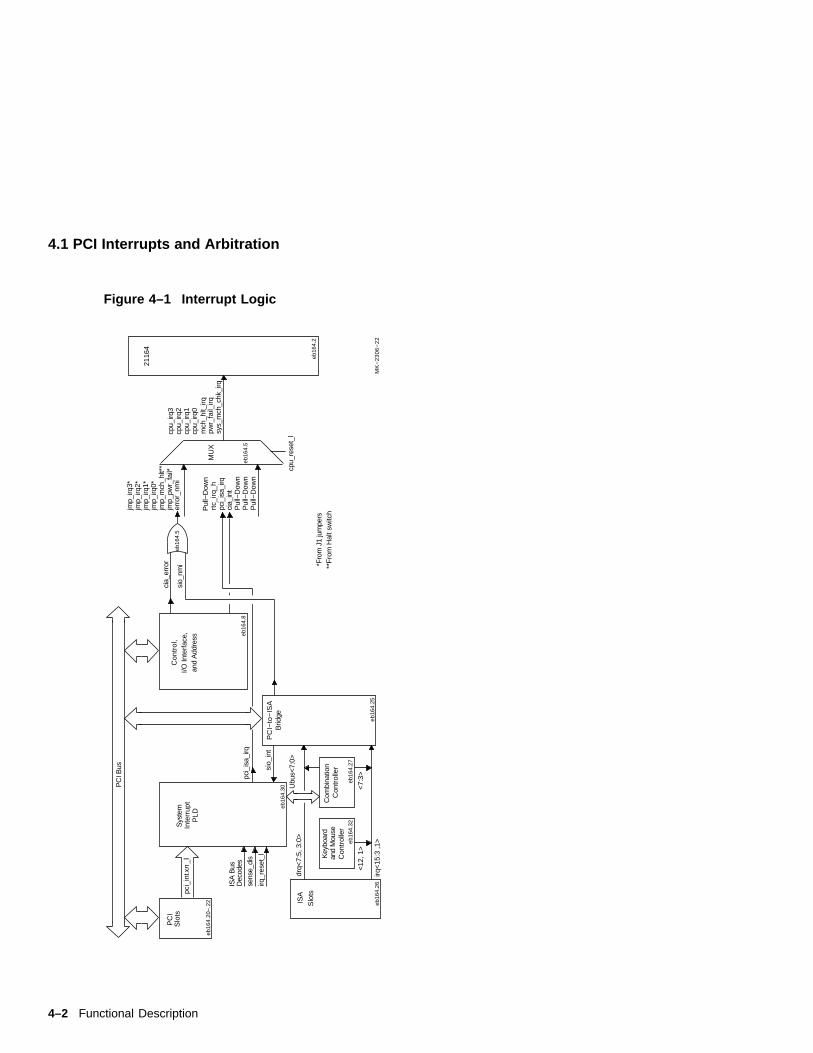
4.1 PCI Interrupts and ArbitrationThe following sections describe the EB164 interrupt and arbitration (arbiter)logic.
4.1.1 InterruptsPCI-, ISA-, and CIA-generated interrupts are each described. Figure 4–1 showsthe interrupt logic.
Functional Description 4–1
4.1 PCI Interrupts and Arbitration
Figure 4–1 Interrupt Logic
PC
I Bus
2116
4
eb16
4.2
cpu_
rese
t_l
Key
boar
dan
d M
ouse
Con
trol
ler
ISA
PC
I−to
−IS
AB
ridge
Com
bina
tion
Con
trol
ler
irq<
15:3
,1>
<7:3
><1
2, 1
>
drq<
7:5,
3:0
>
eb16
4.25
eb16
4.27
eb16
4.32
PC
IS
lots
MK
−2
30
6−
22
Sys
tem
Inte
rrup
tP
LD
eb16
4.30
sio_
int
eb16
4.20
−.2
2 eb16
4.26
MU
X
eb16
4.5
Slo
ts
sys_
mch
_chk
_irq
jmp_
irq3*
Con
trol
,
and
Add
ress
eb16
4.8
pci_
int
_l
xn
Ubu
s<7:
0>
cia_
erro
r
sio_
nmi
jmp_
irq2*
jmp_
irq1*
jmp_
irq0*
jmp_
pwr_
fail*
jmp_
mch
_hlt*
*
erro
r_nm
i
Pul
l−D
own
rtc_
irq_h
pci_
isa_
irqci
a_in
tP
ull−
Dow
nP
ull−
Dow
n
cpu_
irq3
pwr_
fail_
irqm
ch_h
lt_irq
cpu_
irq0
cpu_
irq1
cpu_
irq2
irq_r
eset
_l
Dec
odes
sens
e_di
s
ISA
Bus
pci_
isa_
irq
eb16
4.5
I/O In
terf
ace,
Pul
l−D
own
*Fro
m J
1 ju
mpe
rs**
Fro
m H
alt s
witc
h
4–2 Functional Description
4.1 PCI Interrupts and Arbitration
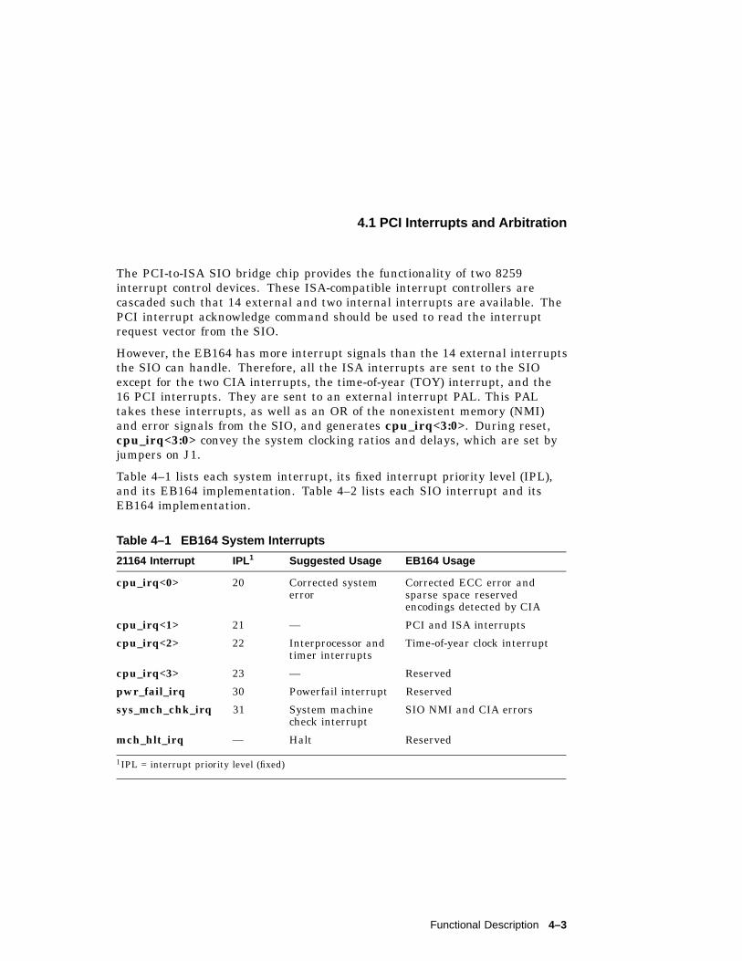
The PCI-to-ISA SIO bridge chip provides the functionality of two 8259interrupt control devices. These ISA-compatible interrupt controllers arecascaded such that 14 external and two internal interrupts are available. ThePCI interrupt acknowledge command should be used to read the interruptrequest vector from the SIO.
However, the EB164 has more interrupt signals than the 14 external interruptsthe SIO can handle. Therefore, all the ISA interrupts are sent to the SIOexcept for the two CIA interrupts, the time-of-year (TOY) interrupt, and the16 PCI interrupts. They are sent to an external interrupt PAL. This PALtakes these interrupts, as well as an OR of the nonexistent memory (NMI)and error signals from the SIO, and generates cpu_irq<3:0>. During reset,cpu_irq<3:0> convey the system clocking ratios and delays, which are set byjumpers on J1.
Table 4–1 lists each system interrupt, its fixed interrupt priority level (IPL),and its EB164 implementation. Table 4–2 lists each SIO interrupt and itsEB164 implementation.
Table 4–1 EB164 System Interrupts
21164 Interrupt IPL 1 Suggested Usage EB164 Usage
cpu_irq<0> 20 Corrected systemerror
Corrected ECC error andsparse space reservedencodings detected by CIA
cpu_irq<1> 21 — PCI and ISA interrupts
cpu_irq<2> 22 Interprocessor andtimer interrupts
Time-of-year clock interrupt
cpu_irq<3> 23 — Reserved
pwr_fail_irq 30 Powerfail interrupt Reserved
sys_mch_chk_irq 31 System machinecheck interrupt
SIO NMI and CIA errors
mch_hlt_irq — Halt Reserved
1IPL = interrupt priority level (fixed)
Functional Description 4–3

4.1 PCI Interrupts and Arbitration
Table 4–2 PCI-to-ISA SIO Bridge Interrupts
Priority Label Controller Internal/External Interrupt Source
1 IRQ0 1 Internal Internal timer 1
2 IRQ1 1 External Keyboard
3–10 IRQ2 1 Internal Interrupt from controller 2
3 IRQ8#1 2 External Reserved
4 IRQ9 2 External ISA bus pin B04
5 IRQ10 2 External ISA bus pin D03
6 IRQ11 2 External ISA bus pin D04
7 IRQ12 2 External Mouse
8 IRQ13 2 External Reserved
9 IRQ14 2 External IDE
10 IRQ15 2 External ISA bus pin D06
11 IRQ3 1 External 87312 combination controller
12 IRQ4 1 External 87312 combination controller
13 IRQ5 1 External 87312 combination controller
14 IRQ6 1 External 87312 combination controller
15 IRQ7 1 External 87312 combination controller
1The # symbol indicates an active low signal.
Interrupt PLDs FunctionThe MACH210A PLD is an 8-bit I/O slave on the ISA bus at hex addresses804, 805, and 806. This is accomplished by a decode of the three ISA addressbits sa<2:0> and the three ecas_addr<2:0> bits.
Each interrupt can be individually masked by setting the appropriate bit in themask register. An interrupt is disabled by writing a 1 to the desired positionin the mask register. An interrupt is enabled by writing a 0. For example,bit <7> set in interrupt mask register 1 indicates that the INTB2 interrupt isdisabled. There are three mask registers located at ISA addresses 804, 805,and 806.
An I/O read transaction at ISA addresses 804, 805, and 806 returns the state ofthe 17 PCI interrupts rather than the state of the masked interrupts. On readtransactions, a 1 means that the interrupt source shown in Figure 4–2 hasasserted its interrupt. The mask register can be updated by writing addresses804, 805, or 806. The mask register is write-only.
4–4 Functional Description

4.1 PCI Interrupts and Arbitration
Figure 4–2 Interrupt and Interrupt Mask Registers
RAZRAZRAZRAZRAZRAZRAZ intd3
7 6 5 4 3 2 1 0
LJ-04211.AI
Notes:
Interrupt and Interrupt Mask Register 3 (ISA Address 806h)
Interrupt and Interrupt Mask Register 2 (ISA Address 805h)
Interrupt and Interrupt Mask Register 1 (ISA Address 804h)
RAZ = Read-as-Zero, Read-OnlyInterrupt Mask Register Is Write-Only
intb3intc0intc1intc2intc3intd0intd1intd2
7 6 5 4 3 2 1 0
inta0inta1inta2inta3intb0intb1intb2 sio
7 6 5 4 3 2 1 0
4.1.2 ArbitrationArbitration logic is implemented in the Intel 82378ZB Saturn I/O (SIO)chip. The arbitration scheme is flexible and software programmable. Referto the Intel 82420/82430 PCIset ISA and EISA Bridges document for moreinformation about programmable arbitration.
4.2 ISA Bus DevicesTwo dedicated ISA expansion slots are provided in addition to the combinationISA/PCI slot. System support features such as serial lines, parallel port,integrated device electronics (IDE), and diskette controller are embedded onthe module by means of an 87312 combination controller chip. Also shown isthe utility bus (Ubus) with its system support devices.
4.3 dc Power DistributionThe EB164 derives its system power from a user-supplied PC power supply.The power supply must provide +12 V dc and –12 V dc, –5 V dc, +3 V dc,and Vdd (+5 V dc). The dc power is supplied through power connectors J18and J29. (See Figure 4–3.) Power is distributed to the board logic throughdedicated power planes within the 6-layer board structure.
Functional Description 4–5

4.3 dc Power Distribution
Figure 4–3 dc Power Distribution
ISA
Con
n.P
CI3
2 C
onn.
Pul
l−D
owns
+5 V
Pul
l−U
psIn
tegr
ated
Circ
uits
/Clo
cks
Spk
r
+3 V
Pul
l−U
ps
Fan
2116
4
eb16
4.2
MK
−2
30
6−
25
2 3 4 5 6J29
7 18 29 310 411 512 6J18
7 8 9 10 11 12
P/J
30
Vdd
+12
V−
12 V
−5
V
+3 V
GN
D (
Vss
)
eb16
4.22
eb16
4.26
Pow
erC
onne
ctor
seb
164.
40
Fan
s (J
1)Fl
ash
RO
M
4–6 Functional Description

4.3 dc Power Distribution
As shown in Figure 4–3, the +12 V dc, –12 V dc, and –5 V dc are supplied toISA connectors J19, J20, and J21. The +12 V dc and –12 V dc are suppliedto ISA connectors and PCI32 connectors J24 and J25. The +12 V dc is alsosupplied to the CPU fan connector J30, auxiliary fan connector pins on headerJ2, and to the flash ROM write-enable conector J14. Vdd is supplied to ISAconnectors, PCI32 connectors and most of the board’s integrated circuits. The+3 V dc is supplied to the 21164 microprocessor.
4.4 PCI DevicesThe EB164 uses the PCI bus as the main I/O bus for the majority of peripheralfunctions. The board implements the ISA bus as an expansion bus for systemsupport functions and relatively slow peripheral devices.
The PCI bus supports multiplexed, burst mode, read and write transfers.It supports synchronous operation of between 25 MHz and 33 MHz. It alsosupports either a 32-bit or 64-bit data path with 32-bit device support inthe 64-bit configuration. Depending upon the configuration and operatingfrequencies, the PCI bus supports anywhere between 100MB/s (25-MHz, 32-bit)to 264MB/s (33-MHz, 64-bit) peak throughput. The PCI provides parity onaddress and data cycles. Three physical address spaces are supported:
1. 32-bit memory space
2. 32-bit I/O space
3. 256-byte-per-agent configuration space
The bridge from the 21164 system bus to the 64-bit PCI bus is provided by theCIA chip. It generates the required 32-bit PCI address for 21164 I/O accessesdirected to the PCI. It also accepts 64-bit double address cycles and 32-bitsingle address cycles. However, the 64-bit address support is subject to someconstraints.
Functional Description 4–7

4.5 Flash ROM
4.5 Flash ROMThe flash ROM, sometimes called the system ROM, is a 1MB, nonvolatile,writable ROM. After the serial ROM (SROM) code initializes the EB164system, the flash ROM code prepares the system for booting. The flash ROMheaders, structure, and access methods are described here.
4.5.1 Special ROM HeaderThe MAKEROM tool is used to place a special header on ROM image files.The SROM allows the system (flash) ROM to contain several different ROMimages, each with its own header. The header informs the SROM where to loadthe image, and whether or not it has been compressed with the MAKEROMtool. The header is optional for system ROMs containing a single image. Ifthe header does not exist, the complete 1MB system flash ROM is loadedand executed starting at physical address zero. Figure 4–4 shows the headercontent.
Figure 4–4 Special Header Content
Validation Pattern 5A5AC3C3 0x00
31 0
MK−2306−19
Header Rev<7:0>Firmware ID<15:8>
Inverse Validation Pattern A5A53C3C
Header Size (Bytes)
Image Checksum
Image Size (Memory Footprint)
Decompression Flag
Destination Address Lower Longword
Destination Address Upper Longword
Reserved<31:16>
Flash ROM Image Size
Optional Firmware ID<31:0>
Optional Firmware ID<63:32>
Header Checksum (excluding this field)
0x04
0x08
0x0C
0x10
0x14
0x18
0x1C
0x24
0x2C
0x30
0x20
0x28
4–8 Functional Description

4.5 Flash ROM
Table 4–3 describes each entry in the special header.
Table 4–3 Special Header Entry Descriptions
Entry Description
Validation and inversevalidation pattern
This quadword contains a special signature pattern used tovalidate that the special ROM header has been located. Thepattern is 5A5AC3C3A5A53C3C.
Header size (bytes) This longword provides the size of the header block, whichvaries among versions of the header specification.
When the header is located, SROM code determines wherethe image begins based on the header size. Additional dataadded to the header is ignored by older SROM code.
A header size of 32 bytes implies version 0 of the headerspecifications.
Image checksum This longword is used to verify the integrity of the ROM.
Image size The image size is used by the SROM code to determine howmuch of the system flash ROM should be loaded.
Decompression flag The decompression flag informs the SROM code whetherthe MAKEROM tool was used to compress the ROM imagewith a repeating byte algorithm. The SROM code containsroutines that execute the decompression algorithm. Othercompression and decompression schemes, which workindependently from this scheme, may be employed.
Destination address This quadword contains the destination address for theimage. The SROM code loads the image at this address andbegins execution.
Firmware ID The firmware ID is a byte that specifies the firmware type.This information facilitates image boot options necessary toboot different operating systems.
Firmware NameFirmwareType Firmware Description
Debug monitor 0 Alpha evaluation boarddebug monitor
Windows NT 1 Windows NT ARC firmware
Alpha SRM 2 Alpha System ReferenceManual console
(continued on next page)
Functional Description 4–9

4.5 Flash ROM
Table 4–3 (Cont.) Special Header Entry Descriptions
Entry Description
Header revision The revision of the header specification used in this header.This is necessary to provide for changes to the headerspecification. Version 0 headers are identified by the size ofthe header (32 bytes).
Flash ROM image size The flash ROM image size reflects the size of the image asit is contained in the flash ROM.
Optional firmware ID This optional field can be used to provide additionalfirmware information such as firmware revision or acharacter descriptive string of up to 8 characters.
Header checksum The checksum of the header. This is used to validate thepresence of a header beyond the validation provided by thevalidation pattern.
4–10 Functional Description

4.5 Flash ROM
4.5.2 Flash ROM StructureDuring the power-up and initialization sequence, the EB164 always loads thefirst image if BOOT_OPTION=1 (jumper J1—25/26 not installed). Then thefirst image (the debug monitor) will be booted.
If jumper J1—25/26 (BOOT_OPTION) is installed (see Figure 2–2), the EB164reads the value at location 0x3F of the TOY RAM. The EB164 uses the valuefound there to determine which image will be selected (see Table 4–4). Theselected image is loaded and executed.
Table 4–4 Flash ROM Image Selection
TOY RAMValue1 Firmware ID 2 Image Description
0x00 0 Evaluation board debug monitor firmware
0x01 1 Windows NT ARC firmware
0x02 2 Alpha SRM firmware (OpenVMS)3
0x03 2 Alpha SRM firmware (Digital UNIX)3
0x8n NA4 SROM code loads the nth image from flash ROM.If n=0, the SROM code loads the entire flash ROMcontents.If n=1, 2, . . . , the SROM code loads the first image,second image, and so on.
1Operating system type. Found at TOY RAM address 0x3F.2Found in image header.3Note: SRM firmware is not included in the EB164 kit.The flash ROM contains only one of these images.4Not applicable.
If an image is specified and is not found, the EB164 loads the first image foundin the flash ROM with a valid header. If no valid header is found, the entire1MB flash image is loaded at address 0x00000000.
The following sequence of steps describes how to change the value stored inTOY RAM location 0x3F by using either the basic debug monitor commands orthe debug monitor bootopt command.
Functional Description 4–11

4.5 Flash ROM
Changing TOY RAM Location 0x3F—Debug Monitor bootopt CommandUse the debug monitor bootopt command to change the value in location 3F.In the example shown here, the bootopt command is used to change the valuein location 3F from 0 to 1:
EB164> bootopt !
Predefined bootoptions are..."0" "Alpha Evaluation Board Debug Monitor" "DBM""1" "The Windows NT Operating System" "NT""2" "OpenVMS" "VMS""3" "Digital UNIX" "UNIX"
O/S type selected: "Alpha Evaluation Board Debug Monitor"....Firmware type: "DBM Firmware"
EB164> bootopt nt "
O/S type selected: "The Windows NT Operating System"....Firmware type: "Windows NT Firmware"
EB164> bootopt #
Predefined bootoptions are..."0" "Alpha Evaluation Board Debug Monitor" "DBM""1" "The Windows NT Operating System" "NT""2" "OpenVMS" "VMS""3" "Digital UNIX" "UNIX"
O/S type selected: "The Windows NT Operating System"....Firmware type: "Windows NT Firmware"
EB164>
! Use the debug monitor bootopt command to see the image choices and notewhich image is selected.
" Use the debug monitor bootopt nt command to change the selected imagefrom 0 to 1.
# Use the debug monitor bootopt command to verify that the selected imagehas changed from 0 to 1.
4–12 Functional Description

4.5 Flash ROM
4.5.3 Flash ROM AccessThe flash ROM can be viewed as two banks of 512KB each. At power-upthe lower 512KB bank is accessed using the address range 86.FFF8.0000 to86.FFFF.FFFF.
Setting address bit 19 (flash_adr19) allows you to access the higher 512KBof flash ROM. Write a 1 to the register at address 0x800 to set address bit 19.Manually deposit a 1 to address 0x800 or enter the following command fromthe debug monitor:
> wb 800 1
The address range for the higher bank is 86.FFF8.0000 to 86.FFFF.FFFF, thesame as for the lower bank. Access is now to the higher bank and will continueuntil the EB164 is reset, or a 0 is written to the register at address 0x800.
Note
The write-enable jumper must be installed at J14—2/3 (see Figure 2–1and Figure 2–2). This enables writing to the flash ROM.
Functional Description 4–13


5EB164 Requirements, Power, and
Parameters
This chapter describes the EB164 environmental requirements, power, andphysical board parameters.
5.1 Power RequirementsThe EB164 derives its main dc power from a user-supplied power supply. Theboard has a total power dissipation of 116 W, excluding any plug-in PCI andISA devices. Table 5–1 lists the power requirement for each dc supply voltage.
The power supply must supply a dcok signal to the system reset logic.
Table 5–1 Power Supply dc Current Requirements
Voltage Current 1
+3.3 V dc 16.0 A
+5 V dc 10.0 A
–5 V dc 0 A
+12 V dc 1.0 A
–12 V dc 100.0 mA
1Values indicated are for a fully populated EB164 system module excluding plug-in PCI and ISAdevices, with a CPU clock speed of 266 MHz.
Caution: Fan Sensor Required
The 21164 cooling fan must have a built-in sensor that will drive asignal if the airflow stops. The sensor is connected to EB164 boardconnector J30. When the signal is generated, it resets the system.
EB164 Requirements, Power, and Parameters 5–1

5.2 Environmental Requirements
5.2 Environmental RequirementsThe 21164 microprocessor is cooled by a small fan blowing directly into thechip’s heat sink. The EB164 motherboard is designed to run efficiently usingonly this fan. Additional fans may be necessary depending upon cabinetry andI/O board requirements.
The EB164 is specified to run within the following environment:
Parameter Specification
Operating temperature 10°C to 40°C (50°F to 104°F)
Storage temperature –55°C to 125°C (–67°F to 257°F)
Relative humidity 10% to 90% with maximum wet bulb temperature 28°C(82°F) and minimum dew point 2°C (36°F)
Rate of (dry bulb)temperature change
11°C/hour �2°C/hour (20°F/hour �4°F/hour)
5.3 Physical Board ParametersThe EB164 board consists of a 6-layer printed-wiring board (PWB) withcomponents mounted to side 1 only. The board is populated with integratedcircuit packages together with supporting active and passive components. TheEB164 is a standard, full-size PC AT board with the following dimensions:
• Width: 30.73 cm (12.10 in ±0.0005 in)
• Length: 33.15 cm (13.05 in ±0.0005 in)
• Height: 6.0 cm (2.375 in)
The board can be used in certain desktop and deskside systems that haveadequate clearance for the 21164 heat sink and fan. All ISA and PCIexpansion slots are usable in standard desktop or deskside enclosures.
Figure 5–1 shows the board and component outlines, and identifies the majorcomponents. Table 5–2 lists the components. Refer to Chapter 2 for jumperand connector functions and locations.
5–2 EB164 Requirements, Power, and Parameters

5.3 Physical Board Parameters
Figure 5–1 Board Component Layout
MK−2306−32
11
1
1
2
3 4 5 6
7
8
9
10
11
12
13
14
15
16
17
18
19
20
21
1
(13.05 in)33.15 cm
(12.10 in)30.73 cm
EB164 Requirements, Power, and Parameters 5–3
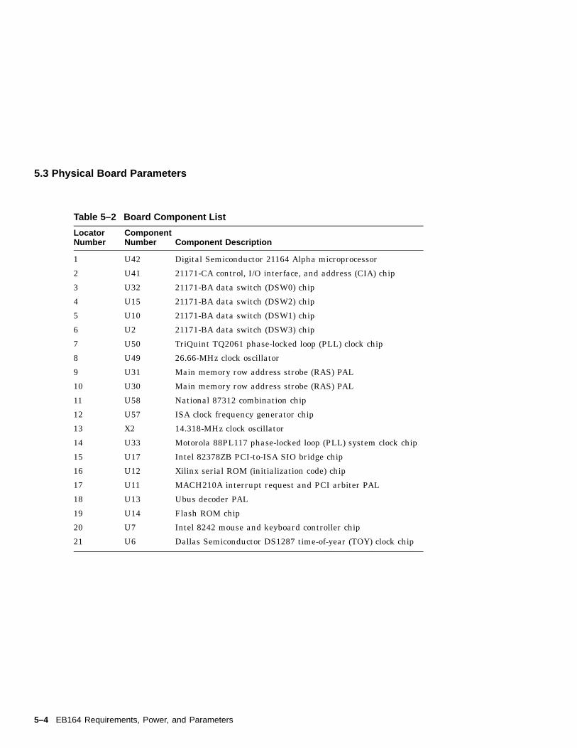
5.3 Physical Board Parameters
Table 5–2 Board Component List
LocatorNumber
ComponentNumber Component Description
1 U42 Digital Semiconductor 21164 Alpha microprocessor
2 U41 21171-CA control, I/O interface, and address (CIA) chip
3 U32 21171-BA data switch (DSW0) chip
4 U15 21171-BA data switch (DSW2) chip
5 U10 21171-BA data switch (DSW1) chip
6 U2 21171-BA data switch (DSW3) chip
7 U50 TriQuint TQ2061 phase-locked loop (PLL) clock chip
8 U49 26.66-MHz clock oscillator
9 U31 Main memory row address strobe (RAS) PAL
10 U30 Main memory row address strobe (RAS) PAL
11 U58 National 87312 combination chip
12 U57 ISA clock frequency generator chip
13 X2 14.318-MHz clock oscillator
14 U33 Motorola 88PL117 phase-locked loop (PLL) system clock chip
15 U17 Intel 82378ZB PCI-to-ISA SIO bridge chip
16 U12 Xilinx serial ROM (initialization code) chip
17 U11 MACH210A interrupt request and PCI arbiter PAL
18 U13 Ubus decoder PAL
19 U14 Flash ROM chip
20 U7 Intel 8242 mouse and keyboard controller chip
21 U6 Dallas Semiconductor DS1287 time-of-year (TOY) clock chip
5–4 EB164 Requirements, Power, and Parameters

ASupporting Vendor Products
To obtain components and accessories that are not included with your EB164motherboard, Digital Equipment Corporation suggests the following vendors.In doing so, Digital does not warrant these components or guarantee that theywill function in all configurations.
A.1 Products IncludedThe following products are included in the EB164 motherboard kit.
• Alpha microprocessor clock solution. Components available from:
TriQuint Semiconductor2300 Owen StreetSanta Clara CA 95054Phone: 408–982–0900 ext 142FAX: 408–982–0222
NEL Frequency (crystal oscillator source)
CPU Frequency Oscillator FrequencyTriQuint PLL PartNumber
21164-266 26.66 MHz (included) TQ2061 (included)
21164-300 30.0 MHz (not supplied) TQ2061 (included)
21164-333 33.33 MHz (not supplied) TQ2061 (included)
• Heat sink and fan solution. Components included: heat sink, GRAFOILpad, 2 hex nuts, heat sink clips, 60-mm fan, fan guard, and 4 screws.Components available from:
United Machine and Tool DesignRiver RoadFremont NH 03044Phone 603–642–5040FAX 603–642–5819
Supporting Vendor Products A–1

A.1 Products Included
• Bcache (Level 3) cache SIMMs
Cache SizeSIMMConfiguration Qty Vendor/Part Number
2MB @10 ns 128K � 80 2 Digital PN, 21A04-M1
A.2 Products Not IncludedThe following products are not included in the EB164 motherboard kit.
• DRAM system memory—70 ns DRAM SIMMs (5 V, 72 pin)1M � 36, 2M � 36, 4M � 36, 8M � 36, 16M � 36.
Note
The DRAM SIMMs must be n � 36 SIMMs.
• Power supply—+3.3 V, +5 V, –5 V, +12 V, –12 V, available from:
Emacs Electronics USA, Inc.1410 Gail Borden Place C-4El Paso TX 79935Phone: 915–599–2688Part number: AP2-5300F (300 W)
Autec Power Systems69 Moreland RdSimi Valley, CA 93065Phone: 805–522–0888Part number: PCB-3330-1010-D (339 W)
• EnclosureAxxion part number TL17 (modified for Digital applications).
A–2 Supporting Vendor Products

BTechnical Support and Ordering
Information
B.1 Obtaining Technical SupportIf you need technical support or help deciding which literature best meets yourneeds, call the Digital Semiconductor Information Line:
United States and CanadaOutside North America
1–800–332–2717+1–508–628–4760
B.2 Ordering Digital Semiconductor ProductsTo order the EB164, contact your local distributor.
The following table lists some of the semiconductor products available fromDigital. To obtain a Digital Semiconductor Product Catalog, contact the DigitalSemiconductor Information Line.
Product Order Number
Digital Semiconductor 21164 Alpha Microprocessor Motherboard(EB164) 266-MHz Kit(Supports the Windows NT operating system.)
21A04-A0
Digital Semiconductor 21164 333-MHz Alpha Microprocessor 21164–333
Digital Semiconductor 21164 300-MHz Alpha Microprocessor 21164–300
Digital Semiconductor 21164 266-MHz Alpha Microprocessor 21164–266
Digital Semiconductor 21164 266-MHz Alpha Microprocessor forWindows NT
21164–P1
Technical Support and Ordering Information B–1

B.3 Ordering Digital Semiconductor Literature
B.3 Ordering Digital Semiconductor LiteratureThe following table lists some of the available Digital Semiconductor literature.For a complete list, contact the Digital Semiconductor Information Line.
Title Order Number
Alpha AXP Architecture Reference Manual1 EY–T132E–DP
Alpha AXP Architecture Handbook EC–QD2KA–TE
Alpha 21164 Microprocessor Data Sheet EC–QAEPC–TE
Alpha 21164 Microprocessor Hardware Reference Manual EC–QAEQC–TE
Alpha 21164 Microprocessor Product Brief EC–QAENB–TE
Alpha 21164 Microprocessor Evaluation Board Read MeFirst
EC–QD2VB–TE
Alpha 21164 Microprocessor Evaluation Board ProductBrief
EC–QCZZD–TE
Digital Semiconductor 21164 Alpha MicroprocessorEvaluation Board User’s Guide
EC–QD2UD–TE
DECchip 21171 Core Logic Chipset Product Brief EC–QC3EB–TE
DECchip 21171 Core Logic Chipset Technical ReferenceManual
EC–QE18B–TE
Answers to Common Questions about PALcode for AlphaAXP Systems
EC–N0647–72
PALcode for Alpha Microprocessors System Design Guide EC–QFGLB–TE
Alpha Microprocessors Evaluation Board Windows NT3.51 Installation Guide
EC–QLUAD–TE
SPICE Models for Alpha Microprocessors and PeripheralChips: An Application Note
EC–QA4XC–TE
Alpha Microprocessors SROM Mini-Debugger User’sGuide
EC–QHUXA–TE
Alpha Microprocessors Evaluation Board Debug MonitorUser’s Guide
EC–QHUVC–TE
Alpha Microprocessors Evaluation Board Software DesignTools User’s Guide
EC–QHUWA–TE
1To purchase the Alpha AXP Architecture Reference Manual, call 1–800–DIGITAL from the U.S. orCanada, contact your local Digital office, or call Digital Press at 1–800–366–2665.
B–2 Technical Support and Ordering Information
B.4 Ordering Third-Party Literature
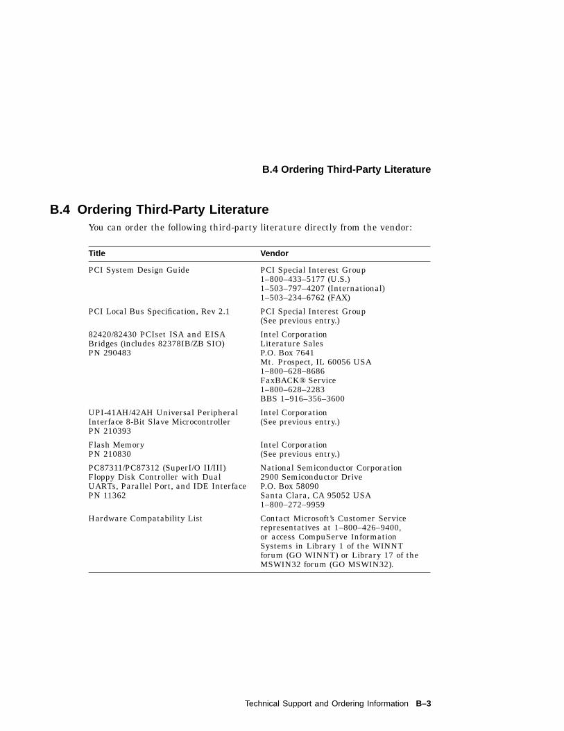
B.4 Ordering Third-Party LiteratureYou can order the following third-party literature directly from the vendor:
Title Vendor
PCI System Design Guide PCI Special Interest Group1–800–433–5177 (U.S.)1–503–797–4207 (International)1–503–234–6762 (FAX)
PCI Local Bus Specification, Rev 2.1 PCI Special Interest Group(See previous entry.)
82420/82430 PCIset ISA and EISABridges (includes 82378IB/ZB SIO)PN 290483
Intel CorporationLiterature SalesP.O. Box 7641Mt. Prospect, IL 60056 USA1–800–628–8686FaxBACK® Service1–800–628–2283BBS 1–916–356–3600
UPI-41AH/42AH Universal PeripheralInterface 8-Bit Slave MicrocontrollerPN 210393
Intel Corporation(See previous entry.)
Flash MemoryPN 210830
Intel Corporation(See previous entry.)
PC87311/PC87312 (SuperI/O II/III)Floppy Disk Controller with DualUARTs, Parallel Port, and IDE InterfacePN 11362
National Semiconductor Corporation2900 Semiconductor DriveP.O. Box 58090Santa Clara, CA 95052 USA1–800–272–9959
Hardware Compatability List Contact Microsoft’s Customer Servicerepresentatives at 1–800–426–9400,or access CompuServe InformationSystems in Library 1 of the WINNTforum (GO WINNT) or Library 17 of theMSWIN32 forum (GO MSWIN32).
Technical Support and Ordering Information B–3


Index
AAirflow requirements, 5–2Alpha
documentation, B–2Arbitration scheme, 4–5Associated literature, B–2
BBackup cache
See BcacheBcache
Digital part number, A–2index jumpers, 2–5SIMM connectors, 2–10size jumpers, 2–4speed jumpers, 2–5subsystem, 1–3
BC_RD_FAST jumper, 2–7Block diagram, 1–1
interrupt logic, 4–1power distribution, 4–5
Boardconfiguration, 2–1connectors, 2–8jumpers, 2–1
Boot option jumper, 2–6Bridge
See SIO chip
CCache
See Bcache21171 chipset, 1–1Chipset support, 1–1Clock divisor jumper, 2–4COM1 connector, 2–11COM2 connector, 2–11Components
See System componentsConfiguration, 2–1 to 2–14
hardware, 3–2software, 3–8
Configuration jumpers, 2–1Connectors, 2–8
Bcache SIMM, 2–10CPU fan power, 2–14CPU fan sensor, 2–14debug monitor interface, 2–11diskette, 2–11DRAM SIMM, 2–10IDE drive, 2–11ISA bus, 2–10keyboard, 2–10Mini-Debugger, 2–11mouse, 2–11parallel port, 2–11PCI bus, 2–10power, 2–13, 2–14serial interface ports, 2–11speaker, 2–12SROM port, 2–11system enclosure fan power, 2–11
Index–1

Conventions, viiiCooling fan, CPU
power connectors, 2–14sensor connector, 2–14
Currentdc ampere requirements, 5–1
Ddc power distribution, 4–5
See also Power requirementsdc power requirements, 5–1Debug and monitor ROM
system support, 1–5Debug monitor, 3–8
interface connector, 2–11Digital Semiconductor 21171 chipset, 1–1Diskette drive, 1–8
connector, 2–11controller, 1–4hardware requirement, 3–2installation, 3–6
Documentation, B–2DRAM
SIMM connectors, 2–10Dynamic RAM
See DRAM
EEnvironmental requirements, 5–2
FFan, CPU
See Heat sink fanFan, heat sink
See Heat sink fanFan, system enclosure
See System enclosure fanFeatures
See System features
Flash ROM, 1–5developing code, 1–4loading code, 1–4write-enable jumper, 2–7write-protect jumper, 2–7
Floppy driveSee Diskette drive
Functional description, 4–1 to 4–13dc power distribution, 4–5 to 4–7interrupts, 4–1 to 4–4ISA bus devices, 4–5PCI devices, 4–7
GGRAFOIL pad, 3–4
HHalt button, 2–12Hard drive connector, 2–11Hardware requirements, 3–1 to 3–2Heat sink, 3–3, 3–4, 3–5Heat sink fan, 3–3, 3–4, 3–5
CPU environment, 5–2power connectors, 2–14sensor, 5–1sensor connector, 2–14
IIDE, 4–5
drive active pins, 2–11drive cable, 3–8drive connector, 2–11interface, 1–4, 1–8
Industry Standard ArchitectureSee ISA
Integrated device electronicsSee IDE
Interrupt mask registers, 4–4Interrupts, 4–1ISA
arbitration, 4–5bus connectors, 2–10
Index–2

ISA (cont’d)devices, 4–5interface overview, 1–4
JJumpers, 2–1
Bcache index, 2–5Bcache size, 2–4Bcache speed, 2–5BC_RD_FAST, 2–7boot option, 2–6Flash ROM write-protect/write-enable,
2–7Mini-Debugger, 2–6system clock divisor, 2–4system configuration, 2–1
KKeyboard
connector, 2–10lock switch, 2–12
LL3 cache
See BcacheLevel 3 cache
See BcacheLiterature, B–2, B–3
MMemory
SIMM connectors, 2–10Memory subsystem, 1–3
See also DRAMMini-Debugger
connector, 2–11jumper, 2–6
Mouse connector, 2–11
OOperating systems
flash ROM support, 1–4software support, 1–5supported operating systems, 1–7
Ordering products, B–1
PParallel port connector, 2–11Parts
ordering, B–1PCI
arbitration, 4–5bus connectors, 2–10devices, 4–7interface overview, 1–3
Peripheral component interconnectSee PCI
Physical boardcomponent layout, 5–2parameters, 5–2
Power connectors, 2–13, 2–14Power distribution, 4–5Power on indicator, 2–12Power requirements, 5–1
See also Power distributionPower supply
dc ampere requirements, 5–1wattage requirements, 5–1
RRAM
See DRAM; SRAMRegisters
interrupt mask, 4–4Related documentation, B–2Reset button, 2–12ROM
See Flash ROM; Serial ROM (SROM)
Index–3

SSaturn I/O chip
See SIO chipSemiconductor Information Line, B–1Serial interface connectors, 2–11Serial ROM
See SROMSIMM
connectors, 2–10Single inline memory module
See SIMMSIO chip, 1–3, 4–3, B–3Software requirements, 3–2Software support, 1–5Speaker connection pins, 2–12SRAM, 1–3, 2–6, 2–10, 3–1, 3–6SROM
code, 1–5connector, 2–11system support, 1–5
Static RAMSee SRAM
Support chipset, 1–1System components, 1–1System enclosure fan
power connectors, 2–11System features, 1–1
System I/O chipSee SIO chip
System ROMSee Flash ROM
System softwaresoftware support, 1–5
TTechnical support, B–1Third-party documentation, B–3Tools, 3–3
UUART, 1–4Ubus, 4–5Universal asynchronous receiver–transmitter
See UARTUtility bus
See Ubus
VVendor products, A–1
WWindows NT ARC firmware, 3–8
Index–4