Embed Size (px)
Citation preview

PPPPPentek, Inc.entek, Inc.entek, Inc.entek, Inc.entek, Inc. • One Park Way, Upper Saddle River, NJ 07458 • Tel: (201) 818-5900 • Fax: (201) 818-5904 • Email: [email protected] • http://www.pentek.com
11111
Digital Receiver Handbook: Basics of Software Radio
Digital Receiver Handbook:Basics of Software Radio
Fifth Edition
PPPPPentek, Inc.entek, Inc.entek, Inc.entek, Inc.entek, Inc.One Park Way, Upper Saddle River, New Jersey 07458
Tel: (201) 818-5900 • Fax: (201) 818-5904Email: [email protected] • http://www.pentek.com
Copyright © 1998, 2001, 2003, 2006 Pentek Inc.All rights reserved.
Contents of this publication may not be reproduced in any form without written permission.Specifications are subject to change without notice.
Pentek, GateFlow, ReadyFow and VIM are registered trademarks of Pentek, Inc.
TheorTheorTheorTheorTheory of Operationy of Operationy of Operationy of Operationy of Operation
ApplicationsApplicationsApplicationsApplicationsApplications
PPPPProductsroductsroductsroductsroductsby
RRRRRodger Hodger Hodger Hodger Hodger H. Hosking. Hosking. Hosking. Hosking. HoskingVice-President & Cofounder of Pentek, Inc.
®

PPPPPentek, Inc.entek, Inc.entek, Inc.entek, Inc.entek, Inc. • One Park Way, Upper Saddle River, NJ 07458 • Tel: (201) 818-5900 • Fax: (201) 818-5904 • Email: [email protected] • http://www.pentek.com
22222
Digital Receiver Handbook: Basics of Software Radio
Preface
Digital receivers have revolutionized electronic systems for avariety of applications including communications, data acquisition and signal processing.
This handbook shows how digital receivers, the fundamental building block for software radio,can replace conventional analog receiver designs, offering significant benefits in performance, density and cost.
In order to fully appreciate the benefits of digital receivers, a conventional analog receiversystem will be compared to its digital receiver counterpart, highlighting similarities and differences.
The inner workings of the digital receiver will be explored with an in-depth description of the internalstructure and the devices used. Finally, some actual receiver system implementations and available
off-the-shelf board level digital receiver products for embedded systems will be described.

PPPPPentek, Inc.entek, Inc.entek, Inc.entek, Inc.entek, Inc. • One Park Way, Upper Saddle River, NJ 07458 • Tel: (201) 818-5900 • Fax: (201) 818-5904 • Email: [email protected] • http://www.pentek.com
33333
Digital Receiver Handbook: Basics of Software Radio
Figure 1
The conventional heterodyne radio receiver, as seenin Figure 1, has been in use for nearly a century. Let’sreview the structure of the analog receiver so comparisonto the digital receiver becomes apparent.
First the RF signal from the antenna is amplified,typically with a tuned RF stage, that amplifies a regionof the frequency band of interest.
This amplified RF signal is then fed into a mixerstage. The other input to the mixer comes from the localoscillator whose frequency is controlled by the tuningknob on the radio.
The mixer translates the desired input signal to theIF (Intermediate Frequency). See Figure 2.
The IF stage is a bandpass amplifier that only letsone signal or radio station through. Common centerfrequencies for IF stages are 455 kHz and 10.7 MHzfor commercial AM and FM broadcasts.
The demodulator recovers the original modulatingsignal from the IF output using one of several differentschemes.
For example, AM uses an envelope detector and FMuses a frequency discriminator. In a typical home radio,the demodulated output is fed to an audio amplifierwhich drives a speaker.
Figure 2
Analog RAnalog RAnalog RAnalog RAnalog Receiver Block Diagrameceiver Block Diagrameceiver Block Diagrameceiver Block Diagrameceiver Block Diagram Analog RAnalog RAnalog RAnalog RAnalog Receiver Mixingeceiver Mixingeceiver Mixingeceiver Mixingeceiver Mixing
The mixer performs an analog multiplication of thetwo inputs and generates a difference frequency signal.
The frequency of the local oscillator is set so thatthe difference between the local oscillator frequency anddesired input signal (the radio station you want toreceive) equals the IF.
For example, if you wanted to receive an FMstation at 100.7 MHz and the IF is 10.7 MHz, you wouldtune the local oscillator to:
100.7 - 10.7 = 90 MHz
This is called “downconversion” or “translation”because a signal at a high frequency is shifted down to alower frequency by the mixer.
The IF stage acts as a narrowband filter which onlypasses a “slice” of the translated RF input. The band-width of the IF stage is equal to the bandwidth of thesignal (or the “radio station”) that you are trying toreceive.
For commercial FM, the bandwidth is about100 kHz and for AM it is about 5 kHz. This is consis-tent with channel spacings of 200 kHz and 10 kHz,respectively.
TheorTheorTheorTheorTheory of Operationy of Operationy of Operationy of Operationy of Operation

PPPPPentek, Inc.entek, Inc.entek, Inc.entek, Inc.entek, Inc. • One Park Way, Upper Saddle River, NJ 07458 • Tel: (201) 818-5900 • Fax: (201) 818-5904 • Email: [email protected] • http://www.pentek.com
44444
Digital Receiver Handbook: Basics of Software Radio
Figure 3 Figure 4
Digital RDigital RDigital RDigital RDigital Receiver Block Diagrameceiver Block Diagrameceiver Block Diagrameceiver Block Diagrameceiver Block Diagram
Take a look at the digital receiver block diagramshown in Figure 3. Note the strong similarity to theanalog receiver diagram—all of the basic principles ofanalog receivers still apply.
Right after the RF amplifier and an optional RFtranslator stage, we use an A/D (analog-to-digital)converter to digitize the RF input into digital samplesfor the subsequent mixing, filtering and demodulationthat are performed using digital signal processingelements.
Before we continue, lets first review a theoremfundamental to sampled data which lays the foundationfor the A/D converter requirements.
Nyquist’s Theorem:
“Any signal can be represented by discrete samplesif the sampling rate is at least twice the bandwidth of thesignal.”
For example, if we use an A/D converter samplingat 70 MHz, then the bandwidth of the analog inputmust be less than 35 MHz.
Now let’s see what happens if we ignore Nyquist’scriterion.
AliasingAliasingAliasingAliasingAliasing
Figure 4 shows a frequency display of a systembeing sampled at frequency fs. For all input signalsbelow fs/2, such as the one at fo, we fully meet theNyquist criterion. In fact, any number of signals can bepresent in the shaded region and all will be correctlyrepresented in the sampled data.
But if we have a signal present at say, fa, which isabove fs/2, the sampling process will generate an aliasedimage which will appear in the sampled data at fs - fa.This image cannot be distinguished from a true signalwhich might have been present at that same frequency.
The point is this: once an aliased image is created inthe sampling process, no amount of further processingcan distinguish between a true signal and an aliasedsignal. Therefore, it is imperative to prevent aliasingbefore it occurs.
TheorTheorTheorTheorTheory of Operationy of Operationy of Operationy of Operationy of Operation

PPPPPentek, Inc.entek, Inc.entek, Inc.entek, Inc.entek, Inc. • One Park Way, Upper Saddle River, NJ 07458 • Tel: (201) 818-5900 • Fax: (201) 818-5904 • Email: [email protected] • http://www.pentek.com
55555
Digital Receiver Handbook: Basics of Software Radio
Figure 5 Figure 6
Anti-Anti-Anti-Anti-Anti-Aliasing FAliasing FAliasing FAliasing FAliasing Filterilterilterilterilter
The most straightforward way to prevent aliasing isto use a low pass filter before the A/D converter whichremoves all signals above fs/2.
This filter, called an anti-aliasing filter, is seen inFigure 5. Now the signal at fa is blocked so the A/Dconverter never sees it.
Anti-aliasing filters are often included on the sameboard as the A/D converter as a convenience to the user.
As a side note, Nyquist’s criterion can also be metby limiting the bandwidth of the sampled signal usingother types of filters.
For example, suppose we really wanted to receivesignals between fs/2 and fs in the above diagram. If weused a bandpass filter with a passband from fs/2 to fs, wewould fully meet the Nyquist criterion because thebandwidth is equal to one half the sampling rate.
Once the sampling is done, the band of signalsfrom fs/2 to fs is “folded” into the frequency band fromDC to fs/2. This half-sampling frequency is often calledthe “folding frequency.”
This technique is sometimes called “undersampling”and while this works well in theory, care must be takenin actual practice to ensure that the A/D convertersupports the higher input frequencies it must handle.
Digital RDigital RDigital RDigital RDigital Receiver Block Diagrameceiver Block Diagrameceiver Block Diagrameceiver Block Diagrameceiver Block Diagram
Looking again at the overall block diagram, thedigital samples coming out of the A/D converter arebeing fed to the next stage which is the digital receiverchip—in the dotted line, as shown in Figure 6.
The digital receiver chip is typically contained on asingle monolithic chip which forms the heart of thedigital receiver system. It is also sometimes referred to asa digital downconverter (DDC) or a digital dropreceiver (DDR).
Inside the digital receiver chip there are three majorsections:
• Local Oscillator
• Mixer
• Decimating Low Pass Filter
Note that the inputs to the digital chip are thedigital samples from the A/D and the A/D sampleclock. With a 70 MHz A/D, samples are fed into thischip and processed in real time at rates up to 70 MHz!
We will now explore each section of the digitalreceiver system shown in Figure 6, starting with thedigital local oscillator.
TheorTheorTheorTheorTheory of Operationy of Operationy of Operationy of Operationy of Operation

PPPPPentek, Inc.entek, Inc.entek, Inc.entek, Inc.entek, Inc. • One Park Way, Upper Saddle River, NJ 07458 • Tel: (201) 818-5900 • Fax: (201) 818-5904 • Email: [email protected] • http://www.pentek.com
66666
Digital Receiver Handbook: Basics of Software Radio
Figure 7 Figure 8
The Local Oscillator has very impressive frequencyswitching characteristics as shown in Figure 8.
When switching between two frequencies, thedigital accumulator precisely maintains the phase of thesine and cosine outputs for phase-continuous switching.When the frequency is changed, what actually changesis the amount of phase advance per sample.
This allows the local oscillator to perform FSK(frequency shift keying) and very finely resolved sweeps.Transients and settling normally associated with othertypes of local oscillators, such as phase-locked loopsynthesizers, are eliminated.
The time it takes to retune the local oscillator issimply the time it takes to load a new digital frequencyword (32-bit binary number) into a register, usually wellbelow one microsecond.
Some digital receiver chips employ a local oscillatorwith a built-in “chirp” function. This is a fast, program-mable and precise frequency sweep which is very usefulin radar systems.
First, let’s explore the Local Oscillator highlightedin Figure 7. It’s a direct digital frequency synthesizer(DDS) sometimes called a numerically controlledoscillator (NCO). This device is implemented entirelywith digital circuitry.
The oscillator generates digital samples of two sinewaves precisely offset by 90 degrees in phase, creatingsine and cosine signals. It uses a digital phase accumula-tor and sine/cosine lookup tables.
Note that the A/D clock is fed into the localoscillator. The digital samples out of the local oscillatorare generated at a sampling frequency exactly equal to theA/D sample clock frequency, fs.
It is important to understand that the output samplingrate is always fixed at fs, regardless of the frequency setting.The sine/cosine output frequency is changed by programmingthe amount of phase advance per sample.
A small phase advance per sample corresponds to alow frequency and a large advance to a high frequency. Thephase advance per sample is directly proportional to theoutput frequency and is programmable from DC to fs/2with up to 32-bit of resolution.
Using a 70 MHz sampling clock, the frequencyrange is from DC to 35 MHz and the resolution is wellbelow 1Hz.
LLLLLocal Oscillatorocal Oscillatorocal Oscillatorocal Oscillatorocal Oscillator Phase Continuous SwitchingPhase Continuous SwitchingPhase Continuous SwitchingPhase Continuous SwitchingPhase Continuous Switching
TheorTheorTheorTheorTheory of Operationy of Operationy of Operationy of Operationy of Operation

PPPPPentek, Inc.entek, Inc.entek, Inc.entek, Inc.entek, Inc. • One Park Way, Upper Saddle River, NJ 07458 • Tel: (201) 818-5900 • Fax: (201) 818-5904 • Email: [email protected] • http://www.pentek.com
77777
Digital Receiver Handbook: Basics of Software Radio
Figure 9 Figure 10
Let’s look at the “difference” mixer product in thefrequency domain as shown in Figure 10. At the outputof the mixer, the high frequency wideband signals in theA/D input have been translated down to DC with ashift or offset equal to the local oscillator frequency.
This is similar to the analog receiver mixer exceptthat the analog receiver mixes the RF input down to anIF (intermediate frequency).
In the digital receiver, the precision afforded by thedigital signal processing allows us to mix right down tobaseband (or 0 Hz). Overlapping mixer images, difficultto reduce with analog mixers, are strongly rejected bythe accuracy of the sine and cosine local oscillatorsamples and the mathematical precision of the multipli-ers in the digital mixer.
By tuning the local oscillator over its frequencyrange, any portion of the RF input signal can betranslated down to DC. In effect, the wideband RFsignal spectrum can be shifted around 0 Hz, left andright, simply by changing the local oscillator frequency.
The objective is to tune the local oscillator to centerthe signal of interest around 0 Hz so that the low passfilter that follows can pass only the signal of interest.
The next major component of the digital receiverchip is the Mixer seen in Figure 9. The Mixer actuallyconsists of two digital multipliers. Digital input samplesfrom the A/D are mathematically multiplied by thedigital sine and cosine samples from the local oscillator.
Note that the input A/D data samples and the sineand cosine samples from the local oscillator are beinggenerated at the same rate, namely, once every A/Dsample clock. Since the data rates into both inputs ofthe mixers are the A/D sampling rate fs, the multipliersalso operate at that same rate and produce multipliedoutput product samples at fs.
The sine and cosine inputs from the local oscillatorcreate I and Q (in-phase and quadrature) outputs thatare important for maintaining phase information containedin the input signal. From a signal standpoint, themixing produces a single-sideband complex translationof the real input.
Unlike analog mixers which also generate manyunwanted mixer products, the digital mixer is nearly idealand produces only two outputs: the sum and differencefrequency signals.
Digital MixerDigital MixerDigital MixerDigital MixerDigital Mixer Digital RDigital RDigital RDigital RDigital Receiver Mixer Teceiver Mixer Teceiver Mixer Teceiver Mixer Teceiver Mixer Translationranslationranslationranslationranslation
TheorTheorTheorTheorTheory of Operationy of Operationy of Operationy of Operationy of Operation

PPPPPentek, Inc.entek, Inc.entek, Inc.entek, Inc.entek, Inc. • One Park Way, Upper Saddle River, NJ 07458 • Tel: (201) 818-5900 • Fax: (201) 818-5904 • Email: [email protected] • http://www.pentek.com
88888
Digital Receiver Handbook: Basics of Software Radio
Figure 11 Figure 12
Once the RF signal has been translated, it is nowready for filtering.
The decimating low pass filter accepts input samplesfrom the mixer output at the full A/D sampling frequencyfs. It utilizes digital signal processing to implement anFIR (Finite Impulse Response) filter transfer function.
The filter passes all signals from 0 Hz up to aprogrammable cutoff frequency or bandwidth, andrejects all signals above that cutoff frequency.
This digital filter is a complex filter which processesboth I and Q signals from the mixer. At the output youcan select either I and Q (complex) values or just realvalues, depending on your system requirements.
Figure 12 shows a representation of the action ofthe filter in the frequency domain. The filter passes onlysignals from 0 Hz up to the filter bandwidth. All higherfrequencies have been removed.
Remember, the wideband input signal was translateddown to DC by the mixer and positioned around 0 Hzby the tuning frequency of the local oscillator.
Now, at the filter output we have effectively selecteda narrow slice of the RF input signal and translated it toDC. Note that we have blocked all other signals aboveand below the band of interest.
The bandlimiting action of the filter is analogous tothe action of the IF stage in the analog receiver, exceptthat the decimating low pass filter operates around DCinstead of being centered at an IF frequency.
Decimating LDecimating LDecimating LDecimating LDecimating Low Pow Pow Pow Pow Pass Fass Fass Fass Fass Filterilterilterilterilter Decimating FDecimating FDecimating FDecimating FDecimating Filter Bandlimitingilter Bandlimitingilter Bandlimitingilter Bandlimitingilter Bandlimiting
TheorTheorTheorTheorTheory of Operationy of Operationy of Operationy of Operationy of Operation

PPPPPentek, Inc.entek, Inc.entek, Inc.entek, Inc.entek, Inc. • One Park Way, Upper Saddle River, NJ 07458 • Tel: (201) 818-5900 • Fax: (201) 818-5904 • Email: [email protected] • http://www.pentek.com
99999
Digital Receiver Handbook: Basics of Software Radio
Figure 13
FFFFFrequency Zoomrequency Zoomrequency Zoomrequency Zoomrequency Zoom Decimation FDecimation FDecimation FDecimation FDecimation Factor = Nactor = Nactor = Nactor = Nactor = N
In order to set the bandwidth of the filter, you needto program a parameter called the decimation factor asseen in Figure 14. Since the output bandwidth and theoutput sampling rate are directly related in the DDC,the decimation factor also sets the output sampling rate.
The decimation factor, N, determines the ratiobetween input and output sampling rates and also theratio between input and output bandwidths. Note thatthe output sampling rate for real outputs is twice thatfor complex outputs.
For example, if you have an input sampling rate of70 MHz and a desired nominal output bandwidth of 7kHz, the decimation should be set for 10,000. Theoutput sampling rate would be 7 kHz for complexoutputs and 14 kHz for real outputs.
Note that the usable bandwidth is always less than theNyquist bandwidth, hence in the previous example we seea real input bandwidth of about 30 MHz (with a 70 MHzsampling rate) and an output bandwidth of about 6kHz (with a complex output sampling rate of 7 kHz ora 14 kHz output for real).
Digital receivers can be divided into two classes,narrowband and wideband, distinguished by theprogrammable range of decimation factors.
Narrowband receivers typically have a range ofdecimation factors from 32 or 64 to 65,536 or 131,072,depending on the chip manufacturer.
Wideband receivers typically have a range ofdecimation factors from 2 to 64.
As an example, take a look at an actual frequencydisplay shown in Figure 13. The top figure shows a30 MHz wideband RF input which was sampled by theA/D converter at 70 MHz.
Suppose we have a signal of interest at 20 MHz andwe know that the bandwidth of the signal is 6 kHz.
By setting the local oscillator to 20 MHz and thebandwidth of the filter to 6 kHz we can translate thesignal and extract only a 6 kHz band as shown in thebottom figure.
Note that the input band around 20 MHz has beentranslated down to DC and the complex output allowsus to compute a complex FFT power spectrum centeredat 0 Hz. Frequency components which were previouslyabove 20 MHz are now to the right of 0 Hz and thosebelow 20 MHz are to the left of 0 Hz. The 20 MHzcarrier signal is now at 0 Hz exactly.
In this case, we have used the decimating low passfilter to perform a dramatic reduction in the signalbandwidth from 30 MHz down to 6 kHz. The samplingrate has also been reduced from 70 MHz to 7 kHz, afactor of 10,000!
Next, let’s see exactly how to control the bandwidthof the FIR filter.
Figure 14
TheorTheorTheorTheorTheory of Operationy of Operationy of Operationy of Operationy of Operation

PPPPPentek, Inc.entek, Inc.entek, Inc.entek, Inc.entek, Inc. • One Park Way, Upper Saddle River, NJ 07458 • Tel: (201) 818-5900 • Fax: (201) 818-5904 • Email: [email protected] • http://www.pentek.com
1010101010
Digital Receiver Handbook: Basics of Software Radio
Figure 15
FPGA Implementation of Digital RFPGA Implementation of Digital RFPGA Implementation of Digital RFPGA Implementation of Digital RFPGA Implementation of Digital Receiverseceiverseceiverseceiverseceivers
FPGAs (Field Programmable Gate Arrays) havebecome more appropriate for implementing digitalreceiver functions because of the built-in hardwaremultipliers and generous RAM. Remember that thedigital mixer section is nothing more than a hardwaremultiplier. The FIR filter also uses one multiplier foreach filter tap plus RAM for delay memory.
The Pentek GateFlow® IP Core Library for softwareradio includes fast FFT engines, radar pulse compres-sors, and digital receivers. These cores allow FPGAdesigners to readily incorporate these highly optimizedfunctions in FPGA-based products.
Most of Pentek’s recent software radio productsinclude user-configurable FPGAs in the signal path tosupport IP cores and custom DSP algorithms. Pentekalso offers factory installation of IP cores in several ofthese products, thereby eliminating the FPGA designeffort and allowing customers to easily take advantage ofthis exciting new technology.
Figure 15 above shows a dual channel A/Dconverter VIM-2 module with the Pentek GateFlowWideband Receiver Core 421 installed. This core replacesthe TI / GC1012B chip and offers higher dynamicrange and user-programmable FIR coefficients. It accepts16-bit inputs instead of the 12-bit inputs of the ASIC totake full advantage of the 14-bit A/D converters. For thelatest FPGA offerings visit the online FPGA Resource atpentek.com/gateflow.
FPGAs TFPGAs TFPGAs TFPGAs TFPGAs Tackle DSP Fackle DSP Fackle DSP Fackle DSP Fackle DSP Functionsunctionsunctionsunctionsunctions
FPGAs not only offer significant advantages asspecialized replacements for standard ASIC digitalreceivers, they also provide extremely high performancesignal processing capabilities to offload these tasks fromDSP and RISC processors.
An example is the Pentek GateFlow IP Core 4044k-point complex FFT. Although all GateFlow IP Coresare designed for use on any Virtex-II, Virtex-II Pro orSpartan 3 product, the Core 404 is available as a factoryinstalled option on the Model 6236 Dual ChannelReceiver VIM-2 module shown in Figure 16.
In this case, real data from the A/D converter orcomplex I and Q samples from the wideband digitalreceiver can be directed into the FFT engine. The firststage performs an optional Hanning (or other) windowingfunction as a preprocessing step before the complex4k-point FFT.
The output of the FFT can be optionally convertedto power by summing I2 and Q2. Finally, consecutiveoutputs can be optionally averaged to reduce widebandnoise.
Because of the highly-parallel architecture of this IPCore, it can sustain real time input sampling rates ofup to 160 MHz. It would take approximately eight G4PowerPCs running at 1 GHz to equal the processingpower of this impressive engine!
Figure 16
TheorTheorTheorTheorTheory of Operationy of Operationy of Operationy of Operationy of Operation

PPPPPentek, Inc.entek, Inc.entek, Inc.entek, Inc.entek, Inc. • One Park Way, Upper Saddle River, NJ 07458 • Tel: (201) 818-5900 • Fax: (201) 818-5904 • Email: [email protected] • http://www.pentek.com
1111111111
Digital Receiver Handbook: Basics of Software Radio
Figure 18
Returning to our overall digital receiver blockdiagram shown in Figure 18, our output signal is nowtranslated, filtered and bandlimited and is ready forfurther processing.
Note that the output signal from the decimatinglow pass filter is still a sampled time signal which couldrepresent any kind of modulated or unmodulated signal.We could send this signal directly to a D/A converter,producing an analog waveform.
For straight single-sideband frequency divisionmultiplexed speech, for example, we could now connectthe D/A output to a speaker and listen to the selectedvoice channel directly.
In many systems, further processing is required, aswith modem demodulation for example. Since theoutput of the digital receiver is now at a much lowersampling rate than the original wideband input signal,this additional modem processing can now be readilyhandled by a DSP or an FPGA.
Digital RDigital RDigital RDigital RDigital Receiver Block Diagrameceiver Block Diagrameceiver Block Diagrameceiver Block Diagrameceiver Block Diagram
To review, the digital receiver chip performs twomajor signal processing operations controlled by twoprogrammable parameters (Figure 17):
1) Translation of the input signal down to DC iscontrolled by setting the tuning frequency of thelocal oscillator.
2) Low pass filtering bandwidth and outputsampling rate are both controlled by setting thedecimation factor.
Because everything inside the decimating low passfilter is performed with digital circuitry and DSPtechniques, there are no undesirable effects normallyassociated with conventional analog filters.
There are no initial component tolerance ortemperature variations or aging characteristics. Nocalibration or preventive maintenance is required. Thisprovides excellent channel-to-channel matching forapplications where phase variation between channels isimportant, such as direction finding.
The FIR digital filters used have linear phase for well-behaved transient response. The filter bandwidth isprogrammable over a wide range (1000 to 1), with absolutelypredictable and uniform response throughout.
Lastly, the signal is tailored precisely for DSPprocessing by preselecting only the signal of interestthrough bandlimiting and providing it to the DSP atthe optimum sampling rate.
TTTTTwowowowowo-Step Signal P-Step Signal P-Step Signal P-Step Signal P-Step Signal Processingrocessingrocessingrocessingrocessing
TheorTheorTheorTheorTheory of Operationy of Operationy of Operationy of Operationy of Operation
Figure 17

PPPPPentek, Inc.entek, Inc.entek, Inc.entek, Inc.entek, Inc. • One Park Way, Upper Saddle River, NJ 07458 • Tel: (201) 818-5900 • Fax: (201) 818-5904 • Email: [email protected] • http://www.pentek.com
1212121212
Digital Receiver Handbook: Basics of Software Radio
DSP Demodulation FDSP Demodulation FDSP Demodulation FDSP Demodulation FDSP Demodulation Functionsunctionsunctionsunctionsunctions KKKKKey Benefits of Digital Rey Benefits of Digital Rey Benefits of Digital Rey Benefits of Digital Rey Benefits of Digital Receiverseceiverseceiverseceiverseceivers
● Frequency and Phase Shift Keying (FSK, PSK)
● AM, FM, and PM
● Spread Spectrum
● Custom Frequency Agile Schemes
● Signal Analysis (FFT’s), Signal Identification
● Signal Recording and Tracking
Figure 19 Figure 20
● Dedicated digital receiver hardware
preselects only signals of interest
● Saves significant DSP horsepower
since DSP requirements are directly
proportional to sampling rate
Think of the digital receiver as a hardware preprocessorfor DSP. It preselects only the signals you are interestedin and removes all others. This provides an optimumbandwidth and minimum sampling rate into the DSP.
Since the number of DSPs required in a system isdirectly proportional to the sampling rate of inputdata, by reducing the sampling rate you can dramati-cally reduce the cost and complexity of the DSP systemthat follows.
Even if the digital receiver outputs do not require agreat deal of signal processing, reduction of bandwidthand sampling rate helps save time in data transfers toanother subsystem, helps minimize recording time andtape or disk space, and speeds up communication channels.
Virtually any form of demodulation can be imple-mented just by loading the DSP or FPGA with theappropriate algorithm (Figure 19). AM can be demodu-lated with an envelope detector, FM & PM can bedemodulated using a phase or frequency discriminatoralgorithm.
The ability to quickly change the local oscillatorallows frequency-agile modulation schemes to beaccommodated as well. Analysis functions includeenergy detection such as required by scanning receiversthat may be implemented with an FFT, for example.
Other analysis functions include cryptography,identification of transmitters based on transmissionfrequency, modulation schemes, and other signalcharacteristics.
Once the signal is successfully brought into the DSParena, automated functions such as center frequency andbandwidth tuning can be implemented to track a complexsignal which may be moving or hopping. Interestingsignals can be stored on hard disk, tape or other mediaand the time of the signal event can be logged as well.
With this arrangement, when new or proprietarydemodulation, processing, or analysis schemes are required,no new hardware is necessary. Instead, a new DSP softwarealgorithm is loaded.
TheorTheorTheorTheorTheory of Operationy of Operationy of Operationy of Operationy of Operation

PPPPPentek, Inc.entek, Inc.entek, Inc.entek, Inc.entek, Inc. • One Park Way, Upper Saddle River, NJ 07458 • Tel: (201) 818-5900 • Fax: (201) 818-5904 • Email: [email protected] • http://www.pentek.com
1313131313
Digital Receiver Handbook: Basics of Software Radio
Digital RDigital RDigital RDigital RDigital Receiver Chip Peceiver Chip Peceiver Chip Peceiver Chip Peceiver Chip Perererererformanceformanceformanceformanceformance
The above chart shows the salient characteristics forseven popular digital receiver chips and three FPGA IPcores. Note that the range of decimation settings for thenarrowband chips on the left is much higher than forthe wideband receivers on the right. The output samplingfrequencies for real and complex outputs are shown as afunction of the decimation factor N.
Notice also that the 3 dB output bandwidth of theFIR filter is expressed as a percentage of the inputsampling rate divided by N. This percentage reflects thefrequency characteristics of the specific FIR filterfunction implemented in the digital receiver chip. Eachfilter characteristic has its own passband flatness, rolloffrate, and stop band attenuation characteristics suitablefor different applications.
As an example, if we were using the TI/GC1011Awith a 64 MHz A/D converter and needed a usableoutput bandwidth of 10 kHz, we could solve for theappropriate decimation factor setting as follows:
10 kHz = 0.80 • ƒs / N orN = 0.80 • 64 MHz / 10 kHz = 5120
Note that the decimation factors of narrowbandreceivers are programmable in steps of 1 or 4 and thewideband receivers are programmable in binary steps asshown. Some receivers allow entry of custom FIR filtercoefficients and others have output resampling stages tosupport custom filter characteristics and output samplingrates.
Model numbers of Pentek products using each typeof digital receiver are shown at the bottom.
TheorTheorTheorTheorTheory of Operationy of Operationy of Operationy of Operationy of Operation
Narrowband WidebandTI / GC Intersil TI / GC Intersil TI / GC Pentek IP TI / GC Pentek IP Pentek IP
4014 50214B 1011A 50016 4016 Core 430 1012A / B Core 421 Core 422
No of Channels 4 1 1 1 4 256 1 1 1
Sample Freq (ƒs) 62.5 MHz 65 MHz 70 MHz 75 MHz 100 MHz 185 MHz 80 / 100 MHz 160 MHz 296 MHzInput bits 14/16 16 12 16 14/16 16 12 16 16Min Decim (N) 32 2 64 64 32 1024 2, 4, 8 2, 4, 8 2, 4, 8
Max Decim (N) 65k 65k 65k 131k 16k 9984 16, 32, 64 16, 32, 64 16, 32, 64Resampler No Yes No No Yes No No No NoCustom FIR Yes Yes No No Yes Yes No Yes Yes
3 dB Output BW Prog Prog 0.8ƒs/N 0.56ƒs/N Prog Prog 0.8ƒs/N Prog Prog0.9ƒs/N
VME Boards 6821 6821
6822 6822
VIM Modules 6230 6235 62506231 6235 6236 62516232 6236 6250
6251PMC Modules 7131
7140 7140
PCI Boards 76317640 7640
cPCI Boards 7231
7240 7240

PPPPPentek, Inc.entek, Inc.entek, Inc.entek, Inc.entek, Inc. • One Park Way, Upper Saddle River, NJ 07458 • Tel: (201) 818-5900 • Fax: (201) 818-5904 • Email: [email protected] • http://www.pentek.com
1414141414
Digital Receiver Handbook: Basics of Software Radio
ApplicationsApplicationsApplicationsApplicationsApplications
Applications of Digital RApplications of Digital RApplications of Digital RApplications of Digital RApplications of Digital Receiverseceiverseceiverseceiverseceivers
Digital receivers can be used in many different systems:
Tracking receivers and signal intelligence receiverscan be highly automated because digital receivers allowDSPs to perform the signal identification and analysisfunctions as well as the adaptable tuning functions.
Direction finding is an ideal application for digitalreceivers because of their excellent channel-to-channelphase matching and consistent delay characteristics.
Radar applications benefit from the tight couplingof the A/D, digital receiver and DSP functions toprocess wideband signals. FPGAs are especially wellsuited to handle FFT and pulse compression tasksnormally required in the signal processing sections.
Some of the digital receiver chips employ specialfeatures like a “chirp” sweep generator function in the localoscillator, ideal for high-performance radar applications.
Cellular phone applications are one of the strongesthigh-volume applications because of the high density oftightly-packed frequency division multiplexed voicechannels.
As a general capability, any system requiring atunable bandpass filter should be considered a candidatefor using digital receivers. Take a look at the followingapplication examples to give you some more details.
Product overviews of all models described in theapplications section are included in the last section ofthe handbook.
● Tracking Receiver System● Signal Intelligence Receiver● Direction Finding System● Radar Signal Processing System● Wireless Cellular Development System

PPPPPentek, Inc.entek, Inc.entek, Inc.entek, Inc.entek, Inc. • One Park Way, Upper Saddle River, NJ 07458 • Tel: (201) 818-5900 • Fax: (201) 818-5904 • Email: [email protected] • http://www.pentek.com
1515151515
Digital Receiver Handbook: Basics of Software Radio
TTTTTracking Rracking Rracking Rracking Rracking Receiver Systemeceiver Systemeceiver Systemeceiver Systemeceiver System
A tracking receiver locates unknown signals, locksonto them and tracks them if their frequency changes.
As shown in Figure 21, to implement this receiver,we use the 128 MB SDRAM of the Model 6821 tocreate a delay memory function.
Samples from the A/D are sent into a circular bufferwithin the SDRAM and also to a Pentek FFT IP coreimplemented in the FPGA. The spectral peaks of the FFTindicate the frequencies of signals of interest present at theinput.
The PowerPC microcontroller of the FPGA digeststhis frequency list and decides which signals to track. Itthen tunes the Pentek DDC core, also implemented in
the FPGA, accordingly. The delayed data from thecircular buffer feeds the input of this DDC core.
The digital delay can be set to match the time ittakes for the FFT energy detection and the processoralgorithm for the tuning frequency decision, so thatfrequency-agile or transient signals can be recoveredfrom their onset. The dehopped baseband output isdelivered to the rest of the system through the FPDPport or, optionally, across a VXS link.
See page 22 for a more detailed description of thePentek Model 6821 A/D Converter. This Model is alsoavailable in a dual-channel version as Model 6822, seepage 23. Both Models are available in commercial andconduction-cooled versions.
Figure 21
ApplicationsApplicationsApplicationsApplicationsApplications
System Highlights
● ● ● ● ● A/D data delivered into SDRAM that acts as a digital delay memory
● ● ● ● ● A/D data also delivered into a Pentek FFT IP core in FPGA
● ● ● ● ● FFT core detects the strength of signals at each analysis frequency
● ● ● ● ● PowerPC controller in FPGA sorts signals according to peak strenth
● ● ● ● ● PowerPC controller also tunes DDC IP core in FPGA to the strongest signal frequencies
● ● ● ● ● Delayed data from SDRAM feeds DDC IP core to compensate for FFT calculation time
● ● ● ● ● DDC captures these moving signals in real time and downconverts them to baseband
Model 6821 215 MHz A/D Converter with FPGA
Model 6821 commercial (left) andconduction-cooled version

PPPPPentek, Inc.entek, Inc.entek, Inc.entek, Inc.entek, Inc. • One Park Way, Upper Saddle River, NJ 07458 • Tel: (201) 818-5900 • Fax: (201) 818-5904 • Email: [email protected] • http://www.pentek.com
1616161616
Digital Receiver Handbook: Basics of Software Radio
Figure 22
32-32-32-32-32-Channel Signal Intelligence RChannel Signal Intelligence RChannel Signal Intelligence RChannel Signal Intelligence RChannel Signal Intelligence Receivereceivereceivereceivereceiver
This compact receiver system incorporates the entiresignal processing chain from the A/D convertersthrough digital downconversion and filtering, todecoding, demodulation and analysis performed byFPGAs and PowerPC’s. And it all fits in just a singleVMEbus slot!
The Model 6230, a 32-Channel NarrowbandReceiver, is a VIM-4 mezzanine module that includesfour 14-bit A/D converters operating at sampling ratesup to 80 MHz. All four A/D outputs are delivered toeight 4-channel receiver chips so that each of the 32narrowband channels can independently select any oneof the four A/D converters as the input source.
The 32 narrowband receiver outputs are sent intotwo FPGAs where channel selection and data formattingtake place prior to sending the data across the VIMinterface to the quad C6203 board. Note that thewideband A/D outputs are also delivered directly to theFPGAs, so they are also available for transfer to theprocessor board.
Custom algorithms may be incorporated in theFPGAs to support decoding, demodulation and othersignal processing tasks, thus off-loading the processor.
Because of its modular, single-board design, thissystem is highly scalable to support low-cost, high-density systems with hundreds of channels in a relativelysmall space.
ApplicationsApplicationsApplicationsApplicationsApplications
PPPPPentek, Inc.entek, Inc.entek, Inc.entek, Inc.entek, Inc. • One Park Way, Upper Saddle River, NJ 07458 • Tel: (201) 818-5900 • Fax: (201) 818-5904 • Email: [email protected] • http://www.pentek.com
1717171717
Digital Receiver Handbook: Basics of Software Radio
Direction FDirection FDirection FDirection FDirection Finding Systeminding Systeminding Systeminding Systeminding System
In this direction finding application, we need toroute digitized signals from eight antennas into a DSPwhich compares the arrival time and phase of eachsignal. This allows the DSP to compute the location,speed and direction of travel of a mobile radio source.
Four of the 32-channel narrowband receiver sub-systems shown on the previous page (Figure 22) aredriven by eight antennas. Two of the 32 channels ineach subsystem are tuned to the frequency of a sourcetransmitter. This way, eight different versions of thesame transmitted signal are acquired, one from eachantenna. The data samples are time stamped, organizedin packets and then sent out over RACEway, a high-performance industry standard backplane fabric.RACEway allows simultaneous high-speed data transfersbetween pairs of boards. Even though data is sent in
packets, the output samples are fully buffered so no datais lost.
Each RACEway packet contains a header whichincludes channel identification, signal arrival time, androuting instructions to a destination DSP address. Eachof the eight packets for a single source are directed toone of the DSPs, where phase and arrival time beam-forming calculations are performed. This highly scalablesystem supports continuous simultaneous tracking of upto sixteen targets.
By simply changing the RACEway packet routingaddresses through software, you can completely reconfigureyour system and assign any number of channels to anynumber of DSPs. Routing information can be allocateddynamically during runtime to accommodate changingconditions.
Figure 23
ApplicationsApplicationsApplicationsApplicationsApplications

PPPPPentek, Inc.entek, Inc.entek, Inc.entek, Inc.entek, Inc. • One Park Way, Upper Saddle River, NJ 07458 • Tel: (201) 818-5900 • Fax: (201) 818-5904 • Email: [email protected] • http://www.pentek.com
1818181818
Digital Receiver Handbook: Basics of Software Radio
Figure 24
Radar is well served by high-speed A/D convertersand wideband digital receivers. The channelized systemshown in Figure 24, takes advantage of two Model 6236Wideband Receiver VIM-2 mezzanine modules mountedon the Model 4292 Quad C6203 DSP processor.
Operating at a sampling rate of up to 100 MHz,the A/D converters can digitize baseband signals withbandwidths up to 45 MHz. After frequency translationand filtering, the receivers deliver complex (I & Q) datainto the Virtex-II FPGAs. Here, data may be processedby custom user-defined algorithms before it is sentacross the VIM interface to the DSPs.
Note that the wideband A/D outputs are alsoconnected directly to the FPGAs, either for delivery tothe DSPs or for internal processing tasks.
The optional GateFlow FPGA Design Kit and IPCore Libraries support custom signal processing algo-rithms. Factory installed IP cores available for the Model6236 include Core 421 Wideband Receiver, Cores 401and 404 FFTs, and Core 440 Pulse Compressor. Gatingand triggering signals are accepted on front panelconnectors of the 6236 to capture transient signals.
Supporting peak data transfer rates up to 100 MHzto each of the four processing nodes, the VIM interfaceeliminates the bottlenecks normally associated withtraditional system interconnect schemes.
An optional RACE++ (enhanced RACEway)interface is available for delivering output data from allfour processing nodes to downstream memory, storage,or array processors at transfer rates up to 267 MB/sec.
RRRRRadar Signal Padar Signal Padar Signal Padar Signal Padar Signal Processing Systemrocessing Systemrocessing Systemrocessing Systemrocessing System
ApplicationsApplicationsApplicationsApplicationsApplications

PPPPPentek, Inc.entek, Inc.entek, Inc.entek, Inc.entek, Inc. • One Park Way, Upper Saddle River, NJ 07458 • Tel: (201) 818-5900 • Fax: (201) 818-5904 • Email: [email protected] • http://www.pentek.com
1919191919
Digital Receiver Handbook: Basics of Software Radio
Channel A input baseband signal data (blue) flowsfrom the receiver through processor nodes A and D andout to the Model 6228 Digital Upconverter using theGlobal PCI Bus. Channel B data (red) flows throughprocessor nodes B and C using the IP PCI Bus. Thesetwo completely independent signal paths allow high-bandwidth pipelined processing.
The Model 6228 Upconverter interpolates theoutput baseband signal up to a sampling rate of 320 MHzand then translates it to a center frequency of 70 MHz.Finally, the samples are delivered to two 320 MHz16-bit D/A converters producing analog outputs readyfor an IF input port. This entire transceiver systemoccupies a single 6U VMEbus slot!
Two Virtex-II FPGAs, one on the 6236 and one onthe 6228 support custom signal processing algorithmsfor baseband input and output signals.
Next generation wireless standards require increas-ingly wider bandwidths to support the latest spreadspectrum techniques. The system shown in Figure 25,interfaces directly with the IF stages of RF receivers andtransmitters using the Model 6236 Dual ChannelWideband Receiver and the Model 6228 Dual ChannelDigital Upconverter.
IF signals at 70 MHz with a 10 MHz bandwidth areundersampled using a sampling clock of 60 MHz. The10 MHz band is translated down to a center frequency of10 MHz with signals ranging from 5 to 15 MHz. Usinga local oscillator setting of 10 MHz, the digital receiverproduces a complex (I&Q) output signal with a band-width of 10 MHz centered at DC. Baseband data samplesfrom both input channels are delivered across the VIMinterfaces to independent Model 4294 G4 PowerPCprocessing nodes A and B.
WWWWWireless Cellular Development Systemireless Cellular Development Systemireless Cellular Development Systemireless Cellular Development Systemireless Cellular Development System
Figure 25
ApplicationsApplicationsApplicationsApplicationsApplications

PPPPPentek, Inc.entek, Inc.entek, Inc.entek, Inc.entek, Inc. • One Park Way, Upper Saddle River, NJ 07458 • Tel: (201) 818-5900 • Fax: (201) 818-5904 • Email: [email protected] • http://www.pentek.com
2020202020
Digital Receiver Handbook: Basics of Software Radio
Figure 26
As shown in Figure 26, Pentek offers standard off-the-shelf products for everything after the RF translatorand up to the D/A converters.
These products are modular, easy-to-use, andflexible enough to provide a virtually unlimited range ofsystem configurations.
Using the block diagram above, we will start withthe RF translator function and work through a descrip-tion of available products from left to right.
All of the many digital receiver products offered byPentek are completely compatible and are supported bycomprehensive suites of software development tools.
As you develop your system, our fully-trained staffof application engineers can guide you through yourdesign and help you get the most out of your system.
Digital RDigital RDigital RDigital RDigital Receiver System Peceiver System Peceiver System Peceiver System Peceiver System Productsroductsroductsroductsroducts
PPPPProductsroductsroductsroductsroducts
Figure 27
RF TRF TRF TRF TRF Translatorranslatorranslatorranslatorranslator
In case the frequency of the RF input signal is toohigh for direct A/D conversion or for undersampling, anRF receiver or translator must precede the A/D.
These devices, often referred to as “slot receivers,”are implemented using analog RF circuitry includingconventional analog mixers, amplifiers and filters. Thetuning is usually accomplished by setting the frequencyof a local oscillator so that the signal of interest is trans-lated down to an IF frequency, just as in our analogreceiver described in the beginning.
A typical RF translator shown in Figure 27, uses thepopular IF frequency of 21.4 MHz. Using an IF band-width of 10 MHz allows any translated 10 MHz bandfrom DC up to 2.8 GHz to be centered at 21.4 MHz,well within the alias-free sampling range of a 12-bit A/Doperating at 65 MHz.
In some designs, an optional A/D converter may beincluded to simplify system complexity.
Note that the local oscillator only needs to be tunedwith relatively coarse steps, say 1 MHz, to ‘ballpark’ thetranslated signal. All of the fine tuning can be performedby the digital receiver stage which follows. In somededicated applications, the signal of interest may liewithin a very narrow range of frequencies and the localoscillator can be a fixed frequency signal.
These products are available from several vendors.

PPPPPentek, Inc.entek, Inc.entek, Inc.entek, Inc.entek, Inc. • One Park Way, Upper Saddle River, NJ 07458 • Tel: (201) 818-5900 • Fax: (201) 818-5904 • Email: [email protected] • http://www.pentek.com
2121212121
Digital Receiver Handbook: Basics of Software Radio
Digital RDigital RDigital RDigital RDigital Receiver and FPGA Selection Guideeceiver and FPGA Selection Guideeceiver and FPGA Selection Guideeceiver and FPGA Selection Guideeceiver and FPGA Selection Guide
The above chart shows a model number listing ofPentek digital receiver products showing receiver bandtype, form factor and input/output characteristics.
The center section shows the number of channels ofeach type of digital receiver used in each product. TheGateFlow IP Cores 421, 422 and 430 shown areavailable as factory installed options in certain products.
The right section of the chart shows the type andnumber of FPGAs used in each product. The largestdevice available is shown at the top of the column butsmaller members of the same family are optionallyavailable.
For the latest complete list and full specifications ofall digital receiver products be sure to visit onlinePentek’s Software Radio Central:
pentek.com/sftradcentral
For the latest listings and descriptions of Pentek’sGateFlow IP be sure to visit FPGA Resources online at:
pentek.com/gateflow
PPPPProductsroductsroductsroductsroducts
Number of Receiver Channels Number of FPGAsPentek TI/CG TI/CG Core Core Core XCV XC2V XC2VP XC2VP XC4VModel Type Form Input Ouput 4016 1012 421 422 430 600 3000 50 100 SX55
6230 NB VIM-4 Ana VIM 32 2
6231 NB VIM-2 Ana VIM 16 1
6232 NB VIM-4 Dig VIM 32 2
6235 WB VIM-2 Ana VIM 2 2 1
6236 WB VIM-2 Ana VIM 2 2 1
6250 MB VIM-2 FPDP VIM 4 4 2
6251 MB VIM-2 FPDP VIM 4 4 2
6821 MB VME Ana FPDP 2 2 2
6822 MB VME Ana FPDP 2 2 2
6823 MB VME Ana FPDP 4
6826 MB VME Ana FPDP 1
7131 MB PMC Ana PCI 16 1
7140 MB PMC Ana PCI 16 256 1
7231 MB cPCI Ana PCI 32 2
7240 MB cPCI Ana PCI 32 512 2
7631 MB PCI Ana PCI 16 1
7640 MB PCI Ana PCI 16 256 1
NB: Narrowband, WB: Wideband, MB: Multiband, Dig: Digital, Ana: Analog, FPDP: Front Panel Data Port

PPPPPentek, Inc.entek, Inc.entek, Inc.entek, Inc.entek, Inc. • One Park Way, Upper Saddle River, NJ 07458 • Tel: (201) 818-5900 • Fax: (201) 818-5904 • Email: [email protected] • http://www.pentek.com
2222222222
Digital Receiver Handbook: Basics of Software Radio
215 MHz, 12-bit A/D and FPGA215 MHz, 12-bit A/D and FPGA215 MHz, 12-bit A/D and FPGA215 MHz, 12-bit A/D and FPGA215 MHz, 12-bit A/D and FPGA-based Digital R-based Digital R-based Digital R-based Digital R-based Digital Receiver - VMEeceiver - VMEeceiver - VMEeceiver - VMEeceiver - VME
The Model 6821 shown in Figure 28 is a 6U singleslot board with the new AD9430 12-bit 215 MHz A/Dconverter.
Capable of digitizing input signal bandwidths up to100 MHz, it is ideal for wideband applications includ-ing radar and spread spectrum communication systems.
The sampling clock can be supplied either from afront panel input or from an internal crystal oscillator.Data from the A/D converter flows into two XilinxVirtex-II Pro FPGAs where optional signal processingfunctions can be performed. The size of the FPGAs canrange from the XC2VP20 to the XC2VP50.
Because the sampling rate is well beyond conven-tional ASIC digital downconverters, none are includedon the board.
Instead, the Pentek GateFlow IP Core 422 UltraWideband Digital Downconverter can be used in one or
both of the FPGAs to perform this function. This corecan be incorporated by the customer using the GateFlowFPGA Design Kit or ordered as a factory installedoption. Visit pentek.com/gateflow for more information.
Two 128 MB SDRAMs, one for each FPGA,support large memory applications such as swingingbuffers, digital filters, DSP algorithms, and digital delaylines for tracking receivers.
Either two or four FPDP-II ports connect theFPGAs to external digital destinations such as processorboards, memory boards or storage devices.
A VMEbus interface supports configuration of theFPGAs over the backplane and also provides data andcontrol paths for runtime applications. A VXS interfaceis optionally available.
This Model is available in commercial as well asconduction-cooled versions.
PPPPProductsroductsroductsroductsroducts
Figure 28
Model 6821Model 6821Model 6821Model 6821Model 6821
PPPPPentek, Inc.entek, Inc.entek, Inc.entek, Inc.entek, Inc. • One Park Way, Upper Saddle River, NJ 07458 • Tel: (201) 818-5900 • Fax: (201) 818-5904 • Email: [email protected] • http://www.pentek.com
2323232323
Digital Receiver Handbook: Basics of Software Radio
Dual 215 MHz, 12-bit A/D and FPGADual 215 MHz, 12-bit A/D and FPGADual 215 MHz, 12-bit A/D and FPGADual 215 MHz, 12-bit A/D and FPGADual 215 MHz, 12-bit A/D and FPGA-based Digital R-based Digital R-based Digital R-based Digital R-based Digital Receiver - VMEeceiver - VMEeceiver - VMEeceiver - VMEeceiver - VME
The Model 6822 shown in Figure 29 is a 6U singleslot VME board with two AD9430 12-bit 215 MHzA/D converters.
Capable of digitizing input signal bandwidths up to100 MHz, it is ideal for wideband applications includ-ing radar and spread spectrum communication systems.
The sampling clock can be supplied either from afront panel input or from an internal crystal oscillator.Data from each A/D converter flows into a XilinxVirtex-II Pro FPGA where optional signal processingfunctions can be performed. The size of the FPGAs canrange from the XC2VP20 to the XC2VP50.
Because the sampling rate is well beyond conven-tional ASIC digital downconverters, none are includedon the board.
Instead, the Pentek GateFlow IP Core 422 UltraWideband Digital Downconverter can be used in eachFPGA to perform this function. This core can be
incorporated by the customer using the GateFlow FPGADesign Kit or ordered as a factory installed option. Visitpentek.com/gateflow for more information.
Two 128 MB SDRAMs, one for each FPGA,support large memory applications such as swingingbuffers, digital filters, DSP algorithms, and digital delaylines for tracking receivers.
Either two or four FPDP-II ports connect theFPGAs to external digital destinations such as processorboards, memory boards or storage devices.
A VMEbus interface supports configuration of theFPGAs over the backplane and also provides data andcontrol paths for runtime applications. A VXS interfaceis optionally available.
This Model is available in commercial as well asconduction-cooled versions.
Model 6822Model 6822Model 6822Model 6822Model 6822
PPPPProductsroductsroductsroductsroducts
Figure 29

PPPPPentek, Inc.entek, Inc.entek, Inc.entek, Inc.entek, Inc. • One Park Way, Upper Saddle River, NJ 07458 • Tel: (201) 818-5900 • Fax: (201) 818-5904 • Email: [email protected] • http://www.pentek.com
2424242424
Digital Receiver Handbook: Basics of Software Radio
Quad 500 MHz, 8-bit A/D and FPGAQuad 500 MHz, 8-bit A/D and FPGAQuad 500 MHz, 8-bit A/D and FPGAQuad 500 MHz, 8-bit A/D and FPGAQuad 500 MHz, 8-bit A/D and FPGA-based Digital R-based Digital R-based Digital R-based Digital R-based Digital Receiver - VMEeceiver - VMEeceiver - VMEeceiver - VMEeceiver - VME
The Model 6823 shown in Figure 30 is a 6U singleslot VME board with two dual Atmel AT84AD004 500MHz 8-bit A/D converters.
Capable of digitizing input signals at sampling ratesup to 500 MHz, it is ideal for extremely widebandapplications including radar and spread spectrumcommunication systems. The sampling clock is derivedfrom an external sinusoidal source.
Data from each of the four A/D converters flowsinto one of four Xilinx Virtex-4 XC4VSX55 FPGAswhere optional signal processing functions can beperformed. As the largest FPGA in the SX family, theXC4VSX55 is rich in processing resources.
Because the sampling rate is well beyond conven-tional ASIC digital downconverters, none are includedon the board. A very high-speed digital downconverter
IP core for the Model 6823 is currently under develop-ment at Pentek.
The customer will be able to incorporate this coreinto the Model 6823 by using the GateFlow FPGADesign Kit, or order it as a factory installed option.
An input LVDS front panel 32-bit port is connectedto the first FPGA of the FPGA chain, while a 32-bitFPDP or FPDP II front panel port connects to the lastFPGA for moving data out of the FPGA. Both portssupport data transfers of 320 MB/sec and higher.
This architecture supports channelized applicationssuch as communication systems and data summationapplications such as beamforming.
A VMEbus interface supports configuration of theFPGAs over the backplane and also provides controlpaths for runtime applications.
Model 6823Model 6823Model 6823Model 6823Model 6823
PPPPProductsroductsroductsroductsroducts
Figure 30

PPPPPentek, Inc.entek, Inc.entek, Inc.entek, Inc.entek, Inc. • One Park Way, Upper Saddle River, NJ 07458 • Tel: (201) 818-5900 • Fax: (201) 818-5904 • Email: [email protected] • http://www.pentek.com
2525252525
Digital Receiver Handbook: Basics of Software Radio
Dual 2 GHz, 10-bit A/D and FPGADual 2 GHz, 10-bit A/D and FPGADual 2 GHz, 10-bit A/D and FPGADual 2 GHz, 10-bit A/D and FPGADual 2 GHz, 10-bit A/D and FPGA-based Digital R-based Digital R-based Digital R-based Digital R-based Digital Receiver - VMEeceiver - VMEeceiver - VMEeceiver - VMEeceiver - VME
The Model 6826 shown in Figure 31 is a 6U singleslot VME board with two Atmel AT84AS008 10-bit2 GHz A/D converters.
Capable of digitizing input signals at sampling ratesup to 2 GHz, it is ideal for extremely widebandapplications including radar and spread spectrumcommunication systems. The sampling clock is anexternally supplied sinusoidal clock at a frequency from200 MHz to 2 GHz.
Data from each of the two A/D converters flowsinto an innovative dual-stage demultiplexer that packsgroups of eight data samples into 80-bit words fordelivery to the Xilinx Virtex-II Pro XC2VP70 orXC2VP100 FPGA at one eighth the sampling frequency.This advanced circuit features the Atmel AT84CS001demultiplexer which represents a significant improvementover previous technology.
Because the sampling rate is well beyond conven-tional ASIC digital downconverters, none are includedon the board. A very high-speed digital downconverter
Model 6826Model 6826Model 6826Model 6826Model 6826
PPPPProductsroductsroductsroductsroducts
Figure 31
IP core for the Model 6826 is currently under develop-ment at Pentek.
The customer will be able to incorporate this coreinto the Model 6826 by using the GateFlow FPGADesign Kit, or order it as a factory installed option.
Two 512 MB or 1 GB SDRAMs, support largememory applications such as swinging buffers, digitalfilters, DSP algorithms, and digital delay lines fortracking receivers.
Either two or four FPDP-II ports connect theFPGAs to external digital destinations such as processorboards, memory boards or storage devices.
A VMEbus interface supports configuration of theFPGAs over the backplane and also provides data andcontrol paths for runtime applications. A VXS interfaceis optionally available.
This Model is available as a single-channel versionand in commercial as well as conduction-cooled versions.

PPPPPentek, Inc.entek, Inc.entek, Inc.entek, Inc.entek, Inc. • One Park Way, Upper Saddle River, NJ 07458 • Tel: (201) 818-5900 • Fax: (201) 818-5904 • Email: [email protected] • http://www.pentek.com
2626262626
Digital Receiver Handbook: Basics of Software Radio
VIM, PMC, PCI and CompactPCI Digital RVIM, PMC, PCI and CompactPCI Digital RVIM, PMC, PCI and CompactPCI Digital RVIM, PMC, PCI and CompactPCI Digital RVIM, PMC, PCI and CompactPCI Digital Receiverseceiverseceiverseceiverseceivers
Pentek’s latest family of processor and software radioproducts take advantage of a new architecture calledVIM, for Velocity Interface Mezzanine.
VIM provides a direct path between daughter ormezzanine cards and quad VMEbus processor boards sothat each processor has its own private, dedicated channelfor high-speed digital data at rates up to 400 MB/sec.With four of these interfaces on each quad processorboard the total mezzanine I/O peak bandwidth is animpressive 1600 MB/sec.
Pentek offers several VIM processor boards based onthe Texas Instruments DSP chips TMS320C6201, C6701and the C6203; and the Freescale AltiVec G4 PowerPC.
VIM mezzanine modules attach to these processorboards and nest in the same slot providing very high
density single-slot subsystems. The front panels of theVIM modules actually replace sections of the front panelof the processor boards.
VIM modules are available in two formats: theVIM-2 that connects to two processors and the VIM-4which connects to four. By attaching two different typesof VIM-2 modules, you can create unique combinationsof software radio functions and high-speed interfaces.
For an overview of VIM and a complete listing ofVIM-compatible products, visit VIM Central on ourwebsite at pentek.com/vimcentral.
Pentek also offers products in three form factors forPCI bus: PMC (PCI Mezzanine Card) modules, PCIboards and CompactPCI boards.
VIM-4 Module
PMC Module
VIM Processor with VIM Modules Attached(occupies a single 6U VME slot)
VIM-2 Module
PCI Board
PPPPProductsroductsroductsroductsroducts
Figure 32
CompactPCI Board

PPPPPentek, Inc.entek, Inc.entek, Inc.entek, Inc.entek, Inc. • One Park Way, Upper Saddle River, NJ 07458 • Tel: (201) 818-5900 • Fax: (201) 818-5904 • Email: [email protected] • http://www.pentek.com
2727272727
Digital Receiver Handbook: Basics of Software Radio
32-32-32-32-32-Channel Narrowband Digital RChannel Narrowband Digital RChannel Narrowband Digital RChannel Narrowband Digital RChannel Narrowband Digital Receiver with A/D and FPGA - VIM-4eceiver with A/D and FPGA - VIM-4eceiver with A/D and FPGA - VIM-4eceiver with A/D and FPGA - VIM-4eceiver with A/D and FPGA - VIM-4
The Model 6230 is a feature-packed VIM-4 modulethat includes four A/D converters, 32 narrowbanddigital receiver channels and two FPGAs. Coupledwith a VIM processor board, the Model 6230 creates anextremely powerful receiver system at a very low cost perchannel. It exemplifies the “channelized” system concept,with each segment of the signal processing chain in asingle VMEbus slot. Also available is the Model 6231,the VIM-2 version, with two A/Ds, 16 narrowbandchannels, and one FPGA.
Four front panel SMA connectors accept RF analoginputs which are conditioned by an input amplifier anda bypassable low pass anti-aliasing filter. These inputsare digitized by four AD6645 14-bit 80 MHz A/Dconverters. The sampling clock is derived from an internal80 MHz crystal oscillator, an external front panel referenceinput, or from an LVDS front panel ribbon cable clockand sync board that can be used to synchronize multiple6230s.
All four A/D digital outputs are delivered to eightGC4016 quad narrowband digital receivers, so that eachreceiver channel can independently select its source fromany one of the four A/D converters. Each receiver channelcan be independently tuned and custom filter coefficientscan be downloaded to each channel’s FIR filter.
The narrowband receiver outputs and the widebandA/D outputs are delivered into two Xilinx Virtex-EFPGA’s with 300k or 600k gate densities (XCV300 or600). Factory default features programmed into theFPGA include the VIM interface, digital receiver bypass(direct A/D into the VIM interface) mode, narrowbandchannel selection, and various packing modes. Anoptional FPGA development kit allows custom algorithmsto be implemented.
Other front panel features include a connector for32 FPGA user I/O lines, two TTL inputs for triggeringand gating, and RF input overload detectors.
PPPPProductsroductsroductsroductsroducts
Figure 33
Model 6230Model 6230Model 6230Model 6230Model 6230
PPPPPentek, Inc.entek, Inc.entek, Inc.entek, Inc.entek, Inc. • One Park Way, Upper Saddle River, NJ 07458 • Tel: (201) 818-5900 • Fax: (201) 818-5904 • Email: [email protected] • http://www.pentek.com
2828282828
Digital Receiver Handbook: Basics of Software Radio
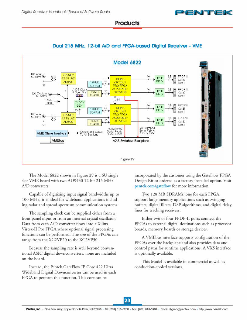
32-32-32-32-32-Channel Narrowband Digital RChannel Narrowband Digital RChannel Narrowband Digital RChannel Narrowband Digital RChannel Narrowband Digital Receiver with FPDP and FPGA - VIM-4eceiver with FPDP and FPGA - VIM-4eceiver with FPDP and FPGA - VIM-4eceiver with FPDP and FPGA - VIM-4eceiver with FPDP and FPGA - VIM-4
The Model 6232 is the digital input counterpart ofthe Model 6230. Instead of four A/D converters, theModel 6232 features two FPDP (Front Panel Data Port)input connectors. FPDP is an industry standard inter-connection scheme for transferring 32-bit digital databetween two devices using flat ribbon cable. Clock ratesup to 40 MHz are supported. FPDP II, the secondgeneration of FPDP, achieves rates up to 100 MHz.
Each 32-bit FPDP port is divided into two 16-bitfields so that two digitized input signals can be broughtin over each port at sampling rates up to 40 MHz.
All four 16-bit digital input words are connected tothe inputs of eight GC4016 quad narrowband digitalreceivers, so that each receiver channel can independentlyselect its source from any one of the four A/D converters.Like the 6230, each receiver channel can be independently
tuned and custom filter coefficients can be downloadedto each channel’s FIR filter.
Again, using an architecture similar to the Model6230, the narrowband receiver outputs and the wide-band FPDP digital inputs are delivered into two XilinxVirtex-E FPGAs in sizes ranging from 300k to 600kgate densities. Again, factory default features of theFPGA include the VIM interface, digital receiver bypass(direct FPDP data into the VIM interface) modes,narrowband channel selection, and various packingmodes. An optional FPGA development kit allowscustom algorithms to be implemented.
Other features include two clock deskewing FIFO’sat the FPDP inputs to realign data coming from twosources with variable delay characteristics.
PPPPProductsroductsroductsroductsroducts
Figure 34
Model 6232Model 6232Model 6232Model 6232Model 6232

PPPPPentek, Inc.entek, Inc.entek, Inc.entek, Inc.entek, Inc. • One Park Way, Upper Saddle River, NJ 07458 • Tel: (201) 818-5900 • Fax: (201) 818-5904 • Email: [email protected] • http://www.pentek.com
2929292929
Digital Receiver Handbook: Basics of Software Radio
The Model 6235 Dual Channel Wideband Receiverin Figure 35 is primarily intended for digitizingwideband IF input signals. Each RF input is transformer-coupled to the A/D converter to support input signals upto 150 MHz for undersampling applications.
Two AD9432 A/D converters digitize the RF inputsto 12-bit samples. The sampling clock is derived froman internal 100 MHz crystal oscillator, an external frontpanel reference input or from an LVDS front panelribbon cable clock and sync board that can be used tosynchronize multiple 6235s. As many as 80 Model6235’s can be synchronized with Pentek’s Model 9190Clock and Sync Generator to support systems withmany channels.
The A/D digital outputs feed two TI/GraychipGC1012B wideband receivers, capable of accepting dataat the 100 MHz rate. These chips can be set for decima-tion values to support output bandwidths from 1.25 MHzto 40 MHz.
Both A/D outputs and both wideband receiveroutputs are delivered into a Xilinx Virtex-II Series FPGA.Here, factory default logic allows channel selection,triggering, receiver bypass, and data packing modes.
FPGA densities range from 1 to 3 million gates(XC2V1000 or 3000) and an optional GateFlow FPGADesign Kit is available to support user-defined customalgorithms.
See the Model 6236 on the next page for GateFlowFPGA IP Core options also available on the 6235.
Dual Channel A/D and WDual Channel A/D and WDual Channel A/D and WDual Channel A/D and WDual Channel A/D and Wideband Rideband Rideband Rideband Rideband Receiver with FPGA - VIM-2eceiver with FPGA - VIM-2eceiver with FPGA - VIM-2eceiver with FPGA - VIM-2eceiver with FPGA - VIM-2
PPPPProductsroductsroductsroductsroducts
Figure 35
Model 6235Model 6235Model 6235Model 6235Model 6235

PPPPPentek, Inc.entek, Inc.entek, Inc.entek, Inc.entek, Inc. • One Park Way, Upper Saddle River, NJ 07458 • Tel: (201) 818-5900 • Fax: (201) 818-5904 • Email: [email protected] • http://www.pentek.com
3030303030
Digital Receiver Handbook: Basics of Software Radio
Dual Channel A/D and WDual Channel A/D and WDual Channel A/D and WDual Channel A/D and WDual Channel A/D and Wideband Rideband Rideband Rideband Rideband Receiver with FPGA - VIM-2eceiver with FPGA - VIM-2eceiver with FPGA - VIM-2eceiver with FPGA - VIM-2eceiver with FPGA - VIM-2
The Model 6236 is identical to the popular 6235but incorporates two new 105 MHz 14-bit A/D Con-verters (Analog Devices AD6645-105). These convertersoffer two additional bits of resolution for improvedaccuracy and dynamic range over the 6235.
In addition to the GateFlow FPGA Design Kit,Pentek offers several popular GateFlow IP Cores asfactory installed options for both the Model 6235 andModel 6236.
For applications requiring FFTs, two different installedFFT cores are available for either 1k- or 4k-point blocksizes (Cores 401 and 404). A complete radar pulsecompression core has also been developed specially forthe 6235 and 6236 (Core 440).
Because the TI/GC1012B wideband digital receiversaccept only 12-bit inputs, two of the A/D converter bitsremain unused.
To take advantage of the additional A/D resolution,Pentek’s GateFlow Wideband Digital Receiver IP Core421 can be factory installed in the FPGA, supporting afull 16-bit input, improved dynamic range, and user-configurable FIR filter coefficients. For this reason, theGC1012B chips are offered as an option to save cost.
See page 10 for more information on factoryinstalled IP Cores and visit the GateFlow Resourceswebsite for all the latest information: pentek.com/gateflow.
PPPPProductsroductsroductsroductsroducts
Figure 36
Model 6236Model 6236Model 6236Model 6236Model 6236

PPPPPentek, Inc.entek, Inc.entek, Inc.entek, Inc.entek, Inc. • One Park Way, Upper Saddle River, NJ 07458 • Tel: (201) 818-5900 • Fax: (201) 818-5904 • Email: [email protected] • http://www.pentek.com
3131313131
Digital Receiver Handbook: Basics of Software Radio
Multiband Digital RMultiband Digital RMultiband Digital RMultiband Digital RMultiband Digital Receivers with A/Ds and FPGAseceivers with A/Ds and FPGAseceivers with A/Ds and FPGAseceivers with A/Ds and FPGAseceivers with A/Ds and FPGAs
support the receiver bypass path to the PCI bus and fordirect processing of the wideband A/D signals by the FPGA.
The unit supports the channel combining mode ofthe 4016s such that two or four individual 2.5 MHzchannels can be combined for output bandwidths of5 MHz or 10 MHz, respectively.
The sampling clock can be sourced from an internal100 MHz crystal oscillator or from an external clock suppliedthrough an SMA connector or the LVDS clock/sync bus onthe front panel. The LVDS bus allows multiple modules to besynchronized with the same sample clock, gating, triggeringand frequency switching signals. Up to 80 modules can besynchronized with the Model 9190 Clock and Sync Genera-tor. Custom interfaces can be implemented by using the 64user-defined FPGA I/O pins on the P4 connector.
The FPGA is fully supported with the GateFlowFPGA Design Kit and GateFlow FPGA IP CoreLibrary. Software drivers support VxWorks, Windowsand Linux processor board operating systems.
PPPPProductsroductsroductsroductsroducts
The Model 7131, a 16-Channel Multiband Receiver,is a PMC module. The 7131 PMC may be attached to awide range of industry processor platforms equippedwith PMC sites. The faceplate of a PMC module fits ina cutout on the front panel of the processor board andthe PCI bus interface to the processor board is madethrough connectors at the rear of the module.
Versions of the 7131 are also available as PCIboards (7631) and 6U or 3U CompactPCI boards(7231 or 7331). All three products have similar features.
Two 14-bit 105 MHz A/D Converters (Analog DevicesAD6645) accept transformer-coupled RF inputs throughtwo front panel SMA connectors. Both inputs are connectedto four TI/GC4016 quad digital receiver chips, so that all 16receiver channels can independently select either A/D.
Four parallel outputs from the four receivers deliverdata into the Virtex-II FPGA which can be either theXC2V1000 or XC2V3000. The outputs of the two A/Dconverters are also connected directly to the FPGA to
Model 7131 PMC Model 7131 PMC Model 7131 PMC Model 7131 PMC Model 7131 PMC ●●●●● Model 7631 PCI Model 7631 PCI Model 7631 PCI Model 7631 PCI Model 7631 PCI ●●●●● Model 7231 6U cPCI Model 7231 6U cPCI Model 7231 6U cPCI Model 7231 6U cPCI Model 7231 6U cPCI ●●●●● Model 7331 3U cPCI Model 7331 3U cPCI Model 7331 3U cPCI Model 7331 3U cPCI Model 7331 3U cPCI
Model 7131PMC
Figure 37
Model 7631PCI
Model 72316U cPCI
Model 73313U cPCI
PPPPPentek, Inc.entek, Inc.entek, Inc.entek, Inc.entek, Inc. • One Park Way, Upper Saddle River, NJ 07458 • Tel: (201) 818-5900 • Fax: (201) 818-5904 • Email: [email protected] • http://www.pentek.com
3232323232
Digital Receiver Handbook: Basics of Software Radio
Dual FPDP Adapter with VirDual FPDP Adapter with VirDual FPDP Adapter with VirDual FPDP Adapter with VirDual FPDP Adapter with Virtex-II FPGAs - VIM-2tex-II FPGAs - VIM-2tex-II FPGAs - VIM-2tex-II FPGAs - VIM-2tex-II FPGAs - VIM-2
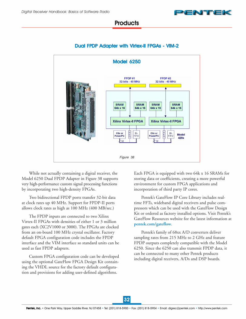
While not actually containing a digital receiver, theModel 6250 Dual FPDP Adapter in Figure 38 supportsvery high-performance custom signal processing functionsby incorporating two high-density FPGAs.
Two bidirectional FPDP ports transfer 32-bit dataat clock rates up 40 MHz. Support for FPDP-II portsallows clock rates as high as 100 MHz (400 MB/sec.)
The FPDP inputs are connected to two XilinxVirtex-II FPGAs with densities of either 1 or 3 milliongates each (XC2V1000 or 3000). The FPGAs are clockedfrom an on-board 100 MHz crystal oscillator. Factorydefault FPGA configuration code includes the FPDPinterface and the VIM interface so standard units can beused as fast FPDP adapters.
Custom FPGA configuration code can be developedusing the optional GateFlow FPGA Design Kit contain-ing the VHDL source for the factory default configura-tion and provisions for adding user-defined algorithms.
Each FPGA is equipped with two 64k x 16 SRAMs forstoring data or coefficients, creating a more powerfulenvironment for custom FPGA applications andincorporation of third party IP cores.
Pentek’s GateFlow IP Core Library includes real-time FFTs, wideband digital receivers and pulse com-pressors which can be used with the GateFlow DesignKit or ordered as factory installed options. Visit Pentek’sGateFlow Resources website for the latest information atpentek.com/gateflow.
Pentek’s family of 68xx A/D converters deliversampling rates from 215 MHz to 2 GHz and featureFPDP outputs completely compatible with the Model6250. Since the 6250 can also transmit FPDP data, itcan be connected to many other Pentek productsincluding digital receivers, A/Ds and DSP boards.
PPPPProductsroductsroductsroductsroducts
Figure 38
Model 6250Model 6250Model 6250Model 6250Model 6250

PPPPPentek, Inc.entek, Inc.entek, Inc.entek, Inc.entek, Inc. • One Park Way, Upper Saddle River, NJ 07458 • Tel: (201) 818-5900 • Fax: (201) 818-5904 • Email: [email protected] • http://www.pentek.com
3333333333
Digital Receiver Handbook: Basics of Software Radio
Dual FPDP Adapter with VirDual FPDP Adapter with VirDual FPDP Adapter with VirDual FPDP Adapter with VirDual FPDP Adapter with Virtex-II Ptex-II Ptex-II Ptex-II Ptex-II Pro FPGAs and SDRAM - VIM-2ro FPGAs and SDRAM - VIM-2ro FPGAs and SDRAM - VIM-2ro FPGAs and SDRAM - VIM-2ro FPGAs and SDRAM - VIM-2
A GateFlow FPGA Design Kit is available forcustom algorithm development. It includes all theVHDL source code for the standard factory functionsand library functions to support the SDRAM memory.
When used in conjunction with FPDP data sourceslike Pentek’s Series 68xx A/D Converters, the 6251 offerssignificant signal processing horsepower.
Pentek’s GateFlow Wideband Digital Receiver IPCores 421 and 422 can be used to provide high-speedand high-dynamic range digital downconversion.GateFlow FFT IP Cores 401 and 404 deliver world-class,real-time time-to-frequency domain conversion. TheGateFlow Pulse Compression IP Core 440 handles real-time radar pulse compression with block-floating pointprecision. Visit the GateFlow Resources website atpentek.com/gateflow.
The Model 6251 is the next generation successor tothe popular 6250 shown on the previous page.
Major new features of 6251 are two Virtex-II ProFPGAs that replace the Virtex-II devices with twice theresources plus two embedded PowerPC microcontrollers.
In addition, the four 128 kB SRAMs on the 6250have been replaced with 64 MByte SDRAMs on the6251, increasing the memory capacity of the module bya factor of 256.
These larger memories can now support long digitaldelay lines and large data buffers for transient captureapplications. The 16 MB FLASH memories can be usedfor coefficient or boot code storage for the embeddedmicrocontrollers.
The FPGA sizes range from the XC2VP20 to theXC2VP50 to handle a wide range of applications.
PPPPProductsroductsroductsroductsroducts
Figure 39
Model 6251Model 6251Model 6251Model 6251Model 6251

PPPPPentek, Inc.entek, Inc.entek, Inc.entek, Inc.entek, Inc. • One Park Way, Upper Saddle River, NJ 07458 • Tel: (201) 818-5900 • Fax: (201) 818-5904 • Email: [email protected] • http://www.pentek.com
3434343434
Digital Receiver Handbook: Basics of Software Radio
Dual Channel WDual Channel WDual Channel WDual Channel WDual Channel Wideband Digital Upconverideband Digital Upconverideband Digital Upconverideband Digital Upconverideband Digital Upconverter and D/A - VIM-2ter and D/A - VIM-2ter and D/A - VIM-2ter and D/A - VIM-2ter and D/A - VIM-2
The Model 6229 Dual Channel Wideband DigitalUpconverter in Figure 40 complements the digitalreceiver products by offering an analogous transmit sidefunction.
The Model 6229 employs two AD9856 digitalupconverters containing several stages of signal processingwithin a single monolithic device. The VIM-2 processordelivers complex (I & Q) digital baseband signals at datarates from audio up to 25 Msamples/sec.
The AD9856 uses an interpolation filter to upsamplethese inputs to a sampling rate of 200 MHz. The signalsare then translated in frequency using quadrature mixerswith programmable local oscillators.
This single-sideband frequency translation allowsthe baseband signal to be placed anywhere between DCand 80 MHz, suitable for many IF inputs for transmit-ters or exciters.
Finally, the translated signals are converted toanalog by 12-bit 200 MHz D/A converters and deliv-ered to front panel SMA connectors though the outputamplifier stages.
The Model 6229 is ideal for developers of newwireless standards, for testing receiver systems and as ageneral purpose arbitrary waveform generator. The localoscillator can also be used as a CW sinewave oscillatorwith outputs programmable from DC to 80 MHz.
PPPPProductsroductsroductsroductsroducts
Figure 40
Model 6229Model 6229Model 6229Model 6229Model 6229

PPPPPentek, Inc.entek, Inc.entek, Inc.entek, Inc.entek, Inc. • One Park Way, Upper Saddle River, NJ 07458 • Tel: (201) 818-5900 • Fax: (201) 818-5904 • Email: [email protected] • http://www.pentek.com
3535353535
Digital Receiver Handbook: Basics of Software Radio
Dual Channel WDual Channel WDual Channel WDual Channel WDual Channel Wideband Digital Upconverideband Digital Upconverideband Digital Upconverideband Digital Upconverideband Digital Upconverter and D/A - VIM-2ter and D/A - VIM-2ter and D/A - VIM-2ter and D/A - VIM-2ter and D/A - VIM-2
The Model 6228 Dual Channel Wideband DigitalUpconverter in Figure 41 is the next generation versionof the Model 6229.
It uses two Texas Instruments DAC5686 digitalupconverter chips that include an interpolation filter, alocal oscillator, a complex mixer and two 16-bit D/Aconverters.
When operated as a digital upconverter, the maxi-mum clock rate is 320 MHz. This allows digital base-band complex input sampling rates up to 80 MHz andoutput IF frequencies tunable up to 160 MHz.
For the real IF output mode, only one of the 16-bitD/A converters of each DAC5686 is used. For thecomplex output mode, both D/A converters are used todeliver both I and Q analog signals.
When operated in the D/A only mode, the frequencytranslation functions are not used. In this mode, themaximum clock frequency for the interpolation filterand D/A converters becomes 500 MHz. With twoupconverter chips in the module, four independent datastreams can be delivered to the four 16-bit D/A convert-ers, with optional interpolation for generation of signalbandwidths as high as 200 MHz.
The Virtex-II FPGA can be used as a preprocessorfront end for the upconverters to implement additionalinterpolation filtering or other custom signal processingfunctions. An arbitrary waveform generator could beconstructed using internal FPGA memory for waveformstorage. A complete GateFlow FPGA Design Kit isavailable.
PPPPProductsroductsroductsroductsroducts
Figure 41
Model 6228Model 6228Model 6228Model 6228Model 6228

PPPPPentek, Inc.entek, Inc.entek, Inc.entek, Inc.entek, Inc. • One Park Way, Upper Saddle River, NJ 07458 • Tel: (201) 818-5900 • Fax: (201) 818-5904 • Email: [email protected] • http://www.pentek.com
3636363636
Digital Receiver Handbook: Basics of Software Radio
Digital UpconverDigital UpconverDigital UpconverDigital UpconverDigital Upconverters / Downconverters / Downconverters / Downconverters / Downconverters / Downconverterstersterstersters
PPPPProductsroductsroductsroductsroducts
Figure 42
Model 7140 PMC/XMC Model 7140 PMC/XMC Model 7140 PMC/XMC Model 7140 PMC/XMC Model 7140 PMC/XMC ●●●●● Model 7640 PCI Model 7640 PCI Model 7640 PCI Model 7640 PCI Model 7640 PCI ●●●●● Model 7240 6U cPCI Model 7240 6U cPCI Model 7240 6U cPCI Model 7240 6U cPCI Model 7240 6U cPCI ●●●●● Model 7340 3U cPCI Model 7340 3U cPCI Model 7340 3U cPCI Model 7340 3U cPCI Model 7340 3U cPCI
Model 7140PMC/XMC
The Model 7140 PMC module combines bothtransmit and receive capability with a high-performanceVirtex II-Pro FPGA and supports the emerging VITA42 XMC standard with optional switched fabric inter-faces for high-speed I/O.
The front end of the module accepts two +4 dBm full-scale analog RF inputs and transformer couples them intotwo 14-bit A/D converters running at 105 MHz. Thedigitized output signals pass to a Virtex-II Pro FPGAfor signal processing or routing to other moduleresources.
These resources include a quad digitaldownconverter, a digital upconverter with dual D/Aconverters, 512 MB DDR SDRAM delay memory andthe PCI bus. The FPGA also serves as a control andstatus engine with data and programming interfaces to
each of the on-board resources. Factory-installed FPGAfunctions include data multiplexing, channel selection, datapacking, gating, triggering, and SDRAM memory control.
Because the FPGA controls the data flow within themodule as well as providing signal processing, the modulecan be configured for many different functions. Inaddition to acting as a simple transceiver, the modulecan perform user-defined DSP functions on the base-band signals, developed using Pentek’s GateFlow andReadyFlow® development tools.
The module includes a TI/GC4016 quad digitaldownconverter along with a TI DAC5686 digitalupconverter with dual D/A converters.
Each channel in the downconverter can be set with anindependent tuning frequency and bandwidth. ➤

PPPPPentek, Inc.entek, Inc.entek, Inc.entek, Inc.entek, Inc. • One Park Way, Upper Saddle River, NJ 07458 • Tel: (201) 818-5900 • Fax: (201) 818-5904 • Email: [email protected] • http://www.pentek.com
3737373737
Digital Receiver Handbook: Basics of Software Radio
Digital UpconverDigital UpconverDigital UpconverDigital UpconverDigital Upconverters / Downconverters / Downconverters / Downconverters / Downconverters / Downconverterstersterstersters
PPPPProductsroductsroductsroductsroducts
The upconverter translates a real or complex basebandsignal to any IF center frequency from DC to 160 MHzand can deliver real or complex (I + Q) analog outputsthrough its two 16-bit D/A converters. The digitalupconverter can be bypassed for two interpolated D/Aoutputs with sampling rates to 500 MHz.
Inputs to the downconverter can come from manysources, including the input A/D converters, the FPGAsignal processing engines, the SDRAM delay memory,or data sources on the PCI bus. The built-in clock/syncbus supports multiple module synchronization as well asdual on-board oscillators for independent input andoutput clock rates. Furthermore, the Model 7140 offersthe VITA 42 XMC interface. This allows it to transferdata through optional Serial RapidIO, PCI-Express, orother switched fabric interfaces, which provide a high-speed streaming data path that is independent of thePCI bus.
A clock/sync bus allows synchronization of localoscillator phase, frequency switching, decimating filterphase and data collection among multiple 7140s. Oneboard acts as a master, driving clock, sync and gatesignals out to a front panel flat cable bus using LVDSdifferential signaling. The master alone can drive asmany as seven slaves. By using a Pentek Model 9190Clock and Sync Generator to drive the signals, as manyas 80 modules can be configured to operate synchronously.
For more information on the Model 7140 SoftwareRadio Transceiver, visit pentek.com/sftradcentral.
As shown in Figure 43, this module is also availablein a variety of form factors including PCI (Model 7640),3U cPCI (Model 7340), 6U cPCI (Model 7240 with twicethe density of the other models) and a PMC conduction-cooled version (Model 7140-700). These models are alsoavailable with IP Core 430, a 256-channel narrowbandreceiver, installed, see the next page for more information.
Model 7140 PMC/XMC Model 7140 PMC/XMC Model 7140 PMC/XMC Model 7140 PMC/XMC Model 7140 PMC/XMC ●●●●● Model 7640 PCI Model 7640 PCI Model 7640 PCI Model 7640 PCI Model 7640 PCI ●●●●● Model 7240 6U cPCI Model 7240 6U cPCI Model 7240 6U cPCI Model 7240 6U cPCI Model 7240 6U cPCI ●●●●● Model 7340 3U cPCI Model 7340 3U cPCI Model 7340 3U cPCI Model 7340 3U cPCI Model 7340 3U cPCI
Model 7640PCI
Model 72406U cPCI
Model 73403U PCI
Figure 43
➤

PPPPPentek, Inc.entek, Inc.entek, Inc.entek, Inc.entek, Inc. • One Park Way, Upper Saddle River, NJ 07458 • Tel: (201) 818-5900 • Fax: (201) 818-5904 • Email: [email protected] • http://www.pentek.com
3838383838
Digital Receiver Handbook: Basics of Software Radio
TTTTTransceiver with 256-ransceiver with 256-ransceiver with 256-ransceiver with 256-ransceiver with 256-Channel Narrowband DDC Installed CoreChannel Narrowband DDC Installed CoreChannel Narrowband DDC Installed CoreChannel Narrowband DDC Installed CoreChannel Narrowband DDC Installed Core
PPPPProductsroductsroductsroductsroducts
Model 7140Model 7140Model 7140Model 7140Model 7140-430-430-430-430-430
Figure 44
CH ARF In
SampleClock A In
CLOCK &SYNC
GENERATOR
AD6645105 MHz
14-bit A/D
GC4016 DIGITALDOWNCONVERTER
XILINX XC2VP50 FPGA WITH GATEFLOW FACTORY INSTALLED CORE 430
XTALOSC A
RFXFORMR
CH BRF In
AD6645105 MHz
14-bit A/D
RFXFORMR
D
SampleClock B In
CH ARF Out
16-BIT500 MHz
D/A
RFXFORMR
CH BRF Out
16-BIT500 MHz
D/A
RFXFORMR
DAC5686DIGITAL
UPCONVERTER
PCI 2.2INTERFACE
PCI BUS64 bits/66 MHzClock/Sync
Bus
XTALOSC B
CBA
DCBA
A/D AFIFO
A/D BFIFO
DDC AFIFO
DDC BFIFO
DDC CFIFO
DDC DFIFO
D/A AFIFO
D/A BFIFO
MUX
OUT ADDC A
OUT BDDC B
OUT CDDC C
OUT DDDC D
CHANNELIZATION
CHANNELSWITCHMATRIX
CHAN 1 1
CHAN 1024
TUNINGCONTROL
COARSE TUNING
FINE TUNING
FIRCOMPENSATION
FILTER
OUTPUTGAIN
2 FIRCOMPENSATION
FILTER
OUTPUTGAIN
255 FIRCOMPENSATION
FILTER
OUTPUTGAIN
256 FIRCOMPENSATION
FILTER
OUTPUTGAIN
CHAN 2
CHAN 3
CHAN 1023
CHAN 1022
MUX
DDC1
DDC2
DDC255
DDC256
MUXA/D A
A/D BMUX
For applications that require many channels ofnarrowband downconverters, Pentek offers the GateFlowIP Core 430 256-channel digital downconverter bank.Factory installed in the Model 7140 FPGA as shown inFigure 44, Core 430 creates a flexible, very high channelcount receiver system in a small footprint.
Unlike classic channelizer methods, the Pentek 430core allows for completely independent programmabletuning of each individual channel with 32-bit resolutionas well as filter characteristics comparable to manyconventional ASIC DDCs.
Added flexibility comes from programmable globaldecimation settings ranging from 1024 to 8192 in stepsof 256, and 18-bit user programmable FIR decimatingfilter coefficients for the DDCs. Default DDC filtercoefficient sets are included with the core for all possibledecimation settings.
Core 430 utilizes a unique method of channelization.It differs from others in that the channel center frequen-cies need not be at fixed intervals, and are independentlyprogrammable to any value.
Core 430 DDC comes factory installed in theModel 7140-430. A multiplexer in front of the coreallows data to be sourced from either A/D converter Aor B. At the output, a multiplexer allows the 7140 toroute either the output of the GC4016 or the Core 430DDC to the PCI Bus.
In addition to the DDC outputs, data from bothA/D channels are presented to the PCI Bus at a rateequal to the A/D clock rate divided by any intergervalue between 1 and 4096. A TI DAC5686 digitalupconverter and dual D/A accepts baseband real or complexdata streams from the PCI Bus with signal bandwidths upto 40 MHz.
Core 430 is also available for the Models 7240,7340 and 7640.

PPPPPentek, Inc.entek, Inc.entek, Inc.entek, Inc.entek, Inc. • One Park Way, Upper Saddle River, NJ 07458 • Tel: (201) 818-5900 • Fax: (201) 818-5904 • Email: [email protected] • http://www.pentek.com
3939393939
Digital Receiver Handbook: Basics of Software Radio
SystemsSystemsSystemsSystemsSystems
RRRRReal-eal-eal-eal-eal-Time WTime WTime WTime WTime Wideband Signal Pideband Signal Pideband Signal Pideband Signal Pideband Signal Processing Systemrocessing Systemrocessing Systemrocessing Systemrocessing System
The Pentek RTS 2501 in Figure 45 is one of severalhighly-scalable, real-time platforms for acquiring, down-converting, processing, and recording wideband signals.
The heart of the RTS 2501 is the Pentek Model4205 I/O Processor featuring a 1 GHz MPC7457G4 PowerPC, mezzanine sites for both VIM and PMCmodules, and two Xilinx Virtex-II FPGAs. The G4PowerPC acts both as an executive for managing datatransfer tasks as well as performing digital signal process-ing or formatting functions.
Attached to the 4205 I/O Processor are two Model6236 Dual Channel A/D and Wideband Receiver VIMmodules, each with two 14-bit 105 MHz A/D convert-ers, two TI/GC1012B wideband digital downconvertersand a Virtex-II FPGA.
A built-in Fibre Channel interface connects directlyto JBOD or RAID hard disks for real time storage atrates up to 100 MB/sec. Optional RACE++ interfacesprovide excellent I/O connectivity without sacrificingany of the mezzanine sites. Standard RS-232 and 100base T Ethernet ports allow the PowerPC to communi-cate with a wide range of host workstations for controland software development applications.
Scalable from 2 to 80 channels in a single 6UVMEbus chassis, the RTS 2501 serves equally well as adevelopment platform for advanced research projectsand proof-of-concept prototypes, or as a cost-effectivestrategy for deploying high-performance, multichannelembedded systems.
More information on RTS systems on pentek.com.
Model RTS 2501 Model RTS 2501 Model RTS 2501 Model RTS 2501 Model RTS 2501
Figure 45

PPPPPentek, Inc.entek, Inc.entek, Inc.entek, Inc.entek, Inc. • One Park Way, Upper Saddle River, NJ 07458 • Tel: (201) 818-5900 • Fax: (201) 818-5904 • Email: [email protected] • http://www.pentek.com
4040404040
Digital Receiver Handbook: Basics of Software Radio
SystemsSystemsSystemsSystemsSystems
RRRRReal-eal-eal-eal-eal-Time WTime WTime WTime WTime Wideband Signal Pideband Signal Pideband Signal Pideband Signal Pideband Signal Processing and Rrocessing and Rrocessing and Rrocessing and Rrocessing and Recording Systemecording Systemecording Systemecording Systemecording System
The Pentek RTS 2502 in Figure 46 is also a highly-scalable, real-time platforms for acquiring, downconverting,processing, and recording wideband signals.
The heart of the RTS 2502 is the Pentek Model4205 I/O Processor featuring a 1 GHz MPC7457G4 PowerPC, mezzanine sites for both VIM and PMCmodules, and two Xilinx Virtex-II FPGAs. The G4PowerPC acts both as an executive for managing datatransfer tasks as well as performing digital signal process-ing or formatting functions.
Attached to the 4205 I/O Processor is a Model6236 Dual Channel A/D and Wideband Receiver VIMmodule with two 14-bit 105 MHz A/D converters, twoTI/GC1012B wideband digital downconverters and aVirtex-II FPGA.
Also attached to the 4205 processor is a Model6228 4-channel 16-bit 500 MHz D/A with digitalupconverters and a Virtex-II FPGA. The 6228 providesa path for analog playback of recorded signals or forreal-time transmission of signals received by the 6236.
A built-in Fibre Channel interface connects directlyto JBOD or RAID hard disks for real time storage atrates up to 100 MB/sec. Optional RACE++ interfacesprovide excellent I/O connectivity without sacrificingany of the mezzanine sites. Standard RS-232 and 100base T Ethernet ports allow the PowerPC to communi-cate with a wide range of host workstations for controland software development applications.
More information on RTS systems on pentek.com.
Model RTS 2502 Model RTS 2502 Model RTS 2502 Model RTS 2502 Model RTS 2502
Figure 46

PPPPPentek, Inc.entek, Inc.entek, Inc.entek, Inc.entek, Inc. • One Park Way, Upper Saddle River, NJ 07458 • Tel: (201) 818-5900 • Fax: (201) 818-5904 • Email: [email protected] • http://www.pentek.com
4141414141
Digital Receiver Handbook: Basics of Software Radio
SystemsSystemsSystemsSystemsSystems
RRRRReal-eal-eal-eal-eal-Time WTime WTime WTime WTime Wideband Signal Pideband Signal Pideband Signal Pideband Signal Pideband Signal Processing Systemrocessing Systemrocessing Systemrocessing Systemrocessing System
The Pentek RTS 2503 in Figure 47 extends therange of highly-scalable, real-time platforms for acquiring,downconverting, processing, and recording widebandsignals to 215 MHz sampling frequency, by utilizing thesingle-channel Model 6821 or the dual channel Model6822 215 MHz, 12-bit A/D converters. These attach tothe Model 4205 I/O Processor with two Pentek Model6226 FPDP Adapter VIM-2 modules. This systemoccupies two VMEbus slots.
Again, the heart of the RTS 2503 is the PentekModel 4205 I/O Processor featuring a 1 GHzMPC7457 G4 PowerPC, mezzanine sites for both VIMand PMC modules, and two Xilinx Virtex-II FPGAs.The G4 PowerPC acts both as an executive for managingdata transfer tasks as well as performing digital signalprocessing or formatting functions.
The built-in Fibre Channel interface connectsdirectly to JBOD or RAID hard disks for real timestorage at rates up to 100 MB/sec. Optional RACE++interfaces provide excellent I/O connectivity withoutsacrificing any of the mezzanine sites. Standard RS-232and 100 base T Ethernet ports allow the PowerPC tocommunicate with a wide range of host workstations forcontrol and software development applications.
Scalable from 1 to 20 channels in a single 6UVMEbus chassis, the RTS 2503 allows the designengineer to take advantage of the latest technology forresearch projects and proof-of-concept prototypes, or asa cost-effective strategy for deploying high-performance,multichannel embedded systems.
More information on RTS systems on pentek.com.
Model RTS 2503 Model RTS 2503 Model RTS 2503 Model RTS 2503 Model RTS 2503
Figure 47

PPPPPentek, Inc.entek, Inc.entek, Inc.entek, Inc.entek, Inc. • One Park Way, Upper Saddle River, NJ 07458 • Tel: (201) 818-5900 • Fax: (201) 818-5904 • Email: [email protected] • http://www.pentek.com
4242424242
Digital Receiver Handbook: Basics of Software Radio
SystemsSystemsSystemsSystemsSystems
RRRRReal-eal-eal-eal-eal-Time WTime WTime WTime WTime Wideband Signal Pideband Signal Pideband Signal Pideband Signal Pideband Signal Processing and Rrocessing and Rrocessing and Rrocessing and Rrocessing and Recording Systemecording Systemecording Systemecording Systemecording System
The Pentek RTS 2504 in Figure 48 is similar to theSystem RTS 2502, except that the Models 6236 and6228 have been replaced by the Model 7140 TransceiverPMC module described on page 36. The Model 7140combines the downconverters and upconverters of thesetwo models in one PMC/XMC module. Except for thischange, the system performance and characteristics areidentical.
Again, the heart of the RTS 2504 is the PentekModel 4205 I/O Processor featuring a 1 GHzMPC7457 G4 PowerPC, mezzanine sites for both VIMand PMC modules, and two Xilinx Virtex-II FPGAs.The G4 PowerPC acts both as an executive for manag-ing data transfer tasks as well as performing digital signalprocessing or formatting functions.
A built-in Fibre Channel interface connects directlyto JBOD or RAID hard disks for real time storage atrates up to 100 MB/sec. Optional RACE++ interfacesprovide excellent I/O connectivity without sacrificingany of the mezzanine sites. Standard RS-232 and 100base T Ethernet ports allow the PowerPC to communi-cate with a wide range of host workstations for controland software development applications.
Scalable from 1 to 40 channels in a single 6UVMEbus chassis, the RTS 2504 serves equally well as adevelopment platform for advanced research projectsand proof-of-concept prototypes, or as a cost-effectivestrategy for deploying high-performance, multichannelembedded systems.
More information on RTS systems on pentek.com.
Model RTS 2504 Model RTS 2504 Model RTS 2504 Model RTS 2504 Model RTS 2504
Figure 48

PPPPPentek, Inc.entek, Inc.entek, Inc.entek, Inc.entek, Inc. • One Park Way, Upper Saddle River, NJ 07458 • Tel: (201) 818-5900 • Fax: (201) 818-5904 • Email: [email protected] • http://www.pentek.com
4343434343
Digital Receiver Handbook: Basics of Software Radio
SystemsSystemsSystemsSystemsSystems
SCASCASCASCASCA-----Compliant SofCompliant SofCompliant SofCompliant SofCompliant Software Defined Rtware Defined Rtware Defined Rtware Defined Rtware Defined Radio Development Systemadio Development Systemadio Development Systemadio Development Systemadio Development System
The Pentek SCA 2510 Development Platformshown in Figure 49, is a complete low-cost system fordeveloping software defined radio products.
The 7640 transceiver PCI board that we discussedon pages 36 and 37, ported with all the necessary SCAinfrastructure, creates an SCA-compliant platform.Comprised of hardware and software componentscompatible with the SCA standard, the SCA 2510platform is a PC-based system that runs under Linux.
The system includes an installed CRC SCARI++core framework, Component Development Library andSDR development tools, plus the Pentek SCA boardsupport package for the model 7640 and all the board-specific components.
This complete platform satisfies SCA requirementsby offering a low-cost solution suitable for waveformdevelopers, application developers and system integrators.
To support scalability to large platforms, an additional7640 PCI card can be installed right in the PC mother-board. Furthermore, the identical board architecture isavailable in a PMC form factor, or a 3U or a 6U Comp-actPCI form factor that can be convection-cooled, rugge-dized, or conduction-cooled.
These are all extremely appropriate for large deployedmultichannel military systems. Future SCA systemdevelopment based on these additional form factors isplanned.
Model SCA 2510 Model SCA 2510 Model SCA 2510 Model SCA 2510 Model SCA 2510
Figure 49

PPPPPentek, Inc.entek, Inc.entek, Inc.entek, Inc.entek, Inc. • One Park Way, Upper Saddle River, NJ 07458 • Tel: (201) 818-5900 • Fax: (201) 818-5904 • Email: [email protected] • http://www.pentek.com
4444444444
Digital Receiver Handbook: Basics of Software Radio
• Reduction of DSP processing demands
• Very fast tuning - No PLL’S
• Fast bandwidth selection
• Zero frequency drift and error
• Precise, stable filter characteristics
• Excellent dynamic range
SummarSummarSummarSummarSummaryyyyy
Benefits of Digital Receivers:
To summarize, we first restate the major benefit ofdigital receivers:
Digital receivers can dramatically reduce the DSPrequirements for systems which need to process signals con-tained within a certain frequency band of a wideband signal.
The fast tuning of the digital local oscillator and theeasy bandwidth selection in the decimating digital filtermake the digital receiver easy to control.
Since all of the circuitry uses digital signal process-ing, the characteristics are precise, predictable, and willnot drift with time, temperature or aging. This alsomeans excellent channel-to-channel matching and no needfor calibration, alignment or maintenance.
With the addition of FPGA technology, dramaticincreases in system density have been coupled with asignificantly lower cost per channel. Furthermore,FPGA technology allows users to incorporate customalgorithms right at the front end of these systems.
As we have seen, there are inherently many benefitsand advantages to you when using digital receivers. Wehope that this introduction to digital receivers has beeninformative. We stand ready to discuss your requirementsand help you configure a complete digital receiver system.
For all the latest information about Pentek’s digitalreceivers, DSP boards and data acquisition products, besure to visit Pentek’s comprehensive website regularly at:pentek.com.
Pentek offers a comprehensive array of VMEbusDSP boards featuring the TMS320C6000 family ofprocessor products from Texas Instruments and theAltiVec G4 PowerPC from Freescale.
On-board processor densities range from one toeight DSPs with many different memory and interfaceoptions available.
The Model 4290/91/92/93 series of VIM quadprocessor boards features the Texas Instruments latestTMS320C6000 family of fixed and floating point DSPsthat represent a 10-fold increase in processing powerover previous designs.
The Models 4294 and 4295 VIM processor boardsfeature four MPC74xx G4 PowerPC processors utilizingthe AltiVec vector processor capable of delivering severalGFLOPS of processing power.
The Model 4205 G4 PowerPC I/O processor boardaccepts both VIM and PMC mezzanines and includesbuilt-in dual RACE++ interfaces plus Fibre Channel.
Once again, the ability of the system designer tofreely choose the most appropriate DSP processor foreach digital receiver application, facilitates systemrequirement changes and performance upgrades.
Full software development tools are available for work-stations running Windows, Solaris, and Linux with manydifferent development system configurations available.
DSP Boards for VMEbusDSP Boards for VMEbusDSP Boards for VMEbusDSP Boards for VMEbusDSP Boards for VMEbus
PPPPProductsroductsroductsroductsroducts
Figure 50
• Freescale Altivec G4PowerPC
• Texas InstrumentsC6000 DSPs
• Single, Dual, Quad andOctal Processor versions
• PMC, VIM, PCI andcPCI Mezzanines
• RACEway, RACE++,FPDP and Fibre ChannelInterfaces

PPPPPentek, Inc.entek, Inc.entek, Inc.entek, Inc.entek, Inc. • One Park Way, Upper Saddle River, NJ 07458 • Tel: (201) 818-5900 • Fax: (201) 818-5904 • Email: [email protected] • http://www.pentek.com
4545454545
Digital Receiver Handbook: Basics of Software Radio
LinksLinksLinksLinksLinks
The following live links provide you with additional information about the Pentek Productsand Systems presented in this handbook. Just click on the Model number. Live links are also provided to other handbooks or brochures that may be of interest in your software radio development projects.
ModelModelModelModelModel DescriptionDescriptionDescriptionDescriptionDescription PPPPPageageageageage
6228 Dual Channel Wideband Digital Upconverter and D/A - VIM-2 356229 Dual Channel Wideband Digital Upconverter and D/A - VIM-2 346230 32-Channel Narrowband Digital Receiver with A/D and FPGA - VIM-4 276232 32-Channel Narrowband Digital Receiver with A/D and FPGA - VIM-4 286235 Dual Channel A/D and Wideband Receiver with FPGA - VIM-2 296236 Dual Channel A/D and Wideband Receiver with FPGA - VIM-2 306250 Dual FPDP Adapter with Virtex-II FPGAs - VIM-2 326251 Dual FPDP Adapter with Virtex-II Pro FPGAs and SDRAM - VIM-2 336821 215 MHz, 12-bit A/D and FPGA-based Digital Receiver - VME 226822 Dual 215 MHz, 12-bit A/D and FPGA-based Digital Receiver - VME 236823 Quad 500 MHz, 8-bit A/D and FPGA-based Digital Receiver - VME 246826 Dual 2 GHz, 10-bit A/D and FPGA-based Digital Receiver - VME 257131 Multiband Digital Receiver with A/Ds and FPGA - PMC 317140 Digital Upconverter / DownConverter - PMC/XMC 367140-430 Transceiver with 2560 Channel Narrowband DDC Installed Core 387231 Multiband Digital Receiver with A/Ds and FPGA - 6U cPCI 317240 Digital Upconverter / DownConverter - 6U cPCI 367331 Multiband Digital Receiver with A/Ds and FPGA - 3U cPCI 317340 Digital Upconverter / DownConverter - 3U cPCI 367631 Multiband Digital Receiver with A/Ds and FPGA - PCI 317640 Digital Upconverter / DownConverter - PCI 36RTS 2501 Real-Time Wideband Signal Processing System 39RTS 2502 Real-Time Wideband Signal Processing and Recording System 40RTS 2503 Real-Time Wideband Signal Processing System 41RTS 2504 Real-Time Wideband Signal Processing and Recording System 42SCA 2510 SCA-Compliant Software Defined Radio Development System 43
Handbooks & BrochuresHandbooks & BrochuresHandbooks & BrochuresHandbooks & BrochuresHandbooks & Brochures
Click here Putting FPGAs to Work for Software RadioClick here Critical Techniques for High-Speed A/D Converters in Real-Time SystemsClick here High-Speed A/D Boards & Real-Time SystemsClick here Achieving SCA Compliance for COTS Software Defined Radio