Embed Size (px)
Citation preview

DIGITAL LOGIC DESIGNCourse Code: 328356(28)
Mr. Manjeet Singh Sonwani Assistant Professor
Department of Electronics & Telecomm.Government Engineering College Raipur
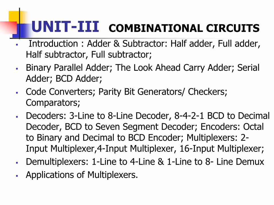
UNIT-III COMBINATIONAL CIRCUITS§ Introduction : Adder & Subtractor: Half adder, Full adder,
Half subtractor, Full subtractor; § Binary Parallel Adder; The Look Ahead Carry Adder; Serial
Adder; BCD Adder; § Code Converters; Parity Bit Generators/ Checkers;
Comparators; § Decoders: 3-Line to 8-Line Decoder, 8-4-2-1 BCD to Decimal
Decoder, BCD to Seven Segment Decoder; Encoders: Octal to Binary and Decimal to BCD Encoder; Multiplexers: 2- Input Multiplexer,4-Input Multiplexer, 16-Input Multiplexer;
§ Demultiplexers: 1-Line to 4-Line & 1-Line to 8- Line Demux § Applications of Multiplexers.
3
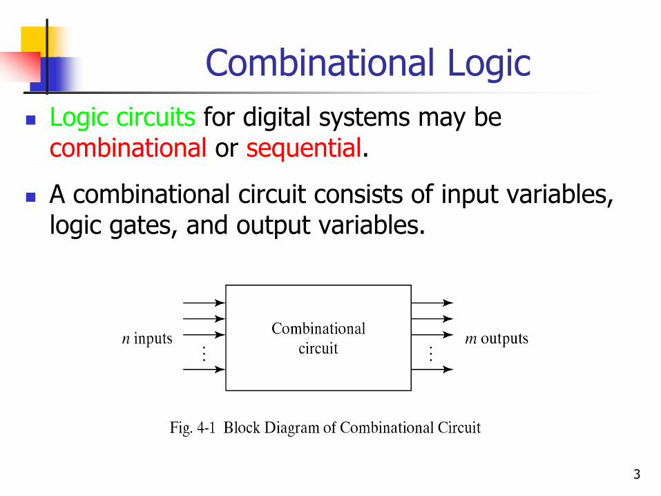
Combinational Logicn Logic circuits for digital systems may be
combinational or sequential.n A combinational circuit consists of input variables,
logic gates, and output variables.
4
4-2. Analysis proceduren To obtain the output Boolean functions from a
logic diagram, proceed as follows:
1. Label all gate outputs that are a function of input variables with arbitrary symbols. Determine the Boolean functions for each gate output.
2. Label the gates that are a function of input variables and previously labeled gates with other arbitrary symbols. Find the Boolean functions for these gates.

5
Analysis procedure3. Repeat the process outlined in step 2 until the outputs of
the circuit are obtained.
4. By repeated substitution of previously defined functions, obtain the output Boolean functions in terms of input variables.
6
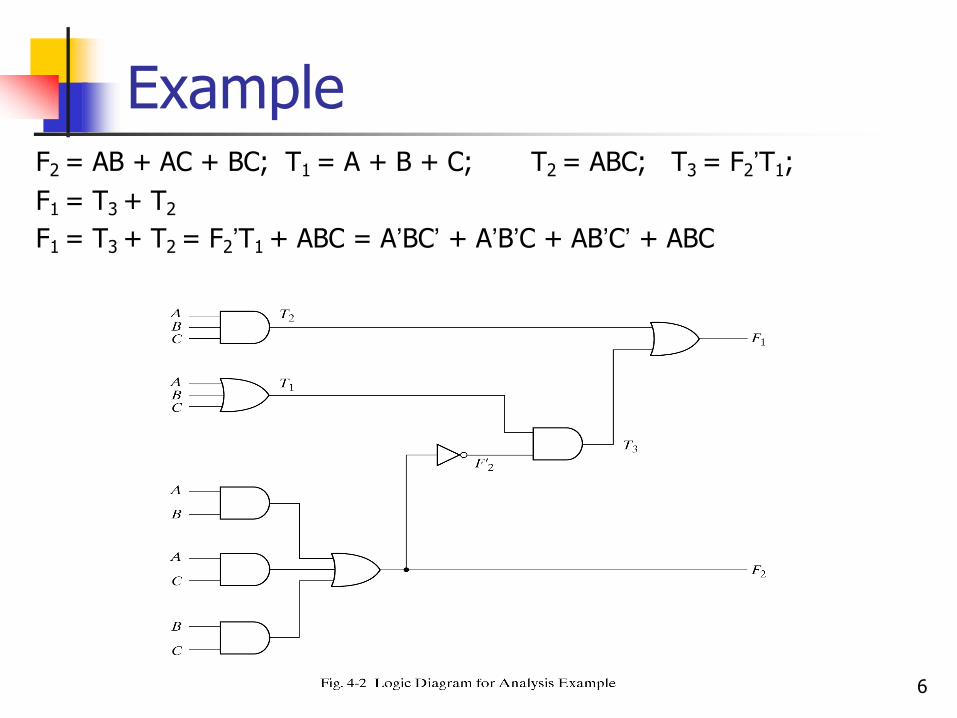
ExampleF2 = AB + AC + BC; T1 = A + B + C; T2 = ABC; T3 = F2’T1; F1 = T3 + T2
F1 = T3 + T2 = F2’T1 + ABC = A’BC’ + A’B’C + AB’C’ + ABC
7
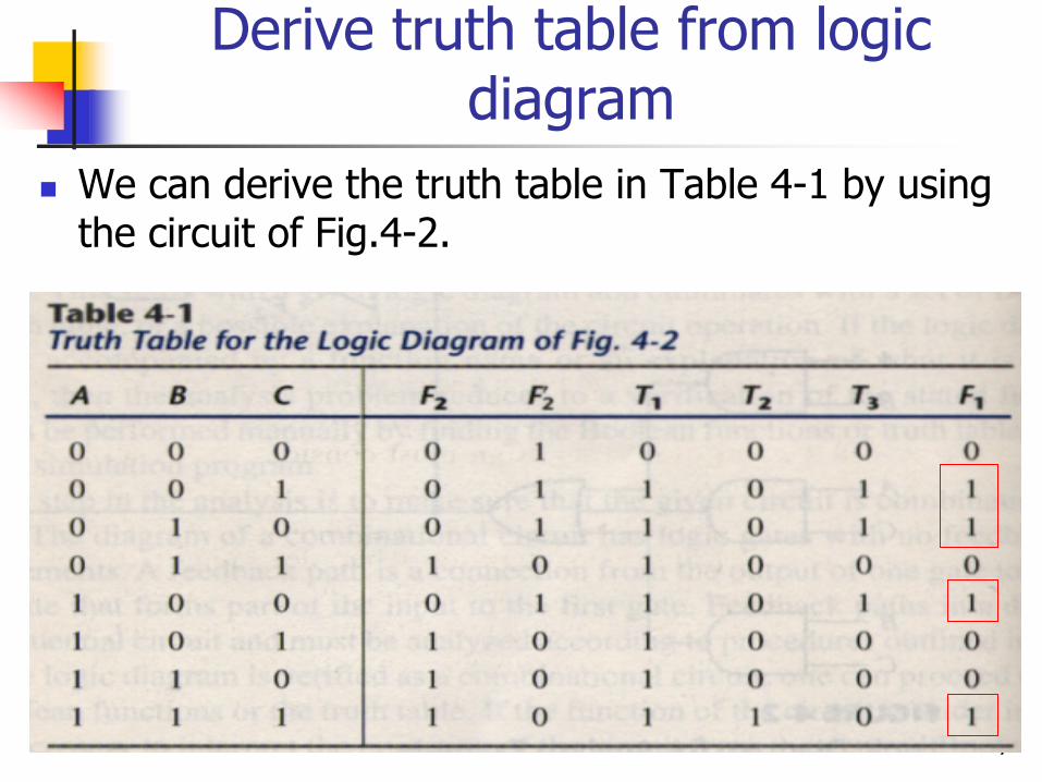
Derive truth table from logic diagram
n We can derive the truth table in Table 4-1 by using the circuit of Fig.4-2.

8
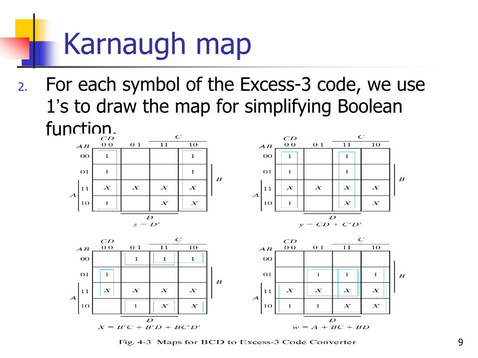
Design procedure1. Table4-2 is a Code-Conversion example, first,
we can list the relation of the BCD and Excess-3 codes in the truth table.
9
Karnaugh map2. For each symbol of the Excess-3 code, we use
1’s to draw the map for simplifying Boolean function.
10
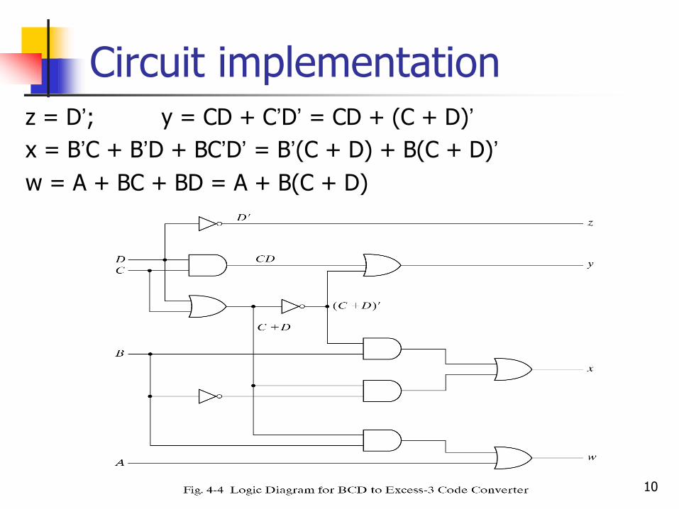
Circuit implementationz = D’; y = CD + C’D’ = CD + (C + D)’x = B’C + B’D + BC’D’ = B’(C + D) + B(C + D)’w = A + BC + BD = A + B(C + D)
11
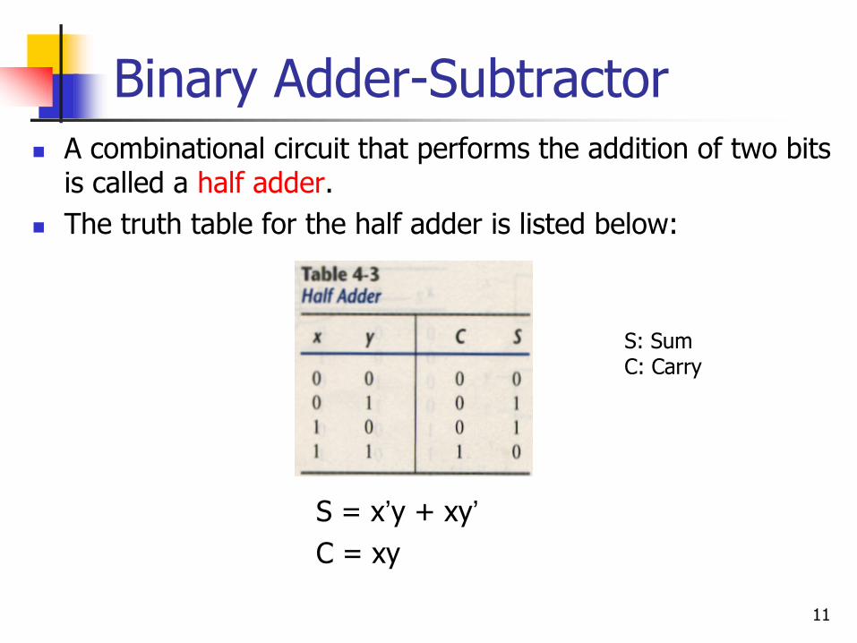
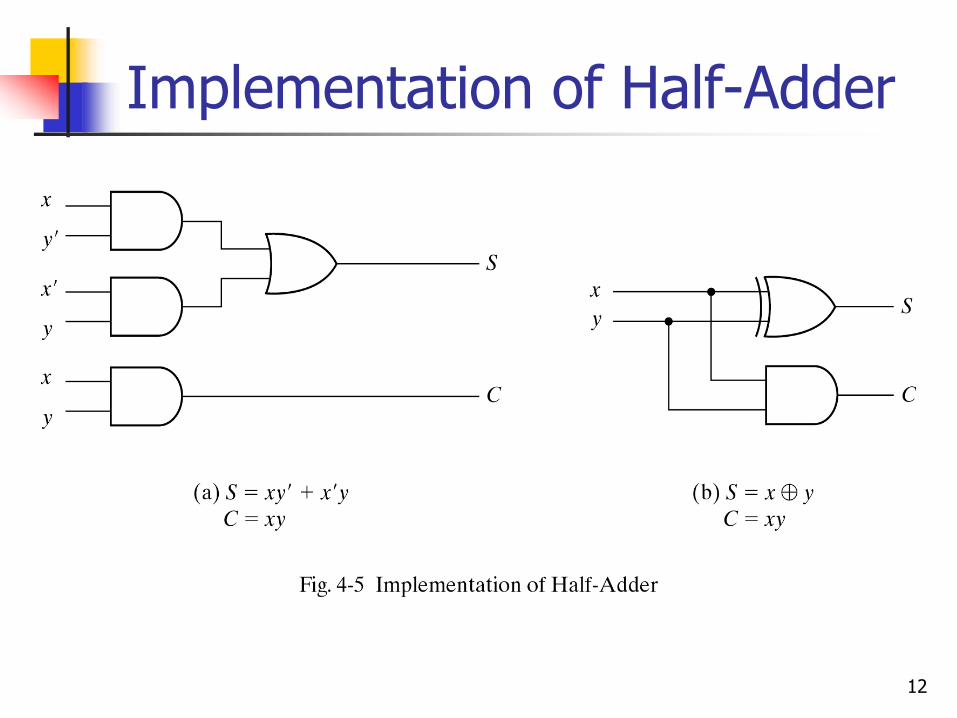
Binary Adder-Subtractorn A combinational circuit that performs the addition of two bits
is called a half adder.n The truth table for the half adder is listed below:
S = x’y + xy’ C = xy
S: SumC: Carry
12
Implementation of Half-Adder
13
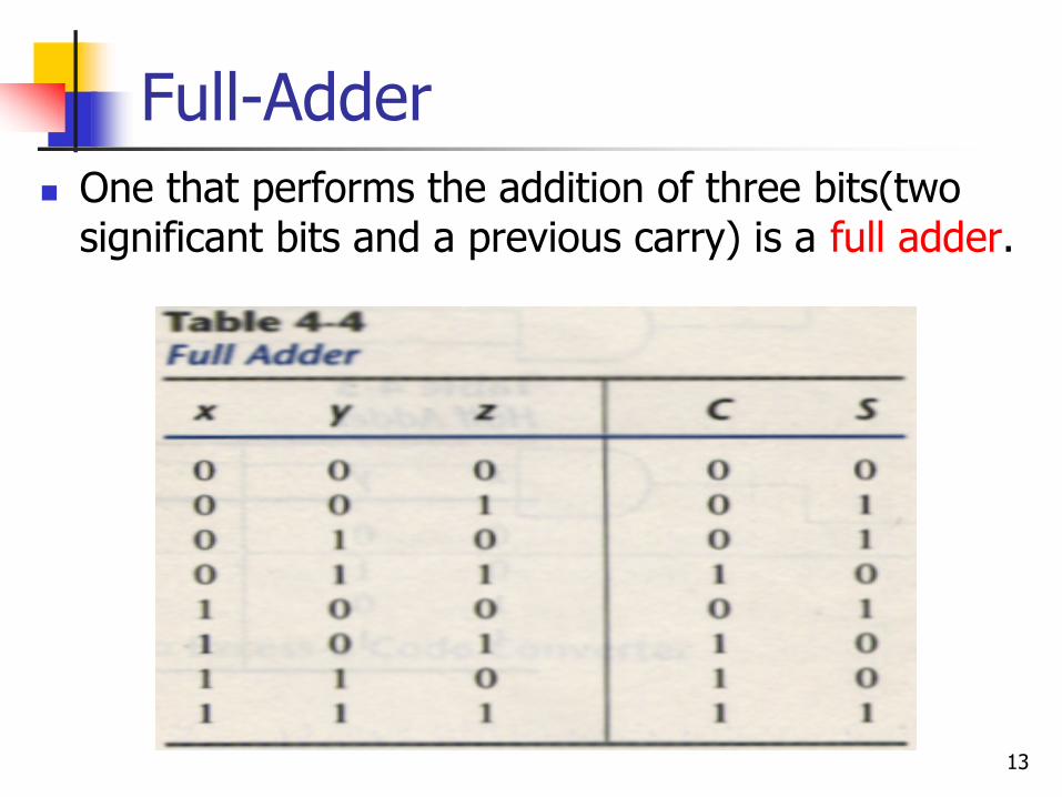
Full-Addern One that performs the addition of three bits(two
significant bits and a previous carry) is a full adder.
14
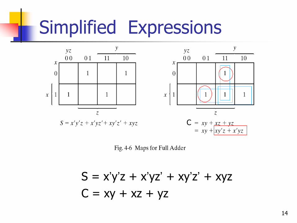
Simplified Expressions
S = x’y’z + x’yz’ + xy’z’ + xyz C = xy + xz + yz
C

15
Full adder implemented in SOP
16
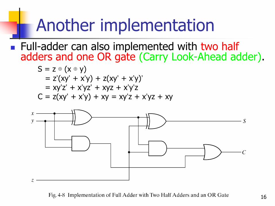
Another implementationn Full-adder can also implemented with two half
adders and one OR gate (Carry Look-Ahead adder).S = z ⊕ (x ⊕ y) = z’(xy’ + x’y) + z(xy’ + x’y)’ = xy’z’ + x’yz’ + xyz + x’y’zC = z(xy’ + x’y) + xy = xy’z + x’yz + xy
17
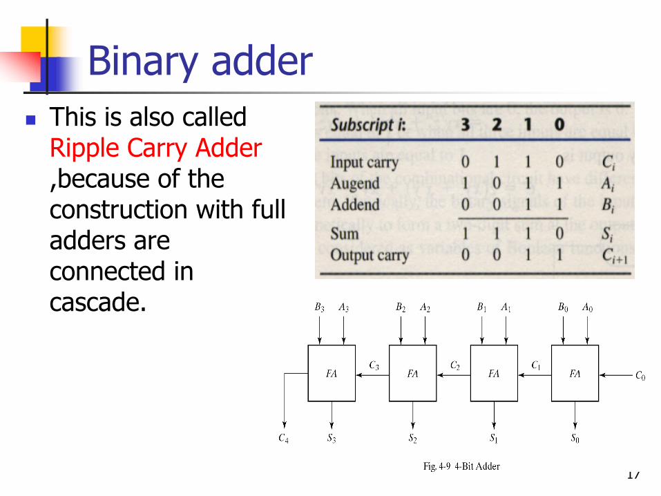
Binary addern This is also called
Ripple Carry Adder ,because of the construction with full adders are connected in cascade.

18
Carry Propagation
n Fig.4-9 causes a unstable factor on carry bit, and produces a longest propagation delay.
n The signal from Ci to the output carry Ci+1, propagates through an AND and OR gates, so, for an n-bit RCA, there are 2n gate levels for the carry to propagate from input to output.
19
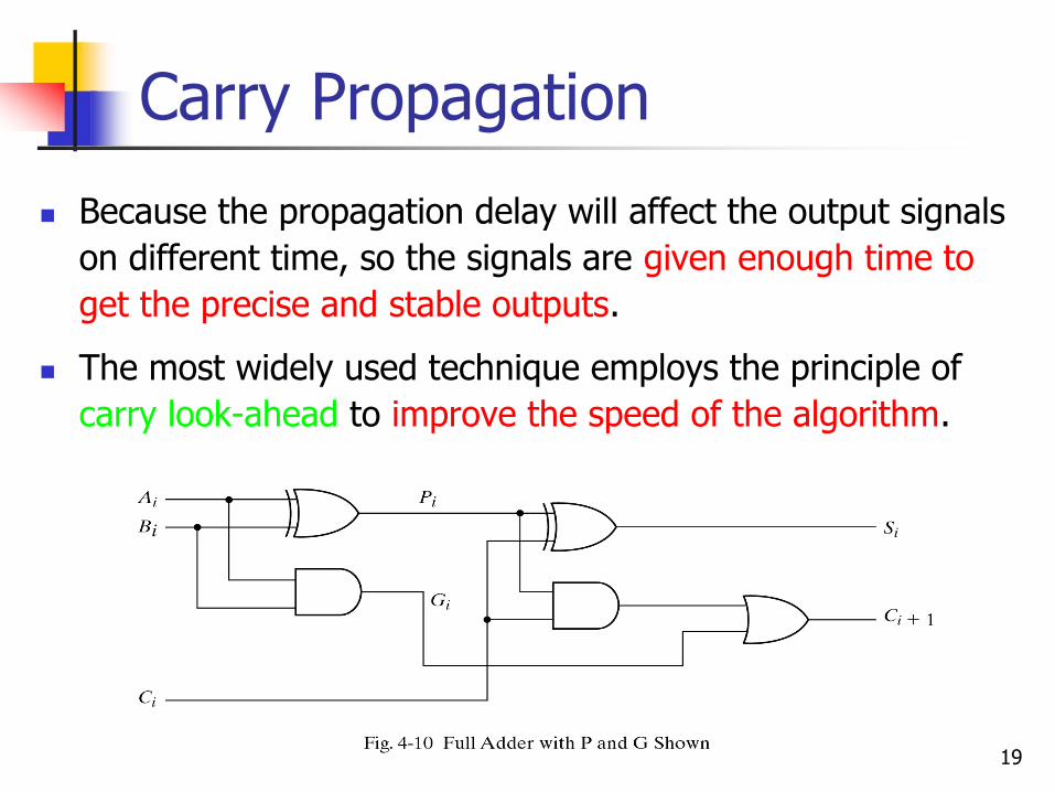
Carry Propagationn Because the propagation delay will affect the output signals
on different time, so the signals are given enough time to get the precise and stable outputs.
n The most widely used technique employs the principle of carry look-ahead to improve the speed of the algorithm.
20
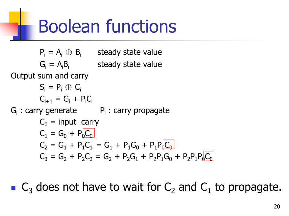
Boolean functionsPi = Ai ⊕ Bi steady state valueGi = AiBi steady state value
Output sum and carrySi = Pi ⊕ Ci
Ci+1 = Gi + PiCi
Gi : carry generate Pi : carry propagateC0 = input carryC1 = G0 + P0C0
C2 = G1 + P1C1 = G1 + P1G0 + P1P0C0
C3 = G2 + P2C2 = G2 + P2G1 + P2P1G0 + P2P1P0C0
n C3 does not have to wait for C2 and C1 to propagate.
21
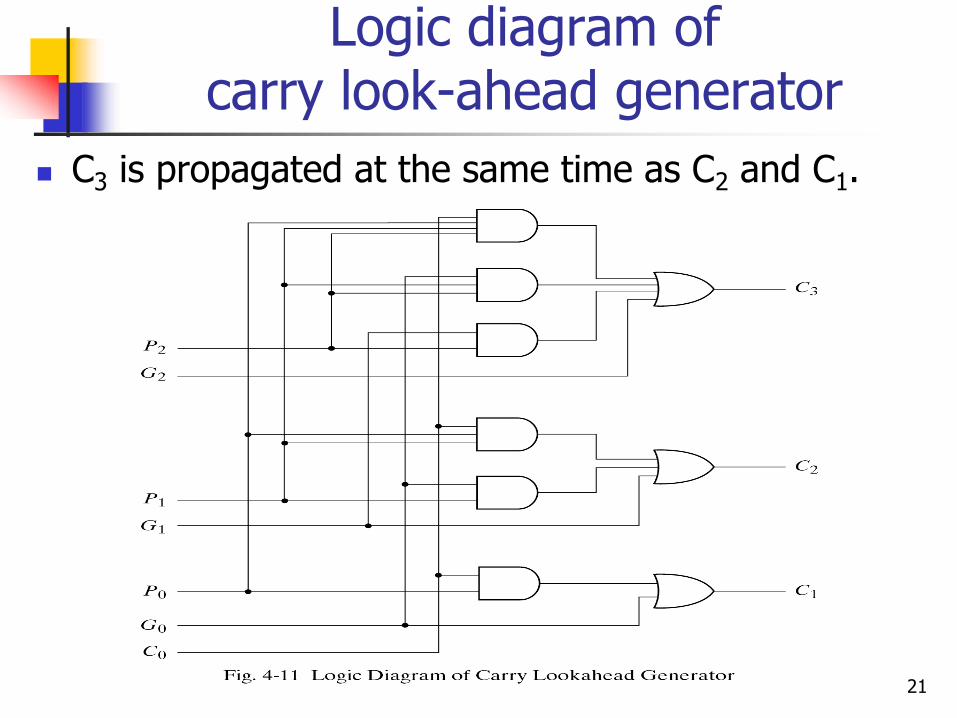
Logic diagram of carry look-ahead generator
n C3 is propagated at the same time as C2 and C1.
22
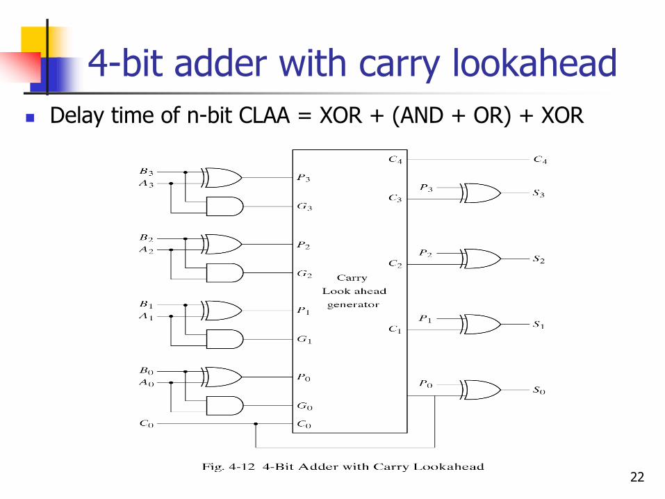
4-bit adder with carry lookaheadn Delay time of n-bit CLAA = XOR + (AND + OR) + XOR
23
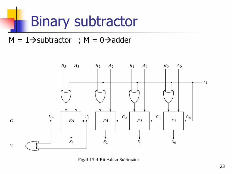
Binary subtractorM = 1subtractor ; M = 0adder
24
Overflown It is worth noting Fig.4-13 that binary numbers in the signed
-complement system are added and subtracted by the same basic addition and subtraction rules as unsigned numbers.
n Overflow is a problem in digital computers because the number of bits that hold the number is finite and a result that contains n+1 bits cannot be accommodated.
25
Overflow on signed and unsignedn When two unsigned numbers are added, an overflow is
detected from the end carry out of the MSB position.
n When two signed numbers are added, the sign bit is treated as part of the number and the end carry does not indicate an overflow.
n An overflow cann’t occur after an addition if one number is positive and the other is negative.
n An overflow may occur if the two numbers added are both positive or both negative.
26
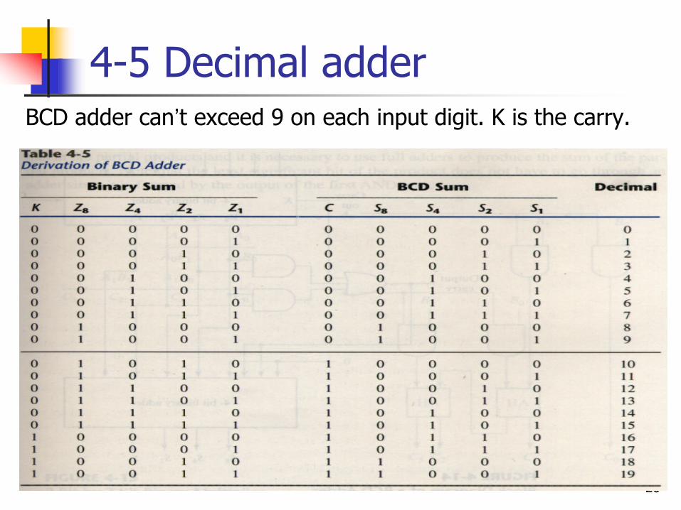
4-5 Decimal adderBCD adder can’t exceed 9 on each input digit. K is the carry.
27
Rules of BCD addern When the binary sum is greater than 1001, we obtain a non-
valid BCD representation.
n The addition of binary 6(0110) to the binary sum converts it to the correct BCD representation and also produces an output carry as required.
n To distinguish them from binary 1000 and 1001, which also have a 1 in position Z8, we specify further that either Z4 or Z2 must have a 1.
C = K + Z8Z4 + Z8Z2

28
Implementation of BCD addern A decimal parallel
adder that adds n decimal digits needs n BCD adder stages.
n The output carry from one stage must be connected to the input carry of the next higher-order stage.
If =1
0110
29
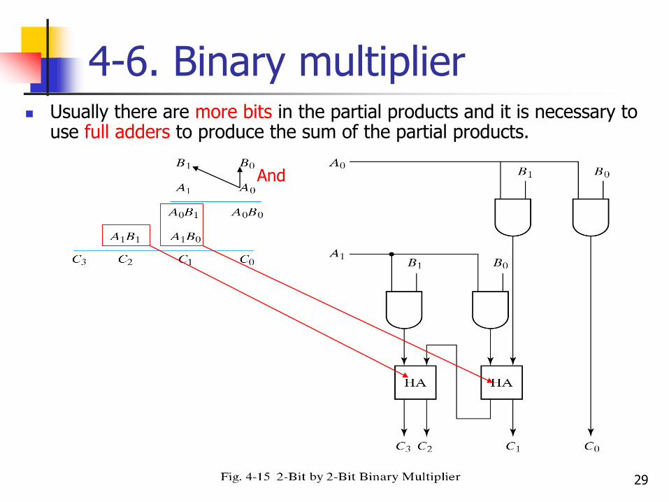
4-6. Binary multipliern Usually there are more bits in the partial products and it is necessary to
use full adders to produce the sum of the partial products.
And

30
4-bit by 3-bit binary multipliern For J multiplier bits and K
multiplicand bits we need (J X K) AND gates and (J − 1) K-bit adders to produce a product of J+K bits.
n K=4 and J=3, we need 12 AND gates and two 4-bit adders.

31
4-7. Magnitude comparatorn The equality relation of each
pair of bits can be expressed logically with an exclusive-NOR function as:
A = A3A2A1A0 ; B = B3B2B1B0
xi=AiBi+Ai’Bi’ for i = 0, 1, 2, 3
(A = B) = x3x2x1x0
32
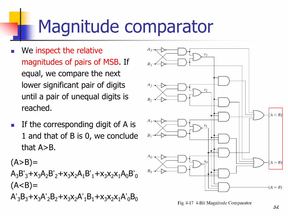
Magnitude comparatorn We inspect the relative
magnitudes of pairs of MSB. If equal, we compare the next lower significant pair of digits until a pair of unequal digits is reached.
n If the corresponding digit of A is 1 and that of B is 0, we conclude that A>B.
(A>B)=A3B’3+x3A2B’2+x3x2A1B’1+x3x2x1A0B’0(A<B)=A’3B3+x3A’2B2+x3x2A’1B1+x3x2x1A’0B0

33
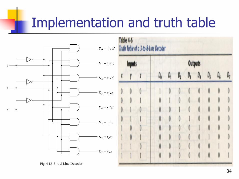
4-8. Decodersn The decoder is called n-to-m-line decoder, where
m≤2n .
n the decoder is also used in conjunction with other code converters such as a BCD-to-seven_segment decoder.
n 3-to-8 line decoder: For each possible input combination, there are seven outputs that are equal to 0 and only one that is equal to 1.
34
Implementation and truth table
35
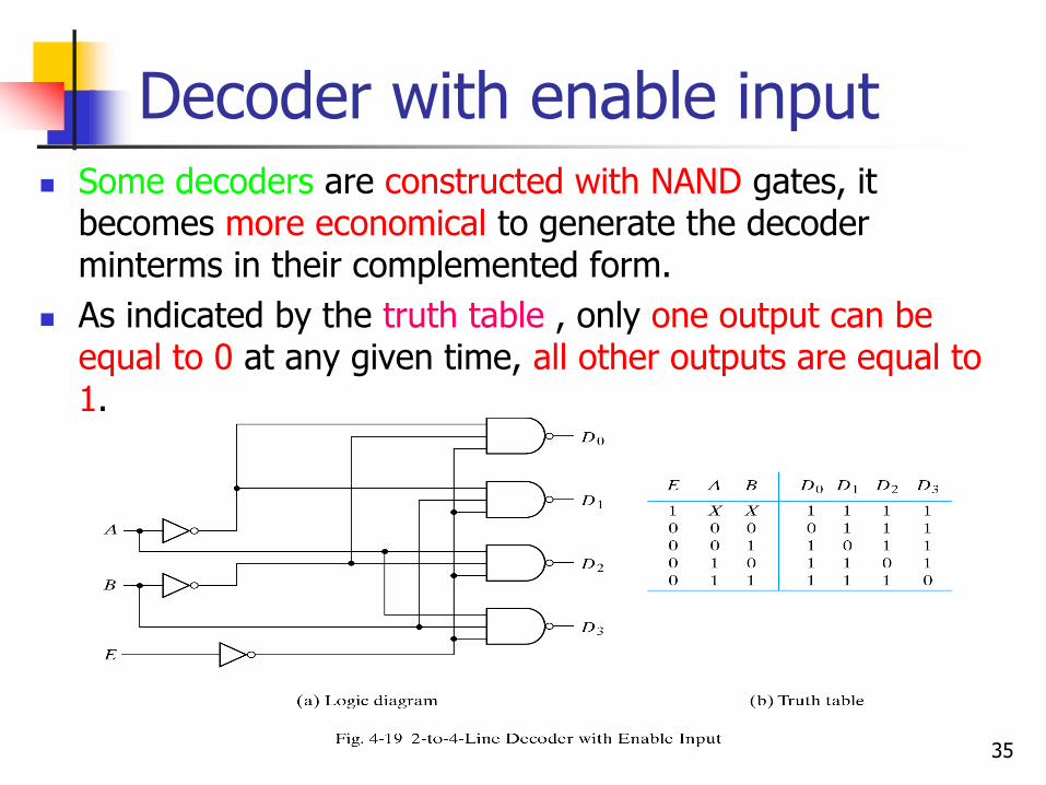
Decoder with enable inputn Some decoders are constructed with NAND gates, it
becomes more economical to generate the decoder minterms in their complemented form.
n As indicated by the truth table , only one output can be equal to 0 at any given time, all other outputs are equal to 1.
36
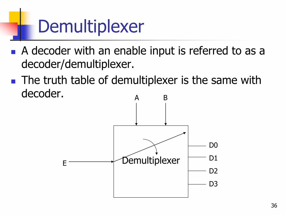
Demultiplexern A decoder with an enable input is referred to as a
decoder/demultiplexer.n The truth table of demultiplexer is the same with
decoder.
DemultiplexerD0D1D2D3
E
A B
37
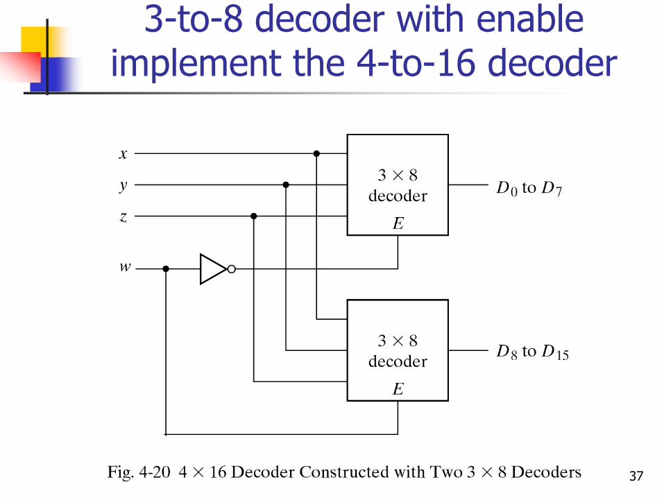
3-to-8 decoder with enable implement the 4-to-16 decoder
38
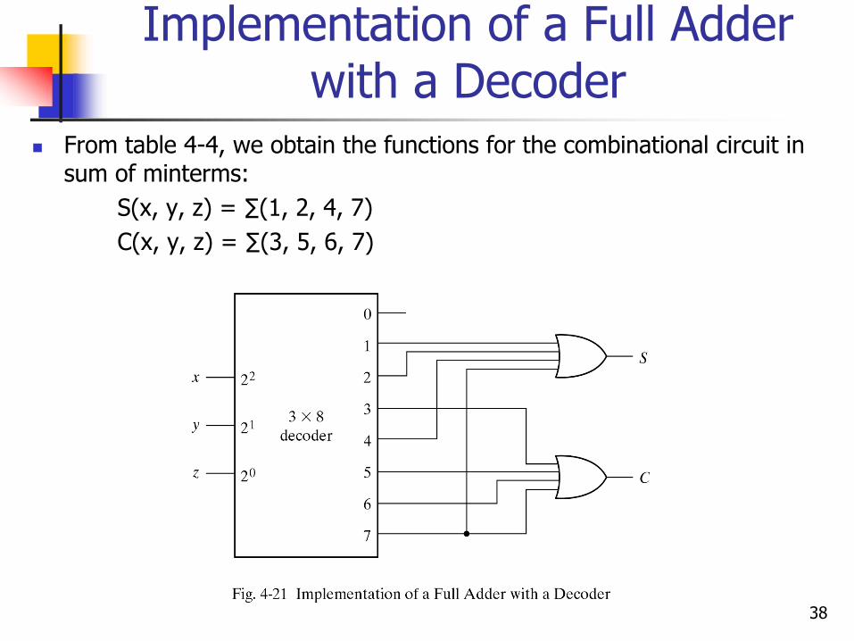
Implementation of a Full Adder with a Decoder
n From table 4-4, we obtain the functions for the combinational circuit in sum of minterms:
S(x, y, z) = ∑(1, 2, 4, 7)C(x, y, z) = ∑(3, 5, 6, 7)

39
4-9. Encodersn An encoder is the inverse operation of a decoder.n We can derive the Boolean functions by table 4-7
z = D1 + D3 + D5 + D7
y = D2 + D3 + D6 + D7
x = D4 + D5 + D6 + D7
40
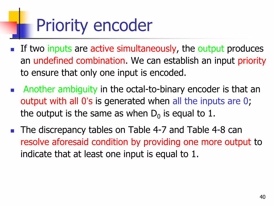
Priority encodern If two inputs are active simultaneously, the output produces
an undefined combination. We can establish an input priorityto ensure that only one input is encoded.
n Another ambiguity in the octal-to-binary encoder is that an output with all 0’s is generated when all the inputs are 0; the output is the same as when D0 is equal to 1.
n The discrepancy tables on Table 4-7 and Table 4-8 can resolve aforesaid condition by providing one more output to indicate that at least one input is equal to 1.
41
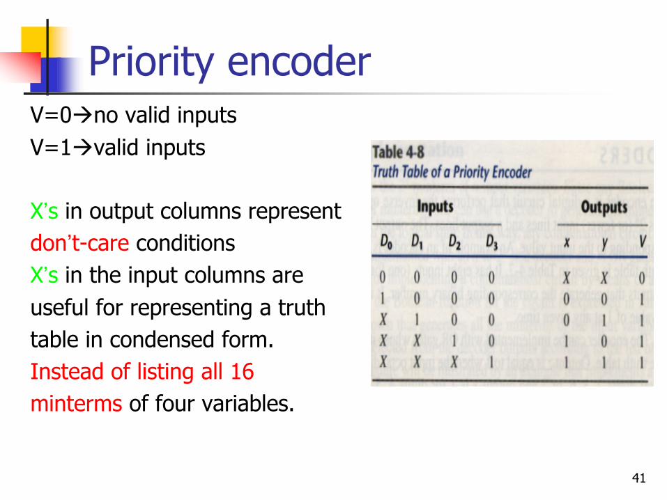
Priority encoderV=0no valid inputsV=1valid inputs
X’s in output columns represent don’t-care conditionsX’s in the input columns are useful for representing a truth table in condensed form. Instead of listing all 16 minterms of four variables.
42
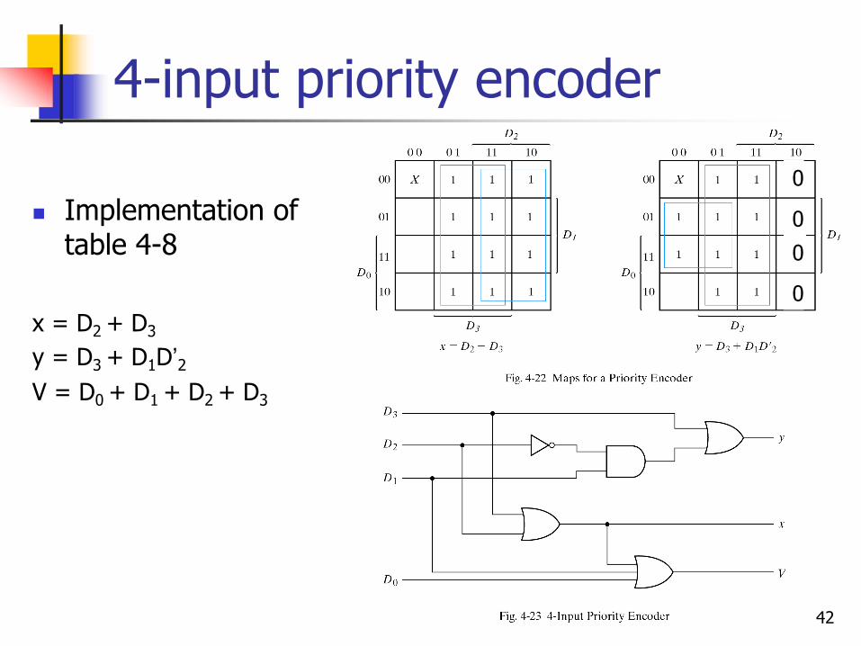
4-input priority encoder
n Implementation of table 4-8
x = D2 + D3y = D3 + D1D’2V = D0 + D1 + D2 + D3
0
00
0
43
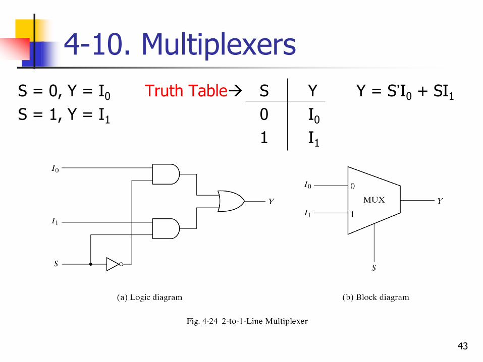
4-10. MultiplexersS = 0, Y = I0 Truth Table S Y Y = S’I0 + SI1
S = 1, Y = I1 0 I0
1 I1
44
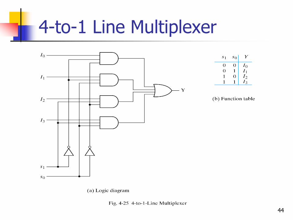
4-to-1 Line Multiplexer
45
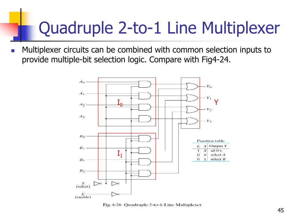
Quadruple 2-to-1 Line Multiplexern Multiplexer circuits can be combined with common selection inputs to
provide multiple-bit selection logic. Compare with Fig4-24.
I0
I1
Y
46
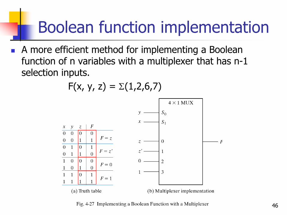
Boolean function implementationn A more efficient method for implementing a Boolean
function of n variables with a multiplexer that has n-1 selection inputs.
F(x, y, z) = (1,2,6,7)

47
4-input function with a multiplexer
F(A, B, C, D) = (1, 3, 4, 11, 12, 13, 14, 15)