Embed Size (px)
Citation preview
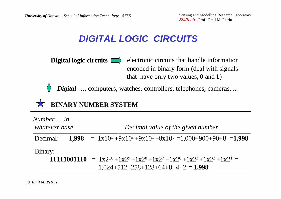
BINARY NUMBER SYSTEM
electronic circuits that handle informationencoded in binary form (deal with signalsthat have only two values, 0 and 1)
Digital …. computers, watches, controllers, telephones, cameras, ...
Digital logic circuits
Number ….inwhatever base Decimal value of the given number
___________________________________________________________________________________________________________________________________________________________________
Decimal: 1,998 = 1x10³ +9x10² +9x101 +8x100 =1,000+900+90+8 =1,998
Binary:11111001110 = 1x210 +1x29 +1x28 +1x27 +1x26 +1x23 +1x22 +1x21 =
1,024+512+258+128+64+8+4+2 = 1,998
© Emil M. Petriu
Sensing and Modelling Research LaboratorySMRLab - Prof.. Emil M. Petriu
University of Ottawa - School of Information Technology - SITE
DIGITAL LOGIC CIRCUITS
____________________________________________________________________________________________________________________________________________________________________
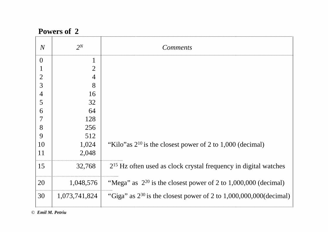
N 2N Comments_____________________________________________________________________________________________________________________________________________________________________
0 11 22 43 84 165 326 647 1288 2569 51210 1,024 “Kilo”as 210 is the closest power of 2 to 1,000 (decimal)11 2,048
……………………………………………………….....
15 32,768 215 Hz often used as clock crystal frequency in digital watches…………………………………………………….....
20 1,048,576 “Mega” as 220 is the closest power of 2 to 1,000,000 (decimal)…………………………………………………...
30 1,073,741,824 “Giga” as 230 is the closest power of 2 to 1,000,000,000(decimal)____________________________________________________________________________________________________________________________________________________________________
Powers of 2
© Emil M. Petriu
_____________________________________________________________
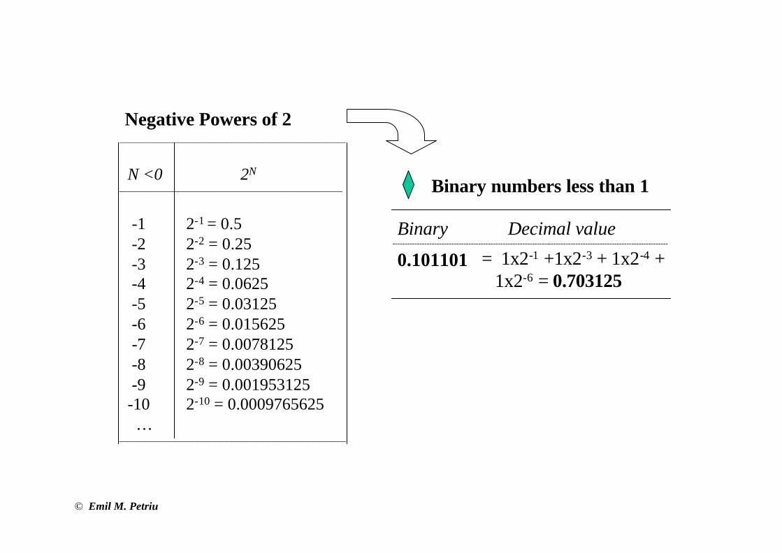
N <0 2N____________________________________________________________
-1 2-1 = 0.5-2 2-2 = 0.25-3 2-3 = 0.125-4 2-4 = 0.0625-5 2-5 = 0.03125-6 2-6 = 0.015625-7 2-7 = 0.0078125-8 2-8 = 0.00390625-9 2-9 = 0.001953125-10 2-10 = 0.0009765625…
_____________________________________________________________
Negative Powers of 2
Binary numbers less than 1
= 1x2-1 +1x2-3 + 1x2-4 +1x2-6 = 0.703125
Binary Decimal value-----------------------------------------------------------------------------------------------------------------
0.101101
© Emil M. Petriu
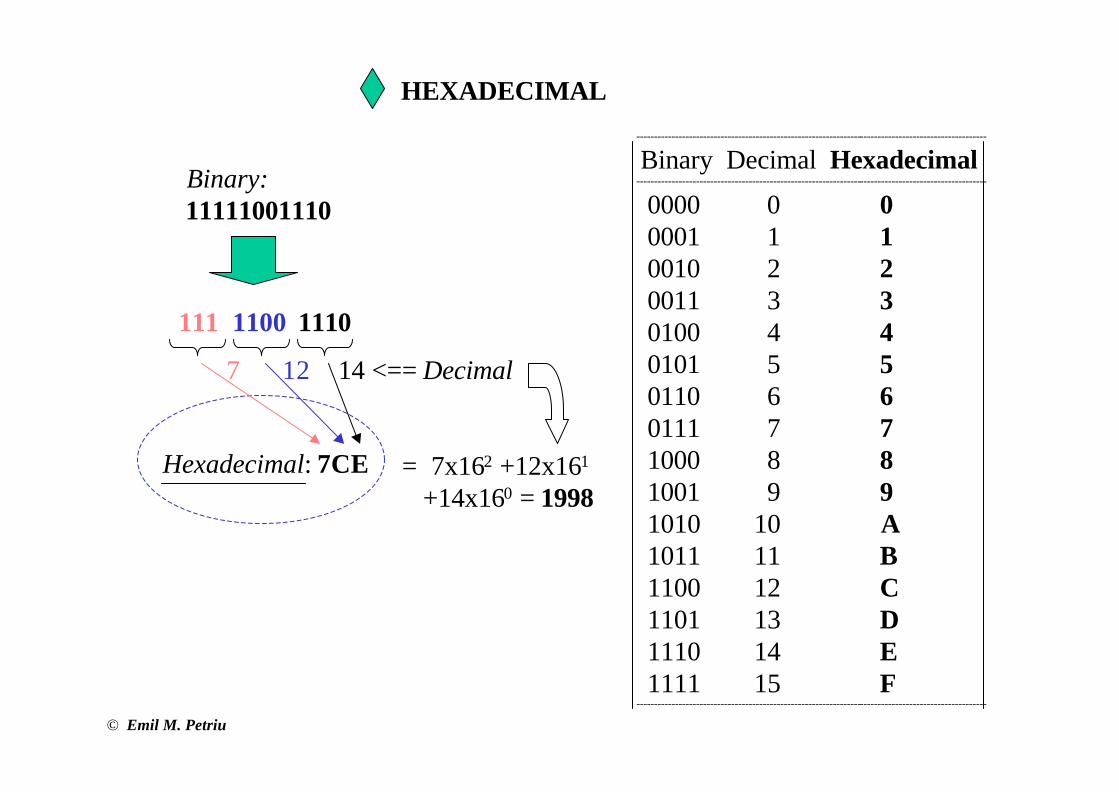
Hexadecimal: 7CE
7 12 14 <== Decimal
111 1100 1110
11111001110Binary:
= 7x162 +12x161
+14x160 = 1998
----------------------------------------------------------------------------------------------------
Binary Decimal Hexadecimal----------------------------------------------------------------------------------------------------
0000 0 00001 1 10010 2 20011 3 30100 4 40101 5 50110 6 60111 7 71000 8 81001 9 91010 10 A1011 11 B1100 12 C1101 13 D1110 14 E1111 15 F
----------------------------------------------------------------------------------------------------
HEXADECIMAL
© Emil M. Petriu
LOGIC OPERATIONS AND TRUTH TABLES
Digital logic circuits handle data encoded in binary form, i.e. signalsthat have only two values, 0 and 1.
Binary logic dealing with “true” and “false” comes in handy to describethe behaviour of these circuits: 0 is usually associated with “false” and1 with “true.”
Quite complex digital logic circuits (e.g. entire computers) can be built using a few types of basic circuits called gates, each performing a single elementary logic operation : NOT, AND, OR, NAND, NOR, etc..
Boole’s binary algebra is used as a formal / mathematical tool to describe and design complex binary logic circuits.
© Emil M. Petriu
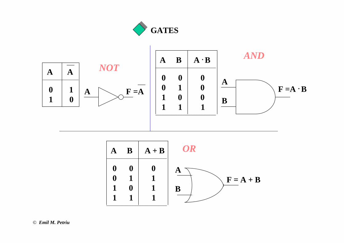
A B A + B_____________________________________
0 0 00 1 11 0 11 1 1
_____________________________________
A
BF = A + B
OR
A F =A
A A______________________
0 11 0
NOTA
BF =A . B
A B A . B_____________________________________
0 0 00 1 01 0 01 1 1
_____________________________________
AND
GATES
© Emil M. Petriu
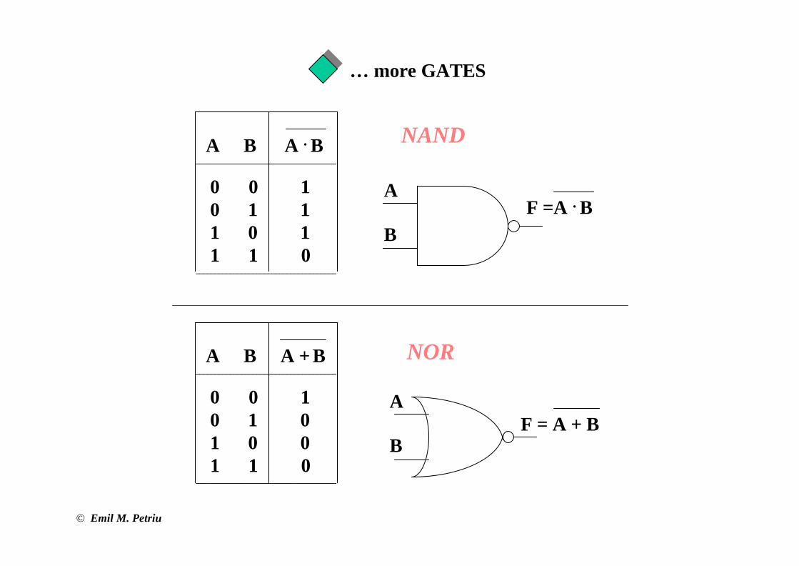
NANDA B A . B_____________________________________
0 0 10 1 11 0 11 1 0
_____________________________________
NORA B A + B_____________________________________
0 0 10 1 01 0 01 1 0
_____________________________________
A
BF =A . B
A
BF = A + B
… more GATES
© Emil M. Petriu
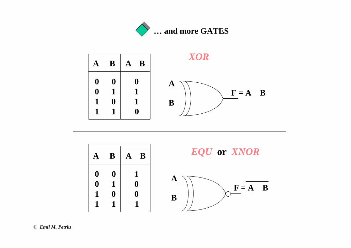
XOR
A
BF = A B⊕
A B A B_____________________________________
0 0 00 1 11 0 11 1 0
_____________________________________
⊕
EQU or XNOR
A
BF = A B⊕
A B A B_____________________________________
0 0 10 1 01 0 01 1 1
_____________________________________
⊕
… and more GATES
© Emil M. Petriu
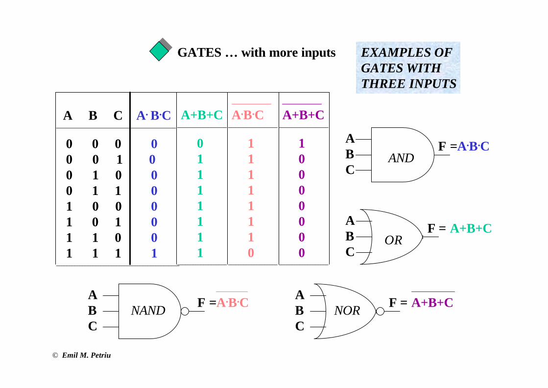
GATES … with more inputs
A B C A. B.C______________________________________________
0 0 0 0 0 0 1 00 1 0 00 1 1 01 0 0 01 0 1 01 1 0 01 1 1 1
_______________________________________________
F =A.B.CABC
F =A.B.CABC
F = A+B+CABC
F = A+B+CABC
A+B+C___________________
01111111
___________________
A.B.C___________________
11111110
___________________
A+B+C___________________
10000000
___________________
AND
OR
NAND NOR
EXAMPLES OF GATES WITH THREE INPUTS
© Emil M. Petriu
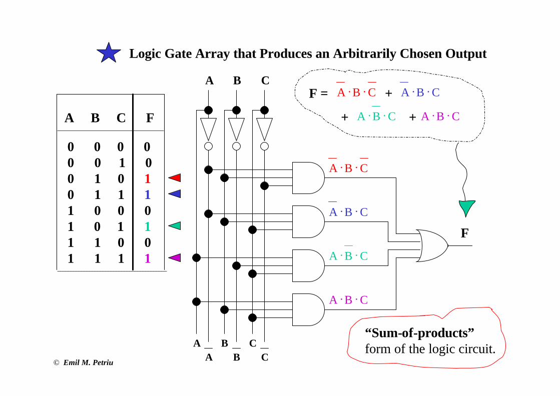
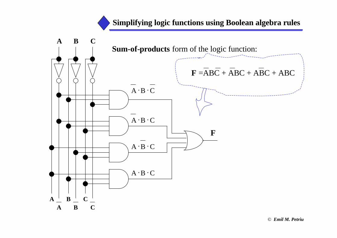
Logic Gate Array that Produces an Arbitrarily Chosen Output
A B C F________________________________________
0 0 0 0 0 0 1 00 1 0 10 1 1 11 0 0 01 0 1 11 1 0 01 1 1 1
_________________________________________
A B C
A B CA B C
A . B . C
A . B . C
A . B . C
F
F =
+ A . B . C
A . B . C + A . B . C
+ A . B . C
A . B . C
“Sum-of-products”form of the logic circuit.
© Emil M. Petriu
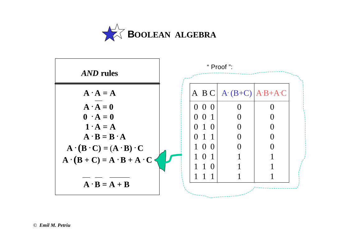
BOOLEAN ALGEBRA
AND rules
A . A = A
A . A = 00 . A = 01 . A = AA . B = B . A
A . (B . C) = (A . B) . CA . (B + C) = A . B + A . C
A . B = A + B
A B C A. (B+C) A.B+A.C____________________________________________________________
0 0 0 0 00 0 1 0 00 1 0 0 00 1 1 0 01 0 0 0 01 0 1 1 11 1 0 1 11 1 1 1 1
“ Proof ”:
© Emil M. Petriu
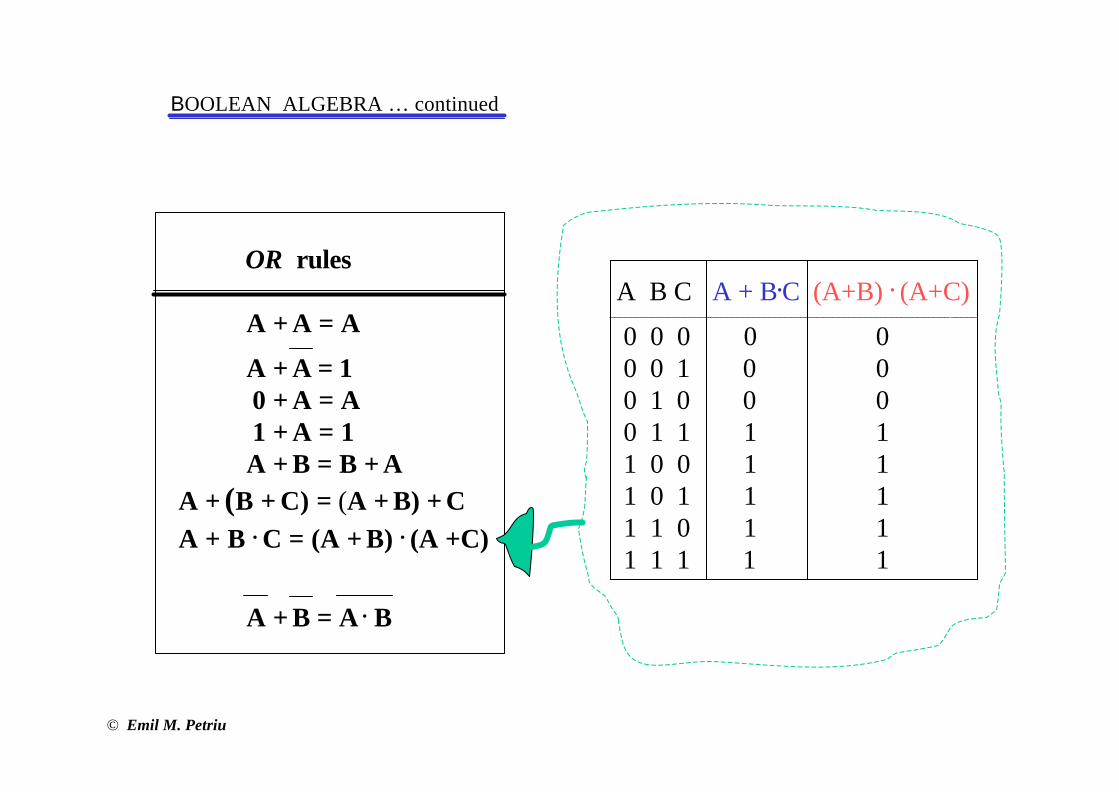
OR rules
A + A = A
A + A = 10 + A = A1 + A = 1A + B = B + A
A + (B + C) = (A + B) + CA + B . C = (A + B) . (A +C)
A + B = A . B
A B C A + B.C (A+B) . (A+C)_____________________________________________________________________
0 0 0 0 00 0 1 0 00 1 0 0 00 1 1 1 11 0 0 1 11 0 1 1 11 1 0 1 11 1 1 1 1
BOOLEAN ALGEBRA … continued
© Emil M. Petriu
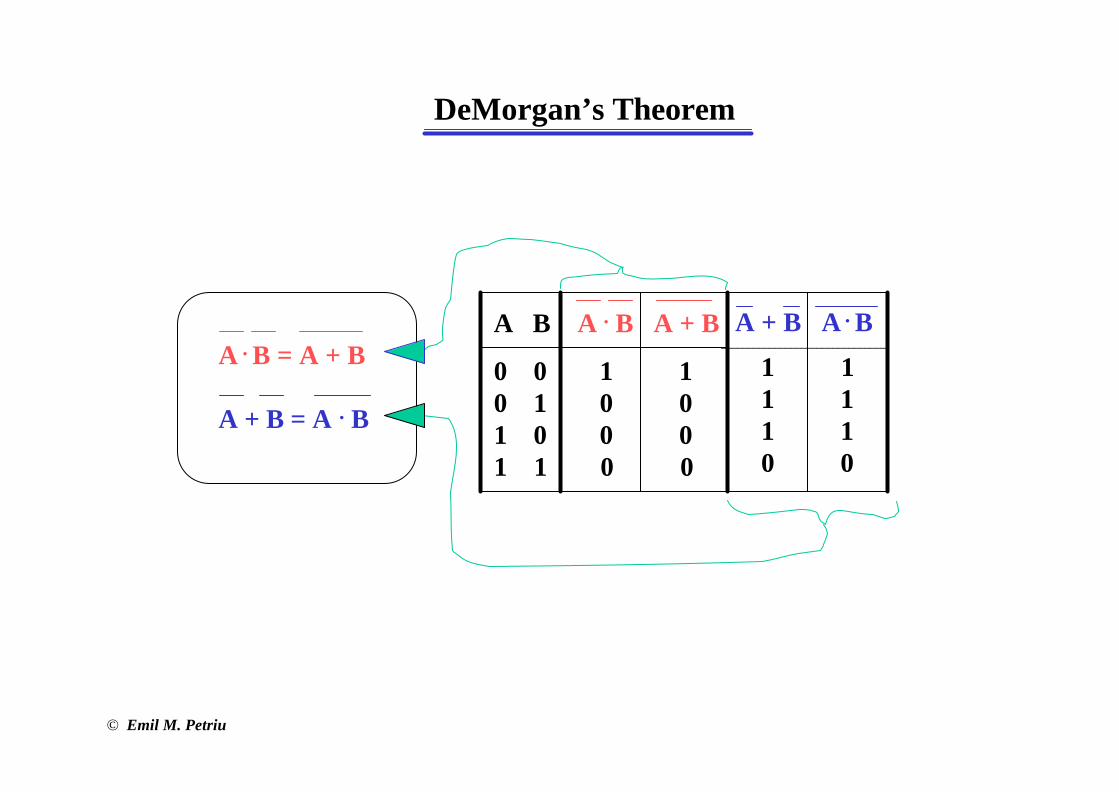
A . B = A + B
A + B = A . B
DeMorgan’s Theorem
A B A . B A + B
0 0 1 10 1 0 01 0 0 01 1 0 0
A + B A . B_______________________________
1 11 11 10 0
© Emil M. Petriu
A B C
A B CA B C
A . B . C
A . B . C
A . B . C
F
A . B . C
F =ABC + ABC + ABC + ABC
Sum-of-products form of the logic function:
Simplifying logic functions using Boolean algebra rules
© Emil M. Petriu
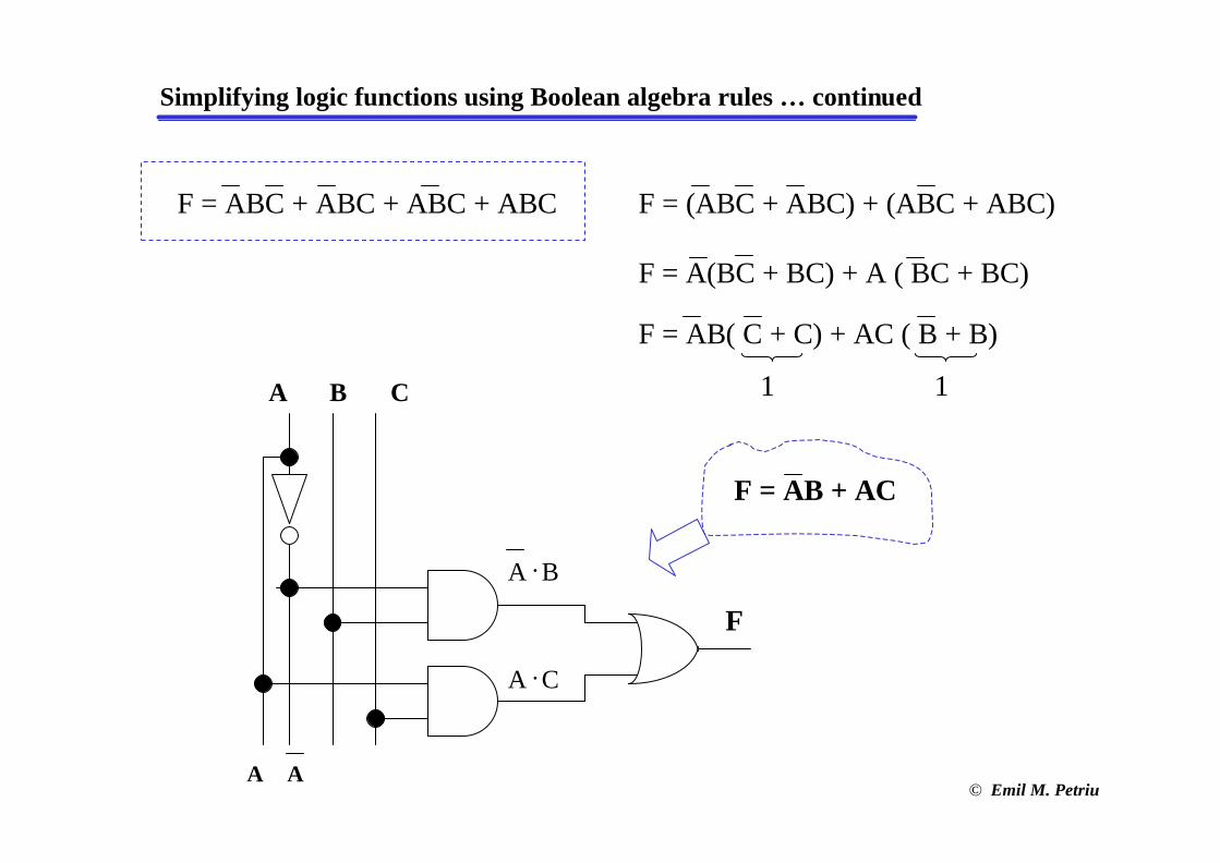
F = ABC + ABC + ABC + ABC F = (ABC + ABC) + (ABC + ABC)
F = A(BC + BC) + A ( BC + BC)
F = AB( C + C) + AC ( B + B)
1 1
Simplifying logic functions using Boolean algebra rules … continued
A B C
A A
A . C
F
A . B
F = AB + AC
© Emil M. Petriu
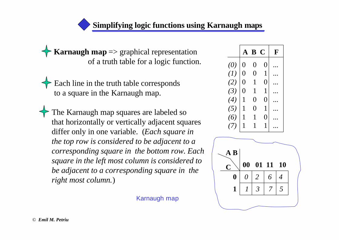
Simplifying logic functions using Karnaugh maps
A B C F
(0) 0 0 0 ...(1) 0 0 1 ...(2) 0 1 0 ...(3) 0 1 1 ...(4) 1 0 0 ...(5) 1 0 1 ...(6) 1 1 0 ...(7) 1 1 1 ...
Each line in the truth table corresponds to a square in the Karnaugh map.
Karnaugh map => graphical representation of a truth table for a logic function.
The Karnaugh map squares are labeled so that horizontally or vertically adjacent squaresdiffer only in one variable. (Each square in the top row is considered to be adjacent to a corresponding square in the bottom row. Each square in the left most column is considered to be adjacent to a corresponding square in theright most column.)
C
A B
00 01 11 10
0 0 2 6 4
1 3 7 51Karnaugh map
© Emil M. Petriu
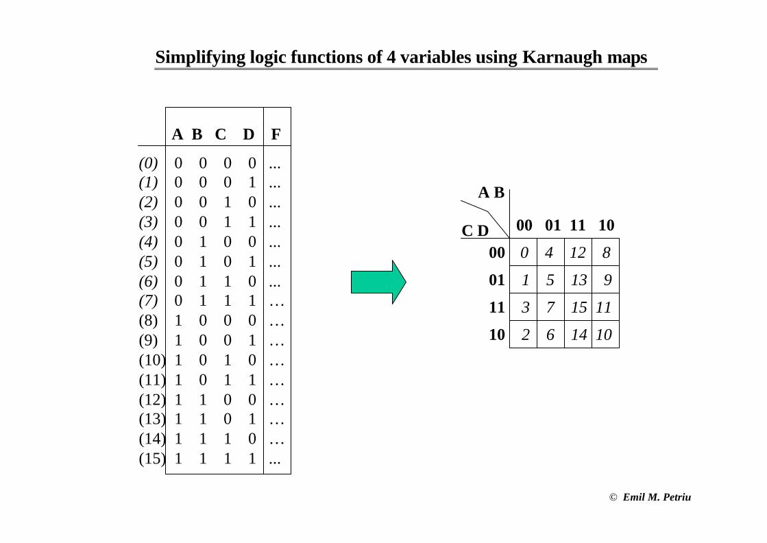
C D
A B
00 01 11 10
00 0 4 12 8
1 5 13 9
3 7 15 11
2 6 14 10
01
11
10
A B C D F
(0) 0 0 0 0 ...(1) 0 0 0 1 ...(2) 0 0 1 0 ...(3) 0 0 1 1 ...(4) 0 1 0 0 ...(5) 0 1 0 1 ...(6) 0 1 1 0 ...(7) 0 1 1 1 …(8) 1 0 0 0 …(9) 1 0 0 1 …(10) 1 0 1 0 …(11) 1 0 1 1 …(12) 1 1 0 0 …(13) 1 1 0 1 …(14) 1 1 1 0 …(15) 1 1 1 1 ...
Simplifying logic functions of 4 variables using Karnaugh maps
© Emil M. Petriu
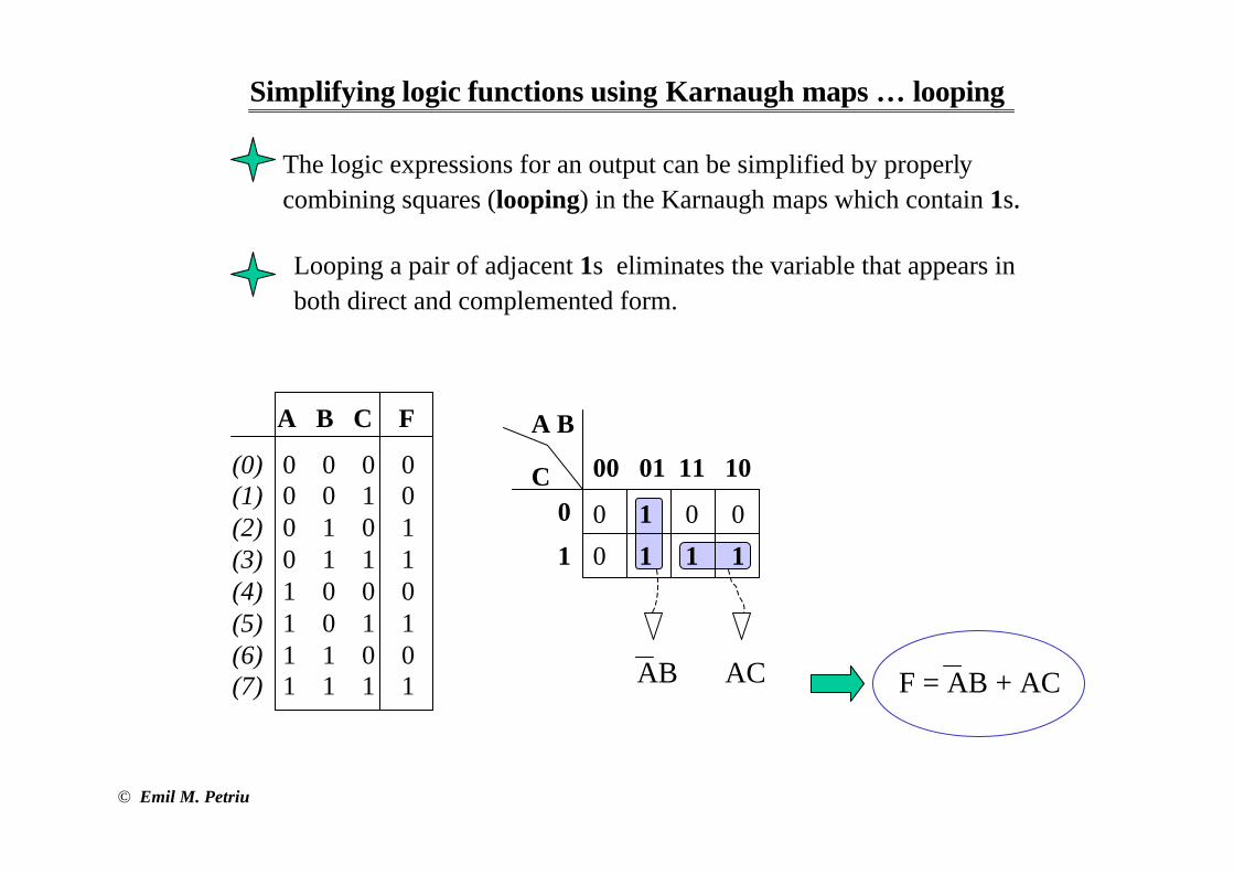
A B C F
(0) 0 0 0 0(1) 0 0 1 0(2) 0 1 0 1(3) 0 1 1 1(4) 1 0 0 0(5) 1 0 1 1(6) 1 1 0 0(7) 1 1 1 1
Simplifying logic functions using Karnaugh maps … looping
The logic expressions for an output can be simplified by properlycombining squares (looping) in the Karnaugh maps which contain 1s.
Looping a pair of adjacent 1s eliminates the variable that appears in both direct and complemented form.
ACAB
C
A B
00 01 11 10
0
1
0 1 0 0
0 1 1 1
F = AB + AC
© Emil M. Petriu
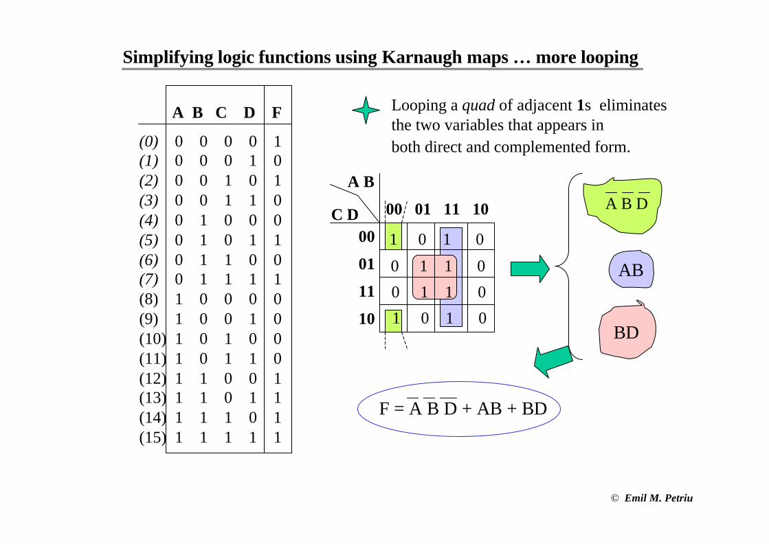
Looping a quad of adjacent 1s eliminates the two variables that appears in both direct and complemented form.
A B C D F
(0) 0 0 0 0 1(1) 0 0 0 1 0(2) 0 0 1 0 1(3) 0 0 1 1 0(4) 0 1 0 0 0(5) 0 1 0 1 1(6) 0 1 1 0 0(7) 0 1 1 1 1(8) 1 0 0 0 0(9) 1 0 0 1 0(10) 1 0 1 0 0(11) 1 0 1 1 0(12) 1 1 0 0 1(13) 1 1 0 1 1(14) 1 1 1 0 1(15) 1 1 1 1 1
Simplifying logic functions using Karnaugh maps … more looping
C D
A B
00 01 11 10
00
01
11
10
1 0 1 0
0 1 1 0
0 1 1 0
1 0 1 0BD
A B D
AB
F = A B D + AB + BD
© Emil M. Petriu
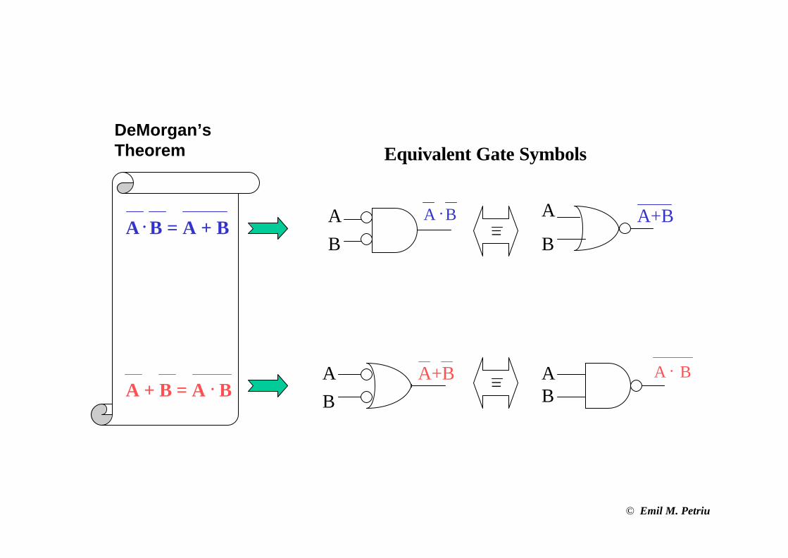
A
BA+BA . B A
B =
A+BAB
A . BAB=
DeMorgan’s Theorem
A . B = A + B
A + B = A . B
Equivalent Gate Symbols
© Emil M. Petriu
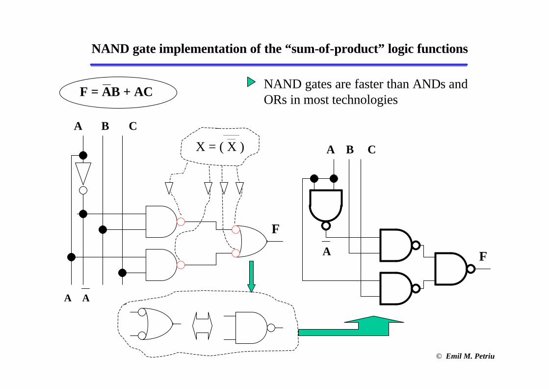
NAND gate implementation of the “sum-of-product” logic functions
NAND gates are faster than ANDs and ORs in most technologies
A B C
A A
F
A B C
FA
F = AB + AC
X = ( X )
© Emil M. Petriu
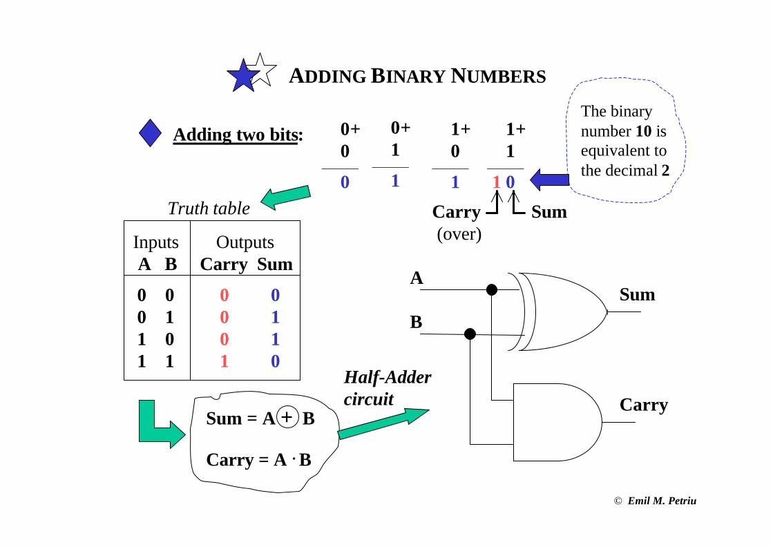
ADDING BINARY NUMBERS
0+1
__________
1
1+0
__________
1
1+1
__________
1 0
The binary number 10 is equivalent to the decimal 2
Carry(over)
Sum
0+0
__________
0
Inputs OutputsA B Carry Sum
0 0 0 00 1 0 11 0 0 11 1 1 0
Truth table
A
BSum
CarrySum = A + B
Carry = A . B
Half-Addercircuit
Adding two bits:
© Emil M. Petriu
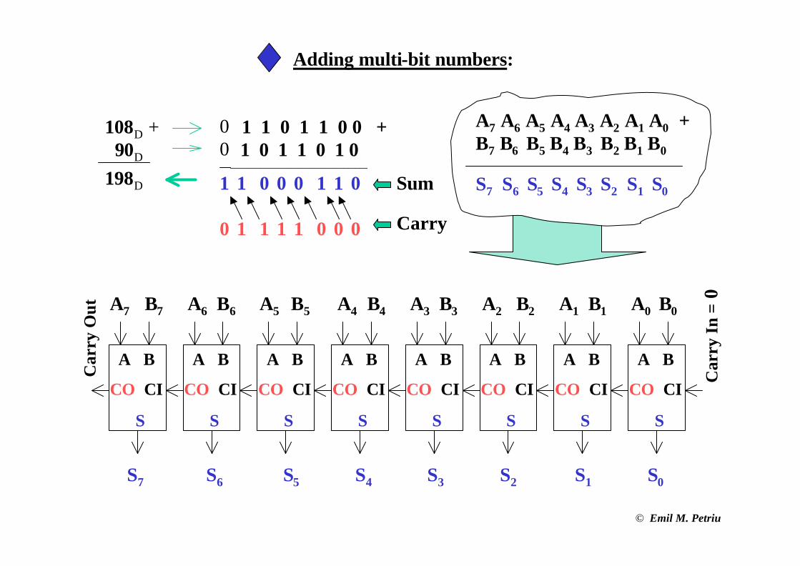
Adding multi-bit numbers:
1 0 1 1 0 1 0____________________________________
1
0
0
0
1
0
0
1
0
1
0
1
1
1
1
0
00
108D +90D
198D
1 1 0 1 1 0 0 +
Sum
Carry
A B
CO CI
S
A B
CO CI
S
A B
CO CI
S
A B
CO CI
S
A B
CO CI
S
A B
CO CI
S
A B
CO CI
S
A B
CO CI
S
S7 S6 S5 S4 S3 S2 S1 S0
A7 B7 A6 B6 A5 B5 A4 B4 A3 B3 A2 B2 A1 B1 A0 B0
Car
ry O
ut
Car
ry I
n =
0
A7 A6 A5 A4 A3 A2 A1 A0 +B7 B6 B5 B4 B3 B2 B1 B0
S7 S6 S5 S4 S3 S2 S1 S0
© Emil M. Petriu
Car
ry O
ut
Car
ry I
nA B
CO CI
S
Sum
Bits of the same rank of the twonumbers
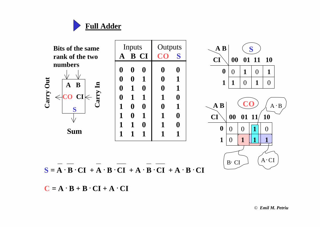
Full Adder
Inputs OutputsA B CI CO S
0 0 0 0 00 0 1 0 10 1 0 0 10 1 1 1 01 0 0 0 11 0 1 1 01 1 0 1 01 1 1 1 1
CI
A B
00 01 11 10
0
1
0 1 0 1
1 0 1 0
S
S = A . B . CI + A . B . CI + A . B . CI + A . B . CI
C = A . B + B . CI + A . CI
B. CI
A . B
A . CI
CI
A B
00 01 11 10
0
1
CO
0 0 1 0
0 1 1 1
© Emil M. Petriu
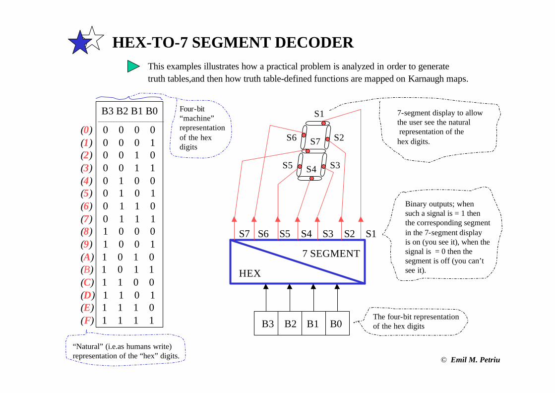
HEX-TO-7 SEGMENT DECODER
B3 B2 B1 B0_________________________
(0) 0 0 0 0(1) 0 0 0 1(2) 0 0 1 0(3) 0 0 1 1(4) 0 1 0 0(5) 0 1 0 1(6) 0 1 1 0(7) 0 1 1 1(8) 1 0 0 0(9) 1 0 0 1(A) 1 0 1 0(B) 1 0 1 1(C) 1 1 0 0(D) 1 1 0 1(E) 1 1 1 0(F) 1 1 1 1
HEX
7 SEGMENT
S7 S6 S5 S4 S3 S2 S1
S1
S2
S3S4
S7S6
S5
B3 B2 B1 B0
This examples illustrates how a practical problem is analyzed in order to generatetruth tables,and then how truth table-defined functions are mapped on Karnaugh maps.
Binary outputs; whensuch a signal is = 1 then the corresponding segmentin the 7-segment display is on (you see it), when thesignal is = 0 then the segment is off (you can’tsee it).
The four-bit representationof the hex digits
7-segment display to allowthe user see the naturalrepresentation of the hex digits.
“Natural” (i.e.as humans write)representation of the “hex” digits.
Four-bit“machine”representationof the hexdigits
© Emil M. Petriu
S1
S2
S3S4
S7S6
S5
S1
S2
S3S4
S7S6
S5
S1
S2
S3S4
S7S6
S5
S1
S2
S3S4
S7S6
S5
S1
S2
S3S4
S7S6
S5
S1
S2
S3S4
S7S6
S5
S1
S2
S3S4
S7S6
S5
S1
S2
S3S4
S7S6
S5
S1
S2
S3S4
S7S6
S5
S1
S2
S3S4
S7S6
S5
S1
S2
S3S4
S7S6
S5
S1
S2
S3S4
S7S6
S5
S1
S2
S3S4
S7S6
S5
S1
S2
S3S4
S7S6
S5
S1
S2
S3S4
S7S6
S5
S1
S2
S3S4
S7S6
S5
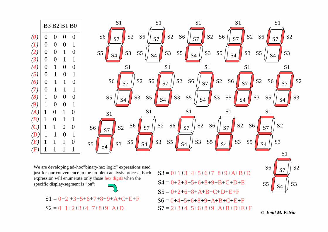
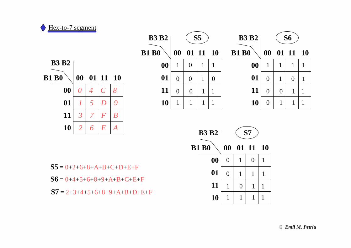
B3 B2 B1 B0_________________________
(0) 0 0 0 0(1) 0 0 0 1(2) 0 0 1 0(3) 0 0 1 1(4) 0 1 0 0(5) 0 1 0 1(6) 0 1 1 0(7) 0 1 1 1(8) 1 0 0 0(9) 1 0 0 1(A) 1 0 1 0(B) 1 0 1 1(C) 1 1 0 0(D) 1 1 0 1(E) 1 1 1 0(F) 1 1 1 1
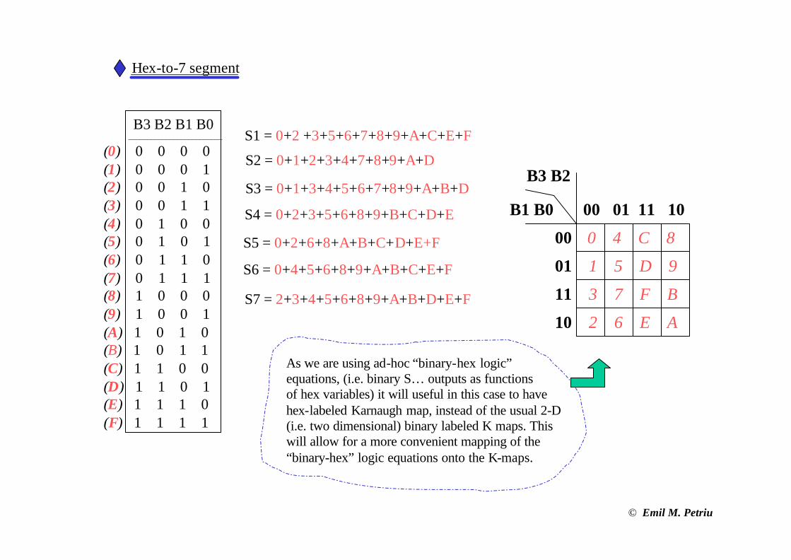
S1 = 0+2 +3+5+6+7+8+9+A+C+E+F
S2 = 0+1+2+3+4+7+8+9+A+D
S3 = 0+1+3+4+5+6+7+8+9+A+B+D
S4 = 0+2+3+5+6+8+9+B+C+D+E
S5 = 0+2+6+8+A+B+C+D+E+FS6 = 0+4+5+6+8+9+A+B+C+E+FS7 = 2+3+4+5+6+8+9+A+B+D+E+F
We are developing ad-hoc”binary-hex logic” expressions used just for our convenience in the problem analysis process. Eachexpression will enumerate only those hex digits when thespecific display-segment is “on”:
© Emil M. Petriu
S1 = 0+2 +3+5+6+7+8+9+A+C+E+F
S2 = 0+1+2+3+4+7+8+9+A+D
S3 = 0+1+3+4+5+6+7+8+9+A+B+D
S4 = 0+2+3+5+6+8+9+B+C+D+E
S5 = 0+2+6+8+A+B+C+D+E+F
S6 = 0+4+5+6+8+9+A+B+C+E+F
S7 = 2+3+4+5+6+8+9+A+B+D+E+F
B3 B2 B1 B0_________________________
(0) 0 0 0 0(1) 0 0 0 1(2) 0 0 1 0(3) 0 0 1 1(4) 0 1 0 0(5) 0 1 0 1(6) 0 1 1 0(7) 0 1 1 1(8) 1 0 0 0(9) 1 0 0 1(A) 1 0 1 0(B) 1 0 1 1(C) 1 1 0 0(D) 1 1 0 1(E) 1 1 1 0(F) 1 1 1 1
B1 B0
B3 B2
00 01 11 10
00 0 4 C 8
1 5 D 9
3 7 F B
2 6 E A
01
11
10
Hex-to-7 segment
As we are using ad-hoc “binary-hex logic”equations, (i.e. binary S… outputs as functionsof hex variables) it will useful in this case to have hex-labeled Karnaugh map, instead of the usual 2-D(i.e. two dimensional) binary labeled K maps. Thiswill allow for a more convenient mapping of the “binary-hex” logic equations onto the K-maps.
© Emil M. Petriu
1 1
1 1
B1 B0
B3 B2
1
10
0
1
11
00 01 11 10
1 10
0
00
01
11
10 1
S1
S1 = 0+2 +3+5+6+7+8+9+A+C+E+F
B1 B0
B3 B2
00 01 11 10
00 0 4 C 8
1 5 D 9
3 7 F B
2 6 E A
01
11
10
S2 = 0+1+2+3+4+7+8+9+A+D
S3 = 0+1+3+4+5+6+7+8+9+A+B+D
S4 = 0+2+3+5+6+8+9+B+C+D+E
0 0
1 0
B1 B0
B3 B2
1
01
1
1
11
00 01 11 10
0 11
0
00
01
11
10 1
S2
1 0
1 0
B1 B0
B3 B2
1
01
1
1
11
00 01 11 10
1 11
1
00
01
11
10 0
S3
1 1
0 0
B1 B0
B3 B2
1
10
0
0
11
00 01 11 10
1 11
1
00
01
11
10 1
S4
Hex-to-7 segment
Mapping the ad-hoc “binary-hex logic” equations onto Karnaugh maps:
© Emil M. Petriu
B1 B0
B3 B2
00 01 11 10
00 0 4 C 8
1 5 D 9
3 7 F B
2 6 E A
01
11
10
1 1
0 1
B1 B0
B3 B2
0
10
0
1
11
00 01 11 10
0 01
1
00
01
11
10 1
S5
1 1
0 1
B1 B0
B3 B2
0
11
0
1
11
00 01 11 10
1 10
1
00
01
11
10 0
S6
1 1
0 1
B1 B0
B3 B2
1
01
0
1
10
00 01 11 10
1 11
1
00
01
11
10 1
S7
S5 = 0+2+6+8+A+B+C+D+E+F
S6 = 0+4+5+6+8+9+A+B+C+E+F
S7 = 2+3+4+5+6+8+9+A+B+D+E+F
Hex-to-7 segment
© Emil M. Petriu
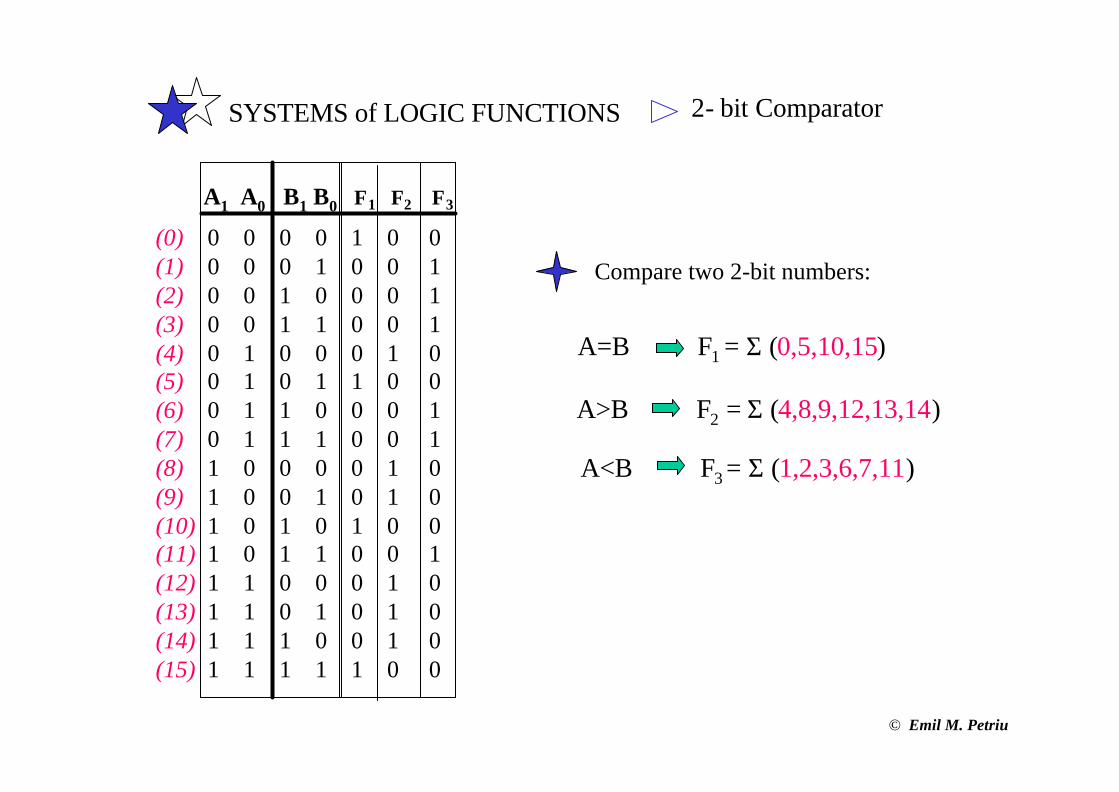
Compare two 2-bit numbers:
A1 A0 B1 B0 F1 F2 F3
(0) 0 0 0 0 1 0 0(1) 0 0 0 1 0 0 1(2) 0 0 1 0 0 0 1(3) 0 0 1 1 0 0 1(4) 0 1 0 0 0 1 0(5) 0 1 0 1 1 0 0(6) 0 1 1 0 0 0 1 (7) 0 1 1 1 0 0 1(8) 1 0 0 0 0 1 0(9) 1 0 0 1 0 1 0(10) 1 0 1 0 1 0 0(11) 1 0 1 1 0 0 1(12) 1 1 0 0 0 1 0(13) 1 1 0 1 0 1 0(14) 1 1 1 0 0 1 0(15) 1 1 1 1 1 0 0
A>B F2 = Σ (4,8,9,12,13,14)
A<B F3 = Σ (1,2,3,6,7,11)
A=B F1 = Σ (0,5,10,15)
2- bit ComparatorSYSTEMS of LOGIC FUNCTIONS
© Emil M. Petriu
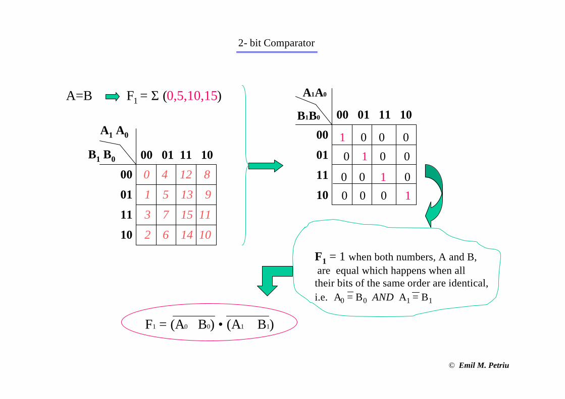
2- bit Comparator
A=B F1 = Σ (0,5,10,15)
0 0 0 1
0 0 1 0
00 01 11 10
00
01
10
1 0 0 0
0 1 0 0
11
A1A0
B1B0
B1 B0
A1 A0
00 01 11 10
00 0 4 12 8
1 5 13 9
3 7 15 11
2 6 14 10
01
11
10
F1 = (A0⊕B0) • (A1 ⊕B1)
F1 = 1 when both numbers, A and B,are equal which happens when alltheir bits of the same order are identical, i.e. A0 = B0 AND A1 = B1
© Emil M. Petriu
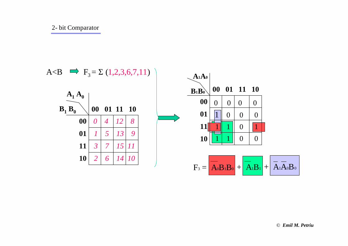
A<B F3 = Σ (1,2,3,6,7,11)
2- bit Comparator
B1 B0
A1 A0
00 01 11 10
00 0 4 12 8
1 5 13 9
3 7 15 11
2 6 14 10
01
11
10+ A1B1 + A1A0B0F3 = A0B1B0
0 0 0 0
1 1 0 1
00 01 11 10
1 0 0 0
1 1 0 0
B1B0
A1A0
01
11
10
00
© Emil M. Petriu
0 0 0 0
0 0 1 0
00 01 11 10
00
01
11
10
0 1 1 1
0 0 1 1
A1A0
B1B0
2- bit Comparator
A>B F2 = Σ (4,8,9,12,13,14) B1 B0
A1 A0
00 01 11 10
00 0 4 12 8
1 5 13 9
3 7 15 11
2 6 14 10
01
11
10
1 0 0 0
1 1 1 1
00 01 11 10
1 1 0 0
1 1 0 1
B1B0
A1A0
01
11
10
00
F1+F3
F2 = F1 + F3
0 0 0 0
1 1 0 1
00 01 11 10
1 0 0 0
1 1 0 0
B1B0
A1A0
01
11
10
00
F3
0 0 0 1
0 0 1 0
00 01 11 10
00
01
10
1 0 0 0
0 1 0 0
11
A1A0
B1B0
F1
© Emil M. Petriu
B1 B0 A1 A0
A0 ⊕B0
A1 ⊕B1
F1 = (A0⊕B0) • (A1 ⊕B1)
F2 = F1 + F3
F3 = A0B1B0+A1B1+A1A0B0
2- bit Comparator
F2 = F1 + F3
F3 = A0B1B0+A1B1+A1A0B0
F1 = (A0⊕B0) • (A1 ⊕B1)
© Emil M. Petriu
A B C F0 F1 F2 F3 F4 F5 F6 F7
(0) 0 0 0 1 0 0 0 0 0 0 0 (1) 0 0 1 0 1 0 0 0 0 0 0 (2) 0 1 0 0 0 1 0 0 0 0 0 (3) 0 1 1 0 0 0 1 0 0 0 0 (4) 1 0 0 0 0 0 0 1 0 0 0 (5) 1 0 1 0 0 0 0 0 1 0 0 (6) 1 1 0 0 0 0 0 0 0 1 0 (7) 1 1 1 0 0 0 0 0 0 0 1
F0
F2
F3
F1
F4
F5
F6
F7
A B C3-to-8 Decoder
© Emil M. Petriu
F0
F2
F3
F1
F4
F5
F6
F7
A B C E F0 F1 F2 F3 F4 F5 F6 F7
(x) x x x 1 1 1 1 1 1 1 1 1(0) 0 0 0 0 0 1 1 1 1 1 1 1(1) 0 0 1 0 1 0 1 1 1 1 1 1(2) 0 1 0 0 1 1 0 1 1 1 1 1(3) 0 1 1 0 1 1 1 0 1 1 1 1(4) 1 0 0 0 1 1 1 1 0 1 1 1(5) 1 0 1 0 1 1 1 1 1 0 1 1(6) 1 1 0 0 1 1 1 1 1 1 0 1(7) 1 1 1 0 1 1 1 1 1 1 1 0
E A B C3-to-8 Decoder (74 138)
© Emil M. Petriu
BCD-TO-7 SEGMENT DECODER
B3 B2 B1 B0_________________________
(0) 0 0 0 0(1) 0 0 0 1(2) 0 0 1 0(3) 0 0 1 1(4) 0 1 0 0(5) 0 1 0 1(6) 0 1 1 0(7) 0 1 1 1(8) 1 0 0 0(9) 1 0 0 1(x) 1 0 1 0(x) 1 0 1 1(x) 1 1 0 0(x) 1 1 0 1(x) 1 1 1 0(x) 1 1 1 1
BCD
7 SEGMENT
S7 S6 S5 S4 S3 S2 S1
S1
S2
S3S4
S7S6
S5
B3 B2 B1 B0
B1 B0
B3 B2
00 01 11 10
00 0 4 x 8
1 5 x 9
3 7 x x
2 6 x x
01
11
10
“Don’t Care” states/situations.As it is expected that thesestates are never going to occur,then we may just as well use them as fill-in “1s” in a Karnaugh map if this helps to make larger loopings
© Emil M. Petriu
S1
S2
S3S4
S7S6
S5
S1
S2
S3S4
S7S6
S5
S1
S2
S3S4
S7S6
S5
S1
S2
S3S4
S7S6
S5
S1
S2
S3S4
S7S6
S5
S1
S2
S3S4
S7S6
S5
S1
S2
S3S4
S7S6
S5
S1
S2
S3S4
S7S6
S5
S1
S2
S3S4
S7S6
S5
S1
S2
S3S4
S7S6
S5
B3 B2 B1 B0_________________________
(0) 0 0 0 0(1) 0 0 0 1(2) 0 0 1 0(3) 0 0 1 1(4) 0 1 0 0(5) 0 1 0 1(6) 0 1 1 0(7) 0 1 1 1(8) 1 0 0 0(9) 1 0 0 1(x) 1 0 1 0(x) 1 0 1 1(x) 1 1 0 0(x) 1 1 0 1(x) 1 1 1 0(x) 1 1 1 1
S1 = 0+2 +3+5+6+7+8+9
S2 = 0+1+2+3+4+7+8+9
S3 = 0+1+3+4+5+6+7+8+9
S4 = 0+2+3+5+6+8+9
S5 = 0+2+6+8
S6 = 0+4+5+6+8+9
S7 = 2+3+4+5+6+8+9
BCD-to-7 segment
© Emil M. Petriu
1 x1 x
1 x
B1 B0
B3 B2
x0
0
x
11
00 01 11 10
1 1x
00
01
11
10 1
S1
10
00 01 11 10B1 B0
0
1
B3 B2
1
1
1
1
0 1
00
01
11
1 x
x
x
x
x
x
S2
1
B3S2 = + B2 + B1B0 + B1B0
S1 = 0+2 +3+5+6+7+8+9
S2 = 0+1+2+3+4+7+8+9
B1 B0
B3 B2
00 01 11 10
00 0 4 x 8
1 5 x 9
3 7 x x
2 6 x x
01
11
10
BCD-to-7 segment
S1 = B3 +
B2B0++ B2B1
+ B2B0 B1
© Emil M. Petriu
1
1
B1 B0B3 B2
1
1
1
11
00 01 11 10
1 1
00
01
11
10 0
S3
x
x
x
x
x
x
S3 = + B1B0 + B2B3 + B1
S3 = 0+1+3+4+5+6+7+8+9
1
0
B1 B0
B3 B2
1
0
0
11
00 01 11 10
1 1
00
01
11
10 1
S4
x
x
x
x
x
x
B1B0S4 = B2B1B0+ ++ B2B0B3 + B2B1
S4 = 0+2+3+5+6+8+9
B1 B0
B3 B2
00 01 11 10
00 0 4 x 8
1 5 x 9
3 7 x x
2 6 x x
01
11
10
BCD-to-7 segment
© Emil M. Petriu
B1 B0
1
0
B3 B2
0
0
0
11
00 01 11 10
0 0
00
01
11
10 1
S5
x
x
x
x
x
x
B1B0S5 = +B2B0 B2B0B1B2B3 +S6 = + B1B0 +
B1B0B1B2
B2B1
+
S7 = B3 +
+
S6 = 0+4+5+6+8+9S5 = 0+2+6+8
S7 = 2+3+4+5+6+8+9
B1 B0
B3 B2
00 01 11 10
00 0 4 x 8
1 5 x 9
3 7 x x
2 6 x x
01
11
10
BCD-to-7 segment
1
00
1
0
11
00 01 11 10
1 1
00
01
11
10 0
S6
x
x
x
x
x
x
B1 B0
B3 B2
B1 B0
B3 B2
01
1
0
10
00 01 11 10
1 1
00
01
11
10
S7
x
x
x
x11 x x
© Emil M. Petriu
MEMORY ELEMENTS: LATCHES AND FLIP-FLOPS
QS
RQ
R-S Latch(Reset-Set)
S R Q Q
0 0 1 10 1 1 01 0 0 11 1 Q Q
Weird stateSet state
Reset stateHold state
I1
I2
F
I1 I2 F
0 0 10 1 11 0 11 1 0
S Q
R Q= 1
= 1S Q
R Q= 0
= 1
= 1
S Q
R Q= 1
= 0 = 1
S Q
R Q= 0
= 0 = 1
= 1
= 0
= 0
= 0
= 1
© Emil M. Petriu
D (Transparent) Latch
QS
R
Q
D
Enable
S R Q Q
0 0 1 10 1 1 01 0 0 11 1 Q Q
Enable D S R Q Q
Q Q
Q Q
0 11 0
0 0 1 1
0 1 1 1
1 0 1 01 1 0 1
When the Enable inputis =1 (i.e. TRUE or HIGH)the information present at the D input is stored in the latch and will “appear as it is” at the Q output ( => it is likethat there is a “transparent” path from the D input to the Q output)
Enable D Q Q
Q Q
0 11 0
0 x
1 01 1
© Emil M. Petriu
D Latch
QS
R
Q
D
Enable
Enable D S R Q Q
Q Q
Q Q
0 11 0
0 0 1 1
0 1 1 1
1 0 1 01 1 0 1
Enable1
01
01
01
01
0
D
S
Q
R
Hold
“Hold”state “Hold”state“Transparent” state
© Emil M. Petriu
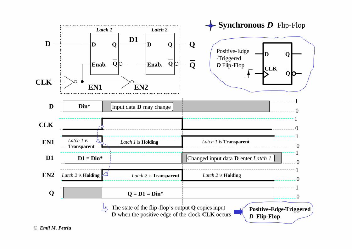
Synchronous D Flip-Flop
D
CLK
Q
Q
D1
EN1 EN2
Q
Q
D
Enab.
Q
Q
D
Enab.
Latch 1 Latch 2
1
01
01
01
01
01
0
D
CLK
EN1
EN2
D1
Q
Latch 2 is Transparent Latch 2 is HoldingLatch 2 is Holding
Latch 1 is TransparentLatch 1 is HoldingLatch 1 isTransparent
D1 = Din*
Din*
Q = D1 = Din*
Input data D may change
Changed input data D enter Latch 1
The state of the flip-flop’s output Q copies input D when the positive edge of the clock CLK occurs
Positive-Edge-Triggered D Flip-Flop
Q
Q
D
CLK
Positive-Edge-TriggeredD Flip-Flop
© Emil M. Petriu
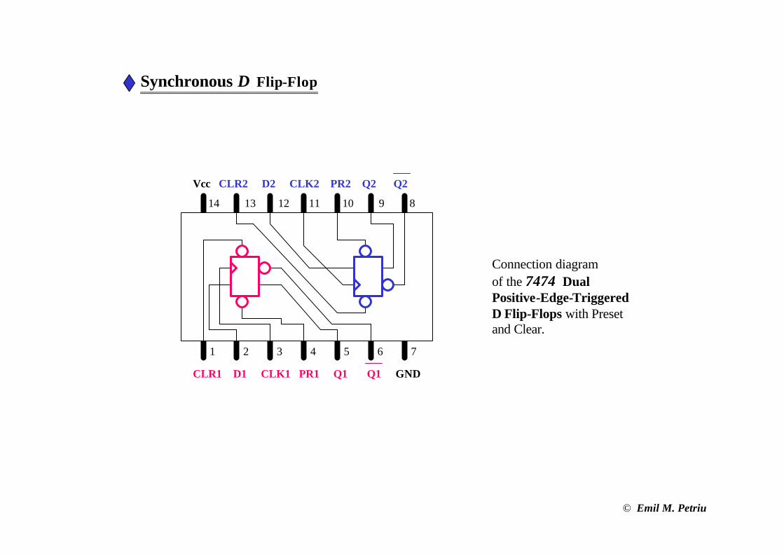
Connection diagramof the 7474 Dual Positive-Edge-Triggered D Flip-Flops with Preset and Clear.
CLR1 D1 CLK1 PR1 Q1 Q1 GND
1 2 3 4 5 6 7
14 13 12 11 10 9 8
Vcc CLR2 D2 CLK2 PR2 Q2 Q2
Synchronous D Flip-Flop
© Emil M. Petriu
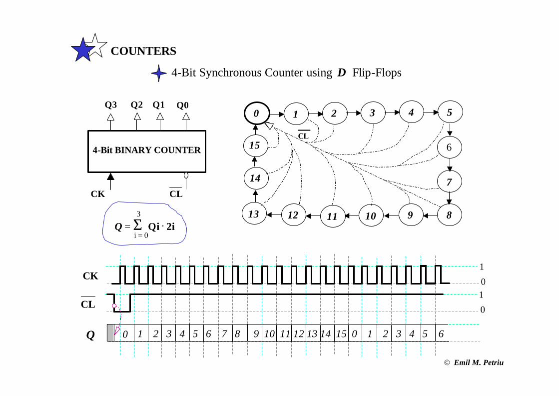
COUNTERS
4-Bit Synchronous Counter using D Flip-Flops
Q = Σ Qi . 2ii = 0
3
0 1 2 3 4 5
10 9 8111213
6
7
15
14
Q3 Q1 Q0Q2
CK
4-Bit BINARY COUNTER
CL
1
0CK
Q 0 1 2 3 4 5 6 7 8 9 10 11 12 13 14 15 0 1 2 3 4 5 6
CL
1
0CL
© Emil M. Petriu
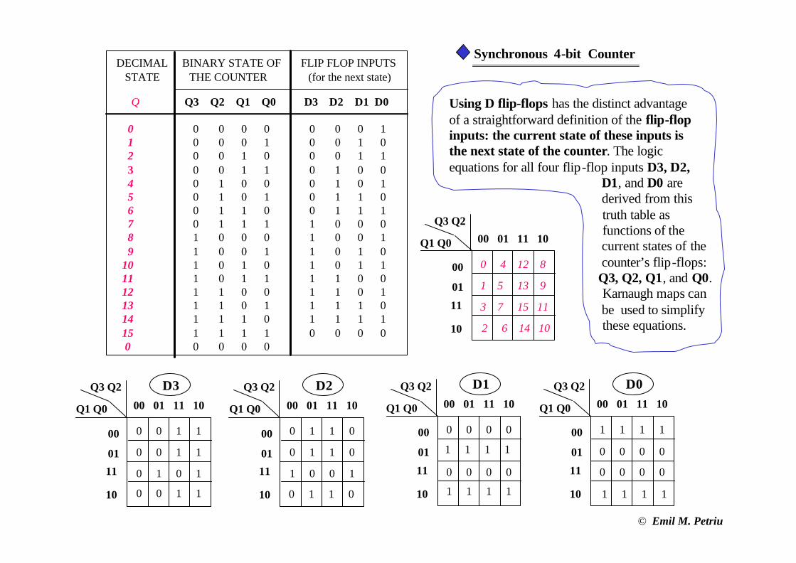
DECIMAL BINARY STATE OF FLIP FLOP INPUTSSTATE THE COUNTER (for the next state)
Q Q3 Q2 Q1 Q0 D3 D2 D1 D0
0 0 0 0 0 0 0 0 11 0 0 0 1 0 0 1 02 0 0 1 0 0 0 1 13 0 0 1 1 0 1 0 04 0 1 0 0 0 1 0 15 0 1 0 1 0 1 1 06 0 1 1 0 0 1 1 17 0 1 1 1 1 0 0 08 1 0 0 0 1 0 0 19 1 0 0 1 1 0 1 0
10 1 0 1 0 1 0 1 111 1 0 1 1 1 1 0 0 12 1 1 0 0 1 1 0 113 1 1 0 1 1 1 1 014 1 1 1 0 1 1 1 115 1 1 1 1 0 0 0 00 0 0 0 0
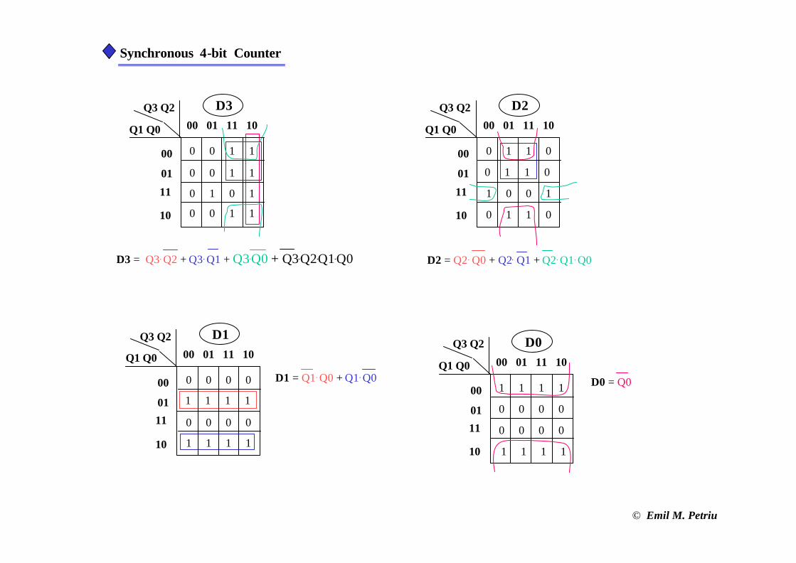
Using D flip-flops has the distinct advantage of a straightforward definition of the flip-flop inputs: the current state of these inputs is the next state of the counter. The logic equations for all four flip-flop inputs D3, D2,
D1, and D0 are derived from this truth table as functions of the current states of thecounter’s flip-flops:
Q3, Q2, Q1, and Q0. Karnaugh maps can be used to simplify these equations.
Q1 Q0
Q3 Q2
00 01 11 10
00 0 1 1 0
0 1 1 0
1 0 0 1
0 1 1 0
01
11
10
D2
Q1 Q0
Q3 Q2
00 01 11 10
00 0 0 1 1
0 0 1 1
0 1 0 1
0 0 1 1
01
11
10
D3
Q1 Q0
Q3 Q2
00 01 11 10
00 0 0 0 0
1 1 1 1
0 0 0 0
1 1 1 1
01
11
10
D1
Q1 Q0
Q3 Q2
00 01 11 10
00 1 1 1 1
0 0 0 0
0 0 0 0
1 1 1 1
01
11
10
D0
Synchronous 4-bit Counter
Q1 Q0
Q3 Q2
00 01 11 10
00 0 4 12 8
1 5 13 9
3 7 15 11
2 6 14 10
01
11
10
© Emil M. Petriu
Synchronous 4-bit Counter
Q1 Q0
Q3 Q2
00 01 11 10
00
0 1 1 0
1 0 0 1
01
11
10
D2
0 1 1 0
0 1 1 0
Q1 Q0
Q3 Q2
00 01 11 10
00 0 0 0 0
0 0 0 0
01
11
10
D1
1 1 1 1
1 1 1 1
D3 = Q3. Q2 + Q3. Q1 + Q3.Q0 + Q3.Q2.Q1.Q0 D2 = Q2. Q0 + Q2. Q1 + Q2. Q1. Q0
D1 = Q1. Q0 + Q1. Q0 D0 = Q0Q1 Q0
Q3 Q2
00 01 11 10
00 1 1 1 1
0 0 0 0
0 0 0 0
1 1 1 1
01
11
10
D0
Q1 Q0
Q3 Q2
00 01 11 10
00
01
11
10
D3
0 0 1 1
0 0 1 1
0 1 0 1
0 0 1 1
© Emil M. Petriu
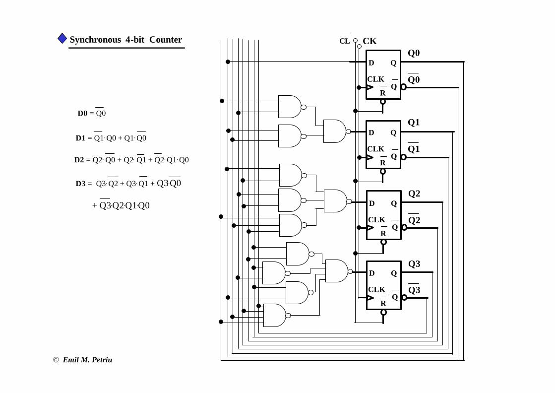
D3 = Q3. Q2 + Q3. Q1 + Q3.Q0
+ Q3.Q2.Q1.Q0
D2 = Q2. Q0 + Q2. Q1 + Q2. Q1. Q0
D1 = Q1. Q0 + Q1. Q0
D0 = Q0
Synchronous 4-bit Counter
D
CLK
Q
QR
Q0
Q0
D
CLK
Q
QR
Q1
Q1
D
CLK
Q
QR
Q2
Q2
D
CLK
Q
QR
Q3
Q3
CL CK
© Emil M. Petriu