Embed Size (px)
Citation preview
Adib AbrishamifarEE Department
IUST
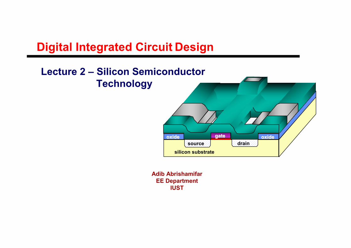
Lecture 2 – Silicon Semiconductor Technology
Digital Integrated Circuit Design
silicon substratesource drain
gategateoxideoxide oxideoxide
IUST: Digital IC Design LECTURE 2 : TechnologyLECTURE 2 : Technology Adib Abrishamifar 20082/161
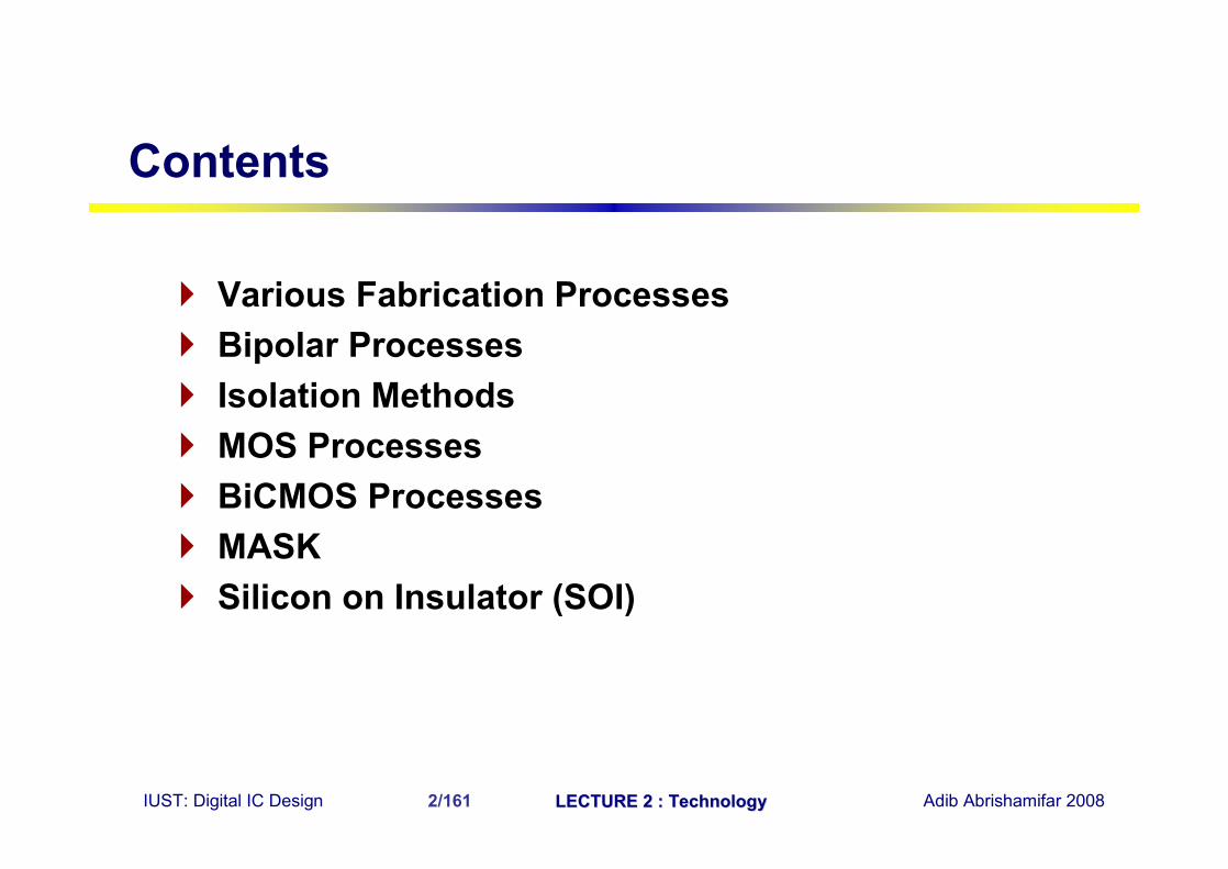
Various Fabrication Processes Bipolar Processes Isolation Methods MOS Processes BiCMOS Processes MASK Silicon on Insulator (SOI)
Contents
IUST: Digital IC Design LECTURE 2 : TechnologyLECTURE 2 : Technology Adib Abrishamifar 20083/161
Various Fabrication Processes
Planarization (Polishing the Wafers) Photolithography Oxide Growth Etching Doping (Diffusion, Ion Implantation) Metallisation
IUST: Digital IC Design LECTURE 2 : TechnologyLECTURE 2 : Technology Adib Abrishamifar 20084/161
Planarization
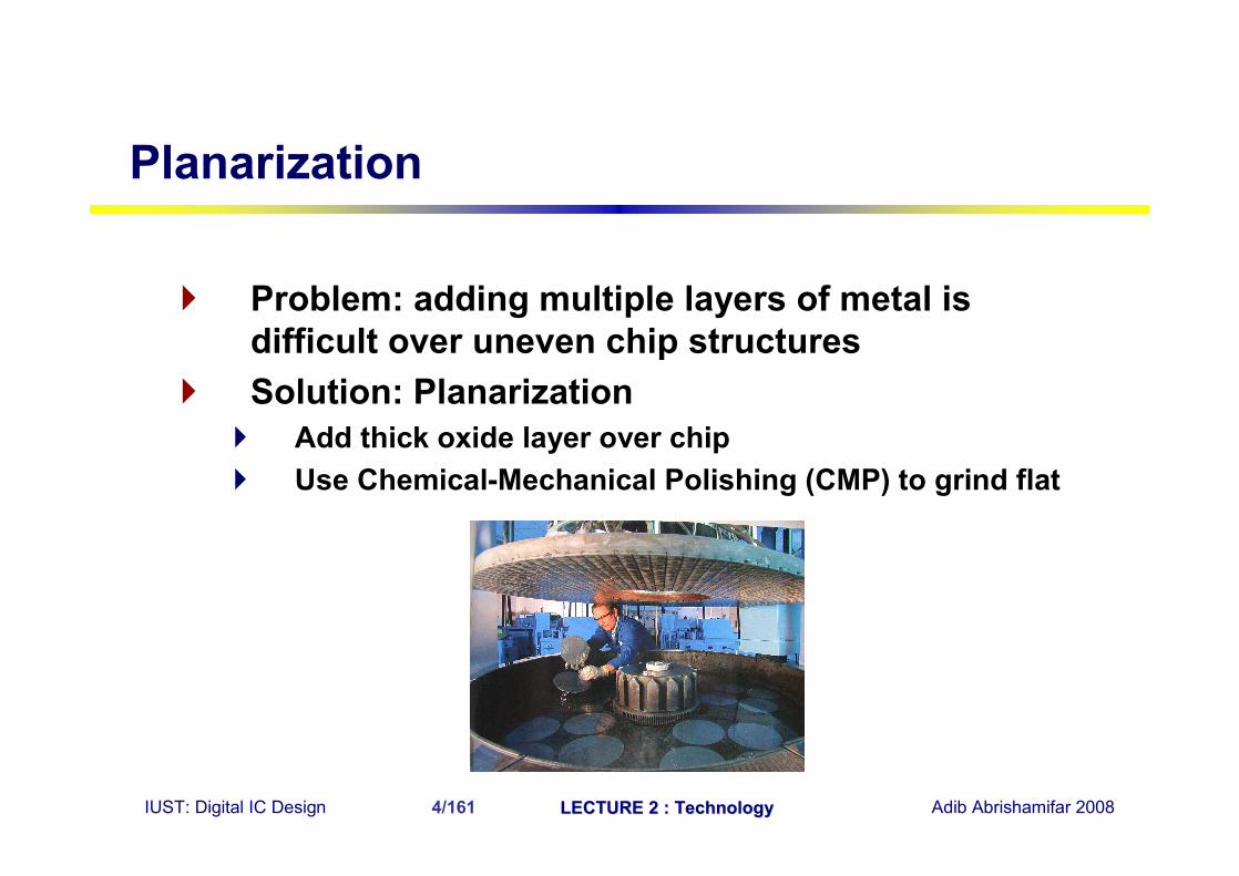
Problem: adding multiple layers of metal is difficult over uneven chip structures
Solution: Planarization Add thick oxide layer over chip Use Chemical-Mechanical Polishing (CMP) to grind flat
IUST: Digital IC Design LECTURE 2 : TechnologyLECTURE 2 : Technology Adib Abrishamifar 20085/161
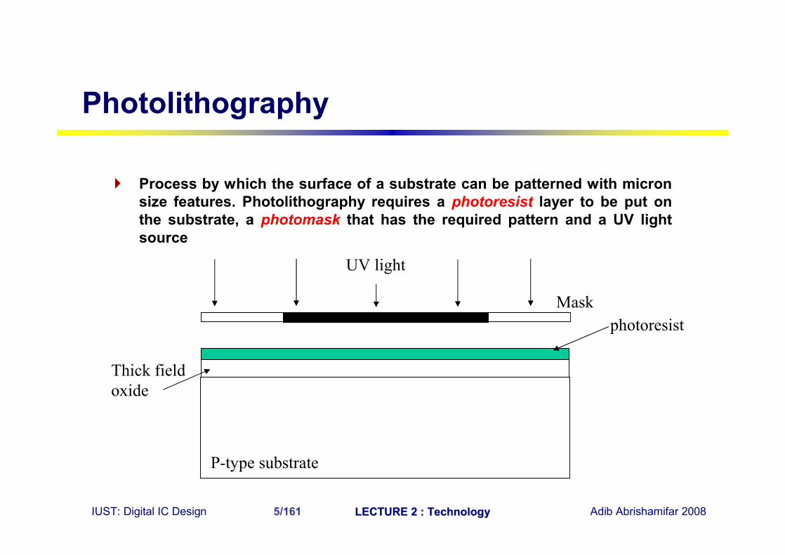
Process by which the surface of a substrate can be patterned with micronsize features. Photolithography requires a photoresist layer to be put on the substrate, a photomask that has the required pattern and a UV light source
Photolithography
P-type substrate
Thick field oxide
photoresist
UV light
Mask
IUST: Digital IC Design LECTURE 2 : TechnologyLECTURE 2 : Technology Adib Abrishamifar 20086/161
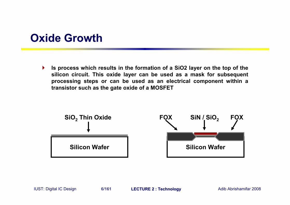
Is process which results in the formation of a SiO2 layer on the top of thesilicon circuit. This oxide layer can be used as a mask for subsequent processing steps or can be used as an electrical component within a transistor such as the gate oxide of a MOSFET
Oxide Growth
Silicon Wafer Silicon Wafer
SiN / SiO2FOX FOXSiO2 Thin Oxide
IUST: Digital IC Design LECTURE 2 : TechnologyLECTURE 2 : Technology Adib Abrishamifar 20087/161
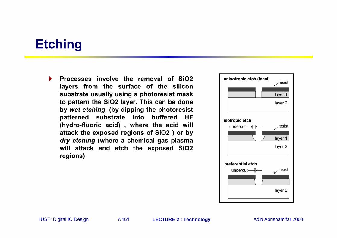
Processes involve the removal of SiO2 layers from the surface of the siliconsubstrate usually using a photoresist mask to pattern the SiO2 layer. This can be done by wet etching, (by dipping the photoresistpatterned substrate into buffered HF(hydro-fluoric acid) , where the acid willattack the exposed regions of SiO2 ) or by dry etching (where a chemical gas plasma will attack and etch the exposed SiO2 regions)
Etching
anisotropic etch (ideal)resist
layer 1
layer 2
resist
layer 1
layer 2
isotropic etchundercut
resist
layer 1
layer 2
preferential etchundercut
IUST: Digital IC Design LECTURE 2 : TechnologyLECTURE 2 : Technology Adib Abrishamifar 20088/161
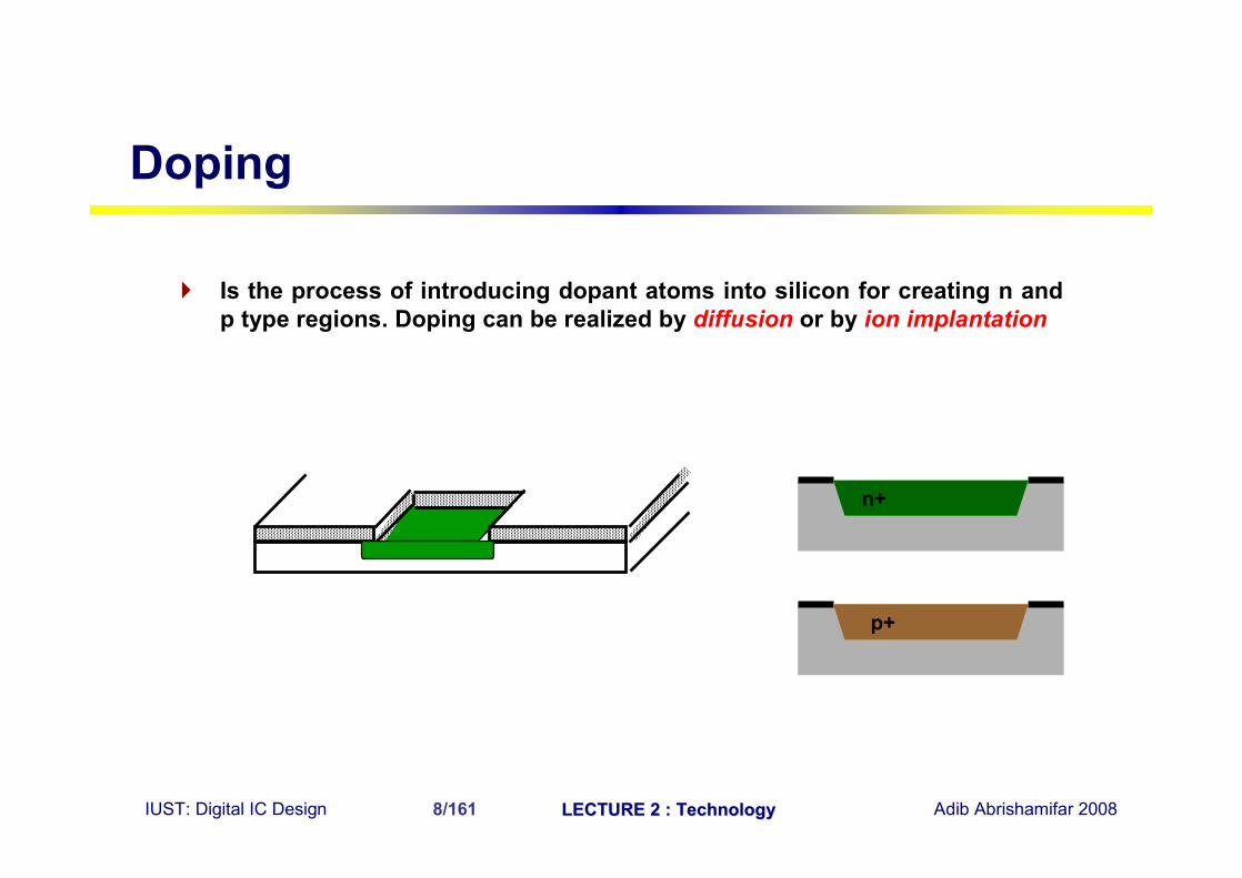
Is the process of introducing dopant atoms into silicon for creating n and p type regions. Doping can be realized by diffusion or by ion implantation
Doping
nn+
pp+
IUST: Digital IC Design LECTURE 2 : TechnologyLECTURE 2 : Technology Adib Abrishamifar 20089/161
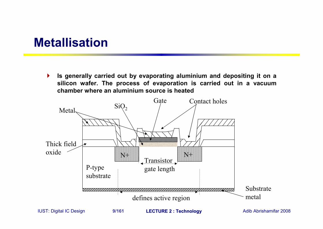
Is generally carried out by evaporating aluminium and depositing it on asilicon wafer. The process of evaporation is carried out in a vacuum chamber where an aluminium source is heated
Metallisation
Thick field oxide
P-type substrate
N+ N+
GateSiO2
Contact holesMetal
Transistor gate length
Substrate metaldefines active region
IUST: Digital IC Design LECTURE 2 : TechnologyLECTURE 2 : Technology Adib Abrishamifar 200810/161
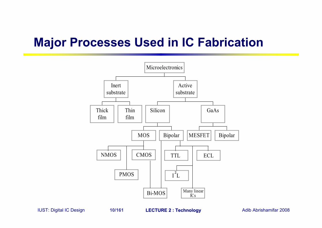
NMOS CMOS TTL ECL
PMOS
Bi-MOS Many linearICs
2I L
Thickfilm
Thinfilm
Inertsubstrate
MOS Bipolar
Silicon
MESFET Bipolar
GaAs
Activesubstrate
Microelectronics
Major Processes Used in IC Fabrication
IUST: Digital IC Design LECTURE 2 : TechnologyLECTURE 2 : Technology Adib Abrishamifar 200811/161
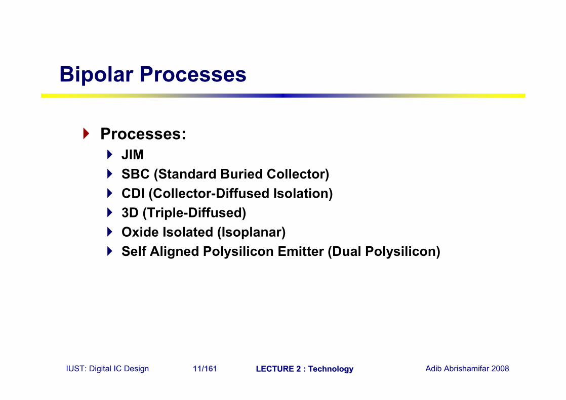
Bipolar Processes
Processes: JIM SBC (Standard Buried Collector) CDI (Collector-Diffused Isolation) 3D (Triple-Diffused) Oxide Isolated (Isoplanar) Self Aligned Polysilicon Emitter (Dual Polysilicon)
IUST: Digital IC Design LECTURE 2 : TechnologyLECTURE 2 : Technology Adib Abrishamifar 200812/161
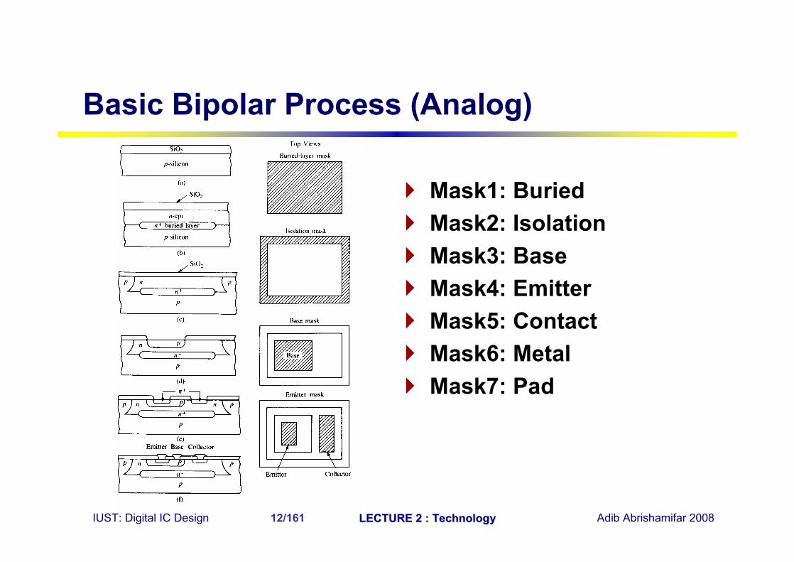
Basic Bipolar Process (Analog)
Mask1: Buried Mask2: Isolation Mask3: Base Mask4: Emitter Mask5: Contact Mask6: Metal Mask7: Pad
IUST: Digital IC Design LECTURE 2 : TechnologyLECTURE 2 : Technology Adib Abrishamifar 200813/161
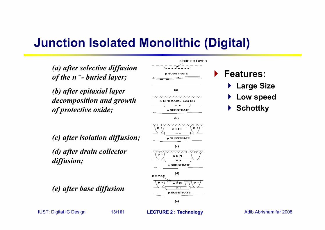
(a) after selective diffusion of the n +- buried layer;
(b) after epitaxial layer decomposition and growth of protective oxide;
(c) after isolation diffusion;
(d) after drain collector diffusion;
(e) after base diffusion
Junction Isolated Monolithic (Digital)
Features: Large Size Low speed Schottky
IUST: Digital IC Design LECTURE 2 : TechnologyLECTURE 2 : Technology Adib Abrishamifar 200814/161
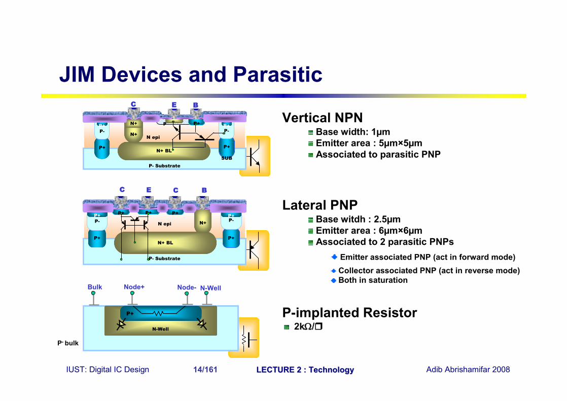
P- bulk
C E B
Vertical NPNBase width: 1µmEmitter area : 5µm×5µmAssociated to parasitic PNP
Node+ Node-Bulk N-Well
N-Well
P+
C E
N+N epi
P+P+P+
P- Substrate
P+P+
P-P+
P-P+
N+
N+ BL
C BC C CC Lateral PNP
Base witdh : 2.5µmEmitter area : 6µm×6µmAssociated to 2 parasitic PNPs
Emitter associated PNP (act in forward mode)Collector associated PNP (act in reverse mode)Both in saturation
P-implanted Resistor2kΩ/r
N epi
P- Substrate
P+
SUB
P+
P
N+
N+ P+P-P+
P-P+
N+ BL
C C C
JIM Devices and Parasitic
IUST: Digital IC Design LECTURE 2 : TechnologyLECTURE 2 : Technology Adib Abrishamifar 200815/161
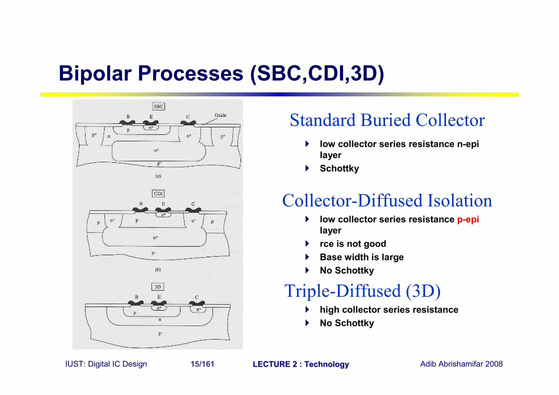
Standard Buried Collector
Triple-Diffused (3D)
Collector-Diffused Isolation
Bipolar Processes (SBC,CDI,3D)
low collector series resistance n-epilayer
Schottky
low collector series resistance p-epilayer
rce is not good Base width is large No Schottky
high collector series resistance No Schottky
IUST: Digital IC Design LECTURE 2 : TechnologyLECTURE 2 : Technology Adib Abrishamifar 200816/161
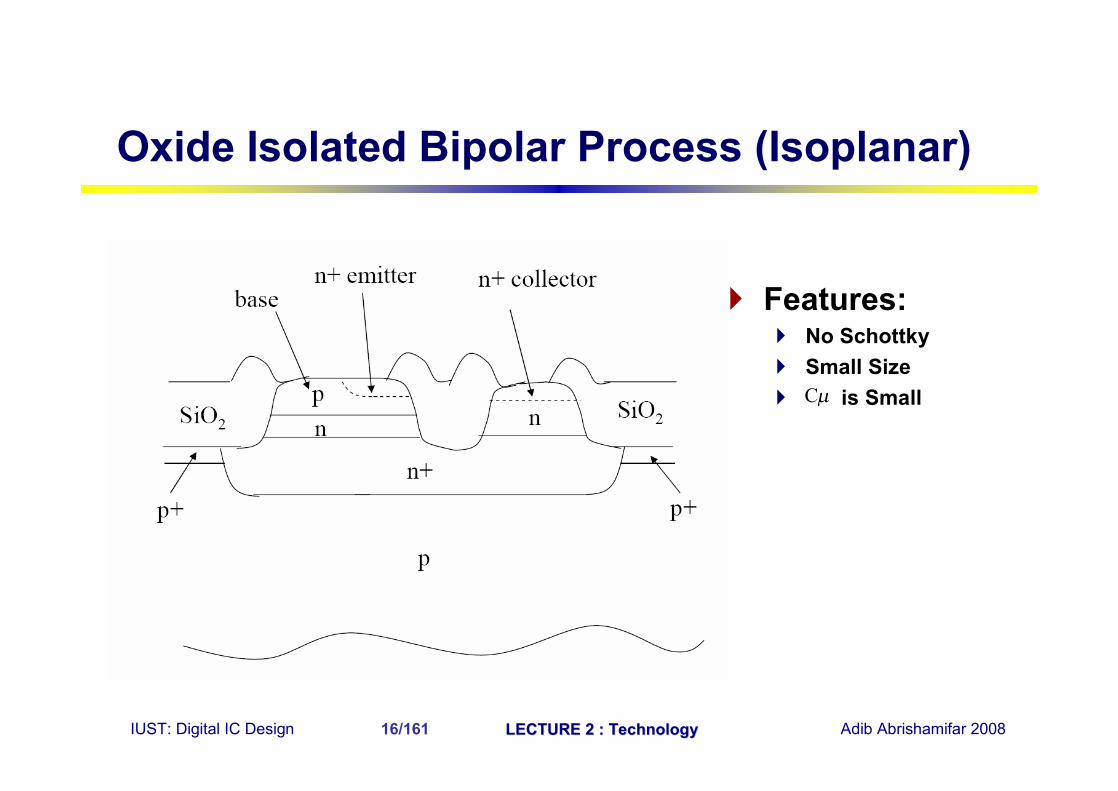
Oxide Isolated Bipolar Process (Isoplanar)
Features: No Schottky Small Size is SmallC µ
IUST: Digital IC Design LECTURE 2 : TechnologyLECTURE 2 : Technology Adib Abrishamifar 200817/161
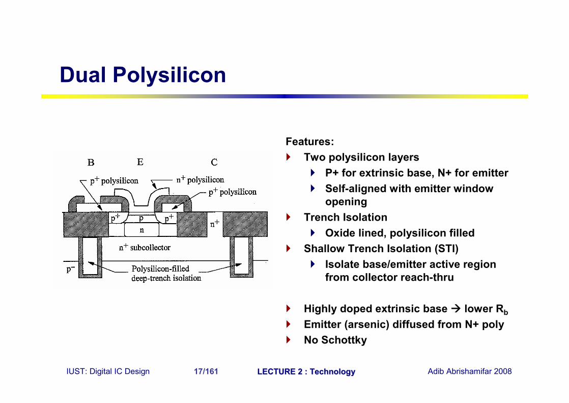
Features: Two polysilicon layers
P+ for extrinsic base, N+ for emitter Self-aligned with emitter window
opening Trench Isolation
Oxide lined, polysilicon filled Shallow Trench Isolation (STI)
Isolate base/emitter active region from collector reach-thru
Highly doped extrinsic base à lower Rb
Emitter (arsenic) diffused from N+ poly No Schottky
Dual Polysilicon
IUST: Digital IC Design LECTURE 2 : TechnologyLECTURE 2 : Technology Adib Abrishamifar 200818/161
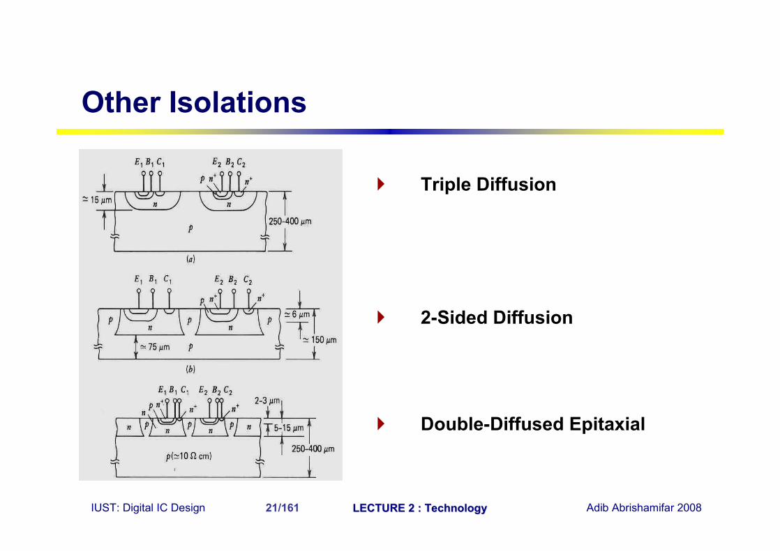
Isolation Methods
Isolations: Lateral Triple Diffusion 2-Sided Diffusion (Double-Diffused Epitaxial) Oxide Isolated
IUST: Digital IC Design LECTURE 2 : TechnologyLECTURE 2 : Technology Adib Abrishamifar 200819/161
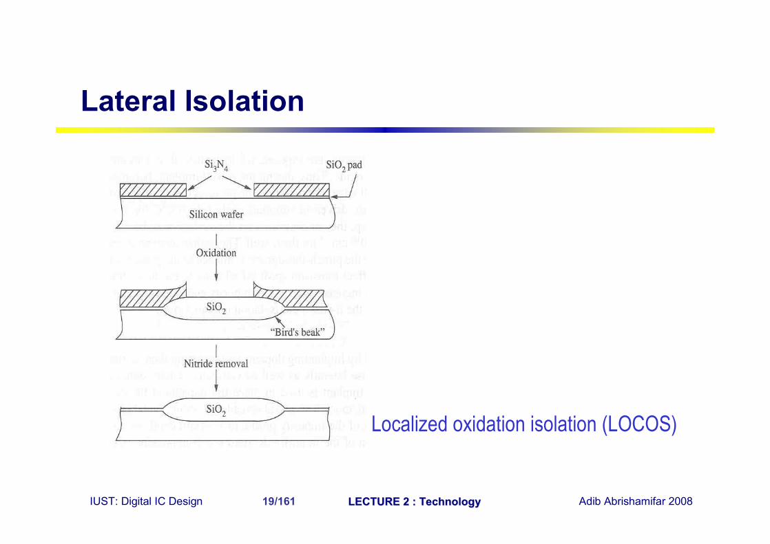
Localized oxidation isolation (LOCOS)
Lateral Isolation
IUST: Digital IC Design LECTURE 2 : TechnologyLECTURE 2 : Technology Adib Abrishamifar 200820/161
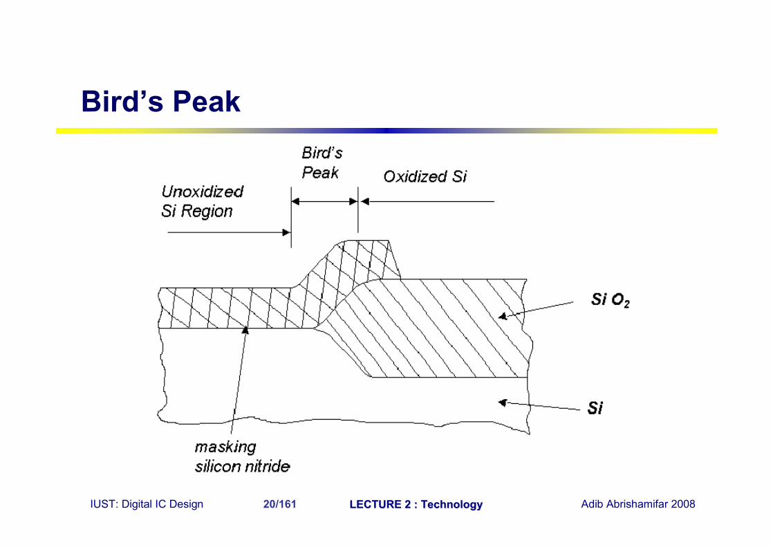
Bird’s Peak
IUST: Digital IC Design LECTURE 2 : TechnologyLECTURE 2 : Technology Adib Abrishamifar 200821/161
Other Isolations
Triple Diffusion
2-Sided Diffusion
Double-Diffused Epitaxial
IUST: Digital IC Design LECTURE 2 : TechnologyLECTURE 2 : Technology Adib Abrishamifar 200822/161
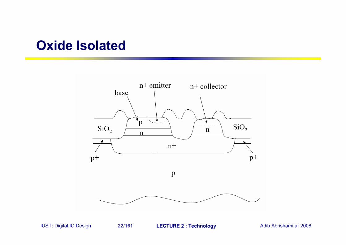
Oxide Isolated
IUST: Digital IC Design LECTURE 2 : TechnologyLECTURE 2 : Technology Adib Abrishamifar 200823/161
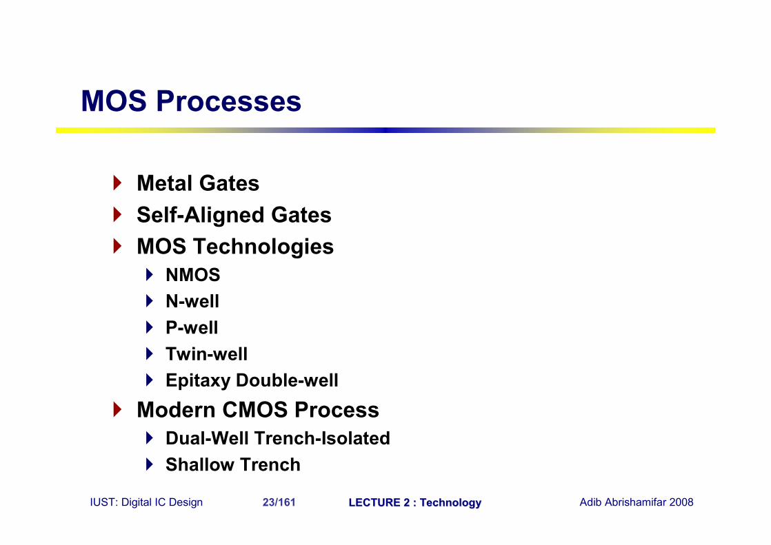
MOS Processes
Metal Gates Self-Aligned Gates MOS Technologies NMOS N-well P-well Twin-well Epitaxy Double-well
Modern CMOS Process Dual-Well Trench-Isolated Shallow Trench
IUST: Digital IC Design LECTURE 2 : TechnologyLECTURE 2 : Technology Adib Abrishamifar 200824/161
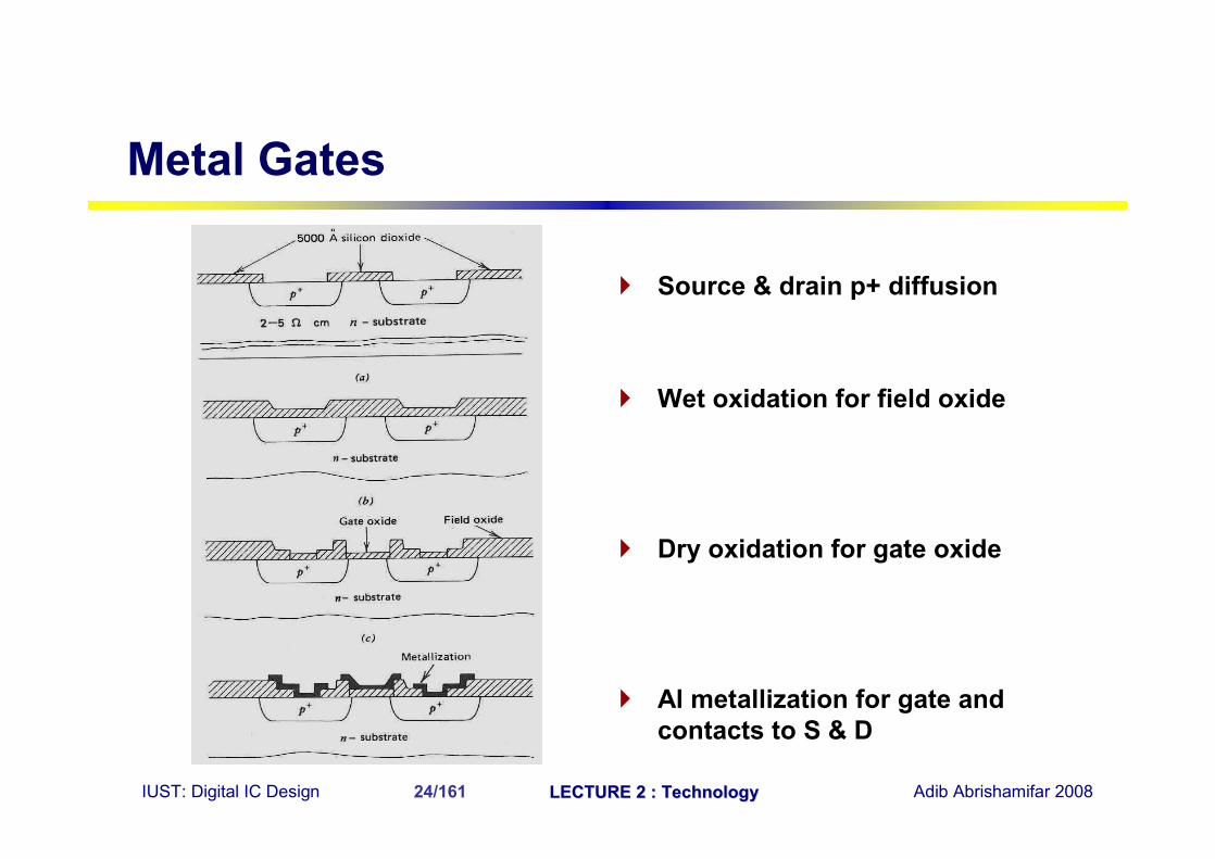
Source & drain p+ diffusion
Wet oxidation for field oxide
Dry oxidation for gate oxide
Al metallization for gate and contacts to S & D
Metal Gates
IUST: Digital IC Design LECTURE 2 : TechnologyLECTURE 2 : Technology Adib Abrishamifar 200825/161
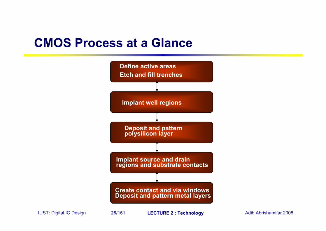
Define active areasEtch and fill trenches
Implant well regions
Deposit and patternpolysilicon layer
Implant source and drainregions and substrate contacts
Create contact and via windowsDeposit and pattern metal layers
CMOS Process at a Glance
IUST: Digital IC Design LECTURE 2 : TechnologyLECTURE 2 : Technology Adib Abrishamifar 200826/161
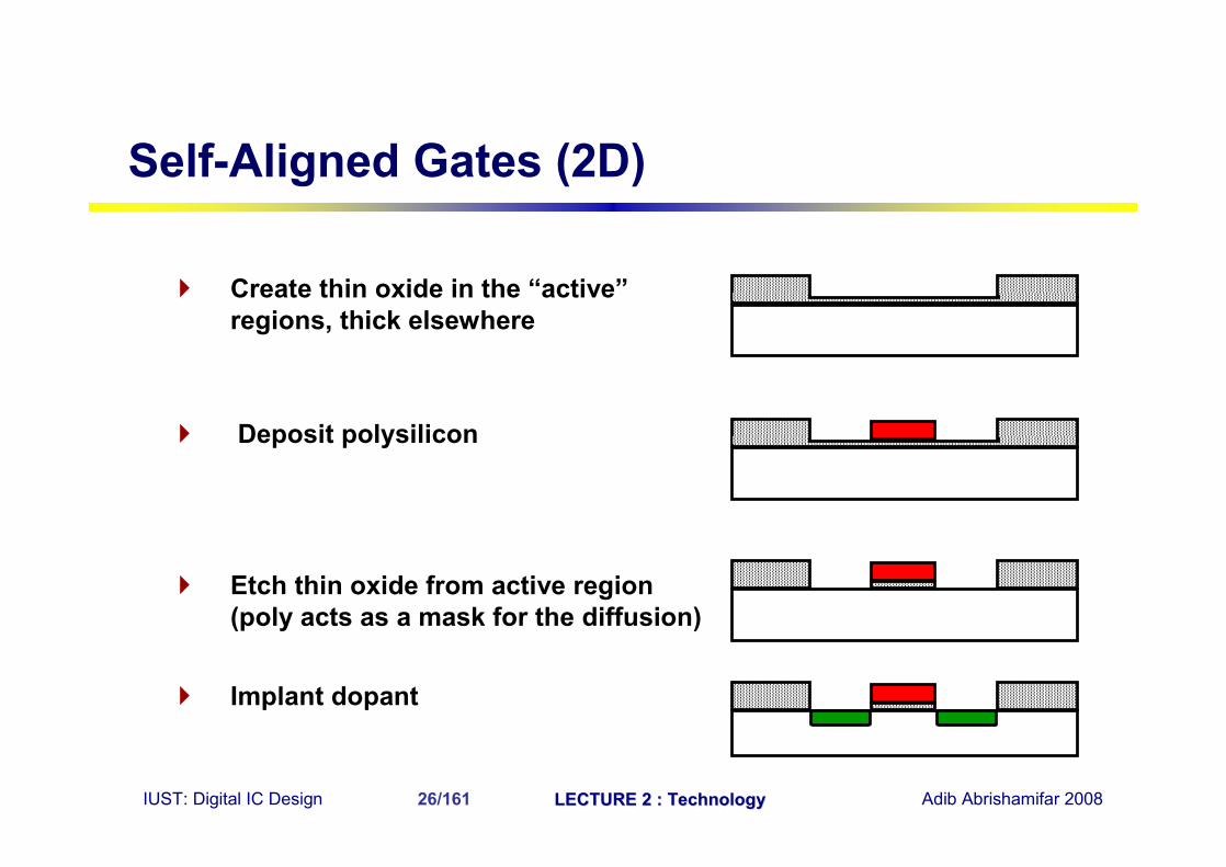
Self-Aligned Gates (2D)
Create thin oxide in the “active”regions, thick elsewhere
Deposit polysilicon
Etch thin oxide from active region (poly acts as a mask for the diffusion)
Implant dopant
IUST: Digital IC Design LECTURE 2 : TechnologyLECTURE 2 : Technology Adib Abrishamifar 200827/161
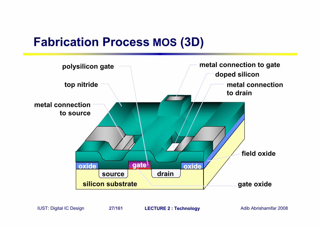
silicon substratesource drain
gategateoxideoxide oxideoxide
top nitride
metal connection to source
metal connection to gate
metal connection to drain
polysilicon gatedoped silicon
field oxide
gate oxide
Fabrication Process MOS (3D)
IUST: Digital IC Design LECTURE 2 : TechnologyLECTURE 2 : Technology Adib Abrishamifar 200828/161
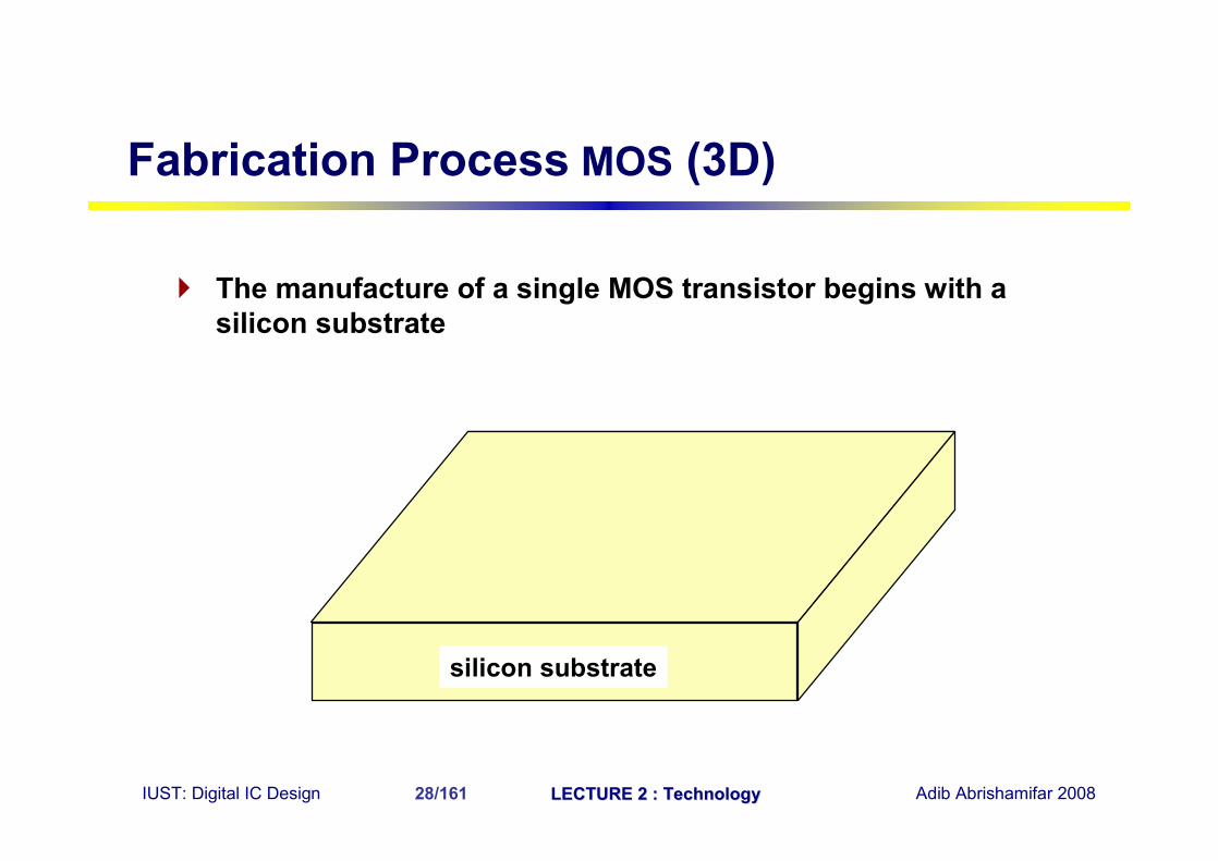
silicon substrate
Fabrication Process MOS (3D)
The manufacture of a single MOS transistor begins with a silicon substrate
IUST: Digital IC Design LECTURE 2 : TechnologyLECTURE 2 : Technology Adib Abrishamifar 200829/161
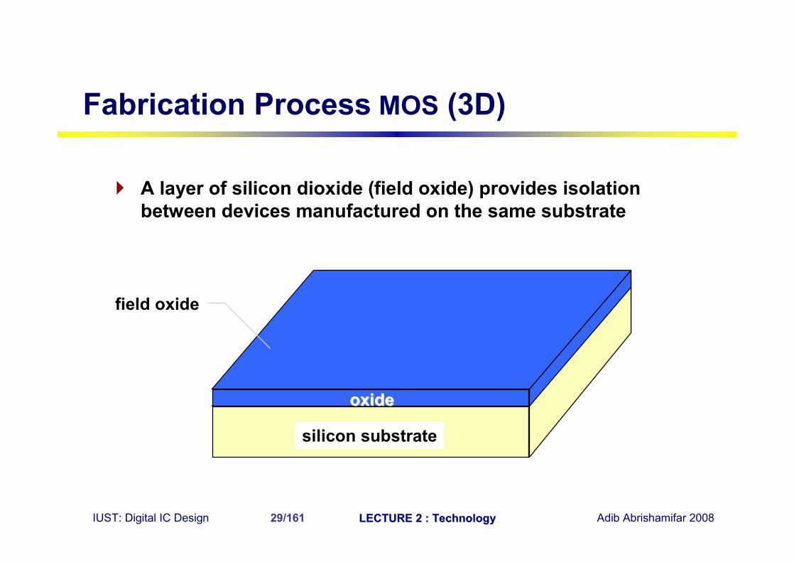
silicon substrate
oxideoxide
field oxide
A layer of silicon dioxide (field oxide) provides isolation between devices manufactured on the same substrate
Fabrication Process MOS (3D)
IUST: Digital IC Design LECTURE 2 : TechnologyLECTURE 2 : Technology Adib Abrishamifar 200830/161
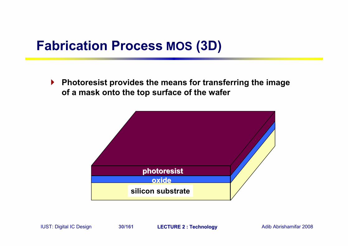
silicon substrateoxideoxide
photoresistphotoresist
Photoresist provides the means for transferring the image of a mask onto the top surface of the wafer
Fabrication Process MOS (3D)
IUST: Digital IC Design LECTURE 2 : TechnologyLECTURE 2 : Technology Adib Abrishamifar 200831/161
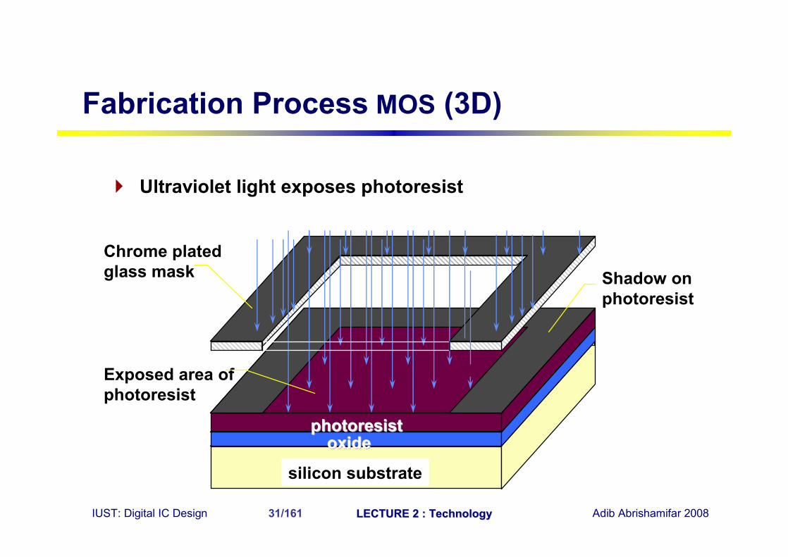
Ultraviolet Light
Shadow on photoresist
photoresistphotoresist
Exposed area of photoresist
Chrome platedglass mask
silicon substrate
oxideoxide
Ultraviolet light exposes photoresist .
Fabrication Process MOS (3D)
IUST: Digital IC Design LECTURE 2 : TechnologyLECTURE 2 : Technology Adib Abrishamifar 200832/161
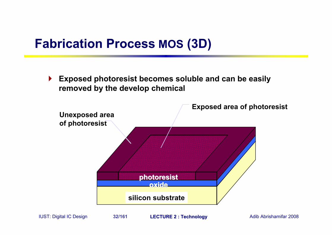
Unexposed area of photoresist
silicon substrate
Exposed area of photoresist
oxideoxidephotoresistphotoresist
Exposed photoresist becomes soluble and can be easily removed by the develop chemical
Fabrication Process MOS (3D)
IUST: Digital IC Design LECTURE 2 : TechnologyLECTURE 2 : Technology Adib Abrishamifar 200833/161
silicon substrate
oxideoxide
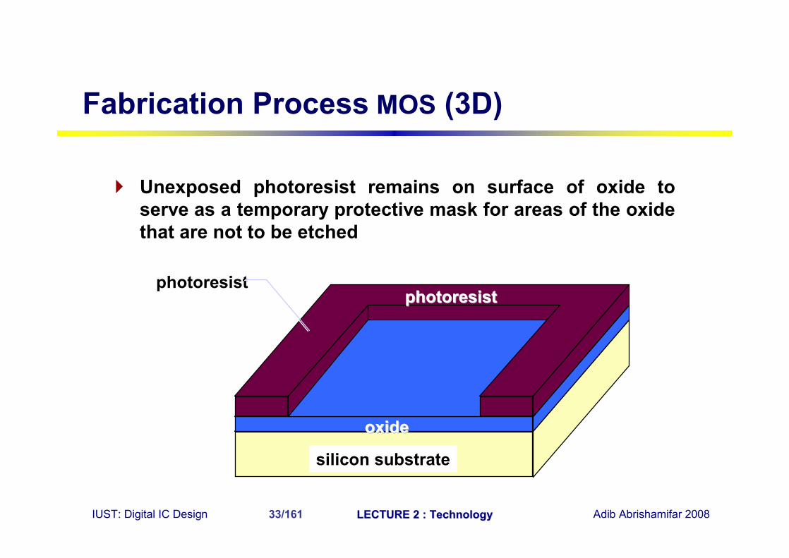
photoresistphotoresistphotoresist
Unexposed photoresist remains on surface of oxide to serve as a temporary protective mask for areas of the oxide that are not to be etched
Fabrication Process MOS (3D)
IUST: Digital IC Design LECTURE 2 : TechnologyLECTURE 2 : Technology Adib Abrishamifar 200834/161
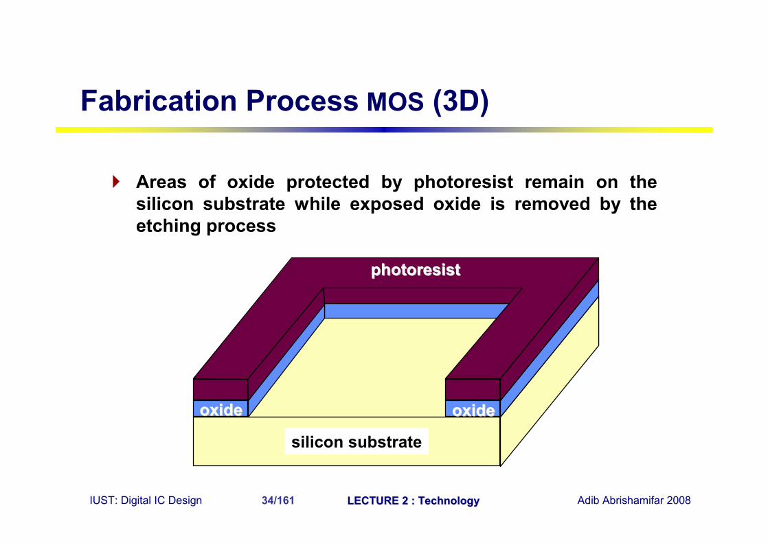
silicon substrate
oxideoxide oxideoxide
silicon substrate
photoresistphotoresist
Areas of oxide protected by photoresist remain on the silicon substrate while exposed oxide is removed by the etching process
Fabrication Process MOS (3D)
IUST: Digital IC Design LECTURE 2 : TechnologyLECTURE 2 : Technology Adib Abrishamifar 200835/161
silicon substrate
oxideoxide oxideoxide
silicon substrate
field oxide
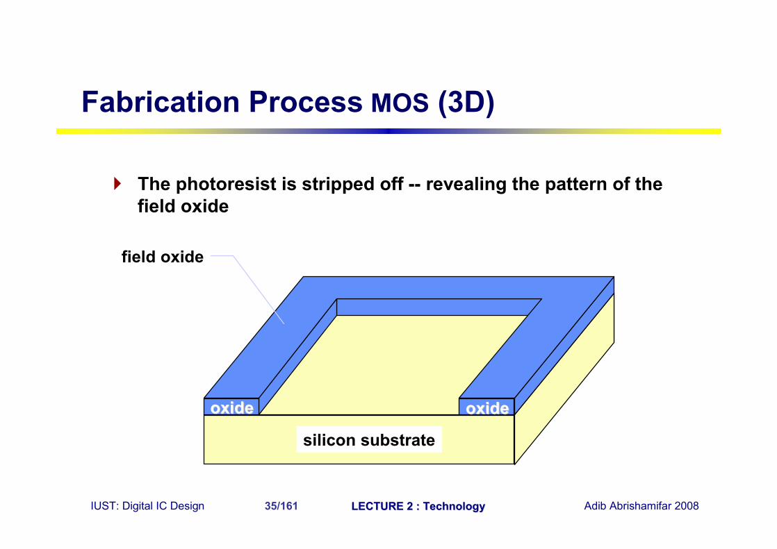
The photoresist is stripped off -- revealing the pattern of the field oxide
Fabrication Process MOS (3D)
IUST: Digital IC Design LECTURE 2 : TechnologyLECTURE 2 : Technology Adib Abrishamifar 200836/161
silicon substrate
oxideoxide oxideoxide
gate oxidegate oxide
thin oxide layer
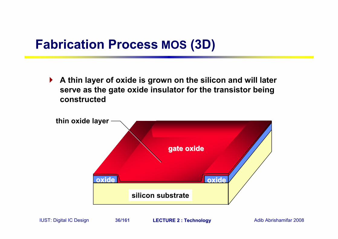
A thin layer of oxide is grown on the silicon and will later serve as the gate oxide insulator for the transistor being constructed
Fabrication Process MOS (3D)
IUST: Digital IC Design LECTURE 2 : TechnologyLECTURE 2 : Technology Adib Abrishamifar 200837/161
silicon substrate
oxideoxide oxideoxide
gate oxide
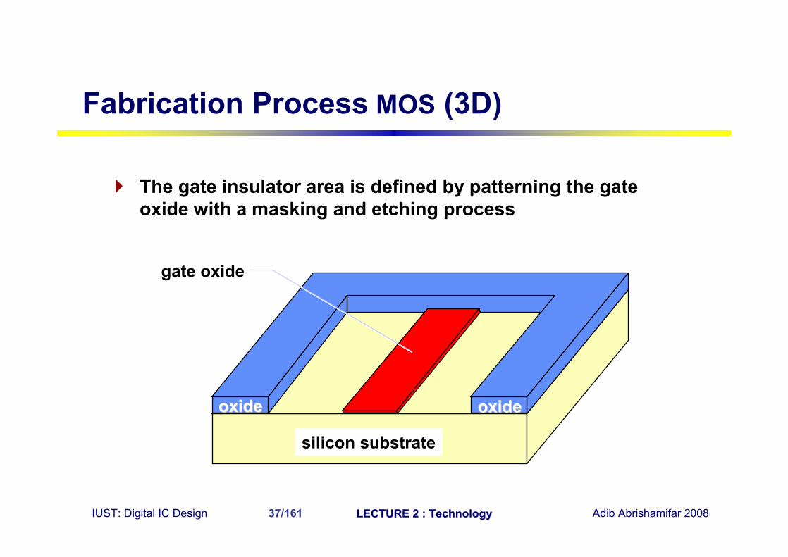
The gate insulator area is defined by patterning the gate oxide with a masking and etching process
Fabrication Process MOS (3D)
IUST: Digital IC Design LECTURE 2 : TechnologyLECTURE 2 : Technology Adib Abrishamifar 200838/161
silicon substrate
oxideoxide oxideoxide
gate oxide
polysiliconpolysilicongate oxide
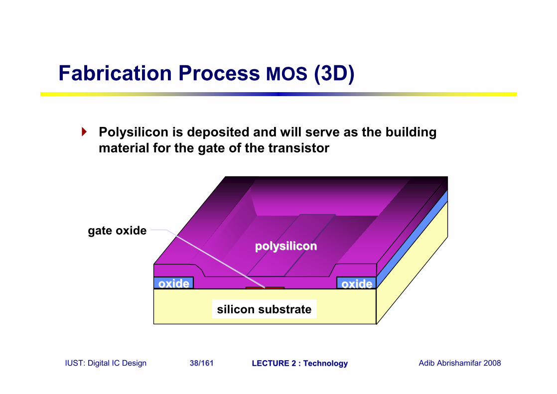
Polysilicon is deposited and will serve as the building material for the gate of the transistor
Fabrication Process MOS (3D)
IUST: Digital IC Design LECTURE 2 : TechnologyLECTURE 2 : Technology Adib Abrishamifar 200839/161
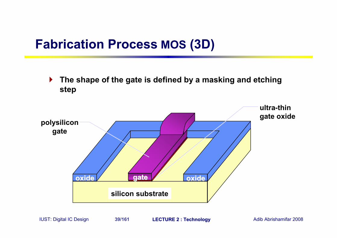
silicon substrate
oxideoxide oxideoxidegate
gategate
ultra-thin gate oxide
polysilicongate
The shape of the gate is defined by a masking and etching step
Fabrication Process MOS (3D)
IUST: Digital IC Design LECTURE 2 : TechnologyLECTURE 2 : Technology Adib Abrishamifar 200840/161
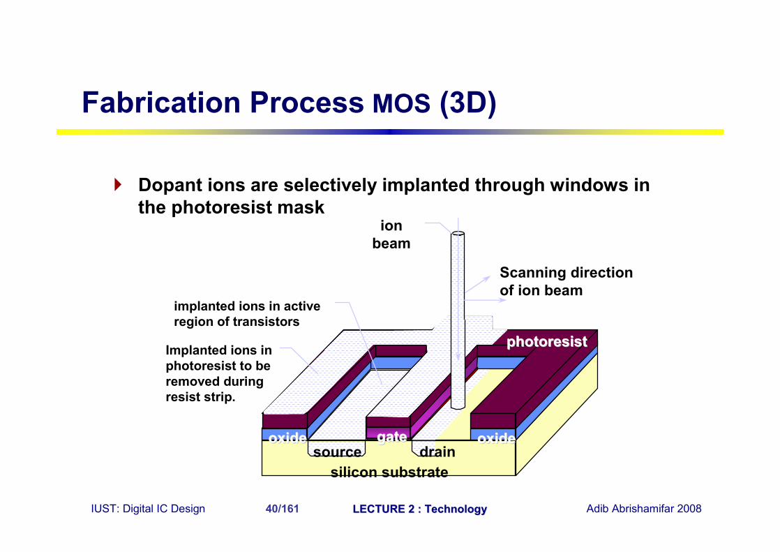
silicon substrate
oxideoxide oxideoxidegategategate
photoresistphotoresist
Scanning direction of ion beam
implanted ions in active region of transistors
Implanted ions in photoresist to be removed during resist strip.
source drain
ion beam
Dopant ions are selectively implanted through windows in the photoresist mask
Fabrication Process MOS (3D)
IUST: Digital IC Design LECTURE 2 : TechnologyLECTURE 2 : Technology Adib Abrishamifar 200841/161
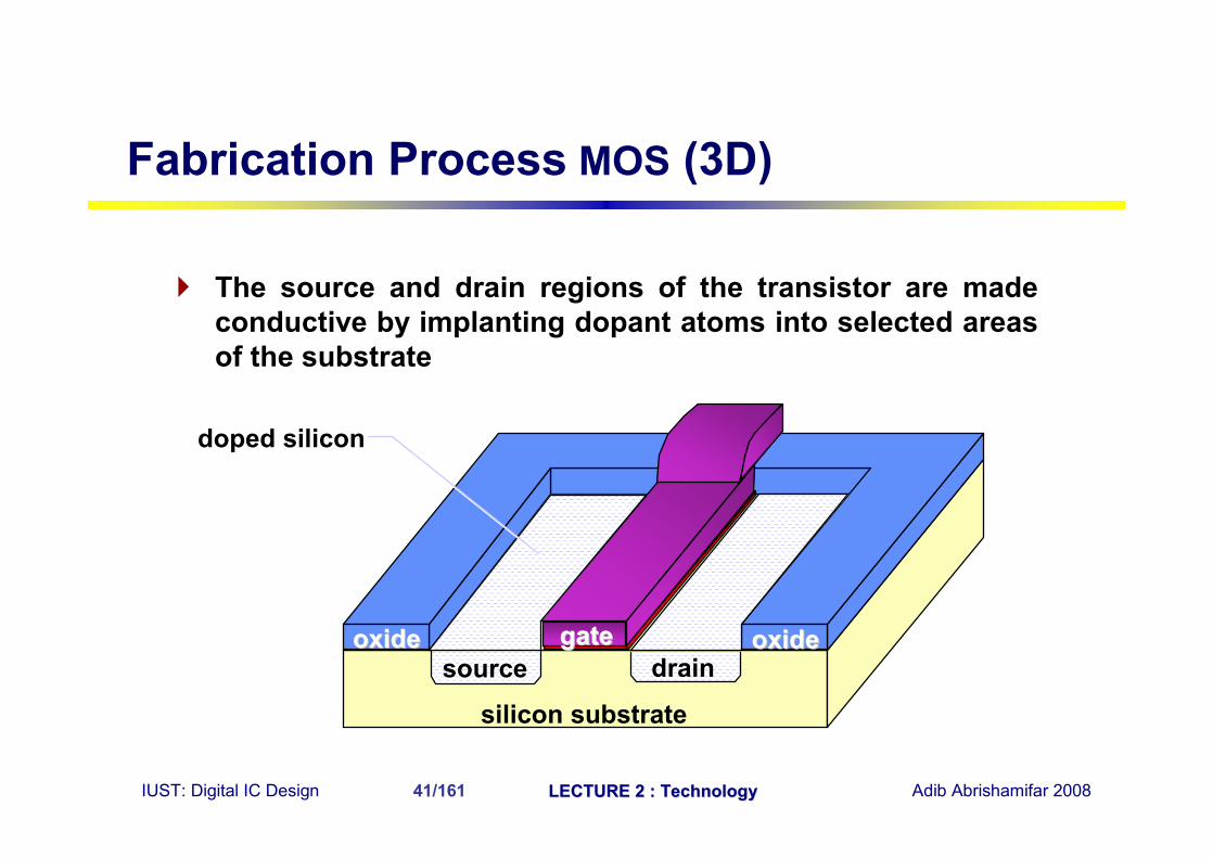
silicon substrate
oxideoxide oxideoxidegate
gategatesource drain
doped silicon
The source and drain regions of the transistor are made conductive by implanting dopant atoms into selected areas of the substrate
Fabrication Process MOS (3D)
IUST: Digital IC Design LECTURE 2 : TechnologyLECTURE 2 : Technology Adib Abrishamifar 200842/161
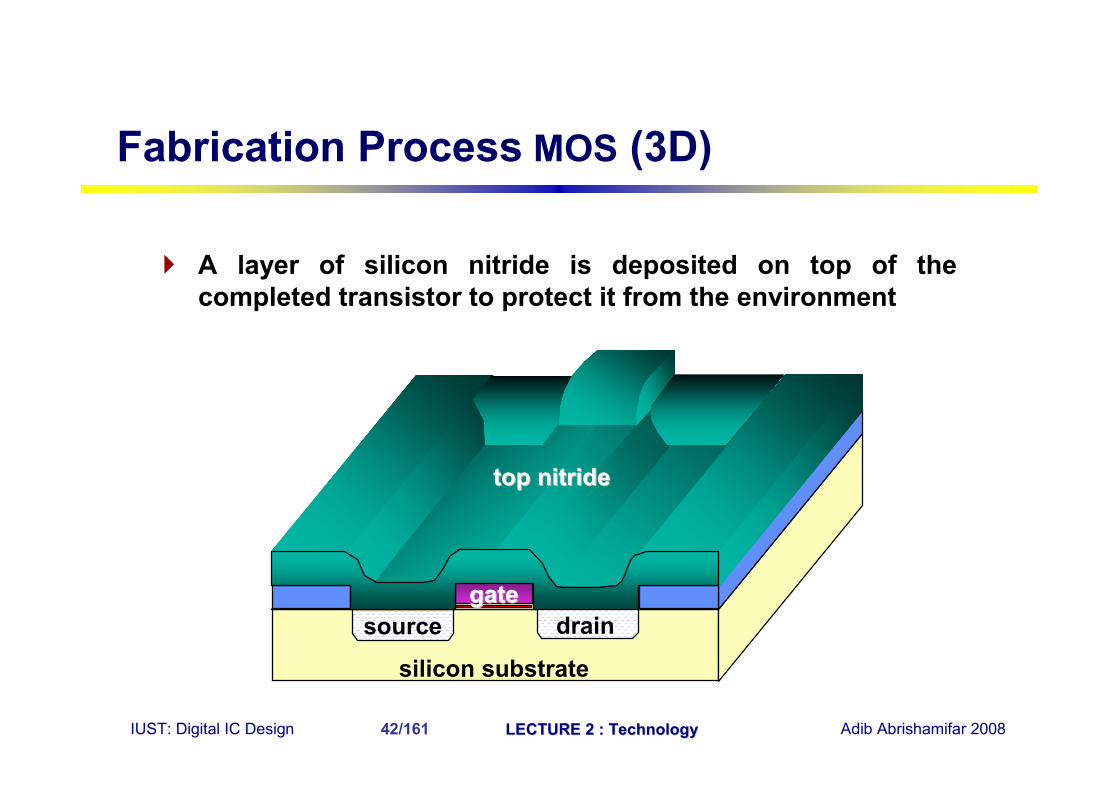
silicon substrate
source draingategate
top nitridetop nitride
A layer of silicon nitride is deposited on top of the completed transistor to protect it from the environment
Fabrication Process MOS (3D)
IUST: Digital IC Design LECTURE 2 : TechnologyLECTURE 2 : Technology Adib Abrishamifar 200843/161
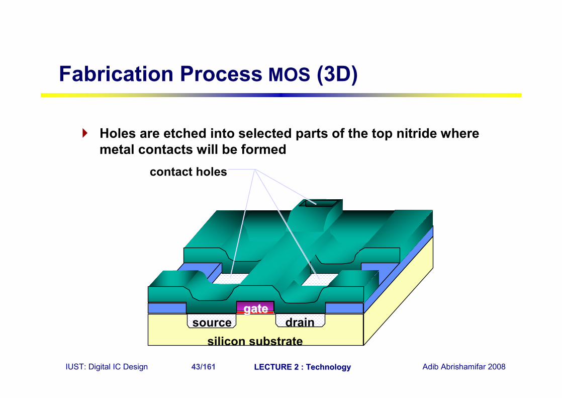
silicon substratesource drain
gategate
contact holes
Holes are etched into selected parts of the top nitride where metal contacts will be formed
Fabrication Process MOS (3D)
IUST: Digital IC Design LECTURE 2 : TechnologyLECTURE 2 : Technology Adib Abrishamifar 200844/161
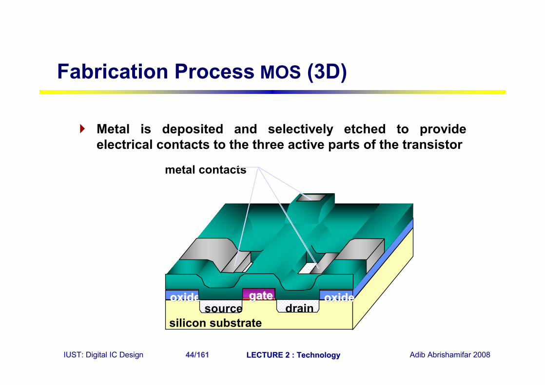
silicon substratesource drain
gategateoxideoxide oxideoxide
metal contacts
Metal is deposited and selectively etched to provide electrical contacts to the three active parts of the transistor
Fabrication Process MOS (3D)
IUST: Digital IC Design LECTURE 2 : TechnologyLECTURE 2 : Technology Adib Abrishamifar 200845/161
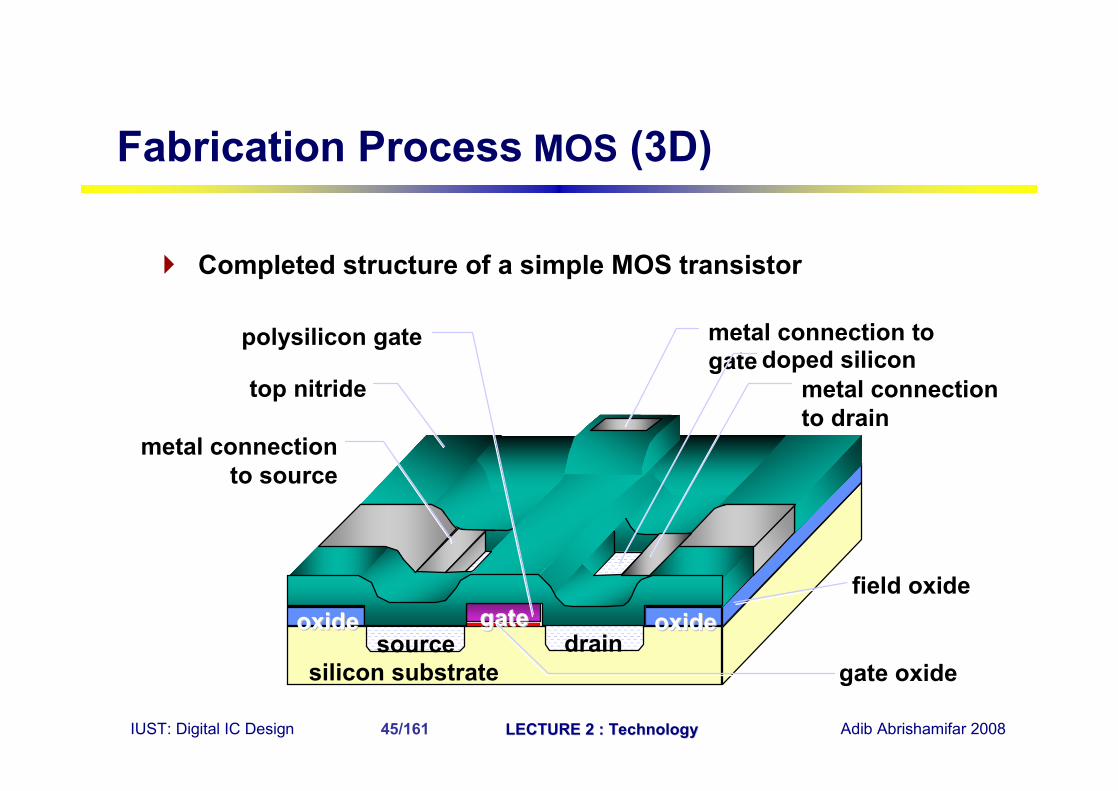
silicon substratesource drain
gategateoxideoxide oxideoxide
top nitride
metal connection to source
metal connection to gate
metal connection to drain
polysilicon gatedoped silicon
field oxide
gate oxide
Completed structure of a simple MOS transistor
Fabrication Process MOS (3D)
IUST: Digital IC Design LECTURE 2 : TechnologyLECTURE 2 : Technology Adib Abrishamifar 200846/161
Planarization Copper Interconnect Low-k dielectric for interconnect High-k dielectric for transistor gates Optical problems (and fixes)
Current Trends in Fabrication
IUST: Digital IC Design LECTURE 2 : TechnologyLECTURE 2 : Technology Adib Abrishamifar 200847/161
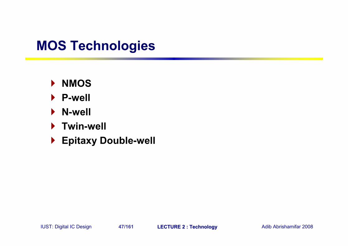
NMOS P-well N-well Twin-well Epitaxy Double-well
MOS Technologies
IUST: Digital IC Design LECTURE 2 : TechnologyLECTURE 2 : Technology Adib Abrishamifar 200848/161
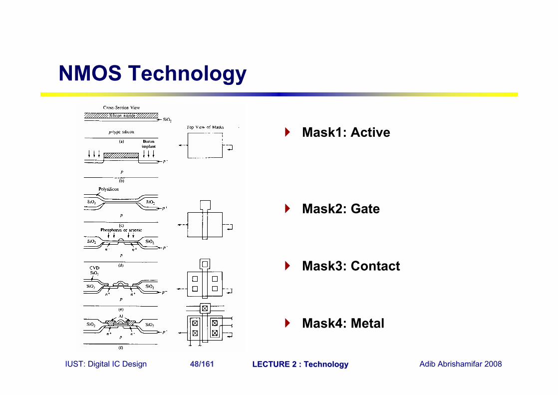
NMOS Technology
Mask1: Active
Mask2: Gate
Mask3: Contact
Mask4: Metal
IUST: Digital IC Design LECTURE 2 : TechnologyLECTURE 2 : Technology Adib Abrishamifar 200849/161
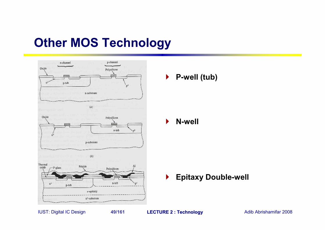
P-well (tub)
N-well
Epitaxy Double-well
Other MOS Technology
IUST: Digital IC Design LECTURE 2 : TechnologyLECTURE 2 : Technology Adib Abrishamifar 200850/161
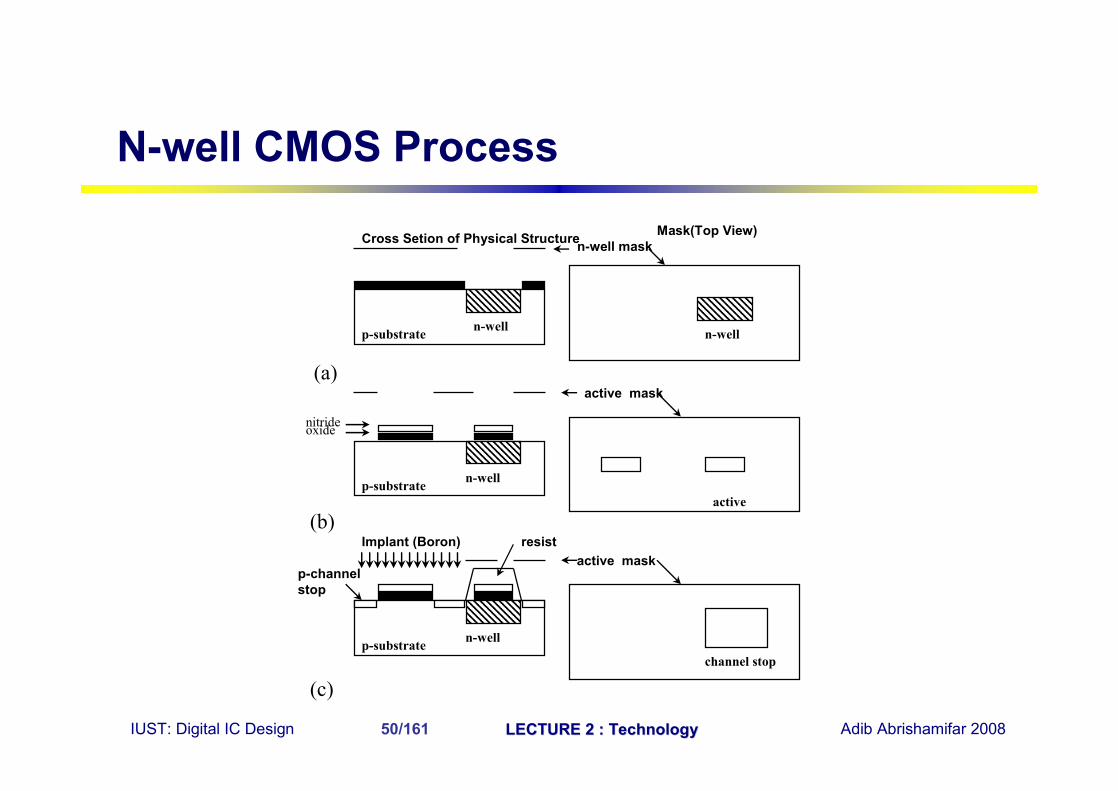
N-well CMOS Process
n-well
n-well maskMask(Top View)Cross Setion of Physical Structure
p-substrate n-well
p-substrate n-well
p-substrate n-well
active mask
active
nitrideoxide
p-channelstop
active maskresistImplant (Boron)
channel stop
(a)
(b)
(c)
IUST: Digital IC Design LECTURE 2 : TechnologyLECTURE 2 : Technology Adib Abrishamifar 200851/161
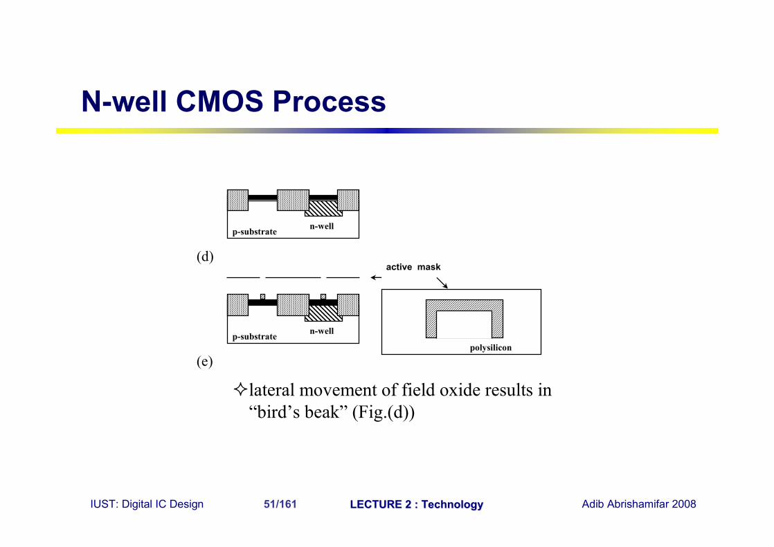
N-well CMOS Process
p-substrate n-well
active mask
p-substrate n-well
polysilicon
²lateral movement of field oxide results in “bird’s beak” (Fig.(d))
(e)
(d)
IUST: Digital IC Design LECTURE 2 : TechnologyLECTURE 2 : Technology Adib Abrishamifar 200852/161
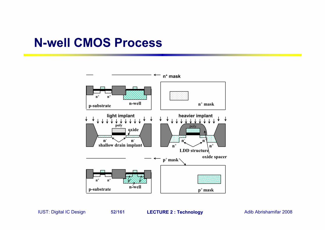
N-well CMOS Process
n+ n+
p-substrate n-wellp+ p+
n+ n+
p-substrate n-well
n+ mask
n+ mask
p+ mask
p+ mask
poly
light implant
oxide
n- n-
shallow drain implant
poly
heavier implant
n- n-
n+ n+
LDD structureoxide spacer
IUST: Digital IC Design LECTURE 2 : TechnologyLECTURE 2 : Technology Adib Abrishamifar 200853/161
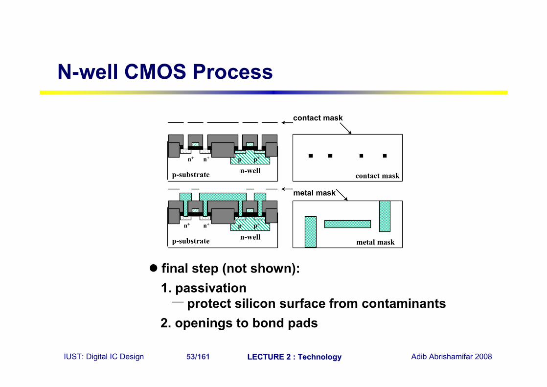
N-well CMOS Process
n+ n+
p-substrate n-wellp+ p+
n+ n+
p-substrate n-wellp+ p+
contact mask
metal mask
contact mask
metal mask
l final step (not shown):1. passivation
protect silicon surface from contaminants2. openings to bond pads
IUST: Digital IC Design LECTURE 2 : TechnologyLECTURE 2 : Technology Adib Abrishamifar 200854/161
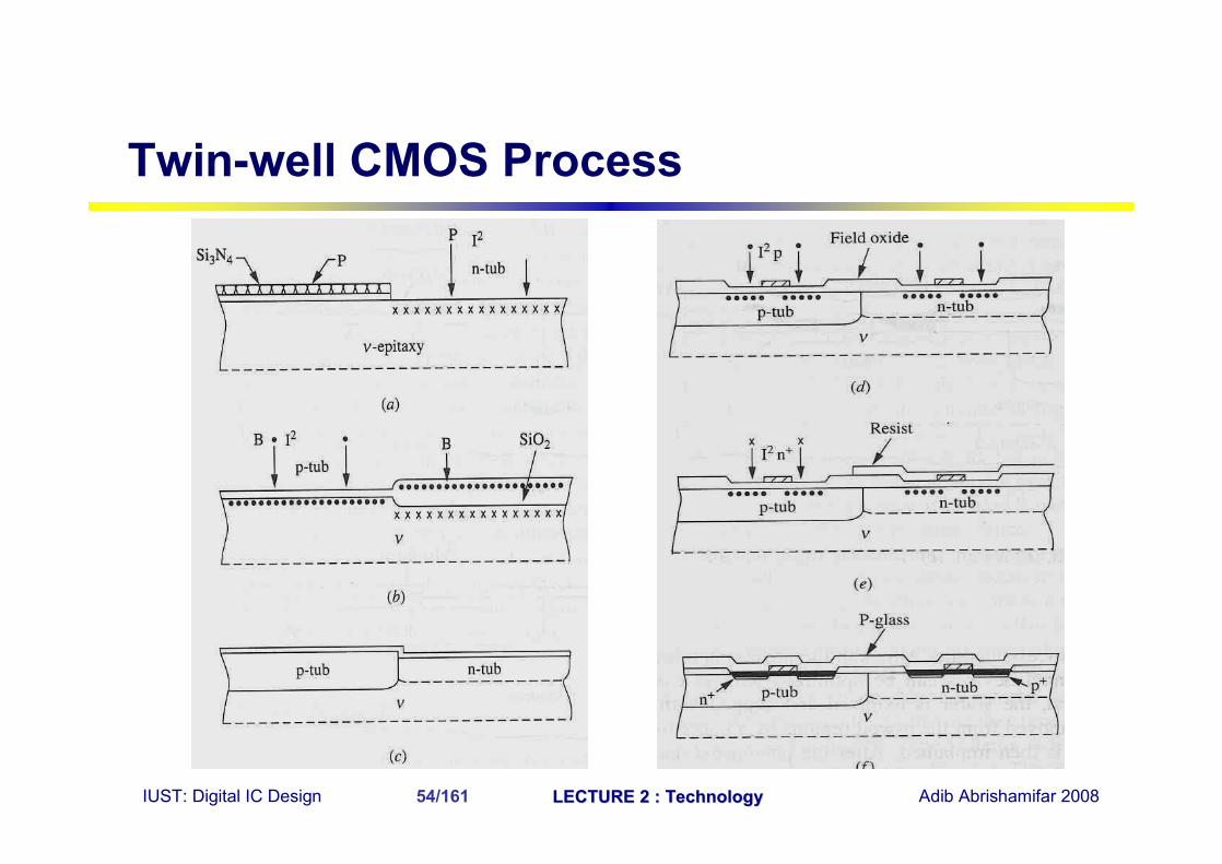
Twin-well CMOS Process
IUST: Digital IC Design LECTURE 2 : TechnologyLECTURE 2 : Technology Adib Abrishamifar 200855/161
Modern CMOS Processes
Dual-Well Trench-Isolated Shallow Trench
IUST: Digital IC Design LECTURE 2 : TechnologyLECTURE 2 : Technology Adib Abrishamifar 200856/161
p-
p-epip well n well
p+n+
gate oxide
Al (Cu)
tungsten
SiO2
SiO2
TiSi2
field oxide
Dual-Well Trench-Isolated
IUST: Digital IC Design LECTURE 2 : TechnologyLECTURE 2 : Technology Adib Abrishamifar 200857/161
p+
p-epi Base material: p+ substrate with p-epi layer
p+
After plasma etch of insulating trenches using the inverse of the active area mask
p+
p-epi SiO2
3SiN
4
After deposition of gate-oxide and sacrifical nitride (acts as a buffer layer)
Dual-Well Trench-Isolated Walk-Through
IUST: Digital IC Design LECTURE 2 : TechnologyLECTURE 2 : Technology Adib Abrishamifar 200858/161
SiO2 After trench filling, CMP planarization, and removal of sacrificial nitride
After n-well and VTpadjust implants
n
After p-well and VTnadjust implants
p
Dual-Well Trench-Isolated Walk-Through
IUST: Digital IC Design LECTURE 2 : TechnologyLECTURE 2 : Technology Adib Abrishamifar 200859/161
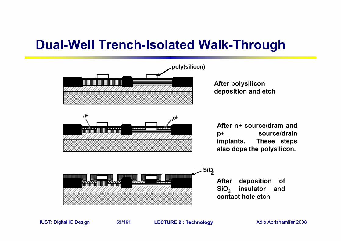
After polysilicondeposition and etch
poly(silicon)
After n+ source/dram and p+ source/drain implants. These steps also dope the polysilicon.
p+n+
After deposition of SiO2 insulator and contact hole etch
SiO2
Dual-Well Trench-Isolated Walk-Through
IUST: Digital IC Design LECTURE 2 : TechnologyLECTURE 2 : Technology Adib Abrishamifar 200860/161
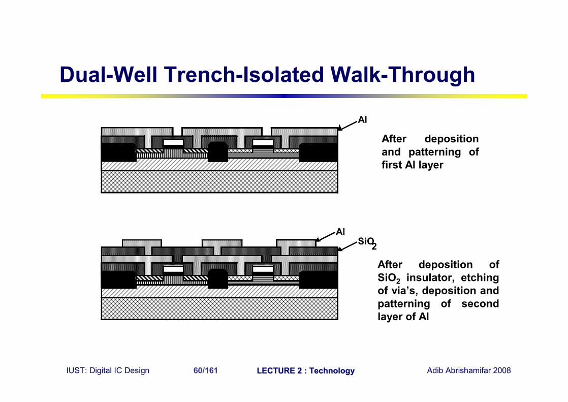
After deposition and patterning of first Al layer
Al
After deposition of SiO2 insulator, etching of via’s, deposition and patterning of second layer of Al
AlSiO2
Dual-Well Trench-Isolated Walk-Through
IUST: Digital IC Design LECTURE 2 : TechnologyLECTURE 2 : Technology Adib Abrishamifar 200861/161
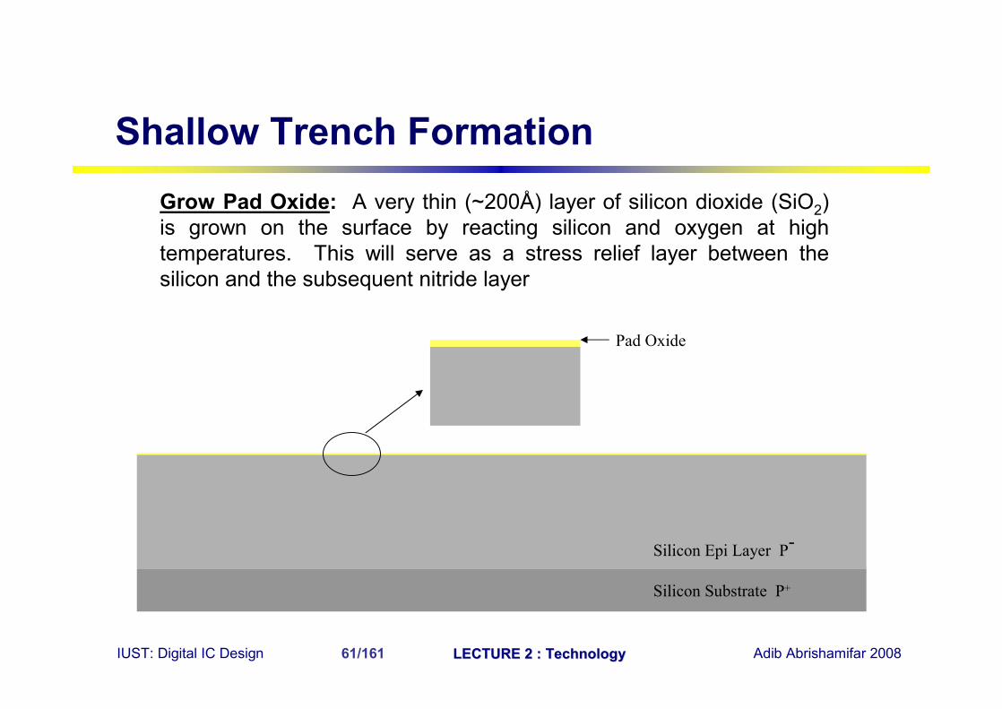
Grow Pad Oxide: A very thin (~200Å) layer of silicon dioxide (SiO2) is grown on the surface by reacting silicon and oxygen at high temperatures. This will serve as a stress relief layer between the silicon and the subsequent nitride layer
Silicon Substrate P+
Silicon Epi Layer P-
Pad Oxide
Shallow Trench Formation
IUST: Digital IC Design LECTURE 2 : TechnologyLECTURE 2 : Technology Adib Abrishamifar 200862/161
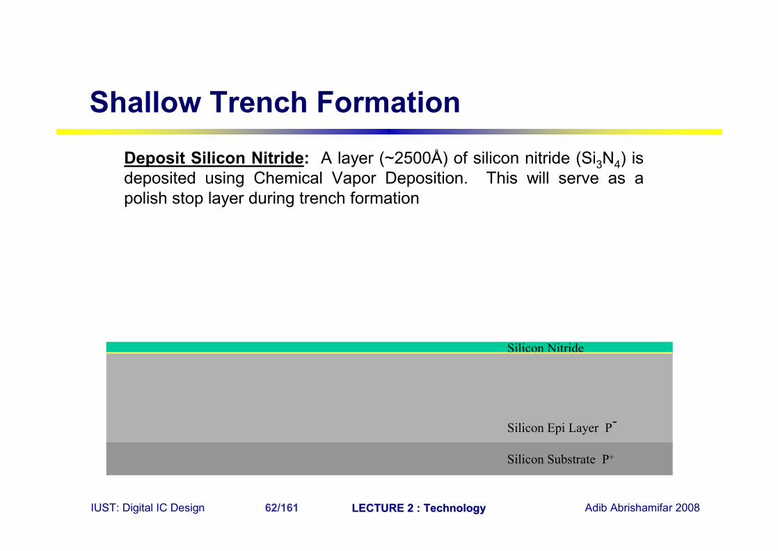
Deposit Silicon Nitride: A layer (~2500Å) of silicon nitride (Si3N4) is deposited using Chemical Vapor Deposition. This will serve as apolish stop layer during trench formation
Silicon Substrate P+
Silicon Epi Layer P-
Silicon Nitride
Shallow Trench Formation
IUST: Digital IC Design LECTURE 2 : TechnologyLECTURE 2 : Technology Adib Abrishamifar 200863/161
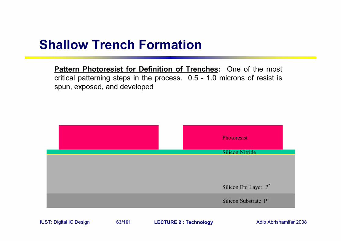
Pattern Photoresist for Definition of Trenches: One of the most critical patterning steps in the process. 0.5 - 1.0 microns of resist is spun, exposed, and developed
Silicon Substrate P+
Silicon Epi Layer P-
Silicon Nitride
Photoresist
Shallow Trench Formation
IUST: Digital IC Design LECTURE 2 : TechnologyLECTURE 2 : Technology Adib Abrishamifar 200864/161
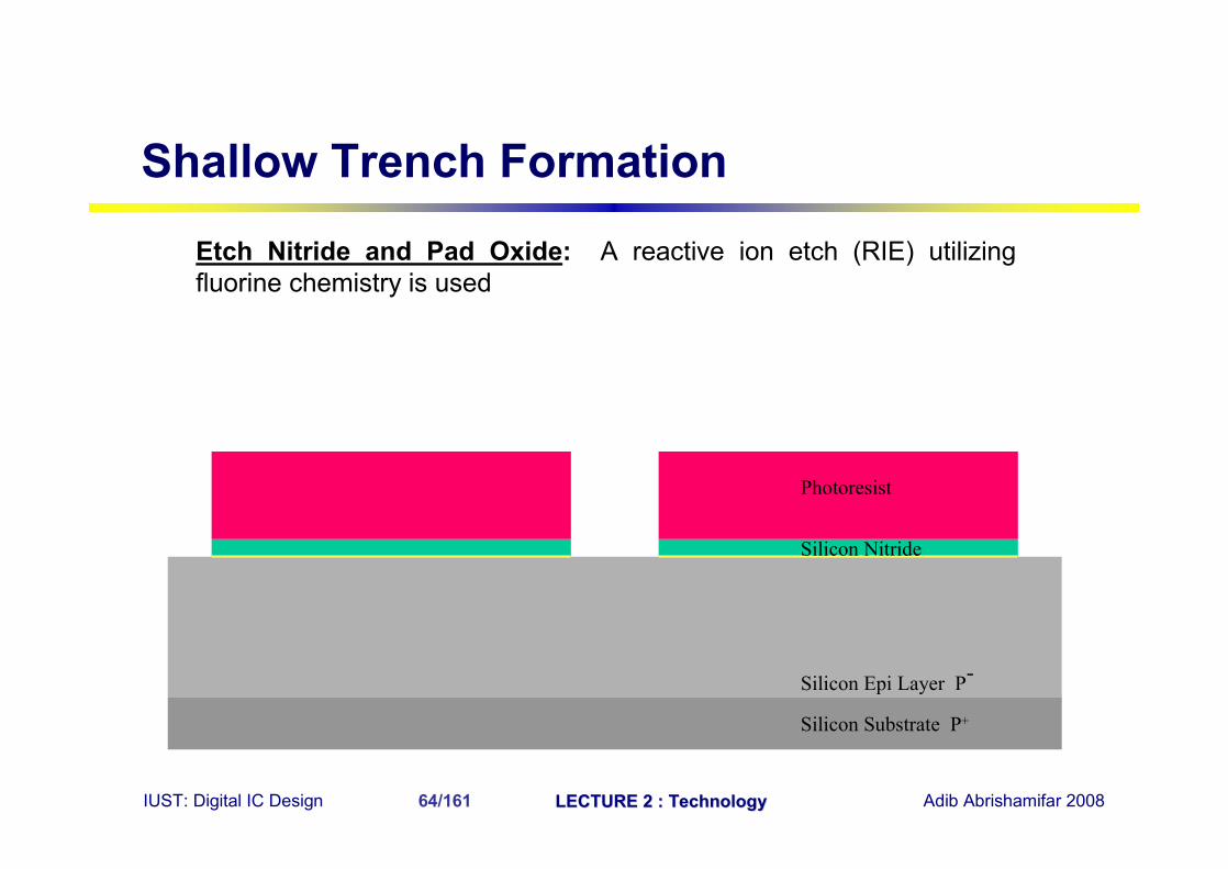
Etch Nitride and Pad Oxide: A reactive ion etch (RIE) utilizing fluorine chemistry is used
Silicon Substrate P+
Silicon Epi Layer P-
Silicon Nitride
Photoresist
Shallow Trench Formation
IUST: Digital IC Design LECTURE 2 : TechnologyLECTURE 2 : Technology Adib Abrishamifar 200865/161
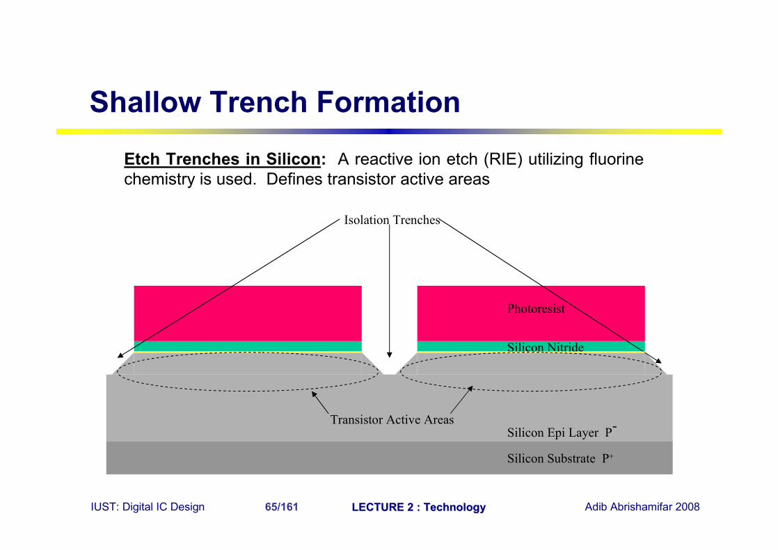
Etch Trenches in Silicon: A reactive ion etch (RIE) utilizing fluorine chemistry is used. Defines transistor active areas
Silicon Substrate P+
Silicon Epi Layer P-
Silicon Nitride
Photoresist
Transistor Active Areas
Isolation Trenches
Shallow Trench Formation
IUST: Digital IC Design LECTURE 2 : TechnologyLECTURE 2 : Technology Adib Abrishamifar 200866/161
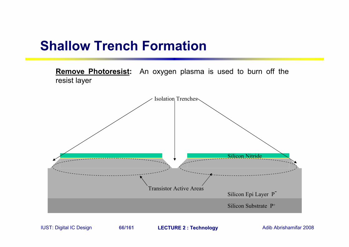
Remove Photoresist: An oxygen plasma is used to burn off the resist layer
Silicon Substrate P+
Silicon Epi Layer P-
Silicon Nitride
Transistor Active Areas
Isolation Trenches
Shallow Trench Formation
IUST: Digital IC Design LECTURE 2 : TechnologyLECTURE 2 : Technology Adib Abrishamifar 200867/161
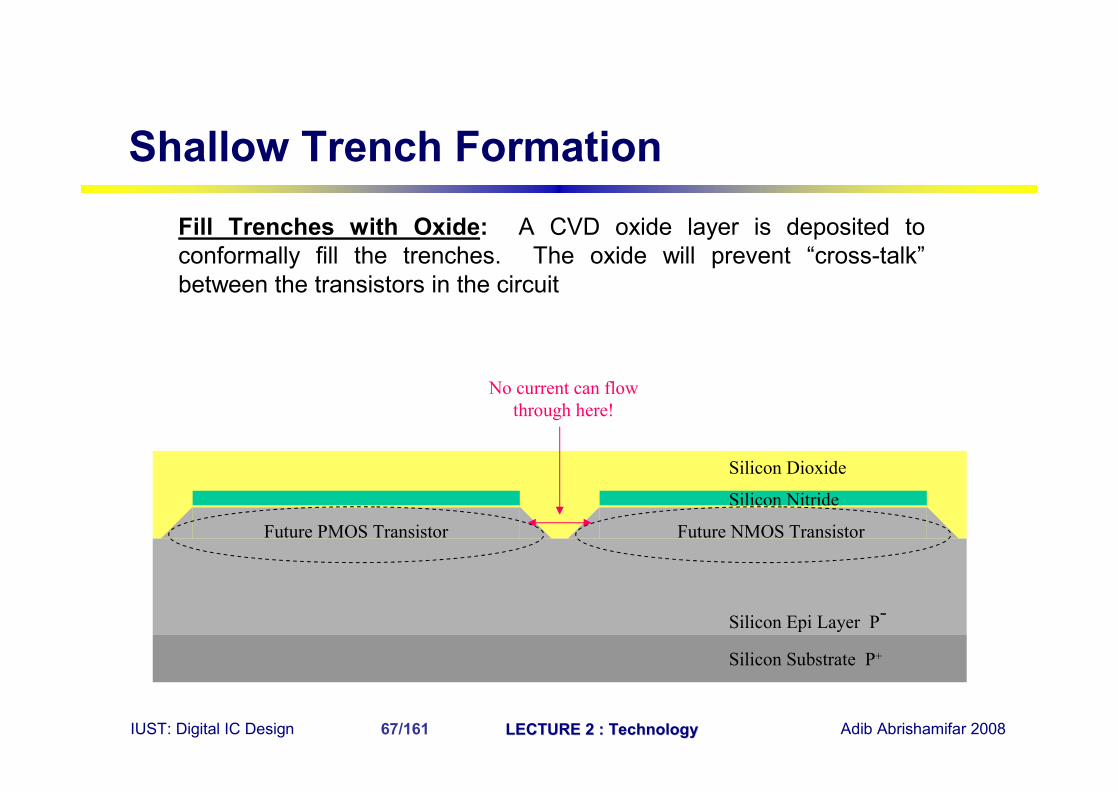
Fill Trenches with Oxide: A CVD oxide layer is deposited to conformally fill the trenches. The oxide will prevent “cross-talk”between the transistors in the circuit
Silicon Substrate P+
Silicon Epi Layer P-
Silicon Nitride
Future PMOS Transistor
Silicon Dioxide
Future NMOS Transistor
No current can flow through here!
Shallow Trench Formation
IUST: Digital IC Design LECTURE 2 : TechnologyLECTURE 2 : Technology Adib Abrishamifar 200868/161
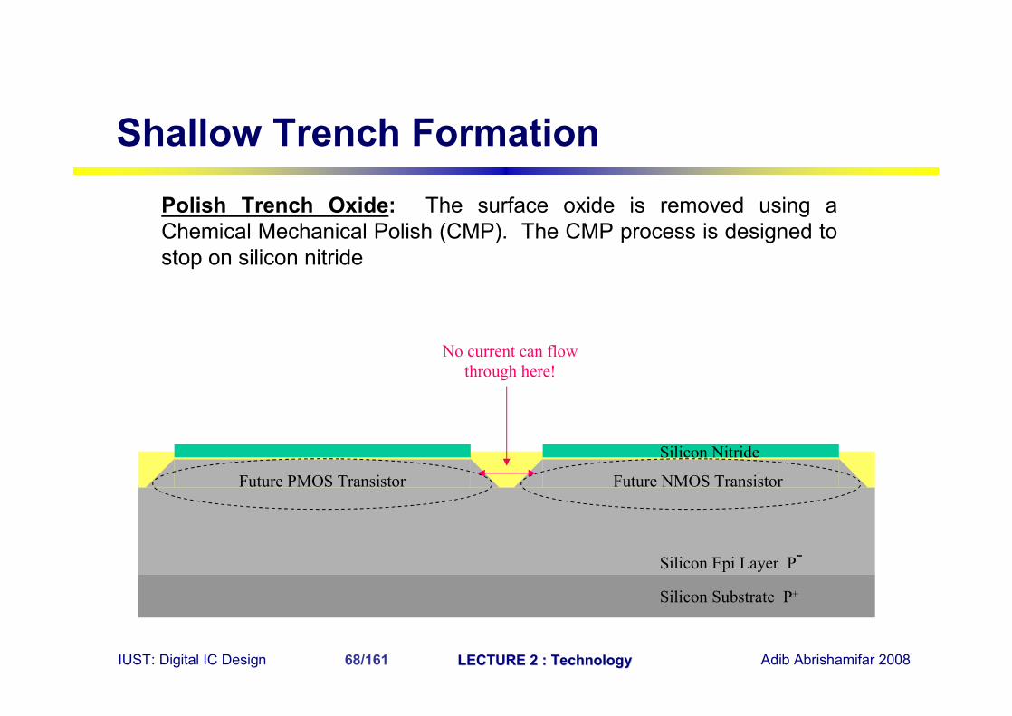
Polish Trench Oxide: The surface oxide is removed using a Chemical Mechanical Polish (CMP). The CMP process is designed to stop on silicon nitride
Silicon Substrate P+
Silicon Epi Layer P-
Silicon Nitride
Future PMOS Transistor Future NMOS Transistor
No current can flow through here!
Shallow Trench Formation
IUST: Digital IC Design LECTURE 2 : TechnologyLECTURE 2 : Technology Adib Abrishamifar 200869/161
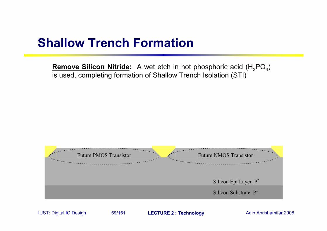
Remove Silicon Nitride: A wet etch in hot phosphoric acid (H3PO4) is used, completing formation of Shallow Trench Isolation (STI)
Silicon Substrate P+
Silicon Epi Layer P-
Future PMOS Transistor Future NMOS Transistor
Shallow Trench Formation
IUST: Digital IC Design LECTURE 2 : TechnologyLECTURE 2 : Technology Adib Abrishamifar 200870/161
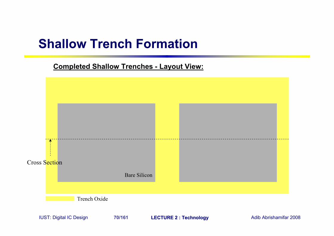
Completed Shallow Trenches - Layout View:
Trench Oxide
Cross Section
Bare Silicon
Shallow Trench Formation

IUST: Digital IC Design LECTURE 2 : TechnologyLECTURE 2 : Technology Adib Abrishamifar 200871/161
Pattern Photoresist for N-Well Formation: A non-critical masking layer, utilizing thicker resist to block the implant
Silicon Substrate P+
Silicon Epi Layer P-
Future PMOS Transistor Future NMOS Transistor
Photoresist
Shallow Trench: Well Formation
IUST: Digital IC Design LECTURE 2 : TechnologyLECTURE 2 : Technology Adib Abrishamifar 200872/161
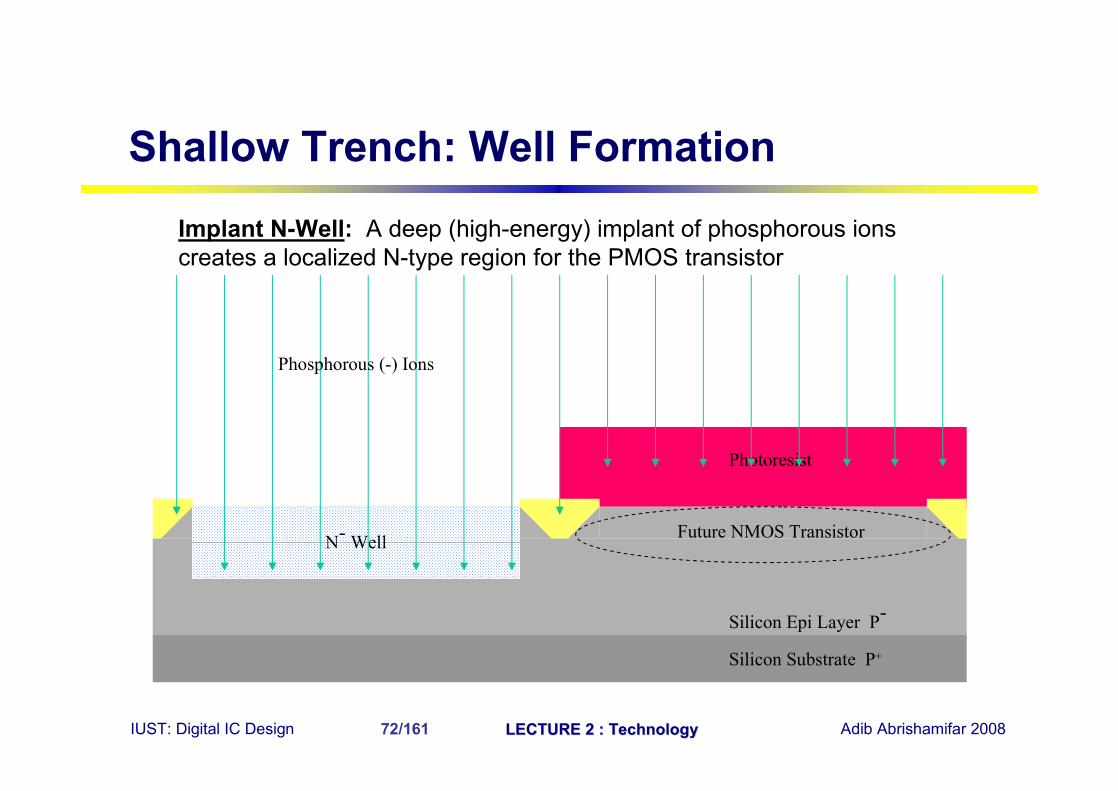
Implant N-Well: A deep (high-energy) implant of phosphorous ions creates a localized N-type region for the PMOS transistor
Silicon Substrate P+
Silicon Epi Layer P-
Future NMOS Transistor
Photoresist
N- Well
Phosphorous (-) Ions
Shallow Trench: Well Formation
IUST: Digital IC Design LECTURE 2 : TechnologyLECTURE 2 : Technology Adib Abrishamifar 200873/161
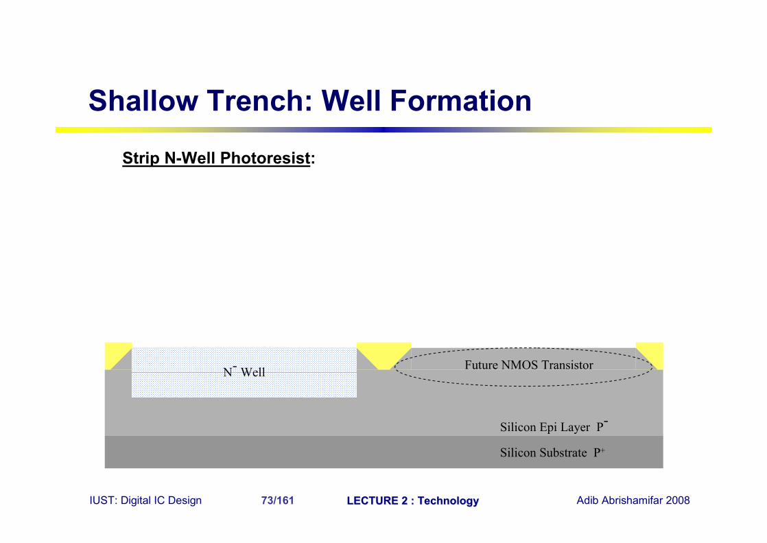
Strip N-Well Photoresist:
Silicon Substrate P+
Silicon Epi Layer P-
Future NMOS TransistorN- Well
Shallow Trench: Well Formation
IUST: Digital IC Design LECTURE 2 : TechnologyLECTURE 2 : Technology Adib Abrishamifar 200874/161
Photoresist
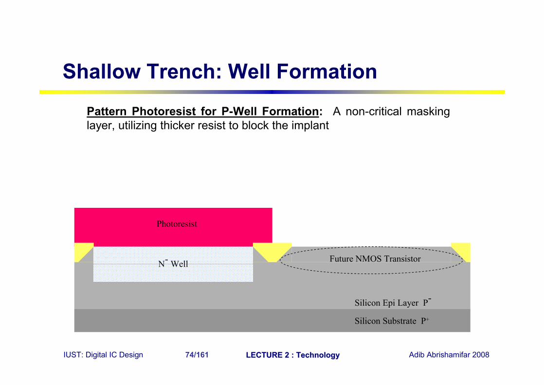
Pattern Photoresist for P-Well Formation: A non-critical masking layer, utilizing thicker resist to block the implant
Silicon Substrate P+
Silicon Epi Layer P-
Future NMOS TransistorN- Well
Shallow Trench: Well Formation
IUST: Digital IC Design LECTURE 2 : TechnologyLECTURE 2 : Technology Adib Abrishamifar 200875/161
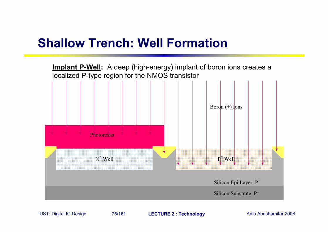
Implant P-Well: A deep (high-energy) implant of boron ions creates a localized P-type region for the NMOS transistor
Silicon Substrate P+
Silicon Epi Layer P-
Photoresist
N- Well
Boron (+) Ions
P- Well
Shallow Trench: Well Formation
IUST: Digital IC Design LECTURE 2 : TechnologyLECTURE 2 : Technology Adib Abrishamifar 200876/161
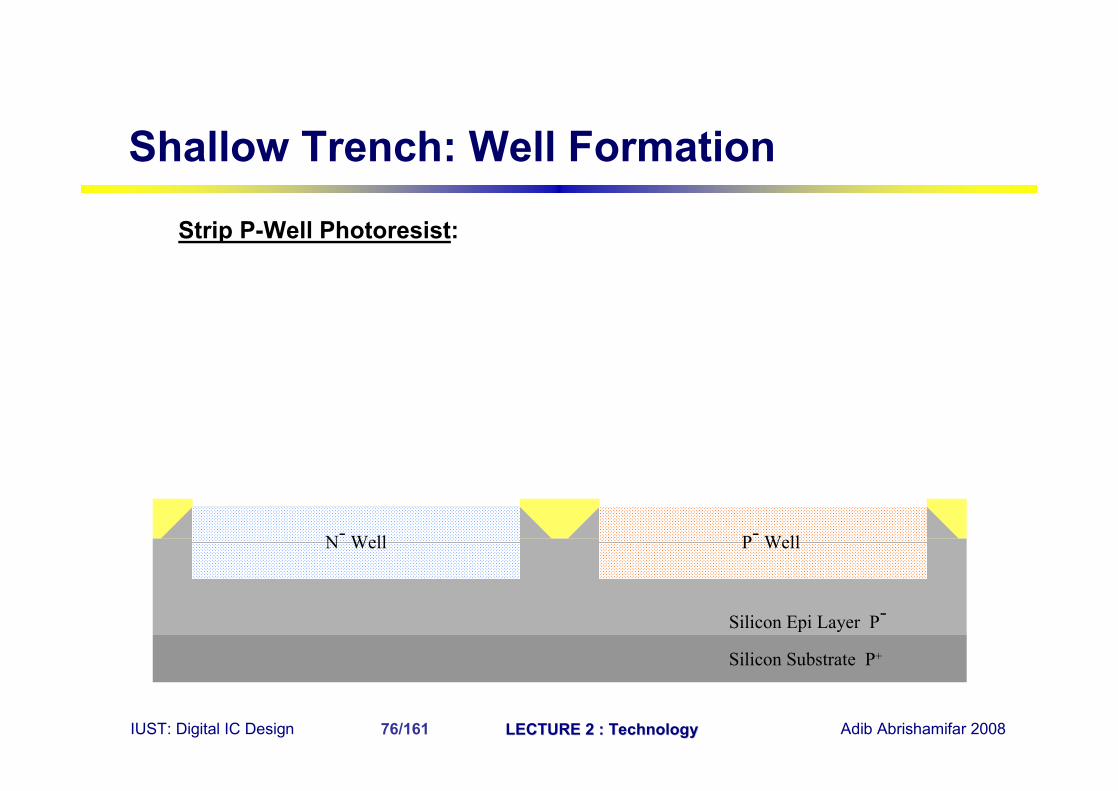
Strip P-Well Photoresist:
Silicon Substrate P+
Silicon Epi Layer P-
N- Well P- Well
Shallow Trench: Well Formation
IUST: Digital IC Design LECTURE 2 : TechnologyLECTURE 2 : Technology Adib Abrishamifar 200877/161
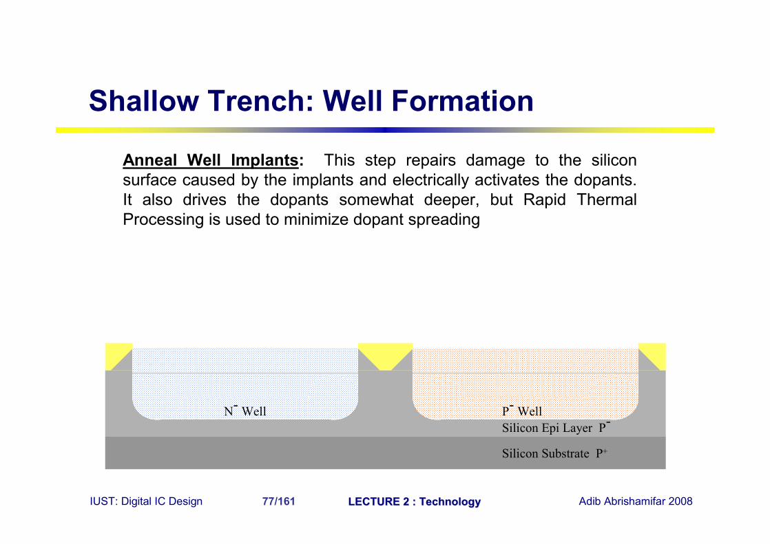
Anneal Well Implants: This step repairs damage to the silicon surface caused by the implants and electrically activates the dopants. It also drives the dopants somewhat deeper, but Rapid Thermal Processing is used to minimize dopant spreading
Silicon Substrate P+
Silicon Epi Layer P-P- WellN- Well
Shallow Trench: Well Formation
IUST: Digital IC Design LECTURE 2 : TechnologyLECTURE 2 : Technology Adib Abrishamifar 200878/161
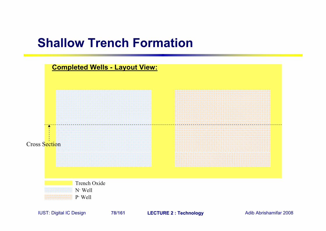
Completed Wells - Layout View:
Trench OxideN- WellP- Well
Cross Section
Shallow Trench Formation
IUST: Digital IC Design LECTURE 2 : TechnologyLECTURE 2 : Technology Adib Abrishamifar 200879/161
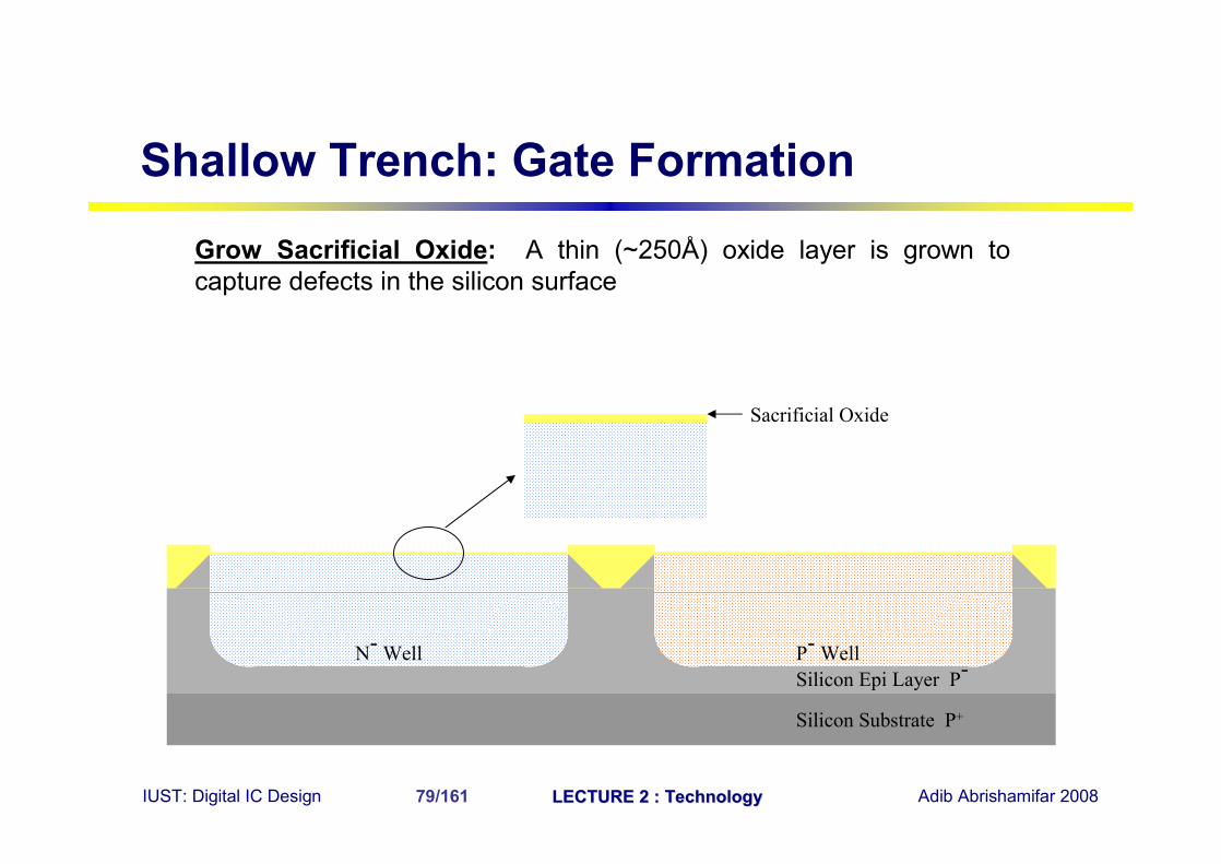
Grow Sacrificial Oxide: A thin (~250Å) oxide layer is grown to capture defects in the silicon surface
Silicon Substrate P+
Silicon Epi Layer P-P- WellN- Well
Sacrificial Oxide
Shallow Trench: Gate Formation
IUST: Digital IC Design LECTURE 2 : TechnologyLECTURE 2 : Technology Adib Abrishamifar 200880/161
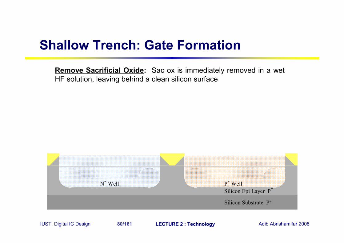
Remove Sacrificial Oxide: Sac ox is immediately removed in a wet HF solution, leaving behind a clean silicon surface
Silicon Substrate P+
Silicon Epi Layer P-P- WellN- Well
Shallow Trench: Gate Formation
IUST: Digital IC Design LECTURE 2 : TechnologyLECTURE 2 : Technology Adib Abrishamifar 200881/161
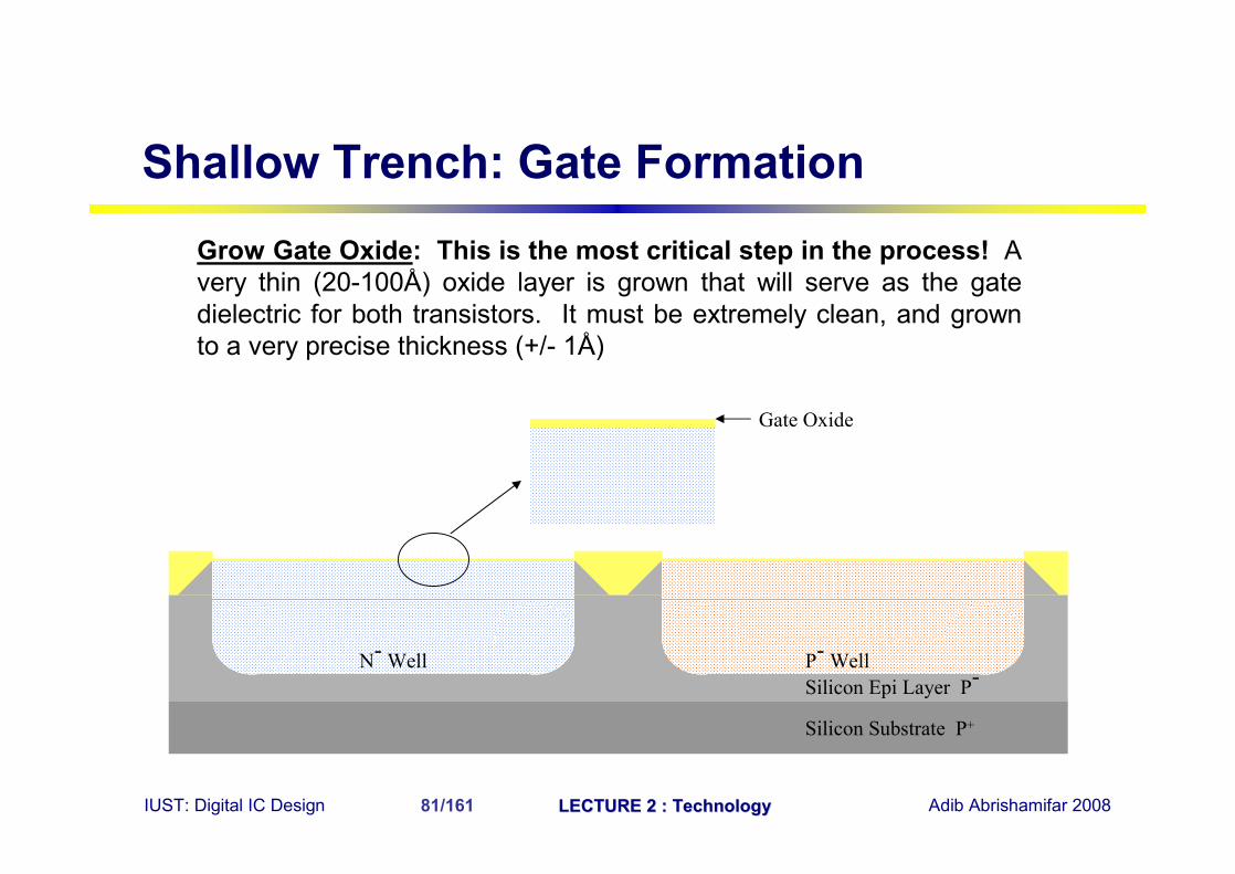
Grow Gate Oxide: This is the most critical step in the process! A very thin (20-100Å) oxide layer is grown that will serve as the gate dielectric for both transistors. It must be extremely clean, and grown to a very precise thickness (+/- 1Å)
Silicon Substrate P+
Silicon Epi Layer P-P- WellN- Well
Gate Oxide
Shallow Trench: Gate Formation
IUST: Digital IC Design LECTURE 2 : TechnologyLECTURE 2 : Technology Adib Abrishamifar 200882/161
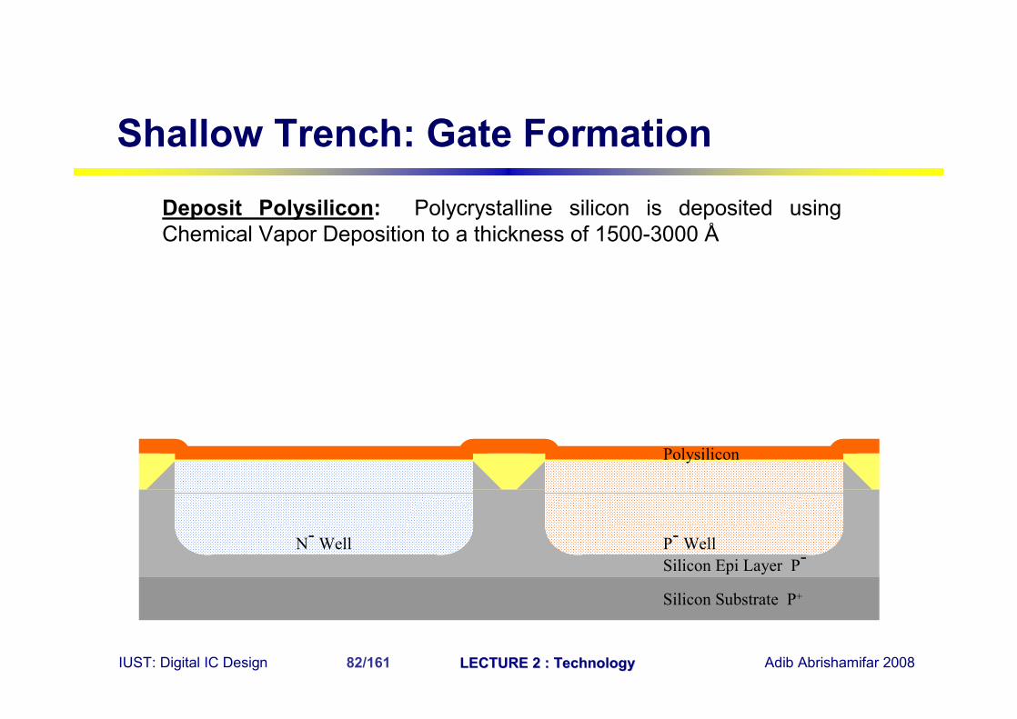
Deposit Polysilicon: Polycrystalline silicon is deposited using Chemical Vapor Deposition to a thickness of 1500-3000 Å
Silicon Substrate P+
Silicon Epi Layer P-P- WellN- Well
Polysilicon
Shallow Trench: Gate Formation
IUST: Digital IC Design LECTURE 2 : TechnologyLECTURE 2 : Technology Adib Abrishamifar 200883/161
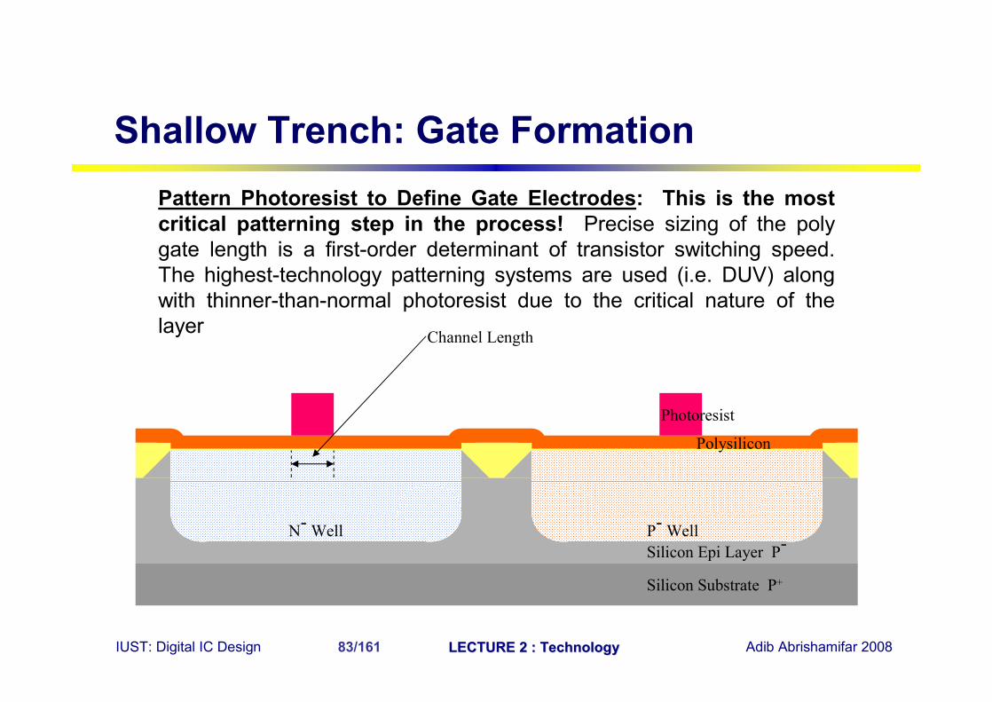
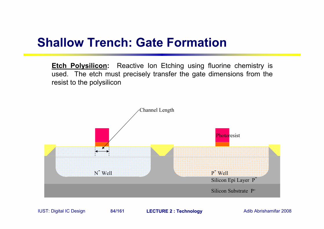
Pattern Photoresist to Define Gate Electrodes: This is the most critical patterning step in the process! Precise sizing of the poly gate length is a first-order determinant of transistor switching speed. The highest-technology patterning systems are used (i.e. DUV) along with thinner-than-normal photoresist due to the critical nature of the layer
Silicon Substrate P+
Silicon Epi Layer P-P- WellN- Well
Photoresist
Channel Length
Polysilicon
Shallow Trench: Gate Formation
IUST: Digital IC Design LECTURE 2 : TechnologyLECTURE 2 : Technology Adib Abrishamifar 200884/161
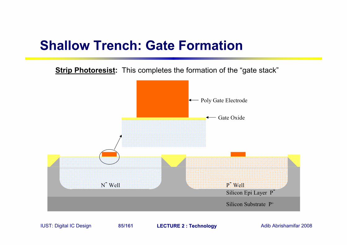
Etch Polysilicon: Reactive Ion Etching using fluorine chemistry is used. The etch must precisely transfer the gate dimensions from the resist to the polysilicon
Silicon Substrate P+
Silicon Epi Layer P-P- WellN- Well
Photoresist
Channel Length
Shallow Trench: Gate Formation
IUST: Digital IC Design LECTURE 2 : TechnologyLECTURE 2 : Technology Adib Abrishamifar 200885/161
Strip Photoresist: This completes the formation of the “gate stack”
Silicon Substrate P+
Silicon Epi Layer P-P- WellN- Well
Gate Oxide
Poly Gate Electrode
Shallow Trench: Gate Formation
IUST: Digital IC Design LECTURE 2 : TechnologyLECTURE 2 : Technology Adib Abrishamifar 200886/161
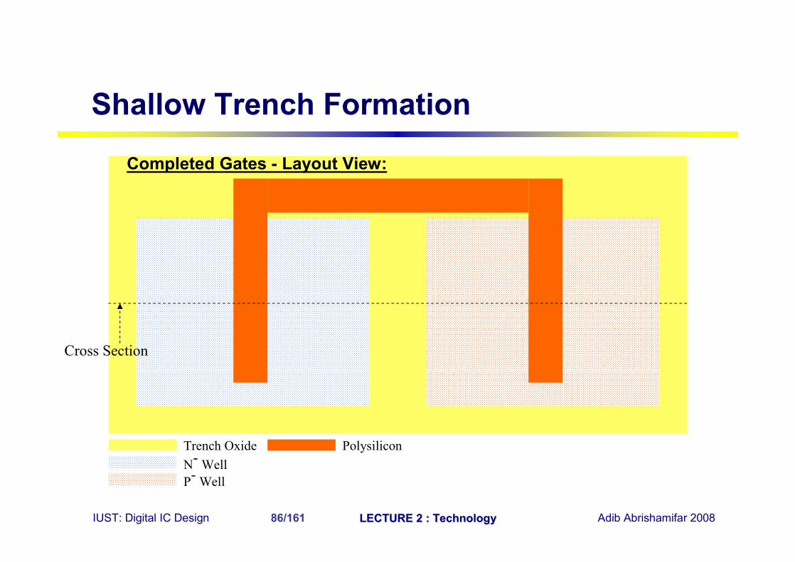
Completed Gates - Layout View:
Trench OxideN- WellP- Well
Cross Section
Polysilicon
Shallow Trench Formation
IUST: Digital IC Design LECTURE 2 : TechnologyLECTURE 2 : Technology Adib Abrishamifar 200887/161
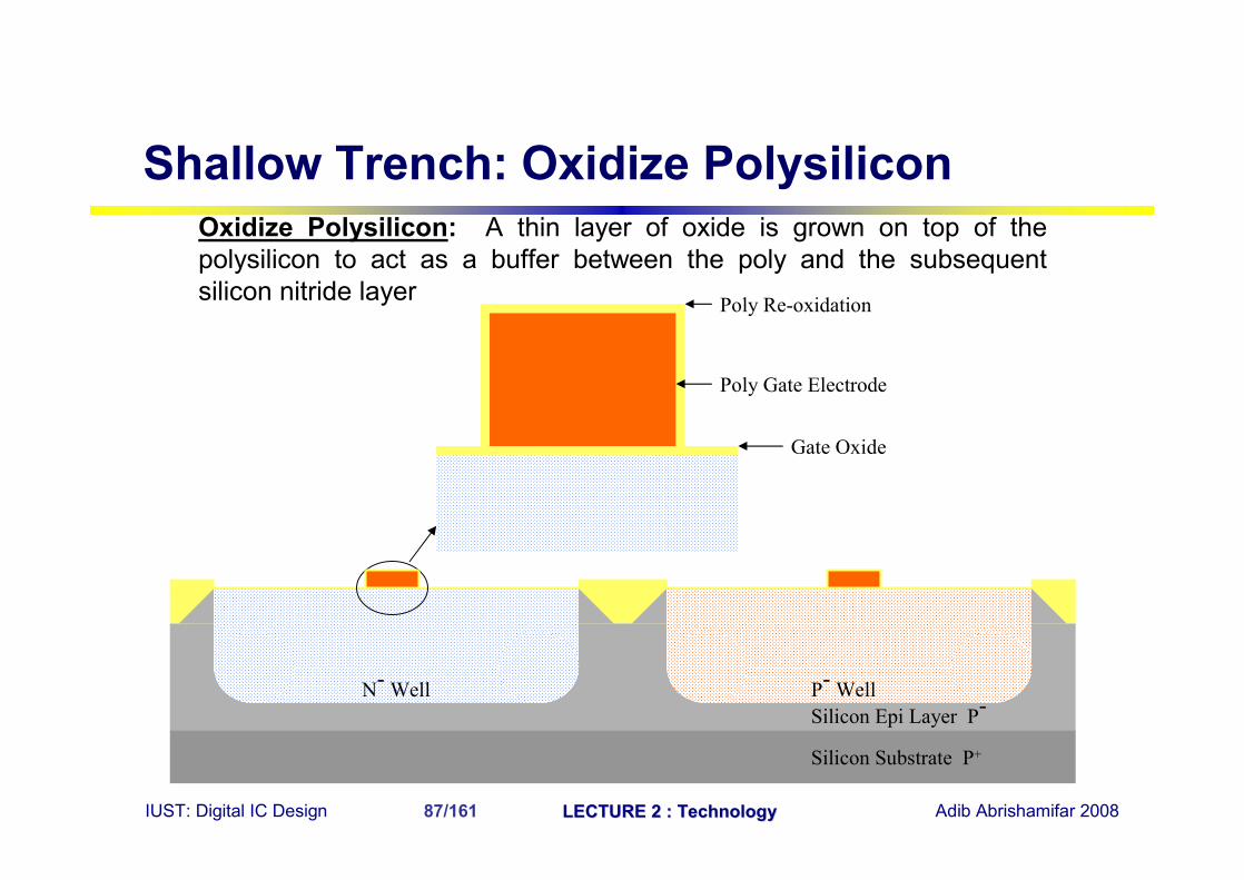
Oxidize Polysilicon: A thin layer of oxide is grown on top of the polysilicon to act as a buffer between the poly and the subsequent silicon nitride layer
Silicon Substrate P+
Silicon Epi Layer P-P- WellN- Well
Gate Oxide
Poly Gate Electrode
Poly Re-oxidation
Shallow Trench: Oxidize Polysilicon
IUST: Digital IC Design LECTURE 2 : TechnologyLECTURE 2 : Technology Adib Abrishamifar 200888/161
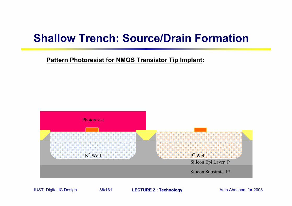
Pattern Photoresist for NMOS Transistor Tip Implant:
Silicon Substrate P+
Silicon Epi Layer P-P- WellN- Well
Photoresist
Shallow Trench: Source/Drain Formation
IUST: Digital IC Design LECTURE 2 : TechnologyLECTURE 2 : Technology Adib Abrishamifar 200889/161
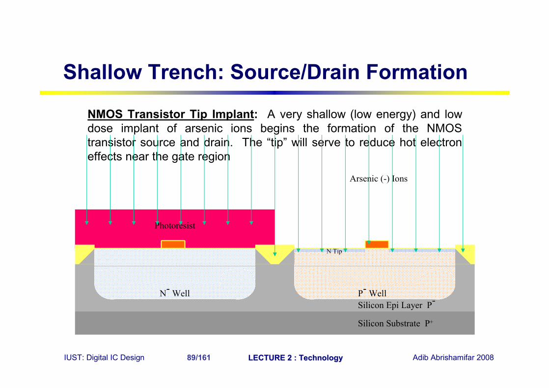
NMOS Transistor Tip Implant: A very shallow (low energy) and low dose implant of arsenic ions begins the formation of the NMOS transistor source and drain. The “tip” will serve to reduce hot electron effects near the gate region
Silicon Substrate P+
Silicon Epi Layer P-P- WellN- Well
Photoresist
Arsenic (-) Ions
N Tip
Shallow Trench: Source/Drain Formation
IUST: Digital IC Design LECTURE 2 : TechnologyLECTURE 2 : Technology Adib Abrishamifar 200890/161
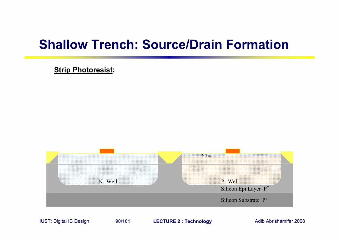
Strip Photoresist:
Silicon Substrate P+
Silicon Epi Layer P-P- WellN- Well
N Tip
Shallow Trench: Source/Drain Formation
IUST: Digital IC Design LECTURE 2 : TechnologyLECTURE 2 : Technology Adib Abrishamifar 200891/161
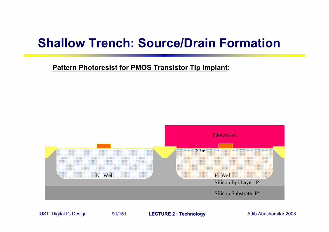
Pattern Photoresist for PMOS Transistor Tip Implant:
Silicon Substrate P+
Silicon Epi Layer P-P- WellN- Well
Photoresist
N Tip
Shallow Trench: Source/Drain Formation
IUST: Digital IC Design LECTURE 2 : TechnologyLECTURE 2 : Technology Adib Abrishamifar 200892/161
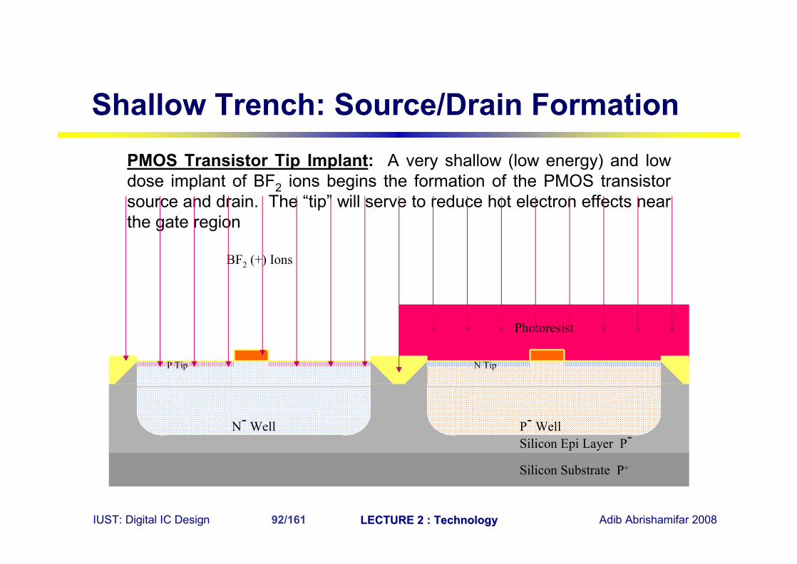
PMOS Transistor Tip Implant: A very shallow (low energy) and low dose implant of BF2 ions begins the formation of the PMOS transistor source and drain. The “tip” will serve to reduce hot electron effects near the gate region
Silicon Substrate P+
Silicon Epi Layer P-P- WellN- Well
Photoresist
BF2 (+) Ions
N TipP Tip
Shallow Trench: Source/Drain Formation
IUST: Digital IC Design LECTURE 2 : TechnologyLECTURE 2 : Technology Adib Abrishamifar 200893/161
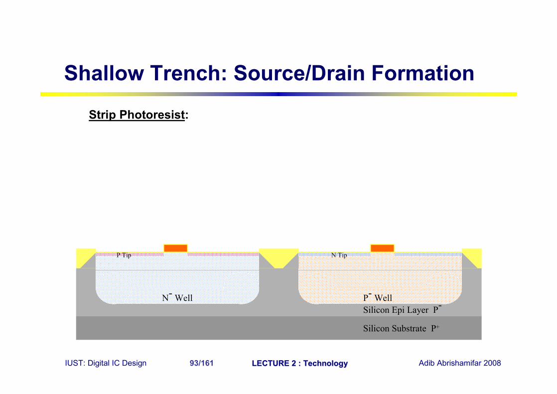
Strip Photoresist:
Silicon Substrate P+
Silicon Epi Layer P-P- WellN- Well
N TipP Tip
Shallow Trench: Source/Drain Formation

IUST: Digital IC Design LECTURE 2 : TechnologyLECTURE 2 : Technology Adib Abrishamifar 200894/161
Deposit Silicon Nitride Layer: Using Chemical Vapor Deposition to achieve a very conformal film. Thickness: 1200-1800Å
Silicon Substrate P+
Silicon Epi Layer P-P- WellN- Well
Silicon Nitride
Thinner Here
Thicker Here
N TipP Tip
P Tip
Shallow Trench: Source/Drain Formation
IUST: Digital IC Design LECTURE 2 : TechnologyLECTURE 2 : Technology Adib Abrishamifar 200895/161
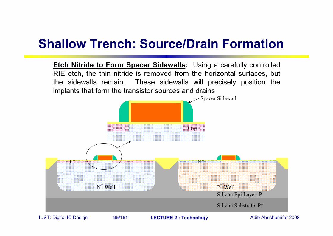
Etch Nitride to Form Spacer Sidewalls: Using a carefully controlled RIE etch, the thin nitride is removed from the horizontal surfaces, but the sidewalls remain. These sidewalls will precisely position the implants that form the transistor sources and drains
Silicon Substrate P+
Silicon Epi Layer P-P- WellN- Well
Spacer Sidewall
N TipP Tip
P Tip
Shallow Trench: Source/Drain Formation
IUST: Digital IC Design LECTURE 2 : TechnologyLECTURE 2 : Technology Adib Abrishamifar 200896/161
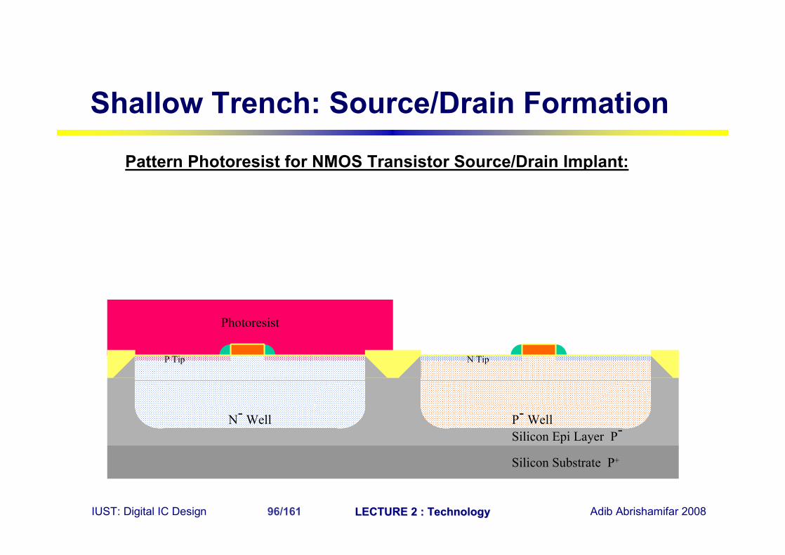
Pattern Photoresist for NMOS Transistor Source/Drain Implant:
Silicon Substrate P+
Silicon Epi Layer P-P- WellN- Well
Photoresist
N TipP Tip
Shallow Trench: Source/Drain Formation
IUST: Digital IC Design LECTURE 2 : TechnologyLECTURE 2 : Technology Adib Abrishamifar 200897/161
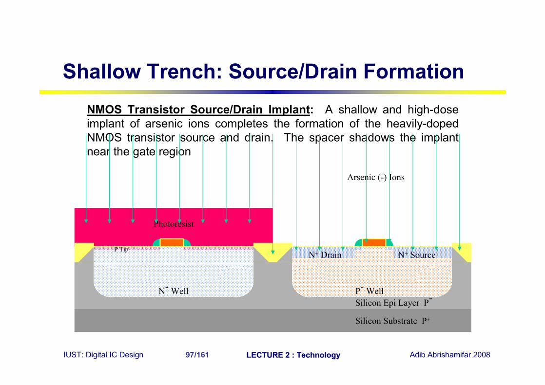
NMOS Transistor Source/Drain Implant: A shallow and high-dose implant of arsenic ions completes the formation of the heavily-doped NMOS transistor source and drain. The spacer shadows the implant near the gate region
Silicon Substrate P+
Silicon Epi Layer P-P- WellN- Well
Photoresist
Arsenic (-) Ions
N+ Drain N+ SourceP Tip
Shallow Trench: Source/Drain Formation
IUST: Digital IC Design LECTURE 2 : TechnologyLECTURE 2 : Technology Adib Abrishamifar 200898/161
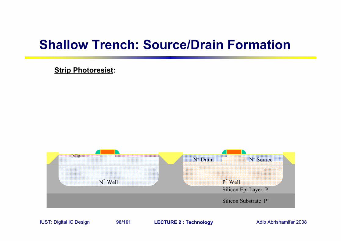
Strip Photoresist:
Silicon Substrate P+
Silicon Epi Layer P-P- WellN- Well
N+ Drain N+ SourceP Tip
Shallow Trench: Source/Drain Formation
IUST: Digital IC Design LECTURE 2 : TechnologyLECTURE 2 : Technology Adib Abrishamifar 200899/161
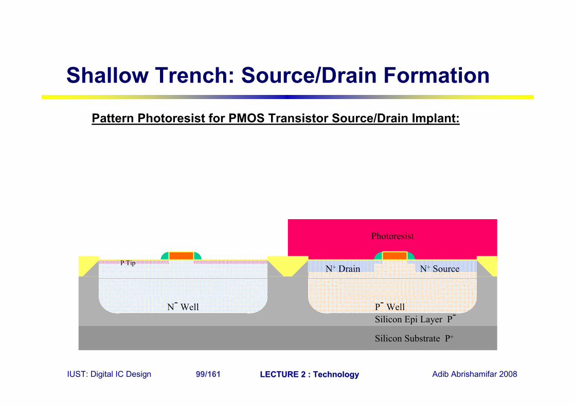
Pattern Photoresist for PMOS Transistor Source/Drain Implant:
Silicon Substrate P+
Silicon Epi Layer P-P- WellN- Well
N+ Drain N+ Source
Photoresist
P Tip
Shallow Trench: Source/Drain Formation
IUST: Digital IC Design LECTURE 2 : TechnologyLECTURE 2 : Technology Adib Abrishamifar 2008100/161
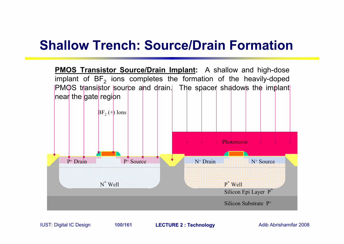
PMOS Transistor Source/Drain Implant: A shallow and high-dose implant of BF2 ions completes the formation of the heavily-doped PMOS transistor source and drain. The spacer shadows the implant near the gate region
Silicon Substrate P+
Silicon Epi Layer P-P- WellN- Well
BF2 (+) Ions
Photoresist
N+ Drain N+ SourceP+ SourceP+ Drain
Shallow Trench: Source/Drain Formation
IUST: Digital IC Design LECTURE 2 : TechnologyLECTURE 2 : Technology Adib Abrishamifar 2008101/161
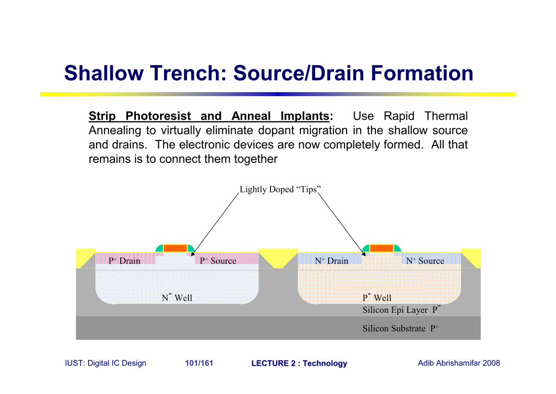
Strip Photoresist and Anneal Implants: Use Rapid Thermal Annealing to virtually eliminate dopant migration in the shallow source and drains. The electronic devices are now completely formed. All that remains is to connect them together
Silicon Substrate P+
Silicon Epi Layer P-P- WellN- Well
N+ Drain N+ SourceP+ SourceP+ Drain
Lightly Doped “Tips”
Shallow Trench: Source/Drain Formation
IUST: Digital IC Design LECTURE 2 : TechnologyLECTURE 2 : Technology Adib Abrishamifar 2008102/161
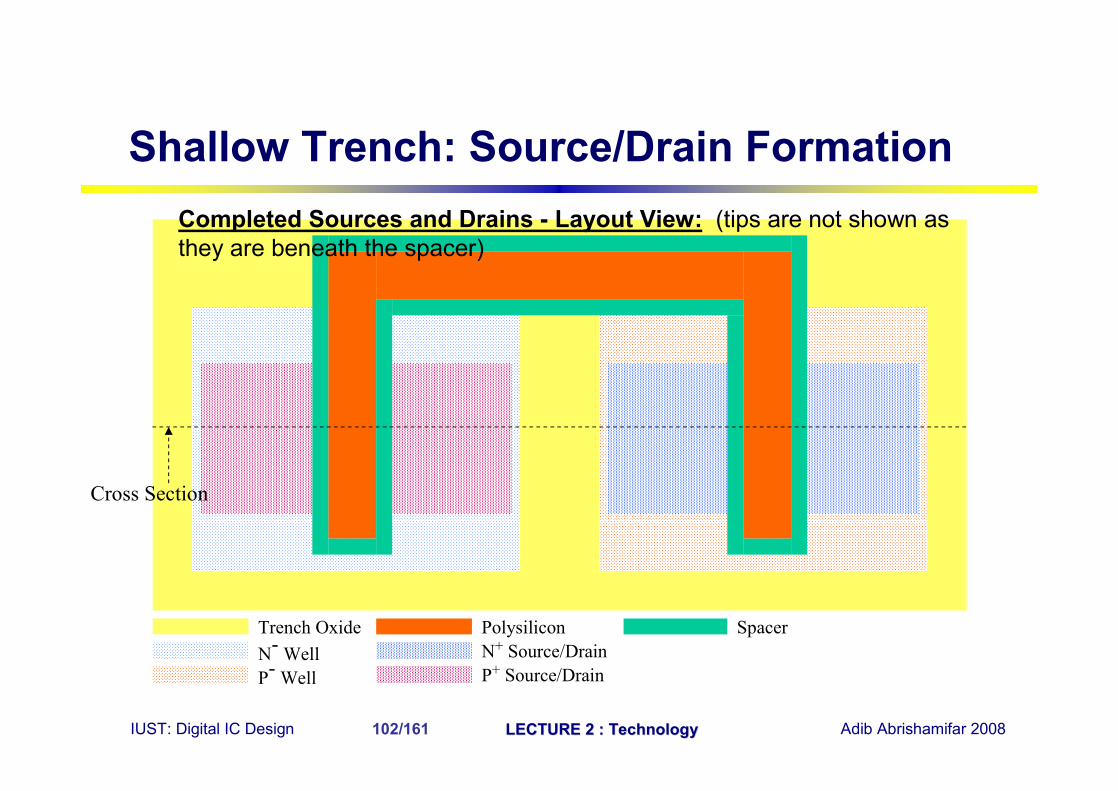
Trench Oxide Polysilicon
Cross Section
N- WellP- Well
N+ Source/DrainP+ Source/Drain
Spacer
Shallow Trench: Source/Drain FormationCompleted Sources and Drains - Layout View: (tips are not shown as they are beneath the spacer)
IUST: Digital IC Design LECTURE 2 : TechnologyLECTURE 2 : Technology Adib Abrishamifar 2008103/161
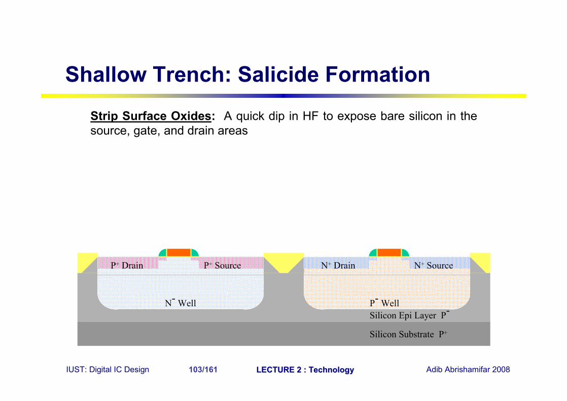
Strip Surface Oxides: A quick dip in HF to expose bare silicon in the source, gate, and drain areas
Silicon Substrate P+
Silicon Epi Layer P-P- WellN- Well
N+ Drain N+ SourceP+ Drain P+ Source
Shallow Trench: Salicide Formation
IUST: Digital IC Design LECTURE 2 : TechnologyLECTURE 2 : Technology Adib Abrishamifar 2008104/161
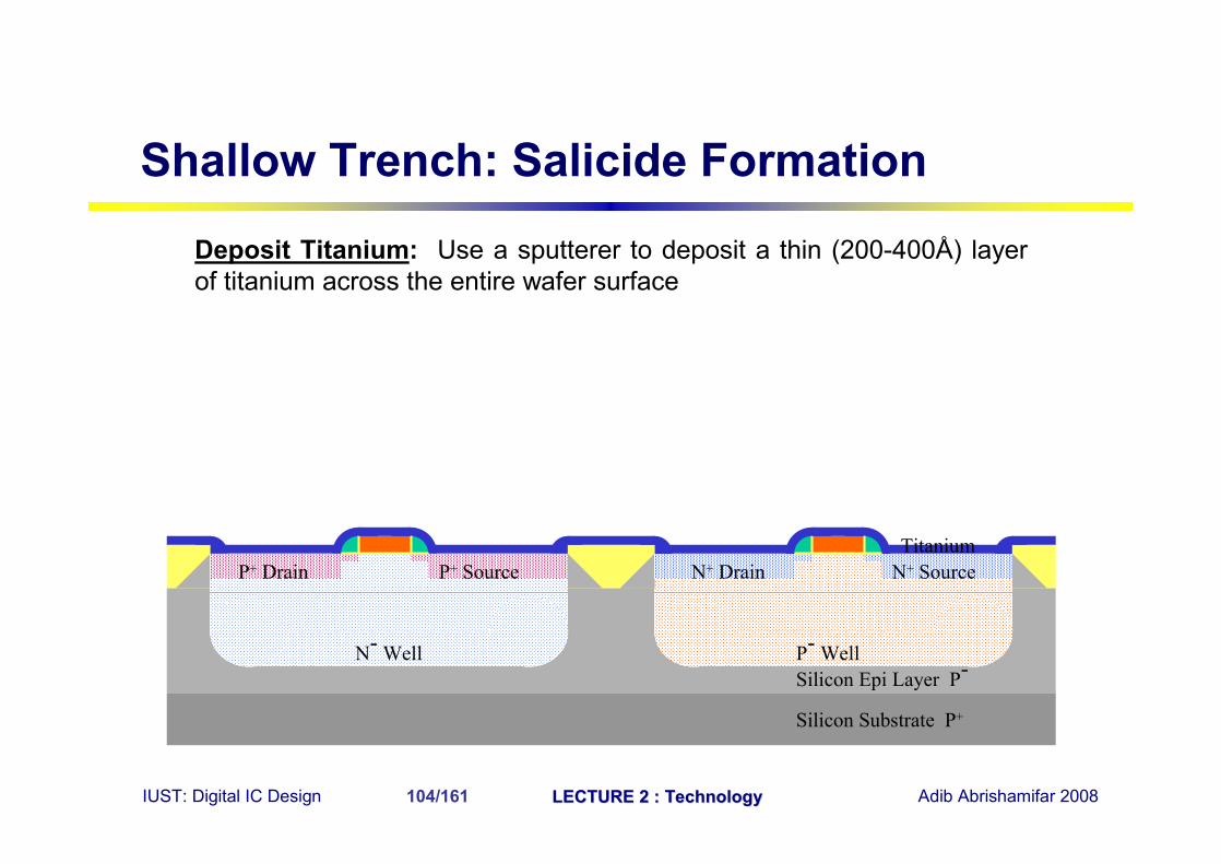
Deposit Titanium: Use a sputterer to deposit a thin (200-400Å) layer of titanium across the entire wafer surface
Silicon Substrate P+
Silicon Epi Layer P-P- WellN- Well
N+ Drain N+ SourceP+ Drain P+ SourceTitanium
Shallow Trench: Salicide Formation
IUST: Digital IC Design LECTURE 2 : TechnologyLECTURE 2 : Technology Adib Abrishamifar 2008105/161
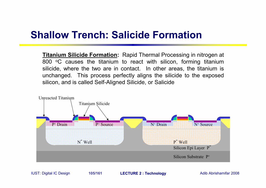
Titanium Silicide Formation: Rapid Thermal Processing in nitrogen at 800 oC causes the titanium to react with silicon, forming titanium silicide, where the two are in contact. In other areas, the titanium isunchanged. This process perfectly aligns the silicide to the exposed silicon, and is called Self-Aligned Silicide, or Salicide
Silicon Substrate P+
Silicon Epi Layer P-P- WellN- Well
N+ Drain N+ SourceP+ Drain P+ Source
Titanium SilicideUnreacted Titanium
Shallow Trench: Salicide Formation
IUST: Digital IC Design LECTURE 2 : TechnologyLECTURE 2 : Technology Adib Abrishamifar 2008106/161
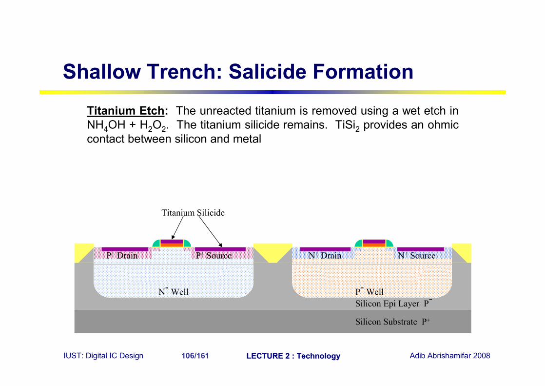
Titanium Etch: The unreacted titanium is removed using a wet etch in NH4OH + H2O2. The titanium silicide remains. TiSi2 provides an ohmiccontact between silicon and metal
Silicon Substrate P+
Silicon Epi Layer P-P- WellN- Well
N+ Drain N+ SourceP+ Drain P+ Source
Titanium Silicide
Shallow Trench: Salicide Formation
IUST: Digital IC Design LECTURE 2 : TechnologyLECTURE 2 : Technology Adib Abrishamifar 2008107/161
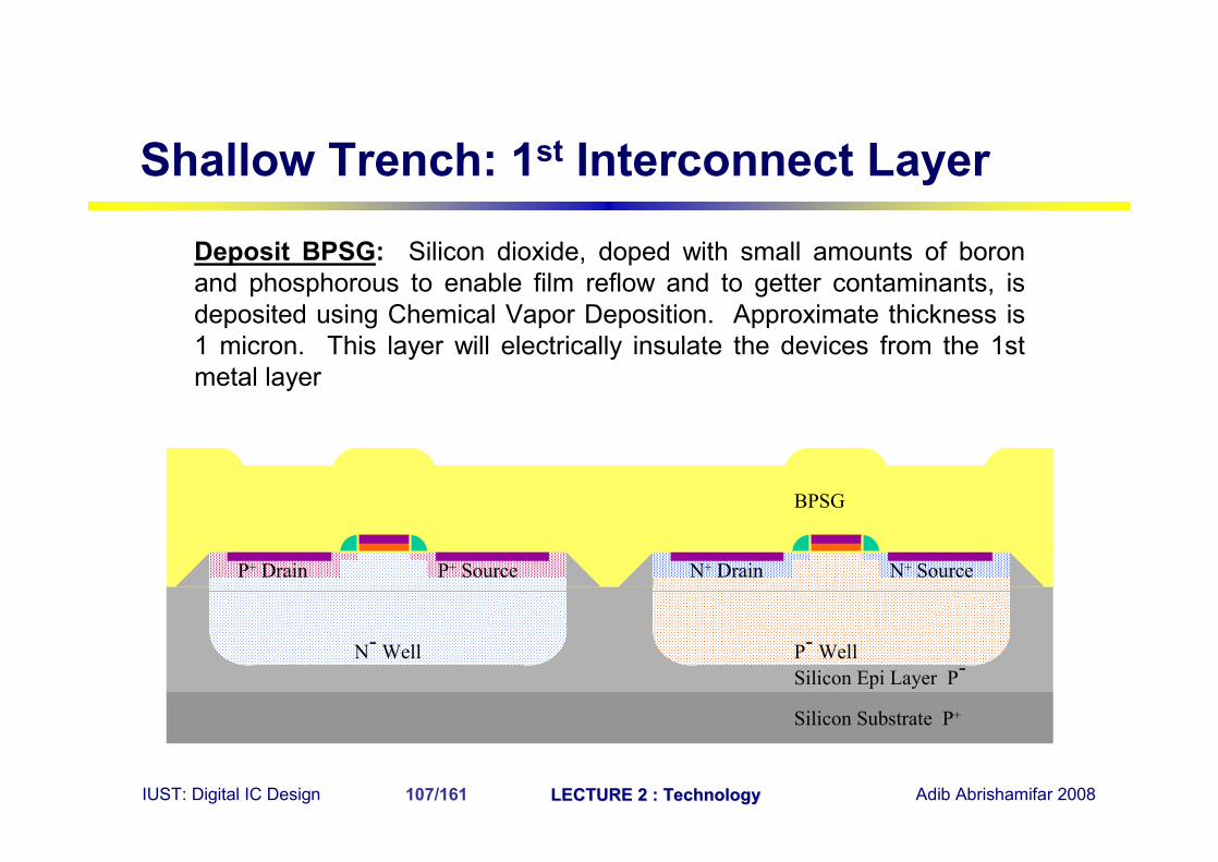
Deposit BPSG: Silicon dioxide, doped with small amounts of boron and phosphorous to enable film reflow and to getter contaminants, is deposited using Chemical Vapor Deposition. Approximate thickness is 1 micron. This layer will electrically insulate the devices from the 1st metal layer
Silicon Substrate P+
Silicon Epi Layer P-P- WellN- Well
N+ Drain N+ SourceP+ Drain P+ Source
BPSG
Shallow Trench: 1st Interconnect Layer

IUST: Digital IC Design LECTURE 2 : TechnologyLECTURE 2 : Technology Adib Abrishamifar 2008108/161
Polish BPSG: Use Chemical Mechanical Polishing to achieve a flat surface on the BPSG layer. If not removed, the bumps on the surface from the underlying topography would cause focus problems for the subsequent photolithography steps and degrade metal step coverage
Silicon Substrate P+
Silicon Epi Layer P-P- WellN- Well
N+ Drain N+ SourceP+ Drain P+ Source
BPSG
Shallow Trench: 1st Interconnect Layer
IUST: Digital IC Design LECTURE 2 : TechnologyLECTURE 2 : Technology Adib Abrishamifar 2008109/161
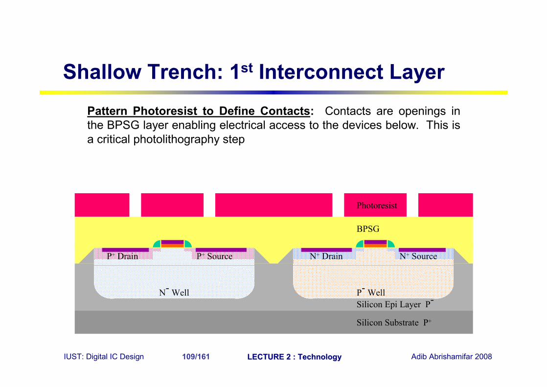
Pattern Photoresist to Define Contacts: Contacts are openings in the BPSG layer enabling electrical access to the devices below. This is a critical photolithography step
Silicon Substrate P+
Silicon Epi Layer P-P- WellN- Well
N+ Drain N+ SourceP+ Drain P+ Source
BPSG
Photoresist
Shallow Trench: 1st Interconnect Layer
IUST: Digital IC Design LECTURE 2 : TechnologyLECTURE 2 : Technology Adib Abrishamifar 2008110/161
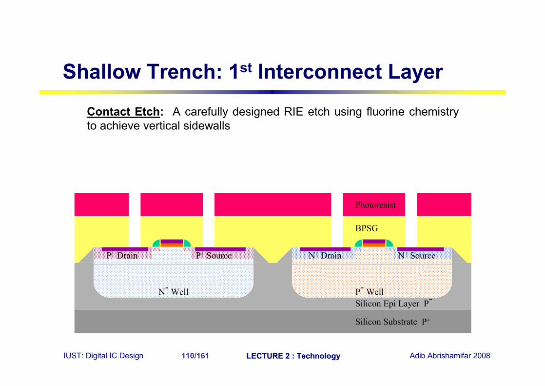
Contact Etch: A carefully designed RIE etch using fluorine chemistry to achieve vertical sidewalls
Silicon Substrate P+
Silicon Epi Layer P-P- WellN- Well
N+ Drain N+ SourceP+ Drain P+ Source
BPSG
Photoresist
Shallow Trench: 1st Interconnect Layer
IUST: Digital IC Design LECTURE 2 : TechnologyLECTURE 2 : Technology Adib Abrishamifar 2008111/161
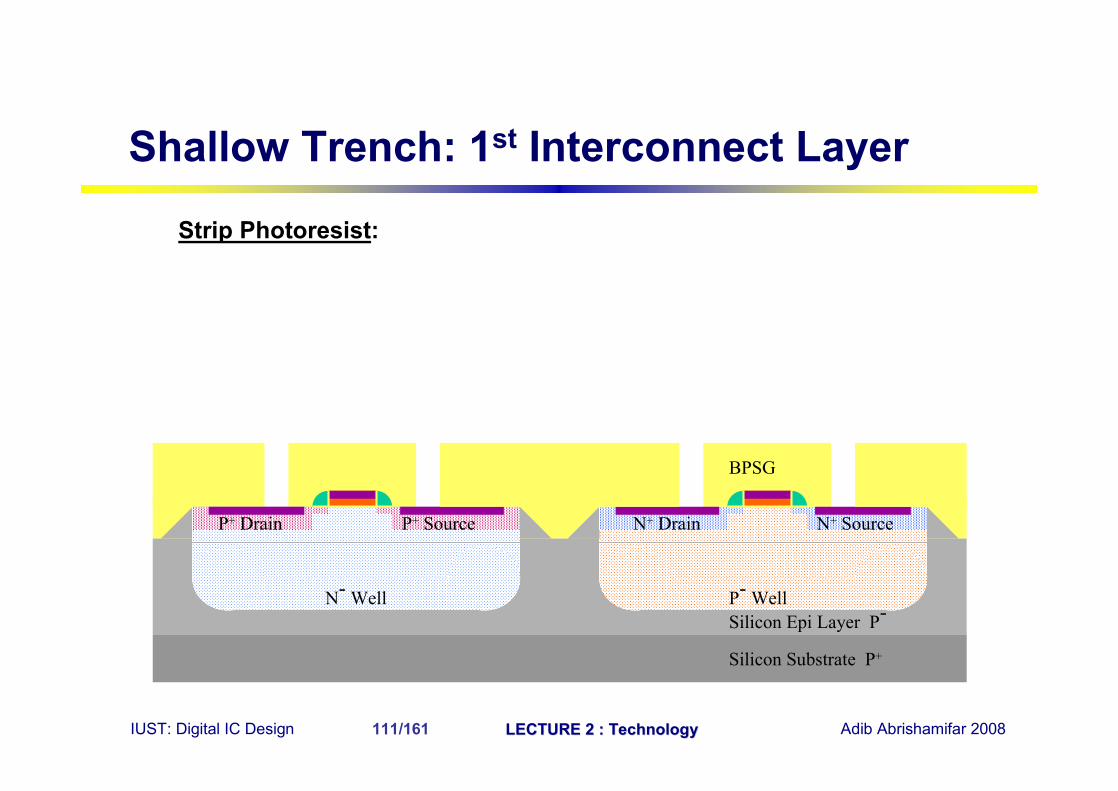
Strip Photoresist:
Silicon Substrate P+
Silicon Epi Layer P-P- WellN- Well
N+ Drain N+ SourceP+ Drain P+ Source
BPSG
Shallow Trench: 1st Interconnect Layer
IUST: Digital IC Design LECTURE 2 : TechnologyLECTURE 2 : Technology Adib Abrishamifar 2008112/161
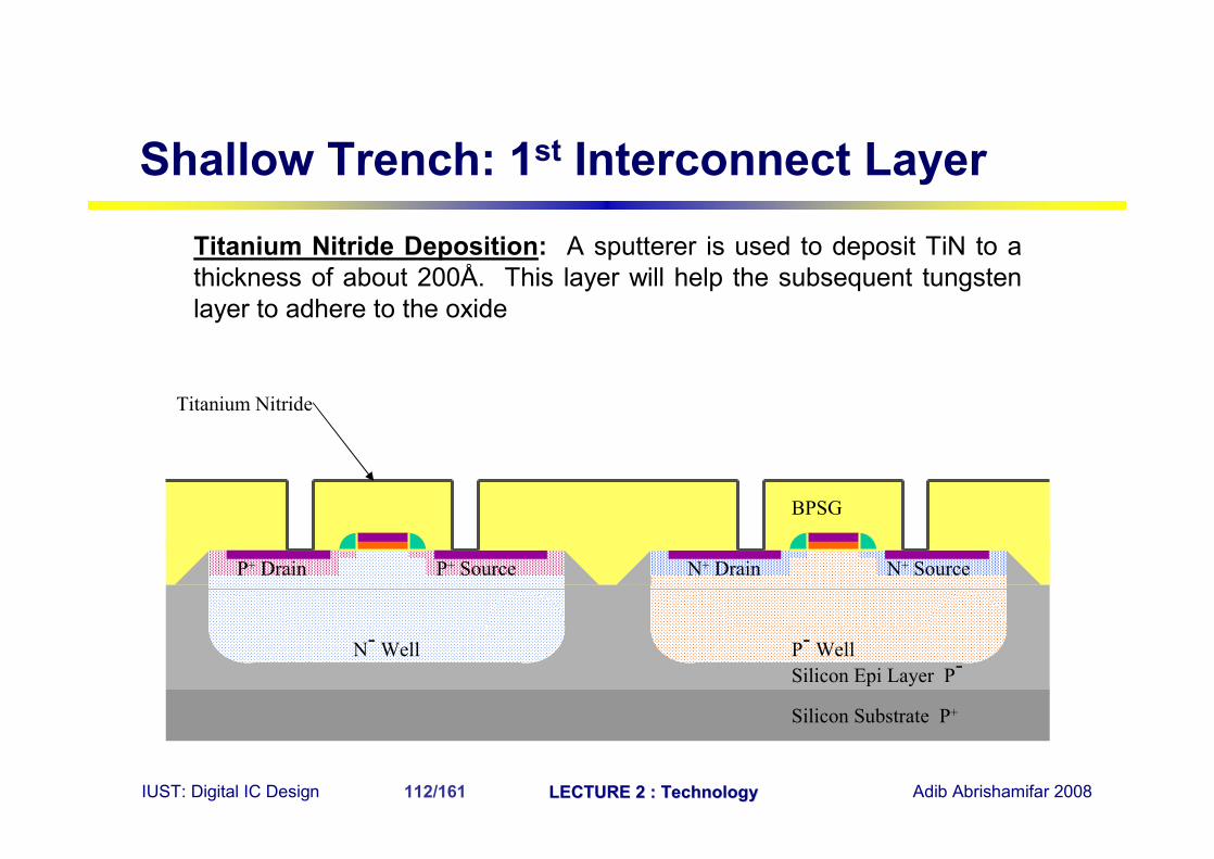
Titanium Nitride Deposition: A sputterer is used to deposit TiN to a thickness of about 200Å. This layer will help the subsequent tungsten layer to adhere to the oxide
Silicon Substrate P+
Silicon Epi Layer P-P- WellN- Well
N+ Drain N+ SourceP+ Drain P+ Source
BPSG
Titanium Nitride
Shallow Trench: 1st Interconnect Layer
IUST: Digital IC Design LECTURE 2 : TechnologyLECTURE 2 : Technology Adib Abrishamifar 2008113/161
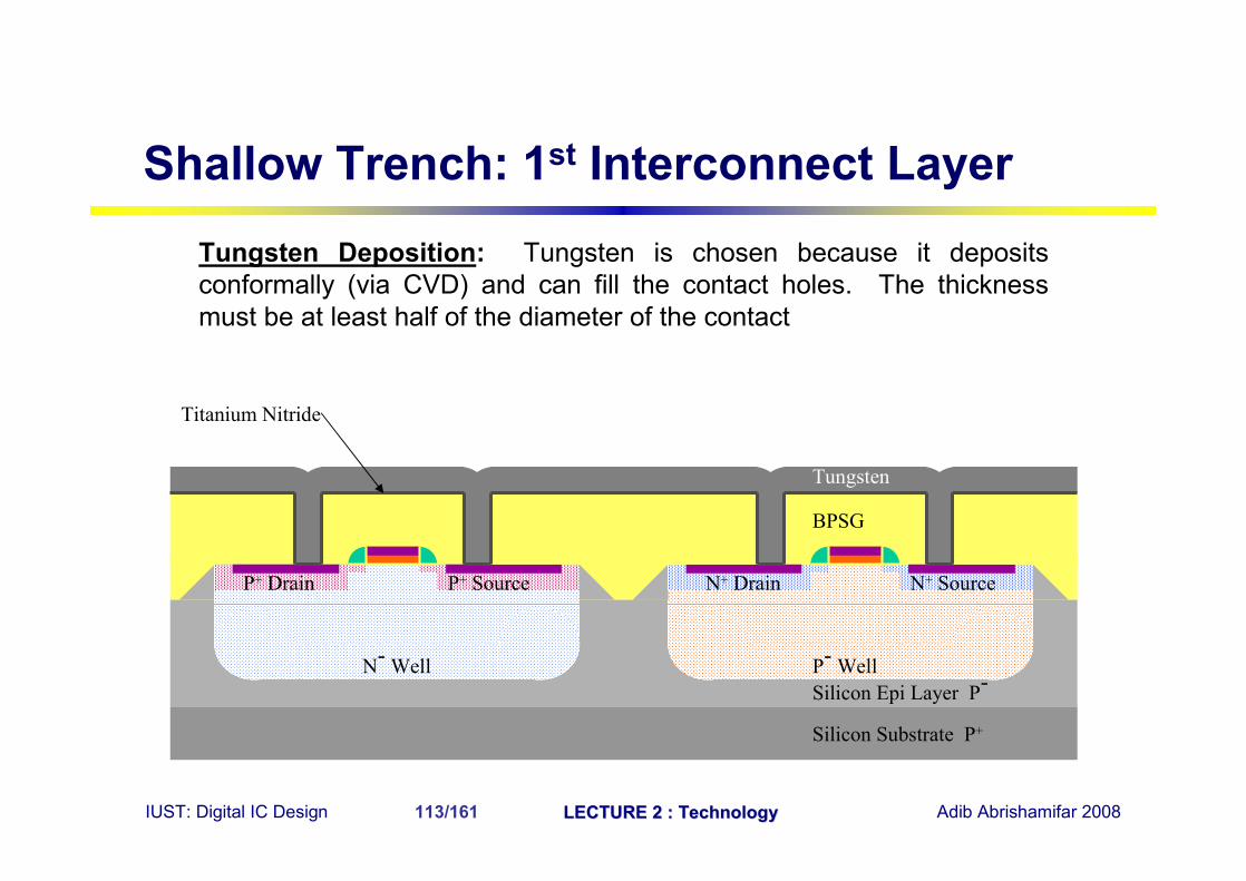
Tungsten Deposition: Tungsten is chosen because it deposits conformally (via CVD) and can fill the contact holes. The thickness must be at least half of the diameter of the contact
Silicon Substrate P+
Silicon Epi Layer P-P- WellN- Well
N+ Drain N+ SourceP+ Drain P+ Source
BPSG
Titanium Nitride
Tungsten
Shallow Trench: 1st Interconnect Layer
IUST: Digital IC Design LECTURE 2 : TechnologyLECTURE 2 : Technology Adib Abrishamifar 2008114/161
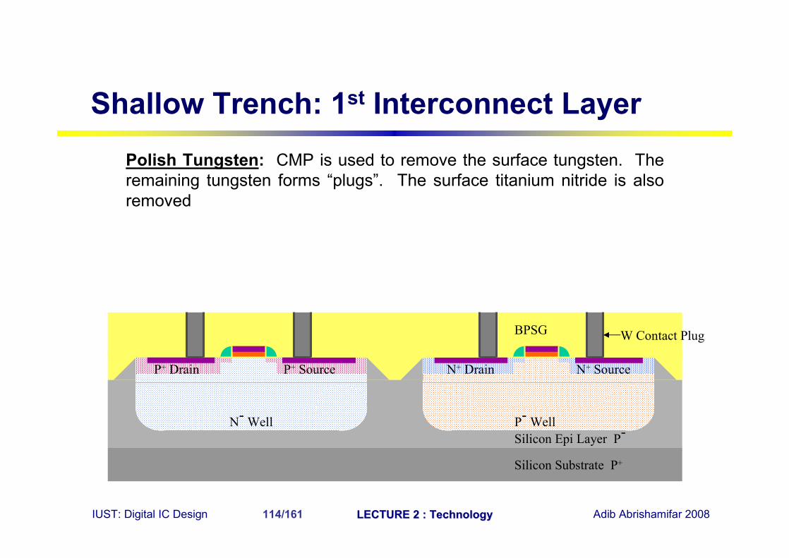
Polish Tungsten: CMP is used to remove the surface tungsten. The remaining tungsten forms “plugs”. The surface titanium nitride is also removed
Silicon Substrate P+
Silicon Epi Layer P-P- WellN- Well
N+ Drain N+ SourceP+ Drain P+ Source
BPSG W Contact Plug
Shallow Trench: 1st Interconnect Layer
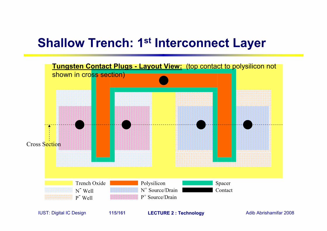
IUST: Digital IC Design LECTURE 2 : TechnologyLECTURE 2 : Technology Adib Abrishamifar 2008115/161
Trench Oxide Polysilicon
Cross Section
N- WellP- Well
N+ Source/DrainP+ Source/Drain
SpacerContact
Shallow Trench: 1st Interconnect LayerTungsten Contact Plugs - Layout View: (top contact to polysilicon not shown in cross section)
IUST: Digital IC Design LECTURE 2 : TechnologyLECTURE 2 : Technology Adib Abrishamifar 2008116/161
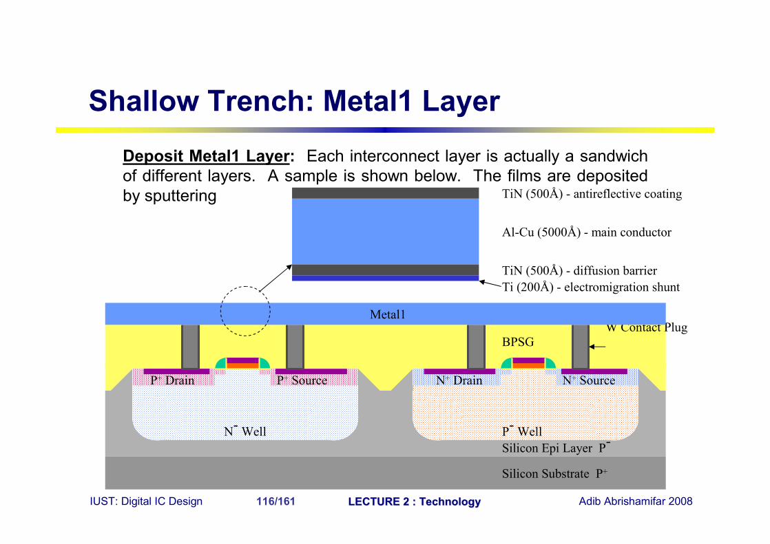
Deposit Metal1 Layer: Each interconnect layer is actually a sandwich of different layers. A sample is shown below. The films are deposited by sputtering
Silicon Substrate P+
Silicon Epi Layer P-P- WellN- Well
N+ Drain N+ SourceP+ Drain P+ Source
BPSGW Contact Plug
Metal1
Ti (200Å) - electromigration shuntTiN (500Å) - diffusion barrier
Al-Cu (5000Å) - main conductor
TiN (500Å) - antireflective coating
Shallow Trench: Metal1 Layer
IUST: Digital IC Design LECTURE 2 : TechnologyLECTURE 2 : Technology Adib Abrishamifar 2008117/161
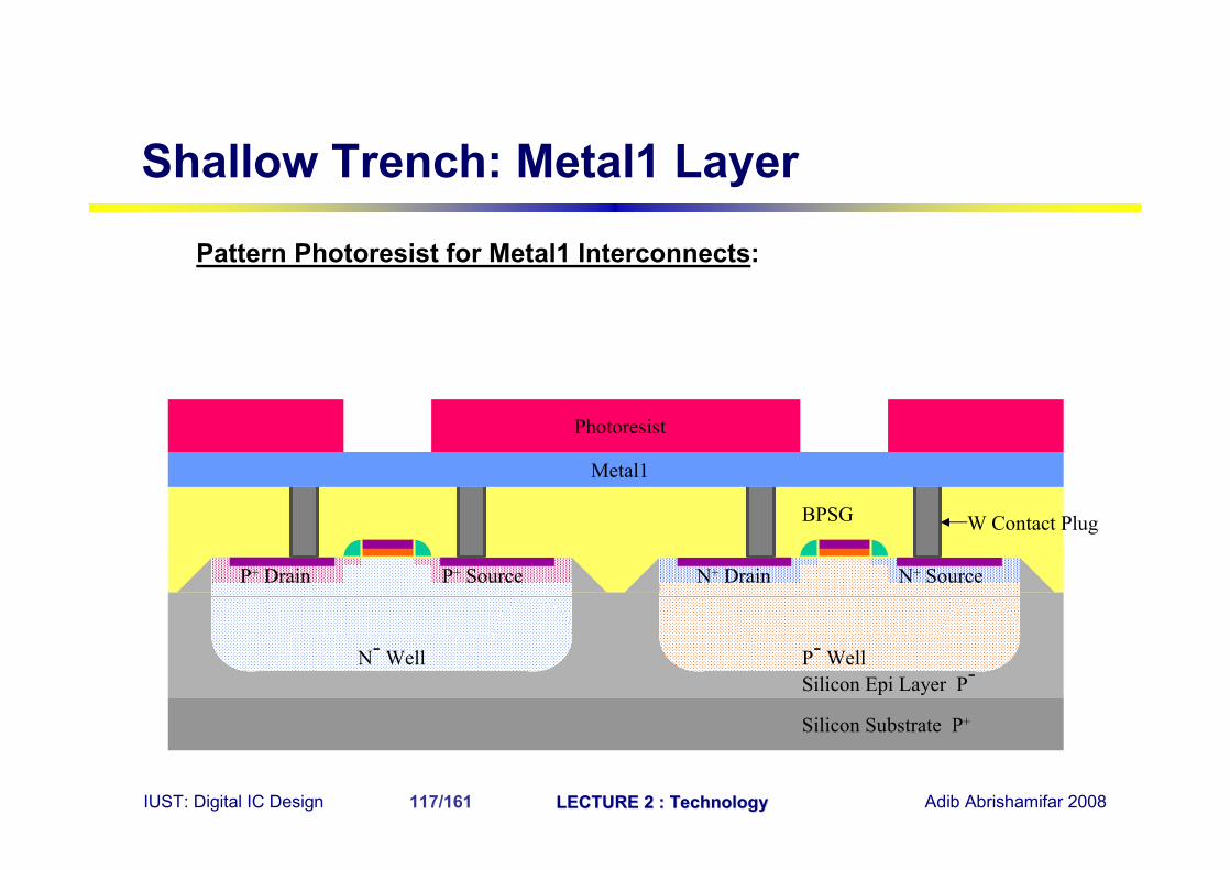
Pattern Photoresist for Metal1 Interconnects:
Silicon Substrate P+
Silicon Epi Layer P-P- WellN- Well
N+ Drain N+ SourceP+ Drain P+ Source
BPSG W Contact Plug
Metal1
Photoresist
Shallow Trench: Metal1 Layer
IUST: Digital IC Design LECTURE 2 : TechnologyLECTURE 2 : Technology Adib Abrishamifar 2008118/161
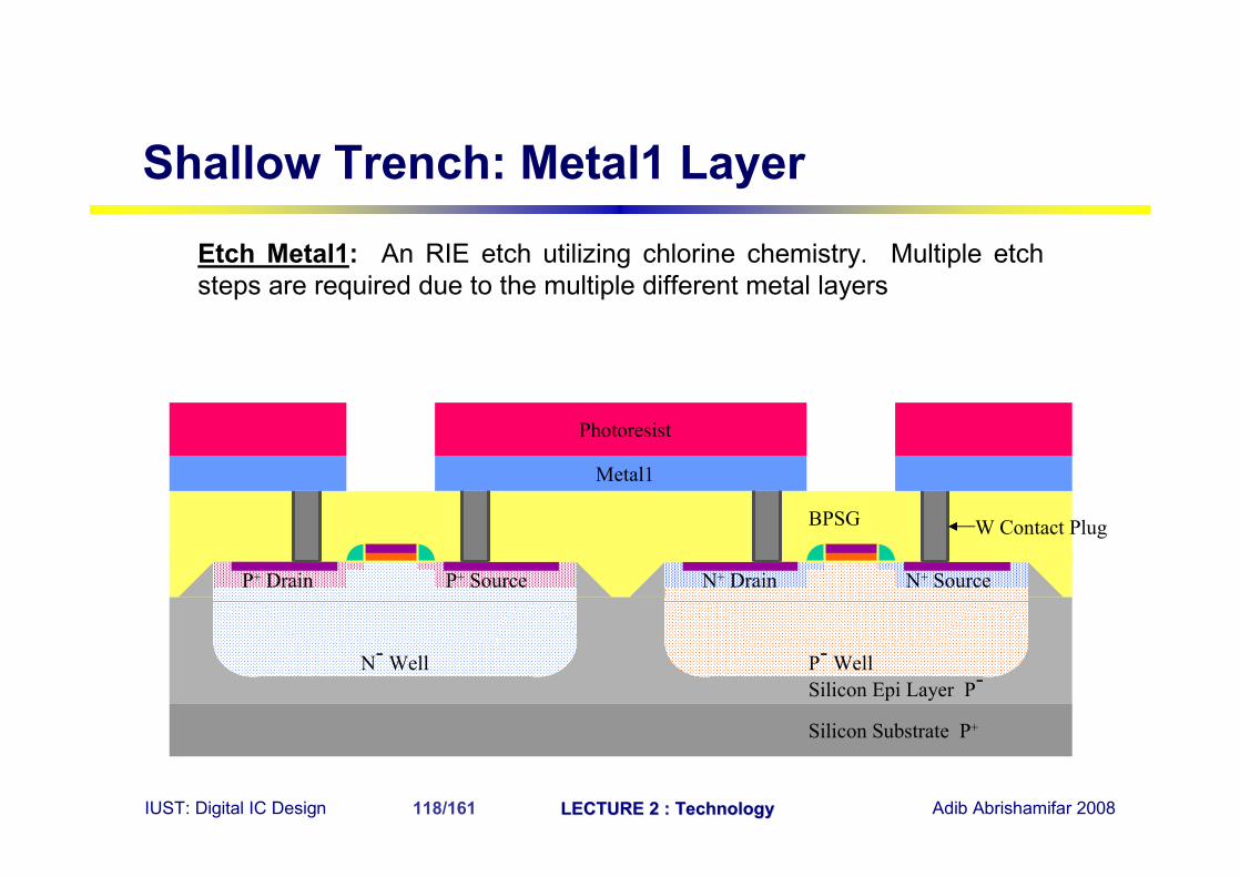
Etch Metal1: An RIE etch utilizing chlorine chemistry. Multiple etch steps are required due to the multiple different metal layers
Silicon Substrate P+
Silicon Epi Layer P-P- WellN- Well
N+ Drain N+ SourceP+ Drain P+ Source
BPSG W Contact Plug
Metal1
Photoresist
Shallow Trench: Metal1 Layer
IUST: Digital IC Design LECTURE 2 : TechnologyLECTURE 2 : Technology Adib Abrishamifar 2008119/161
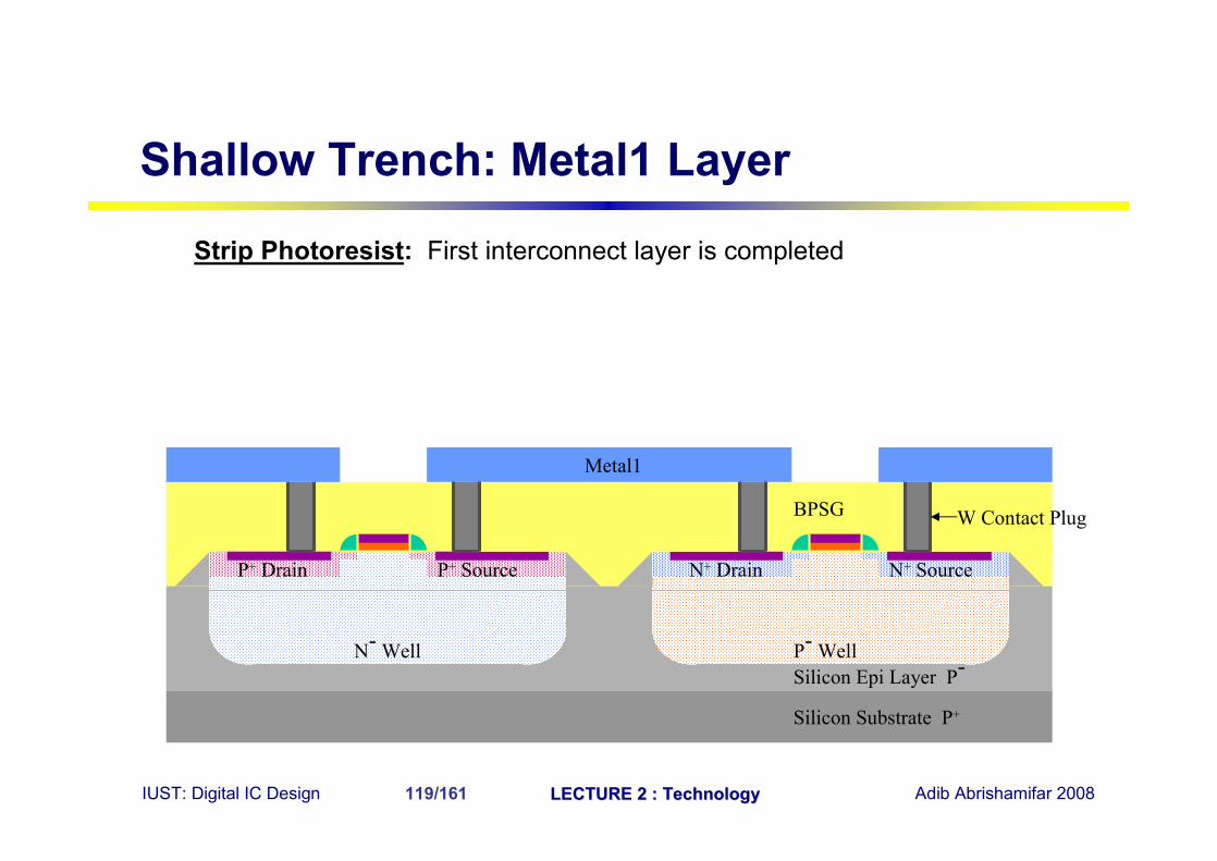
Strip Photoresist: First interconnect layer is completed
Silicon Substrate P+
Silicon Epi Layer P-P- WellN- Well
N+ Drain N+ SourceP+ Drain P+ Source
BPSG W Contact Plug
Metal1
Shallow Trench: Metal1 Layer
IUST: Digital IC Design LECTURE 2 : TechnologyLECTURE 2 : Technology Adib Abrishamifar 2008120/161
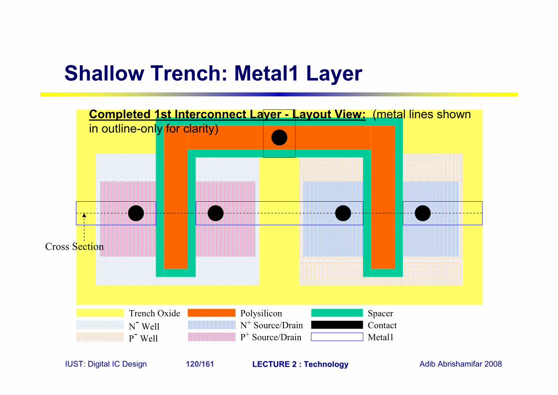
Trench Oxide Polysilicon
Cross Section
N- WellP- Well
N+ Source/DrainP+ Source/Drain
SpacerContactMetal1
Shallow Trench: Metal1 Layer
Completed 1st Interconnect Layer - Layout View: (metal lines shown in outline-only for clarity)
IUST: Digital IC Design LECTURE 2 : TechnologyLECTURE 2 : Technology Adib Abrishamifar 2008121/161
Silicon Substrate P+
Silicon Epi Layer P-P- WellN- Well
N+ Drain N+ SourceP+ Drain P+ Source
BPSG W Contact Plug
Metal1
IMD1
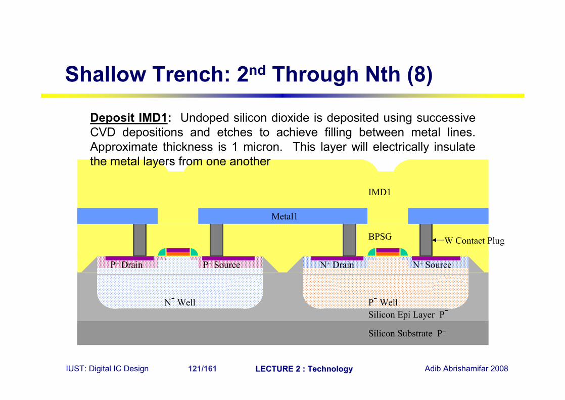
Shallow Trench: 2nd Through Nth (8)
Deposit IMD1: Undoped silicon dioxide is deposited using successive CVD depositions and etches to achieve filling between metal lines. Approximate thickness is 1 micron. This layer will electrically insulate the metal layers from one another

IUST: Digital IC Design LECTURE 2 : TechnologyLECTURE 2 : Technology Adib Abrishamifar 2008122/161
Polish IMD1: Use Chemical Mechanical Polishing to achieve a flat surface on the IMD layer. If not removed, the bumps on the surface from the underlying topography would cause focus problems for the subsequent photolithography steps and degrade metal step coverage
Silicon Substrate P+
Silicon Epi Layer P-P- WellN- Well
N+ Drain N+ SourceP+ Drain P+ Source
BPSG W Contact Plug
Metal1
IMD1
Shallow Trench: 2nd Through Nth (8)
IUST: Digital IC Design LECTURE 2 : TechnologyLECTURE 2 : Technology Adib Abrishamifar 2008123/161
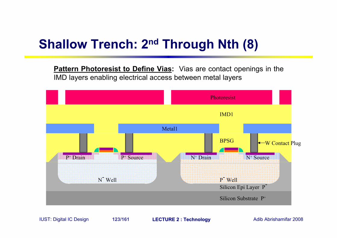
Pattern Photoresist to Define Vias: Vias are contact openings in the IMD layers enabling electrical access between metal layers
Silicon Substrate P+
Silicon Epi Layer P-P- WellN- Well
N+ Drain N+ SourceP+ Drain P+ Source
BPSG W Contact Plug
Metal1
IMD1
Photoresist
Shallow Trench: 2nd Through Nth (8)
IUST: Digital IC Design LECTURE 2 : TechnologyLECTURE 2 : Technology Adib Abrishamifar 2008124/161
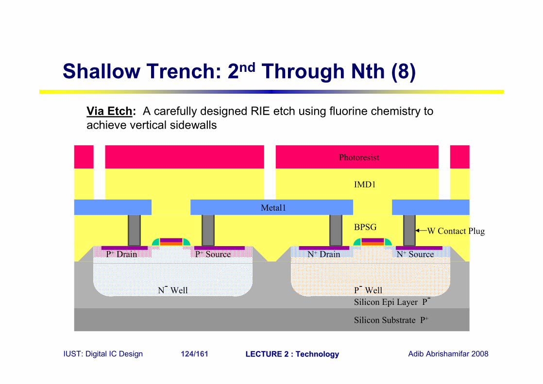
Via Etch: A carefully designed RIE etch using fluorine chemistry to achieve vertical sidewalls
Silicon Substrate P+
Silicon Epi Layer P-P- WellN- Well
N+ Drain N+ SourceP+ Drain P+ Source
BPSG W Contact Plug
Metal1
Photoresist
IMD1
Shallow Trench: 2nd Through Nth (8)
IUST: Digital IC Design LECTURE 2 : TechnologyLECTURE 2 : Technology Adib Abrishamifar 2008125/161
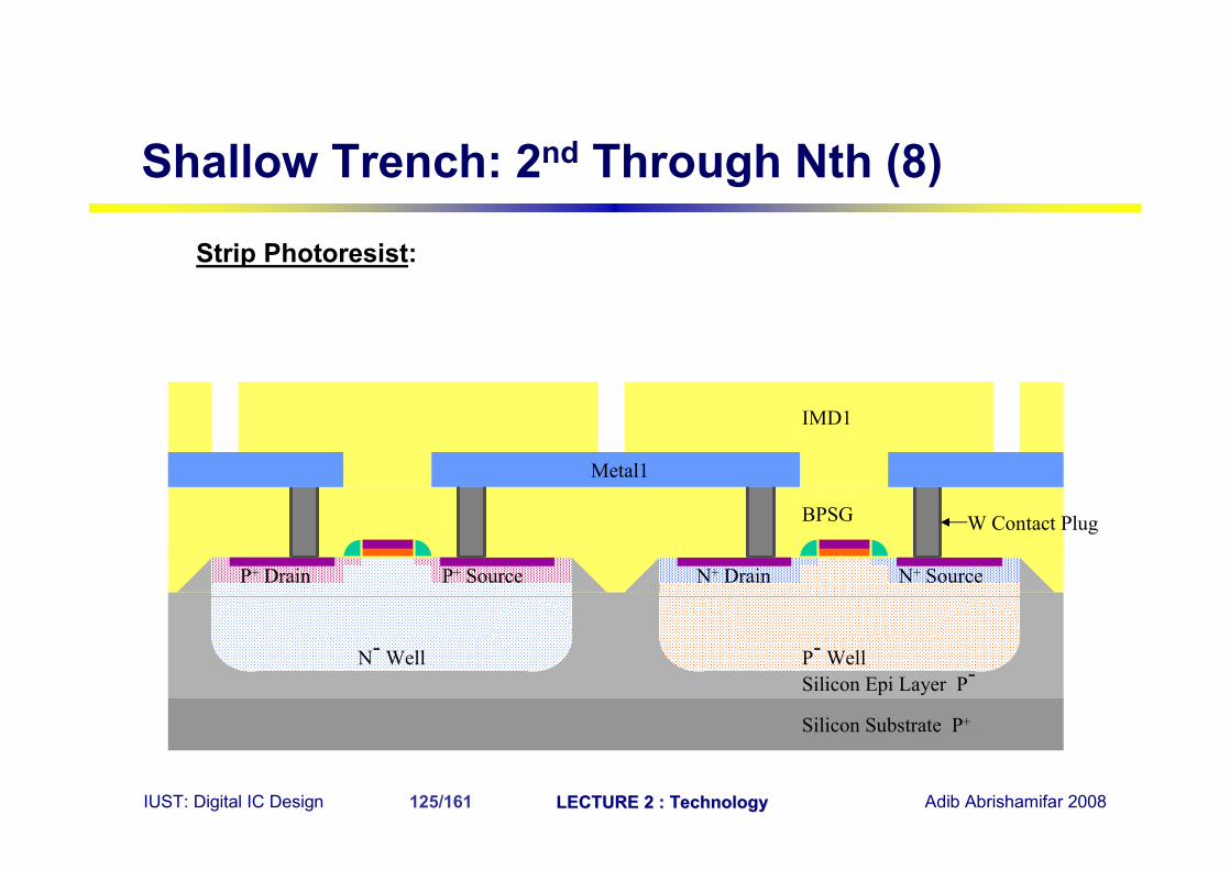
Strip Photoresist:
Silicon Substrate P+
Silicon Epi Layer P-P- WellN- Well
N+ Drain N+ SourceP+ Drain P+ Source
BPSG W Contact Plug
Metal1
IMD1
Shallow Trench: 2nd Through Nth (8)
IUST: Digital IC Design LECTURE 2 : TechnologyLECTURE 2 : Technology Adib Abrishamifar 2008126/161
Tungsten
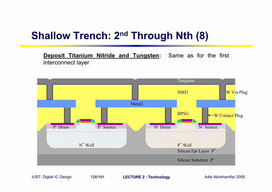
Deposit Titanium Nitride and Tungsten: Same as for the first interconnect layer
Silicon Substrate P+
Silicon Epi Layer P-P- WellN- Well
N+ Drain N+ SourceP+ Drain P+ Source
BPSG W Contact Plug
Metal1
IMD1 W Via Plug
Shallow Trench: 2nd Through Nth (8)
IUST: Digital IC Design LECTURE 2 : TechnologyLECTURE 2 : Technology Adib Abrishamifar 2008127/161
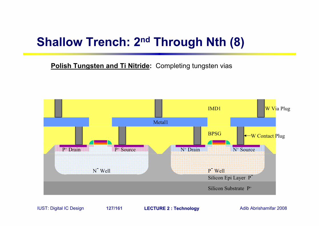
Polish Tungsten and Ti Nitride: Completing tungsten vias
Silicon Substrate P+
Silicon Epi Layer P-P- WellN- Well
N+ Drain N+ SourceP+ Drain P+ Source
BPSG W Contact Plug
Metal1
IMD1 W Via Plug
Shallow Trench: 2nd Through Nth (8)
IUST: Digital IC Design LECTURE 2 : TechnologyLECTURE 2 : Technology Adib Abrishamifar 2008128/161
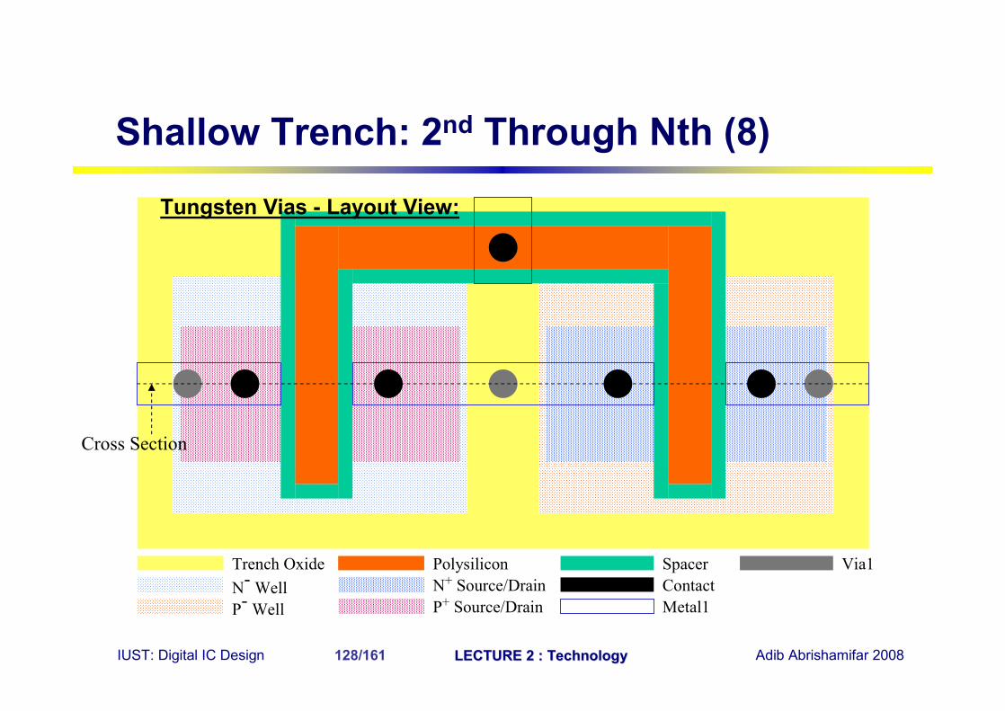
Trench Oxide Polysilicon
Cross Section
N- WellP- Well
N+ Source/DrainP+ Source/Drain
SpacerContactMetal1
Via1
Shallow Trench: 2nd Through Nth (8)
Tungsten Vias - Layout View:
IUST: Digital IC Design LECTURE 2 : TechnologyLECTURE 2 : Technology Adib Abrishamifar 2008129/161
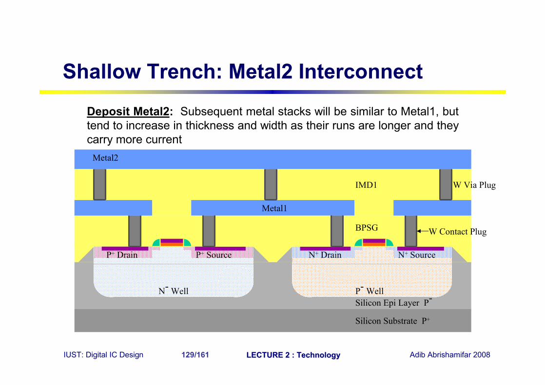
Deposit Metal2: Subsequent metal stacks will be similar to Metal1, but tend to increase in thickness and width as their runs are longer and they carry more current
Silicon Substrate P+
Silicon Epi Layer P-P- WellN- Well
N+ Drain N+ SourceP+ Drain P+ Source
BPSG W Contact Plug
Metal1
IMD1 W Via Plug
Metal2
Shallow Trench: Metal2 Interconnect
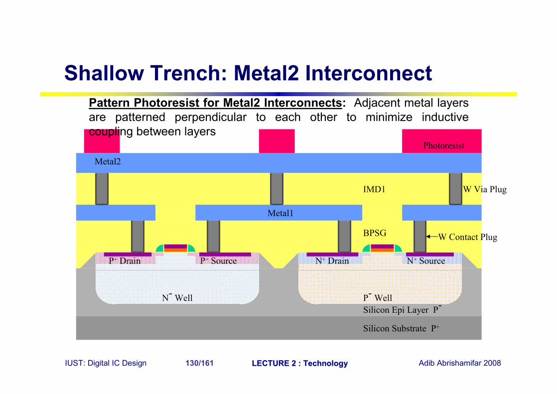
IUST: Digital IC Design LECTURE 2 : TechnologyLECTURE 2 : Technology Adib Abrishamifar 2008130/161
Silicon Substrate P+
Silicon Epi Layer P-P- WellN- Well
N+ Drain N+ SourceP+ Drain P+ Source
BPSG W Contact Plug
Metal1
Photoresist
IMD1 W Via Plug
Metal2
Shallow Trench: Metal2 InterconnectPattern Photoresist for Metal2 Interconnects: Adjacent metal layers are patterned perpendicular to each other to minimize inductive coupling between layers
IUST: Digital IC Design LECTURE 2 : TechnologyLECTURE 2 : Technology Adib Abrishamifar 2008131/161
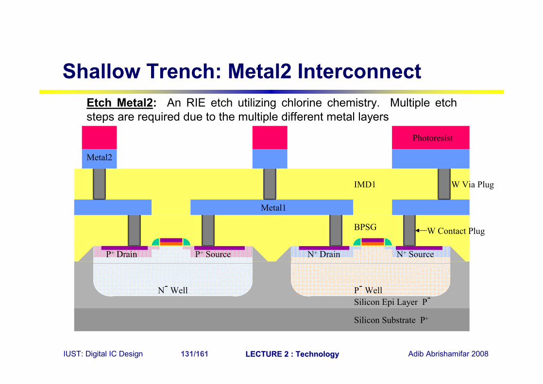
Etch Metal2: An RIE etch utilizing chlorine chemistry. Multiple etch steps are required due to the multiple different metal layers
Silicon Substrate P+
Silicon Epi Layer P-P- WellN- Well
N+ Drain N+ SourceP+ Drain P+ Source
BPSG W Contact Plug
Metal1
Photoresist
IMD1 W Via Plug
Metal2
Shallow Trench: Metal2 Interconnect
IUST: Digital IC Design LECTURE 2 : TechnologyLECTURE 2 : Technology Adib Abrishamifar 2008132/161
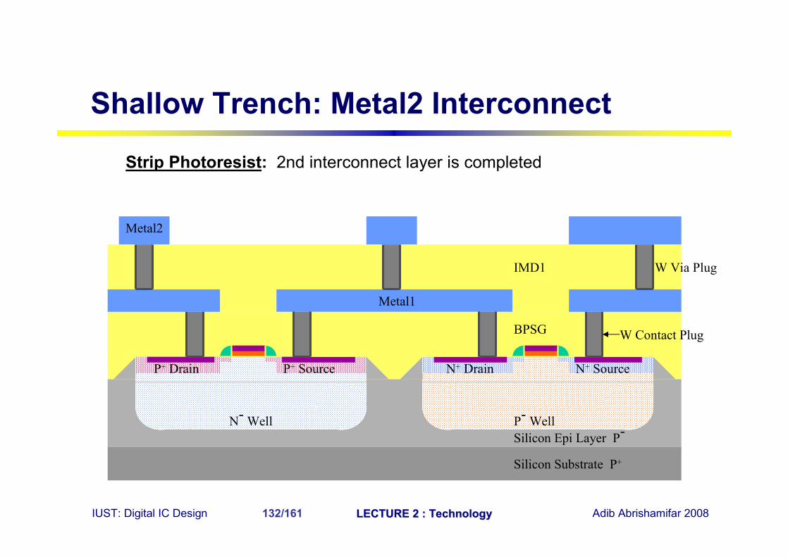
Strip Photoresist: 2nd interconnect layer is completed
Silicon Substrate P+
Silicon Epi Layer P-P- WellN- Well
N+ Drain N+ SourceP+ Drain P+ Source
BPSG W Contact Plug
Metal1
IMD1 W Via Plug
Metal2
Shallow Trench: Metal2 Interconnect
IUST: Digital IC Design LECTURE 2 : TechnologyLECTURE 2 : Technology Adib Abrishamifar 2008133/161
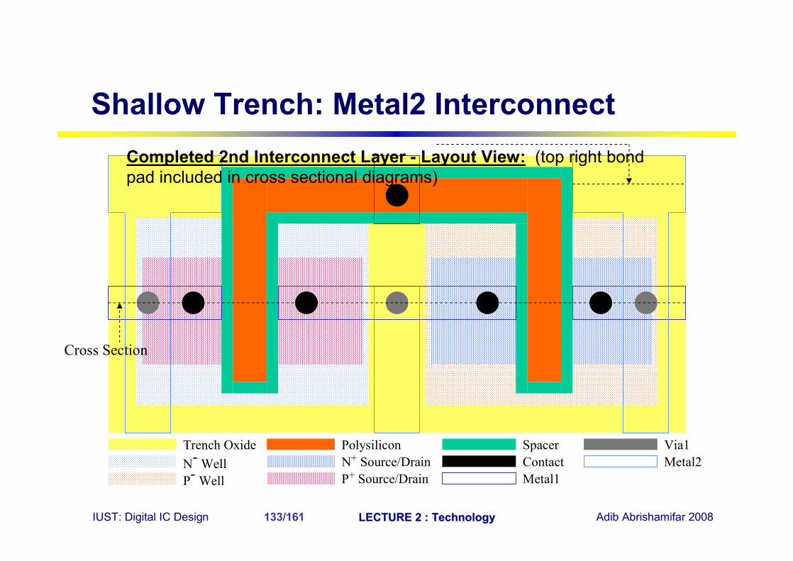
Trench Oxide Polysilicon
Cross Section
N- WellP- Well
N+ Source/DrainP+ Source/Drain
SpacerContactMetal1
Via1Metal2
Shallow Trench: Metal2 InterconnectCompleted 2nd Interconnect Layer - Layout View: (top right bond pad included in cross sectional diagrams)
IUST: Digital IC Design LECTURE 2 : TechnologyLECTURE 2 : Technology Adib Abrishamifar 2008134/161
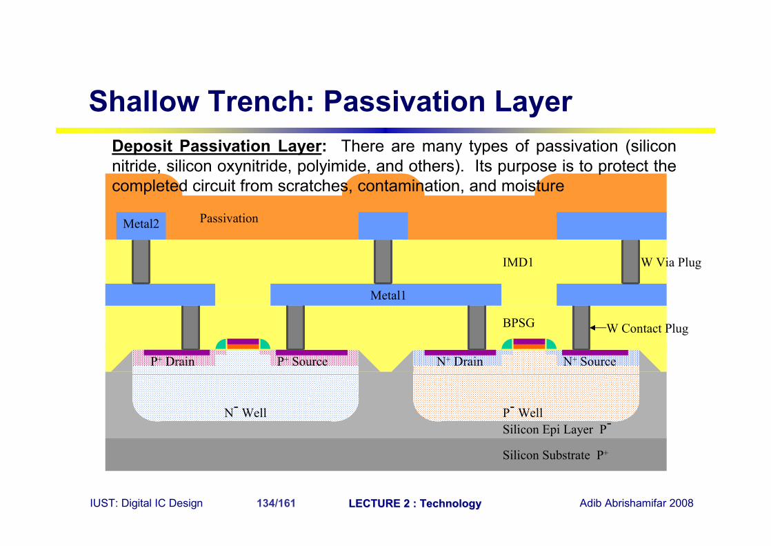
Silicon Substrate P+
Silicon Epi Layer P-P- WellN- Well
N+ Drain N+ SourceP+ Drain P+ Source
BPSG W Contact Plug
Metal1
IMD1 W Via Plug
PassivationMetal2
Shallow Trench: Passivation LayerDeposit Passivation Layer: There are many types of passivation (silicon nitride, silicon oxynitride, polyimide, and others). Its purpose is to protect the completed circuit from scratches, contamination, and moisture
IUST: Digital IC Design LECTURE 2 : TechnologyLECTURE 2 : Technology Adib Abrishamifar 2008135/161
Silicon Substrate P+
Silicon Epi Layer P-P- WellN- Well
N+ Drain N+ SourceP+ Drain P+ Source
BPSG W Contact Plug
Metal1
IMD1 W Via Plug
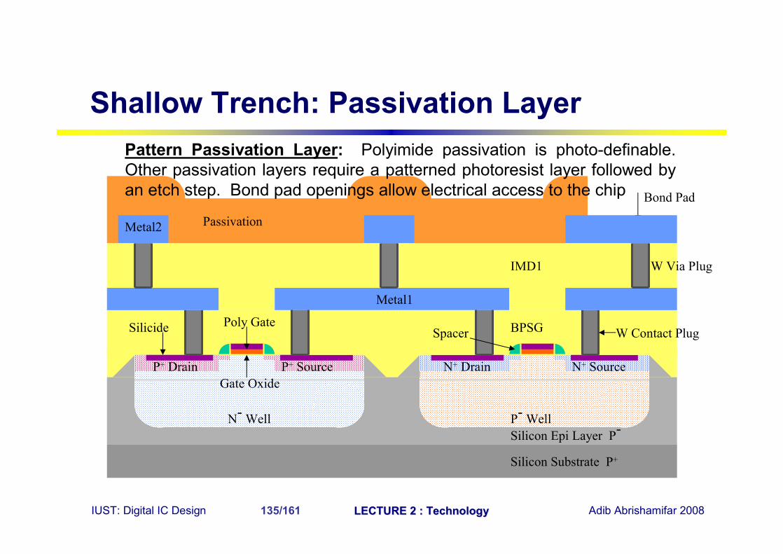
Passivation
Bond Pad
Poly Gate
Gate Oxide
Silicide Spacer
Metal2
Shallow Trench: Passivation LayerPattern Passivation Layer: Polyimide passivation is photo-definable. Other passivation layers require a patterned photoresist layer followed by an etch step. Bond pad openings allow electrical access to the chip
IUST: Digital IC Design LECTURE 2 : TechnologyLECTURE 2 : Technology Adib Abrishamifar 2008136/161
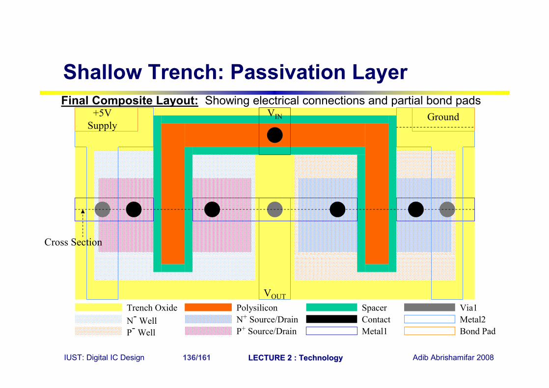
Cross Section
Final Composite Layout: Showing electrical connections and partial bond pads
Trench OxideN+ Source/DrainP+ Source/Drain
SpacerContactMetal1
Polysilicon Via1
+5V Supply
VOUT
N- WellP- Well
Metal2
Ground
Bond Pad
VIN
Shallow Trench: Passivation Layer
IUST: Digital IC Design LECTURE 2 : TechnologyLECTURE 2 : Technology Adib Abrishamifar 2008137/161
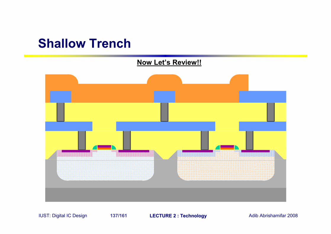
Now Let’s Review!!
Shallow Trench
IUST: Digital IC Design LECTURE 2 : TechnologyLECTURE 2 : Technology Adib Abrishamifar 2008138/161
MASK Generation Example CMOS Inverter
MASK
IUST: Digital IC Design LECTURE 2 : TechnologyLECTURE 2 : Technology Adib Abrishamifar 2008139/161
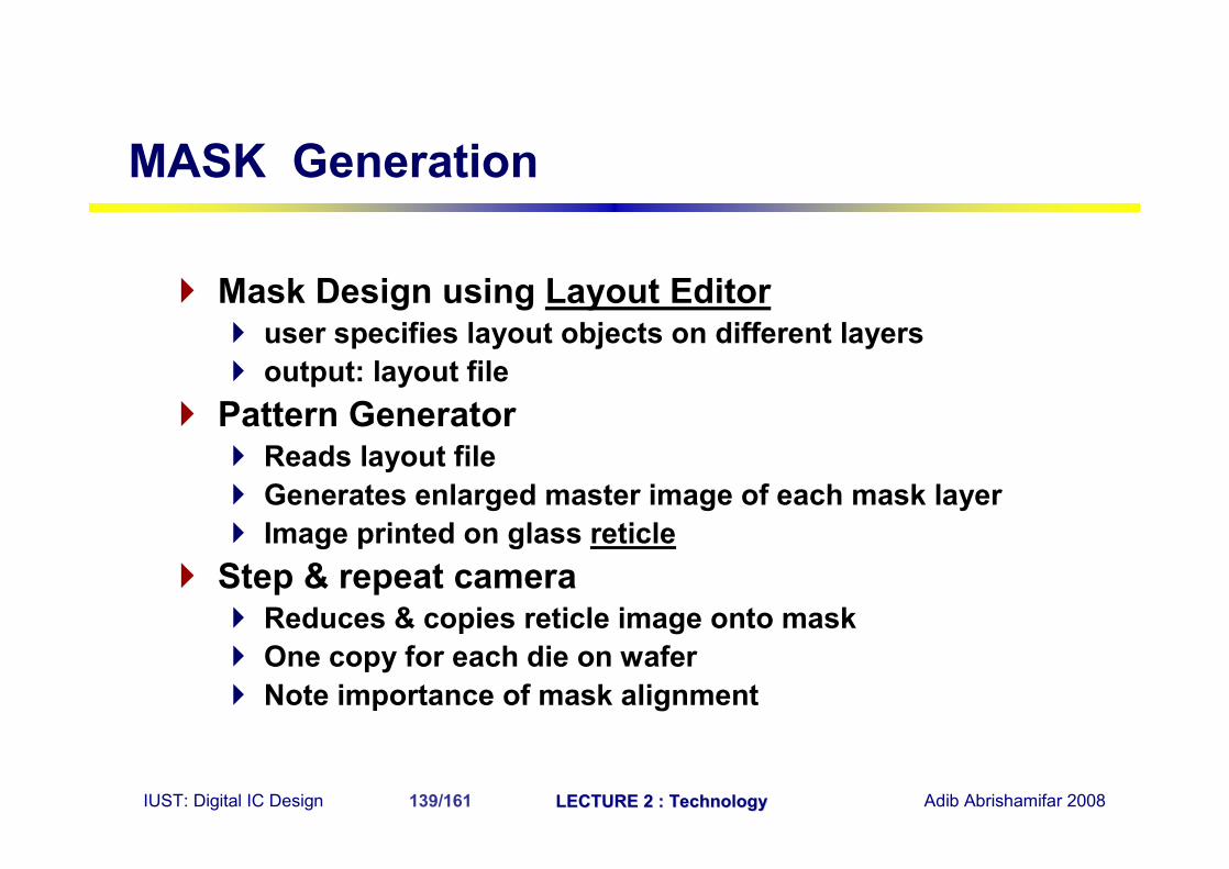
Mask Design using Layout Editor user specifies layout objects on different layers output: layout file
Pattern Generator Reads layout file Generates enlarged master image of each mask layer Image printed on glass reticle
Step & repeat camera Reduces & copies reticle image onto mask One copy for each die on wafer Note importance of mask alignment
MASK Generation
IUST: Digital IC Design LECTURE 2 : TechnologyLECTURE 2 : Technology Adib Abrishamifar 2008140/161
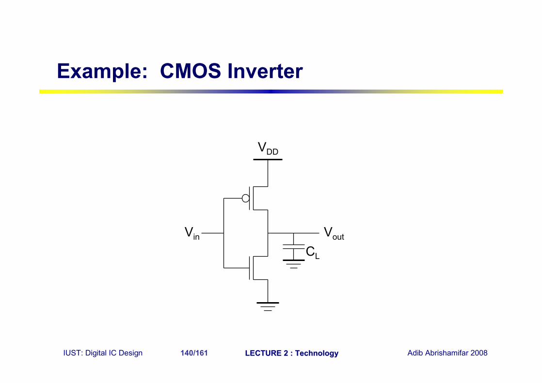
Example: CMOS Inverter
VDD
Vout
CL
Vin
IUST: Digital IC Design LECTURE 2 : TechnologyLECTURE 2 : Technology Adib Abrishamifar 2008141/161
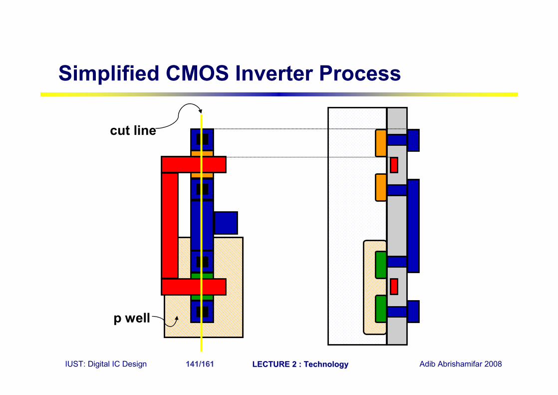
cut line
p well
Simplified CMOS Inverter Process
IUST: Digital IC Design LECTURE 2 : TechnologyLECTURE 2 : Technology Adib Abrishamifar 2008142/161
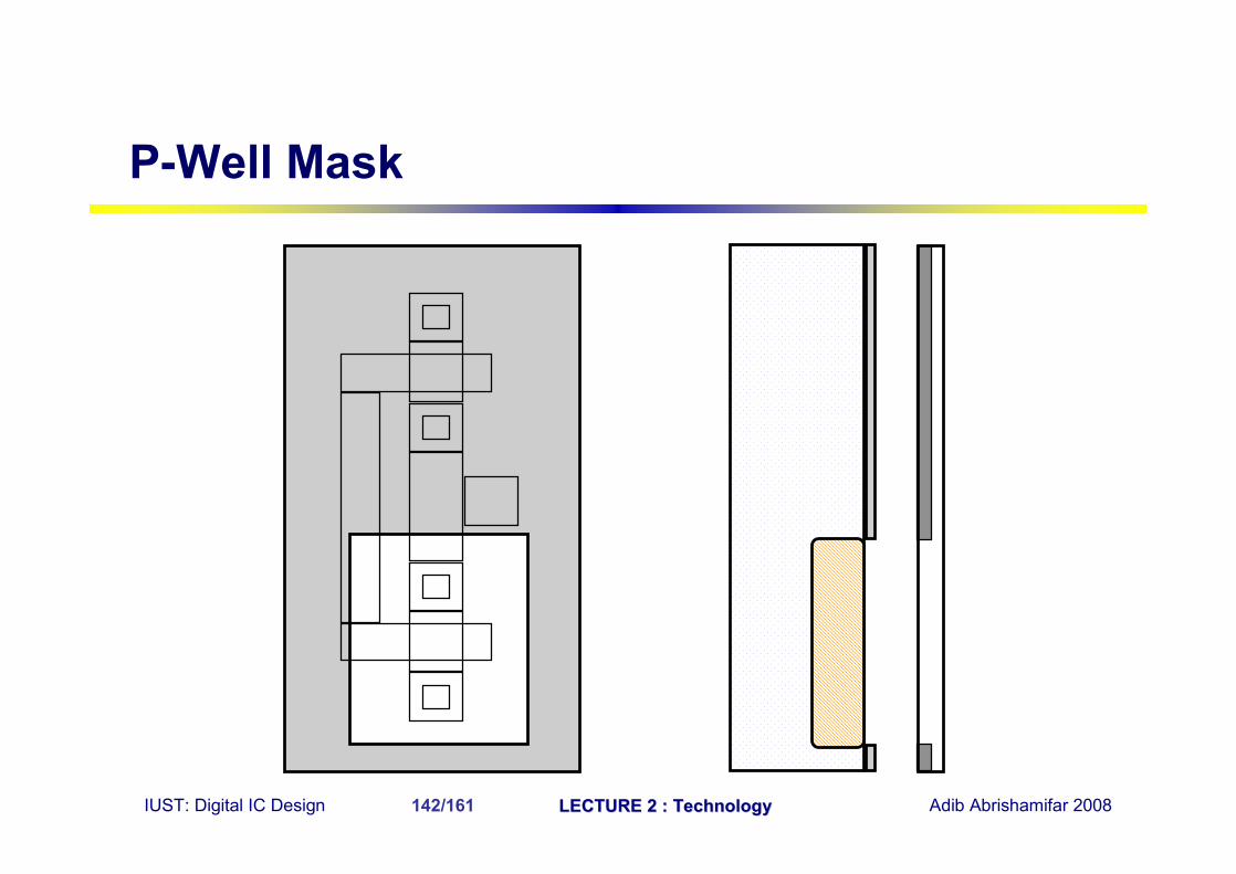
P-Well Mask
IUST: Digital IC Design LECTURE 2 : TechnologyLECTURE 2 : Technology Adib Abrishamifar 2008143/161
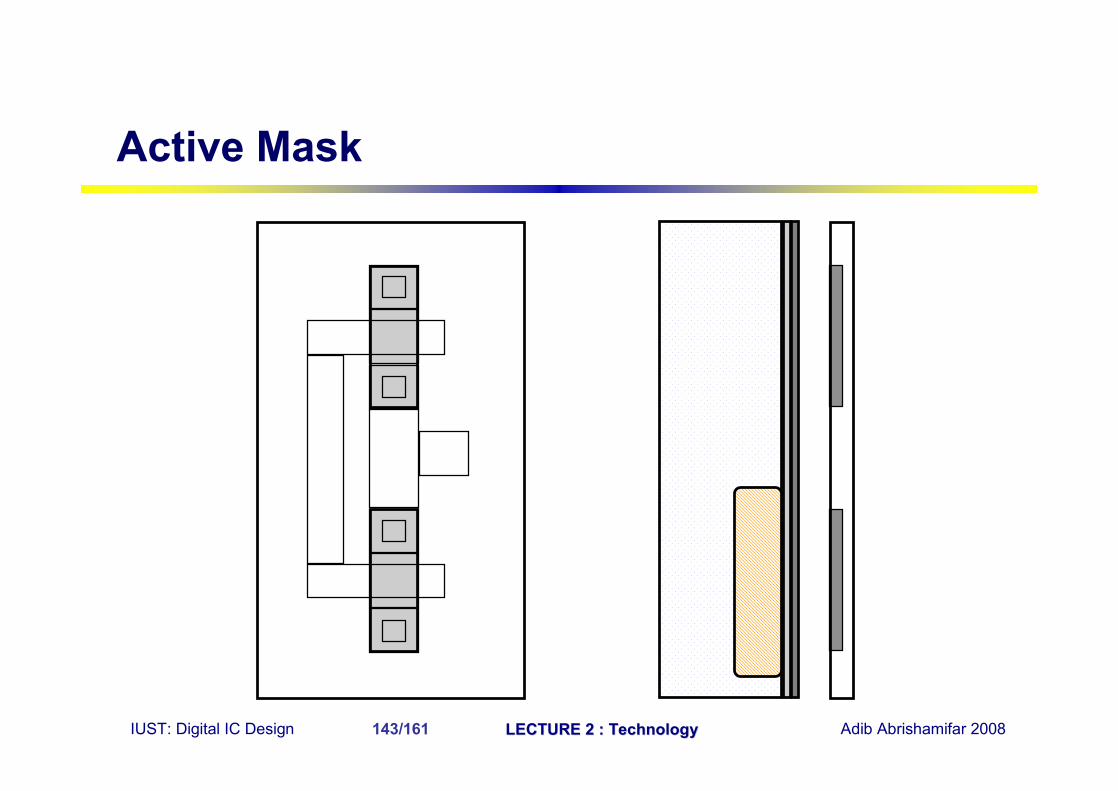
Active Mask
IUST: Digital IC Design LECTURE 2 : TechnologyLECTURE 2 : Technology Adib Abrishamifar 2008144/161
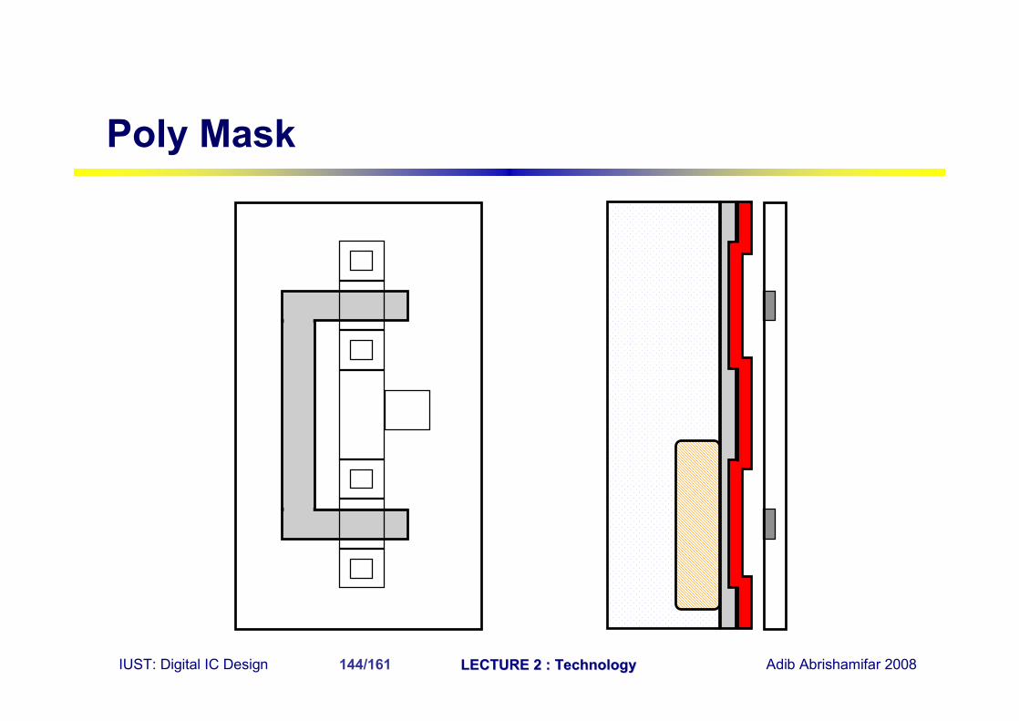
Poly Mask
IUST: Digital IC Design LECTURE 2 : TechnologyLECTURE 2 : Technology Adib Abrishamifar 2008145/161
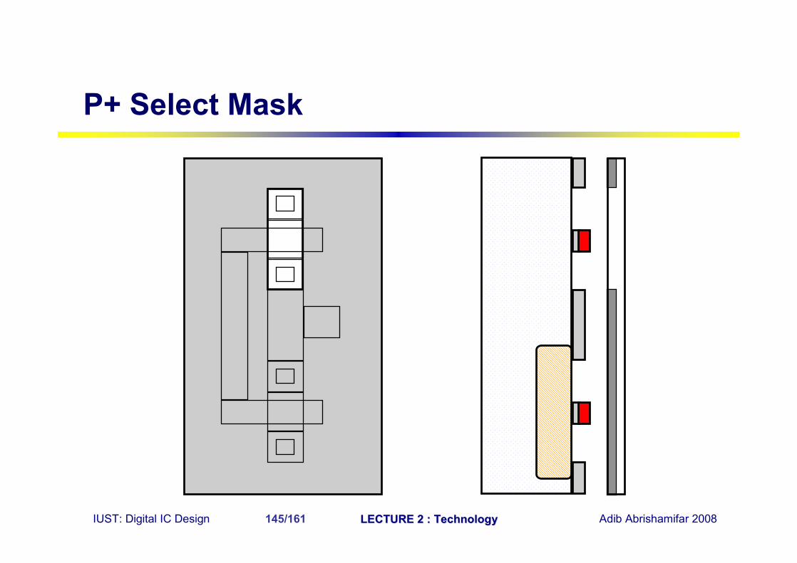
P+ Select Mask
IUST: Digital IC Design LECTURE 2 : TechnologyLECTURE 2 : Technology Adib Abrishamifar 2008146/161
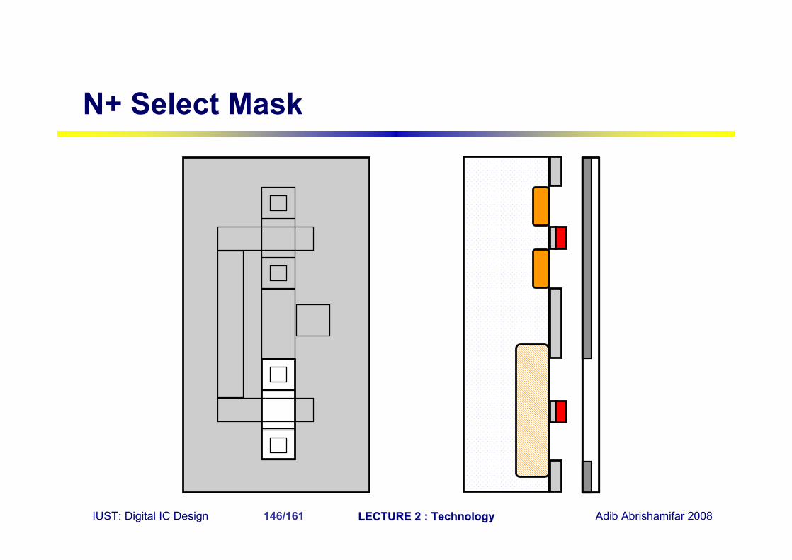
N+ Select Mask
IUST: Digital IC Design LECTURE 2 : TechnologyLECTURE 2 : Technology Adib Abrishamifar 2008147/161
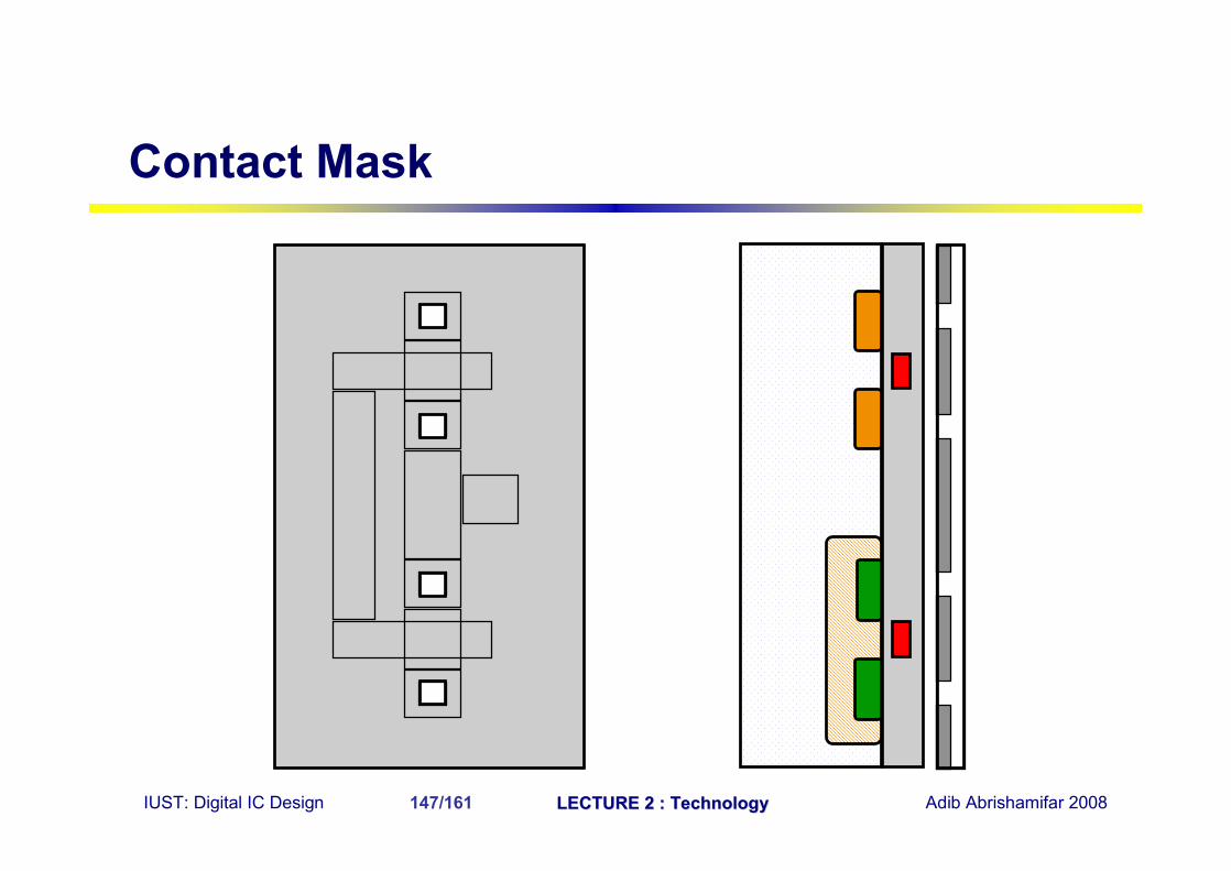
Contact Mask
IUST: Digital IC Design LECTURE 2 : TechnologyLECTURE 2 : Technology Adib Abrishamifar 2008148/161
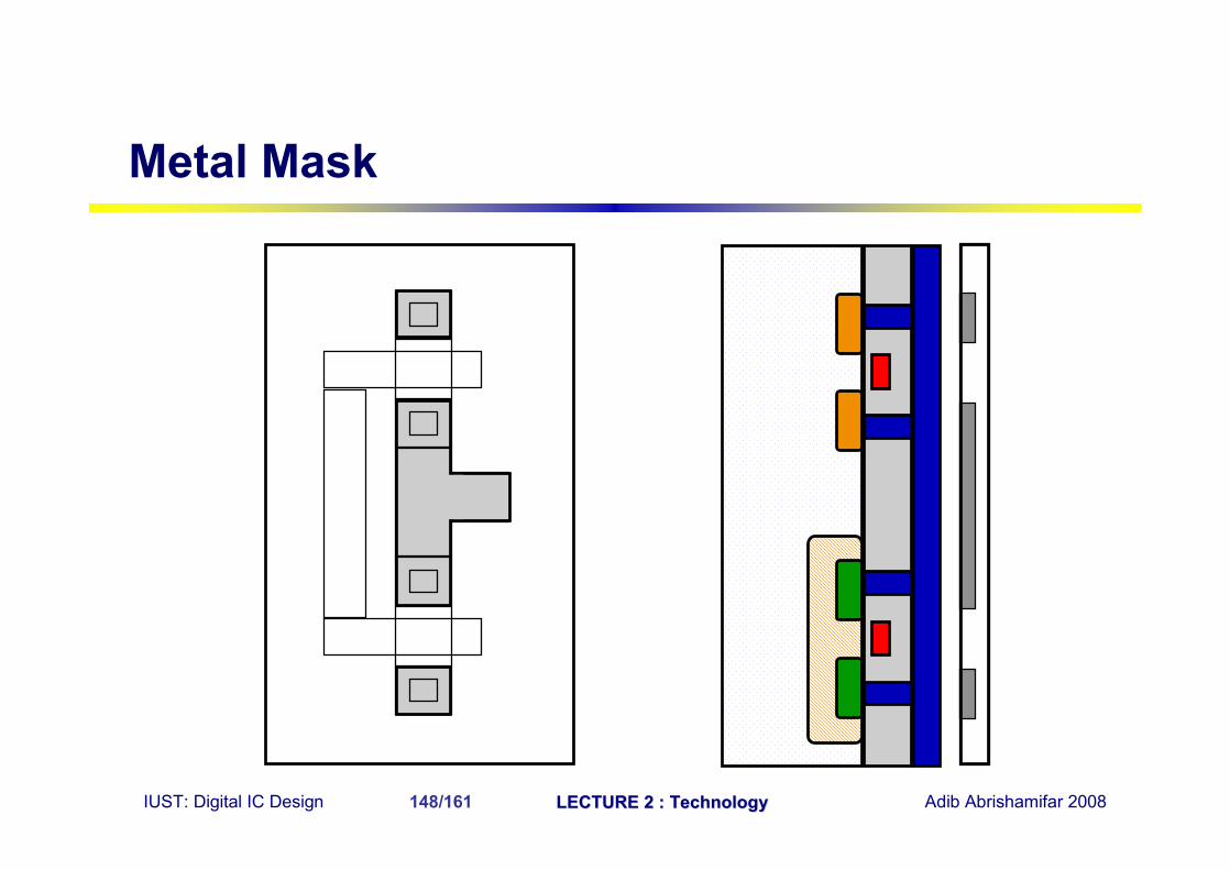
Metal Mask
IUST: Digital IC Design LECTURE 2 : TechnologyLECTURE 2 : Technology Adib Abrishamifar 2008149/161
Dual-Well CMOS + NPN Process Twin-Well Process + High energy Implantation Advanced Smart Power
Only one is described here
BiCMOS Processes
IUST: Digital IC Design LECTURE 2 : TechnologyLECTURE 2 : Technology Adib Abrishamifar 2008150/161
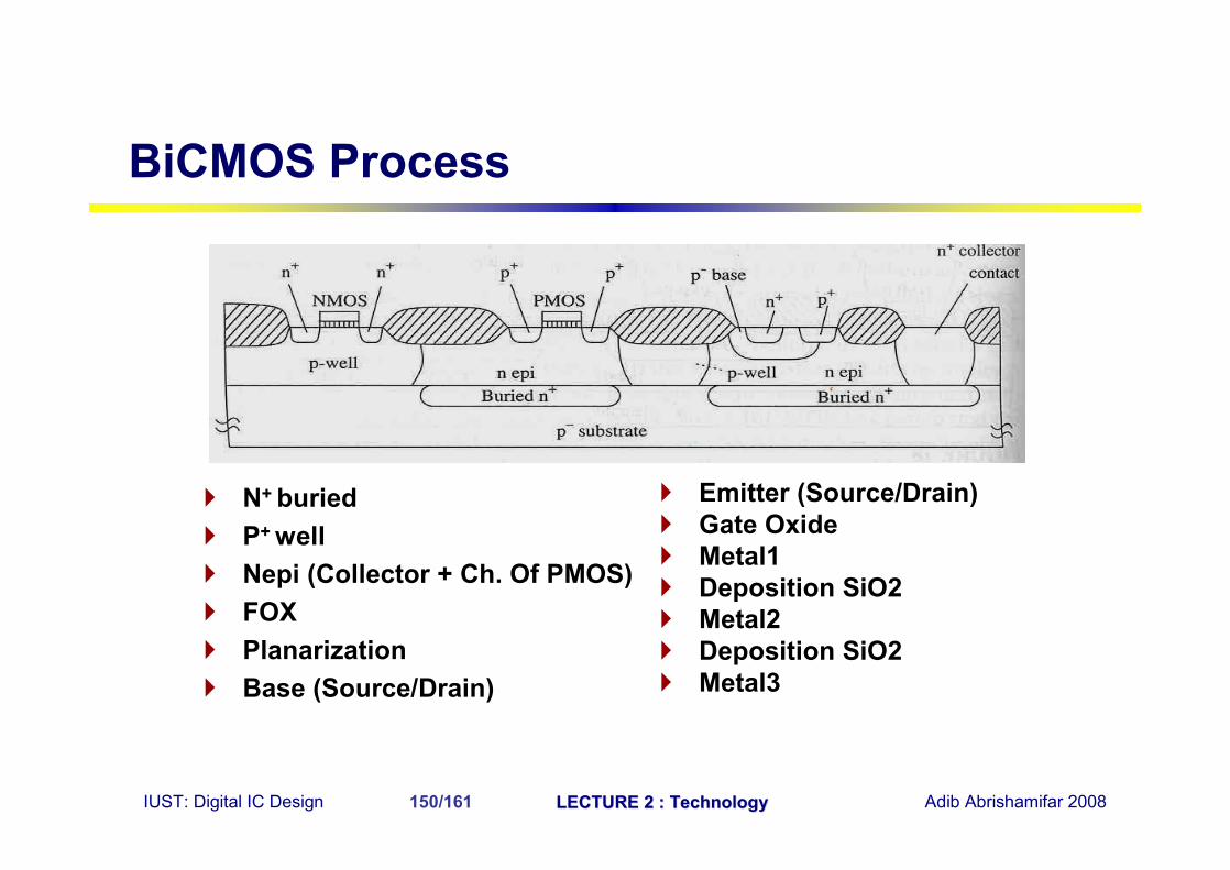
BiCMOS Process
N+ buried P+ well Nepi (Collector + Ch. Of PMOS) FOX Planarization Base (Source/Drain)
Emitter (Source/Drain) Gate Oxide Metal1 Deposition SiO2 Metal2 Deposition SiO2 Metal3
IUST: Digital IC Design LECTURE 2 : TechnologyLECTURE 2 : Technology Adib Abrishamifar 2008151/161
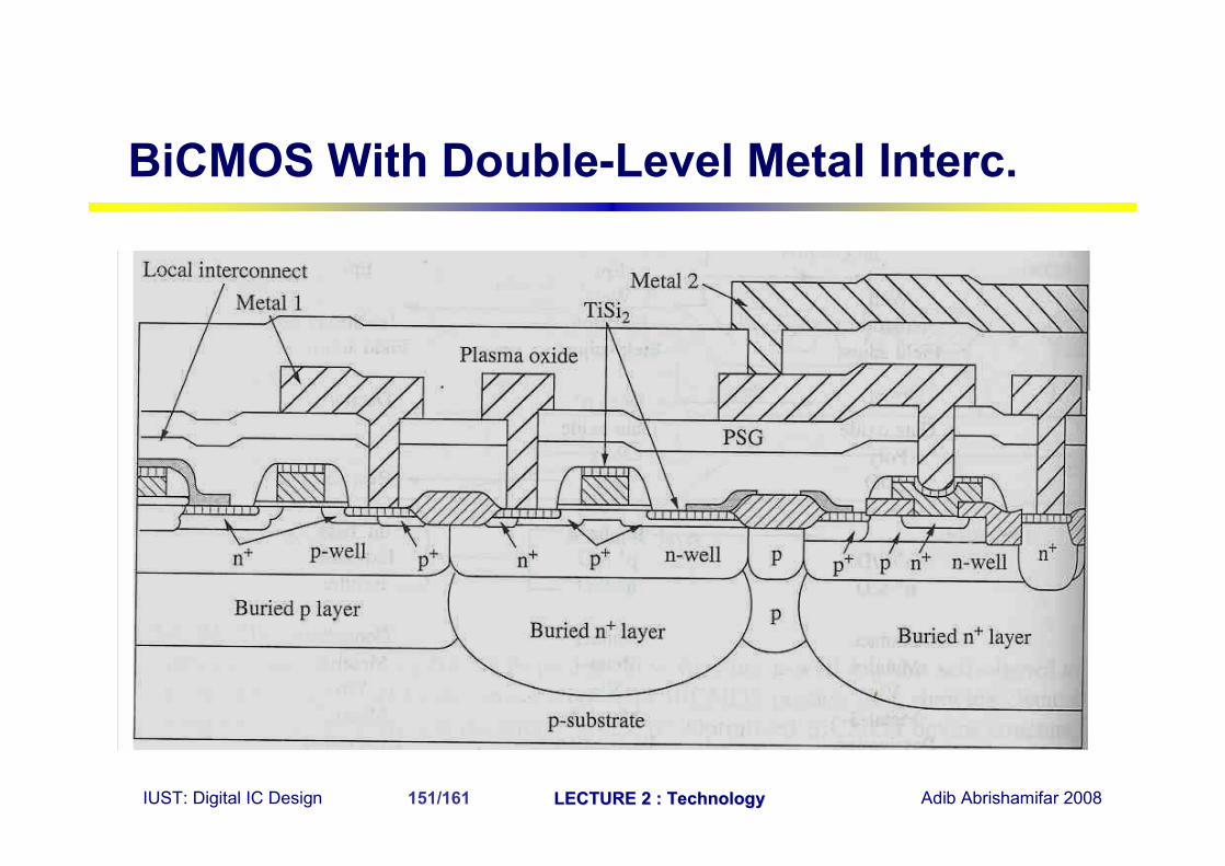
BiCMOS With Double-Level Metal Interc.
IUST: Digital IC Design LECTURE 2 : TechnologyLECTURE 2 : Technology Adib Abrishamifar 2008152/161
Why? Simple SOI CMOS Process SOI Wafer Fabrication (Basic Steps) SOI Transistors Disturbance Is SOI just in the textbooks? Novel SOI Devices
Silicon On Insulator (SOI)
IUST: Digital IC Design LECTURE 2 : TechnologyLECTURE 2 : Technology Adib Abrishamifar 2008153/161
Silicon on Insulator (SOI) is a new technology that has a number of advantages over ordinary silicon technologies including: SOI Devices are 25%-30% faster Replacement for SOS Need to extend Moore’s Law Commercial Availability of SOI wafers SOI Devices have less leakage current through the substrate
due to the buried insulator layer SOI Devices have reduced parasitic capacitance Improve Latch-up Susceptibility (Suitable for Sub-Micron) Higher Integration Density (Denser Layout = Low Cost)
Why SOI?
IUST: Digital IC Design LECTURE 2 : TechnologyLECTURE 2 : Technology Adib Abrishamifar 2008154/161
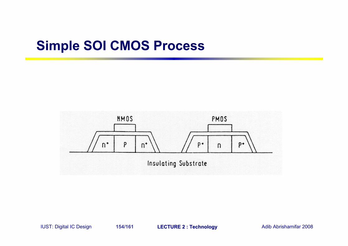
Simple SOI CMOS Process
IUST: Digital IC Design LECTURE 2 : TechnologyLECTURE 2 : Technology Adib Abrishamifar 2008155/161
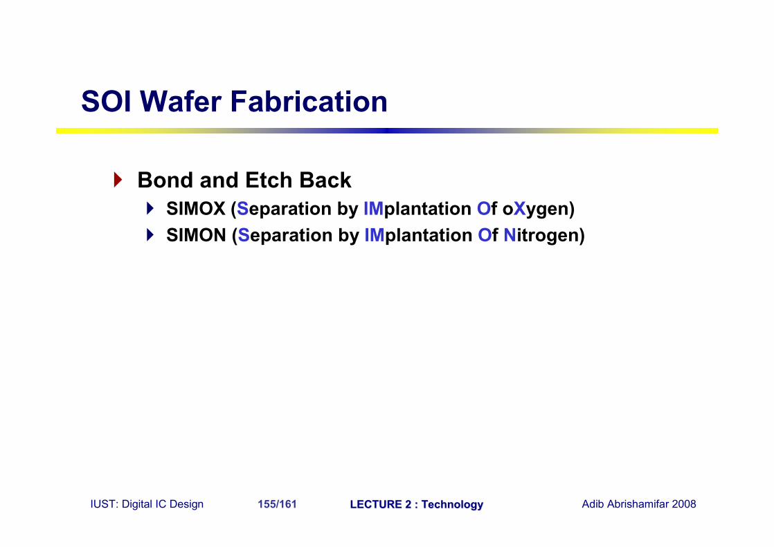
SOI Wafer Fabrication
Bond and Etch Back SIMOX (Separation by IMplantation Of oXygen) SIMON (Separation by IMplantation Of Nitrogen)
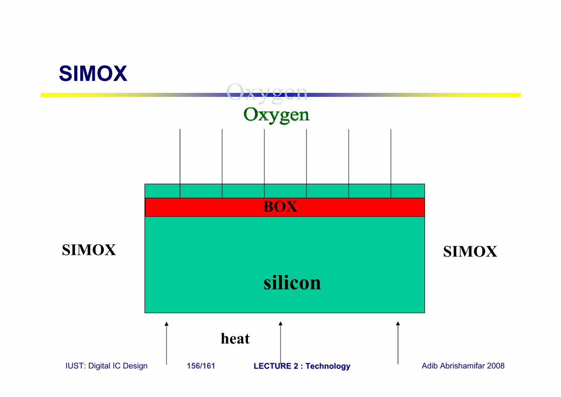
IUST: Digital IC Design LECTURE 2 : TechnologyLECTURE 2 : Technology Adib Abrishamifar 2008156/161
heat
silicon
BOX
SIMOX SIMOX
SIMOX
IUST: Digital IC Design LECTURE 2 : TechnologyLECTURE 2 : Technology Adib Abrishamifar 2008157/161
S il ic o n
S i l i c o n D io x id e 4 0 0 0 Å
S i l i c o n 9 0 0 Å
Source D rainSubstrate (G ate)
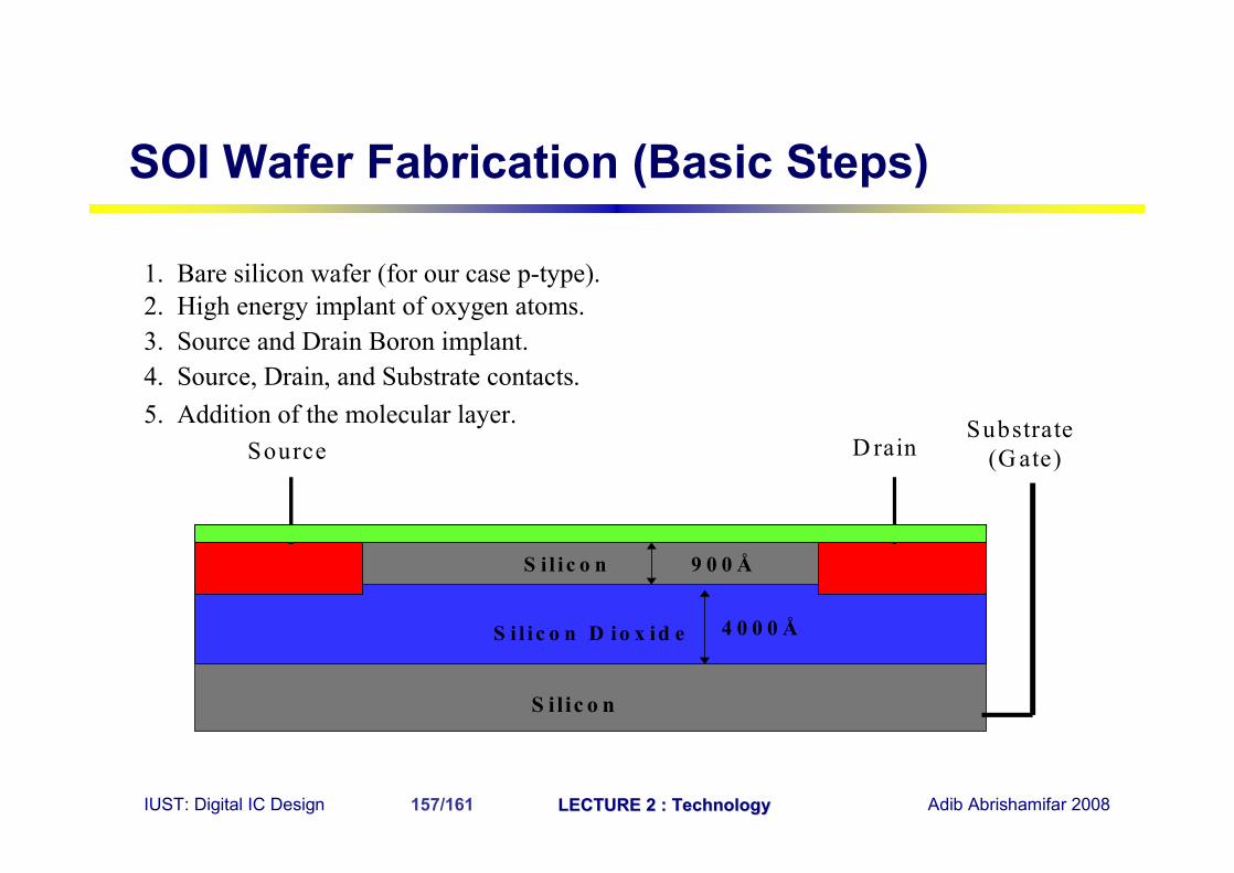
1. Bare silicon wafer (for our case p-type).2. High energy implant of oxygen atoms.3. Source and Drain Boron implant.4. Source, Drain, and Substrate contacts.5. Addition of the molecular layer.
SOI Wafer Fabrication (Basic Steps)
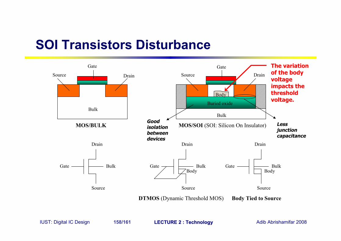
IUST: Digital IC Design LECTURE 2 : TechnologyLECTURE 2 : Technology Adib Abrishamifar 2008158/161
Bulk
DrainSource
Gate
MOS/BULK
Gate
Drain
Source
Bulk
DTMOS (Dynamic Threshold MOS) Body Tied to Source
Gate
Drain
Source
BulkBody
Gate
Drain
Source
BulkBody
Bulk
DrainSourceGate
Buried oxide
MOS/SOI (SOI: Silicon On Insulator)
Body
Less junction capacitance
Good isolation between devices
The variation of the body voltage impacts the threshold voltage.
SOI Transistors Disturbance
IUST: Digital IC Design LECTURE 2 : TechnologyLECTURE 2 : Technology Adib Abrishamifar 2008159/161
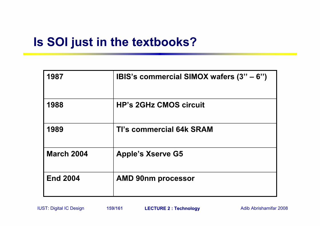
AMD 90nm processorEnd 2004
Apple’s Xserve G5March 2004
TI’s commercial 64k SRAM1989
HP’s 2GHz CMOS circuit1988
IBIS’s commercial SIMOX wafers (3’’ – 6’’)1987
Is SOI just in the textbooks?
IUST: Digital IC Design LECTURE 2 : TechnologyLECTURE 2 : Technology Adib Abrishamifar 2008160/161
Dual gate SOI SOI Single electron transistors
Novel SOI Devices
IUST: Digital IC Design LECTURE 2 : TechnologyLECTURE 2 : Technology Adib Abrishamifar 2008161/161
Future devices will involve SOI SOI provides certain benefits over bulk CMOS for
smaller gate lengths SOI SETs may become a promising technology in
the future
Summary