Embed Size (px)
Citation preview
Z. Salam et al./Journal of Energy & Environment, Vol. 5, May 2006 57
Digital Implementation of a New PWM Switching Scheme for Modular Structured Multilevel Voltage Source Inverter
Z. Salam*, J. Aziz** and S. S. Ahmed***
*Universiti Teknologi Malaysia, Johor Bahru, Malaysia **The University of Nottingham, United Kingdom
***Bangladesh University of Engineering and Technology, Dhaka, Bangladesh. Email: [email protected]
(Received on 15 Jan 2005, revised on 23 Jul 2005) ______________________________________________________________________________________
Abstract This work proposes a new switching scheme for the cascaded multilevel inverter that can be suitably implemented using digital technique. Unlike other schemes, the proposed method is based on the symmetric regular sampling unipolar PWM with a single carrier and multiple modulating signals. Non-transcendental trigonometric equations that define the switching instants of the multilevel inverter are derived. This algorithm is implemented using a low-cost fixed-point micro controller on an experimental five-level cascaded inverter test-rig. ______________________________________________________________________________________ Nomenclature MVSI Multilevel Voltage Source Inverter MSMI Modular Structured Multilevel Inverter N number of output voltage levels (N) of the cascaded inverter M number of H-bridge module (M) fo frequency of the output of the cascaded inverter f c switching frequency or carrier frequency Am amplitude of the modulation signal mf modulation frequency ratio mi modulation index Introduction In recent years, the electrical and machinery industries have begun to demand for power conversion equipment in the range of several Megawatts to be connected to a medium voltage network (2.3-6.9kV). Typical applications are the electric train, heavy-duty ac drives, conveyer belts, and unified power-flow controllers. However, power (semiconductor) switches with the suitable switching frequency at ratings above 5kV are rare; hence it is difficult to achieve inverter output voltage which is compatible to the medium voltage grid [1]. One approach is to utilise the multilevel voltage source inverter (MVSI) structure. Multilevel inverter is an array of power semiconductor switches and capacitor voltage sources, which is switched in a manner that an output voltage of stepped waveform is generated. For the normal two-level voltage source inverter, the maximum voltage output level is determined by the voltage blocking capability of each power switch. In contrast, for MVSI, the stress on each switch can be reduced in proportional to the number of output voltage levels. Thus with MVSI, higher input DC link voltage can be utilised using lower rated power switches.

Z. Salam et al./Journal of Energy & Environment, Vol. 5, May 2006 58
Besides this important point, there are other advantages of the MVSI. It is possible to remove the expensive and bulky step-up transformer for applications that does not require galvanic isolation. Furthermore MVSI is known to improve harmonics performance, resulting in reduced switching losses. This is particularly crucial for high power application as increased power losses can complicate thermal management system design. With several levels in output waveform constructed using MVSI, the dV/dt on each power switch is reduced and so thus the EMI problem. MVSI topologies The development of MVSI began in the early 1980’s when Nabae et al. [2] proposed the neutral-point clamped (NPC) pulse width modulation (PWM) inverter. Since then several multilevel topologies have evolved; most common are the NPC or Diode-Clamped Multilevel Inverter [2-4], Flying-Capacitor Multilevel Inverter [5] and Modular Structured Multilevel Inverter [6]. In addition there are emerging multilevel topologies such as the asymmetric hybrid cells [7] and soft-switching multilevel inverters [8]. A brief description of the three main MVSI topologies is given below. Diode-Clamped Multilevel Inverter (DCMI) The DCMI uses capacitors in series to divide up the dc bus voltage into a set of voltage levels. An example of a single-phase four-level DCMI and its output voltage waveform is shown in Figs.1 and 2. To produce N-levels of the phase voltage, the DCMI requires N-1 capacitors on the dc bus. Thus for a four-level inverter, the dc bus consists of three capacitors C1, C2 and C3. For a dc bus voltage of Vdc, the voltage across each capacitor is Vdc/3. Consequently the voltage stress for each power device is limited to Vdc/3, through the clamping diodes.
Sa3
Sa'1
Sa'2
S a'3
S b1
Sb2
Sb3
S b'1
Sb'2
S b'3
Load
Sa1
Vdc a
b
o
C1
C2
C3
Sa2
leg a leg b
Fig. 1 A single phase four level DCMI

Z. Salam et al./Journal of Energy & Environment, Vol. 5, May 2006 59
V4
V3
V2
V1
-V4
-V3
-V2
Vao
Vob
t
Fig. 2 Output voltage waveform
Although each power switch only required to block a voltage level of Vdc/3, each clamping diodes need to have different voltage ratings for reverse voltage blocking. Assuming that each blocking diode voltage rating is the same as the power switches, the relationship between the diodes and the output voltage levels is expressed as (N-1)×(N-2)]. This represents a quadratic increase with respect to N, and for high level inverters, the system impractical to implement. Furthermore, the voltage unbalance problem across the capacitor make this topology is unattractive to handle real power flow control. Flying-capacitor multilevel inverter (FCMI) Fig. 3 illustrates the fundamental building block of a single-phase four-level FCMI. The voltage level defined is similar to that of the DCMI. To generate N-level staircase output voltage, N-1 capacitors on the dc bus are needed. It is obvious that two inner-loop balancing capacitors for phase leg a, Ca1 and Ca2 are independent from those for phase leg b. Both phase leg share the same dc link capacitors, C1, C2 and C3. The advantage of this topology is that it eliminates the clamping diode problems present in the DCMI. In addition, the large amount of capacitance provide extra ride through capabilities during power outage. Similar to DCMI, the harmonic content is proportional with the level of the inverter, thus it’s possible to avoid the output filters. Furthermore, this topology naturally limits the dV/dt stress across the devices and introduces additional switching states that can be used to maintain the charge balance in the capacitors. However, FCMI has several technical difficulties that complicate its practical application for-high power converters. To maintain the charge balance in the capacitors, the dc-link capacitors need a controller, thus adding complexity to the control of the overall circuit. Furthermore, an excessive number of storage capacitors are required when the number of inverter level is high. Therefore it is more difficult to package the bulky capacitors.

Z. Salam et al./Journal of Energy & Environment, Vol. 5, May 2006 60
S a1
S a2
S a3
S a'3
S a'2
S a'1
S b1
S b2
S b3
S b'3
S b'2
S b'1
C a2
C a2
C a1
C 1
C2
C3
Cb2
C b2
C b1 b
Load
a
Vdc
o
leg a leg b
Fig. 3 Circuit of a single phase four level FCMI
Modular structured multilevel inverters (MSMI) The MSMI, shown in Fig. 4, utilises separate dc sources to construct the multilevel phase voltage by means of H-bridges inverter modules. Due to its modular structure, it is also known as the cascaded MVSI. It inherits several advantages over other multilevel topologies in terms of circuit modularity, protection and packaging. In addition the cascaded structure requires the least number of components among all multilevel topologies to achieve the same output voltage levels. Furthermore it does not suffer the voltage-balancing problem as experienced by the DCMI. The MSMI inverter is well suited for renewable energy applications because naturally, renewable energy sources provide separate dc sources. This topology will be discussed in more details in the following sections.

Z. Salam et al./Journal of Energy & Environment, Vol. 5, May 2006 61
E 1
E 2
E M
S 11 S 21
S 31 S 41
S 12 S 22
S 32 S 42
S 1M S 2M
S 3M S 4M
Module 1
Module 2
Module M
V1
V2
VM
Vphase( V out )
0
+–
+_
+_
Fig. 4 Structure of a MSMI MVSI modulation techniques In general, the modulation control of MVSI is more complicated than the two-level VSI due to the need to cater for the transitions between the voltage levels (or steps). This was demonstrated by previous works, for example [5, 9-12]. Efforts form these researchers have established the sinusoidal natural sampling PWM (SPWM) as the most popular modulation method. Other modulation methods such as the space vector PWM modulation (SVPWM) [13] and harmonics elimination PWM (HEPWM) [14-15] has also been applied to multilevel topologies for specific applications. The SPWM for MVSI is based on the intersection of a single sinusoidal reference with N-1 triangular carrier signals. The resulting intersection points become the switching instants of the PWM pulses. As far as the carrier signals alignment is concerned, three carrier phase shifting (or commonly known as the disposition method) schemes are suggested:
• Phase disposition (PD) where all the carrier signals are in phase, • Alternative phase opposition disposition (APOD) where the carrier signals above the zero line of
sinusoidal modulating waveform are 180 out of phase with those below the zero line, and • Phase disposition (POD), where each carrier signal is phase shifted by 180 from its adjacent
carriers.
Figs. 5(a) to 5(c) show these disposition techniques. Each of these variations has particular harmonic benefits, which have been argued extensively in [11].

Z. Salam et al./Journal of Energy & Environment, Vol. 5, May 2006 62
(a) APOD
(b) POD
(c) PD
Fig. 5 Phase disposition of the five level MVS While the literature on the modulation techniques for MVSI can be considered extensive, there seems to be inadequate description on how such scheme can be implemented effectively on a digital system. For the multi carrier schemes described in [16], digital implementation results in an inherent “jump” in more than one level of the output voltage during level transitions. The level jumps seriously distort the output voltage waveform, thus degrading its harmonics spectra. The same authors proposed software solutions to check and then to avoid these undesired conditions. However the correction scheme is rather complicated and its practical implementation can be quite cumbersome. This work attempts to propose an alternative switching scheme for the MSMI that utilizes the symmetric regular sampling unipolar PWM. Unlike other schemes, the proposed method is based on the intersection of a single carrier waveform with multiple modulating signals. It was discovered that by using this technique, switching transitions can be programmed effectively using a simple fixed-point microprocessor. It was also observed that the level jumping problem vanished. To the benefit of the readers, the paper begins by outlining the principle of the modulation and the derivation trigonometric equations that define the switching instant. To determine the effectiveness of the algorithm, a Matlab-Simulink simulation is carried out. Finally, to validate workability of the proposed scheme, a single-phase five-level MSMI is built and tested.
The proposed Modulation Scheme Modulation principle The proposed scheme is implemented on a MSMI. For convenience, an N-level, single-phase MSMI is redrawn as Fig 6. The ac output voltage of each module is connected in series to form an output voltage, Vout. The number of H-bridge module (M), depends on the number of levels (N) required and can be written as:

Z. Salam et al./Journal of Energy & Environment, Vol. 5, May 2006 63
N 1M=
2−
(1)
It is usually assumed that N is odd, as this would give an integer-valued M. By different combinations of the four switches, S1M through S4M, each module can generate three different voltage outputs, i.e. +E, E, and 0. The total output voltage is then constructed by the sum of the output voltage from each module. For example, a five level inverter would have an output levels of +2E, +E, 0, E, and –2E.
E 1
E 2
E M
S 11 S 21
S 31 S 41
S 12 S 22
S 32 S 42
S 1M S 2M
S 3M S 4M
Module 1
Module 2
Module M
V1
V2
VM
Vphase(V out )
0
+–
+_
+_
Fig. 6 MSMI Structure
The proposed modulation scheme is based on the classical unipolar, symmetric PWM switching technique. The method compares several modified sinusoidal modulation signals su(k) with a single triangular carrier signal c(k) as shown in Fig. 7. Each of these modified modulation signals have the same frequency (fo) and amplitude (Am). The carrier signal is a train of triangular waveform with frequency fc and amplitude Ac. Equations (2) and (3) define the modulation index and ratio for N-level inverter with M number of modules:
1(N 1) M
2
m mi
c c
A Am
A A= ⋅ =
− (2)
c of f fm = (3)
The variable k represents a position of each modulated width pulses, initiated from k= 1,2,3…mf/2. Intersection between the modified modulation signals and the carrier signal defines the switching instant of the PWM pulses.

Z. Salam et al./Journal of Energy & Environment, Vol. 5, May 2006 64
Fig. 7 The modified sinusoidal modulation signals with a single carrier signal. Waveform labels: (a) Carrier signal c(k), (b) Absolute sinusoidal modulation signal m1 (t), (c) Modified sinusoidal modulation
signal s1(k) of m1 (t), (d) Shifted absolute sinusoidal modulation signal m2 (t), (e) Modified sinusoidal modulation signal s2(k) of m2 (t).
To illustrate the principle of the proposed scheme, a five-level inverter at mi = 0.4 and mi=0.8 for E=100V is shown in Figs 8 and 9, respectively. For clarity, a low value of mf, i.e 20 is arbitrary chosen. For a five level output, two modulation signals namely s1(k) and s2(k) and single triangular carrier c(k) are involved in the modulation process. Signal s2(k) is actually s1(k) that shifted down by the amplitude of triangular carrier signals Ac. In general signal su+1(k) is shifted down by Ac from su(k). The PWM pulses V1(k) is generated from the comparison between s1(k) and c(k), while V2(k) is from comparison between s2(k) and c(k). The comparison is designed such that if s1(k) is greater than c(k), a pulse-width V1(k) is generated; if s2(k) is greater than c(k), V2(k) is generated. On the other hand if there is no intersection, then V1(k) and V2(k) remain at 0. It can be seen in Fig. 6 that for the case of mi≤ 0.5, only s1(k) and carrier signal c(k) is involved in the modulation process. There is no intersection for s2(k). Therefore, the output pulse V2(k) is zero. The output voltage Vout, which is the sum of V1(k) and V2(k), is then similar to the conventional three-level unipolar PWM case. For mi>0.5, as depicted in Fig. 7, both modulating signal, i.e. s1(k) and s2(k) intersect the carrier and therefore V1 and V2 pulses are generated. As a result, a multilevel output voltage Vout is formed.

Z. Salam et al./Journal of Energy & Environment, Vol. 5, May 2006 65
Fig. 8 Proposed modulation scheme for mi = 0.4, mf = 20.Traces: (a) Modulation signals and carrier signal (b) PWM pulses produced from comparison between s1(k) and c(k), V1(k); (c) PWM pulses produced from
comparison between s2(k) and c(k), V2(k); (d) PWM output waveform
Fig. 9 Proposed modulation scheme for mi = 0.8, mf = 20. Traces: (a) Modulation signals and carrier signal; (b) PWM pulses produced from comparison between s1(k) and c(k), V1(k); (c) PWM pulses produced from
comparison between s2(k) and c(k), V2(k); (d) PWM output waveform.
Z. Salam et al./Journal of Energy & Environment, Vol. 5, May 2006 66
For a N-level inverter there are M modulating waveform, which corresponds to M number of H-bridge modules. The nth level transitions occur at:
= ; 1... -1Minm n M= (4)
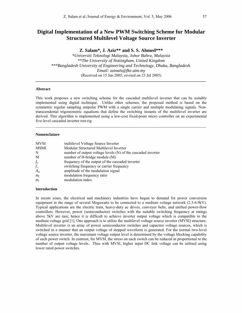
For example for a 9 level inverter, N=9; therefore M=4. The transition occurs when the modulation index mi reaches 0.25, 0.5 and 0.75. Note that the definition of modulation index used in this discussion is given by Equation (2). Derivation of the switching angle equations It can be seen that the kth rising edge is defined as the intersection of the negative slope carrier c¯(k) and two set of modulating signals s1(k) and s2(k). Since the waveform is symmetrical, the intersection of the positive slope carrier c+(k) and the modulating signals is not required. It can be deduced from the rising edge equations, i.e. the intersection between c¯(k) and s1 (k) or s2 (k) as shown in Fig. 10.
Fig. 10 Intersection between single carrier and modified sinusoidal modulation signals
The straight-line equation for the carrier wave is denoted by c¯(k) for the negative slope. It can be expressed as:
( ) ; 1,2,3....; 1,3,5....
2
ck c
c
Ac k hA k h
Tα−
⎛ ⎞⎜ ⎟−
= + = =⎜ ⎟⎜ ⎟⎜ ⎟⎝ ⎠
(5)
Z. Salam et al./Journal of Energy & Environment, Vol. 5, May 2006 67
Where fc is a carrier frequency and fo is a modulating signal frequency. The symmetric regular sampled modulation signals s1(k) and s2(k) can be expressed as:
1 2( ) sin ( ) and ( ) sin ( )m mf f
s k A i s k A im mπ πω ω
⎡ ⎤ ⎡ ⎤= + = +⎢ ⎥ ⎢ ⎥
⎢ ⎥ ⎢ ⎥⎣ ⎦ ⎣ ⎦cA− (6)
Where 0,1, 2... -1 2
fmi = when s1(k) and s2(k) intersects with c¯(k). The angular frequency ω , in (6) is
represented by 2 fmπ . Using the arithmetic regression and the kth raising edge ( 1( )kα ) of PWM signal V1 (k) is produced by the intersection between s1 (k) and c¯(k), i.e.:
1 ( ) sin ( ) ; 2 1 and 1
2
cc m
c f
Ak hA A i h k i k
T mπα ω
⎛ ⎞⎜ ⎟ ⎛ ⎞−
+ = + = − = −⎜ ⎟⎜ ⎟ ⎜ ⎟⎜ ⎟ ⎝ ⎠⎜ ⎟⎝ ⎠
(7)
Solving, this rising edge kth transition point 1( )kα is represented by:
( )1( ) 2 1 sin ( 1)2c m
c f
T Ak k k
Aπα ω
⎡ ⎤⎛ ⎞= − − − +⎢ ⎜⎜⎢ ⎥⎝ ⎠⎣ ⎦m
⎥⎟⎟ (8)
Using the same method, i.e. the intersection between s2(k) with c¯(k), every rising edge 2 ( )kα of PWM signal V2(k) can be expressed as:
2 ( ) 2 sin ( 1)2c m
c f
T Ak k k
Aπα ω
⎡ ⎤⎛ ⎞= − − +⎢ ⎜⎜⎢ ⎥⎝ ⎠⎣ ⎦m
⎥⎟⎟ (9)
Equations (8) and (9) can be generalized to produce a general switching angle for an N-level inverter:
( ) (2 2) sin ( 1)2c m
uc f
T Ak k u kA
πα ω⎡ ⎤⎛ ⎞
= + − − − +⎢ ⎜⎜⎢ ⎥⎝ ⎠⎣ ⎦m⎥⎟⎟ (10)
Where u=1,2..M and N 1M=
2−
. Equation (10) can be used to generate the kth PWM pulses for a cascaded
inverter of any level N. Note that the variable u corresponds to the particular H-bridge module that the switching will be subjected on. It follows that uα is the switching angle for the kth pulse of a particular bridge module. It can also be noted that this equation (10) is non-transcendental. All the variables at the

Z. Salam et al./Journal of Energy & Environment, Vol. 5, May 2006 68
right hand side of this equation are known and therefore the switching angles can be calculated directly. Its practical implementation using digital technique is therefore quite straightforward.
Simulation of a Five Level MSMI To obtain an insight on the proposed modulation scheme, a MATLAB-Simulink simulation of a five-level MSMI, shown in Fig. 11 is carried out. The DC source is set to 100V. The fundamental and switching frequency is set to 50HZ and 1Khz, respectively. This corresponds to mr of 20.
E
S11 S21
S31 S41
Module 1
Vphase(Vout)
E
S12 S22
S32 S42
Module 2
Fig. 11 Single phase five level MSMI.
Simulink block diagram to generate PWM signals V1(k) and V2(k) is shown in Fig. 12. To produce a five level inverter with mi greater than 0.5, two modulation signals are required namely, s1(k) and s2(k). Signal s1(k) is created after symmetric regular sampled passed through absolute block (Abs) while signal s2(k) is formed when s1(k) is subtracted with the amplitude of carrier signal. For simulation purpose, amplitude of carrier signal c(k) is set to 1 p.u.

Z. Salam et al./Journal of Energy & Environment, Vol. 5, May 2006 69
Fig. 12 Simulink block diagram for PWM signal generation
Each modulation signals s1(k) and s2(k) is separately compared to a single carrier signal c(k) using comparator 1 and 2. The output signals V1(k) and V2(k) obtained after this comparison are shown in Fig. 13. However it has to be noted that if mi less than 0.5, only V1(k) is generated while V2(k) is always zero as shown in Fig. 15(a). This is because the intersection occurred only between s1(k) and c(k), while for s2(k), it is not intersected at all.
(a)
(b)
Fig.13 Simulation result of PWM signals generation with (a) mi ≤ 0.5, (b) mi > 0.5 For a five-level MSMI, there are 16 different switches configurations for the gating signals. For this work, the selected switching state configuration is shown in Table 1. The selection is advantageous because only one pair of the power devices in each module needs to be switched at high frequency. Another pair is commutated at the fundamental frequency. In effect, the overall switching losses of the inverter are reduced.
Z. Salam et al./Journal of Energy & Environment, Vol. 5, May 2006 70
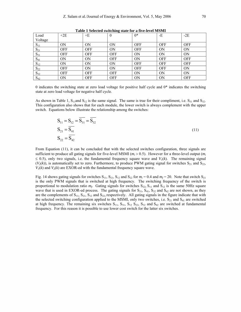
Table 1 Selected switching state for a five-level MSMI
Load Voltage
+2E +E 0 0* -E -2E
S11 ON ON ON OFF OFF OFF S21 OFF OFF ON OFF ON ON S31 OFF OFF OFF ON ON ON S41 ON ON OFF ON OFF OFF S12 ON ON ON OFF OFF OFF S22 OFF ON ON OFF OFF ON S32 OFF OFF OFF ON ON ON S42 ON OFF OFF ON ON OFF
0 indicates the switching state at zero load voltage for positive half cycle and 0* indicates the switching state at zero load voltage for negative half cycle.
As shown in Table 1, S11and S12 is the same signal. The same is true for their compliment, i.e. S31 and S32. This configuration also shows that for each module, the lower switch is always complement with the upper switch. Equations below illustrate the relationship among the switches:
11 12 31 32
21 41
22 42
S S S S
S S
S S
= = =
=
=
(11)
From Equation (11), it can be concluded that with the selected switches configuration, three signals are sufficient to produce all gating signals for five-level MSMI (mi > 0.5). However for a three-level output (mi ≤ 0.5), only two signals, i.e. the fundamental frequency square wave and V1(k). The remaining signal (V2(k)), is automatically set to zero. Furthermore, to produce PWM gating signal for switches S21 and S22, V1(k) and V2(k) are EXOR-ed with the fundamental frequency square wave. Fig. 14 shows gating signals for switches S11, S21, S12 and S22 for mi = 0.4 and mf = 20. Note that switch S21 is the only PWM signals that is switched at high frequency. The switching frequency of the switch is proportional to modulation ratio mf. Gating signals for switches S22, S11 and S12 is the same 50Hz square wave that is used in EXOR-ed process. The gating signals for S31, S41, S32 and S42 are not shown, as they are the complements of S11, S21, S12 and S22, respectively. All gating signals in the figure indicate that with the selected switching configuration applied to the MSMI, only two switches, i.e. S21 and S41 are switched at high frequency. The remaining six switches S11, S31, S12 S22, S32 and S42 are switched at fundamental frequency. For this reason it is possible to use lower cost switch for the latter six switches.

Z. Salam et al./Journal of Energy & Environment, Vol. 5, May 2006 71
Gating signal for S11 Gating signal for S21
Gating signal for S12 Gating signal for S22
Fig. 14 Gating signals of five-level MSMI with mi = 0.4 and mf = 20. Fig. 15 shows gating signals for mi = 0.8 and mf = 20. For this case, four switches S21, S41, S22 and S42 are switched at high frequency. The remaining four switches S11, S31 and their complements are switched at fundamental frequency.
Gating signal for S21 Gating signal for S21
Gating signal for S12 Gating signal for S22
Fig. 15 Gating signals of five-level MSMI with mi = 0.8 and mf = 20
To obtain the output voltage, all gating signals S11, S21, S31, S41, S12, S22, S32 and S42 are connected to their respective power switches. Fig. 16 shows the inverter output waveform for mi=0.4 and mi = 0.8, respectively.
(a)
(b)
Fig. 16 Output voltage waveform: (a) mi = 0.4 and mf = 20 (b) mi = 0.8 and mf = 20

Z. Salam et al./Journal of Energy & Environment, Vol. 5, May 2006 72
Hardware Implementation Generation of PWM waveform A five-level 250 Watts experimental rig is built to prove the effectiveness of the proposed modulation technique. The inverter input voltages are fixed at 100V dc for each H-bridge module with pure resistive load. The PWM signal generation is performed by the SIEMENS SAB-C167CR-LM fixed-point microcontroller. Integrated on-chip peripherals such as Serial Port, bi-directional Parallel Port, Timers, PWM module and Peripheral Interfaces units make the interfacing task much easier and with higher reliability. To obtain a five-level output voltage as described in the simulation section, three signals need to be generated, namely the fundamental frequency square wave, the PWM signal V1(k) and the PWM signal V2(k). These signals are generated using on chip PWM module. The PWM module eliminates the requirement for complicated external timers. It allows the generation of up to four independent PWM signals. The standard PWM is selected to generate fundamental frequency square wave, meanwhile the symmetrical PWM is dedicated to generate Va and Vb. Overall functional block diagram The functional block diagram of the microcontroller ports, its associated logic gates, IGBT gate driver and power circuit are shown in Fig. 17. The PWM signals (V1(k) and V2(k)) and 50 Hz square wave are generated by the PWM module and latched out via C167 microcontroller parallel ports P7.0, P7.1 and P7.3, respectively. The fast external interrupt signal for P7.2, which operates as input trigger for P7.1 is activated via port P.2.9. The enable signals for IGBT gate drive are also supplied by microcontroller via ports P2.0 through P2.3.
P2.0
P2.1
P2.2
P2.3
P2.9
P7.0
P7.1
P7.2
P7.3
Gate DriveCircuit
S11 S21
S31 S41
S12 S22
S32 S42
R L
oad
Power CircuitEX-OrGate
Microcontroller
S11
S21
S31S41S12
S22S32S42
C1
C2
C3
C4
E1
E2
Fig. 17 Functional block diagram of the inverter system.

Z. Salam et al./Journal of Energy & Environment, Vol. 5, May 2006 73
As illustrated in Fig. 17, two modules of cascaded power circuit are required for a five-level inverter. Both modules are connected in series and constructed from IGBT switches and dc link capacitors. Power switches used for the inverter are type IRG430CKD IGBTs, manufactured by International Rectifier. Results Fig. 18 shows the oscillogram of the output voltage and current of the inverter for mi = 0.4 and mf = 20. For comparison, the MATLAB simulation results are shown side-by side. As can be observed, the output voltage is similar to a three-level inverter, because mi <0.5. For mi = 0.8 and mf = 20 shown in Fig. 19, the five-level PWM waveform is obtained. Clearly the output voltage is consistent with the theoretical prediction.
(a) (b) Fig. 18 Output waveforms for mi = 0.4; mf = 20 (a): Practical result (b) MATLAB simulation
Top trace: output voltage. vertical scale 100V/div.bottom trace: output current. Vertical scale 2A/div. horizontal scale 2ms/div.
(a) (b) Fig. 19 Output waveform for mi = 0.8; mf = 20 (a): Practical result. (b) MATLAB simulation
Top trace: Output voltage. vertical scale 100V/div., bottom trace: Output current. Vertical scale: 2A/div., horizontal scale 2ms/div.

Z. Salam et al./Journal of Energy & Environment, Vol. 5, May 2006 74
For the case of mf = 20 and mi = 0.4, the output voltage harmonic spectrum are shown in Fig. 20, while for the case of mf = 20; mi = 0.8 it is illustrated in Fig. 21. As can be seen, the magnitude of the fundamental voltage for the latter case is doubled but the harmonics remain about the same. As a result, the ratio of its harmonics to a normalised fundamental is approximately half of the former.
(a)
(b)
Fig. 20 Harmonics of output voltage for mi = 0.4; mf = 20 (a): Practical. (b) MATLAB simulation Vertical scale 10V/div. , horizontal scale 500Hz/div.
(a)
(b)
Fig. 21 Harmonics f output voltage for mi = 0.8; mf = 20 (a): Practical. (b) MATLAB simulation Vertical scale 10V/div., horizontal scale 500Hz/div
Fig. 22 shows the comparison the harmonic profile of the proposed modulation technique with the POD scheme (using symmetrical regular sampling PWM). It can be observed that the proposed technique produces identical spectra to the POD scheme for all major harmonics. It can be suggested that both strategies produce harmonic components of the same magnitude and frequencies despite the obvious difference between the two modulation principles.

Z. Salam et al./Journal of Energy & Environment, Vol. 5, May 2006 75
Harmonic spectrum
0
20
40
60
80
100
120
0 5 10 15 20 25 30 35 40
Harmonic order
Vrm
s(V) Proposed Scheme
POD Scheme
Fig. 22 Comparison of harmonic spectrum between the proposed scheme and POD scheme
Fig. 23 shows the comparison of the THD between a five-level single-phase MSMI and a conventional two-level inverter configuration. The figure shows that for both cases, a poor THD are obtained when the inverter operated at low modulation index. This is to be expected because at mi ≤0.5, the cascaded inverter essentially behaves like a conventional three-level inverter. A better THD is obtained when the inverter operated at higher modulation index, particularly when mi > 0.5. For example, at modulation index equals 1.0, it was found that THD is three times superior compared to a conventional two-level inverter.
0
5
10
Modulation index
5-level MSMI (Practical) 6.6612 1.788 0.6575 0.4581 0.2631
5-level MSMI (Theoretical) 6.6521 1.7341 0.6759 0.4462 0.2607
2-level PWM 6.6798 3.2179 2.0147 1.3571 0.9154
0.2 0.4 0.6 0.8 1
Fig. 23 Variation of THD for five-level and two-level SPWM inverter configuration
Conclusions This paper presents a new switching scheme for the modular structured multilevel inverter. The proposed scheme is based on symmetric regular sampled unipolar PWM, with multiple modulating waveforms and a single carrier. Mathematical equations that define the PWM switching instants are derived. Due to the non-transcendental nature of the equation, digital implementation is possible. A low power inverter test rig is built and the PWM algorithm is programmed using a low-cost fixed-point microcontroller. Several tests to quantify the performance of the inverter with the proposed modulation scheme are carried out. The results were compared with MATLAB simulation and are found to be in very close agreement.

Z. Salam et al./Journal of Energy & Environment, Vol. 5, May 2006 76
References [1] J. S. Lai and F. Z. Feng, “Multilevel converters-a new breed of power converters,” IEEE transaction
on industrial applications, Vol. IA-32, 1996, pp. 509-517. [2] A. Nabae, I. Takahashi and H. Akagi, "A neutral-point clamped PWM inverter," IEEE transaction on
industrial applications, Vol. IA-17, 1981, pp. 518-523. [3] T. A. Meynard and H. Foch, “Multi-level choppers for high voltage applications,” European power
electronics and drives journal, Vol. 2, No. 1, 1992, pp. 41-48. [4] C. Hochgraf, R. Lasseter, D. Divan and T. A. Lipo, “Comparison of multilevel inverters for static
var compensation,” Conf. record of the IEEE-IAS annual meeting, IAS, 1994, pp. 921–928. [5] P. Hammond, “A new approach to enhance power quality for medium voltage ac drives,” IEEE
transaction on industrial applications, Vol. IA-32 and IA-33, 1997, pp. 202–208, [6] E. Cengelci, S. U. Sulistijo, B. O. Woom, P. Enjeti, R. Teodorescu and F. Blaabjerge, “A new
medium voltage PWM inverter topology for adjustable speed drives,” Conf. record of the IEEE-IAS annual meeting, IAS, 1998, pp. 1416–1423.
[7] M. D. Manjrekar, P. K. Steimer and T. A. Lipo, “Hybrid multilevel power conversion system: a competitive solution for high-power applications,” IEEE transaction on industrial applications, Vol. IA-36, 2000, pp. 834–841.
[8] X. Yuan and I. Barbi, “Zero voltage switching for three level capacitor clamping inverter,” IEEE transaction on power electronics, Vol. 14, 1999, pp. 771–781.
[9] L. Tolbert and T. G. Habetler, “Novel multilevel inverter carrier-based PWM method,” IEEE Transaction on industrial applications, Vol. IA-35, 1999, pp. 1098–1107.
[10] Y. Liang and C. O. Nwankpa, “A new type of STATCOM based on cascading voltage-source inverters with phase-shifted unipolar SPWM,” IEEE transaction on industrial applications, Vol. IA-35, 1999, pp. 1118–1123.
[11] B. P. McGrath and D. G. Holmes, “Multicarrier PWM strategies for multilevel inverters.” IEEE transaction on industrial electronics, Vol. 49, Issue 4, 2002, pp. 858 – 867.
[12] B. P. McGrath and D. G. Holmes, “An analytical technique for the determination of spectral components of multilevel carrier-based PWM methods.” IEEE transactions on industrial electronics, Vol. 49, Issue 4, 2002, pp. 847 – 857
[13] N. Celanovic and D. Boroyevic, “A fast space vector modulation algorithm for multilevel three-phase converters,” Conf. record of the IEEE-IAS annual meeting, IAS,1999, pp. 1173–1177.
[14] L. Li, D. Czarkowski, Y. Liu and P. Pillay, “Multilevel selective harmonic elimination PWM technique in series-connected voltage inverters,” in Conf. Record of the IEEE, IAS annual meeting, IAS, 1998, pp. 1454–1461.
[15] G. Carrara, “A new multilevel PWM method; A theoretical analysis”, 21st Annual IEEE power electronics specialist conference, PESC, 1990, pp. 363-371.
[16] A. Dell Aquila, “Novel multilevel PWM inverter implementation”, 23rd International conference on industrial electronics, control and instrumentation, IECON, Vol. 2, 19 97, pp.710– 715.