Embed Size (px)
Citation preview
DDiiggiilleenntt BBaassyyss BBooaarrdd RReeffeerreennccee MMaannuuaall
®
www.digi lent inc.com Revision: August 18, 2007 215 E Main Suite D | Pullman, WA 99163
(509) 334 6306 Voice and Fax
Copyright Digilent, Inc. All rights reserved 12 pages Doc: 502-107
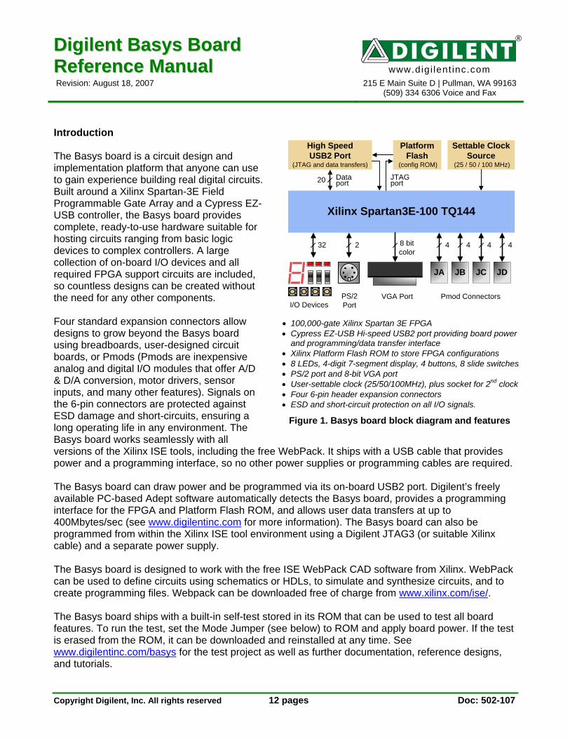
Introduction The Basys board is a circuit design and implementation platform that anyone can use to gain experience building real digital circuits. Built around a Xilinx Spartan-3E Field Programmable Gate Array and a Cypress EZ-USB controller, the Basys board provides complete, ready-to-use hardware suitable for hosting circuits ranging from basic logic devices to complex controllers. A large collection of on-board I/O devices and all required FPGA support circuits are included, so countless designs can be created without the need for any other components. Four standard expansion connectors allow designs to grow beyond the Basys board using breadboards, user-designed circuit boards, or Pmods (Pmods are inexpensive analog and digital I/O modules that offer A/D & D/A conversion, motor drivers, sensor inputs, and many other features). Signals on the 6-pin connectors are protected against ESD damage and short-circuits, ensuring a long operating life in any environment. The Basys board works seamlessly with all versions of the Xilinx ISE tools, including the free WebPack. It ships with a USB cable that provides power and a programming interface, so no other power supplies or programming cables are required. The Basys board can draw power and be programmed via its on-board USB2 port. Digilent’s freely available PC-based Adept software automatically detects the Basys board, provides a programming interface for the FPGA and Platform Flash ROM, and allows user data transfers at up to 400Mbytes/sec (see www.digilentinc.com for more information). The Basys board can also be programmed from within the Xilinx ISE tool environment using a Digilent JTAG3 (or suitable Xilinx cable) and a separate power supply. The Basys board is designed to work with the free ISE WebPack CAD software from Xilinx. WebPack can be used to define circuits using schematics or HDLs, to simulate and synthesize circuits, and to create programming files. Webpack can be downloaded free of charge from www.xilinx.com/ise/. The Basys board ships with a built-in self-test stored in its ROM that can be used to test all board features. To run the test, set the Mode Jumper (see below) to ROM and apply board power. If the test is erased from the ROM, it can be downloaded and reinstalled at any time. See www.digilentinc.com/basys for the test project as well as further documentation, reference designs, and tutorials.
Xilinx Spartan3E-100 TQ144
VGA Port
PlatformFlash
(config ROM)
Settable Clock Source
(25 / 50 / 100 MHz)
High SpeedUSB2 Port
(JTAG and data transfers)
20
JA JB JC JD
JTAGport
I/O DevicesPS/2Port
Pmod Connectors
44448 bit color
232
Dataport
• 100,000-gate Xilinx Spartan 3E FPGA • Cypress EZ-USB Hi-speed USB2 port providing board power
and programming/data transfer interface • Xilinx Platform Flash ROM to store FPGA configurations • 8 LEDs, 4-digit 7-segment display, 4 buttons, 8 slide switches • PS/2 port and 8-bit VGA port • User-settable clock (25/50/100MHz), plus socket for 2nd clock • Four 6-pin header expansion connectors • ESD and short-circuit protection on all I/O signals.
Figure 1. Basys board block diagram and features
Digilent Basys Reference Manual www.digilentinc.com
Copyright Digilent, Inc. Page 2/12 Doc: 502-107
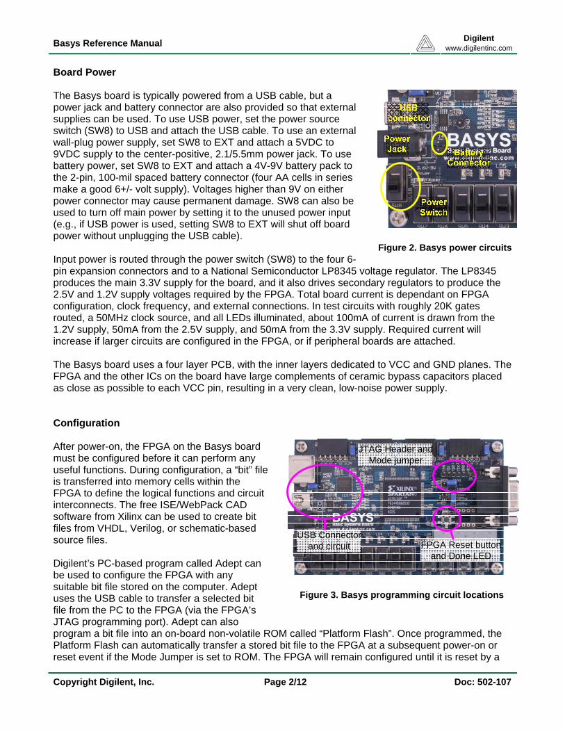
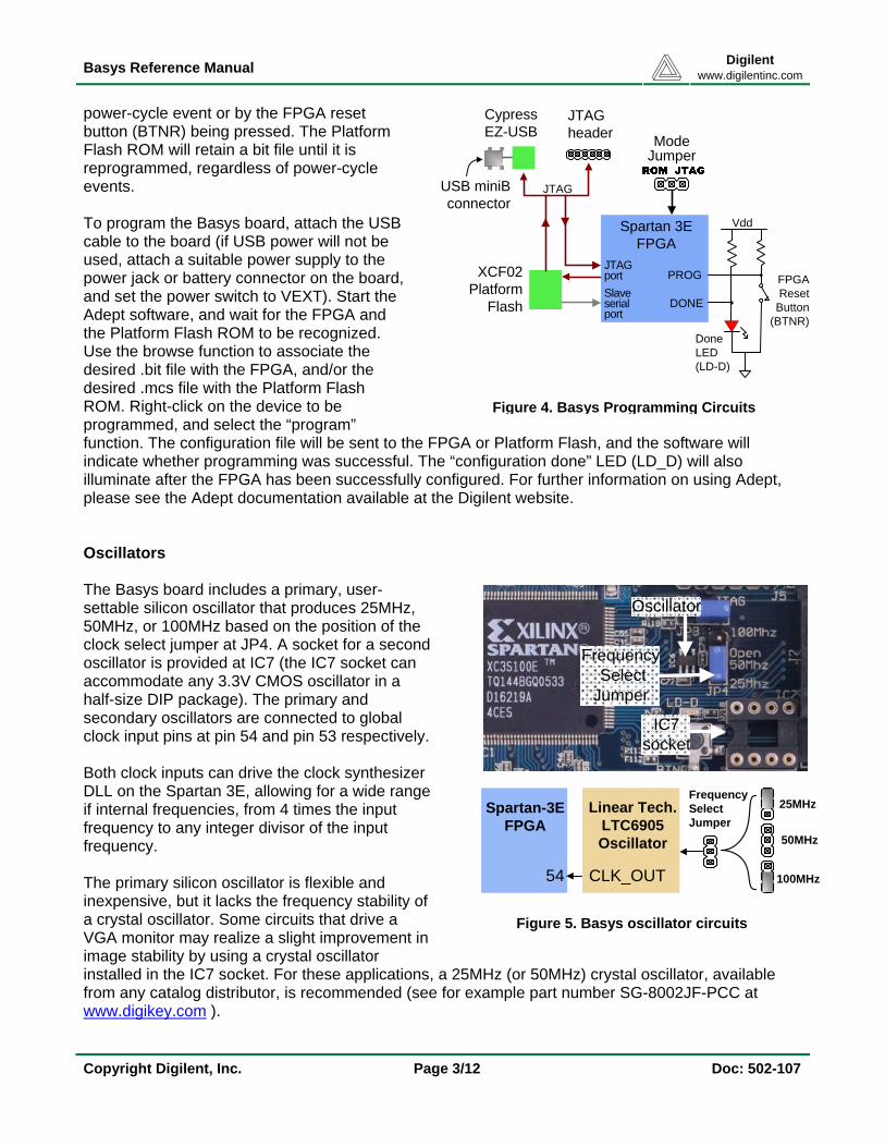
Board Power The Basys board is typically powered from a USB cable, but a power jack and battery connector are also provided so that external supplies can be used. To use USB power, set the power source switch (SW8) to USB and attach the USB cable. To use an external wall-plug power supply, set SW8 to EXT and attach a 5VDC to 9VDC supply to the center-positive, 2.1/5.5mm power jack. To use battery power, set SW8 to EXT and attach a 4V-9V battery pack to the 2-pin, 100-mil spaced battery connector (four AA cells in series make a good 6+/- volt supply). Voltages higher than 9V on either power connector may cause permanent damage. SW8 can also be used to turn off main power by setting it to the unused power input (e.g., if USB power is used, setting SW8 to EXT will shut off board power without unplugging the USB cable). Input power is routed through the power switch (SW8) to the four 6-pin expansion connectors and to a National Semiconductor LP8345 voltage regulator. The LP8345 produces the main 3.3V supply for the board, and it also drives secondary regulators to produce the 2.5V and 1.2V supply voltages required by the FPGA. Total board current is dependant on FPGA configuration, clock frequency, and external connections. In test circuits with roughly 20K gates routed, a 50MHz clock source, and all LEDs illuminated, about 100mA of current is drawn from the 1.2V supply, 50mA from the 2.5V supply, and 50mA from the 3.3V supply. Required current will increase if larger circuits are configured in the FPGA, or if peripheral boards are attached. The Basys board uses a four layer PCB, with the inner layers dedicated to VCC and GND planes. The FPGA and the other ICs on the board have large complements of ceramic bypass capacitors placed as close as possible to each VCC pin, resulting in a very clean, low-noise power supply. Configuration After power-on, the FPGA on the Basys board must be configured before it can perform any useful functions. During configuration, a “bit” file is transferred into memory cells within the FPGA to define the logical functions and circuit interconnects. The free ISE/WebPack CAD software from Xilinx can be used to create bit files from VHDL, Verilog, or schematic-based source files. Digilent’s PC-based program called Adept can be used to configure the FPGA with any suitable bit file stored on the computer. Adept uses the USB cable to transfer a selected bit file from the PC to the FPGA (via the FPGA’s JTAG programming port). Adept can also program a bit file into an on-board non-volatile ROM called “Platform Flash”. Once programmed, the Platform Flash can automatically transfer a stored bit file to the FPGA at a subsequent power-on or reset event if the Mode Jumper is set to ROM. The FPGA will remain configured until it is reset by a
Figure 2. Basys power circuits
FPGA Reset button and Done LED
USB Connector and circuit
JTAG Header and Mode jumper
Figure 3. Basys programming circuit locations
Digilent Basys Reference Manual www.digilentinc.com
Copyright Digilent, Inc. Page 3/12 Doc: 502-107
power-cycle event or by the FPGA reset button (BTNR) being pressed. The Platform Flash ROM will retain a bit file until it is reprogrammed, regardless of power-cycle events. To program the Basys board, attach the USB cable to the board (if USB power will not be used, attach a suitable power supply to the power jack or battery connector on the board, and set the power switch to VEXT). Start the Adept software, and wait for the FPGA and the Platform Flash ROM to be recognized. Use the browse function to associate the desired .bit file with the FPGA, and/or the desired .mcs file with the Platform Flash ROM. Right-click on the device to be programmed, and select the “program” function. The configuration file will be sent to the FPGA or Platform Flash, and the software will indicate whether programming was successful. The “configuration done” LED (LD_D) will also illuminate after the FPGA has been successfully configured. For further information on using Adept, please see the Adept documentation available at the Digilent website. Oscillators The Basys board includes a primary, user-settable silicon oscillator that produces 25MHz, 50MHz, or 100MHz based on the position of the clock select jumper at JP4. A socket for a second oscillator is provided at IC7 (the IC7 socket can accommodate any 3.3V CMOS oscillator in a half-size DIP package). The primary and secondary oscillators are connected to global clock input pins at pin 54 and pin 53 respectively. Both clock inputs can drive the clock synthesizer DLL on the Spartan 3E, allowing for a wide range if internal frequencies, from 4 times the input frequency to any integer divisor of the input frequency. The primary silicon oscillator is flexible and inexpensive, but it lacks the frequency stability of a crystal oscillator. Some circuits that drive a VGA monitor may realize a slight improvement in image stability by using a crystal oscillator installed in the IC7 socket. For these applications, a 25MHz (or 50MHz) crystal oscillator, available from any catalog distributor, is recommended (see for example part number SG-8002JF-PCC at www.digikey.com ).
Spartan-3EFPGA
54 CLK_OUT
Linear Tech.LTC6905Oscillator
Frequency Select Jumper
25MHz
50MHz
100MHz
Frequency SelectJumper
Oscillator
IC7socket
Figure 5. Basys oscillator circuits
XCF02Platform
Flash
JTAGheader
JTAG
PROG
DONE
Vdd
DoneLED(LD-D)
FPGAReset
Button(BTNR)
Spartan 3EFPGA
ModeJumper
USB miniBconnector
CypressEZ-USB
Slaveserialport
JTAGport
Figure 4. Basys Programming Circuits
Digilent Basys Reference Manual www.digilentinc.com
Copyright Digilent, Inc. Page 4/12 Doc: 502-107
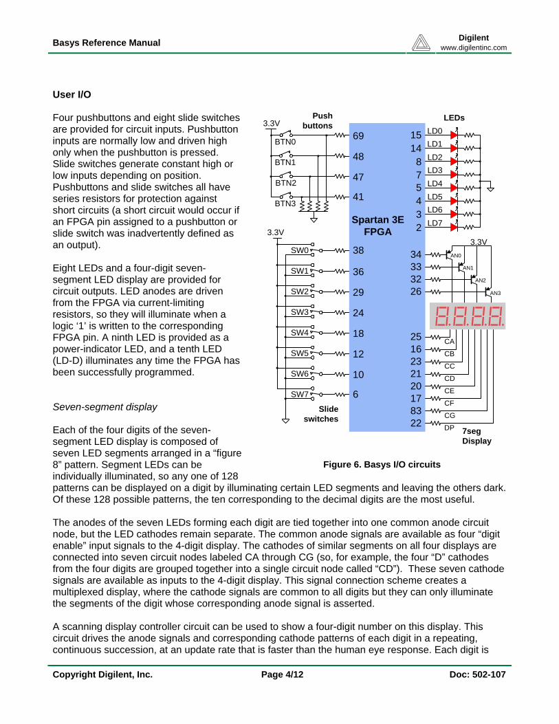
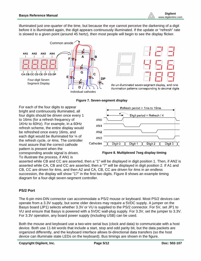
User I/O Four pushbuttons and eight slide switches are provided for circuit inputs. Pushbutton inputs are normally low and driven high only when the pushbutton is pressed. Slide switches generate constant high or low inputs depending on position. Pushbuttons and slide switches all have series resistors for protection against short circuits (a short circuit would occur if an FPGA pin assigned to a pushbutton or slide switch was inadvertently defined as an output). Eight LEDs and a four-digit seven-segment LED display are provided for circuit outputs. LED anodes are driven from the FPGA via current-limiting resistors, so they will illuminate when a logic ‘1’ is written to the corresponding FPGA pin. A ninth LED is provided as a power-indicator LED, and a tenth LED (LD-D) illuminates any time the FPGA has been successfully programmed. Seven-segment display Each of the four digits of the seven-segment LED display is composed of seven LED segments arranged in a “figure 8” pattern. Segment LEDs can be individually illuminated, so any one of 128 patterns can be displayed on a digit by illuminating certain LED segments and leaving the others dark. Of these 128 possible patterns, the ten corresponding to the decimal digits are the most useful. The anodes of the seven LEDs forming each digit are tied together into one common anode circuit node, but the LED cathodes remain separate. The common anode signals are available as four “digit enable” input signals to the 4-digit display. The cathodes of similar segments on all four displays are connected into seven circuit nodes labeled CA through CG (so, for example, the four “D” cathodes from the four digits are grouped together into a single circuit node called “CD”). These seven cathode signals are available as inputs to the 4-digit display. This signal connection scheme creates a multiplexed display, where the cathode signals are common to all digits but they can only illuminate the segments of the digit whose corresponding anode signal is asserted. A scanning display controller circuit can be used to show a four-digit number on this display. This circuit drives the anode signals and corresponding cathode patterns of each digit in a repeating, continuous succession, at an update rate that is faster than the human eye response. Each digit is
3.3VPush
buttons
Slideswitches
Spartan 3E FPGA
47
48
69
29
24
18
12
10
41
6
BTN0
BTN1
BTN2
BTN3
SW0
SW1
SW2
SW3
SW4
SW5
SW6
SW7
3.3V
LD0LD1LD2LD3LD4LD5LD6LD7
3.3V
LEDs
7segDisplay
AN0
AN1
AN2
AN3
36
38
1514
875432
34333226
25162321201783
CA
CB
CC
CD
CE
CF
CG
DP22
Figure 6. Basys I/O circuits
Digilent Basys Reference Manual www.digilentinc.com
Copyright Digilent, Inc. Page 5/12 Doc: 502-107
illuminated just one-quarter of the time, but because the eye cannot perceive the darkening of a digit before it is illuminated again, the digit appears continuously illuminated. If the update or “refresh” rate is slowed to a given point (around 45 hertz), then most people will begin to see the display flicker.
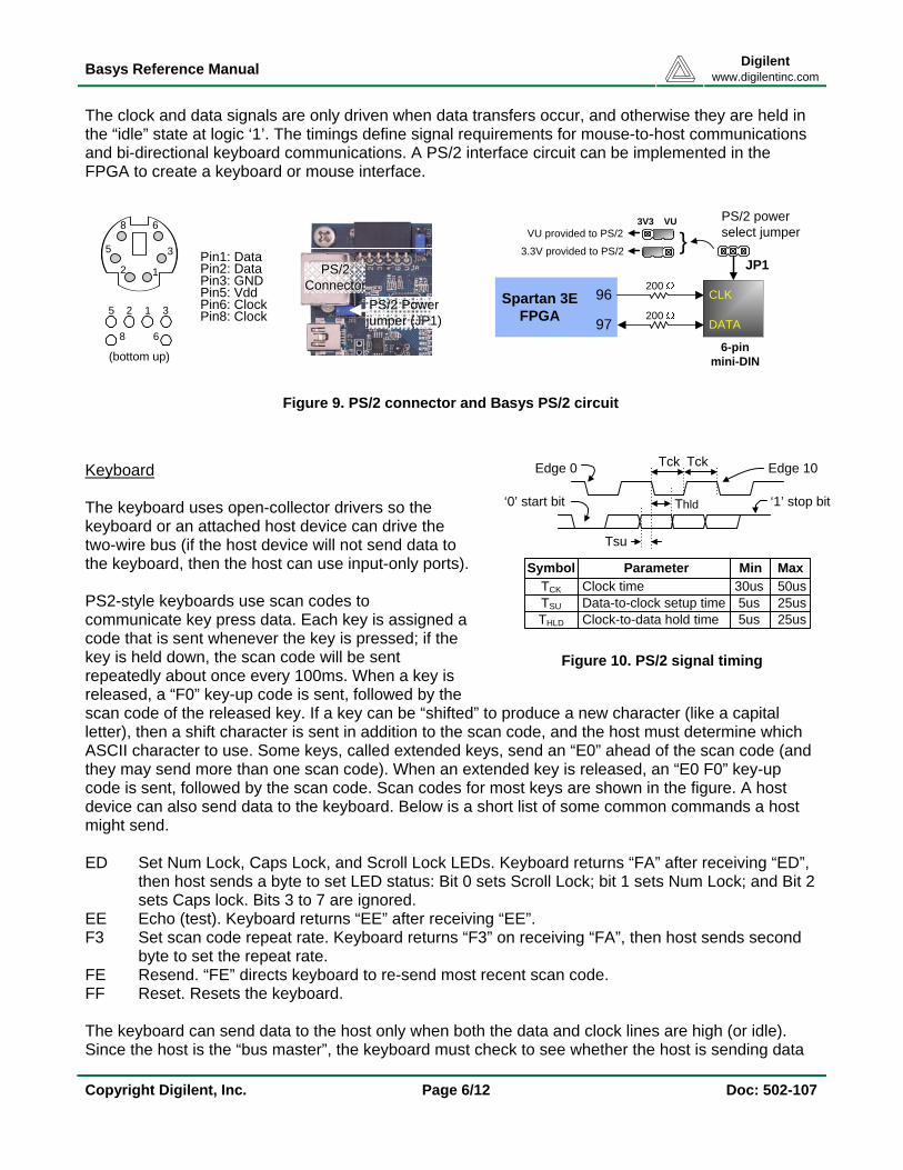
For each of the four digits to appear bright and continuously illuminated, all four digits should be driven once every 1 to 16ms (for a refresh frequency of 1KHz to 60Hz). For example, in a 60Hz refresh scheme, the entire display would be refreshed once every 16ms, and each digit would be illuminated for ¼ of the refresh cycle, or 4ms. The controller must assure that the correct cathode pattern is present when the corresponding anode signal is driven. To illustrate the process, if AN1 is asserted while CB and CC are asserted, then a “1” will be displayed in digit position 1. Then, if AN2 is asserted while CA, CB and CC are asserted, then a “7” will be displayed in digit position 2. If A1 and CB, CC are driven for 4ms, and then A2 and CA, CB, CC are driven for 4ms in an endless succession, the display will show “17” in the first two digits. Figure 8 shows an example timing diagram for a four-digit seven-segment controller. PS/2 Port The 6-pin mini-DIN connector can accommodate a PS/2 mouse or keyboard. Most PS/2 devices can operate from a 3.3V supply, but some older devices may require a 5VDC supply. A jumper on the Basys board (JP1) selects whether 3.3V or VU is supplied to the PS/2 connector. For 5V, set JP1 to VU and ensure that Basys is powered with a 5VDC wall-plug supply. For 3.3V, set the jumper to 3.3V. For 3.3V operation, any board power supply (including USB) can be used. Both the mouse and keyboard use a two-wire serial bus (clock and data) to communicate with a host device. Both use 11-bit words that include a start, stop and odd parity bit, but the data packets are organized differently, and the keyboard interface allows bi-directional data transfers (so the host device can illuminate state LEDs on the keyboard). Bus timings are shown in the figure.
Figure 8. Multiplexed 7seg display timing
AF
E
D
C
B
G
Common anode
Individual cathodes
DP
AN1 AN2 AN3 AN4
CA CB CC CD CE CF CG DP
Four-digit Seven Segment Display
Figure 7. Seven-segment display
Digilent Basys Reference Manual www.digilentinc.com
Copyright Digilent, Inc. Page 6/12 Doc: 502-107
The clock and data signals are only driven when data transfers occur, and otherwise they are held in the “idle” state at logic ‘1’. The timings define signal requirements for mouse-to-host communications and bi-directional keyboard communications. A PS/2 interface circuit can be implemented in the FPGA to create a keyboard or mouse interface.
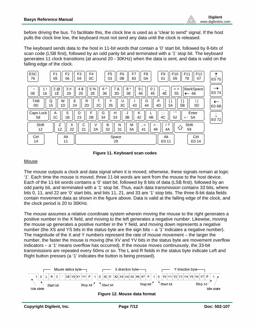
Keyboard The keyboard uses open-collector drivers so the keyboard or an attached host device can drive the two-wire bus (if the host device will not send data to the keyboard, then the host can use input-only ports). PS2-style keyboards use scan codes to communicate key press data. Each key is assigned a code that is sent whenever the key is pressed; if the key is held down, the scan code will be sent repeatedly about once every 100ms. When a key is released, a “F0” key-up code is sent, followed by the scan code of the released key. If a key can be “shifted” to produce a new character (like a capital letter), then a shift character is sent in addition to the scan code, and the host must determine which ASCII character to use. Some keys, called extended keys, send an “E0” ahead of the scan code (and they may send more than one scan code). When an extended key is released, an “E0 F0” key-up code is sent, followed by the scan code. Scan codes for most keys are shown in the figure. A host device can also send data to the keyboard. Below is a short list of some common commands a host might send. ED Set Num Lock, Caps Lock, and Scroll Lock LEDs. Keyboard returns “FA” after receiving “ED”,
then host sends a byte to set LED status: Bit 0 sets Scroll Lock; bit 1 sets Num Lock; and Bit 2 sets Caps lock. Bits 3 to 7 are ignored.
EE Echo (test). Keyboard returns “EE” after receiving “EE”. F3 Set scan code repeat rate. Keyboard returns “F3” on receiving “FA”, then host sends second
byte to set the repeat rate. FE Resend. “FE” directs keyboard to re-send most recent scan code. FF Reset. Resets the keyboard. The keyboard can send data to the host only when both the data and clock lines are high (or idle). Since the host is the “bus master”, the keyboard must check to see whether the host is sending data
TCK
TSU
Clock timeData-to-clock setup time
30us5us
50us25us
Symbol Parameter Min Max
THLD Clock-to-data hold time 5us 25us
Edge 0
‘0’ start bit ‘1’ stop bit
Edge 10
Tsu
Thld
Tck Tck
Figure 10. PS/2 signal timing
Pin1: DataPin2: DataPin3: GNDPin5: VddPin6: ClockPin8: Clock2 1 35
8 6
1
3
6
2
5
8
(bottom up)
PS/2 Connector
PS/2 Power jumper (JP1)
96Spartan 3EFPGA
CLK
DATA
6-pin mini-DIN
97
200
200
PS/2 power select jumper
VU
3.3V provided to PS/2
VU provided to PS/2 }JP1
3V3
Figure 9. PS/2 connector and Basys PS/2 circuit
Digilent Basys Reference Manual www.digilentinc.com
Copyright Digilent, Inc. Page 7/12 Doc: 502-107
before driving the bus. To facilitate this, the clock line is used as a “clear to send” signal. If the host pulls the clock line low, the keyboard must not send any data until the clock is released. The keyboard sends data to the host in 11-bit words that contain a ‘0’ start bit, followed by 8-bits of scan code (LSB first), followed by an odd parity bit and terminated with a ‘1’ stop bit. The keyboard generates 11 clock transitions (at around 20 - 30KHz) when the data is sent, and data is valid on the falling edge of the clock.
Mouse The mouse outputs a clock and data signal when it is moved; otherwise, these signals remain at logic ‘1’. Each time the mouse is moved, three 11-bit words are sent from the mouse to the host device. Each of the 11-bit words contains a ‘0’ start bit, followed by 8 bits of data (LSB first), followed by an odd parity bit, and terminated with a ‘1’ stop bit. Thus, each data transmission contains 33 bits, where bits 0, 11, and 22 are ‘0’ start bits, and bits 11, 21, and 33 are ‘1’ stop bits. The three 8-bit data fields contain movement data as shown in the figure above. Data is valid at the falling edge of the clock, and the clock period is 20 to 30KHz. The mouse assumes a relative coordinate system wherein moving the mouse to the right generates a positive number in the X field, and moving to the left generates a negative number. Likewise, moving the mouse up generates a positive number in the Y field, and moving down represents a negative number (the XS and YS bits in the status byte are the sign bits – a ‘1’ indicates a negative number). The magnitude of the X and Y numbers represent the rate of mouse movement – the larger the number, the faster the mouse is moving (the XV and YV bits in the status byte are movement overflow indicators – a ‘1’ means overflow has occurred). If the mouse moves continuously, the 33-bit transmissions are repeated every 50ms or so. The L and R fields in the status byte indicate Left and Right button presses (a ‘1’ indicates the button is being pressed).
ESC76
` ~0E
TAB0D
Caps Lock58
Shift12
Ctrl14
1 !16
2 @1E
3 #26
4 $25
5 %2E
Q15
W1D
E24
R2D
T2C
A1C
S1B
D23
F2B
G34
Z1Z
X22
C21
V2A
B32
6 ^36
7 &3D
8 *3E
9 (46
0 )45
- _4E
= +55
BackSpace66
Y35
U3C
I43
O44
P4D
[ {54
] }5B
\ |5D
H33
J3B
K42
L4B
; :4C
' "52
Enter5A
N31
M3A
, <41
> .49
/ ?4A
Shift59
Alt11
Space29
AltE0 11
CtrlE0 14
F105
F206
F304
F40C
F503
F60B
F783
F80A
F901
F1009
F1178
F1207 E0 75
E0 74
E0 6B
E0 72
Figure 11. Keyboard scan codes
Figure 12. Mouse data format
Digilent Basys Reference Manual www.digilentinc.com
Copyright Digilent, Inc. Page 8/12 Doc: 502-107
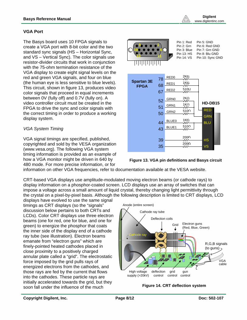
VGA Port The Basys board uses 10 FPGA signals to create a VGA port with 8-bit color and the two standard sync signals (HS – Horizontal Sync, and VS – Vertical Sync). The color signals use resistor-divider circuits that work in conjunction with the 75-ohm termination resistance of the VGA display to create eight signal levels on the red and green VGA signals, and four on blue (the human eye is less sensitive to blue levels). This circuit, shown in figure 13, produces video color signals that proceed in equal increments between 0V (fully off) and 0.7V (fully on). A video controller circuit must be created in the FPGA to drive the sync and color signals with the correct timing in order to produce a working display system. VGA System Timing VGA signal timings are specified, published, copyrighted and sold by the VESA organization (www.vesa.org). The following VGA system timing information is provided as an example of how a VGA monitor might be driven in 640 by 480 mode. For more precise information, or for information on other VGA frequencies, refer to documentation available at the VESA website. CRT-based VGA displays use amplitude-modulated moving electron beams (or cathode rays) to display information on a phosphor-coated screen. LCD displays use an array of switches that can impose a voltage across a small amount of liquid crystal, thereby changing light permittivity through the crystal on a pixel-by-pixel basis. Although the following description is limited to CRT displays, LCD displays have evolved to use the same signal timings as CRT displays (so the “signals” discussion below pertains to both CRTs and LCDs). Color CRT displays use three electron beams (one for red, one for blue, and one for green) to energize the phosphor that coats the inner side of the display end of a cathode ray tube (see illustration). Electron beams emanate from “electron guns” which are finely-pointed heated cathodes placed in close proximity to a positively charged annular plate called a “grid”. The electrostatic force imposed by the grid pulls rays of energized electrons from the cathodes, and those rays are fed by the current that flows into the cathodes. These particle rays are initially accelerated towards the grid, but they soon fall under the influence of the much
78Spartan 3EFPGA
HD-DB15
6867
3935
2K
1K
510
200
200
1510
5
116
1Pin 1: RedPin 2: GrnPin 3: BluePin 13: HSPin 14: VS
Pin 5: GNDPin 6: Red GNDPin 7: Grn GNDPin 8: Blu GNDPin 10: Sync GND
RED0
RED1
RED2
525150
2K
1K
510
GRN0
GRN1
GRN2
4443
1K
510
BLUE0
BLUE1
RED
GRN
BLU
HS
VS
Figure 13. VGA pin definitions and Basys circuit
Anode (entire screen)
High voltage supply (>20kV)
Deflection coils
Grid Electron guns(Red, Blue, Green)
guncontrol
gridcontrol
deflectioncontrol
R,G,B signals (to guns)
Cathode ray tube
Cathode ray
VGA cable
Figure 14. CRT deflection system
Digilent Basys Reference Manual www.digilentinc.com
Copyright Digilent, Inc. Page 9/12 Doc: 502-107
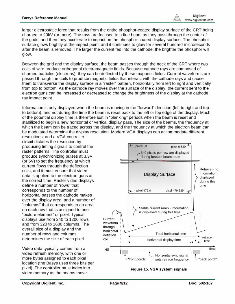
larger electrostatic force that results from the entire phosphor-coated display surface of the CRT being charged to 20kV (or more). The rays are focused to a fine beam as they pass through the center of the grids, and then they accelerate to impact on the phosphor-coated display surface. The phosphor surface glows brightly at the impact point, and it continues to glow for several hundred microseconds after the beam is removed. The larger the current fed into the cathode, the brighter the phosphor will glow. Between the grid and the display surface, the beam passes through the neck of the CRT where two coils of wire produce orthogonal electromagnetic fields. Because cathode rays are composed of charged particles (electrons), they can be deflected by these magnetic fields. Current waveforms are passed through the coils to produce magnetic fields that interact with the cathode rays and cause them to transverse the display surface in a “raster” pattern, horizontally from left to right and vertically from top to bottom. As the cathode ray moves over the surface of the display, the current sent to the electron guns can be increased or decreased to change the brightness of the display at the cathode ray impact point. Information is only displayed when the beam is moving in the “forward” direction (left to right and top to bottom), and not during the time the beam is reset back to the left or top edge of the display. Much of the potential display time is therefore lost in “blanking” periods when the beam is reset and stabilized to begin a new horizontal or vertical display pass. The size of the beams, the frequency at which the beam can be traced across the display, and the frequency at which the electron beam can be modulated determine the display resolution. Modern VGA displays can accommodate different resolutions, and a VGA controller circuit dictates the resolution by producing timing signals to control the raster patterns. The controller must produce synchronizing pulses at 3.3V (or 5V) to set the frequency at which current flows through the deflection coils, and it must ensure that video data is applied to the electron guns at the correct time. Raster video displays define a number of “rows” that corresponds to the number of horizontal passes the cathode makes over the display area, and a number of “columns” that corresponds to an area on each row that is assigned to one “picture element” or pixel. Typical displays use from 240 to 1200 rows and from 320 to 1600 columns. The overall size of a display and the number of rows and columns determines the size of each pixel. Video data typically comes from a video refresh memory, with one or more bytes assigned to each pixel location (the Basys uses three bits per pixel). The controller must index into video memory as the beams move
Currentwaveform through horizontal defletion coil
Stable current ramp - information is displayed during this time
Retrace - no information displayed during this time
Total horizontal time
Horizontal display time
Horizontal sync signal sets retrace frequency
retrace time
timeHS
"back porch""front porch"
Display Surface
640 pixels per row are displayedduring forward beam trace
pixel 0,639pixel 0,0
pixel 479,0 pixel 479,639
Figure 15. VGA system signals
Digilent Basys Reference Manual www.digilentinc.com
Copyright Digilent, Inc. Page 10/12 Doc: 502-107
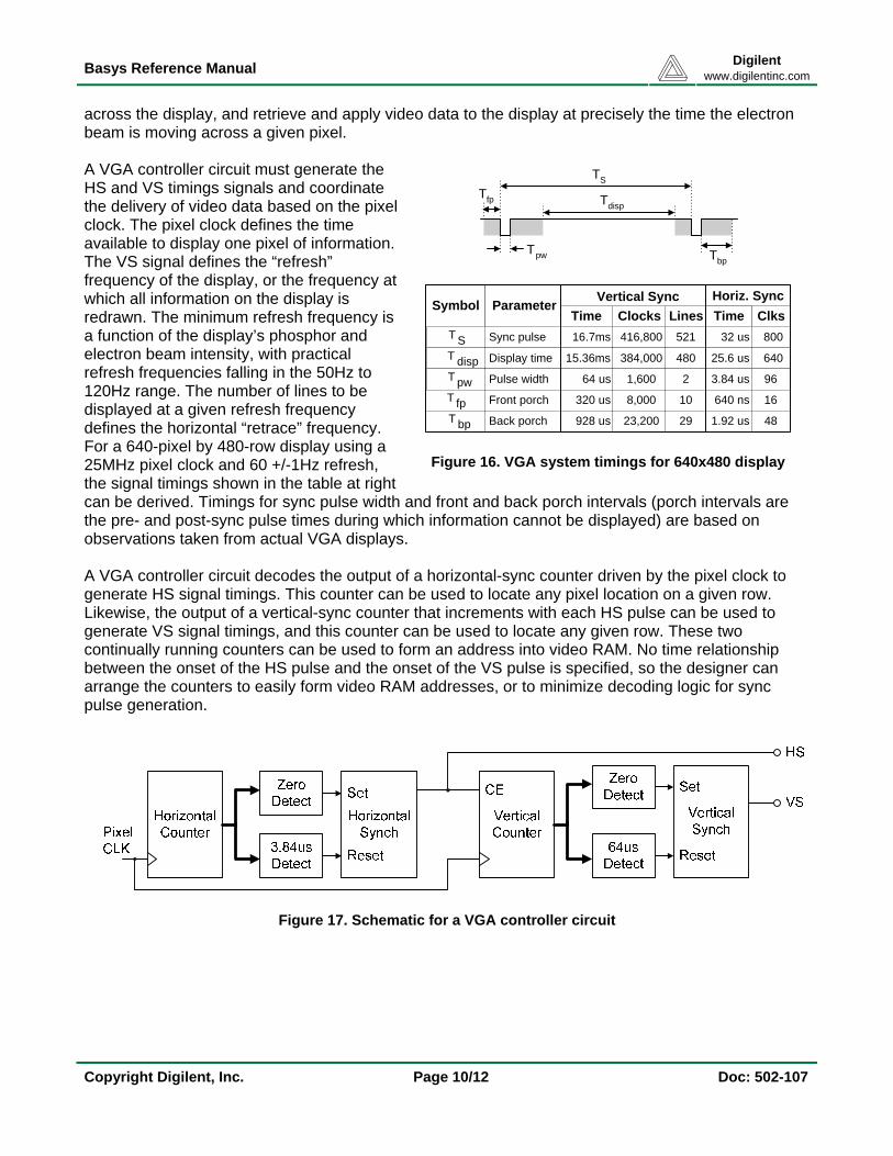
across the display, and retrieve and apply video data to the display at precisely the time the electron beam is moving across a given pixel. A VGA controller circuit must generate the HS and VS timings signals and coordinate the delivery of video data based on the pixel clock. The pixel clock defines the time available to display one pixel of information. The VS signal defines the “refresh” frequency of the display, or the frequency at which all information on the display is redrawn. The minimum refresh frequency is a function of the display’s phosphor and electron beam intensity, with practical refresh frequencies falling in the 50Hz to 120Hz range. The number of lines to be displayed at a given refresh frequency defines the horizontal “retrace” frequency. For a 640-pixel by 480-row display using a 25MHz pixel clock and 60 +/-1Hz refresh, the signal timings shown in the table at right can be derived. Timings for sync pulse width and front and back porch intervals (porch intervals are the pre- and post-sync pulse times during which information cannot be displayed) are based on observations taken from actual VGA displays. A VGA controller circuit decodes the output of a horizontal-sync counter driven by the pixel clock to generate HS signal timings. This counter can be used to locate any pixel location on a given row. Likewise, the output of a vertical-sync counter that increments with each HS pulse can be used to generate VS signal timings, and this counter can be used to locate any given row. These two continually running counters can be used to form an address into video RAM. No time relationship between the onset of the HS pulse and the onset of the VS pulse is specified, so the designer can arrange the counters to easily form video RAM addresses, or to minimize decoding logic for sync pulse generation.
TS
Tdisp
Tpw
Tfp
Tbp
T ST dispT pwT fpT bp
Sync pulse
Display time
Pulse width
Front porch
Back porch
16.7ms
15.36ms
64 us
320 us
928 us
416,800
384,000
1,600
8,000
23,200
521
480
2
10
29
Symbol ParameterTime Clocks Lines
Vertical Sync
32 us
25.6 us
3.84 us
640 ns
1.92 us
800
640
96
16
48
ClksHoriz. SyncTime
Figure 16. VGA system timings for 640x480 display
Figure 17. Schematic for a VGA controller circuit
Digilent Basys Reference Manual www.digilentinc.com
Copyright Digilent, Inc. Page 11/12 Doc: 502-107
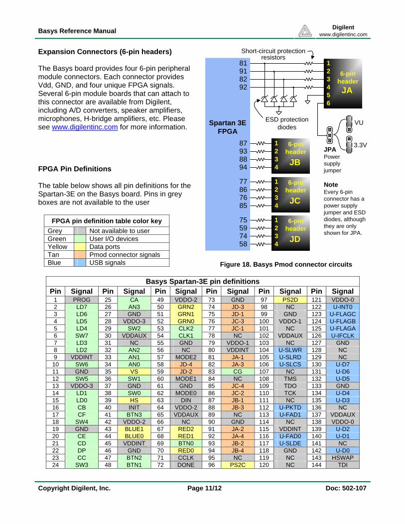
Expansion Connectors (6-pin headers) The Basys board provides four 6-pin peripheral module connectors. Each connector provides Vdd, GND, and four unique FPGA signals. Several 6-pin module boards that can attach to this connector are available from Digilent, including A/D converters, speaker amplifiers, microphones, H-bridge amplifiers, etc. Please see www.digilentinc.com for more information. FPGA Pin Definitions The table below shows all pin definitions for the Spartan-3E on the Basys board. Pins in grey boxes are not available to the user
FPGA pin definition table color key Grey Not available to user Green User I/O devices Yellow Data ports Tan Pmod connector signals Blue USB signals
Basys Spartan-3E pin definitions
Pin Signal Pin Signal Pin Signal Pin Signal Pin Signal Pin Signal 1 PROG 25 CA 49 VDDO-2 73 GND 97 PS2D 121 VDDO-0 2 LD7 26 AN3 50 GRN2 74 JD-3 98 NC 122 U-INT0 3 LD6 27 GND 51 GRN1 75 JD-1 99 GND 123 U-FLAGC 4 LD5 28 VDDO-3 52 GRN0 76 JC-3 100 VDDO-1 124 U-FLAGB 5 LD4 29 SW2 53 CLK2 77 JC-1 101 NC 125 U-FLAGA 6 SW7 30 VDDAUX 54 CLK1 78 NC 102 VDDAUX 126 U-IFCLK 7 LD3 31 NC 55 GND 79 VDDO-1 103 NC 127 GND 8 LD2 32 AN2 56 NC 80 VDDINT 104 U-SLWR 128 NC 9 VDDINT 33 AN1 57 MODE2 81 JA-1 105 U-SLRD 129 NC 10 SW6 34 AN0 58 JD-4 82 JA-3 106 U-SLCS 130 U-D7 11 GND 35 VS 59 JD-2 83 CG 107 NC 131 U-D6 12 SW5 36 SW1 60 MODE1 84 NC 108 TMS 132 U-D5 13 VDDO-3 37 GND 61 GND 85 JC-4 109 TDO 133 GND 14 LD1 38 SW0 62 MODE0 86 JC-2 110 TCK 134 U-D4 15 LD0 39 HS 63 DIN 87 JB-1 111 NC 135 U-D3 16 CB 40 INIT 64 VDDO-2 88 JB-3 112 U-PKTD 136 NC 17 CF 41 BTN3 65 VDDAUX 89 NC 113 U-FAD1 137 VDDAUX 18 SW4 42 VDDO-2 66 NC 90 GND 114 NC 138 VDDO-0 19 GND 43 BLUE1 67 RED2 91 JA-2 115 VDDINT 139 U-D2 20 CE 44 BLUE0 68 RED1 92 JA-4 116 U-FAD0 140 U-D1 21 CD 45 VDDINT 69 BTN0 93 JB-2 117 U-SLDE 141 NC 22 DP 46 GND 70 RED0 94 JB-4 118 GND 142 U-D0 23 CC 47 BTN2 71 CCLK 95 NC 119 NC 143 HSWAP 24 SW3 48 BTN1 72 DONE 96 PS2C 120 NC 144 TDI
Spartan 3EFPGA
81918292
ESD protection diodes
16-pin
header23456
JA
Short-circuit protection resistors
VU
3.3VJPAPower supply jumper
1 6-pinheader2
34 JB
1 6-pinheader2
34 JC
1 6-pinheader2
34 JD
87938894
77867685
75597458
NoteEvery 6-pin connector has a power supply jumper and ESD diodes, although they are only shown for JPA.
Figure 18. Basys Pmod connector circuits
Digilent Basys Reference Manual www.digilentinc.com
Copyright Digilent, Inc. Page 12/12 Doc: 502-107
Built in Self Test A demonstration configuration is loaded into the Platform Flash ROM during manufacturing. This demo, also available on the resource CD and on the Digilent website, can serve as a board verification test since it interacts with all devices and ports on the Basys board. To configure the FPGA from a bit file stored in Platform Flash, set the Mode Jumper to ROM and cycle power or press the FPGA reset button (BTNR). The self-test connects the switches to the LEDs, the buttons and PS/2 keyboard (if attached) to the seven-segment display, and a VGA monitor (if attached) will show a color pattern. By interacting with the buttons and switches on the Basys board (and the keys on a PS/2 keyboard if attached), and watching the LEDs, seven-segment display, and VGA monitor (if attached), any hardware problems with the Basys board can be readily identified. If the self test is not resident in the Platform Flash ROM, it can be programmed into the FPGA or reloaded into the ROM using the Adept programming software.