Embed Size (px)
Citation preview
JY213H
High Voltage 3-Phase Gate Driver
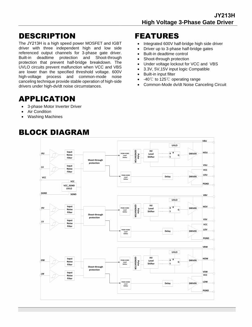
DESCRIPTION
The JY213H is a high speed power MOSFET and IGBT driver with three independent high and low side referenced output channels for 3-phase gate driver. Built-in deadtime protection and Shoot-through protection that prevent half-bridge breakdown. The UVLO circuits prevent malfunction when VCC and VBS are lower than the specified threshold voltage. 600V high-voltage process and common-mode noise canceling technique provide stable operation of high-side drivers under high-dv/dt noise circumstances.
APPLICATION
3-phase Motor Inverter Driver
Air Condition
Washing Machines
FEATURES
Integrated 600V half-bridge high side driver
Driver up to 3-phase half-bridge gates
Built-in deadtime control
Shoot-through protection
Under voltage lockout for VCC and VBS
3.3V, 5V,15V input logic Compatible
Built-in input filter
-40℃ to 125℃ operating range
Common-Mode dv/dt Noise Canceling Circuit
BLOCK DIAGRAM
Shoot-through protection
UVLO
R R
SQ
DRIVERHV
LevelShifter
Pu
lseG
ENER
ATO
R
Delay DRIVER
InputNoiseFilter
InputNoiseFilter
VBU
HOU
VSU
VCC
LOU
PGND
HU
LU
Shoot-through protection
InputNoiseFilter
InputNoiseFilter
VBV
HOV
VSV
VCC
LOV
PGND
HV
LV
Shoot-through protection
InputNoiseFilter
InputNoiseFilter
VBW
HOW
VSW
VCC
LOW
PGND
HW
LW
PGND-SGNDLevel
Shifter
PGND-SGNDLevel
Shifter
UVLO
R R
SQ
DRIVERHV
LevelShifter
Pu
lseG
ENER
ATO
R
Delay DRIVER
PGND-SGNDLevel
Shifter
PGND-SGNDLevel
Shifter
UVLO
R R
SQ
DRIVERHV
LevelShifter
Pu
lseG
ENER
ATO
R
Delay DRIVER
PGND-SGNDLevel
Shifter
PGND-SGNDLevel
Shifter
VCC_SGNDUVLO
VCC
SGNDSGND
VCC

JY213H
V1.0 2 August 2013
TYPICAL APPLICATION CIRCUIT
1
2
3
4
5
6
7
VCC
SGND
MCULOGIC
HOU
JY213H
VCC
Vmotor
Motor
8
9
12
11
10
13
14 15
16
17
18
19
20
21
22
23
24
25
26
27
28
HU
HV
HW
LU
LV
LW
NC.
PGND
LOW LOV
LOU
VSW
HOW
VBW
VSV
HOV
VBV
VSU
HOU
VBU
NC.
NC.
NC.NC.
U
V W
HOV HOW
LOU LOV LOW
NC.
V5V

JY213H
V1.0 3 August 2013
ORDER INFORMATION
Valid Part Number Package Type Top Code
JY213H-S 20-PIN, SOP, 300mil JY213H-S
JY213H-S1 24-PIN, SOP, 300mil JY213H-S1
JY213H-S2 28-PIN, SOP, 300mil JY213H-S2
PIN CONFIGURATION
20-PIN 24-PIN
PIN DESCRIPTION
Pin Name Description Pin No.
SOP20 SOP24
VCC Logic and low-side gate drivers power supply voltage 1 1
V5V 5V LDO output 2
HU Logic input for high-side gate U-phase driver 2 3
HV Logic input for high-side gate V-phase driver 3 4
HW Logic input for high-side gate W-phase driver 4 5
LU Logic input for low-side gate U-phase driver 5 6
LV Logic input for low-side gate V-phase driver 6 7
LW Logic input for low-side gate W-phase driver 7 8
GND Logic ground and low-side gate drivers ground 8 9
LOW Low-side gate driver W-phase output 9 10
LOV Low-side gate driver V-phase output 10 11
LOU Low-side gate driver U-phase output 11 12
NC. Not Connected 13
VSW High-side driver W-phase floating supply offset voltage 12 14
HOW High-side driver W-phase gate driver output 13 15
VBW High-side driver W-phase floating supply 14 16
NC. Not Connected 17
VSV High-side driver V-phase floating supply offset voltage 15 18
HOV High-side driver V-phase gate driver output 16 19
VBV High-side driver V-phase floating supply 17 20
NC. Not Connected 21
VSU High-side driver U-phase floating supply offset voltage 18 22
HOU High-side driver U-phase gate driver output 19 23
VBU High-side driver U-phase floating supply 20 24
JY213H-S
JY213H-S1

JY213H
V1.0 4 August 2013
28-PIN
PIN DESCRIPTION
Pin Name Description Pin No.
VCC Logic and low-side gate drivers power supply voltage 1
V5V 5V LDO output 2
NC. Not Connected 3
SGND Logic ground 4
HU Logic input for high-side gate U-phase driver 5
HV Logic input for high-side gate V-phase driver 6
HW Logic input for high-side gate W-phase driver 7
LU Logic input for low-side gate U-phase driver 8
LV Logic input for low-side gate V-phase driver 9
LW Logic input for low-side gate W-phase driver 10
NC. Not Connected 11
NC. Not Connected 12
PGND Low-side gate drivers ground 13
LOW Low-side gate driver W-phase output 14
LOV Low-side gate driver V-phase output 15
LOU Low-side gate driver U-phase output 16
NC. Not Connected 17
VSW High-side driver W-phase floating supply offset voltage 18
HOW High-side driver W-phase gate driver output 19
VBW High-side driver W-phase floating supply 20
NC. Not Connected 21
VSV High-side driver V-phase floating supply offset voltage 22
HOV High-side driver V-phase gate driver output 23
VBV High-side driver V-phase floating supply 24
NC. Not Connected 25
VSU High-side driver U-phase floating supply offset voltage 26
HOU High-side driver U-phase gate driver output 27
VBU High-side driver U-phase floating supply 28
JY213H-S2
JY213H
V1.0 5 August 2013
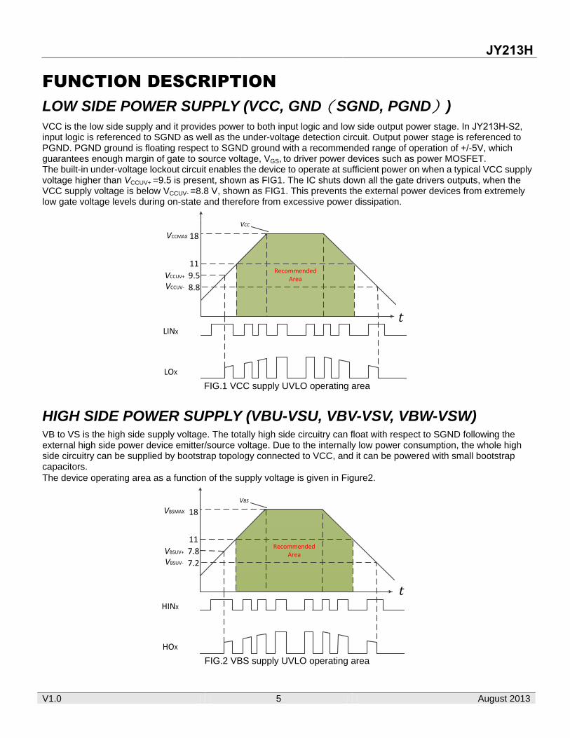
FUNCTION DESCRIPTION
LOW SIDE POWER SUPPLY (VCC, GND(SGND, PGND))
VCC is the low side supply and it provides power to both input logic and low side output power stage. In JY213H-S2, input logic is referenced to SGND as well as the under-voltage detection circuit. Output power stage is referenced to PGND. PGND ground is floating respect to SGND ground with a recommended range of operation of +/-5V, which guarantees enough margin of gate to source voltage, VGS, to driver power devices such as power MOSFET. The built-in under-voltage lockout circuit enables the device to operate at sufficient power on when a typical VCC supply voltage higher than VCCUV+ =9.5 is present, shown as FIG1. The IC shuts down all the gate drivers outputs, when the VCC supply voltage is below VCCUV- =8.8 V, shown as FIG1. This prevents the external power devices from extremely low gate voltage levels during on-state and therefore from excessive power dissipation.
VCCMAX
VCC
18
11
9.5
8.8
VCCUV+
VCCUV-
tLINX
LOX
RecommendedArea
FIG.1 VCC supply UVLO operating area
HIGH SIDE POWER SUPPLY (VBU-VSU, VBV-VSV, VBW-VSW) VB to VS is the high side supply voltage. The totally high side circuitry can float with respect to SGND following the external high side power device emitter/source voltage. Due to the internally low power consumption, the whole high side circuitry can be supplied by bootstrap topology connected to VCC, and it can be powered with small bootstrap capacitors.
The device operating area as a function of the supply voltage is given in Figure2.
VBSMAX
VBS
18
11
7.8
7.2
VBSUV+
VBSUV-
tHINX
HOX
RecommendedArea
FIG.2 VBS supply UVLO operating area

JY213H
V1.0 6 August 2013
LOW SIDE AND HIGH CONTROL INPUT LOGIC (HU, V, W / LU, V, W) The Schmitt trigger threshold of each input is designed enough low such to guarantee LSTTL and CMOS compatibility
down to 3.3 V controller outputs. Input Schmitt trigger and advanced noise filter provide beneficial noise rejection to short input pulses. An internal pull-down resistor of about 200k (positive logic) pre-biases each input during VCC supply
start-up state. It is anyway recommended for proper work of the driver not to provide input pulse-width lower than 400ns.
SHOOT-THROUGH PREVENTION The IC is equipped with shoot-through prevention circuitry (also known as cross conduction prevention circuitry). Figure 3 shows how this prevention circuitry prevents both the high- and low-side switches from conducting at the same time. During the inputs controlling high side driver and low side driver are both “high”, the both driver outputs are pulled down “low” to shutdown two power devices in the same bridge.
HIN
LIN
HO
LO
DT
Shoot-throughprotection enabled
DT
FIG.3 Shoot-through prevention
DEAD TIME The IC features integrated a fixed dead-time protection circuitry. The dead time feature inserts a time period (a minimum dead time) in which both the high- and low-side power switches are held off; this is done to ensure that the power switch being turned off has fully turned off before the second power switch is turned on. This minimum dead time is automatically inserted whenever the external dead time is shorter than DT; external dead times larger than DT are not modified by the gate driver. Figure 4 illustrates the dead time period and the relationship between the output gate signals.
LINX
HINX
LOX
HOX
DT
50%
DT
50% 50%
50%
FIG.4 Dead Time
GATE DRIVER (HOU, V, W, LOU, V, W) Low side and high side driver outputs are specifically designed for pulse operation and dedicated to drive the power
devices such as IGBT and MOSFET. Low side outputs (i.e. LOU, V, W) are state triggered by the respective inputs,
while high side outputs (i.e. HOU, V, W) are only changed at the edge of the respective inputs. In particular, after
releasing from an under voltage condition of the VBS supply, a new turn-on signal (edge) is necessary to activate the
respective high side output, while after releasing from a under voltage condition of the VCC supply, the low side outputs
can directly switch to the state of their respective inputs and don’t suffer from the trouble as high side driver.

JY213H
V1.0 7 August 2013
ABSOLUTE MAXIMUM RATINGS
Stresses exceeding the absolute maximum ratings may damage the device or make the function abnormal. All the voltage parameters are absolute voltages referenced to IC SGND unless otherwise stated in the table.
Parameter Symbol Min. Max. Units
High-side floating supply voltage VB.U.V.W -0.3 600
V
High-side offset voltage VS.U.V.W VB.U.V.W -18 VB.U.V.W +0.3
High-side gate driver output voltage VHO.U.V.W VS.U.V.W-0.3 VS.U.V.W +0.3
Low-side gate driver output voltage VLO.U.V.W PGND-0.3 VCC+0.3
Logic input voltage VH.U.V.W
VL.U.V.W -0.3 20
Low-side supply voltage VCC -0.3 20
Logic gate driver return PGND VCC-18 VCC+0.3
Allowable Offset Voltage Slew Rate dV/dt 40 V/ns
Junction temperature TJ -40 +125°C
Storage temperature TS -50 +150
RECOMMENDED OPERATING CONDITIONS
Parameter Symbol Min. Typ. Max. Units
Low-side supply voltage VCC 11 - 18
V
High-side Floating Supply Offset Voltage(note1) VS.U.V.W VB-18 - VB-11
High-side Floating Supply Voltage VB.U.V.W -8 - 600
High-side gate driver output voltage VHO.U.V.W VS - VB
Low-side gate driver output voltage VLO.U.V.W PGND - VCC
Logic gate driver return PGND -3 3
Logic input voltage VH.U.V.W
VL.U.V.W 0 - 5
IC operating Junction temperature TJ -40 - +125 °C Note1: For VBS=12V, normal Logic operation for VS of –8 V to 600 V. The parameter is only guaranteed by design.

JY213H
V1.0 8 August 2013
STATIC ELECTRICAL CHARACTERISTICS
(VCC-SGND)=(VB-VS)=12V. TAMB=25℃ unless otherwise specified. The VIN, VTH and IIN Parameters are reference
to SGND and are applicable to all six channels. The VO and IO parameters are referenced to respective VS and PGND and are applicable to the respective output leads. The VCCUV parameters are referenced to SGND. The VBSUV parameters are referenced to VS.
Parameter Symbol Test
Conditions Min. Typ. Max. Unit
Low Side Power Supply Characteristics
VCC quiescent current in UVLO mode IQVCC
VH.U.V.W =VL.U.V.W=0 or
5V,
200 350 500
μA
VCC operating Vcc supply current IVCCOP f L.U.V.W=20k,
f H.U.V.W=20k,- 1200 -
VCC supply under-voltage positive going threshold VCCUV+ 8.0 9.5 11.0
V VCC supply under-voltage negative going threshold VCCUV- 7.3 8.8 10.3
VCC supply under-voltage lockout hysteresis VCCHYS - 0.7 -
High Side Floating Power Supply Characteristics
High side VBS supply under-voltage positive going threshold
VBSUV+ 6.8 7.8 8.8
V High side VBS supply under-voltage negative going threshold
VBSUV- 6.2 7.2 8.2
High side VBS supply under-voltage lockout hysteresis
VBSUVHYS - 0.6 -
High side VBS quiescent current in UVLO mode IQBS VBS=12V 35 54 75
μA Offset supply leakage current ILK
VB=VS=600V
VCC=0V - - 1
Gate Driver Output Section
High Side Output High Short-Circuit Pulse Current IHO+ VHO=VS=0 - 160 -
mA High Side Output Low Short-Circuit Pulse Current IHO- VHO=VB=12V - 340 -
Low Side Output High Short-Circuit Pulse Current ILO+ VLO=PGND=0 - 160 -
Low Side Output Low Short-Circuit Pulse Current ILO- VLO=VCC=12V - 340 -
Allowable Negative VS Pin Voltage for HU.V.W Signal Propagation to HOU.V.W
VSN VBS=12V - -10 -8 V
Logic Input Section
Logic”1” Input voltage HU.V.W and LU.V.W VIH 2.8 - -
V Logic”0” Input voltage HU.V.W and LU.V.W VIL - - 0.8
Input positive going threshold VIN,TH+ - 2.0 -
Input negative going threshold VIN,TH- - 1.5 -
Logic “1” Input bias current IIN+ VIN=5V - 25 - uA
Logic “0” Input bias current IIN- VIN=0 - 0 -
LDO Characteristic (Only for JY213H-S1 and JY213H-S2)
Output Voltage VLDO VCC=12V 4.5 5 5.5 V
Output Current ILDO - 20 30 mA

JY213H
V1.0 9 August 2013
DYNAMIC ELECTRICAL CHARACTERISTICS
(VCC-SGND)=(VB-VS)=12V ,Vs.u.v.w=SGND=PGND, and Cload=1nF unless otherwise specified, TAMB=25℃.
Parameter Symbol Test Conditions Min. Typ. Max. Unit
Turn-On propagation delay tON VH.U.V.W or VL.U.V.W=5V,
VS.U.V.W=0 300 510 700
ns
Turn-Off Propagation delay tOFF VH.U.V.W or VL.U.V.W=0,
VS.U.V.W=0 300 570 700
Turn-On Rise time tR VH.U.V.W or VL.U.V.W=5V,
VS.U.V.W=0 - 90 -
Turn-Off Fall time tF VH.U.V.W or VL.U.V.W=0,
VS.U.V.W=0 - 40 -
Input Filtering Time tFLT,IN - 400 -
Dead Time DT 150 230 310
Dead-Time Matching(All Six Channels) MDT - - 100
Delay Matching(All Six Channels) MT - - 150
Output Pulse-Width Matching PM PWIN=10us,
PM=PWOUT-PWIN
- - 100

JY213H
V1.0 10 August 2013
PACKAGE INFORMATION
20-PIN, SOP, 300MIL
Symbol Min. Typ. Max.
A - - 2.65
A1 0.10 - 0.30
b 0.31 - 0.51
c 0.20 - 0.33
e 1.27 BSC.
D 12.80 BSC.
E 10.30 BSC.
E1 7.50 BSC.
L 0.40 - 1.27
θ 0° - 8°
Notes: 1. Refer to JEDEC MS-013 AC.2. Unit: mm.
JY213H
V1.0 11 August 2013
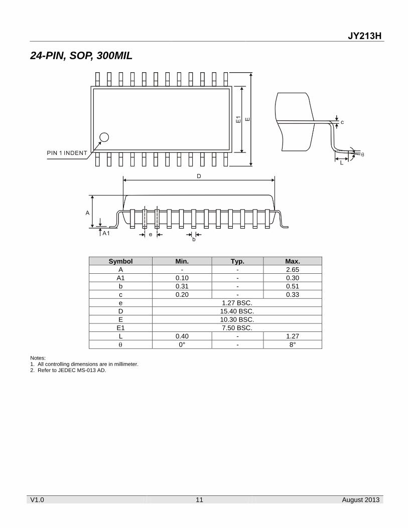
24-PIN, SOP, 300MIL
Symbol Min. Typ. Max.
A - - 2.65
A1 0.10 - 0.30
b 0.31 - 0.51
c 0.20 - 0.33
e 1.27 BSC.
D 15.40 BSC.
E 10.30 BSC.
E1 7.50 BSC.
L 0.40 - 1.27
0° - 8°
Notes: 1. All controlling dimensions are in millimeter.2. Refer to JEDEC MS-013 AD.

JY213H
V1.0 12 August 2013
28-PIN, SOP 300MIL
Symbol Min. Nom. Max.
A - - 2.65
A1 0.10 - 0.30
b 0.31 - 0.51
c 0.20 - 0.33
e 1.27BSC
D 17.90BSC
E 10.30BSC
E1 7.50BSC
L 0.38 - 1.27
θ 0° - 8°
Notes: 1. Controlling dimension is Millimeter.2. All dimensions refer to JEDEC standard MS-013 AE.