Embed Size (px)
Citation preview

Device Interface Board for Wireless LAN Testing
TeamMay 06-15
ClientECpE Department
Faculty AdvisorDr. Weber
Team MembersMatthew Dahms – EEJustine Skibbe – EEJoseph Chongo – EESrisarath Patneedi – CprE
December 06, 2005

Presentation Outline Project Overview
Introduction Problem Statement Assumptions and Limitations
System Considerations User Considerations
End-Product Description
Overview of Existing Work May 05-29 Team’s
Accomplishments Parallel-Serial Conversion Transmitters and Receivers FPGA
Project Activities Technology Considerations Present Accomplishments
Hardware Software
Planned Activities Design
Closure Materials Schedule Closing Summary
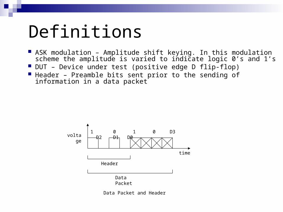
Definitions ASK modulation – Amplitude shift keying. In this modulation scheme the
amplitude is varied to indicate logic 0’s and 1’s DUT – Device under test (positive edge D flip-flop) Header – Preamble bits sent prior to the sending of information in a data packet
time
1 0 1 0 D3 D2 D1 D0
Data Packet
Header
voltage
Data Packet and Header

Definitions (cont.) NRZ – Non-return to zero. Using NRZ, a logic 1 bit is
sent as a high value and a logic 0 bit is sent as a low value.
PLL – Phase-locked loop RZ – Return to zero. This is the opposite of NRZ data.
The signal state is determined by the voltage during the first half of each data binary digit. The signal returns to a resting state (called zero) during the second half of each bit.

Project Overview

Acknowledgement
Dr. Weber Nathaniel Gibbs (GibbaHertz) Jason Boyd
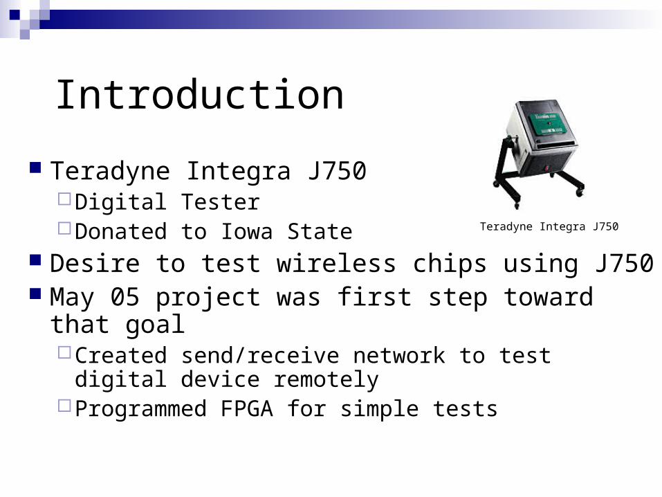
Introduction
Teradyne Integra J750Digital TesterDonated to Iowa State
Desire to test wireless chips using J750 May 05 project was first step toward that goal
Created send/receive network to test digital device remotely
Programmed FPGA for simple tests
Teradyne Integra J750

Project Overview Problem Statement
S/R network exists but no method is available for clock recovery
Must develop a clock recovering circuit and integrate it with current system
Investigate realistic range of operation for the wireless interface

Project Overview System Constraints
The Teradyne J750 must operate within +/- 3° C of calibrated temperature (30° C).
The maximum rate at which data may be sent is at 115.2 Kbps.
The Tx and Rx networks communicate at 916.5 & 916MHz. Nearby wireless signals at similar frequencies may disrupt the setup.
The IG-XL software shall be used in writing the test data sets for the Teradyne J750.
Only one FPGA will be provided.

Project Overview Users Assumptions
The user has knowledge in electrical and/or computer engineering.
The user has previous experience testing circuits with the Teradyne J750.
The user has read the Teradyne J750 instruction manual and will observe all necessary safety precautions as prescribed in that manual.
Intended Uses Functional test of a digital device (Future) Wireless chipset test
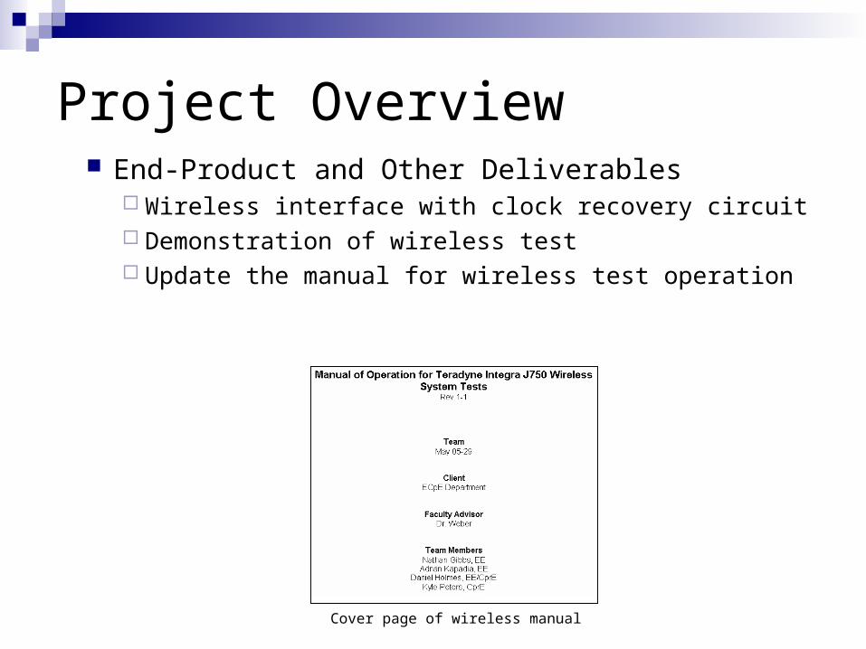
Project Overview End-Product and Other Deliverables
Wireless interface with clock recovery circuit Demonstration of wireless test Update the manual for wireless test operation
Cover page of wireless manual

Overview of Existing Work

Overview of Existing Work May 05-29 Accomplishments
Parallel-Serial Conversion Transmitters and Receivers Processing Device

Overview of Existing Work
Parallel-Serial Conversion Needed to convert parallel test data into serial test
data Chose to use a shift register
Shift Register attached to daughterboard

Overview of Existing Work
Transmitters and Receivers
TRM1
TRM2
RCV1
RCV2
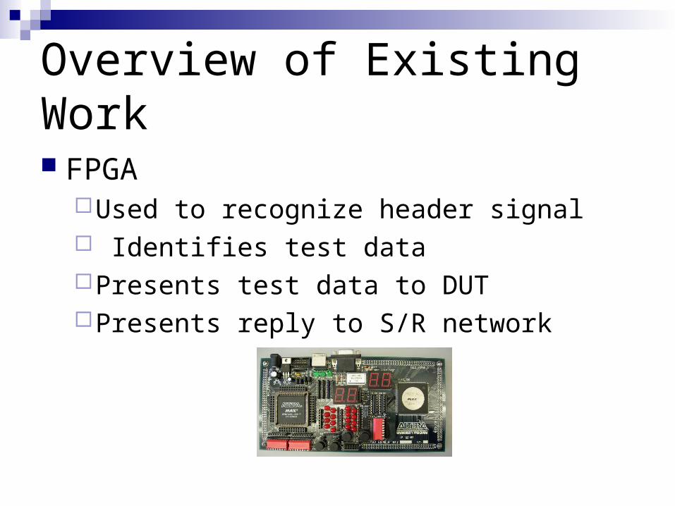
Overview of Existing Work
FPGAUsed to recognize header signal Identifies test dataPresents test data to DUTPresents reply to S/R network
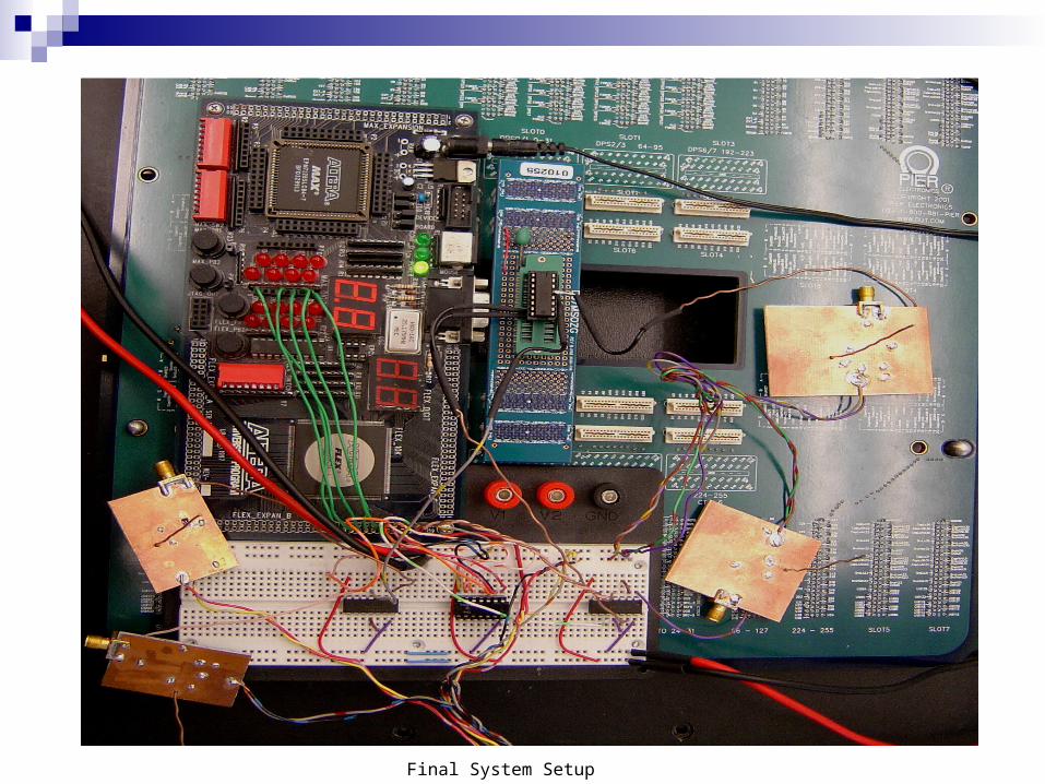
Final System Setup

Project Activities
Project Activities Project Definition
Part of the May 05 team’s project definition was to include a clock recovery circuit, but due to timing constraints was unable to do so.
May 06 goal is to integrate a PLL for clock recovery with the existing network.

Project Activities
Design
Project Activities
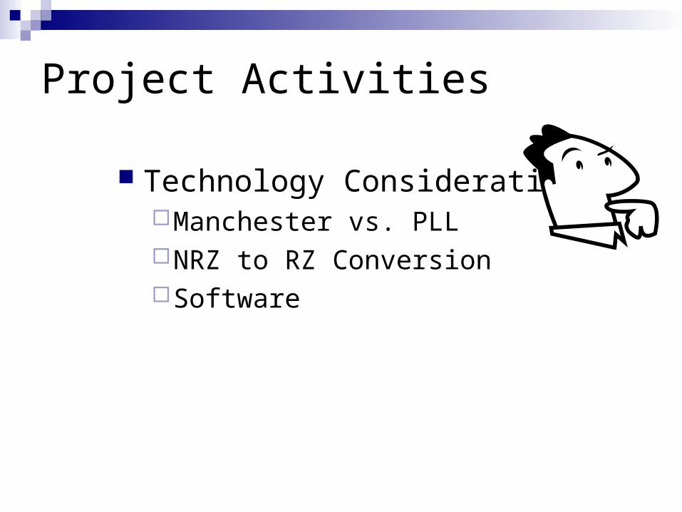
Technology ConsiderationsManchester vs. PLLNRZ to RZ ConversionSoftware

Project Activities
Original Signal Value SentLogic 0 0 to 1 (upward transition at
bit centre)
Logic 1 1 to 0 (downward transition at bit centre)
The waveform for a Manchester encoded bit stream carrying the sequence of bits 110100
Manchester Encoding
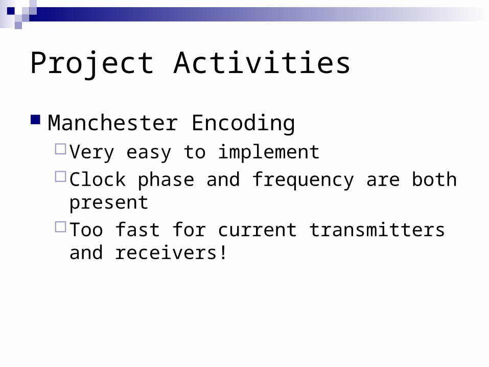
Manchester EncodingVery easy to implementClock phase and frequency are both present Too fast for current transmitters and
receivers!
Project Activities
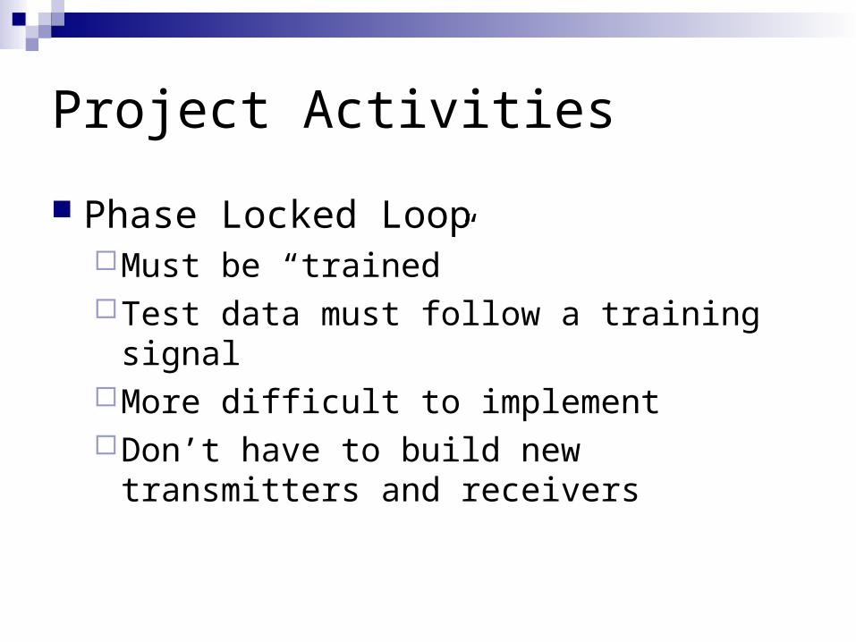
Project Activities
Phase Locked LoopMust be “trained” Test data must follow a training signalMore difficult to implementDon’t have to build new transmitters and
receivers

Project Activities
Present AccomplishmentsHardware
Previous team’s project setup and tested PLL Monostable Multivibrators
Software Prototype control software for FPGA written IG-XL test template written

Project Activities
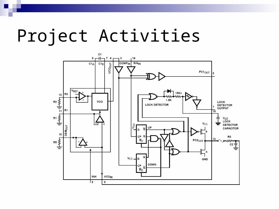
Internal Components of a PLL

Project Activities
Phase DetectorType I – XOR *Type II – Generates lead or lag pulses
Voltage Controlled Oscillator (VCO)Centered at 115.2 KHzFrequencies too far off of center frequency
will not lock
Project Activities
Project Activities
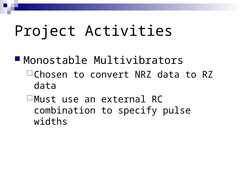
Monostable MultivibratorsChosen to convert NRZ data to RZ dataMust use an external RC combination to
specify pulse widths
Project Activities
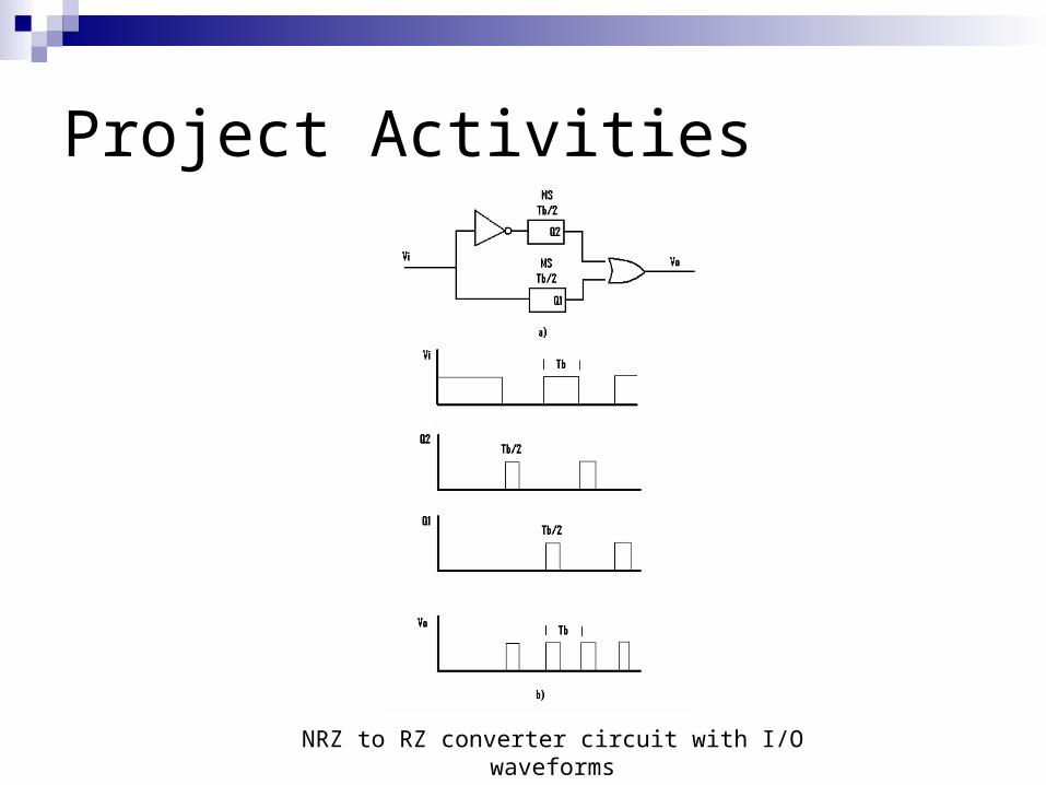
NRZ to RZ converter circuit with I/O waveforms

Project Activities
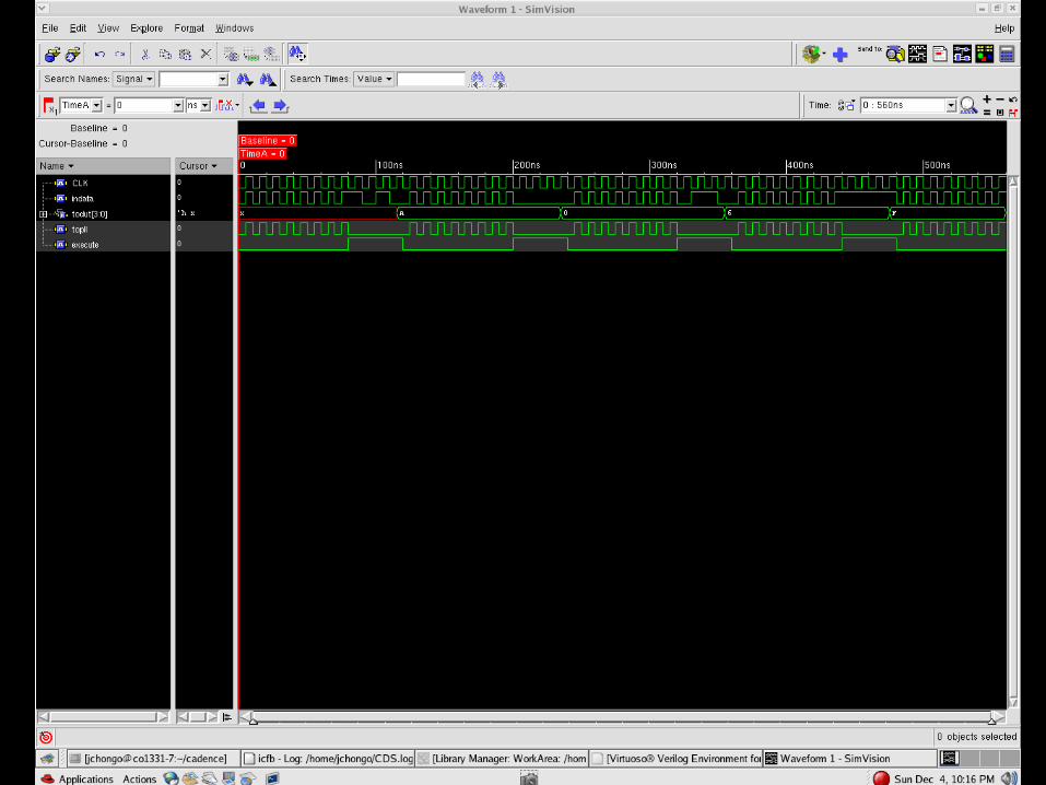
SoftwareFPGA serves as “brains” of systemVerilog chosen to program FPGAPrototype code complete
Project Activities


Project Activities Planned Design/Test Activities
Build and Test NRZ to RZ Converter Build and Test PLL Circuitry Integrate Clock Recovering Circuitry Modify FPGA Code as Necessary Test Functional Range of Wireless Interface

NRZ/RZ
PLL

Closure Materials

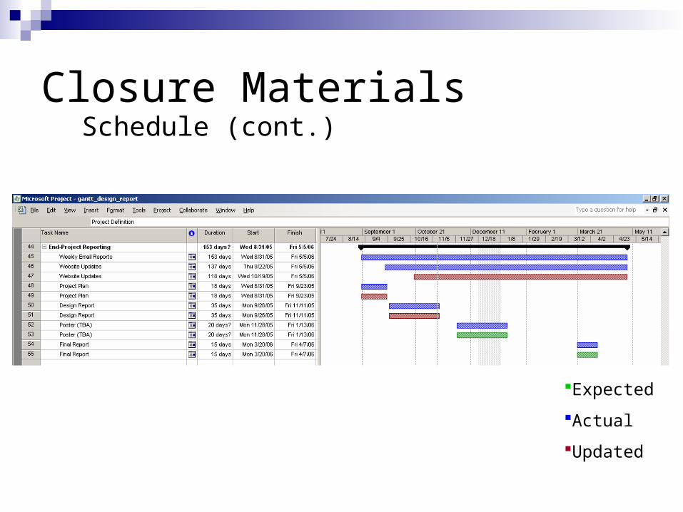
Closure MaterialsSchedule
Expected
Actual
Updated
Closure Materials
Expected
Actual
Updated
Schedule (cont.)
Closing Materials Lessons Learned
What technical knowledge was gained? FPGA implementation Teradyne Integra J750 usage Clock recovery methods System integration
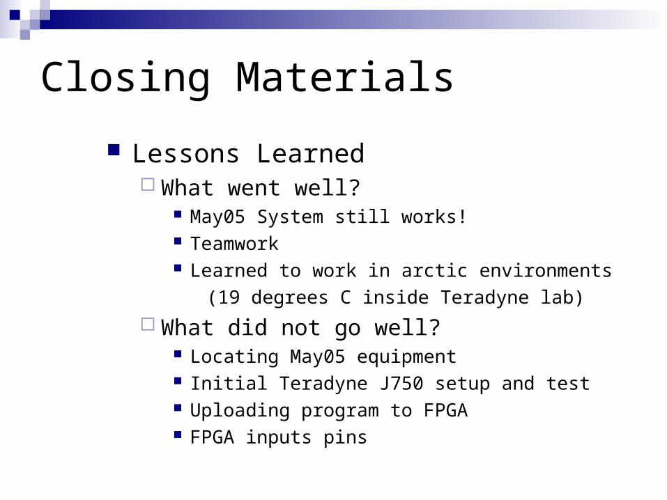
Closing Materials
Lessons Learned What went well?
May05 System still works! Teamwork Learned to work in arctic environments
(19 degrees C inside Teradyne lab)
What did not go well? Locating May05 equipment Initial Teradyne J750 setup and test Uploading program to FPGA FPGA inputs pins

Closing Materials Closing Summary
Problem – Integrate clock recovery circuitry into current system
Solution Use PLL for clock recovery Modify FPGA program to incorporate new
components

Questions?Questions???Questions???

Thank You