Embed Size (px)
Citation preview
Freescale SemiconductorErrata
© Freescale Semiconductor, Inc., 2009. All rights reserved.
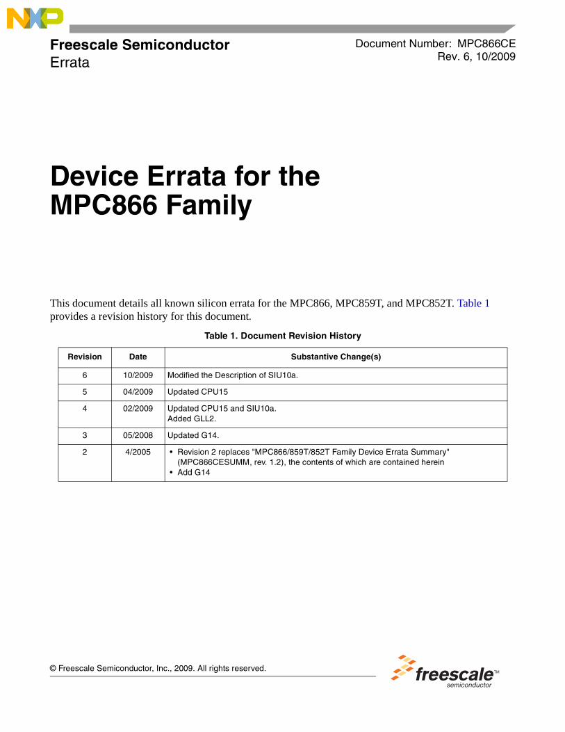
This document details all known silicon errata for the MPC866, MPC859T, and MPC852T. Table 1 provides a revision history for this document.
Table 1. Document Revision History
Revision Date Substantive Change(s)
6 10/2009 Modified the Description of SIU10a.
5 04/2009 Updated CPU15
4 02/2009 Updated CPU15 and SIU10a.Added GLL2.
3 05/2008 Updated G14.
2 4/2005 • Revision 2 replaces "MPC866/859T/852T Family Device Errata Summary" (MPC866CESUMM, rev. 1.2), the contents of which are contained herein
• Add G14
Document Number: MPC866CERev. 6, 10/2009
Device Errata for the MPC866 Family
Device Errata for the MPC866 Family , Rev. 6
2 Freescale Semiconductor
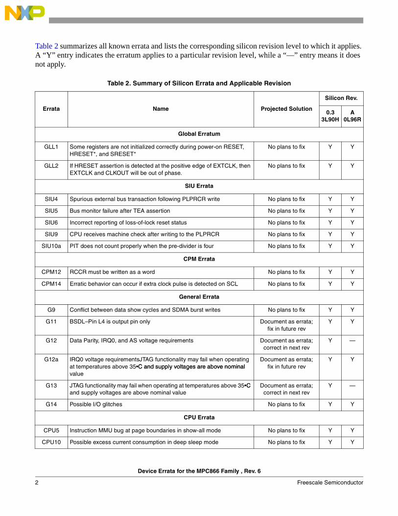
Table 2 summarizes all known errata and lists the corresponding silicon revision level to which it applies. A “Y” entry indicates the erratum applies to a particular revision level, while a “—” entry means it does not apply.
Table 2. Summary of Silicon Errata and Applicable Revision
Errata Name Projected Solution
Silicon Rev.
0.33L90H
A0L96R
Global Erratum
GLL1 Some registers are not initialized correctly during power-on RESET, HRESET*, and SRESET*
No plans to fix Y Y
GLL2 If HRESET assertion is detected at the positive edge of EXTCLK, then EXTCLK and CLKOUT will be out of phase.
No plans to fix Y Y
SIU Errata
SIU4 Spurious external bus transaction following PLPRCR write No plans to fix Y Y
SIU5 Bus monitor failure after TEA assertion No plans to fix Y Y
SIU6 Incorrect reporting of loss-of-lock reset status No plans to fix Y Y
SIU9 CPU receives machine check after writing to the PLPRCR No plans to fix Y Y
SIU10a PIT does not count properly when the pre-divider is four No plans to fix Y Y
CPM Errata
CPM12 RCCR must be written as a word No plans to fix Y Y
CPM14 Erratic behavior can occur if extra clock pulse is detected on SCL No plans to fix Y Y
General Errata
G9 Conflict between data show cycles and SDMA burst writes No plans to fix Y Y
G11 BSDL–Pin L4 is output pin only Document as errata;fix in future rev
Y Y
G12 Data Parity, IRQ0, and AS voltage requirements Document as errata;correct in next rev
Y —
G12a IRQ0 voltage requirementsJTAG functionality may fail when operating at temperatures above 35•C and supply voltages are above nominal C and supply voltages are above nominal value
Document as errata; fix in future rev
Y Y
G13 JTAG functionality may fail when operating at temperatures above 35•C C and supply voltages are above nominal value
Document as errata;correct in next rev
Y —
G14 Possible I/O glitches No plans to fix Y Y
CPU Errata
CPU5 Instruction MMU bug at page boundaries in show-all mode No plans to fix Y Y
CPU10 Possible excess current consumption in deep sleep mode No plans to fix Y Y
Device Errata for the MPC866 Family
Freescale Semiconductor 3
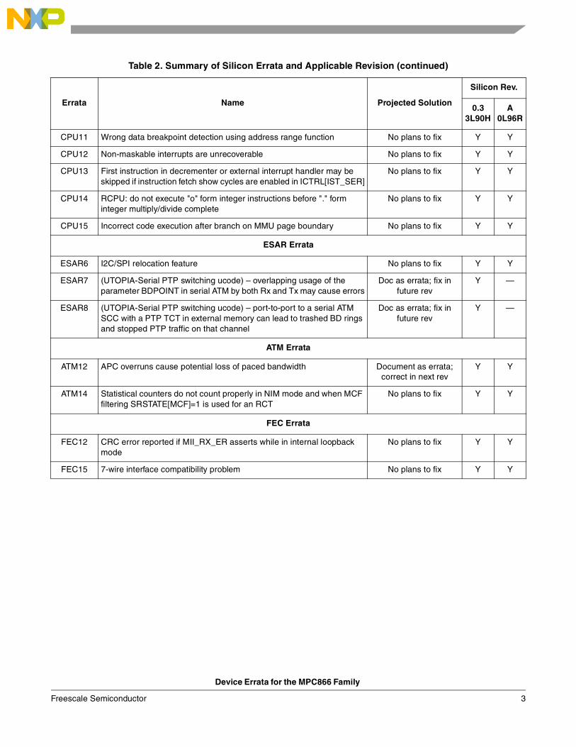
CPU11 Wrong data breakpoint detection using address range function No plans to fix Y Y
CPU12 Non-maskable interrupts are unrecoverable No plans to fix Y Y
CPU13 First instruction in decrementer or external interrupt handler may be skipped if instruction fetch show cycles are enabled in ICTRL[IST_SER]
No plans to fix Y Y
CPU14 RCPU: do not execute "o" form integer instructions before "." form integer multiply/divide complete
No plans to fix Y Y
CPU15 Incorrect code execution after branch on MMU page boundary No plans to fix Y Y
ESAR Errata
ESAR6 I2C/SPI relocation feature No plans to fix Y Y
ESAR7 (UTOPIA-Serial PTP switching ucode) – overlapping usage of the parameter BDPOINT in serial ATM by both Rx and Tx may cause errors
Doc as errata; fix in future rev
Y —
ESAR8 (UTOPIA-Serial PTP switching ucode) – port-to-port to a serial ATM SCC with a PTP TCT in external memory can lead to trashed BD rings and stopped PTP traffic on that channel
Doc as errata; fix in future rev
Y —
ATM Errata
ATM12 APC overruns cause potential loss of paced bandwidth Document as errata;correct in next rev
Y Y
ATM14 Statistical counters do not count properly in NIM mode and when MCF filtering SRSTATE[MCF]=1 is used for an RCT
No plans to fix Y Y
FEC Errata
FEC12 CRC error reported if MII_RX_ER asserts while in internal loopback mode
No plans to fix Y Y
FEC15 7-wire interface compatibility problem No plans to fix Y Y
Table 2. Summary of Silicon Errata and Applicable Revision (continued)
Errata Name Projected Solution
Silicon Rev.
0.33L90H
A0L96R
Device Errata for the MPC866 Family , Rev. 6
4 Freescale Semiconductor
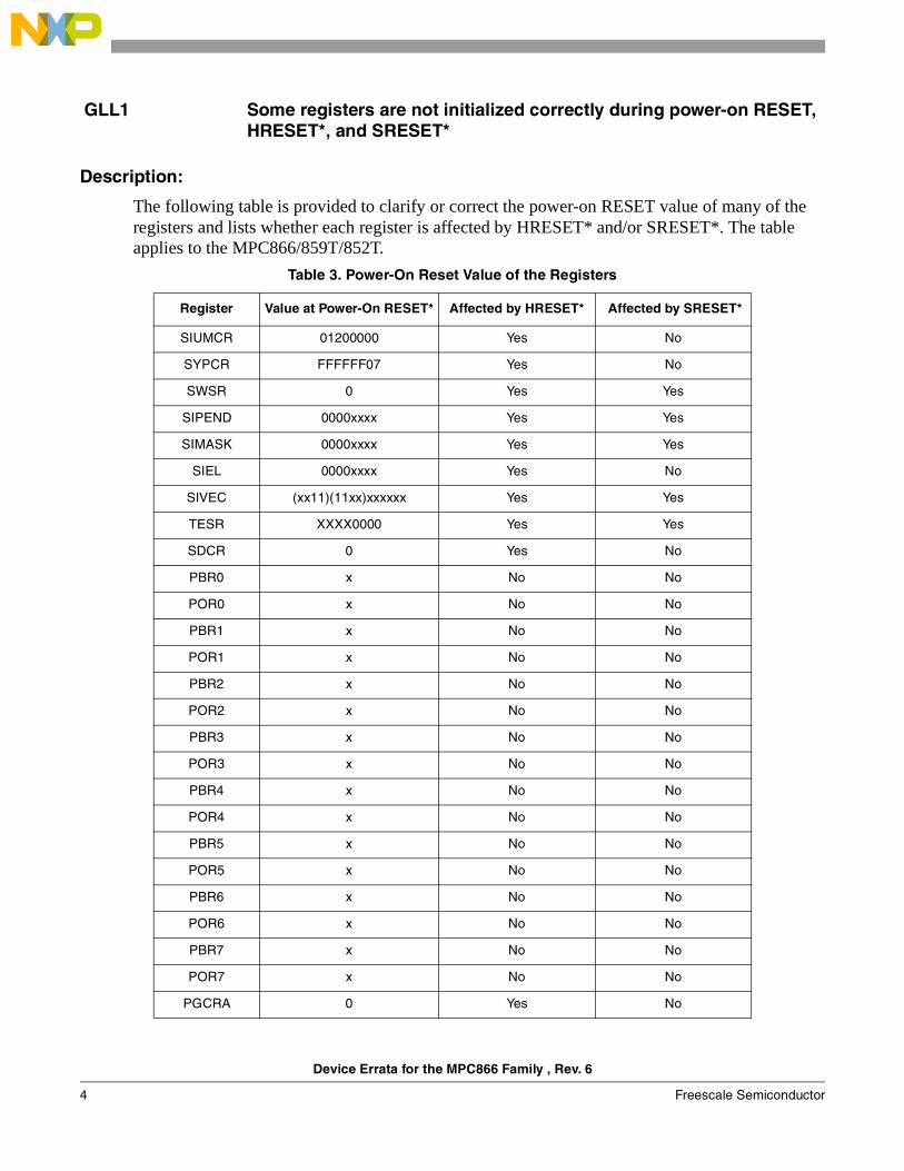
Description:
The following table is provided to clarify or correct the power-on RESET value of many of the registers and lists whether each register is affected by HRESET* and/or SRESET*. The table applies to the MPC866/859T/852T.
GLL1 Some registers are not initialized correctly during power-on RESET, HRESET*, and SRESET*
Table 3. Power-On Reset Value of the Registers
Register Value at Power-On RESET* Affected by HRESET* Affected by SRESET*
SIUMCR 01200000 Yes No
SYPCR FFFFFF07 Yes No
SWSR 0 Yes Yes
SIPEND 0000xxxx Yes Yes
SIMASK 0000xxxx Yes Yes
SIEL 0000xxxx Yes No
SIVEC (xx11)(11xx)xxxxxx Yes Yes
TESR XXXX0000 Yes Yes
SDCR 0 Yes No
PBR0 x No No
POR0 x No No
PBR1 x No No
POR1 x No No
PBR2 x No No
POR2 x No No
PBR3 x No No
POR3 x No No
PBR4 x No No
POR4 x No No
PBR5 x No No
POR5 x No No
PBR6 x No No
POR6 x No No
PBR7 x No No
POR7 x No No
PGCRA 0 Yes No
Device Errata for the MPC866 Family
Freescale Semiconductor 5
PGCRB 0 Yes No
PSCR x No No
PIPR ??00??00 Yes Yes
PER 0 Yes Yes
BR0 XXXXX(??00)0(000?) Yes No
OR0 00000FF4 Yes No
BR1 XXXXXX(xx00)0 Yes No
OR1 XXXXXXX(xxx0) Yes No
BR2 XXXXXX(xx00)0 Yes No
OR2 XXXXXXX(xxx0) Yes No
BR3 XXXXXX(xx00)0 Yes No
OR3 XXXXXXX(xxx0) Yes No
BR4 XXXXXX(xx00)0 Yes No
OR4 XXXXXXX(xxx0) Yes No
BR5 XXXXXX(xx00)0 Yes No
OR5 XXXXXXX(xxx0) Yes No
BR6 XXXXXX(xx00)0 Yes No
OR6 XXXXXXX(xxx0) Yes No
BR7 XXXXXX(xx00)0 Yes No
OR7 XXXXXXX(xxx0) Yes No
MAR x No No
MCR (xx00)0(x000)0(xxx0)X(00xx)X
Yes No
MAMR xx001000 Yes No
MBMR xx001000 Yes No
MSTAT 0 Yes No
MPTPR 0200 Yes No
MDR x No No
TBSCR 0 Yes No
TBREFA x No No
TBREFB x No No
RTCSC 00(000x)(000x) Yes Yes
RTC x No Yes
Table 3. Power-On Reset Value of the Registers (continued)
Register Value at Power-On RESET* Affected by HRESET* Affected by SRESET*
Device Errata for the MPC866 Family , Rev. 6
6 Freescale Semiconductor
RTSEC x No Yes
RTCAL x No No
PISCR 0 Yes No
PITC x No No
PITR x N/A N/A
SCCR 0(000?)(?000)(0??0)0000 Yes No
PLPRCR ???0(0100)000 Yes Yes
RSR 0 Yes Yes
TBSCRK x Yes Yes
TBREFAK x Yes Yes
TBREFBK x Yes Yes
TBK x Yes Yes
RTCSCK x Yes Yes
RTCK x Yes Yes
RTSECK x Yes Yes
RTCALK x Yes Yes
PISCRK x Yes Yes
PITCK x Yes Yes
SCCRK x Yes Yes
PLPRCRK x Yes Yes
RSRK x Yes Yes
I2MOD 0 Yes Yes
I2ADD x No No
I2BRG FFFF Yes No
I2COM 0 Yes Yes
I2CER 0 Yes Yes
I2CMR 0 Yes Yes
SDAR x No No
SDSR 0 Yes Yes
SDMR 0 Yes Yes
IDSR1 0 Yes Yes
IDMR1 0 Yes Yes
IDSR2 0 Yes Yes
Table 3. Power-On Reset Value of the Registers (continued)
Register Value at Power-On RESET* Affected by HRESET* Affected by SRESET*
Device Errata for the MPC866 Family
Freescale Semiconductor 7
IDMR2 0 Yes Yes
CIVR 0 Yes Yes
CICR 0 Yes No
CIPR 0 Yes Yes
CIMR 0 Yes Yes
CISR 0 Yes Yes
PADIR 0 Yes No
PAPAR 0 Yes No
PAODR 0 Yes No
PADAT x No No
PCDIR 0 Yes No
PCPAR 0 Yes No
PCSO 0 Yes No
PCDAT x No No
PCINT 0 Yes No
PDDIR 0 Yes No
PDPAR 0 Yes No
PDDAT x No No
TGCR 0 Yes Yes
TMR1 0 Yes Yes
TMR2 0 Yes Yes
TRR1 FFFF Yes Yes
TRR2 FFFF Yes Yes
TCR1 0 Yes Yes
TCR2 0 Yes Yes
TCN1 0 Yes Yes
TCN2 0 Yes Yes
TMR3 0 Yes Yes
TMR4 0 Yes Yes
TRR3 FFFF Yes Yes
TRR4 FFFF Yes Yes
TCR3 0 Yes Yes
TCR4 0 Yes Yes
Table 3. Power-On Reset Value of the Registers (continued)
Register Value at Power-On RESET* Affected by HRESET* Affected by SRESET*
Device Errata for the MPC866 Family , Rev. 6
8 Freescale Semiconductor
TCN3 0 Yes Yes
TCN4 0 Yes Yes
TER1 0 Yes Yes
TER2 0 Yes Yes
TER3 0 Yes Yes
TER4 0 Yes Yes
CPCR 0 Yes Yes
RCCR 0 Yes No
RCTR1 NA Yes Yes
RCTR2 NA Yes Yes
RCTR3 NA Yes Yes
RCTR4 NA Yes Yes
RTER 0 Yes Yes
RTMR 0 Yes Yes
BRGC1 0 Yes No
BRGC2 0 Yes No
BRGC3 0 Yes No
BRGC4 0 Yes No
GSMR_L1 0 Yes Yes
GSMR_H1 0 Yes Yes
PSMR1 0 Yes Yes
TODR1 0 Yes Yes
DSR1 7E7E Yes Yes
SCCE1 0 Yes Yes
SCCM1 0 Yes Yes
SCCS1 0 Yes Yes
GSMR_L2 0 Yes Yes
GSMR_H2 0 Yes Yes
PSMR2 0 Yes Yes
TODR2 0 Yes Yes
DSR2 7E7E Yes Yes
SCCE2 0 Yes Yes
SCCM2 0 Yes Yes
Table 3. Power-On Reset Value of the Registers (continued)
Register Value at Power-On RESET* Affected by HRESET* Affected by SRESET*
Device Errata for the MPC866 Family
Freescale Semiconductor 9
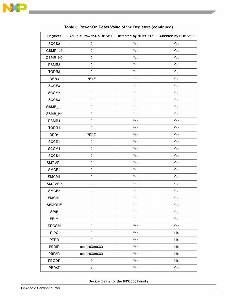
SCCS2 0 Yes Yes
GSMR_L3 0 Yes Yes
GSMR_H3 0 Yes Yes
PSMR3 0 Yes Yes
TODR3 0 Yes Yes
DSR3 7E7E Yes Yes
SCCE3 0 Yes Yes
SCCM3 0 Yes Yes
SCCS3 0 Yes Yes
GSMR_L4 0 Yes Yes
GSMR_H4 0 Yes Yes
PSMR4 0 Yes Yes
TODR4 0 Yes Yes
DSR4 7E7E Yes Yes
SCCE4 0 Yes Yes
SCCM4 0 Yes Yes
SCCS4 0 Yes Yes
SMCMR1 0 Yes Yes
SMCE1 0 Yes Yes
SMCM1 0 Yes Yes
SMCMR2 0 Yes Yes
SMCE2 0 Yes Yes
SMCM2 0 Yes Yes
SPMODE 0 Yes Yes
SPIE 0 Yes Yes
SPIM 0 Yes Yes
SPCOM 0 Yes Yes
PIPC 0 Yes No
PTPR 0 Yes No
PBDIR xxx(xx00)0000 Yes No
PBPAR xxx(xx00)0000 Yes No
PBODR 0 Yes No
PBDAT x Yes Yes
Table 3. Power-On Reset Value of the Registers (continued)
Register Value at Power-On RESET* Affected by HRESET* Affected by SRESET*
Device Errata for the MPC866 Family , Rev. 6
10 Freescale Semiconductor
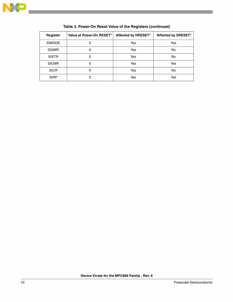
SIMODE 0 Yes Yes
SIGMR 0 Yes No
SISTR 0 Yes No
SICMR 0 Yes Yes
SICR 0 Yes No
SIRP 0 Yes Yes
Table 3. Power-On Reset Value of the Registers (continued)
Register Value at Power-On RESET* Affected by HRESET* Affected by SRESET*
Device Errata for the MPC866 Family
Freescale Semiconductor 11
Description:
In 1:2:1 mode, when HRESET is detected at the positive edge of EXTCLK, then there will be a loss of phase between EXTCLK and CLKOUT.
Projected Impact:
EXTCLK and CLKOUT will be out of phase.
Work Around:
EXTCLK and CLKOUT will come back in phase if either of the following programming sequences are followed:
• Reprogramming the PLPRCR:Program the PLPRCR such that the PLL clock will change, then reprogram the PLPRCR value back to the desired value.
OR
• Reprogram the SCCR:
1. Write 1'b00 to SCCR[EBDF].
2. Write 1'b01 to SCCR[EBDF].
3. Rewrite the desired value to the PLPRCR register.
Disposition:
Will not be fixed.
GLL2 If HRESET assertion is detected at the positive edge of EXTCLK, then EXTCLK and CLKOUT will be out of phase.
Device Errata for the MPC866 Family , Rev. 6
12 Freescale Semiconductor
Description:
This erratum affects only those designs that execute code from synchronous memories or bus slaves.
Spurious external bus transactions can occur after executing a store to the PLPRCR register, which changes the PLL multiplication factor (MF bits). This store causes the PLL to freeze the clocks while another external bus access is already visible on the pins of the chip. This appears externally as a transaction that begins, has its clocks frozen, and then is abruptly aborted without following the bus protocol.
This behavior affects only those systems with bus slaves that implement synchronous state machines that are sensitive to bus protocol violations. Synchronous DRAMs are not affected, and synchronous bus slaves that ignore bus signals when not selected (for example, the Tundra QSpan™ bus bridge) are not affected.
The only cases in which this erratum causes problems are the following:
— The device is executing code from a slave that implements a state machine dependent on the bus protocol, where that state machine might “get lost.”
— An external device snoops the PowerPC bus and implements a state machine; this state machine might “get lost.”
Projected Impact:
The impact of this erratum is minimal, and it will not be corrected.
Work Around:
The behavior exhibited in this erratum is a secondary symptom of the behavior of SIU9. See the description of SIU9 for the suggested workaround. The workaround also avoids the spurious external bus transaction that is described above.
SIU4 Spurious external bus transaction following PLPRCR write
Device Errata for the MPC866 Family
Freescale Semiconductor 13
Description:
The bus monitor does not activate for the access immediately following an access that terminated with a TEA assertion (either internally or externally generated). Therefore, if the following access is to an unmapped address, the MPC866/859T/852T does not terminate access. If this situation is allowed to occur, this cycle could potentially be endless and cause the system to hang.
Projected Impact:
The impact of this erratum is minimal, and it will not be corrected.
Work Around:
Either of the following serves as a workaround for this erratum:
— Avoid this situation (which should not occur in a normal system)
— Terminate the cycle externally (for example, implement an external bus monitor)
— Rely on the software watchdog timer to reset the system if this error occurs
SIU5 Bus monitor failure after TEA assertion
Device Errata for the MPC866 Family , Rev. 6
14 Freescale Semiconductor
Description:
The RSR[LLRS] bit is set by both unintentional and software-initiated loss-of-lock. The RSR[LLRS] bit should be set only by an unintentional loss-of-lock. Software-initiated loss-of-lock (for example, changing the SPLL multiplication factor or entering low-power modes) should not set this bit.
Projected Impact:
The impact of this erratum is minimal, and it will not be corrected.
Work Around:
The PLPRCR[SPLSS] functions as intended. Reference this bit instead.
SIU6 Incorrect reporting of loss-of-lock reset status
Device Errata for the MPC866 Family
Freescale Semiconductor 15
Description:
The CPU may receive a machine check after writing to the PLPRCR. An extra clock that the clock block generates after the SIU releases the bus causes this error.
The error occurs when the CPU begins a transaction after the SIU releases the internal bus. The PLPRCR write causes the CPU’s clocks to stop. However, the extra clock allows the CPU’s transaction to begin before the clocks stop. Therefore, the CPU’s clocks are stopped in mid-transaction, and its transaction never receives an acknowledgement. When the CPU resumes operation, it receives a machine check.
The failure mechanism is due to an internal logic synchronization issue aggravated by memory refreshes performed by the UPM. The problem is most often exhibited when entering and exiting low-power modes frequently, such as when using doze mode to conserve power. The probability of encountering this problem is small but finite (approximately one in a million).
Work Around:
Prevent the CPU from getting the bus during the extra clock following the PLPRCR write. Enable the instruction cache and create a software delay. To calculate the delay length, take the longest bus transaction in CPU clocks (including memory refresh or PCMCIA access). The resultant number of clocks must be executed using instructions such as NOP (1 clock), ISYNC (2 clocks) or DIVW (13 clocks). The instructions for the delay must either fit in one cache line, or some other mechanism must be used to make certain that the instructions for the delay are in cache. The instructions of the delay must be executed after the PLPRCR write, which can be enforced by the ISYNC instruction. The length of the software delay must also be greater than or equal to the length of the longest bus transaction (in CPU clocks).
For example, if your longest transaction is 8 bus clocks and the CPU is in 1:2 mode, the delay required is 16 clocks. This requirement can be accomplished with two DIVW instructions. The instruction cache must be enabled to make certain that the code sequence is loaded into the cache as a unit, and the PLPRCR write should be aligned to a 16-byte boundary to ensure it is the first instruction in the cache line containing the sequence.
Freescale suggests the following workaround software:
.align 16
.global SetPLPRCR
SetPLPRCR:
stw 4, PLPRCR_OFFSET(3) # burst aligned address
isync # isync
addi 3, 0, 1 # safeguard against divide-by-zero
divw 4, 4, 3
divw 4, 4, 3
blr
SIU9 CPU receives machine check after writing to the PLPRCR
Device Errata for the MPC866 Family , Rev. 6
16 Freescale Semiconductor
Description:
The periodic interrupt timer (PIT) consists of a 16-bit counter clocked by the PITRCLK clock supplied by the clock module.
The user can program the RTC and PIT clock to be divided by 4 or 512 (depending on SCCR[RTDIV]).
Due to a race condition generating a timing violation, the periodic interrupt timer (PIT) does not count properly when the predivider in SCCR[PTDIV] is four.
This situation may also affect the generation of interrupts from the PIT.
Work Around:
Use a pre-divider of 512 setting SCCR[PTDIV] = 1.
SIU10a PIT does not count properly when the pre-divider is four
Device Errata for the MPC866 Family
Freescale Semiconductor 17
Description:
If the RCCR is written as a byte or half word (to addresses IMMR+0x9C4, IMMR+0x9C5), RCCR[ERAM4K] (located at address IMMR+0x9C7) is cleared.
Work Around:
To change the RCCR bytes at address IMMR+(0x9c4/0x9c5), write the whole word.
CPM12 RCCR must be written as a word
Device Errata for the MPC866 Family , Rev. 6
18 Freescale Semiconductor
Description:
The I2C controller has an internal counter that counts the number of bits sent. This counter is reset when the I2C controller detects a START condition. When an extra SCL clock pulse is inserted in between transactions (before START and after STOP conditions), the internal counter may not be reset correctly, which could generate partial frames (less than eight bits) in the next transaction.
Work Around:
Do not generate SCL pulses in between transactions. In a noisy environment the digital filter I2MOD[FLT] and additional filtering capacitors should be used on SCL to eliminate clock spikes that may be misinterpreted as clock pulses.
CPM14 Erratic behavior can occur if extra clock pulse is detected on SCL
Device Errata for the MPC866 Family
Freescale Semiconductor 19
Description:
If data show cycles are enabled via SIUMCR[DSHW]
AND an internal register or dual-port RAM access is made immediately following an SDMA burst write,
THEN the SDMA burst write may be corrupted. The observed phenomenon is that a burst write with four operands holds the second operand into the third and fourth burst beats. For example, a burst write of A-B-C-D will be observed on the bus as A-B-B-B.
Note: This behavior can also occur when the SDMA burst is to burst-inhibited memory. Setting the memory to burst-inhibited does not solve the problem.
Work Around:
Do not use data show cycles in a system that performs SDMA bursts. These include systems that use ATM, fast Ethernet, and memory-to-memory IDMA.
G9 Conflict between data show cycles and SDMA burst writes
Device Errata for the MPC866 Family , Rev. 6
20 Freescale Semiconductor
Description:
This pin can be used only in output mode during JTAG scan testing.
Work Around:
No work around is available.
G11 BSDL–Pin L4 is output pin only
Device Errata for the MPC866 Family
Freescale Semiconductor 21
Description:
The following pins require voltage relaxation to guaranty proper operation for the MPC866/859T/852T:
Data parity (DP0, DP1, DP2, and DP3) pins require a lower than nominal vil level.
IRQ0 requires a higher than nominal vih level.
AS requires a higher than nominal vih level.
Work Around:
Vil for data parity pins should be < 0.6 V.
VIh for IRQ0 pin should be > 2.2 V.
VIh for AS pin should be > 2.2 V.
G12 Data Parity, IRQ0, and AS voltage requirements
Device Errata for the MPC866 Family , Rev. 6
22 Freescale Semiconductor
Description:
The IRQ0 pin requires voltage a higher than nominal vih level to guarantee proper operation for the MPC866/859T/852T.
Work Around:
VIh for IRQ0 pin should be > 2.2 V.
G12a IRQ0 voltage requirements
Device Errata for the MPC866 Family
Freescale Semiconductor 23
Work Around:
Perform boundary scan testing at temperature less than or equal to 35 C and apply VDDL voltage less than or equal to 1.83V.
G13 JTAG functionality may fail when operating at temperatures above 35•C and supply voltages are above nominal valueC and supply voltages are above nominal value
Device Errata for the MPC866 Family , Rev. 6
24 Freescale Semiconductor
Description:
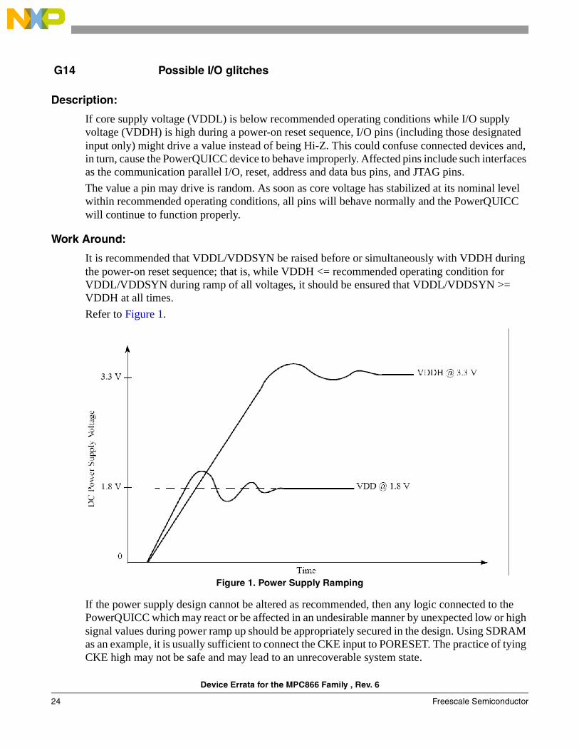
If core supply voltage (VDDL) is below recommended operating conditions while I/O supply voltage (VDDH) is high during a power-on reset sequence, I/O pins (including those designated input only) might drive a value instead of being Hi-Z. This could confuse connected devices and, in turn, cause the PowerQUICC device to behave improperly. Affected pins include such interfaces as the communication parallel I/O, reset, address and data bus pins, and JTAG pins.
The value a pin may drive is random. As soon as core voltage has stabilized at its nominal level within recommended operating conditions, all pins will behave normally and the PowerQUICC will continue to function properly.
Work Around:
It is recommended that VDDL/VDDSYN be raised before or simultaneously with VDDH during the power-on reset sequence; that is, while VDDH <= recommended operating condition for VDDL/VDDSYN during ramp of all voltages, it should be ensured that VDDL/VDDSYN >= VDDH at all times.
Refer to Figure 1.
Figure 1. Power Supply Ramping
If the power supply design cannot be altered as recommended, then any logic connected to the PowerQUICC which may react or be affected in an undesirable manner by unexpected low or high signal values during power ramp up should be appropriately secured in the design. Using SDRAM as an example, it is usually sufficient to connect the CKE input to PORESET. The practice of tying CKE high may not be safe and may lead to an unrecoverable system state.
G14 Possible I/O glitches
Device Errata for the MPC866 Family
Freescale Semiconductor 25
Description:
The wrong instruction address is driven by the core when all the following conditions occur:
MPC866/859T/852T works in 'show all' mode (for example, ISCT_SER bits=000 in ICTRL).
— Sequential instruction crosses IMMU page boundary.
— Instruction cache fails to get ownership of the internal U-bus on the first clock.
In this case, the address that the core drives is of the previous page rather than the current one.
The impact of this erratum is minimal, and will not be corrected.
Work Around:
Either of the following can serve as a workaround to this erratum:
— Disable show all mode.
— Invalidate the page next to current (by using the tlbie instruction) when performing the TLB reload operation.
CPU5 Instruction MMU bug at page boundaries in show-all mode
Device Errata for the MPC866 Family , Rev. 6
26 Freescale Semiconductor
Description:
Certain nodes of the multiplier hardware are not initialized at reset, and may cause non-destructive internal contention. As a result, if the processor is put into Deep Sleep mode without first putting the multiplier into a known state, current consumption in this mode may be higher than expected.
Projected Impact:
The impact of this erratum is minimal, and it will not be corrected.
Work Around:
Execute a mullw instruction at any point after reset to put the internal nodes in an orderly state. Deep Sleep mode may then be entered at any time thereafter.
CPU10 Possible excess current consumption in deep sleep mode
Device Errata for the MPC866 Family
Freescale Semiconductor 27
Description:
When the data breakpoint/watchpoint logic is used to trap on load/store accesses to addresses less than or greater than a given address, erroneous detection can occur. This error occurs for byte-size load/stores where the address accessed and the compare address (in comparator E or F) differ only in the two least-significant bits and the two least-significant bits of the address accessed are not 00.
Projected Impact:
The impact of this erratum is minimal, and it will not be corrected.
Work Around:
Select the address in the compare register (E or F) so that it differs by more than the two least-significant bits from the address range to be detected. For example, if the address range that you want to detect are addresses less than or equal to 0xA0000006, then use address 0xA0000008 instead.
CPU11 Wrong data breakpoint detection using address range function
Device Errata for the MPC866 Family , Rev. 6
28 Freescale Semiconductor
Description:
When an interrupt occurs during an RFI instruction, the RFI partially executes before the exception is taken. The ‘partial execution’ includes copying the contents of SRR1 to the MSR. Therefore, the MSR value seen in the exception handler is the MSR value of the previous machine state, not of the machine state when the RFI occurred. The contents of the MSR is therefore unreliable upon entry into this ‘second’ exception routine.
Work Around:
This erratum only affects exceptions that can occur during an RFI instruction. For a normal application, the only exceptions that can occur during an RFI instruction are non-maskable interrupts or breakpoints. [External interrupts are masked during the machine-state recovery portion of an exception handler.] Therefore, workarounds for only these two cases are required:
Do not put an instruction breakpoint on an RFI instruction.
Because the state of the MSR[RI] bit is not reliable, treat all non-maskable interrupts as non-recoverable.
CPU12 Non-maskable interrupts are unrecoverable
Device Errata for the MPC866 Family
Freescale Semiconductor 29
Background:
The MPC866/859T/852T IMMU works in the following way: Each time there is an access from the core, the access reaches the cache using the page from the previous access, on the assumption that the page has not changed. Usually that assumption is correct and no stall occurs. If the page has changed, a retry is done with the correct page. The MMU also signals the cache to disregard the previous access since the page was incorrect and the results are useless. When a TLB miss occurs, there is no retry, but the previous access is normally aborted since it used the wrong page value. Then the MMU shuts itself off until there is an abort signal from the core that specifies a change in flow. Normally, this change of flow is the ITLB miss exception, in which case the instruction pipeline is cleared before taking the exception. However, if the decrementer or external interrupt is asserted, this exception can take precedence over the ITLB miss exception.
Description:
An ITLB miss followed immediately by a decrementer or external interrupt exception was detected. The first address of the exception routine is then presented by the core. Because the previous page was not valid (ITLB miss), the MMU provides an incorrect address (ff800500). As a result of the internal state of the MMU and the fact that it is a program trace show cycle, this cycle is (mistakenly) not cancelled, although it is re-tried, causing the bad address to appear on the external bus as a show cycle. Although the show cycle is incorrect, the program flow usually continues correctly.
However, if the internal U-Bus pipeline happens to be full on the cycle discussed above, the retry is not handled correctly (as a result of the same issue mentioned above) and the second address of the routine (504) is used for the fetch instead of the first address (500), causing the instructions of the first cache line to be fetched in the wrong order.
Work Around:
1. Because the first instruction of the decrementer and external interrupt routines might not be executed before the second instruction, it should not do anything useful, so it won't matter if it is skipped. Therefore, a nop or isync instruction should be placed in this location. An isync instruction should be placed in the second location of these routines to re-synchronize the core with the IMMU. If the bug occurs, the isync instruction at 504 is executed as if it is at location 500, and causes another fetch of itself from address 504. At this point, the program flow is re-synchronized and continues as usual.
2. Disable instruction fetch show cycle in ICTRL[IST_SER].
CPU13 First instruction in decrementer or external interrupt handler may be skipped if instruction fetch show cycles are enabled in ICTRL[IST_SER]
Device Errata for the MPC866 Family , Rev. 6
30 Freescale Semiconductor
Description:
When "o" form integer instruction is started to execute before previously started "." form integer multiply or divide instruction completes, the Condition Register bit #3 (SO) may be incorrectly updated by XER[SO] bit changed by "o" form instruction. For example, instruction sequence "divw. Rz,Rx,Ry, subfo Rt,Rv,Ru" may cause this problem. It does not happen if the "o" form instruction is also "." form or register dependencies exist.
Work Around:
Any of the following can serve as a workaround for this erratum:
1. Keep the "o" form instruction 4 integer or 6 other instructions apart from integer divide "." form instruction in the code or more than 1 instruction in case of integer multiply instruction.
2. Use both instructions with the "." form.
3. Run RCPU in serialized mode.
4. Place the "sync" instruction between multiply/divide and "o" form integer instruction.
5. Don't use "." form of integer divide or multiply instructions. CPU14. RCPU: do not execute "o" form integer instructions before "." form integer multiply/divide complete.
CPU14 RCPU: do not execute "o" form integer instructions before "." form integer multiply/divide complete
Device Errata for the MPC866 Family
Freescale Semiconductor 31
CPU15 Incorrect code execution after branch on MMU page boundaryDescription:
An incorrect or invalid instruction is executed if all of the following are true:
• A conditional branch or branch to LR/CTR is executed in the last word of MMU page <n> (branches with primary opcodes 16 or 19).
• The target address of the branch points to the last cache line of MMU page <n>+1.
• The branch remains unresolved long enough for a prefetch of the first cache line of MMU page <n>+1 to start.
• Code execution continues after the branch beyond the end of MMU page <n>+1 into the first cache line of page <n>+2, which must already be in the cache.
• Both ICACHE and IMMU are enabled.
An incorrect or invalid instruction will be executed instead of the correct one out of the first cache line of MMU page <n>+2.
NOTEAbsolute branches (bx with primary opcode 18) are not the cause of the problem, as they are always resolved implicitly. Every MMU page containing a “risky” branch as described above is called a “risky” page below.
CPU15 Incorrect code execution after branch on MMU page boundary
Device Errata for the MPC866 Family , Rev. 6
32 Freescale Semiconductor
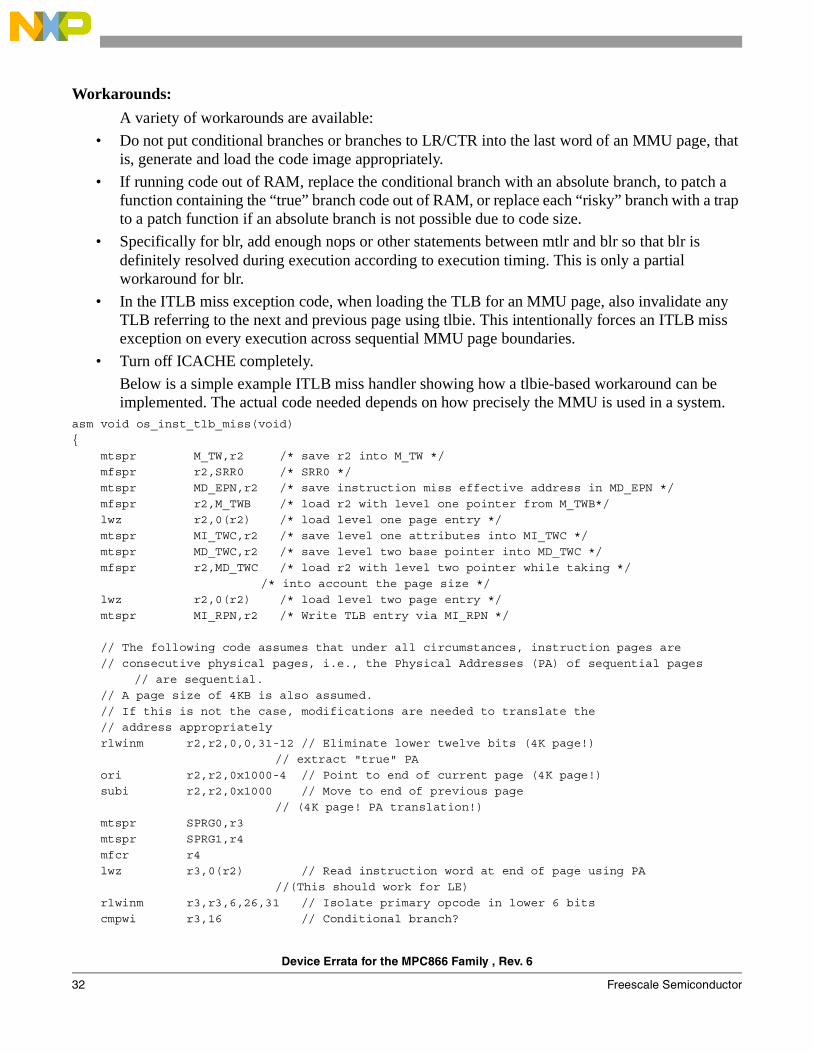
Workarounds:
A variety of workarounds are available:
• Do not put conditional branches or branches to LR/CTR into the last word of an MMU page, that is, generate and load the code image appropriately.
• If running code out of RAM, replace the conditional branch with an absolute branch, to patch a function containing the “true” branch code out of RAM, or replace each “risky” branch with a trap to a patch function if an absolute branch is not possible due to code size.
• Specifically for blr, add enough nops or other statements between mtlr and blr so that blr is definitely resolved during execution according to execution timing. This is only a partial workaround for blr.
• In the ITLB miss exception code, when loading the TLB for an MMU page, also invalidate any TLB referring to the next and previous page using tlbie. This intentionally forces an ITLB miss exception on every execution across sequential MMU page boundaries.
• Turn off ICACHE completely.
Below is a simple example ITLB miss handler showing how a tlbie-based workaround can be implemented. The actual code needed depends on how precisely the MMU is used in a system.
asm void os_inst_tlb_miss(void)
{
mtspr M_TW,r2 /* save r2 into M_TW */
mfspr r2,SRR0 /* SRR0 */
mtspr MD_EPN,r2 /* save instruction miss effective address in MD_EPN */
mfspr r2,M_TWB /* load r2 with level one pointer from M_TWB*/
lwz r2,0(r2) /* load level one page entry */
mtspr MI_TWC,r2 /* save level one attributes into MI_TWC */
mtspr MD_TWC,r2 /* save level two base pointer into MD_TWC */
mfspr r2,MD_TWC /* load r2 with level two pointer while taking */
/* into account the page size */
lwz r2,0(r2) /* load level two page entry */
mtspr MI_RPN,r2 /* Write TLB entry via MI_RPN */
// The following code assumes that under all circumstances, instruction pages are
// consecutive physical pages, i.e., the Physical Addresses (PA) of sequential pages
// are sequential.
// A page size of 4KB is also assumed.
// If this is not the case, modifications are needed to translate the
// address appropriately
rlwinm r2,r2,0,0,31-12 // Eliminate lower twelve bits (4K page!)
// extract "true" PA
ori r2,r2,0x1000-4 // Point to end of current page (4K page!)
subi r2,r2,0x1000 // Move to end of previous page
// (4K page! PA translation!)
mtspr SPRG0,r3
mtspr SPRG1,r4
mfcr r4
lwz r3,0(r2) // Read instruction word at end of page using PA
//(This should work for LE)
rlwinm r3,r3,6,26,31 // Isolate primary opcode in lower 6 bits
cmpwi r3,16 // Conditional branch?
Device Errata for the MPC866 Family
Freescale Semiconductor 33
beq @tlbieprev // Invalidate previous page
cmpwi r3,19 // Possibly conditional branch to register address?
beq @tlbieprev // Invalidate previous page
addi r2,r2,0x1000 // Move back to current page address
// (4K page! PA translation!)
lwz r3,0(r2) // Read instruction word at end of page using PA
//(This should work for LE)
rlwinm r3,r3,6,26,31 // Isolate primary opcode in lower 6 bits
cmpwi r3,16 // Conditional branch?
beq @tlbienext // Invalidate next page
cmpwi r3,19 // Possibly conditional branch to register address?
beq @tlbienext // Invalidate next page
mtcr r4
mfspr r4,SPRG1
mfspr r3,SPRG0
mfspr r2,M_TW /* Restore r2 previously saved in M_TW */
rfi
@tlbienext:
addi r2,r2,0x1000 // Move to next page address (4K page! PA translation!)
@tlbieprev:
tlbie r2 // Make sure we refetch the ITLB on the dangerous page
mtcr r4
mfspr r4,SPRG1
mfspr r3,SPRG0
mfspr r2,M_TW /* Restore r2 previously saved in M_TW */
rfi
} /* os_inst_tlb_miss */
A variant that is further optimized can often be generated to avoid memory reloads. However, this specifically depends on MMU usage in the system. The following example handler improves performance by relying on three bits of a L2 TLB part not being used by other software.
asm void os_inst_tlb_miss_l2_based(void)
{
mtspr SPRG0,r3
mtspr SPRG1,r4
mfcr r4
mtspr M_TW,r2 /* save r2 into M_TW */
mfspr r2,SRR0 /* SRR0 */
mtspr MD_EPN,r2 /* save instruction miss effective address in MD_EPN */
mfspr r2,M_TWB /* load r2 with level one pointer from M_TWB*/
lwz r2,0(r2) /* load level one page entry */
mtspr MI_TWC,r2 /* save level one attributes into MI_TWC */
mtspr MD_TWC,r2 /* save level two base pointer into MD_TWC */
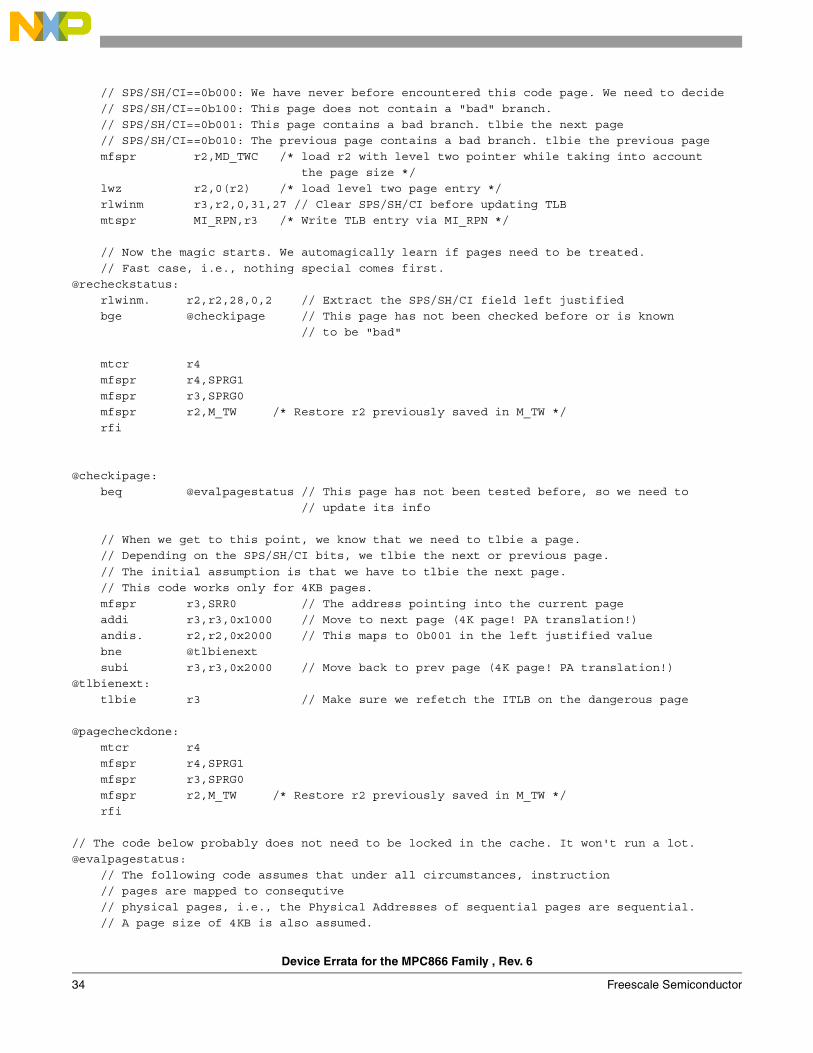
// We abuse the SPS/SH/CI bits as indicator of our state in terms of the erratum.
// We know that they are normally 0 in most applications, which is why we chose them.
Device Errata for the MPC866 Family , Rev. 6
34 Freescale Semiconductor
// SPS/SH/CI==0b000: We have never before encountered this code page. We need to decide
// SPS/SH/CI==0b100: This page does not contain a "bad" branch.
// SPS/SH/CI==0b001: This page contains a bad branch. tlbie the next page
// SPS/SH/CI==0b010: The previous page contains a bad branch. tlbie the previous page
mfspr r2,MD_TWC /* load r2 with level two pointer while taking into account
the page size */
lwz r2,0(r2) /* load level two page entry */
rlwinm r3,r2,0,31,27 // Clear SPS/SH/CI before updating TLB
mtspr MI_RPN,r3 /* Write TLB entry via MI_RPN */
// Now the magic starts. We automagically learn if pages need to be treated.
// Fast case, i.e., nothing special comes first.
@recheckstatus:
rlwinm. r2,r2,28,0,2 // Extract the SPS/SH/CI field left justified
bge @checkipage // This page has not been checked before or is known
// to be "bad"
mtcr r4
mfspr r4,SPRG1
mfspr r3,SPRG0
mfspr r2,M_TW /* Restore r2 previously saved in M_TW */
rfi
@checkipage:
beq @evalpagestatus // This page has not been tested before, so we need to
// update its info
// When we get to this point, we know that we need to tlbie a page.
// Depending on the SPS/SH/CI bits, we tlbie the next or previous page.
// The initial assumption is that we have to tlbie the next page.
// This code works only for 4KB pages.
mfspr r3,SRR0 // The address pointing into the current page
addi r3,r3,0x1000 // Move to next page (4K page! PA translation!)
andis. r2,r2,0x2000 // This maps to 0b001 in the left justified value
bne @tlbienext
subi r3,r3,0x2000 // Move back to prev page (4K page! PA translation!)
@tlbienext:
tlbie r3 // Make sure we refetch the ITLB on the dangerous page
@pagecheckdone:
mtcr r4
mfspr r4,SPRG1
mfspr r3,SPRG0
mfspr r2,M_TW /* Restore r2 previously saved in M_TW */
rfi
// The code below probably does not need to be locked in the cache. It won't run a lot.
@evalpagestatus:
// The following code assumes that under all circumstances, instruction
// pages are mapped to consequtive
// physical pages, i.e., the Physical Addresses of sequential pages are sequential.
// A page size of 4KB is also assumed.
Device Errata for the MPC866 Family
Freescale Semiconductor 35
// If this is not the case, modifications are needed to translate the address
// appropriately
rlwinm r2,r3,0,0,31-12 // Eliminate lower twelve bits (4K page!) to extract
// "true" PA
ori r2,r2,0x1000-4 // Point to end of current page (4K page!)
lwz r3,0(r2) // Read instruction word at end of page using PA
// (This should work for LE)
rlwinm r3,r3,6,26,31 // Isolate primary opcode in lower 6 bits
cmpwi r3,16 // Conditional branch?
beq @riskypage // This is a risky page
cmpwi r3,19 // Possibly conditional branch to register address?
beq @riskypage // This is a risky page
subi r2,r2,0x1000 // Move to the previous page (4K page! PA translation!)
lwz r3,0(r2) // Read instruction word at end of page using PA
// (This should work for LE)
rlwinm r3,r3,6,26,31 // Isolate primary opcode in lower 6 bits
cmpwi r3,16 // Conditional branch?
beq @prevrisky // We are on the page after a risky one
cmpwi r3,19 // Possibly conditional branch to register address?
beq @prevrisky // We are on the page after a risky one
// This page is not risky and not near a risky page. So we mark it as safe!
mfspr r3,MD_TWC /* load r3 with level two pointer while taking into account
the page size */
lwz r2,0(r3) /* load level one page entry */
ori r2,r2,0x0008 // Set SPS/SH/CI to 0b100 for an innocent page
stw r2,0(r3) /* store level one page entry */
b @pagecheckdone
@prevrisky:
mfspr r3,MD_TWC /* load r3 with level two pointer while taking into account
the page size */
lwz r2,0(r3) /* load level one page entry */
ori r2,r2,0x0004 // Set SPS/SH/CI to 0b010 for a page next to a risky one
stw r2,0(r3) /* store level one page entry */
b @recheckstatus
@riskypage:
mfspr r3,MD_TWC /* load r3 with level two pointer while taking into account
the page size */
lwz r2,0(r3) /* load level one page entry */
ori r2,r2,0x0002 // Set SPS/SH/CI to 0b001 for a risky page
stw r2,0(r3) /* store level one page entry */
b @recheckstatus
} /* os_inst_tlb_miss_l2_based */
Device Errata for the MPC866 Family , Rev. 6
36 Freescale Semiconductor
Description:
The MPC866/859T/852T supports I2C or SPI parameter relocation without a RAM microcode.
NOTEDo not touch the 16-bit locations IMMR+0x3cac or IMMR+0x3dac on init. If they are overwritten, I2C/SPI cease to function. Locations 0x3cac/0x3dac contain a 16-bit internal DPRAM offset to the actual I2C/SPI parameter RAM. They must be left alone after a CPM reset, or can be initialized to point to a 32-byte aligned parameter area containing the I2C/SPI parameter areas to allow I2C/SPI parameter relocation in case of a parameter RAM conflict.
ESAR6 I2C/SPI relocation feature
Device Errata for the MPC866 Family
Freescale Semiconductor 37
Description:
Due to overlapping usage of the parameter BDPOINT in serial ATM by both Rx and Tx, an incorrect SDMA address may be used, leading to invalid memory accesses. This situation can trash memory content or freeze the CPM due to bus errors. UTOPIA is not affected.
Work Around:
Use a serial ATM SCC only in half duplex, that is, only Rx or only Tx. Do not enable both sides of the serial SCC. Or use a RAM microcode patch available on www.Freescale.com
ESAR7 (UTOPIA-Serial PTP switching ucode) – overlapping usage of the parameter BDPOINT in serial ATM by both Rx and Tx may cause errors
Device Errata for the MPC866 Family , Rev. 6
38 Freescale Semiconductor
Description:
Due to a parameter update synchronization issue, Port-To-Port to a serial ATM SCC with a PTP TCT in external memory can lead to trashed BD rings and stopped PTP traffic on that channel. UTOPIA is not affected.
Work Around:
On a serial ATM SCC, use only internal PTP TCTs (channels 0–31), or use a RAM microcode patch that is available at www.freescale.com.
ESAR8 (UTOPIA-Serial PTP switching ucode) – port-to-port to a serial ATM SCC with a PTP TCT in external memory can lead to trashed BD rings and stopped PTP traffic on that channel
Device Errata for the MPC866 Family
Freescale Semiconductor 39
Description:
When an APC overrun event occurs and APCST[APCOM]==0, APCT_PTR is not updated correctly and can cause a loss in scheduled bandwidth.
Work Around:
Always set APCOM if an APC overrun must not affect the maximum available bandwidth to be scheduled.
ATM12 APC overruns cause potential loss of paced bandwidth
Device Errata for the MPC866 Family , Rev. 6
40 Freescale Semiconductor
Description:
When MCF filtering SRSTATE[MCF]=1 is used for an RCT, and the non-intrusive mode (RCT[NIM]) bit is set, the MCF pass all data and OAM cells to the channel's RxBD's, but it also screens out all OAM cells to the raw cell queue Rx BD's for host monitoring. To implement this mode (NIM), each OAM cell is duplicated using the microcode and also is counted by the statistical counters.
As a result, the statistical counters counts each OAM cell twice and the statistical information is not accurate.
Work Around:
A simple statistical counter adjustment can get the accurate results in the statistical counters. Decrease the number of OAM cells that were screened out from the statistical counters.
For example: 100 OAM cells (out of 200 cells) where received. The TotalRxCell count will be 300 (100 regular cells + 100x2 OAM cells).
In the raw cell queue 100 cells screened out due NIM mode and the adjustment is as follows:
Adjusted TotalRxCell = TotalRxCell - Num of Raw cell queue cells
ATM14 Statistical counters do not count properly in NIM mode and when MCF filtering SRSTATE[MCF]=1 is used for an RCT
Device Errata for the MPC866 Family
Freescale Semiconductor 41
Description:
External inputs on the MII interface should be ignored when in internal loopback mode but the receive logic currently mistakenly reports a crc error if MII_RX_ER asserts when a frame is being looped internally.
Work Around:
When running an internal loopback test, the MII_RX_ER signal must be held low.
FEC12 CRC error reported if MII_RX_ER asserts while in internal loopback mode
Device Errata for the MPC866 Family , Rev. 6
42 Freescale Semiconductor
Description:
The FEC uses the receive clock to clock in data and run the FEC while the data is coming in. When the message has ended (signified by RENA being negated), the FEC switches to an internal clock source. It was designed assuming the external clock quits immediately after RENA is negated. Certain framers actually give clock pulses after RENA is negated. If a clock pulse is input at the same time the FEC is switching internal clock sources, a glitch may occur on the internal clock line and cause unpredictable results.
Work Around:
An external AND gate can be used to gate the receive clock with RENA.
FEC15 7-wire interface compatibility problem
Device Errata for the MPC866 Family
Freescale Semiconductor 43
THIS PAGE INTENTIONALLY LEFT BLANK
Document Number: MPC866CERev. 610/2009
Freescale™ and the Freescale logo are trademarks of Freescale Semiconductor, Inc. The Power Architecture and Power.org word marks and the Power and Power.org logos and related marks are trademarks and service marks licensed by Power.org. All other product or service names are the property of their respective owners.
© Freescale Semiconductor, Inc., 2009. All rights reserved.
Information in this document is provided solely to enable system and software
implementers to use Freescale Semiconductor products. There are no express or
implied copyright licenses granted hereunder to design or fabricate any integrated
circuits or integrated circuits based on the information in this document.
Freescale Semiconductor reserves the right to make changes without further notice to
any products herein. Freescale Semiconductor makes no warranty, representation or
guarantee regarding the suitability of its products for any particular purpose, nor does
Freescale Semiconductor assume any liability arising out of the application or use of
any product or circuit, and specifically disclaims any and all liability, including without
limitation consequential or incidental damages. “Typical” parameters which may be
provided in Freescale Semiconductor data sheets and/or specifications can and do
vary in different applications and actual performance may vary over time. All operating
parameters, including “Typicals” must be validated for each customer application by
customer’s technical experts. Freescale Semiconductor does not convey any license
under its patent rights nor the rights of others. Freescale Semiconductor products are
not designed, intended, or authorized for use as components in systems intended for
surgical implant into the body, or other applications intended to support or sustain life,
or for any other application in which the failure of the Freescale Semiconductor product
could create a situation where personal injury or death may occur. Should Buyer
purchase or use Freescale Semiconductor products for any such unintended or
unauthorized application, Buyer shall indemnify and hold Freescale Semiconductor
and its officers, employees, subsidiaries, affiliates, and distributors harmless against all
claims, costs, damages, and expenses, and reasonable attorney fees arising out of,
directly or indirectly, any claim of personal injury or death associated with such
unintended or unauthorized use, even if such claim alleges that Freescale
Semiconductor was negligent regarding the design or manufacture of the part.
How to Reach Us:
Home Page: www.freescale.com
Web Support: http://www.freescale.com/support
USA/Europe or Locations Not Listed: Freescale Semiconductor, Inc.Technical Information Center, EL5162100 East Elliot Road Tempe, Arizona 85284 1-800-521-6274 or+1-480-768-2130www.freescale.com/support
Europe, Middle East, and Africa:Freescale Halbleiter Deutschland GmbHTechnical Information CenterSchatzbogen 781829 Muenchen, Germany+44 1296 380 456 (English) +46 8 52200080 (English)+49 89 92103 559 (German)+33 1 69 35 48 48 (French) www.freescale.com/support
Japan: Freescale Semiconductor Japan Ltd. HeadquartersARCO Tower 15F1-8-1, Shimo-Meguro, Meguro-ku Tokyo 153-0064Japan 0120 191014 or+81 3 5437 [email protected]
Asia/Pacific: Freescale Semiconductor China Ltd. Exchange Building 23FNo. 118 Jianguo RoadChaoyang DistrictBeijing 100022China+86 10 5879 [email protected]
For Literature Requests Only:Freescale Semiconductor
Literature Distribution Center 1-800 441-2447 or+1-303-675-2140Fax: +1-303-675-2150LDCForFreescaleSemiconductor
@hibbertgroup.com