Embed Size (px)
Citation preview

Freescale SemiconductorAddendum
© Freescale Semiconductor, Inc., 2008. All rights reserved.
This errata describes corrections to the MPC8568E PowerQUICC III™ Integrated Processor Family Reference Manual, Revision 0. For convenience, the section number and page number of the errata item in the reference manual are provided.
To locate any published updates for this document, visit our website listed on the back cover of this document. Section, Page No. Changes
1.2, 1-2 Updated Figure 1-1, “MPC8568E Block Diagram”1.3.11, 1-10 Corrected references to maximum local bus frequency from 166 Mhz to 133 MHz2.4, 2-17 In Table 2-11, “Memory Map,” updated reset value of device identity capability
register (DIDCAR) as follows:Former reset values:
0x0020_0002 = MPC8568E0x0021_0002 = MPC85680x0022_0002 = MPC8567E0x0023_0002 = MPC8567
New reset values:0x0020_0002 = MPC8568E, MPC8567E0x0021_0002 = MPC8568, MPC8567
3.1, 3-1 In Figure 3-1, “MPC8568E Signal Groupings (1/3),” corrected the signal correlation for PC[18] with IIC2_SCL and PC[19] with IIC2_SDA
Document Number: MPC8568ERMADRev. 0.1, 06/2008
Errata to MPC8568E PowerQUICC III™ Integrated Processor Family Reference Manual, Rev. 0

Section, Page No. Changes
Errata to MPC8568E PowerQUICC III™ Integrated Processor Family Reference Manual, Rev. 0
2 Freescale Semiconductor
In Figure 3-2, “MPC8568E Signal Groupings (2/3),” corrected the signal correlation for PC[18] with IIC2_SCL and PC[19] with IIC2_SDAIn Table 3-1, “MPC8568E Signal Reference by Functional Block,” corrected the signal correlation for PC[18] with IIC2_SCL and PC[19] with IIC2_SDA
3.4.4, 3-22 In Table 3-5, “Port A Dedicated Pin Assignment,” corrected pin function definition for PA24–PA26In Table 3-6, “Port B Dedicated Pin Assignment,” corrected pin function definition for PB15–PA17In Table 3-7, “Port C Dedicated Pin Assignment,” corrected the signal correlation for PC[18] with IIC2_SCL and PC[19] with IIC2_SDAIn Table 3-7, “Port C Dedicated Pin Assignment,” corrected the pin function definition for PC7, PC8, PC12–PC19, PC23–25, PC30, and PC31In Table 3-8, “Port D Dedicated Pin Assignment,” corrected the pin function definition for PD10, PD11, PD16, PD17, PD24, and PD28–31In Table 3-8, “Port D Dedicated Pin Assignment,” corrected PD24 SPI2 functionality description (formerly, MOSI; now MISO)In Table 3-8, “Port D Dedicated Pin Assignment,” corrected PD30 SPI1 functionality description (formerly, MISO; now MOSI)In Table 3-8, “Port D Dedicated Pin Assignment,” corrected PD31 SPI1 functionality description (formerly, MOSI; now MISO)In Table 3-9, “Port E Dedicated Pin Assignment,” corrected the pin function definition for PE5, PE6, PE11, PE14, PE19, PE20, and PE26In Table 3-9, “Port E Dedicated Pin Assignment,” corrected PE6 SPI2 functionality description (formerly, MISO; now MOSI)In Table 3-10, “Port F Dedicated Pin Assignment,” corrected the pin function definition for PF11, PF13, PF14, PF19, PF20, and PF26In Table 3-10, “Port F Dedicated Pin Assignment,” corrected PF19 SPI1 functionality description (formerly, MOSI; now MISO)
4.4.3.2, 4-12 In Table 4-10, “e500 Core Clock PLL Ratios,” corresponding to the binary value, 010, the Core: CCB ratio is changed to Reserved from 1:1
4.4.3.4, 4-14 In Table 4-12, “Host/Agent Configuration,” provided the description of available options for configuring interfaces as host or agent
5.3, 5-5 Updated Figure 5-1 and Figure 5-3 to show six-stage double-precision pipelineAdded the following text to the multiple-cycle unit (MU) features:“Six-cycle latency for double-precision multiplication.”
7.1, 7-1 In Figure 7-1, “L2 Cache/SRAM Configuration,” replaced the size of cache from 512/256-Kbyte to 512-Kbyte and changed “Two 256/128-Kbyte banks” to “Eight 64-Kbyte banks”

Section, Page No. Changes
Errata to MPC8568E PowerQUICC III™ Integrated Processor Family Reference Manual, Rev. 0
Freescale Semiconductor 3
7.3, 7-8 In Table 7-3, “L2/SRAM Memory-Mapped Registers,” corrected (swapped) offsets of L2ERRADDRH and L2ERRADDRL to read as follows:L2ERRADDRL at 0x20E50L2ERRADDRH at 0x20E54
7.3.1.4.2, 7-20 Corrected (swapped) offsets of L2ERRADDRH and L2ERRADDRL to read as follows:L2ERRADDRL at 0x20E50L2ERRADDRH at 0x20E54
9.3.2.2, 9-9 In Table 9-4, “Clock Signals—Detailed Signal Descriptions,” updated the description for the MCKE signal to add the following: “The MCKE signals should be connected to the same rank of memory as the corresponding MCS and MODT signals. For example, MCKE[0] should be connected to the same rank of memory as MCS[0] and MODT[0].”
9.4.1.7, 9-20 In Table 9-12, “DDR_SDRAM_CFG Field Descriptions,” added new programming requirement for DDR_SDRAM_CFG[HSE] such that this bit should be cleared if using automatic calibrationIn Table 9-12, “DDR_SDRAM_CFG Field Descriptions,” for the 8_BE field, modified the note as follows: DDR1 (SDRAM_TYPE = 010) must use 8-beat bursts when using 32-bit bus mode (32_BE = 1) and 4-beat bursts when using 64-bit bus mode; DDR2 (SDRAM_TYPE = 011) must use 4-beat bursts, even when using 32-bit bus mode
9.4.1.24, 9-35 In Table 9-30, “CAPTURE_ECC Field Descriptions,” extended bit field for ECE from 24:31 to 16:31. Added detailed bit field description after generic ECE statement
9.4.1.28, 9-38 In Table 9-34, “CAPTURE_ATTRIBUTES Field Descriptions,” added the following bit field description to TSIZ:000 4 double words001 1 double word010 2 double words011 3 double wordsOthers Reserved
9.5.6, 9-59 Added the following note after the first paragraph clarifying system board requirements when using registered DIMMs:“Application system board must assert the reset signal on DDR memory devices until software is able to program the DDR memory controller configuration registers, and must deassert the reset signal on DDR memory devices before DDR_SDRAM_CFG[MEM_EN] is set. This ensures that the DDR memory devices are held in reset until a stable clock is provided and, further, that a stable clock is provided before memory devices are released from reset.”

Section, Page No. Changes
Errata to MPC8568E PowerQUICC III™ Integrated Processor Family Reference Manual, Rev. 0
4 Freescale Semiconductor
9.6.1, 9-69 In Table 9-55, “Programming Differences between Memory Types,” corresponding to the ODT_PD_EXIT parameter, for DDR1, changed it to be set to 0001 (from 0000)In Table 9-55, “Programming Differences between Memory Types,” corresponding to the FOUR_ACT parameter, for DDR1, changed it to be set to 00001 (from 0001)
10.3.7.6, 10-43 Updated the register description to read as follows:The messaging interrupt destination registers (MIDRs), shown in Figure 10-41, control the destination for the messaging interrupts.
11.3.1.2, 11-6 In Figure 11-3, “I2C Frequency Divider Register (I2CFDR),” changed reset value of the I2C frequency divider register (I2CFDR) to “All zeros”In Table 11-5, “I2CFDR Field Descriptions,” updated description of the FDR field for I2CFDR
11.3.1.5, 11-10 In Table 11-8, “I2CDR Field Descriptions,” in the description of the DATA field, modified last sentence as follows:“Note that in both master receive and slave receive modes, the very first read is always a dummy read.”
11.4.5, 11-17 Changed description of serial bit clock as follows:"The boot sequencer accesses the I2C serial ROM device at a serial bit clock frequency equal to the platform (CCB) clock frequency divided by 2560."
11.5.4, 11-22 Removed the following sentence from the second paragraph of Section 11.5.4, “Generation of STOP”:For 1-byte transfers, a dummy read should be performed by the interrupt service routine (see Section 11.5.8, “Interrupt Service Routine Flowchart”).
Chapter 12, “DUART” Replaced “CCB clock” with “platform clock,” for consistency throughout the book.
12.2.1, 12-3 Removed the “DUART Signal Overview” table because the information was redundant with the information in Chapter 3, “Signal Descriptions” and in Table 12-1
13.4.4.4.1, 13-64 In Table 13-28, “RAM Word Field Descriptions,” added the following note to the RAM word fields, LOOP and AMX:“AMX must not change values in any RAM word which begins a loop.”
13.4.4.4.7, 13-69 At the end of Section 13.4.4.4.7, “Address Multiplexing (AMX),” added the following note:“AMX must not change values in any RAM word which begins a loop.”
15.2, 15-2 Updated the third bullet point as, “Support for two full-duplex FIFO interface modes”For the third bullet point, updated the first two sub-bullet points as follows:8-bit mode—GMII style and encoded packet

Section, Page No. Changes
Errata to MPC8568E PowerQUICC III™ Integrated Processor Family Reference Manual, Rev. 0
Freescale Semiconductor 5
16-bit mode—GMII style and encoded packet15.3, 15-4 In the first bullet point, removed the specific maximum data clock frequency
ratios, and made a reference to the device hardware specifications document for specific maximum frequencies
15.4.1, 15-8 In Table 15-2, “eTSEC Signals—Detailed Signal Descriptions,” in the “State Meaning” description for the TSECn_CRS signal, corrected the reference from TSECn_TX_CLK to TSECn_CRSIn Table 15-2, “eTSEC Signals—Detailed Signal Descriptions,” modified the TSECn_RX_CLK signal description, removing specific maximum receive clock frequency ratios, and provided a reference to the device hardware specifications document for specific maximum frequenciesIn Table 15-2, “eTSEC Signals—Detailed Signal Descriptions,” modified TSECn_TX_CLK signal description, removing specific maximum receive clock frequency ratios, and provided a reference to the device hardware specifications document for specific maximum frequencies
15.5.3.1.6, 15-31 In Table 15-10, “ECNTRL Field Descriptions,” updated ECNTRL[RMM] field description as follows:Reduced-pin mode for 10/100 interfaces. If this bit is set, an RMII pin interface is expected. RMM must be 0 if RPM = 1. This register can be pin-configured at reset to 0 or 1. See Section 4.4.3, “Power-On Reset Configuration.”0 Non-RMII interface mode1 RMII interface modeReplaced the Table 15-11, “eTSEC Interface Configurations,” as follows:
Table 15-11. eTSEC Interface Configurations
Interface ModeECNTRL Field MACCFG2 Field
FIFM GMIIM TBIM RPM R100M RMM I/F Mode
FIFO 8-bits 1 0 0 1 — 0 —
FIFO 16-bits 1 0 0 0 — 0 —
FIFO 16-bits 1 0 0 0 — 0 —
FIFO 8-bits 1 0 0 1 — 0 —
TBI 1 Gbps 0 0 1 0 — 0 10
RTBI 1 Gbps 0 0 1 1 — 0 10
GMII 1 Gbps 0 1 0 0 — 0 10
RGMII 1 Gbps 0 1 0 1 — — 10
RGMII 100 Mbps 0 1 0 1 1 — 01
RGMII 10 Mbps 0 1 0 1 0 0 01
MII 10/100 Mbps 0 0 0 0 — 0 01

Section, Page No. Changes
Errata to MPC8568E PowerQUICC III™ Integrated Processor Family Reference Manual, Rev. 0
6 Freescale Semiconductor
With the following updated table:
15.5.3.2.1, 15-36 In Table 15-15, “TCTRL Field Descriptions,” updated the TCTRL[TFC_PAUSE] field description as follows:Transmit flow control pause frame. Set this bit to transmit a PAUSE frame. If this bit is set, the MAC stops transmission of data frames after the currently transmitting frame completes. Next, the MAC transmits a pause control frame with the duration value obtained from the PTV register. The TXC event occurs after sending the pause control frame. Finally, the controller clears TFC_PAUSE and resumes transmitting data frames as before. Note that pause control frames can still be transmitted if the Tx controller is stopped due to user assertion of DMACTRL[GTS] or reception of a PAUSE frame.0 No request for Tx PAUSE frame pending or transmission complete.
RMII 100 Mbps 0 0 0 0 1 1 01
RMII 10 Mbps 0 0 0 0 0 1 01
Table 15-11. eTSEC Interface Configurations
Interface ModeECNTRL Field MACCFG2 Field
FIFM GMIIM TBIM1
1 TBIM bit not supported in this product.
RPM R100M RMM2
2 RMM bit not supported in this product.
I/F Mode
FIFO 8-bits 1 0 0 1 — 0 —
FIFO 16-bits 1 0 0 0 — 0 —
FIFO 8-bits 1 0 0 1 — 0 —
FIFO 16-bits 1 0 0 0 — 0 —
TBI 1 Gbps 0 0 1 0 — 0 10
RTBI 1 Gbps 0 0 1 1 — 0 10
GMII 1 Gbps3
3 See MII 10/100 Mbps mode for GMII 10/100 Mbps ‘fall-back’ mode.
0 1 0 0 — 0 10
RGMII 1 Gbps 0 1 0 1 — — 10
RGMII 100 Mbps 0 1 0 1 1 — 01
RGMII 10 Mbps 0 1 0 1 0 0 01
MII 10/100 Mbps 0 0 0 0 — 0 01
RMII 100 Mbps 0 0 0 0 1 1 01
RMII 10 Mbps 0 0 0 0 0 1 01
Table 15-11. eTSEC Interface Configurations
Interface ModeECNTRL Field MACCFG2 Field
FIFM GMIIM TBIM RPM R100M RMM I/F Mode

Section, Page No. Changes
Errata to MPC8568E PowerQUICC III™ Integrated Processor Family Reference Manual, Rev. 0
Freescale Semiconductor 7
1 Software request for Tx PAUSE frame pending.15.5.3.2.4, 15-43 In Table 15-18, “TXIC Field Descriptions,” added footnote to ICCS description
stating that the term “system clock” refers to the CCB clock/215.5.3.3.1, 15-48 In Table 15-26, “RCTRL Field Descriptions,” clarified RTCRL[RSF] field
description as follows:Receive short frame mode. When set, enables the reception of frames shorter than 64 bytes. For packets received over the FIFO packet interface, this bit has no effect (packets shorter than 64 bytes are always accepted).0 Ethernet frames less than 64B in length are silently dropped.1 Frames more than 16B and less than 64B in length are accepted upon a DA match. Note that frames less than or equal to 16B in length are always silently dropped.
15.5.3.3.3, 15-52 In Table 15-28, “RXIC Field Descriptions,” added footnote to ICCS description stating that the term “system clock” refers to the CCB clock/2
15.5.3.3.5, 15-55 In Table 15-30, “RBIFX Field Descriptions,” for the receive bit field extract control register (RBIFX), modified BnCTL = 01 field descriptions to clarify that arbitrary extraction of preamble is not supported in FIFO modes
15.5.3.5.2, 15-69 In Table 15-40, “MACCFG2 Field Descriptions,” added the following to the description of the MACCFG2[PAD/CRC] field:“This bit must be set when in half-duplex mode (MACCFG2[Full Duplex] is cleared).”
15.5.3.8.1, 15-109 In Table 15-105, “FIFOCFG Field Descriptions,” corrected FIFOCFG[IPG] field description by changing the last sentence as follows:“The minimum required is 3 cycles if CRCAPP=0, 5 cycles for 16-bit interfaces if CRCAPP=1 and 7 cycles for 8-bit interfaces if CRCAPP=1.”
15.5.4.3.10, 15-125 In Table 15-121, “TBICON Field Descriptions,” for the TBICON[Clock Select] field, updated/clarified the asserted state description
15.6.2, 15-137 Corrected the last bullet of Section 15.6.2, “Connecting to FIFO Interfaces” (for minimum inter-packet gap requirements) as follows:“On transmission, the minimum inter-packet gap (set in FIFOCFG[IPG]) is three cycles if CRC is not automatically appended. Each CRC data beat adds to this requirement. For 16-bit FIFO interfaces the minimum Tx IPG is 5 cycles and for 8-bit FIFO interfaces the minimum is 7 cycles.”
15.6.3.8, 15-154 Revised last sentence of Section 15.6.3.8, “Magic Packet Mode” (to include multicast packets) as follows:“Only frames addressed specifically to the MAC’s station address or a valid multicast or broadcast address can be examined for the Magic Packet sequence.”
15.6.3.11, 15-158 In Section 15.6.3.11, “Inter-Frame Gap Time,” corrected the description for inter-frame gap timing

Section, Page No. Changes
Errata to MPC8568E PowerQUICC III™ Integrated Processor Family Reference Manual, Rev. 0
8 Freescale Semiconductor
15.6.3.13, 15-158 In Table 15-139, “Reception Errors,” removed the following note from the description corresponding to the Parser error:Note: Any values in the length/type field between 1500 and 1536 are treated as a length, however, only illegal packets exist with this length/type since these are not valid lengths and not valid types. These are treated by the MAC logic as out of range. Software must confirm the parser and filer results by checking the type/length field after the packet has been written to memory to see if it falls in this range
15.6.6.2.1, 15-176 In Section 15.6.6.2.1, “Initialization,” completed the last sentence as follows:“As soon as the hardware consumes a BD (by writing it back to memory), RBPTRn advances and the free BD count reflects the correct number of available free BDs.”
15.6.7.3, 15-181 In Table 15-148, “Receive Buffer Descriptor Field Descriptions,” added the following recommendation to use 64-byte aligned receive buffer pointer addresses to description of Rx Data Buffer Pointer (offset 4–7, bits 0–31):“For best performance, use 64-byte aligned receive buffer pointer addresses.”
16.2.1, 16-5 Added the following clarification:Note that DMA signals for channel 2 are multiplexed with local bus signals (See Section 21.4.1.11, “Alternate Function Signal Multiplex Control Register (PMUXCR).”) and DMA signals for channels 1 and 3 are multiplexed with both IRQ and QUICC Engine block PortC signals (See Table 3-6 on page 3-29 and Section 21.4.1.23, “Port Pin Assignment Registers (CPPAR1A–CPPAR1F and CPPAR2A–CPPAR2F).”).
16.3.1.1, 16-10 In Table 16-5, “MRn Field Descriptions,” added the following statement to the description of the MRn[CS] bit field:“Note that in external control mode, deasserting DMA_DREQ does NOT clear this bit.”
16.4.1.3, 16-33 In the third paragraph of Section 16.4.1.3, “External Control Mode Transfer,” added the following sentence to describe the external control functionality:“Note that external control cannot cause a channel to enter a paused state.”In the fifth paragraph of Section 16.4.1.3, “External Control Mode Transfer,” added the following clarification to the first bulleted point describing the use of the signal, DMA_DREQ:“(Note that negating DMA_DREQ does NOT clear MRn[CS].)”
16.4.1.4, 16-34 Added the following sentence to the second paragraph of Section 16.4.1.4, “Channel Continue Mode for Cascading Transfer Chains”:“The channel busy (SRn[CB]) bit is cleared when the DMA controller reaches EOLND/EOLSD and is set again when it initiates the refetch of the link or list descriptor.”
Section, Page No. Changes
Errata to MPC8568E PowerQUICC III™ Integrated Processor Family Reference Manual, Rev. 0
Freescale Semiconductor 9
16.4.2, 16-36 Added the following sentence to the first paragraph of Section 16.4.2, “DMA Transfer Interfaces”:“Note that a single DMA transfer in any of the direct or chaining modes must not cross a 16GB (34-bit) address boundary.”
16.5, 16-41 Removed bullet points about topics covered in Section 16.5, “DMA System Considerations” as the same information is also available in Section 16.5.1, “Unusual DMA Scenarios”Corrected Figure 16-30, “DMA Data Paths” to properly reflect a maximum local bus speed of 133 MHz
17.3.1.2.1, 17-16 In Table 17-7, “POTARn Field Descriptions,” revised description of the translation address (TA) field to state that the windows must be aligned to the window size
17.3.1.3.1, 17-20 In Table 17-11, “PITARn Field Descriptions,” revised description of the translation address (TA) field to state that the windows must be aligned to the window size
17.3.1.3.2, 17-21 In Table 17-12, “PIWBAR Field Descriptions,” revised description of the base address (BA) field to state that the windows must be aligned to the window size
18.5, 18-4 In Table 18-1, “RapidIO Memory Map,” updated the DIDCAR reset values as follows:Former reset values:
0x0020_0002 = MPC8568E0x0021_0002 = MPC85680x0022_0002 = MPC8567E0x0023_0002 = MPC8567
New reset values:0x0020_0002 = MPC8568E, MPC8567E0x0021_0002 = MPC8568, MPC8567
18.6.1.1, 18-11 In Table 18-2, “DIDCAR Field Descriptions,” updated the DIDCAR[DI] reset values as follows:Former reset values:
0x0020_0002 = MPC8568E0x0021_0002 = MPC85680x0022_0002 = MPC8567E0x0023_0002 = MPC8567
New reset values:0x0020_0002 = MPC8568E, MPC8567E0x0021_0002 = MPC8568, MPC8567

Section, Page No. Changes
Errata to MPC8568E PowerQUICC III™ Integrated Processor Family Reference Manual, Rev. 0
10 Freescale Semiconductor
18.6.2.4, 18-24 In Table 18-19, “GCCSR Field Descriptions,” added the following note for the bits 0, 1, and 2:“Note that although this status bit is R/W, manually changing it’s value does not affect logical operation.”
18.6.4.3, 18-38 In Table 18-33, “ECACSR Field Descriptions,” clarified description of ECACSR[ECI] register field as follows:Extended capture information [0:15].ECI contains the control/data character signal corresponding to each byte of captured data.Each ECI bit reflects the validity of captured data. If a bit is set, then the designated byte of captured data is valid. If a bit is cleared, then the designated byte of the specified register does not contain valid data and should be disregarded until the bit is set.
ECI[0] reflects validity of PCSECCSR0[0:7]ECI[1] reflects validity of PCSECCSR0[8:15]ECI[2] reflects validity of PCSECCSR0[16:23]ECI[3] reflects validity of PCSECCSR0[24:31]ECI[4] reflects validity of PECCSR1[0:7]ECI[5] reflects validity of PECCSR1[8:15]...ECI[14] reflects validity of PECCSR3[16:23]ECI[15] reflects validity of PnPECCSR3[24:31]
18.7.1.6, 18-69 Corrected the reference from OMMR[MM] to OMDATR[MM]18.7.1.10, 18-72 Corrected the reference from OMMR[MM] to OMDATR[MM]18.9.4.1, 18-141 Corrected the reference from OMMR[MM] to OMDATR[MM]18.9.4.2.1, 18-150 Corrected the reference from OMMR[MM] to OMDATR[MM]18.10.2.1.7, 18-171 In Table 18-130, “Outbound Doorbell Hardware Errors,” replaced the instances of
ODMR[EIE] with OMnMR[EIE]19.1.1.1, 19-2 Added the following note regarding checking the link status before issuing
outbound transactions after reset or when recovering from a linkdown event:“Note that after reset or when recovering from a link down condition, external transactions should not be attempted until the link has successfully trained. Software can poll the LTSSM state status register (PEX_LTSSM_STAT) to check the status of link training before issuing external requests.”
19.3.2.3, 19-11 In Table 19-6, “PEX_OTB_CPL_TOR Field Descriptions,” clarified description of TC (timeout counter) units for different clock frequencies as follows:Timeout counter. This is the value that is used to load the response counter of the completion timeout.
Section, Page No. Changes
Errata to MPC8568E PowerQUICC III™ Integrated Processor Family Reference Manual, Rev. 0
Freescale Semiconductor 11
One TC unit is 8× the PCI Express controller clock period; that is, one TC unit is 20 ns at 400 MHz, and 30 ns at 266.66 MHz. The following are examples of timeout periods based on different TC settings:0x00_0000 Reserved0x10_FFFF 22.28 ms at 400 MHz controller clock; 33.34 ms at 266.66 MHz controller clock 0xFF_FFFF 335.54 ms at 400 MHz controller clock; 503.31 ms at 266.66 MHz controller clock
19.3.2.4, 19-11 In Table 19-7, “PEX_CONF_RTY_TOR Field Descriptions,” clarified description of TC (timeout counter) units for different clock frequencies as follows:Timeout counter. This is the value that is used to load the CRS response counter. One TC unit is 8× the PCI Express controller clock period; that is, one TC unit is 20 ns at 400 MHz and 30 ns at 266.66 MHz.Timeout period based on different TC settings:0x000_0000 Reserved0x400_FFFF 1.34 s at 400 MHz controller clock, 2.02 s at 266.66 MHz controller clock0xFFF_FFFF 5.37 s at 400 MHz controller clock, 8.05 s at 266.66 MHz controller clock
19.3.6.1, 19-29 In Table 19-23, “PCI Express Error Detect Register Field Descriptions,” changed the description for the PCT field, recommending hot reset after a completion time-out is detected, as follows:PCI Express completion time-out. A completion time-out condition was detected for a non-posted, outbound PCI Express transaction. An error response is sent back to the requestor. Note that a completion timeout counter only starts when the non-posted request was able to send to the link partner.
19.3.6.5, 19-36 Revised description for Section 19.3.6.5, “PCI Express Error Capture Register 0 (PEX_ERR_CAP_R0)”
19.3.6.6, 19-38 Revised description for Section 19.3.6.6, “PCI Express Error Capture Register 1 (PEX_ERR_CAP_R1)”
19.3.6.6.1, 19-38 In Table 19-29, “PCI Express Error Capture Register 1 Field Descriptions Internal Source, Outbound Transaction,” changed description for the OD0 field as follows:“Internal platform transaction information. Reserved for factory debug.”
19.3.6.7, 19-39 Revised description for Section 19.3.6.7, “PCI Express Error Capture Register 2 (PEX_ERR_CAP_R2)”
19.3.6.8, 19-41 Revised description for Section 19.3.6.8, “PCI Express Error Capture Register 3 (PEX_ERR_CAP_R3)”
19.3.8.8.1, 19-44 In Table 19-37, “PCI Express Vendor ID Register Field Description,” changed description for the OD1 field as follows:
Section, Page No. Changes
Errata to MPC8568E PowerQUICC III™ Integrated Processor Family Reference Manual, Rev. 0
12 Freescale Semiconductor
“Internal platform transaction information. Reserved for factory debug.”19.3.8.1.3, 19-45 In Table 19-39, “PCI Express Command Register Field Descriptions,” changed
description for the OD2 field as follows:“Internal platform transaction information. Reserved for factory debug.”1 A completion time-out on the PCI Express link was detected. Note that a completion timeout error is a fatal error. If a completion timeout error is detected, the system has become unstable. Hot reset is recommended to restore stability of the system.0 No completion time-out on the PCI Express link detected.
19.3.9.11, 19-73 In Table 19-86, “PCI Express Link Control Register Field Description,” updated description for RL (bit 5) as follows:“Retrain link (Reserved for EP devices). In RC mode, setting this bit initiates link retraining by directing the Physical Layer LTSSM to the Recovery state; reads of this bit always return 0.”
19.3.10, 19-81 In Figure 19-101, “PCI Express Extended Configuration Space,” revised range for PCI Express controller internal CSR space in the figure to 0x400–0x6FF from 0x400–0x5A3Added the following note to Figure 19-101:“Note that the PCI Express Controller Internal CSRs are not accessible by inbound PCI Express configuration transactions. Attempts to access these registers return all 0s.”
19.3.10.2, 19-82 In Table 19-99, “PCI Express Uncorrectable Error Status Register Field Description,” added the following note to the description of the CTO field recommending hot reset after a completion time-out is detected:“Note that a completion timeout error is a fatal error. If a completion timeout error is detected, the system has become unstable. Hot reset is recommended to restore stability of the system.”
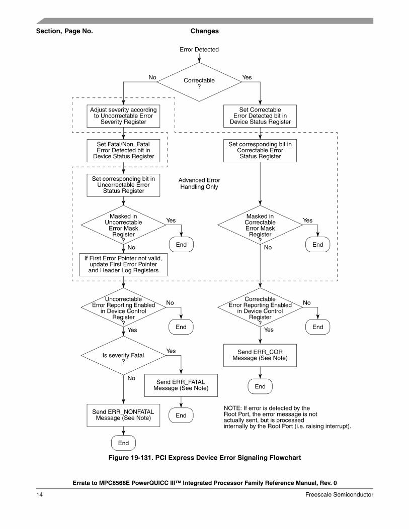
19.4.1.10, 19-106 Added the following section:
19.4.1.10 Error Handling
The PCI Express specification classifies errors as correctable and uncorrectable. Correctable errors result in degraded performance, but uncorrectable errors generally result in functional failures. As shown in Figure 19-130 uncorrectable errors can further be classified as fatal or non-fatal.

Section, Page No. Changes
Errata to MPC8568E PowerQUICC III™ Integrated Processor Family Reference Manual, Rev. 0
Freescale Semiconductor 13
Figure 19-130. PCI Express Error Classification
19.4.1.10.1 PCI Express Error Logging and Signaling
Figure 19-131 shows the PCI Express-defined sequence of operations related to signaling and logging of errors detected by a device. Note that the PCI Express controller on this device supports the advanced error handling capabilities shown within the dotted lines.
Physical
Data Link Transaction
Correctable Errors
ERR_COR
Physical
Transaction
Uncorrectable Errors
ERR_NONFATAL
Data Link
ERR_FATAL
Fatal
Section, Page No. Changes
Errata to MPC8568E PowerQUICC III™ Integrated Processor Family Reference Manual, Rev. 0
14 Freescale Semiconductor
Figure 19-131. PCI Express Device Error Signaling Flowchart
If First Error Pointer not valid,update First Error Pointerand Header Log Registers
Set corresponding bit inUncorrectable Error
Status Register
Masked inUncorrectable
Error MaskRegister
?
Set Fatal/Non_FatalError Detected bit in
Device Status Register
Adjust severity accordingto Uncorrectable Error
Severity Register
UncorrectableError Reporting Enabled
in Device ControlRegister
?
Is severity Fatal?
Send ERR_NONFATALMessage (See Note)
Send ERR_FATALMessage (See Note)
End
End
End
Send ERR_CORMessage (See Note)
CorrectableError Reporting Enabled
in Device ControlRegister
?
Masked inCorrectableError Mask
Register?
End
Set corresponding bit inCorrectable ErrorStatus Register
Set CorrectableError Detected bit in
Device Status Register
End
End
Correctable?
Error Detected
NOTE: If error is detected by theRoot Port, the error message is notactually sent, but is processedinternally by the Root Port (i.e. raising interrupt).
End
YesNo
Yes
No
Yes
No
Yes
No
Yes
No
No
Yes
Advanced ErrorHandling Only

Section, Page No. Changes
Errata to MPC8568E PowerQUICC III™ Integrated Processor Family Reference Manual, Rev. 0
Freescale Semiconductor 15
19.4.1.10.2 PCI Express Controller Internal Interrupt Sources
Table 19-125 describes the sources of the PCI Express controller internal interrupt to the PIC and the preconditions for signaling the interrupt.
Table 19-125. PCI Express Internal Controller Interrupt Sources
Status Register Bit Preconditions
Any bit in PEX_PME_MES_DR set The corresponding interrupt enable bits must be set in PEX_PME_MES_IER
Any bit in PEX_ERR_DR set The corresponding interrupt enable bits must be set in PEX_ERR_EN.
PCI Express Root Status Register[16] (PME status) is set
PCI Express Root Control Register [3] (PME interrupt enable) is set
PCI Express Root Error Status Register[6] (fatal error messages received) is set
PCI Express Root Error Command Register [2] (fatal error reporting enable) is set orPCI Express Root Control Register [2] (system error on fatal error enable) is set
PCI Express Root Error Status Register [5] (non-fatal error messages received) is set
PCI Express Root Error Command Register [1] (non-fatal error reporting enable) is set or PCI Express Root Control Register [1] (system error on non-fatal error enable) is set
PCI Express Root Error Status Register[0] (correctable error messages received) is set
PCI Express Root Error Command Register[0] (correctable error reporting enable) is setor PCI Express Root Control Register[0] (system error on correctable error enable) is set.
Any correctable error status bit in PCI Express Correctable Error Status Register is set
The corresponding error mask bit in PCI Express Correctable Error Mask Register is clear and PCI Express Root Error Command Register[0] (correctable error reporting enable) is set
Any fatal uncorrectable error status bit in PCI Express Uncorrectable Error Status Register is set. (The corresponding error is classified as fatal based on the severity setting in PCI Express Uncorrectable Error Severity Register.)
The corresponding error mask bit in PCI Express Uncorrectable Error Mask Register is clear and either PCI Express Device Control Register[2] (fatal error reporting) is set or PCI Express Command Register[8] (SERR) is set.
Any non-fatal uncorrectable error status bit in PCI Express Uncorrectable Error Status Register is set. (The corresponding error is classified as non-fatal based on the severity setting in PCI Express Uncorrectable Error Severity Register.)
The corresponding error mask bit in PCI Express Uncorrectable Error Mask Register is clear and either PCI Express Device Control Register[1] (non-fatal error reporting) is set or PCI Express Command Register[8] (SERR) is set.
PCI Express Secondary Status Register[8] (master data parity error) is set.
PCI Express Secondary Status Interrupt Mask Register[0] (mask master data parity error) is cleared and PCI Express Command Register[6] (parity error response) is set.
PCI Express Secondary Status Register[11] (signaled target abort) is set
PCI Express Secondary Status Interrupt Mask Register[1] (mask signaled target abort) is cleared.
PCI Express Secondary Status Register[12] (received target abort) is set
PCI Express Secondary Status Interrupt Mask Register[2] (mask received target abort) is cleared.

Section, Page No. Changes
Errata to MPC8568E PowerQUICC III™ Integrated Processor Family Reference Manual, Rev. 0
16 Freescale Semiconductor
PCI Express Secondary Status Register[13] (received master abort) is set
PCI Express Secondary Status Interrupt Mask Register[3] (mask received master abort) is cleared.
PCI Express Secondary Status Register[14] (signaled system error) is set.
PCI Express Secondary Status Interrupt Mask Register[4] (mask signaled system error) is cleared.
PCI Express Secondary Status Register[15] (detected parity error) is set
PCI Express Secondary Status Interrupt Mask Register[5] (mask detected parity error) is cleared.
PCI Express Slot Status Register[0] (attention button pressed) is set
PCI Express Slot Control Register[0] (attention button pressed enable) is set and PCI Express Slot Control Register[5] (hot plug interrupt enable) is set and either PCI Express PM Control Register[1–0] = 00 (the function power state is D0) or PCI Express PM Control Register[8] (PME enable) is set.
PCI Express Slot Status Register[1] (power fault detected) is set
PCI Express Slot Control Register[1] (power fault detected enable) is set and PCI Express Slot Control Register[5] (hot plug interrupt enable) is set and either PCI Express PM Control Register[1–0] = 00 (the function power state is D0) or PCI Express PM Control Register[8] (PME enable) is set.
PCI Express Slot Status Register[2] (MRL sensor changed) is set
PCI Express Slot Control Register[2] (MRL sensor changed enable) is set and PCI Express Slot Control Register[5] (hot plug interrupt enable) is set and either PCI Express PM Control Register[1–0] = 00 (the function power state is D0) or PCI Express PM Control Register[8] (PME enable) is set.
PCI Express Slot Status Register[3] (presence detect changed) is set
PCI Express Slot Control Register[3] (presence detect changed enable) is set and PCI Express Slot Control Register[5] (hot plug interrupt enable) is set and either PCI Express PM Control Register[1–0] = 00 (the function power state is D0) or PCI Express PM Control Register[8] (PME enable) is set.
PCI Express Slot Status Register[4] (command completed) is set
PCI Express Slot Control Register[4] (command completed interrupt enable) is set and PCI Express Slot Control Register[5] (hot plug interrupt enable) is set.
Table 19-125. PCI Express Internal Controller Interrupt Sources (continued)
Status Register Bit Preconditions

Section, Page No. Changes
Errata to MPC8568E PowerQUICC III™ Integrated Processor Family Reference Manual, Rev. 0
Freescale Semiconductor 17
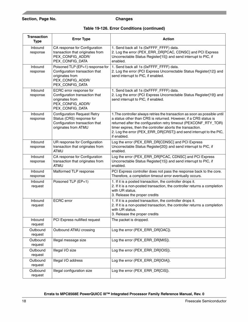
19.4.1.10.3 Error Conditions
Table 19-126 describes specific error types and the action taken for various transaction types.
Table 19-126. Error Conditions
Transaction Type
Error Type Action
Inbound response
PEX response time out. This case happens when the internal platform sends a non-posted request that did not get a response back after a specific amount of time specified in the outbound completion timeout register (PEX_OTB_CPL_TOR)
Log error (PEX_ERR_DR[PCT]) and send interrupt to PIC, if enabled.
Inbound response
Unexpected PEX response. This can happen if, after the response times out and the internal queue entry is deallocated, the response comes back.
Log unexpected completion error (PCI Express Uncorrectable Status Register[16]).
Inbound response
Unsupported request (UR) response status
Depending upon whether the initial internal request was broken up, the error is not sent until all responses come back for all portions of the internal request. Log the error (PEX_ERR_DR[CDNSC] and PCI Express Uncorrectable Status Register[20]) and send interrupt to PIC, if enabled.
Inbound response
Completer abort (CA) response status
Depending upon whether the initial internal request was broken up, the error is not sent until all responses come back for all portions of the internal request. Log the error (PEX_ERR_DR[PCAC, CDNSC] and PCI Express Uncorrectable Status Register[15] and send interrupt to PIC, if enabled.
Inbound response
Poisoned TLP (EP=1) Depending upon whether the initial internal request was broken up, the error is not sent until all responses come back for all portions of the internal request. Log the error (PCI Express Uncorrectable Status Register[12]) and send interrupt to PIC, if enabled.
Inbound response
ECRC error Depending upon whether the initial internal request was broken up, the error is not sent until all responses come back for all portions of the internal request. Log the error (PCI Express Uncorrectable Status Register[19]) and send interrupt to PIC, if enabled.
Inbound response
Configuration Request Retry Status (CRS) timeout for a configuration transaction that originates from PEX_CONFIG_ADDR/PEX_CONFIG_DATA
1.The controller always retries the transaction as soon as possible until a status other than CRS is returned. However, if a CRS status is returned after the configuration retry timeout (PEXCONF_RTY_TOR) timer expires, then the controller aborts the transaction and sends all 1s (0xFFFF_FFFF) data back to requester. 2. Log the error (PEX_ERR_DR[PCT]) and send interrupt to the PIC, if enabled.
Inbound response
UR response for configuration transaction that originates from PEX_CONFIG_ADDR/PEX_CONFIG_DATA
1. Send back all 1s (0xFFFF_FFFF) data.2. Log the error (PEX_ERR_DR[CDNSC] and PCI Express Uncorrectable Status Register[20]) and send interrupt to PIC, if enabled.
Section, Page No. Changes
Errata to MPC8568E PowerQUICC III™ Integrated Processor Family Reference Manual, Rev. 0
18 Freescale Semiconductor
Inbound response
CA response for Configuration transaction that originates from PEX_CONFIG_ADDR/PEX_CONFIG_DATA
1. Send back all 1s (0xFFFF_FFFF) data.2. Log the error (PEX_ERR_DR[PCAC, CDNSC] and PCI Express Uncorrectable Status Register[15]) and send interrupt to PIC, if enabled.
Inbound response
Poisoned TLP (EP=1) response for Configuration transaction that originates from PEX_CONFIG_ADDR/PEX_CONFIG_DATA
1. Send back all 1s (0xFFFF_FFFF) data.2. Log the error (PCI Express Uncorrectable Status Register[12]) and send interrupt to PIC, if enabled.
Inbound response
ECRC error response for Configuration transaction that originates from PEX_CONFIG_ADDR/PEX_CONFIG_DATA
1. Send back all 1s (0xFFFF_FFFF) data.2. Log the error (PCI Express Uncorrectable Status Register[19]) and send interrupt to PIC, if enabled.
Inbound response
Configuration Request Retry Status (CRS) response for Configuration transaction that originates from ATMU
1.The controller always retries the transaction as soon as possible until a status other than CRS is returned. However, if a CRS status is returned after the configuration retry timeout (PEXCONF_RTY_TOR) timer expires, then the controller aborts the transaction. 2. Log the error (PEX_ERR_DR[CRST]) and send interrupt to the PIC, if enabled.
Inbound response
UR response for Configuration transaction that originates from ATMU
Log the error (PEX_ERR_DR[CDNSC] and PCI Express Uncorrectable Status Register[20]) and send interrupt to PIC, if enabled.
Inbound response
CA response for Configuration transaction that originates from ATMU
Log the error (PEX_ERR_DR[PCAC, CDNSC] and PCI Express Uncorrectable Status Register[15]) and send interrupt to PIC, if enabled.
Inbound response
Malformed TLP response PCI Express controller does not pass the response back to the core. Therefore, a completion timeout error eventually occurs.
Inbound request
Poisoned TLP (EP=1) 1. If it is a posted transaction, the controller drops it. 2. If it is a non-posted transaction, the controller returns a completion with UR status.3. Release the proper credits
Inbound request
ECRC error 1. If it is a posted transaction, the controller drops it. 2. If it is a non-posted transaction, the controller returns a completion with UR status.3. Release the proper credits
Inbound request
PCI Express nullified request The packet is dropped.
Outbound request
Outbound ATMU crossing Log the error (PEX_ERR_DR[OAC]).
Outbound request
Illegal message size Log the error (PEX_ERR_DR[MIS]).
Outbound request
Illegal I/O size Log the error (PEX_ERR_DR[IOIS]).
Outbound request
Illegal I/O address Log the error (PEX_ERR_DR[IOIA]).
Outbound request
Illegal configuration size Log the error (PEX_ERR_DR[CIS]).
Table 19-126. Error Conditions (continued)
Transaction Type
Error Type Action

Section, Page No. Changes
Errata to MPC8568E PowerQUICC III™ Integrated Processor Family Reference Manual, Rev. 0
Freescale Semiconductor 19
19.4.6, 19-115 Added the following section:
19.4.6 Link Down
Typically, a link down condition occurs after a hot reset event; however, it is possible for the link to go down unexpectedly without a hot reset event. When this occurs, a link down condition is detected (PEX_PME_MSG_DR[LDD]=1). Link down is treated similarly to a hot reset condition.
Subsequently, while the link is down, all new posted outbound transactions are discarded. All new non-posted ATMU transactions are errored out. Non-posted configuration transactions issued using PEX_CONFIG_ADDR/PEX_CONFIG_DATA toward the link returns 0xFFFF_FFFF (all 1s). As soon as the link is up again, the sending of transaction resumes.
Note that in EP mode, a link down condition causes the controller to reset all non-sticky bits in its PCI Express configuration registers as if it had been hot reset. 20.2, 20-10 In Table 20-3, “SEC Address Map,” corrected address offset of AESU context
memory registers and AESU key memory registers in memory map, as follows:Former address offset:
AESU context memory registers = 0x3_4100–0x3_4108AESU key memory registers = 0x3_4400–0x3_4408
New address offset:AESU context memory registers = 0x3_4100–0x3_4137AESU key memory registers = 0x3_4400–0x3_441F
20.4.7, 20-80 Clarified explanatory text for the data size register, the IV1 and IV2 registers, the context data registers, and the key data registers.
20.4.7.14, 20-92 Made all KEU key data registers as write-only in Figure 20-69, “KEU Key Data Register_1 (CK-high)” and Figure 20-70, “KEU Key Data Register_2 (CK-low)”
20.4.7.15, 20-92 Made all KEU key data registers as write-only in Figure 20-71, “KEU Key Data Register_3 (IK-high)” and Figure 20-72, “KEU Key Data Register_4 (IK-low)”
21.4.1.6, 21-12 In Figure 21-6, “POR Bringup Mode Status Register (PORBUPMSR),” corrected the reset value for POR bringup mode status register (PORBUPMSR)In Table 21-9, “PORBUPMSR Field Descriptions,” corrected the description of the DEV_TYPE field as follows:Device type. Indicates the device type.
Outbound response
Internal platform response with error (for example, an ECC error on a DDR read or the transaction maps to unknown address space).
Send poisoned TLP (EP=1) completion(s) for data that are known bad. If the poison data happens in the middle of the packet, the rest of the response packet(s) is also poisoned.
Table 19-126. Error Conditions (continued)
Transaction Type
Error Type Action

Section, Page No. Changes
Errata to MPC8568E PowerQUICC III™ Integrated Processor Family Reference Manual, Rev. 0
20 Freescale Semiconductor
0 MPC8568E or MPC85681 MPC8567E or MPC8567
21.4.1.11, 21-16 Clarified the introductory paragraph (Section 21.4.1.11, “Alternate Function Signal Multiplex Control Register (PMUXCR)”) by modifying the second sentence as follows:Signal multiplexing not controlled by this register is handled separately through the QUICC Engine Block programming model described in Section 21.5.3, “QUICC Engine Block I/O Ports.”
21.4.1.15, 21-21 Updated the description of the reset request status and control register (RSTRSCR) as follows:“Shown in Figure 21-15, the RSTRSCR contains status bits to record the reasons for HRESET_REQ assertion as well as a mask bit to exclude RapidIO packets from generating such a reset request.”.
21.4.1.20, 21-24 Added a cross-reference to Section 3.4.4, “Ports Tables”21.4.1.22, 21-26 Added a cross-reference to Section 3.4.4, “Ports Tables”21.4.1.23, 21-27 Added a cross-reference to Section 3.4.4, “Ports Tables”21.5.4, 21-41 Corrected signal functionality multiplexing for PC[18] and PC[19] as follows:
PC[18] is multiplexed with IIC2_SCLPC[19] is multiplexed with IIC2_SDA
22.4.7, 22-15 In Table 22-10, “Performance Monitor Events,” clarified that PCI performance monitor event counts are only accurate when PCI controller is configured in synchronous operation
24.2.6, 24-8 Added the following section:
24.2.6 Serial Interface with Time-Slot Assigner
The information in this MPC8568E-specific “Serial Interface with Time-Slot Assigner” subsection applies throughout the QERM “Serial Interface with Time-Slot Assigner” chapter.
• High-speed operation for UCC entries is not applicable to MPC8568E• The registers used for high-speed operation for UCC entries—SI Speed Register (SISPD) and SI
Tx Clock Edge Invert (SITCEI)—are not supported.
Section, Page No. Changes
Errata to MPC8568E PowerQUICC III™ Integrated Processor Family Reference Manual, Rev. 0
Freescale Semiconductor 21
THIS PAGE INTENTIONALLY LEFT BLANK

Section, Page No. Changes
Errata to MPC8568E PowerQUICC III™ Integrated Processor Family Reference Manual, Rev. 0
22 Freescale Semiconductor
THIS PAGE INTENTIONALLY LEFT BLANK

Section, Page No. Changes
Errata to MPC8568E PowerQUICC III™ Integrated Processor Family Reference Manual, Rev. 0
Freescale Semiconductor 23
THIS PAGE INTENTIONALLY LEFT BLANK

Document Number: MPC8568ERMADRev. 0.106/2008
Information in this document is provided solely to enable system and software
implementers to use Freescale Semiconductor products. There are no express or
implied copyright licenses granted hereunder to design or fabricate any integrated
circuits or integrated circuits based on the information in this document.
Freescale Semiconductor reserves the right to make changes without further notice to
any products herein. Freescale Semiconductor makes no warranty, representation or
guarantee regarding the suitability of its products for any particular purpose, nor does
Freescale Semiconductor assume any liability arising out of the application or use of
any product or circuit, and specifically disclaims any and all liability, including without
limitation consequential or incidental damages. “Typical” parameters which may be
provided in Freescale Semiconductor data sheets and/or specifications can and do
vary in different applications and actual performance may vary over time. All operating
parameters, including “Typicals” must be validated for each customer application by
customer’s technical experts. Freescale Semiconductor does not convey any license
under its patent rights nor the rights of others. Freescale Semiconductor products are
not designed, intended, or authorized for use as components in systems intended for
surgical implant into the body, or other applications intended to support or sustain life,
or for any other application in which the failure of the Freescale Semiconductor product
could create a situation where personal injury or death may occur. Should Buyer
purchase or use Freescale Semiconductor products for any such unintended or
unauthorized application, Buyer shall indemnify and hold Freescale Semiconductor
and its officers, employees, subsidiaries, affiliates, and distributors harmless against all
claims, costs, damages, and expenses, and reasonable attorney fees arising out of,
directly or indirectly, any claim of personal injury or death associated with such
unintended or unauthorized use, even if such claim alleges that Freescale
Semiconductor was negligent regarding the design or manufacture of the part.
How to Reach Us:
Home Page: www.freescale.com
Web Support: http://www.freescale.com/support
USA/Europe or Locations Not Listed: Freescale Semiconductor, Inc.Technical Information Center, EL5162100 East Elliot Road Tempe, Arizona 85284 1-800-521-6274 or+1-480-768-2130www.freescale.com/support
Europe, Middle East, and Africa:Freescale Halbleiter Deutschland GmbHTechnical Information CenterSchatzbogen 781829 Muenchen, Germany+44 1296 380 456 (English) +46 8 52200080 (English)+49 89 92103 559 (German)+33 1 69 35 48 48 (French) www.freescale.com/support
Japan: Freescale Semiconductor Japan Ltd. HeadquartersARCO Tower 15F1-8-1, Shimo-Meguro, Meguro-ku Tokyo 153-0064Japan 0120 191014 or+81 3 5437 [email protected]
Asia/Pacific: Freescale Semiconductor China Ltd. Exchange Building 23FNo. 118 Jianguo RoadChaoyang DistrictBeijing 100022China+86 10 5879 [email protected]
For Literature Requests Only:Freescale Semiconductor
Literature Distribution Center P.O. Box 5405Denver, Colorado 80217 1-800 441-2447 or+1-303-675-2140Fax: +1-303-675-2150LDCForFreescaleSemiconductor
@hibbertgroup.com
Freescale and the Freescale logo are trademarks or registered trademarks of Freescale Semiconductor, Inc. in the U.S. and other countries. All other product or service names are the property of their respective owners. The Power Architecture and Power.org word marks and the Power and Power.org logos and related marks are trademarks and service marks licensed by Power.org. The PowerPC name is a trademark of IBM Corp. and is used under license. RapidIO is a registered trademark of the RapidIO Trade Association. IEEE 802.1, 802.1Q, 802.1p, 802.3, 802.3u, 802.3x, 802.3z, 802.3ac, 802.3ab, and 1588 are trademarks or registered trademarks of the Institute of Electrical and Electronics Engineers, Inc. (IEEE). This product is not endorsed or approved by the IEEE.
© Freescale Semiconductor, Inc., 2008. All rights reserved.