Embed Size (px)
Citation preview

i
Development of an Electrochemical Micromachining (µECM) machine
A Thesis Submitted for the Degree of doctor of Philosophy
By
Alexandre SPIESER
College of Engineering, Design and Physical Sciences
Brunel University
London, United Kingdom
March 2015

ii
ABSTRACT Electrochemical machining (ECM) and especially electrochemical micromachining
(µECM) became an attractive area of research due to the fact that this process does not
create any defective layer after machining and that there is a growing demand for better
surface integrity on different micro applications such as microfluidics systems and stress-
free drilled holes in the automotive and aerospace sectors.
Electrochemical machining is considered as a non-conventional machining process based
on the phenomenon of electrolysis. This process requires maintaining a small gap - the
interelectrode gap (IEG) - between the anode (workpiece) and the cathode (tool-electrode)
in order to achieve acceptable machining results (i.e. accuracy, high aspect ratio with
appropriate material removal rate and efficiency).
This work presents the design of a next generation µECM machine for the automotive,
aerospace, medical and metrology sectors. It has 3 axes of motion (X, Y and Z) and a spindle
allowing the tool-electrode to rotate during machining.
The linear slides for each axis use air bearings with linear DC brushless motors and 2nm-
resolution encoders for ultra-precise motion. The control system is based on the Power
PMAC motion controller from Delta Tau. The electrolyte tank is located at the rear of the
machine and allows the electrolyte to be changed quickly.
A pulse power supply unit (PSU) and a special control algorithm have been implemented.
The pulse power supply provides not only ultra-short pulses (50ns), but also plus and minus
biases as well as a polarity switching functionality. It fulfils the requirements of tool
preparation with reversed ECM on the machine. Moreover, the PSU is equipped with an
ultrafast over current protection which prevents the tool-electrode from being damaged in
case of short-circuits.
Two different process control algorithms were made: one is fuzzy logic based and the other
is adapting the feed rate according to the position and time at which short-circuits were
detected.
The developed machine is capable of drilling micro holes in hard-to-machine materials but
also machine micro-styli and micro-needles for the metrology (micro CMM) and medical
sectors. This work also presents drilling trials performed with the machine with an orbiting

iii
tool. Machining experiments were also carried out using electrolytes made of a combination
of HCl and NaNO aqueous solutions.
The developed machine was used to fabricate micro tools out of 170µm WC-Co alloy shafts
via micro electrochemical turning and drill deep holes via µECM in disks made of 18NiCr6
alloy.
Results suggest that this process can be used for industrial applications for hard-to-machine
materials. The author also suggests that the developed machine can be used to manufacture
micro-probes and micro-tools for metrology and micro-manufacturing purposes.
Keywords — Micro ECM, PECM, micromanufacturing, micro ECM machines,
electrochemical micromachining (EMM)

iv
ACKNOWLEDGEMENTS I would like to express my deepest gratitude to the people who have helped and guided in
working to realize this research project.
Firstly, I would like to thank my supervisor, Dr. Atanas IVANOV, for his guidance,
assistance, time, effort and never ending patience to make this project a success.
Not forgetting Andreas Rohrmeier, Rebecca Leese, Martin Santl and Paul Yates for their
support and help through one-on-one or group meetings.
I also would like to thank the Delta Tau support team who took the time to answer my
questions.
I would like also thank Brunel University and the European Commission for financing my
PhD studies. I am thankful to the EU FP7 Micro-ECM and EU FP7 MIDEMMA projects’
partners for the constructive discussions.
I would also like to express my gratitude to my family for supporting me and providing me
endless encouragement and my girlfriend for her support and motivation. Lastly, I would
like to thank my friends and colleagues for all their help and support.
This project is dedicated to those mentioned above.

v
TABLE OF CONTENT
ABSTRACT .............................................................................................................................. II
ACKNOWLEDGEMENTS ...................................................................................................... IV
TABLE OF CONTENT .............................................................................................................. V
LIST OF FIGURES ................................................................................................................. XII
LIST OF TABLES ................................................................................................................... XX
LIST OF ABBREVIATIONS................................................................................................. XXI
LIST OF SYMBOLS ........................................................................................................... XXIV
CHAPTER 1: INTRODUCTION ............................................................................................. 1
1.1. From ECM to µECM ............................................................................................................. 1
1.2. Justification, Aims and Objectives ......................................................................................... 2 1.2.1. Justification ................................................................................................................. 2 1.2.2. Aims ........................................................................................................................... 4 1.2.3. Objectives ................................................................................................................... 4
1.3. Methodology ......................................................................................................................... 5 1.3.1. Identification of gaps in research and key requirements for µECM............................... 5 1.3.2. Development of a simulation programme to investigate the µECM process behaviour . 7 1.3.3. Development of a novel pulse PSU architecture for the needs of µECM....................... 7 1.3.4. Component selection and machine system integration .................................................. 8 1.3.5. Development of an innovative control strategy for the µECM process ......................... 9 1.3.6. Development of an intelligent HMI ........................................................................... 10 1.3.7. Experimental validation ............................................................................................. 10
1.4. Description of chapters ........................................................................................................ 10
1.5. Key contributions ................................................................................................................ 12
CHAPTER 2: LITERATURE REVIEW ............................................................................... 15
2.1. Introduction ......................................................................................................................... 15
2.2. ECM Fundamentals ............................................................................................................. 17

vi
2.2.1. Basic ECM setup ....................................................................................................... 17 2.2.2. The chemical reaction ................................................................................................ 18 2.2.3. The material removal rate (MRR) .............................................................................. 19
2.2.3.1. MRR for pure materials (non-alloy) .................................................................. 19 2.2.3.2. MRR for alloys in ECM .................................................................................... 21
2.3. Machining process............................................................................................................... 21 2.3.1. Review and analysis of the ECM and µECM machines available on the market ......... 21 2.3.2. Design requirements and constraints for µECM systems ............................................ 23
2.3.2.1. Ultra-precision motion for tool-positioning........................................................ 23 2.3.2.1. High dynamics and frictionless motion .............................................................. 24 2.3.2.2. Workpiece clamping and tool holder constraints ................................................ 24
2.3.3. Process monitoring and control .................................................................................. 25 2.3.3.1. Interelectrode gap control and optimization algorithms ...................................... 26 2.3.3.2. The electrical double layer (EDL) effect in µECM ............................................ 31 2.3.3.3. Control of the voltage at the electrodes .............................................................. 35
2.3.4. Machining strategies .................................................................................................. 36
2.4. Pulse power supply unit (PSU) considerations ..................................................................... 38
2.5. Electrode and workpiece preparation ................................................................................... 41 2.5.1. Tool design software ................................................................................................. 41 2.5.2. Off-Machine electrode fabrication ............................................................................. 42 2.5.3. On-Machine electrode preparation ............................................................................. 43 2.5.4. Electrical connections ................................................................................................ 45
2.6. Measurement ....................................................................................................................... 46 2.6.1. Measuring dimensions ............................................................................................... 46 2.6.2. Machine set-up .......................................................................................................... 47 2.6.3. Surface roughness ..................................................................................................... 48
2.6.3.1. Influence of the electrolyte ................................................................................ 48 2.6.3.2. Material grain structure and composition ........................................................... 50 2.6.3.3. Influence of electrical parameters ...................................................................... 50
2.7. Handling ............................................................................................................................. 51 2.7.1. Electrodes and workpiece .......................................................................................... 51 2.7.2. Electrolytes ............................................................................................................... 51
2.8. Discussion and conclusions ................................................................................................. 54
CHAPTER 3: µECM PROCESS MODELLING AND SIMULATION ................................ 57
3.1. Inter-electrode gap behaviour without feed rate.................................................................... 57
3.2. Bin Wei’s PECM gap model with constant feed rate ............................................................ 61 3.2.1. Mathematical formulation.......................................................................................... 61 3.2.2. Simulation ................................................................................................................. 62 3.2.3. Concluding remarks regarding Bin Wei’s model with constant feed rate .................... 67

vii
3.3. µECM model according to Marla et al. ................................................................................ 67
3.4. The electrical double layer: study of existing models and simulation .................................... 69 3.4.1. Models of the electrical double layer effect on the gap voltage ................................... 69 3.4.2. Similarities with Zener diodes ................................................................................... 71 3.4.3. More realistic model of the IEG ................................................................................. 75
3.5. 2D Drilling simulation with simple electrical double layer (EDL) model .............................. 77 3.5.1. Point to point inter-electrode gap (h) calculation method............................................ 78 3.5.2. Modelling the influence of the EDL on the gap change .............................................. 79 3.5.3. Simulation workflow ................................................................................................. 80
3.6. Influence of the pulse frequency on the localization and the machining time. ....................... 83
3.7. Summary ............................................................................................................................. 85
CHAPTER 4: AN INNOVATIVE PULSE POWER SUPPLY UNIT FOR µECM ............. 86
4.1. An novel pulse PSU architecture ......................................................................................... 86
4.2. Previous prototypes ............................................................................................................. 87 4.2.1. First prototype ........................................................................................................... 88 4.2.2. Second prototype ....................................................................................................... 88
4.3. Pulse PSU prototype modules .............................................................................................. 89 4.3.1. The control circuitry .................................................................................................. 89
4.3.1.1. Pulse generating module ................................................................................... 89 4.3.1.2. Pulse shape selection ......................................................................................... 91 4.3.1.3. 24V-logic isolated digital interface .................................................................... 93
4.3.2. The power stage ........................................................................................................ 94 4.3.2.1. Configuration .................................................................................................... 94 4.3.2.2. MOSFET selection ............................................................................................ 95 4.3.2.3. Driver selection ................................................................................................. 96 4.3.2.4. Optimized layout for smaller footprint and reduced parasitics ............................ 97
4.3.3. The over current protection (OCP) stage .................................................................... 98 4.3.1. PSU testing and mounting ........................................................................................100
4.3.1.1. On-board signals ..............................................................................................105 4.3.1.2. OCP triggering trials ........................................................................................106
4.3.2. Operation of the third PSU prototype ........................................................................109
4.4. Discussion and conclusion for Chapter 3 ............................................................................110
CHAPTER 5: MACHINE SYSTEM INTEGRATION ....................................................... 111
5.1. Granite base .......................................................................................................................112
5.2. X, Y and Z Slides ...............................................................................................................113 5.2.1. The linear DC brushless motor .................................................................................114 5.2.2. Encoder system ........................................................................................................115

viii
5.2.3. The air bearings ........................................................................................................116
5.3. The spindle .........................................................................................................................116
5.4. Electrical cabinet ................................................................................................................119 5.4.1. Control components .................................................................................................119
5.4.1.1. Power PMAC motion controller .......................................................................119 5.4.1.2. ACC24E-2 4 axes interface board ....................................................................120 5.4.1.3. ACC36UK 16bit Analogue input board ............................................................121 5.4.1.4. ACC65E digital input/output board ..................................................................123
5.4.1. GeoDrive direct PWM amplifiers .............................................................................124 5.4.2. 24V logic and electrical Safety components ..............................................................125
5.4.2.1. 24V logic components ......................................................................................125 5.4.2.2. Circuit breakers ................................................................................................126
5.4.3. Filtering and shielding ..............................................................................................126
5.5. Electrochemical machining cell and electrical connections..................................................126
5.6. Electrolyte circuit ...............................................................................................................129
5.7. Conclusions ........................................................................................................................130
CHAPTER 6: PROCESS CONTROL AND SUPERVISION ............................................. 131
6.1. Servo loop tuning of the X, Y and Z axes............................................................................131
6.2. Orbiting motion ..................................................................................................................134
6.3. Machine initialization algorithms ........................................................................................135
6.4. Process control algorithms ..................................................................................................136 6.4.1. The state machine .....................................................................................................137 6.4.1. The gap initialisation algorithm ................................................................................138 6.4.2. Machining process control algorithms.......................................................................140
6.4.2.1. IEG control using fuzzy logic ...........................................................................140 6.4.2.2. Adaptive feed rate algorithm ............................................................................146 6.4.2.3. Escape strategy ................................................................................................148
6.5. An intelligent Human Machine Interface (HMI) .................................................................151
6.6. Conclusions ........................................................................................................................156
CHAPTER 7: EXPERIMENTAL WORK AND RESULTS ............................................... 157
7.1. Experimental work at Sonplas GmbH on the machine developed in 2013 (Germany) ..........157 7.1.1. Discussion on the setup ............................................................................................157 7.1.2. Experiments and results ............................................................................................159
7.1.2.1. Effect of frequency on the hole shape ...............................................................159 7.1.2.2. Drilling with orbiting electrode ........................................................................160

ix
7.1.2.1. Gasoline injector drilling ..................................................................................163 7.1.2.1. Damaged electrodes due to sparking .................................................................165
7.1.3. Process behaviour with the fuzzy logic control algorithm ..........................................165
7.2. Drilling experiments with orbiting tool-electrode ................................................................166
7.3. Investigation on the effect of pulse frequency, duty cycle and voltage on the machining performance ..............................................................................................................................171
7.3.1. Methodology ............................................................................................................171 7.3.2. Results .....................................................................................................................172 7.3.3. Discussion on the effect of pulse frequency, duty cycle and voltage on the machining performance ..........................................................................................................................177 7.3.4. Verification of the µECM LabVIEW simulation model ............................................178
7.4. On-line tool fabrication followed by workpiece drilling ......................................................180
7.5. Micro-Tool fabrication .......................................................................................................183
CHAPTER 8: CONCLUSIONS AND FUTURE WORK .................................................... 186
8.1. Conclusions ........................................................................................................................186
8.2. Contributions to knowledge ................................................................................................189
8.3. Recommendations for future work ......................................................................................191
REFERENCES ...................................................................................................................... 192
LIST OF FIGURES IN APPENDICES................................................................................. 205
LIST OF TABLES IN APPENDICES .................................................................................. 208
APPENDIX 1. LIST OF PUBLICATIONS .......................................................................... 209
APPENDIX 2. CALCULATION OF 퐊퐯 퐚퐥퐥퐨퐲 FOR 100CR6 ........................................... 210
APPENDIX 3. POWER ELECTRONICS FUNDAMENTALS ........................................... 211
Appendix 3.1. Structure of a pulse power supply unit ................................................................211 Appendix 3.1.1. Microcontroller ...........................................................................................211
Appendix 3.1.1.1. On-board I2C communication ..............................................................211 Appendix 3.1.1.2. On-board SPI communication ...............................................................212 Appendix 3.1.1.3. Modulation ...........................................................................................212
Appendix 3.1.2. The power part of a pulse power supply unit ................................................213 Appendix 3.1.2.1. MOSFET basics ...................................................................................213 Appendix 3.1.2.2. Reducing ringing at the MOSFET switch nodes using snubbers ............215
Appendix 3.1.3. Isolation between control and power parts ...................................................217

x
Appendix 3.1.4. Current sensing for over-current protection ..................................................217 Appendix 3.1.5. Board design considerations and assembly ...................................................218
APPENDIX 4. DEVELOPMENT OF THE FIRST PULSE PSU PROTOTYPE ............... 221
Appendix 4.1. First prototype: General presentation ..................................................................221
Appendix 4.2. First prototype: The control circuitry ..................................................................221
Appendix 4.3. First prototype: The power stage .........................................................................230 Appendix 4.3.1. Timing aspects of the control signals ...........................................................230 Appendix 4.3.2. MOSFET selection ......................................................................................232 Appendix 4.3.3. Driver selection ...........................................................................................233 Appendix 4.3.4. Power electronics board layout ....................................................................234
Appendix 4.4. First prototype: The current sensing board ..........................................................236 Appendix 4.4.1. Over current protection (OCP) .....................................................................236 Appendix 4.4.2. The peak detector ........................................................................................237 Appendix 4.4.3. First prototype: firmware programming .......................................................238
Appendix 4.5. Tests and conclusion on first prototype ...............................................................241 Appendix 4.5.1. Measuring the PSU output and the influence of cabling ...............................241 Appendix 4.5.2. On-board signal measurement .....................................................................243 Appendix 4.5.3. Conclusions regarding the first PSU prototype .............................................244
APPENDIX 5. PULSE PSU SIMULATION WITH MATLAB/SIMULINK ..................... 245
Appendix 5.1. Basic model (ideal) .............................................................................................245
Appendix 5.2. Realistic model (including parasitics) .................................................................246
APPENDIX 6. SECOND PULSE PSU PROTOTYPE ........................................................ 248
Appendix 6.1. Second PSU prototype: control circuitry .............................................................248 Appendix 6.1.1. Pulse generating module ..............................................................................248 Appendix 6.1.2. Pulse shape selection ...................................................................................249 Appendix 6.1.3. Avoiding MOSFET cross conduction ..........................................................252
Appendix 6.2. Second PSU prototype: power stage ...................................................................253
Appendix 6.3. Second PSU prototype: over current protection (OCP) stage ...............................262
APPENDIX 7. EXPERIMENTAL WORK AT BRUNEL USING A TEST STAND .......... 264
Appendix 7.1. Planning of experiment and experimental setup ..................................................264 Appendix 7.1.1. Materials and equipment used......................................................................265 Appendix 7.1.2. Interelectrode gap (IEG) initialization ..........................................................266 Appendix 7.1.3. Tool approach and gap initialization on the test stand ..................................267

xi
Appendix 7.2. Preliminary Experiments ....................................................................................268 Appendix 7.2.1. Trials 1 & 2 .................................................................................................268 Appendix 7.2.2. Trials 3 & 4 .................................................................................................269 Appendix 7.2.3. Trial 5 .........................................................................................................271 Appendix 7.2.4. Trial 6 .........................................................................................................271 Appendix 7.2.5. Trial 7 .........................................................................................................272 Appendix 7.2.6. Trial 8 .........................................................................................................273 Appendix 7.2.7. Conclusions and discussion for the preliminary experimental work at Brunel .............................................................................................................................................273
APPENDIX 8. PSU MODES ................................................................................................ 280

xii
LIST OF FIGURES Figure 2-1: Schematic diagram of a µECM system (Zhang et al., 2007) ...................................... 16
Figure 2-2: Diagram representing the Micro ECM problematic areas .......................................... 16
Figure 2-3: Schematic diagram of an electrochemical drilling unit (IIT Kharagpur, 2014) ........... 17
Figure 2-4: Schematic of the electrochemical machining (ECM) process .................................... 18
Figure 2-5: Typical ECM machine from Indec. Die sinking only. ............................................... 23
Figure 2-6: Two typical machine configurations and their coordinate definitions. (a) Open frame,
(b) closed frame, (c) Structural loop stiffness calculated for both configurations ................. 24
Figure 2-7: Flow chart for a control of the gap (Yong et al., 2003) .............................................. 28
Figure 2-8: A system for µECM (Kim et al., 2005a) ................................................................... 30
Figure 2-9: Representation of the electrical double layer and its different characteristics (Spieser,
2011) .................................................................................................................................. 32
Figure 2-10: The capacitance as a function of the charging voltage. The error bar shows maximum
and minimum values in 3 measurements. (Fujii, Muramoto and Shimizu, 2010).................. 32
Figure 2-11: Scheme of an electrical cell, the double layer capacity (퐶퐷퐿) is charged via the
electrolyte resistance (Schuster et al., 2000) ........................................................................ 33
Figure 2-12: Electrical model of the interelectrode gap proposed for the µECM process(Kozak,
Gulbinowicz and Gulbinowicz, 2008) ................................................................................. 34
Figure 2-13: Charging and discharging waveforms during µECM machining (Mithu, Fantoni and
Ciampi, 2011a) ................................................................................................................... 34
Figure 2-14: Schematic diagram of the Micro ECM system using a potentiostat (Yang, Park and
Chu, 2009) ......................................................................................................................... 36
Figure 2-15: Micro cavities machined by controlling dissolution time and pulse duration (Jo et al.,
2008) .................................................................................................................................. 37
Figure 2-16: Principle of pulse generator for micro-ECM (Zhang et al., 2009) ............................ 39
Figure 2-17: Basic circuitry of pulse-unit (PU) for PECM in connection with gap via feeder.
Switches SW carry the rising current 푖푓푒푒푑 during the pulse on-time, diodes D carry the falling
reverse-current 푖푟푒푣 at beginning of the pulse off-time. PU is connected to supply-unit PS on
the left side. (Burkert et al., 2009) ....................................................................................... 40
Figure 2-18: Basic circuitry of simple μECM pulse-unit (PU) in push-pull topology with bipolar
(two) power supply (PS) feeding. Switches SW may conduct in alternation for loading and
reloading of the gap’s double layer capacitance. (Burkert et al., 2009) ................................ 40
Figure 2-19: Scanning electron micrographs (a) the tool; (b) structure in Ni substrate (Trimmer et
al., 2003) ............................................................................................................................ 43

xiii
Figure 2-20: 10 µm tungsten tool electrode machined using electrochemical etching (Zhang et al.,
2007) .................................................................................................................................. 44
Figure 2-21: Schematic diagrams of the tool electrode fabrication: (a) cylindrical tool and (b) semi-
cylindrical tool (Yang, Park and Chu, 2009) ....................................................................... 44
Figure 2-22: Schematic diagram of µECM sequentially: (a) micro-tool machining, (b) micro-
workpiece machining (Zhang et al., 2011) ......................................................................... 44
Figure 2-23: Comparison of grooves profiles created with 2 electrolytes (Lee, Park and Moon, 2002)
........................................................................................................................................... 49
Figure 2-24: Current efficiencies of the soft annealed steel 100Cr6 obtained by galvanostatic flow
channel experiments with 푁푎퐶푙 (20%) and 푁푎푁푂3 (40%). The corresponding values for
Armco-Iron are given for comparison. Average flow velocity: 7m/s. (Haisch, Mittemeijer and
Schultze, 2001)................................................................................................................... 49
Figure 3-1: Simulink model based on the model with stationary electrode .................................. 58
Figure 3-2: Variation of the gap (in µm) over time (in s) without any feed rate (Spieser, 2011) ... 59
Figure 3-3: Matlab/Simulink submodel to obtain the variation of I over time .............................. 59
Figure 3-4: Variation of the current (A) over time (s).................................................................. 60
Figure 3-5: Interelectrode gap change during pulse cycle (Wei, 1994) ........................................ 61
Figure 3-6: Matlab/Simulink model developed to simulate Wei's PECM model (1994) with constant
feed rate ............................................................................................................................. 63
Figure 3-7: Internal diagram of the system (1) calculating the variation of h and Rgap with respect
to U and Vf ........................................................................................................................ 63
Figure 3-8: Simulation results for 0.01 sec and Vf = 5mm/min: (1) variation of the inter-electrode
gap (m) over time (s); (2) variation of the inter-electrode gap resistance (Ohm) over time (s)
........................................................................................................................................... 64
Figure 3-9: Simulation results for 0.01 sec and Vf = 5mm/min: (1) variation of the inter-electrode
gap (m) over time (s); (2) variation of the inter-electrode gap resistance (Ohm) over time (s)
........................................................................................................................................... 65
Figure 3-10: Scheme diagram of the Matlab model used to define the optimal theoretical feed rate
........................................................................................................................................... 66
Figure 3-11: Measured variation of i (A) over time over time before and after the Zero-Order Hold
block .................................................................................................................................. 66
Figure 3-12: Variation of the inter-electrode gap (m) over time (s) with a constant feed rate of
0.937 × 10 − 4푚/푠 ........................................................................................................... 67
Figure 3-13: Schematic of the µECM process (Marla, Joshi and Mitra, 2008) ............................. 68
Figure 3-14: Evolution of the gap current with respect to the applied voltage, Urkt : activating
potential (V) , Up : Pulse amplitude (V) (Schuster and Kirchner, 2004) .............................. 71

xiv
Figure 3-15: Evolution of the current (mA) in a diode with respect to its polarization voltage (V)
(Technologyuk.net, 2011) ................................................................................................... 71
Figure 3-16: Proposed inter-electrode gap model (Spieser, 2011) ................................................ 72
Figure 3-17: Variation of the current density passing through the EDL of the anode during its charge
(퐼푐푎 ) in A/m² over time (s) (Spieser, 2011) ........................................................................ 73
Figure 3-18: Variation of the faradaic current passing through the EDL of the anode (퐼푓푎) in A/m²
over time (s) (Spieser, 2011) ............................................................................................... 73
Figure 3-19: Variation of the total current density ( ic + if ) flowing through the system (A/m²) over
time (s) (Spieser, 2011) ...................................................................................................... 74
Figure 3-20: Variation of the applied voltage (Pulses) (V) over time (s) (Spieser, 2011) ............. 74
Figure 3-21: Potential at the EDL of the anode (V) over time (s) (Spieser, 2011) ........................ 74
Figure 3-22: Picture of the more realistic model of the IEG ........................................................ 76
Figure 3-23: Voltage pulses measured across the gap in V and time in s ..................................... 76
Figure 3-24: Faradaic current pulses, amplitude in A and time in seconds ................................... 77
Figure 3-25: Drawing illustrating the tool-workpiece geometrical configuration ......................... 78
Figure 3-26: VI creating the mesh for the simulation .................................................................. 81
Figure 3-27: Picture of the geometrical configuration created by the ‘Create Mesh’ VI ............... 81
Figure 3-28: Simplified flowchart of the LabVIEW simulation programme ................................ 82
Figure 3-29: Simulation results after a 50µm drilling simulation in 2D, the tool surface is in red and
the workpiece surface is in white. ....................................................................................... 83
Figure 3-30: Results of the simulation illustrating the influence of the pulse frequency at different
electrolyte conductivities Y and X positions are in mm. ...................................................... 84
Figure 4-1: Schematic diagram of the first PSU prototype and its interfaces................................ 87
Figure 4-2: Electrical schematic diagram of the oscillator and the pulse generator ...................... 89
Figure 4-4: Control circuitry of the second PSU prototype .......................................................... 91
Figure 4-5: Drawing representing the 4 different control signal used to change the pulse shape when
Channel A is selected. ........................................................................................................ 92
Figure 4-6: Drawing representing the 4 different control signal used to change the pulse shape when
Channel B is selected.......................................................................................................... 92
Figure 4-7: Drawing of the different pulse shapes that can be obtained in the different configuration
........................................................................................................................................... 93
Figure 4-8: Schematic of the MOSFETs switching between the PULSE and OFFSET voltages to be
applied to the H-bridge ....................................................................................................... 94
Figure 4-9: Schematic of the MOSFETs and their drivers in the H-bridge ................................... 95
Figure 4-10: CAD Model of the package (Power 56) and representation of the MOSFET FDMS7578
(Fairchild-Semiconductor, 2009) ........................................................................................ 96

xv
Figure 4-11: PSU prototype layout to optimise the current path and reduce overall inductance.
Arrows symbolise the direction of the current. .................................................................... 97
Figure 4-12: Electrical diagram of the current sensing part on the OCP stage of the second prototype:
........................................................................................................................................... 98
Figure 4-13: C1: OCP threshold (380mV/A); C2: comparator output; C3: OCP signal (latched
output); C4: current (380mV/A); 1MHz 25% duty cycle ..................................................... 99
Figure 4-14: C1: OCP threshold (380mV/A); C2: comparator output; C3: OCP signal (latched
output); C4: current (380mV/A); 1MHz 25% duty cycle (20ns/div) .................................... 99
Figure 4-15: Picture of the PSU being tested with the 1Ohm load and current transformer .........100
Figure 4-16: C1: current (1V/A), C2: voltage; PSU in pulse mode 1: 3V pulse, no offset; 750kHz
25% duty cycle ..................................................................................................................101
Figure 4-17: C2: voltage; PSU in pulse mode 2: 2VDC (positive) ..............................................101
Figure 4-18: C1: current (1V/A), C2: voltage; PSU in pulse mode 3: 3V pulse, 1 V negative offset;
750kHz 25% duty cycle .....................................................................................................102
Figure 4-19: C1: current (1V/A), C2: voltage; PSU in pulse mode 4: 3V pulse, 1 V positive offset;
750kHz 25% duty cycle .....................................................................................................102
Figure 4-20: C1: current (1V/A), C2: voltage; PSU in pulse mode 5: 3V negative pulse, no offset;
750kHz 25% duty cycle .....................................................................................................103
Figure 4-21: C2: voltage; PSU in pulse mode 6: 2VDC (negative) .............................................103
Figure 4-22: C1 current (1V/A), C2: voltage; PSU in pulse mode 7: negative 3V pulse, 1 V positive
offset; 750kHz 25% duty cycle ..........................................................................................104
Figure 4-23: C1 current (1V/A), C2: voltage; PSU in pulse mode 8: negative 3V pulse, 1 V negative
offset; 750kHz 25% duty cycle ..........................................................................................104
Figure 4-24: Oscilloscope screenshot of the measured signals on the PSU, 1MHz frequency, duty
cycle of 25%, pulse amplitude of 3.2V and no offset during off-time 500ns/div. ...............106
Figure 4-25: Oscilloscope screenshot of the OCP signal delay 50ns/div. (C1: Measured gap current
via commercial current sensor at 1V/div. and 1V/A; C2: OCP signal 1V/div; C3: OCP threshold
level at 380mV/div. and 380mV/A; C4: Measured gap current via on-board current sensing
circuitry at 380mV/A and 380mV/div.) ..............................................................................107
Figure 4-26: Graph representing the pulse amplitude at the IEG (mV) according to the frequency (in
kHz). .................................................................................................................................107
Figure 4-27: Pictures of the PSU mounted on the µECM machine. ............................................108
Figure 5-1: 3D-CAD models of the µECM machine. .................................................................112
Figure 5-2: Schematic diagram of the developed micro-ECM machine ......................................112
Figure 5-3: Mechanical drawing of the assembled X slide and its cross-section..........................113
Figure 5-4: Mechanical drawing and specifications of the LEM-S-3-S linear motor (Anorad Linear
Motor Division, 1999) .......................................................................................................114

xvi
Figure 5-5: Mechanical drawing of the Renishaw encoder system..............................................115
Figure 5-6: Picture of the groove pattern machined in the inner surface of the pressurized bearing to
improve stability. The encoder read head can also be seen. ................................................116
Figure 5-7: Cross section of the developed spindle for the µECM machine. For safety reasons, the
mercury slip ring was later replaced by a ring with microfiber carbon brushes. ..................117
Figure 5-8: Schematic diagram showing the wiring of the stepper motor as well as its interface with
the HMI.............................................................................................................................118
Figure 5-9: Picture of the electrical cabinet ................................................................................119
Figure 5-10: A picture representing the UMAC rack as a modular system. Source:
http://www.heason.com/catalogue/74/umac.html ...............................................................120
Figure 5-11: Electrical schematic of the encoder wired to the Acc24E-2 (Delta Tau Data Systems,
2009) .................................................................................................................................121
Figure 5-12: Electrical schematic of the Hall effect sensor wired to the Acc24E-2 (Delta Tau Data
Systems, 2009) ..................................................................................................................121
Figure 5-13: ACC36UK memory pointers setup in the global definitions.pmh file of the Power
PMAC IDE .......................................................................................................................123
Figure 5-14: The function GetAcc36UKValue() using pointers to access the data acquired by the
ACC36UK in C. ................................................................................................................123
Figure 5-15: Electrical schematic of the wiring of the amplifiers................................................125
Figure 5-16: CAD View of the machining cell with the base, the workpiece and the cap ............127
Figure 5-17: Picture of the workpiece (coin) being clamped by the cap and making electrical contact
with a copper electrode. .....................................................................................................127
Figure 5-18: Picture of the electrochemical cell with a wire installed for micro-probe machining
..........................................................................................................................................128
Figure 5-19: Picture of the 2 filters and the pump ......................................................................129
Figure 6-1: Flow chart of the PID tuning method (Nor, 2010). ...................................................132
Figure 6-2: Plot of a step response step used to setup the PID gains of motor 2. .........................133
Figure 6-3: Plot of a parabolic move used to setup the feed forward gains of motor 2. ...............133
Figure 6-4: Plot of the tool trajectory in the X, Y plane when the orbiting motion program is
executed, the position is in motor units, corresponding to 2nm/unit. The radius of the orbiting
movement was therefore 100µm. .......................................................................................135
Figure 6-5: Flowchart describing the program to setup the motors at the power up of the machine
..........................................................................................................................................136
Figure 6-6: Flow chart of the main control programme running on the µECM machine..............138
Figure 6-7: Flowchart describing the program to set the initial IEG ...........................................139
Figure 6-8: Gap initialization, tool trajectory in Z axis ...............................................................140
Figure 6-9: Block diagram representation of the fuzzy logic controller on Matlab ......................142

xvii
Figure 6-10: Example of trapezoidal membership function (Mathworks, 2014a) ........................143
Figure 6-11: Example of triangular membership function (Mathworks, 2014b) ..........................143
Figure 6-12: Defined membership functions for the input variable ‘Current’ ..............................144
Figure 6-13: Defined membership functions for the input variable ‘PSUStatus’ .........................144
Figure 6-14: The machining current setup tab in which the current parameters can be entered....145
Figure 6-15: Illustration of the adaptive feed rate algorithm .......................................................147
Figure 6-16: Graph and code illustrating the tool retraction followed by the repositioning to reset the
IEG ...................................................................................................................................150
Figure 6-17: Screenshot of the self-developed HMI of the µECM machine ................................151
Figure 6-18: Picture of the ‘PPMAC System Terminal’ tab of the HMI .....................................152
Figure 6-19: Picture of the 'Controller Terminal' tab of the HMI ................................................153
Figure 6-20: Picture of the 'A/D IOs' tab of the HMI..................................................................153
Figure 6-21: Screenshot of the ‘Motion’ tab of the HMI ............................................................154
Figure 6-22: Picture of the 'Machining Current Setup' tab of the HMI ........................................154
Figure 6-23: Picture of the 'Motion Parameter Setup' tab of the HMI .........................................155
Figure 6-24: Picture of the Spindle and Orbiting tab of the HMI ................................................156
Figure 7-1: Pulse PSU mounting and connection to the PCB ring with spring probes .................158
Figure 7-2: Electrochemical cell configuration used at Sonplas and the different dimensions of each
element..............................................................................................................................158
Figure 7-3: Pictures of the holes machined, only the frequency and the pulse width were varied, to
preserve the same duty cycle value (25%), electrolyte 푁푎푁푂3. .........................................159
Figure 7-4: Profile of hole 4 ......................................................................................................160
Figure 7-5: 1) 607m (right hole); 2) 596m (middle hole); 3) 505m (left hole) ..........161
Figure 7-6: Profiles of the holes 1, 2 and 3.................................................................................162
Figure 7-7: Current and position charts for each of the holes drilled. ..........................................163
Figure 7-8: Picture of a part being machined .............................................................................164
Figure 7-9: Picture of holes drilled in gasoline injectors (chromium-based alloy) .......................164
Figure 7-10: Picture and profile of a hole machined in a fuel injector with the sidewalls of the tool
non-insulated. ....................................................................................................................164
Figure 7-11: A case of extreme tool-electrode wear when machining at 12V..............................165
Figure 7-12: Machining result with the fuzzy logic control algorithm. Machining current and tool
position (Z) plotted over time (150ms per count) ...............................................................166
Figure 7-13: Picture of the workpiece after the electrochemical drilling process (taken with a TESA
Visio) ................................................................................................................................168
Figure 7-14: Evolution of the current peak value during the machining process. Each point represents
an average of 50 data points. ..............................................................................................168
Figure 7-15: Evolution of the tool position during the machining process ..................................169

xviii
Figure 7-16: Hole 5 diameter: Top: 0.432mm, Bottom: 0.221mm ..............................................170
Figure 7-17: Hole 7 diameter: 0.472mm ....................................................................................170
Figure 7-18: Hole 9, diameter: 0.394mm ...................................................................................170
Figure 7-19: Picture of the hole nr. 9 and the tool-electrode of a diameter of 175µm orbiting with
50µm radius ......................................................................................................................170
Figure 7-20: Array used to determine which type of experimental array to use (Woolf, 2014) ....172
Figure 7-21: Graph representing the evolution of the peak value of the current during machining
time ...................................................................................................................................172
Figure 7-22: Graph representing the evolution of the tool position during machining .................173
Figure 7-23: Overall picture of the workpiece used for the experiment.......................................174
Figure 7-24: Experiment 1 .........................................................................................................174
Figure 7-25: Experiment 4 .........................................................................................................174
Figure 7-26: Experiment 6 .........................................................................................................175
Figure 7-27: Experiment 8 .........................................................................................................175
Figure 7-28: Experiment 3: Hole entry Radius: 290µm ..............................................................176
Figure 7-29: Experiment 3: Hole exit Radius: 223µm ................................................................176
Figure 7-30: Experiment 5: Hole entry Radius: 248µm ..............................................................176
Figure 7-31: Experiment 5: Hole exit Radius: 208µm ................................................................176
Figure 7-32: Experiment 9: Hole entry ......................................................................................176
Figure 7-33: Experiment 9: Hole exit Radius: 185µm ................................................................176
Figure 7-34: Experiment 2: Hole entry Radius: 255µm ..............................................................177
Figure 7-35: Experiment 2: Hole exit Radius: 189µm ................................................................177
Figure 7-36: Experiment 7: Hole entry Radius: 196µm ..............................................................177
Figure 7-37: Experiment 7: Hole exit Radius: 200µm ................................................................177
Figure 7-38: Screenshot of the resulting workpiece shape after the simulations. .........................179
Figure 7-39: (a) Tool in the tool holder (b) Picture of the micro tip etched via Wire µECM
(electrochemical turning), a 푁푎푁푂3 salt layer can be observed along the tool surface (WC-Co
alloy, electrolyte 0.5M 푁푎푁푂3+ 0.1M 퐻2푆푂4, pulse amplitude: -7.5 V, pulse duration: 50 ns,
pulse period: 500ns, feed rate: 0.3µm/s, diameter: 95µm). .................................................181
Figure 7-40: Picture of the hole fabricated by ECM with the WC-Co etched tool. (a) hole entrance,
(b) hole exit (18NiCr6 alloy, depth: 1.1mm, hole entrance diameter: 517µm, hole exit diameter:
414µm, electrolyte 0.5M 푁푎푁푂3+ 0.1M 퐻2푆푂4, pulse amplitude: 8V, pulse duration: 250 ns,
pulse period: 1 µs, feed rate: 0.3µm/s). ..............................................................................181
Figure 7-41: Graphs representing (a) the evolution of the current peak value of the pulses (in A) and
(b) the evolution of the tool position (in mm) throughout the machining time (in s) ............182

xix
Figure 7-42: Oscilloscope screenshot of the measured pulses at the IEG during workpiece
machining, 1MHz frequency, duty cycle of 25%, pulse amplitude of 8V and no offset during
off-time 500ns/div. ............................................................................................................182
Figure 7-43: Tool of the shape of a needle made by micro electrochemical turning. A non-machined
tool-electrode of 170µm is placed next to it for size comparison. (WC-Co alloy, electrolyte
0.5M 푁푎푁푂3+ 0.1M 퐻2푆푂4, pulse amplitude: -7.5 V, pulse duration: 50 ns, pulse period:
500ns, feed rate: 0.3µm/s, diameter: 95µm) .......................................................................183
Figure 7-44: Micro-tool made by micro electrochemical turning. (WC-Co alloy, electrolyte 0.5M
푁푎푁푂3+ 0.1M 퐻2푆푂4, pulse amplitude: -7.5 V, pulse duration: 50 ns, pulse period: 500ns,
feed rate: 0.2µm/s, diameter of tip: 57µm, smallest diameter measured: 46µm) ..................184
Figure 7-45: Shaft surface picture Ra = 120nm. .........................................................................184
Figure 7-46: (a) Micro-styli, diameter of tip: 45µm, smallest diameter measured: 32µm (b) Micro-
shaft of 95µm diameter. (both made of WC-Co alloy with electrolyte 0.5M 푁푎푁푂3+
0.1M 퐻2푆푂4, pulse amplitude: -7.5 V, pulse duration: 50 ns, pulse period: 500ns, feed rate:
0.2µm/s) ............................................................................................................................185

xx
LIST OF TABLES
Table 3-1: Simulation parameters used to obtain the shape shown in figure 24. ........................... 82
Table 3-2: Machining parameters used for the simulations .......................................................... 84
Table 4-1: Table summarizing the main characteristics of the MOSFET FDMS7578 .................. 96
Table 4-2: Specs of the developed pulse PSU ............................................................................105
Table 4-3: Description of the signals measured in Figure 4-24. ..................................................106
Table 5-1: µECM machine specifications ..................................................................................111
Table 5-2: Summary of the components used in the encoder system ..........................................115
Table 5-3: Table of the DIP switch configuration used to set the address of the Acc36UK .........122
Table 5-4: Summary of the specifications of the direct PWM drive GPL052 (Delta Tau Data
Systems, 2006) ..................................................................................................................124
Table 7-1: The different pulse PSU parameters and their respective range of values ...................167
Table 7-2: The different pulse PSU parameters and their respective range of values ...................171
Table 7-3: Selected parameter values for the experiment ...........................................................171
Table 7-4: L9 Table of experiments to evaluate the influence of frequency ................................172
Table 7-5: Table of the parameters considered as non-optimal for the drilling of 18NiCr6 under the
test conditions ...................................................................................................................175
Table 7-6: Table of the parameters considered as optimal for the drilling of 18NiCr6 under the test
conditions. .........................................................................................................................175
Table 7-7: Table of the parameters considered as medium for the drilling of 18NiCr6 under the test
conditions. .........................................................................................................................177
Table 7-8: Comparison of the material removal rates (MRR) between the process simulations and
the actual experiments .......................................................................................................179

xxi
LIST OF ABBREVIATIONS ANFIS – Adaptive Neuro Fuzzy Inference System
BEDG - Block Electrical Discharge Grinding
BEM - Boundary Elements method
CAD – Computer Aided Design
CAM – Computer Aided Manufacturing
CLD – Cutter Location Data
CMM – Coordinate Measuring Machines
CMOS – Complementary metal–oxide–semiconductor
CNC – Computer Numerical Control
CVD – Chemical vapour deposition
DAC – Digital to Analogue Converter
DADJ – Duty-cycle adjust input of the MAX038
DC – Direct Current
ECM – Electrochemical Machining
EDL – Electrical Double Layer
EDM – Electro-Discharge Machining
EMM or µECM – Electrochemical Micro Machining
FADJ – Frequency adjust input of the MAX038
FDM – Finite Difference Method
FEM – Finite element method
FET – Field Effect Transistor
FLC – Fuzzy Logic Controller
GaN – Gallium Nitride
GaN FET – Gallium Nitride Field Effect Transistor
GND – Electrical ground

xxii
HMI – Human Machine Interface
IC – Integrated circuit
IDE – Integrated Development Environment
IEG – Inter-electrode gap
IIN – Current Input for frequency control of the MAX038
LSB – Least significant bit
MCU – Microcontroller Unit
MEMS – Micro Electro-Mechanical Systems
MIDEMMA – Minimizing Defects in Micro-Manufacturing Applications
MISO – Master in Slave Out
MOSFET – Metal Oxide Semiconductor Field Effect Transistor
MOSI – Master Out Slave In
OCP – Over Current Protection
MRR – Material Removal Rate
PCB – Printed circuit board
PECM – Pulsed Electrochemical Machining
PID – Proportional-Integral-Derivative
PLC – Programmable Logic Controller (soft)
PMAC – Programmable Multi Axis Controller
PPMAC – Power Programmable Multi Axis Controller
PSU – Power Supply Unit
PTFE – Polytetrafluoroethylene
PWM – Pulse Width Modulation
RC – Resistor-Capacitor
RF – Radio Frequency
SMPS – Switch-Mode Power supply

xxiii
SPI – Serial Peripheral Interface
STEM – Shaped Tube Electrolytic Machining
TTL – Transistor-Transistor Logic
USB – Universal Serial Bus
VCO – Voltage-Controlled Oscillator
WEDG – Wire Electro-Discharge Grinding

xxiv
LIST OF SYMBOLS
Roman
A: Atomic weight of the material (amu)
A : Cross sectional area of the tool-electrode (m²)
a : Activity of the ion Fe (no units)
a : Activity of the ion OH (no units)
a : Activity of the ion H (no units)
a ( ) : Activity of iron hydroxyde (no units)
c = : Constant used to symplify the expression of the IEG change
c : Concentration of ion Fe (mol/L)
C: Capacitance of a capacitor (F)
C : Overall electrical double layer capacitance (F)
C : Capacitance setting the nominal frequency of the MAX038’s oscillator (F)
C : MOSFET Gate-Source Capacitance (F)
C : MOSFET input capacitance
C1: MOSFET parasitic capacitance (F)
C2: MOSFET compensated parasitic capacitance (F)
E: Electrical field in (V/m)
E : Overpotential of the anode (V)
E : Stationary value of the over-potential (V)
E .: Potential required to activate the dissolution reaction (V)
E : Overpotential of the cathode (V)
F: Faraday’s constant (96500C)

xxv
F : Nominal frequency of the MAX038’s output signal (Hz)
F1: Original MOSFET Ringing frequency (Hz)
F2: Second MOSFET Ringing frequency (Hz)
f : Cut-off frequency of the RC network created by the electrolyte resistance and C (Hz)
H: Gain of the lowpass filter created by the electrolyte resistance and C (no unit)
H: Width of the inter-electrode gap (IEG)
h : Gap between a point (X , Y ) of the workpiece surface and a point (X , Y ) of the tool surface (m)
h : Width of the equilibrium inter-electrode gap (m)
h : Width of the inter-electrode gap at t = 0 (initial IEG) (m)
I: Total current passing through the system (A)
i : Current density at the anode surface (A/m²)
i : Current density at the cathode surface (A/m²)
I : Current passing through the load (A)
J: Current density defined as J = κ = (A/m²)
k = : constant and it is specific to the material
Kaff: Acceleration feed forward Gain of the servo control algorithm
Kd: Derivative Gain of the servo control algorithm
Ki: Integral Gain of the servo control algorithm
K = ηρ: Coefficient of electrochemical machinability
K : Coefficient of electrochemical machinability for alloys
Kvff: Velocity feed forward Gain of the servo control algorithm
Kp: Proportional Gain of the servo control algorithm
L: Cathode feed distance (m)
L1: MOSFET parasitic inductance (H)
m: Mass of material (kg)
n : Duty cycle of the pulses defined as n =

xxvi
n: Number of electrons (no units)
Q: Charge Q = It in (A. s or C)
R: Resistance of the gap (Ohm)
R : Nominal resistance of the potentiometer
R : Resistance of the cable connecting the PSU to the IEG (Ohm)
R ( ): MOSFET ON resistance (Ohm)
R : Resistance of the eletrolyte (Ohm)
R : Resistance of the electrical double layer at anode (Ohm)
R : Resistance of the electrical double layer at cathode (Ohm)
R : Resistance of the electrical double layer (Ohm)
R : MOSFET Gate resistance (external) (Ohm)
R , : MOSFET Internal Gate resistance (Ohm)
R : Resistance of the potentionmeter used to setup the MAX038 (Ohm)
R : Sensing resistor (Ohm)
R : MOSFET snubber resistor (Ohm)
R : Resistance of the wiper of the potentiometer (Ohm)
R : Resistance across the wiper and the A terminal (Ohm)
R : Resistance across the wiper and the B terminal (Ohm)
r : The resistivity in (Ohm. m)
R : Gas constant (J/(K. mol))
S: Area of the electrode (m )
T: Temperature of the electrolyte (K)
T : Total time of machining including the on-times and off-times (s)
t : Time at the beginning of a pulse (s)
t : Time at the end of a pulse (s)
t : Pulse off-time (s)

xxvii
t : Pulse on-time (s)
t: Time (s)
U : Amplitude of the pulses (V)
U : Amplitude of the pulse at the input of the lowpass filter (V)
U : Amplitude of the pulse at the output of the lowpass filter (V)
U: U − ΔU: potential applied to the inter-electrode gap (V)
V: Volume of dissolved material (m )
V : Voltage used to adjust the duty cycle of the output of the MAX038 (V)
V : Cathode feed rate (m/s)
V : MOSFET Gate-Source voltage (V)
V : Differential voltage amplified by the instrumentation amplifier (V)
V : Voltage passing through the load (V)
V : Output voltage of the instrumentation amplifier (V)
X : Inductive reactance of the cabling X (f) = 2πfL (Ohm)
Y : Y position of a point ‘i’ of the workpiece surface (m)
z: Valency of the workpiece material (no units)
Z: Impedance of the cabling (Ohm)
Z : Impedance of the overall system (Ohm)
Greek
β: transfer coefficient used in the Tafel Equation
ΔT : Rise in temperature during 1 pulse (K)
ΔU: E − E over-voltage (V)
Δh: Minimum step distance of the linear actuator (m)
휅: Conductivity of the electrolyte in (S/m)
휅 : Initial conductivity of the electrolyte (S/m)
휂 = ( )
× 100: Current efficiency (in %)

xxviii
휌 : Density of the electrolyte (kg/m )
휌: Density of the material of the anode (kg/m )
τ: Charging constant of the electrical double layer (s)

1
Chapter 1: INTRODUCTION
1.1. From ECM to µECM Electrochemical micromachining is a non-conventional manufacturing process used as an
alternative to conventional mechanical machining and non-conventional manufacturing
processes for electrically conductive materials. Electrochemical machining (ECM) is based
on the process of electrolysis. It is very popular for material volume removal and shaping
the anode using DC current with cathode electrodes of various shapes. The anode
(workpiece) and the cathode (tool-electrode) are both submerged in a constantly renewed
electrolytic solution and a voltage is applied. The resulting current passes through the
system and a chemical reaction takes place. Anodic dissolution occurs, material is removed
and the workpiece is shaped according to the features of the cathode (McGeough, 1974).
Recent developments in this area aim at the use of much smaller electrodes with a smaller
inter-electrode gap (IEG) size for machining complex features. This requires improving
severely the resolution of the anodic dissolution and respectively the achieved accuracy.
These developments led to the appearance of a new area of ECM machining technology
defined as ‘Pulsed Electrochemical Machining’ (PECM) (Wei, 1994; Rajurkar, Kozak, Wei
and McGeough, 1993; Rajurkar, Wei, Kozak and McGeough, 1995). PECM uses voltage
pulses instead of DC voltage in order to enable a better feature resolution (Rajurkar et al.,
1993).
This new technology can nowadays be applied at a micrometre scale and is called ‘Pulse
Electrochemical Micromachining’ (also referred to as µECM, µPECM, EMM, PECMM,
PEMM) (Kozak, Rajurkar and Makkar, 2004b; a; Zhang, Zhu, Qu and Wang, 2007;
Kamaraj and Sundaram, 2013). In most papers, the frequency and the pulse duration are
respectively much higher and much shorter than in initial PECM (Cagnon et al., 2003;
Schuster, Kirchner, Allongue and Ertl, 2000).

2
1.2. Justification, Aims and Objectives
1.2.1. Justification Products are becoming smaller, lighter and more compact. Furthermore, standards and
quality requirements are rising. Micro-machining is finding more applications in many
products in the Aerospace, Automotive, Medical Device, Jewellery and Consumables
industries. In order to stay competitive manufacturers have to produce parts that are less
pricey, have better surface finishes and meet ever increasing product quality requirements.
ECM is one of the processes gaining wider acceptance in this sector to machine parts more
accurately.
The micro-machining sector is a very competitive sector, with many companies involved in
newly developed technologies and trying to make it into the market place. Success in this
market is difficult and requires a good, stable and robust product that an end-user can install
in their shop floor and easily configure to rapidly start manufacturing. However in many
cases the new products are still at a prototype stage and are relatively expensive due to the
high development costs and at the same time there are many competing processes in the
micro-machining sector.
Electro Chemical Machining (ECM) has been neglected as a micro-capable technology for
many years. The process was used mainly for sinking processes, deburring, and was
developed to work in the aerospace industry working on turbine blades in the form of
Shaped Tube Electrolytic Machining (STEM) drilling. The major advantages of the process
are the high removal rate (energy efficiency), simplicity of the process, there is also no
associated electrode tool wear and there is no defective layer left after machining. The latter
makes this process extremely desirable for aerospace, medical, MEMS and many other
applications. In addition there is no debris left from the process which means that no post-
processing of the workpiece is required. In the recent years Pulsed ECM has appeared where
the removal of material in a specific area has become more controllable. However, the
boundaries of the process are also not well known yet. This process, unlike mechanical
processes, lies in the grey area of chemistry, electric pulses and mechanical structure of the
machine tool capabilities.
With rising needs for miniaturisation, techniques for machining of components to achieve
dimensions and tolerances in the order of 1μm and 10nm, with associated surface roughness

3
as fine as Ra 1nm are increasingly demanded. To that end, processes such as electrochemical
(ECM) and electro-discharge (EDM) machining that have already been successfully
employed in the aerospace, car, medical and other industries, for shaping, cutting and
finishing, especially of hard alloys, are now receiving fresh attention for the fabrication of
micro-components.
The ECM process needs to compete with these and it has an advantage over some of the
processes in that there is no tool wear, material hardness is not an issue. The quality of the
surface finish that can be achieved is very high; there is no re-cast layer - which can be
obtained from EDM and laser machining. However there are issues such as the electrolyte
that is used which can lead to oxidation of the part if it isn’t protected or cleaned
immediately after processing, the stability of the process which can lead to poor quality, and
the end-users knowledge of the technology.
There are some ECM systems available on the market that can match the quality of some of
the micro manufacturing processes however they are prohibitively expensive, typically
between €350,000 and €500,000 for a granite-based machine and they are normally not
production capable. Therefore it is important to promote the advantages of ECM by ensuring
that a machine can be developed that can achieve the accuracy demanded by the market,
that can work in a production environment and can do so consistently. The machine should
be at a price point to compete with the other technologies in that space and to prove the
quality of the process through the manufacture of µm accuracy parts and to do this
consistently.
It is also important to educate the market about the ECM process and to show the advances
that have been made in the process to bring it to the point where it is able to compete with
the other technologies.
In spite of the accumulated knowledge and number of attempts to build test demonstrators
there is still no commercially available system encompassing all the knowledge and offering
new micro/nanotechnology with revolutionary capabilities. This is mainly due to the fact
that the work on Micro ECM to date has been sporadic and not well organized.

4
1.2.2. Aims
The aim of this research is to develop an innovative Micro ECM (µECM) machine for the
automotive, aerospace, metrology and medical sectors.
The ultimate goal is directed to the elaboration of an automated machining process which
could then be used as a stable base for process optimisation and machining experiments
with new materials and electrolytes. This work also aims to provide the scientific
community with contributions to knowledge in the field of process modelling, interelectrode
gap control strategies, pulse power supply design and experimental process analysis.
The relevant research subject, rationale and justification are presented in Chapter 2,
‘Introduction’, formulating the research gaps identified in the literature review.
1.2.3. Objectives The subsequent particular objectives of this work are described below:
(1) To analytically review the state of the art technologies and methods developed in
µECM in order to identify research gaps.
(2) To gain a solid knowledge of the µECM process and its theoretical behaviour by
developing a simulation programme based on an extended mathematical model of
pulsed ECM taking into account the electrical double layer effect.
(3) To develop a pulse power supply unit (PSU) that can be programmed and generate
50ns pulses at a frequency of 5MHz, while offering different pulse shapes and
featuring over current protection.
(4) To develop an innovative control strategy for the process in order to achieve the best
machining performance, while protecting the tool.
(5) To develop an intelligent Human Machine Interface (HMI) using fuzzy logic and
data analytics to assist the operators in setting up, controlling and monitoring the
µECM process.
(6) To validate the machine capabilities and applications through machining
experiments including:
Drilling hole in18NiCr6 disks
Fabricating micro styli and micro shafts
Fabricating micro needles

5
1.3. Methodology This section presents the methods used to achieve the different objectives that have been
previously listed.
1.3.1. Identification of gaps in research and key requirements for µECM
In order to find research gaps and identify key requirements, design considerations and
specifications for an innovative µECM machine, a background review was necessary. This
background review looked at the different aspects related to µECM and classified them into
groups. In the case of µECM, these groups were:
The design requirements for the mechanical structure and actuators (spindle and
slides).
Machining process: The work reported on the machining process, monitoring
and control, a review of the existing ECM and µECM setups and the machining
strategies used so far.
Pulse PSU: The existing pulse power supplies developed for µECM, their
weaknesses and which parts needed further research.
The tooling used in µECM and the different methods used for electrode
preparation.
The metrology concepts used in µECM, including the process setup and gap
initialization procedures.
The reported ways to handle the electrode, the workpiece and the electrolyte.
From this review, the following specifications for the development of the machine were
established:
(a) The mechanical structure had to be made out of material with a very low thermal
expansion coefficient and high damping characteristics, such as granite. A gantry
configuration was recommended, where the X axis supported the Z axis.
(b) Regarding the slides, air-bearings seemed to offer superior performance to ball-
screw system because they provided frictionless motion and high dynamic
response (more details are given in section 1.3.4). Combined with a direct-drive
DC brushless linear motor setup and a high-resolution position feedback system,

6
it would allow the machine to provide sufficient stiffness for precision-
machining applications.
(c) The spindle must allow the orientation of the tool to be precisely controlled, so
a precision stepper motor was seen as a suitable actuation system. It was also
read in the literature review that the tool would not need to be spinned at very
high rpm, which reinforced the choice for a stepper motor. Regarding the
connection of the pulse PSU to the spinning tool-electrode, two solutions were
identified to deliver the high frequency pulses to the IEG: 1) the use of a slip ring
in a liquid metal bath such as mercury or galinstan 2) the use of a ring with
microfiber carbon brushes.
(d) The control of the µECM process would require a custom-made programme.
Standard control algorithm such as PID or state-space representation were not
adapted for this purpose, so the combination of state machine algorithm with a
fuzzy logic controller was chosen. An open-architecture controller was chosen
to implement this control strategy.
(e) An intelligent human machine interface would have to be developed to monitor
the current and tool position during the machining process. It also had to be user
friendly and guide the operator when setting up the machining parameters.
(f) The machine will require a custom-made pulse PSU which must be
programmable, generate different pulse shape, reverse pulse polarity, and
provide an ultrafast over current protection (more details are given in section
1.3.3).
(g) The tool holder shall allow the clamping of tool-electrodes with very small
diameters (typically 170µm). Furthermore, since the tool is very brittle because
of its small size, a highly reactive tool protection system must be integrated to
the machining process. It was found that the manual handling of the cathode was
a very delicate task and should be done only when absolutely necessary, so the
on-line tool preparation should be preferred to the off-line one whenever
possible.
(h) In µECM, the electrolyte can be highly corrosive and present health hazards,
therefore the piping and the pump had to be resistant to corrosion.

7
1.3.2. Development of a simulation programme to investigate the µECM process behaviour
In order to assess the controllability of the interelectrode gap, the PECM and ECM process
models from Wei (1994) and Hocheng et al. (2003) were extended. The simulation
programme allowed to observe the influence of the electrical double layer on the inter-
electrode gap and the influence of the machining parameters on the process performance.
The first simulations were ‘open loop’ which meant the behaviour of the process was
observed without the tool being moved to maintain the gap. Then a ‘closed loop’ simulation
was performed to define the most appropriate control strategy to be employed.
To assess the reliability of the model, the simulation results were compared with the results
from the experiment.
This simulation programme was then used to provide a theoretical validation for the
machining parameter and the setup of the control system.
1.3.3. Development of a novel pulse PSU architecture for the needs of µECM
Requirements for the pulse PSU were identified in the literature review and it was concluded
that the µECM process needed a specially designed power supply which must be
programmable and able to supply ultra-short pulses with a possibility to change the shapes
and polarity of the voltage pulses. Since short-circuits can occur during the process, an ultra-
fast short-circuit protection has been developed.
The architectures of existing pulse PSUs was thoroughly studied and critically reviewed in
order to develop an innovative pulse PSU providing new capabilities with respect to the
existing devices.
The following requirements guided the design and implementation of this novel pulse PSU:
(a) Pulse shape and characteristics can be changed during the machining process
(b) Pulse durations ranging from 50ns to 1ms
(c) Pulse frequency ranging from 1kHz to 5MHz
(d) The pulse amplitude can range from 0V to 15V
(e) The pulse PSU must be able to supply current pulses up to 5A.

8
(f) The pulse PSU must have an ultrafast Over Current Protection to protect the tool
in case short circuits occur in the inter-electrode gap.
(g) The pulse PSU must be able to reverse the polarity of the pulses to machine the
tool-electrode without changing the cabling.
(h) The pulse PSU must have a small footprint to be mounted close to the tool on
the Z axis in order to reduce the inductance of the cabling.
The PSU was designed in 3 different boards – one for each subsystem – allowing an easy
and flexible prototyping process. Indeed, this modular strategy enabled the replacement of
a defective or under-performing module without having to redesign and reassemble the rest
of the PSU.
1.3.4. Component selection and machine system integration
The machine integration was performed to meet the requirements identified in the literature
review:
(a) Mechanical structure: Granite was used for the base of the machine and for the
slides. A gantry configuration was used, where the X axis supported the Z axis.
(b) Regarding the slides, precision air-bearings were used. DC brushless linear
motors from Anorad were used as actuators and were controlled thanks to direct
drive PWM amplifiers from Delta Tau. A 2-nm resolution position feedback
system from Renishaw was interfaced with an ACC24E-2 motion control card.
The tuning of the servo control guaranteed a maximum following error below
0.1µm on all axes.
(c) A purpose built spindle using precision bearings was used and the transmission
of the pulses to the rotating tool-electrode was performed thanks to a ring with
microfiber carbon brushes. This type of ring is normally used for shaft grounding
and bearing protection, and is able to handle high current at high frequencies.
The use of mercury slip ring, which was seen as the other solution, was seen as
a potential health hazard.
A stepper motor was chosen to actuate the spindle and allow precise tool
orientation. The stepper motor on the spindle is the model ST4218L1806-LC-
NEU from Nanotec which can be controlled using a SMCI33-1 drive. The step
angle of the motor is 1.8 degrees with an accuracy of +/- 5%. The drive
communicates with the HMI using a USB port.

9
(d) The controller chosen for the machine is a Delta Tau Power PMAC in a UMAC
rack. The Power PMAC was interfaced with other boards from Delta Tau such
as an Acc24E-2 motion control board and an Acc65-E digital input/output board.
A control algorithm consisting of a fuzzy logic control system embedded in state
machine was written in C and downloaded to the controller and machining trials
were performed.
(e) An intelligent human machine interface was developed using LabWindows/CVI
and successfully interfaced with the Power PMAC motion controller (more
details are given in section 1.3.6).
(f) A purpose-built tool holder was developed to clamp the tools with diameters
down to 150µm. The preparation of the tool could be done on-line using the
developed pulse PSU.
(g) The electrolyte circuit was made out of chemical resistant pipes, a chemically
resistant pump was chosen, PTFE (polytetrafluoroethylene) and Polyether ether
ketone (PEEK) components were used whenever possible. Two filter were
installed in line in order to clean the electrolyte from the by-products of the
machining process (sludge).
1.3.5. Development of an innovative control strategy for the µECM process
Considering that the current can be used as a sensing parameter to maintain the
interelectrode gap, the fuzzy logic controller would monitor the machining current and
adjust the tool position to maintain the gap constant.
In the experiments it was observed that the fuzzy logic controller needed to have his rules
constantly updated, because the optimal machining current would change according to the
depth of the hole being drilled when the sidewalls of the tool-electrode were not electrically
insulated.
It was therefore decided to develop a more aggressive algorithm which would find the
optimal tool feed-rate by doing a linear interpolation using the recorded time and position
at which short-circuits occurred.

10
The control routine that would retract the tool in case of short-circuit could be customized
with parameters set by the user such as the initial tool retraction distance and the dimension
at which the gap had to be reset.
1.3.6. Development of an intelligent HMI
Because of software driver issues, the pulse PSU and the spindle drive could not be directly
interfaced with the Power PMAC controller. Therefore, the HMI was fully integrated in the
control process and would communicate with the pulse PSU and the spindle when the
controller requested it.
The HMI communicated with the Power PMAC using the Telnet protocol. The HMI would
assist the operator to configure the fuzzy logic controller by suggesting some starting values
based on the machining current measured by the Power PMAC. It would also feature built-
in error checking functions in order to prevent the tool from being damaged by untrained
operators.
1.3.7. Experimental validation
The experimental validation consisted in using the machine to drill holes in materials used
in the automotive industry such as 18NiCr6 and other chromium-based alloys.
The role of the drilling experiments was also to validate the simulated results with the
experimental one. In order to compare the results, the materials removal rate obtained in
simulations was compared to the real model.
To demonstrate the machine capabilities, holes have been machined with an orbiting tool.
Moreover, tool-fabrication followed by workpiece machining was performed the possibility
to reverse the pulse polarity without changing the cabling.
Finally, micro-shafts, micro-tools and micro-needles have been machined to illustrate
potential applications in the medical and metrology sectors.
1.4. Description of chapters This section is an executive summary describing the content of the different chapters. This
thesis follows logically the development of the machine.

11
1. The relevant research subject, rationale and justification are presented in ‘Chapter
2: Literature Review’, formulating the problematic areas identified in the literature.
This topical review provides with a critical analysis of the progress achieved in the
field of ECM and µECM so far. Information about essential concepts of the machine
such as: process monitoring and control, machining strategies, pulse power supply
design, electrode and workpiece preparation, machine setup and electrolyte
influence are also evaluated.
2. ‘Chapter 3: µECM process modelling and simulation’ highlights the necessary in-
depth theoretical calculation to simulate the behaviour of the µECM process. It starts
with an overview of the fundamental concepts in electrochemical machining and
micromachining and explains the importance of the electrical double layer (EDL)
effect in µECM.
3. One of the core components of the machine is the pulse power supply unit (PSU) of
which the detailed development is described in ‘Chapter 4: An innovative pulse
power supply unit for µECM’. Three prototypes have been made and their respective
characteristics and working principles will be explained.
4. The assembly of the machine and its setup is an essential objective in this project.
‘Chapter 5: Machine system integration’ describes – as its title suggests – the
development and assembly of the different machine subsystems. This part therefore
aims to study the main components of the machine such as the X, Y and Z axes, the
electrical cabinet, the spindle, the machining cell and the electrolyte circuitry.
5. Once the entire machine is assembled, the control software has to be developed and
implemented. ‘Chapter 6: Process control and supervision’ presents in a logical
order the development of the software running on the machine. This chapter
describes the method used for tuning the position control algorithms of the X, Y and
Z motors as well as the different workflows of each program. The control logic is
explained in detail and the Human Machine Interface (HMI) is also presented.
6. The last objective is to gain a deeper understanding of what happens in the
machining processes when nanosecond pulses are used. The machining experiments
and their results are discussed in ‘Chapter 7: Experimental work and results’. In this
chapter machining experiments with orbiting tool and different materials are
performed and analysed.

12
7. The last part of this thesis is a discussion of the work achieved and the results from
the different experiments. This part also discussed the different applications that this
machine can be used for as well as the future work.
1.5. Key contributions As a result of this work, a novel µECM machine was developed. This machine is a first step
towards the development of the µECM machine for commercial industrial application.
Indeed, the machining tests performed on automotive parts as well as the fabrication of
micro-tools and probes suggest the use of µECM machines for specific applications in the
automotive, micro-machining and metrology (coordinate-measuring machines) sectors.
This work has been funded by the European Commission in the frame of 2 European
Research projects: 1) The Micro-ECM project and 2) The ‘Minimizing Defects in Micro-
Manufacturing Applications’ (MIDEMMA) project.
The development of this machine is associated by the following contributions to knowledge
in the µECM sector:
1) An analytical and thorough background research showing that the problems limiting
full scale ECM are the same as those being highlighted for µECM (inter-electrode
gap control, electrolyte and tool handling, etc...). This work identified the research
challenges that the µECM and ECM sectors are facing today and by identifying the
gaps where further research is needed. This research was published in the paper
‘Recent developments and research challenges in electrochemical micromachining
(µECM)’ published in The International Journal of Advanced Manufacturing
Technology (Spieser and Ivanov, 2013).
2) The µECM process modelling and simulation provide the µECM sector with a
greater understanding of the process and is a step towards the development of an on-
the-machine simulation step before machining. Key concepts introduced by
(Hocheng et al., 2003) were extended to consider the electrical double layer effect
and its influence was modelled using LabVIEW. The computation time of the
programme does not depend on the frequency of the pulsed voltage and is therefore
time efficient. The results obtained from the simulation illustrate the electrical
double layer effect and are similar to the experimental results.

13
3) The research and development of a pulse power supply unit (PSU) for µECM were
extensively reviewed and a novel pulse PSU architecture with ultra-fast over current
protection was proposed. The PSU provides not only tens nanosecond order pulse
duration, but also plus and minus biases as well as a polarity switching functionality.
It fulfils the requirements of tool preparation with reversed ECM on the machine.
The careful design, integration with MCU and implementation are of good
references to the researchers and engineers who work in the µECM sector. This
research was accepted for publication in the paper ‘Design of a Pulse Power Supply
Unit for Micro ECM’ in The International Journal of Advanced Manufacturing
Technology (Spieser and Ivanov, 2014a).
4) The machine configuration and PSU integration enabled an innovative and industry-
capable machining strategy consisting of a 2-step sequential method: a fully
automated on-line tool preparation followed by workpiece machining. Encoders
with 2nm resolution enable moves with outstanding precision compared to machines
currently found on the market, with a following error during motion. This research
was accepted for publication in the paper ‘Design of an Electrochemical
Micromachining Machine’ in The International Journal of Advanced Manufacturing
Technology (Spieser and Ivanov, 2014b).
5) Two innovative inter-electrode gap (IEG) control strategies were presented. Both of
these control approaches required the use of the developed pulse PSU featuring an
ultra-fast Over Current Protection (OCP):
i. The first control strategy is the use of a fuzzy logic controller to adjust the IEG
according to a desired machining current. The use of this approach for the ECM
processed was pointed out by Labib et al. (Labib, Keasberry, Atkinson and Frost,
2011) who highlighted the necessity for the controller to have decision making
capabilities. This strategy has been adapted for the needs of µECM.
The main findings resulting from the machining trials using this control strategy
were:
- The occurrence of sparking is efficiently prevented when using fuzzy
logic control (FLC)
- There is a need to constantly update the rules to change the targeted
machining current when drilling with a tool-electrode of which the
sidewalls are not insulated.

14
ii. The second control strategy consists in the use of an adaptive machining
algorithm decreasing the tool-electrode feed rate according to the times and
positions at which short circuits are detected. When drilling holes, the Z position
of the tool and the machining time are stored in an array inside the motion
controller and are used to calculate the material removal rate in the Z direction.
A special algorithm filters out the short circuits which are not representative of
the machining conditions in order to supply the controller with reliable data.
The main findings resulting from the machining trials using this control strategy
were:
- The occurrence of sparking is efficiently prevented when the optimum
tool-electrode feed rate in reached.
- There is no machining underperformance linked to the tool feed rate,
resulting in a more efficient machining process.
6) The experimental work described µECM drilling trials in 18NiCr6 alloys, which
were never published before. The fabrication of micro-tools in tungsten carbide
using wire µECM complements the rare literature describing this process. Results
suggest that µECM provides an alternative solution for fabricating micro-probes and
micro-tools.

15
Chapter 2: LITERATURE REVIEW 2.1. Introduction
µECM is being developed to meet the increasing demand driven by progress made in
aerospace (aero-engine blades (Li and Ji, 2009) and gas turbine blade cooling system
(Wang, Zhu, Qu and Zhang, 2007)), microelectronics (Datta and Landolt, 2000), automotive
(requirement for smaller fuel injection nozzles in combustion engines), electronics
(miniaturization of components), medical and biomedical fields (Kamaraj, Sundaram and
Mathew, 2013; Lu and Leng, 2005; Bhattacharyya, Doloi and Sridhar, 2001). It enables the
machining of micro-size features with high accuracy and high aspect ratio in materials with
high hardness and stiffness (or in the materials that are very hard to machine conventionally
because they are very brittle such as Indium Antimonite (InSb)).
This technique exploits the capacitive properties of the electrical double layer (EDL) at the
electrode/electrolyte interfaces: it has been demonstrated that the electrical model of the
electrochemical cell is a RC circuit (Schuster et al., 2000; Schuster, 2007; Schuster and
Kirchner, 2004; Trimmer, Hudson, Kock and Schuster, 2003; Kock, Kirchner and Schuster,
2003). The charging constant (τ = RC , where C is the overall capacitance of the cell and
R is the electrolyte resistance) of the EDL depends on the distance between the tool and the
workpiece (which actually corresponds to the charging current path): the further the tool is
from the workpiece surface, the longer the charging time of the EDL will be. By using this
property, the localisation of the material removal can be controlled very accurately by
setting the pulse duration according to the charging time of the EDL.
This technology brings a new challenge to the research teams worldwide and it became a
rapidly growing area because of the industrial interest and the attractive fields of application
of the new µECM technology. However, the current state-of-the-art in electrochemical
machining shows that further research is needed: the µECM process is very complex and
requires knowledge in chemical, electrical, thermal, hydrodynamic phenomena and process
control.

16
Figure 2-1: Schematic diagram of a µECM system (Zhang et al., 2007)
The last literature reviews were conducted several years ago (Bhattacharyya, Malapati and
Munda, 2004; Landolt, Chauvy and Zinger, 2003; Rajurkar et al., 2006) and the progress
that has been made to date redefines the new challenges the µECM process development is
now facing.
In the schematic below (Figure 2-2) are given the identified problematic areas of the µECM
process which will be discussed in this work as seen by the author.
Figure 2-2: Diagram representing the Micro ECM problematic areas

17
2.2. ECM Fundamentals
2.2.1. Basic ECM setup In order to be able to perform electrochemical machining, the tool (cathode) and the
workpiece have to be made of conductive materials. The voltage applied on the tool-
workpiece system is relatively low (0-20V) whereas the machining current is high (. During
the machining process, the gap between the anode and the cathode has to be maintained in
order to increase the process efficiency. Typically, sodium chloride (NaCl) water solution
is used as the electrolyte for the ECM process. However, sodium nitrate (NaNO ) can also
be used (McGeough, 1974; Kozak, Rajurkar and Makkar, 2004b).
A schematic diagram of an electrochemical drilling unit is presented in Figure 2-3.
Figure 2-3: Schematic diagram of an electrochemical drilling unit (IIT Kharagpur, 2014)
An ideal model of ECM encompasses the following assumptions (Mukherjee, Kumar and
Srivastava, 2007):
(a) ‘Ohm’s law holds the entire gap up to the surfaces of the electrodes;
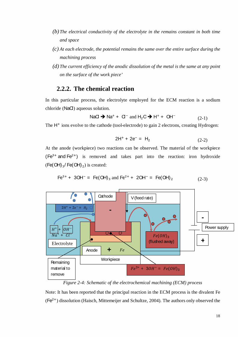
18
(b) The electrical conductivity of the electrolyte in the remains constant in both time
and space (c) At each electrode, the potential remains the same over the entire surface during the
machining process (d) The current efficiency of the anodic dissolution of the metal is the same at any point
on the surface of the work piece’
2.2.2. The chemical reaction
In this particular process, the electrolyte employed for the ECM reaction is a sodium
chloride (NaCl) aqueous solution.
NaCl Na + Cl and H O H + OH (2-1) The H ions evolve to the cathode (tool-electrode) to gain 2 electrons, creating Hydrogen:
2H + 2e = H (2-2)
At the anode (workpiece) two reactions can be observed. The material of the workpiece
(Fe and Fe ) is removed and takes part into the reaction: iron hydroxide
(Fe(OH) /Fe(OH) ) is created:
Fe + 3OH = Fe(OH) and Fe + 2OH = Fe(OH) (2-3)
Figure 2-4: Schematic of the electrochemical machining (ECM) process
Note: It has been reported that the principal reaction in the ECM process is the divalent Fe
(Fe ) dissolution (Haisch, Mittemeijer and Schultze, 2004). The authors only observed the
퐹푒3+ + 3푂퐻− = 퐹푒(푂퐻)3
퐻+ + 푂퐻− 푁푎+ + 퐶푙−
퐹푒
퐹푒(푂퐻)3 (flushed away)
2퐻+ + 2푒− = 퐻2
Cathode
Anode +
-
Workpiece
V (feed rate)
+
- Power supply
Remaining material to remove
Electrolyte

19
direct oxidation to Fe at high current efficiencies (η ≈ 100%). Figure 2-4 illustrates the
process.
The standard electrode potential for the reaction: Fe + 2e = Fe is E = −0.44V vs.
a standard hydrogen electrode (SHE).
According to the Nernst equation, the potential required to activate the above reaction is:
E . = E −R T2F ln(c ) (2-4)
Where R is the gas constant, T is the temperature (in K), c is the concentration of ion
Fe in the solution and F is the Faraday constant.
However, E . is also influenced by the pH. According to an electrochemistry course
(EPFL, 2011),
K =a a
a ( )≈ 10
c(a ) (2-5)
Where a , a and a ( ) are the activities of the different chemical species in the
electrolyte. a is the activity of the ion H in the solution.
With c = 0.01M and at pH = 7.45, K = 10 .
At 25°C (298.15K), = 2,5693.10
E . = E −R T2F ln(c ) = E −
R T2F ln(K . 10 . (a ) )
= −0.06 − 0.059pH
(2-6)
E . = −0.06 − 0.059pH
From the above equation it can be concluded that the activating potential of the dissolution
reaction also depends on the pH of the solution (EPFL, 2011).
2.2.3. The material removal rate (MRR)
2.2.3.1. MRR for pure materials (non-alloy)
The material removal rate (MRR) corresponds to the amount of metal removed per time unit
during the machining process. It is governed by Faraday’s law stating that the ‘amount of
removed material is proportional to the amount of charge (Q)’.

20
Moreover, the amount of material removed m during a time t depends on the
electrochemical equivalence (ECE) which is the ratio of the atomic weight A and the
valence z (McGeough, 1974). This relation is expressed by:
m = ηQ. AF. z = η. k. Q = η. k. I. t (2-7)
where
F is the Faraday’s Constant (F = 96500 C)
I is the current
t is the time
Q is the charge (Q = I. t).
η is the current efficiency (in %) defined as.
η = current responsible for metal dissolution
total current (I)
k = is a constant and it is specific to the material.
Expressing the dissolved mass dm in terms of removed material thickness dh over a time dt
and across a surface dS, the following expression can be obtained:
dm = ρ. dh . dS (2-8)
Where ρ is the density of the material of the anode (workpiece).
Furthermore, it is known that dm = η. k. I. dt = η. k. dQ so ρ. dh. dS = η. k. I. dt
So it can be deduced that:
dh = ηk I. dtρ. dS = K ×
IdS × dt = K . ia. dt (2-9)
Where
K = η is the coefficient of electrochemical machinability
i = I
dS is the current density at the surface of the anode
Finally the following equation is obtained:
MRR = mtρ =
Vt = η
Itktρ = η
Ikρ = I × K (2-10)
However, the previous formula is only working when one particular type of metal is
dissolved during the reaction. Since most of the manufacturing applications use alloys, it is
needed to go further in the development of this expression.

21
2.2.3.2. MRR for alloys in ECM
The formula to calculate the MRR for alloys in ECM is different: the atomic weight A
becomes A , the valence z becomes z and the mass fraction α is introduced. The index
i designates a specific metal that is a component of the alloy to dissolve.
For a volume V removed by passing a current I over a period of time t, the following
equation can be posed (ρ is the density of the alloy and m is the mass of one specific metal
of the alloy):
m = V ρα (2-11)
It is known that m = = Q k ; so Q = where Q is the amount of charge of
one specific metal of the alloy.
All the Q ′s are summed to obtain the total charge in the system:
Q = ∑Q = V ρ ∑( ) = ηIt (2-12)
Finally:
MRR = V
t = ηIρ ×
1∑(αk )
= I. K (2-13)
Where K is the coefficient of electrochemical machinability of the alloy.
2.3. Machining process
2.3.1. Review and analysis of the ECM and µECM machines available on the market
Most of the commercially available machines are ECM sinking machines and micro features
are made by copying the shape of the tool-electrode. ECM manufacturers are ‘Winbro
Group’ who offer stem drilling machines and die sinking machines (Winbro Group
Technologies, 2012), EMAG also offer die sinking ECM machines (EMAG GmbH, 2014)
and pECM systems (pECM Systems, 2014) provides the European market with a range of
ECM sinking machines from Russia (‘ET’ series manufactured by Indec (Indec, 2014)).
There is no great deal of µECM machines on the market. The literature review reported two
purpose-built machines able to perform µECM milling using simple shaped electrodes. The
first one has been developed by ECMTEC (ECMTEC GmbH, 2012) (now part of EMAG

22
GmbH) and is commercially available in table-top and standard models (EMAG, 2012). The
second machine has been reported in China and is a table-top machine developed for
research purposes (Wang et al., 2010). This machine is able to perform on-line tool
fabrication by Block Electrical Discharge Grinding (BEDG), whereas the EMAG machine
does not seem to have this capability for electrode preparation. Such machines are usually
developed and used in laboratory conditions mainly for research purposes and the available
documentation regarding them is very limited.
Sequential on-line tool machining followed by workpiece machining has been reported in
laboratory experiments but it seems that none of the commercially available machines have
the capability to perform it (Zhang, Wang, Chen and Mao, 2011). The reported work used
two different electrolytes: KOH to fabricate the tool and then HCl to machine the workpiece.
Having to manage two different electrolytes is a big constraint in the design of a machine
for industrial applications because the system has to be rinsed and different tanks must be
used to avoid contamination.
Usually when a new technology appears, people use and adapt existing machines for the
needs of the new technology. In this case the first attempts were to adapt EDM machines
for the purpose of the ECM technology. A difference should be made between the
development of simple die sinking machine (Figure 2-5) utilizing classical ECM removal
mechanism and machines developed which can be used to work in writing mode (µECM
milling) (Kirchner, Cagnon, Schuster and Ertl, 2001; Kim, Ryu, Choi and Chu, 2005b;
Kozak, Rajurkar and Makkar, 2004b; Liu, Zhu and Zhu, 2012). Die sinking ECM machines
use pre-shaped cathode electrodes and create the needed workpiece shape by copying the
shape of the cathode electrode onto the workpiece. Writing (or µECM milling) mode is a
term used to describe machining of complex shape features using tool-electrode with a
simple shape (i.e. cylindrical) and in this case the final shape of the machined feature is
created by consecutive movements of the simple-shaped electrode (Kozak, Gulbinowicz
and Gulbinowicz, 2008).

23
Figure 2-5: Typical ECM machine from Indec. Die sinking only. Source: http://www.indec-ecm.com/en/equipment/ET500/
2.3.2. Design requirements and constraints for µECM systems
2.3.2.1. Ultra-precision motion for tool-positioning
The accuracy required for the machine is directly linked to the accuracy required for the
final product. In µECM, it is usually required to maintain a gap smaller than 10µm during
machining (Cagnon et al., 2003; Schuster et al., 2000; Yong, Yunfei, Guang and
Liangqiang, 2003). Therefore the resolution of the machine movement should be a fraction
of that gap. Some developers in µECM even consider maintaining a gap size ranging from
1 to 5µm (Kirchner et al., 2001; Choi et al., 2013), the resolution of the machine movement
would be expected to be better than 100nm or less.
Huo et al. reported that the use of a closed frame mechanical structure provided better
stiffness (Figure 2-6) (Huo, Cheng and Wardle, 2010b). Their work provided a ‘bench-mark
and systematic methodology for designing bench-top ultra-precision machines, especially
those using direct-drive linear motors combined with aerostatic bearings’. This
methodology can therefore be used to satisfy the ultra-precision needs of the µECM
technology.

24
Figure 2-6: Two typical machine configurations and their coordinate definitions. (a) Open frame, (b) closed frame, (c) Structural loop stiffness calculated for both configurations
2.3.2.1. High dynamics and frictionless motion
The dynamics of the main axes (usually Z especially for die sinking operations) should be
very high in order not to damage the electrode when a short circuit occurs and to save
machining time when retracting and approaching the workpiece again (gap reset) (Yong et
al., 2003; Bhattacharyya and Munda, 2003). A 50ms reaction time of the mechanical
structure for the corresponding axes (usually Z) is a good example. In order to have high
dynamics and precise motion, the machine design should be based on the use of frictionless
slides like air-bearing stages (Luo, Cheng, Webb and Wardle, 2005; Wardle et al., 2010).
Counterweights and frictionless pressurized air cylinders can be used to support the weight
of the slides in order to improve the mechanical dynamics of the system (usually for the Z
axis). Air cylinders shall also have mounted brakes on them in order to prevent the supported
slides from being damaged in case of a pressure drop (Huo, Cheng and Wardle, 2010b).
The averaging effect of the air film on local surface errors allows the air-bearings to have
higher precision and better repeatability of motion compared to slide bearings or roller
bearings with mechanical contact between elements (Gao et al., 2006).
2.3.2.2. Workpiece clamping and tool holder constraints
Electrical and chemical constraints are also applied to the jigs and fixtures holding the
workpiece and the cathode electrode. During machining there is no physical contact between
the cathode and the anode and therefore there is no stress involved in the machining process
apart from the electrolyte flow causing some pressure onto the both electrodes.
For the workpiece, apart from removing the 6 degrees of freedom in an appropriate way for
the achieved dimensions and applying a small clamping force, the fixture should be able to

25
provide electrical contact which would preferably not to be exposed to the electrolyte flow.
This is needed to avoid the corrosion of the contact point and to make sure that the electrical
affinity of metals will not cause problems with the current flow.
The cathode electrode should have a reliable electrical contact with the power supply and it
should allow the flushing of the electrolyte through the cathode (hollow in that case) even
with a small diameter cathode. In some cases the electrolyte pressure may reach very high
values such as 70-100 bar if the diameter of the cathode electrode goes down to 80-100µm
diameter in order to have sufficient electrolyte flow. For smaller diameter electrodes, side
flushing is the only solution. Rotating cathodes should help the renewal of the electrolyte in
the working zone which is highly desirable for the efficiency and accuracy of the process.
The effect of the rotating tool on the electrolyte flushing could be enhanced using helical or
semi-cylindrical tools (Zhang et al., 2007; Tsui, Hung, You and Yan, 2008).
The development of spindles capable of precision rotation and able to transmit the high
frequency current pulses with minimized RF emissions is another challenge in order to
complete the design of a µECM machine.
2.3.3. Process monitoring and control
Usually, in order to be able to control a process, the variation of a reliable parameter has to
be measured and has to be significant enough in order to give a good representation of the
current state of the process. The control of the µECM and ECM processes mainly refers to
a constant adjustment of the process parameters in order to achieve better accuracy,
productivity and prevent from occurrence of electrical discharges (sparks). It ‘has been one
of the main goals of ECM machine manufacturers and user industries such as turbine
manufacturers’ (Rajurkar et al., 1995).
The control system of a PECM (µECM) machine is complex and is made of several
subsystems controlling different machining parameters: the interelectrode gap, electrolyte
flow, the voltage pulses and the temperature. The role of the electrolyte control subsystem
is to maintain the electrolyte properties and the flow rate at the inlet of the interelectrode
gap within a specified range.

26
2.3.3.1. Interelectrode gap control and optimization algorithms
Despite the progress made in Micro-ECM and PECM over the last 20 years, the
controllability and monitoring of the Interelectrode gap (IEG) in the process is still a big
issue. During the machining process, the motion control logic mainly depends on the
variation of the interelectrode gap size. The dimension of this gap can vary from a few µm
to 100µm depending on the application and has a dramatic influence on the machining
accuracy. When drilling micro-holes, the feed rate of the tool-electrode should match the
material removal rate of the process to maintain the gap size and reduce the chances for
short circuits to occur (Mithu, Fantoni, Ciampi and Santochi, 2012). The interelectrode gap
(IEG) is very hard to control because it cannot be measured directly.
The different issues influencing the IEG size that can be met during an ECM or PECM
process have been summarized as follows (Wei, 1994; Kozak, Rajurkar and Makkar,
2004a):
1. Variation of the electrical conductivity in the inter-electrode gap caused by the
appearance of bubbles in the electrolyte. This variation engenders a variation of the
material removal rate (Shin, Kim and Chu, 2008)
2. Lack of understanding of the kinetics and stoichiometry of the anodic reactions,
causing indeterminacy in the reaction modes (and then in the valence and
electrochemical equivalent);
3. Difficulty in determining anodic overpotential changes;
4. Variation in local anodic current efficiency;
5. Complexity of the involved mass and energy transport conditions in the gap;
6. Non-uniformity in the distribution of the electric field in the gap region;
7. Presence of stray current lines;
By using the eddy current technique, under specified frequencies, Bignon et al. have created
a measurement method of the IEG (Bignon, Bédrin and Weill, 1982). The authors claimed
that they could correct the deviations of the IEG from the normal gap value, by adjusting
one or several machining parameters (voltage, feed rate) and also claimed that this gave a
better reproducibility of machined shapes. However, this control approach has only been
applied to ECM and not to the PECM or µECM processes.

27
In 1984, Meijer et al. explained that ‘due to the non-linearity of the process a detail transfer
function, which is helpful in linear cases, cannot be used’ (Meijer and Veringa, 1984). The
process can however be linearized around a specific point but this generates approximations
error. In most cases binary logic control systems were used to control the interelectrode gap.
Based on the mathematical model of the interelectrode gap variation, Rajurkar et al.
simulated a gap control approach using state space representation (Rajurkar, Schnacker and
Packard, 1988). Nevertheless, no results were presented in their paper and no other work
using this method has been reported later. The validity of this approach regarding the µECM
process has therefore to be exploited further.
In 1996, Wei et al. proved that the current response of the PECM to a pulsed voltage could
be used as a sensing parameter to evaluate the interelectrode gap (Wei, Rajurkar and
Talpallikar, 1996). It was concluded that it is therefore possible to conceive an online gap
measurement system that can be used to control this parameter in real-time - which
confirmed the statements from (Rajurkar et al., 1995). This technique was used by Schuster
et al. who monitored the distance between the tool and workpiece by measuring the current
flowing through the cell (Schuster et al., 2000).
In 2000, De Silva et al. worked with Philips to model the process characteristics and increase
the dimensional control of the process (De Silva, Altena and McGeough, 2000). The
developed model managed to give a dimensional accuracy better than 5µm and a surface
finish better than Ra 0.03µm. The use of shorter pulses to reduce the size of the side gap
(Shin, Kim and Chu, 2008) – especially for non-side-insulated tools – is also recommended
to avoid taper-shaped holes (Fan and Hourng, 2011).
Yong et al. developed a control system based on the measurement of the current passing
through the system (Yong et al., 2003). To be able to control the gap during the machining
process, they moved the tool towards the workpiece until a ‘current jump-up’ and then
retracted the tool by a few µm (Figure 2-7).
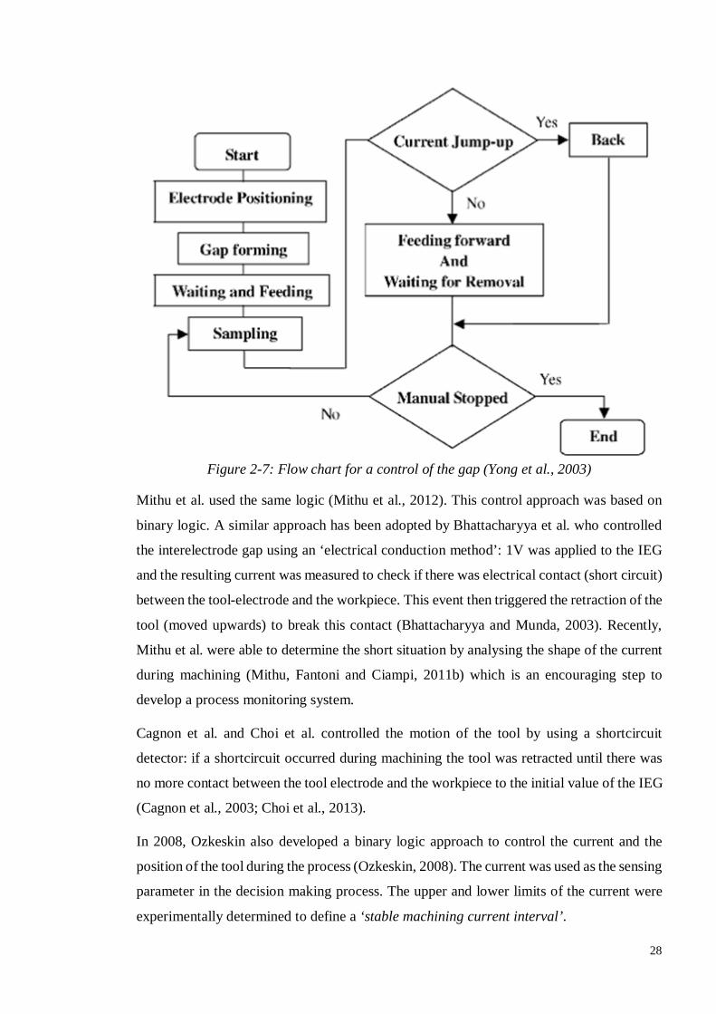
28
Figure 2-7: Flow chart for a control of the gap (Yong et al., 2003)
Mithu et al. used the same logic (Mithu et al., 2012). This control approach was based on
binary logic. A similar approach has been adopted by Bhattacharyya et al. who controlled
the interelectrode gap using an ‘electrical conduction method’: 1V was applied to the IEG
and the resulting current was measured to check if there was electrical contact (short circuit)
between the tool-electrode and the workpiece. This event then triggered the retraction of the
tool (moved upwards) to break this contact (Bhattacharyya and Munda, 2003). Recently,
Mithu et al. were able to determine the short situation by analysing the shape of the current
during machining (Mithu, Fantoni and Ciampi, 2011b) which is an encouraging step to
develop a process monitoring system.
Cagnon et al. and Choi et al. controlled the motion of the tool by using a shortcircuit
detector: if a shortcircuit occurred during machining the tool was retracted until there was
no more contact between the tool electrode and the workpiece to the initial value of the IEG
(Cagnon et al., 2003; Choi et al., 2013).
In 2008, Ozkeskin also developed a binary logic approach to control the current and the
position of the tool during the process (Ozkeskin, 2008). The current was used as the sensing
parameter in the decision making process. The upper and lower limits of the current were
experimentally determined to define a ‘stable machining current interval’.
29
In 2002, Clifton et al. demonstrated that the measurement of the IEG using ultrasonic waves
can also be successfully applied to control the interelectrode gap (Clifton, Mount, Alder and
Jardine, 2002). However the gap measured in the experiment were not smaller than 400µm
which makes this method not very suitable for µECM. Wei et al. also proposed and patented
a method to monitor electrochemical machining by generating ultrasonic waves towards the
workpiece thanks to two ultrasonic transducers and then measuring arrival times (Wei, Li
and Lamphere, 2005). Although, the smallest gap that could be measured using this
technique is not mentioned in the patent. Muir et al. also reported the development of a
similar system to measure the interelectrode gap (Muir et al., 2007). The dimensions of the
gap did not correspond to the case of µECM: the machining area was around 600mm² and
the initial gap was 1mm, which were much greater than the IEGs used in µECM.
In 2004, Schuster et al. proposed a patented ‘method for electrochemically processing
material’ (Schuster and Kirchner, 2004). They also presented a way to control the
interelectrode gap within a 10µm range. The current peaks were measured via a current peak
detector and their values were compared with the desired value. The output of the
comparator was passed through a low pass filter (integrator) and a downstream amplifier.
This amplifier controlled an electromagnetic mechanism that had a 10µm travel distance.
The position of the workpiece was then adjusted with respect to the measured current peaks.
The authors claimed that the gap was ‘sufficiently small to obtain the desired local
resolution’ and ‘sufficiently high to avoid short circuits’. However, no specific distances
were mentioned.
In order to monitor the gap size, Kim et al. (Kim et al., 2005a) measured the potential drop
between the tool and the workpiece (Figure 2-8). If the potential drop was equal to zero, this
meant a short circuit was detected. This potential drop can therefore be used to control the
feed rate of the tool electrode and also detect short circuits.

30
Figure 2-8: A system for µECM (Kim et al., 2005a)
Labib et al. pointed out the necessity for the controller to have decision making capabilities
(Labib et al., 2011). Since the PECM process is very hard to mathematically model,
conventional control approaches such as proportional-integral-derivative (PID) or state
space controllers are limited and based on the linearisation of the process function (and
therefore approximation). They observed that the occurrence of sparking was efficiently
prevented when fuzzy logic control (FLC) was applied to the ECM process and encouraged
further research to develop FLCs for the EMM process. Moreover, it is worth mentioning
that fuzzy logic was also used to control the process in EDM, Wire-EDM (Çaydaş, Hasçalık
and Ekici, 2009; Lin, Chung and Huang, 2001) and Electro-Chemical Discharge Machining
(ECDM) (Mediliyegedara, Silva, Harrison and McGeough, 2005; Skrabalak, Zybura-
Skrabalak and Ruszaj, 2004).
Labib et al. also suggested the association of FLC to another control method and claimed
that the FLC would bring ‘intelligent control’ to the process. They also mentioned that
investigation in the area of adaptive neuro-fuzzy inference system (ANFIS) would provide
the control system also with learning capabilities (Labib et al., 2011). The combination of
an active control loop with neural networks or optimisation algorithms seems very
promising as some authors have already used neural networks to tune the machining
parameters in ECM (Abuzied, 2012; Li and Ji, 2009; Asokan, Ravi Kumar, Jeyapaul and
Santhi, 2008; Zare Chavoshi, 2011). Recently, micro-herringbone grooves were machined
in hydrodynamics bearings using a simulation-assisted µECM process (Chang et al., 2011).
Fuzzy logic was also applied to control the gap during an ECM process using a 6D force
sensor while measuring the machining current (Yonghua and Kai, 2010).
Finally, in 2010 a CNC system was developed for µECM using a soft-CNC architecture
based on RT-Linux. This system used a real-time module to handle the motion, short-circuit

31
detection (the detection signal was coming from the pulse generator) and gap adjustment
aspects (Wang et al., 2010). The authors managed to mill an hexagonal star and micro-
stepped cavities at a feed rate of 6µm/min using G code generated from a standard
CAD/CAM software.
The majority of the authors consider that the most reliable sensing parameter to control the
IEG is the current (Yong et al., 2003; Schuster and Kirchner, 2004; Ozkeskin, 2008;
Bhattacharyya and Munda, 2003; Mithu et al., 2012; Cagnon et al., 2003), so a good
relationship between the current and the gap size must be defined. The only way to answer
this demand is to create electrical model(s) of the interelectrode gap.
2.3.3.2. The electrical double layer (EDL) effect in µECM
The electrical double layer can be considered as an ‘electrical barrier’ located between the
metal and the solution in which it is submerged. More precisely, it is a potential difference
that is established by ‘the transfer of the metal ions to the solution’ and ‘the discharge on
the ions from the solution’. When this phenomenon reaches an equilibrium potential
difference, a layer of metallic ions (+ at the anode) - whose charge is equal and opposite to
those in the solution (-) - is formed at the metal-solution interface: the EDL is then fully
established (McGeough, 1974). In PECM and ECM the electrical model of the inter-
electrode gap is a variable resistance. However, in µPECM the effect of the electrical double
layer is significant enough not to be neglected.
The EDL has several characteristic regions: (A) the Helmholtz double layer and (B) the
Gouy-Chapman layer. Helmoltz highlighted that the double layer (A) could be treated as a
capacitor since it consists of 2 plans parallel to each other and having opposite charges. On
the other hand, over the Gouy-Chapman layer (B) – also called ‘diffuse layer’ –, the
potential decreases exponentially when the distance from the metal surface increases: the
potential drop over that layer is therefore non-linear. These layers can be represented the
following way (Figure 2-9):

32
Figure 2-9: Representation of the electrical double layer and its different characteristics
(Spieser, 2011)
These statements imply that in order to dissolve the metal in the solution, the energy
necessary for the ions to pass across the double layer has to be supplied (McGeough, 1974).
Fujii et al. analyzed the EDL in a NaCl aqueous solution (Fujii, Muramoto and Shimizu,
2010). They applied an increasing voltage to an electrochemical cell with 2 electrodes made
of the same material (2 experiments were conducted: one with SUS304 stainless steel
electrodes and the other with gold electrodes). The electrodes were both submerged in a
5wt% NaCl solution. During the experiment an increase of the double layer capacitance has
been observed: when the DC voltage was 0.3~0.5V the measured capacitance was about
10.6μF and for 1V, the capacitance was 34.6μF (Figure 2-10). They therefore concluded
that the double layer capacitance was a function of the charging voltage.
Figure 2-10: The capacitance as a function of the charging voltage. The error bar shows maximum and minimum values in 3 measurements. (Fujii, Muramoto and Shimizu, 2010)
Metal
+
+
+
+
+
+
Solution
-
-
-
-
-
-
-
-
-
-
-
(A) Helmoltz double layer
(B) Gouy-Chapman layer
Bulk electrolyte

33
Furthermore, they noticed that: ‘Current started to flow through the cell at 0.6V and 1.1V
for the SUS304 steel electrodes and the gold electrodes respectively’. Fujii et al. explained
the increase of the capacitance by the fact that when the voltage gets closer to the activating
potential of the corrosion reaction, the density of ions in the electrical double layer increases:
‘the distance between the layers of the EDL decreases and the number of ions participating
in the EDL increases’.
Furthermore, Schuster et al. claimed that the activating potential over the double layer was
proportional to the electrolyte resistivity (Schuster and Kirchner, 2004).
It can be seen that the behaviour of the electrical double layer is very complex: its
capacitance depends on the concentration of the electrolyte, the chemical species (type of
ions) in the solution, on the applied voltage and on the material of the electrodes. The
electrolyte has therefore to be chosen carefully according to properties of the material of the
workpiece (Spieser, 2011).
In 2000, Schuster et al. experimented PECM with ultra-short pulses by taking into account
the effect of the electrical double layer (Schuster et al., 2000; Kirchner et al., 2001). Studies
showed that a capacitor was a suitable representation of the electrical double layer in this
process (Schuster et al., 2000; Ahn, Ryu, Choi and Chu, 2004). The electrical model of the
gap that they used is presented on Figure 2-11.
Figure 2-11: Scheme of an electrical cell, the double layer capacity (퐶 ) is
charged via the electrolyte resistance (Schuster et al., 2000)
Kozak (Kozak, Gulbinowicz and Gulbinowicz, 2008) and Marla et al. (Marla, Joshi and
Mitra, 2008) improved this model by adding non-linear resistors (r and r ) in parallel with
the electrical double layers (Figure 2-12).

34
Figure 2-12: Electrical model of the interelectrode gap proposed for the
µECM process(Kozak, Gulbinowicz and Gulbinowicz, 2008)
They claimed that the current going through the double layer was actually the sum of 2
different currents (Figure 2-13):
The charging current: It is the current that flows through the double layer when the latter
is getting charged.
The faradaic current: It is the current that causes the dissolution of the material when
the electrical double layer is fully charged.
Figure 2-13: Charging and discharging waveforms during µECM machining
(Mithu, Fantoni and Ciampi, 2011a)
It can be said that the current representing the gap size is the faradaic current because it only
starts flowing through the cell when the electrical double layer is fully charged, and is
therefore strongly related to the interelectrode gap resistance. The use of this model has been
reported by other authors (Mithu, Fantoni and Ciampi, 2011a; Fan, Hourng and Lin, 2012;
Ahn et al., 2004).
To increase the amount of faradaic current contained in each pulse, Kozak et al. made µECM
trials by combining a DC voltage source and a pulsed voltage. The role of the DC voltage

35
was to polarise the electrical double layer to make sure that it would never discharge, then
the voltage pulses would remove material more efficiently and at the same time, the tool
would be protected from corrosion. The DC voltage was therefore relatively low and below
the activating potential of the electrochemical reaction (Kozak, Rajurkar and Makkar,
2004b).
The current is mainly influenced by the conductivity of the electrolyte and the gap size.
However, the conductivity of the electrolyte is influenced by several parameters including
the ionic concentration (i.e. pH, Cl , NO ) and the temperature.
Therefore, if the current is used as a sensing parameter, the properties of the electrolyte have
to be carefully maintained constant within the IEG, otherwise the relationship between the
measured current and the gap size changes.
In order to have a more accurate representation of the gap, the side walls of the cathode (tool
electrode) should be insulated to prevent the current from flowing through them: only the
current flowing through the front face of the cathode can be used to indirectly measure the
IEG size unless a very complicated algorithm is created to compensate for the change of the
active zone on the cathode electrode.
2.3.3.3. Control of the voltage at the electrodes
In some papers, a polarisation of the workpiece and the tool-electrode have been reported
(Trimmer et al., 2003; Zemann, Reiss, Schörghofer and Bleicher, 2012; Schuster et al.,
2000; Yang, Park and Chu, 2009; Park, Kim and Chu, 2006; Kirchner et al., 2001; Shin,
Kim and Chu, 2008). Researchers employed a low-frequency bipotentiostat which was
maintaining independently - with the aid of a platinum counterelectrode - specified base
values of potentials of the tool and workpiece relative to a reference electrode (Figure 2-14).
The potentials were selected so as to prevent the corrosion of the electrodes and to prevent
the formation of an oxide layer on the surface of the workpiece (Park, Kim and Chu, 2006;
Schuster et al., 2000). They applied a train of voltage pulses (pulse-on time 50 ns, pulse-off
time 500 ns) coming from a pulse generator to the workpiece. Such short pulses did not
interfere with the potentiostat operation, so the generator could polarize the workpiece
precisely in the area to be dissolved (Davydov, Volgin and Lyubimov, 2004; Schuster et al.,
2000).
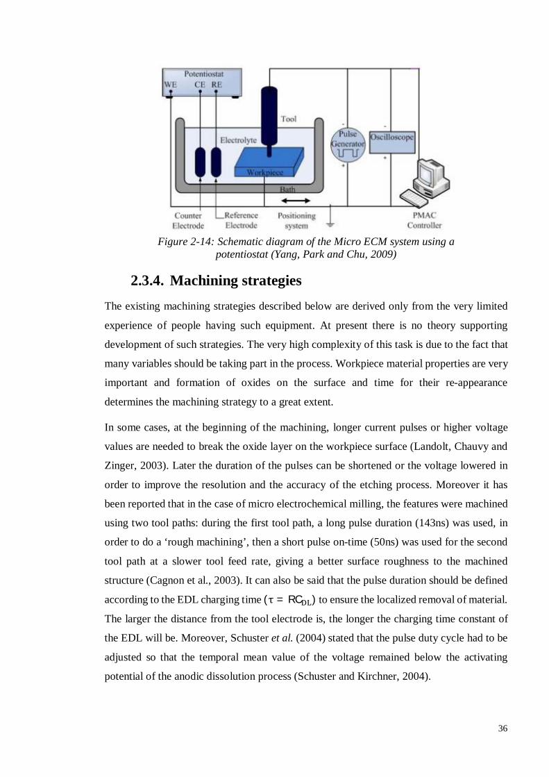
36
Figure 2-14: Schematic diagram of the Micro ECM system using a
potentiostat (Yang, Park and Chu, 2009)
2.3.4. Machining strategies The existing machining strategies described below are derived only from the very limited
experience of people having such equipment. At present there is no theory supporting
development of such strategies. The very high complexity of this task is due to the fact that
many variables should be taking part in the process. Workpiece material properties are very
important and formation of oxides on the surface and time for their re-appearance
determines the machining strategy to a great extent.
In some cases, at the beginning of the machining, longer current pulses or higher voltage
values are needed to break the oxide layer on the workpiece surface (Landolt, Chauvy and
Zinger, 2003). Later the duration of the pulses can be shortened or the voltage lowered in
order to improve the resolution and the accuracy of the etching process. Moreover it has
been reported that in the case of micro electrochemical milling, the features were machined
using two tool paths: during the first tool path, a long pulse duration (143ns) was used, in
order to do a ‘rough machining’, then a short pulse on-time (50ns) was used for the second
tool path at a slower tool feed rate, giving a better surface roughness to the machined
structure (Cagnon et al., 2003). It can also be said that the pulse duration should be defined
according to the EDL charging time (τ = RC ) to ensure the localized removal of material.
The larger the distance from the tool electrode is, the longer the charging time constant of
the EDL will be. Moreover, Schuster et al. (2004) stated that the pulse duty cycle had to be
adjusted so that the temporal mean value of the voltage remained below the activating
potential of the anodic dissolution process (Schuster and Kirchner, 2004).
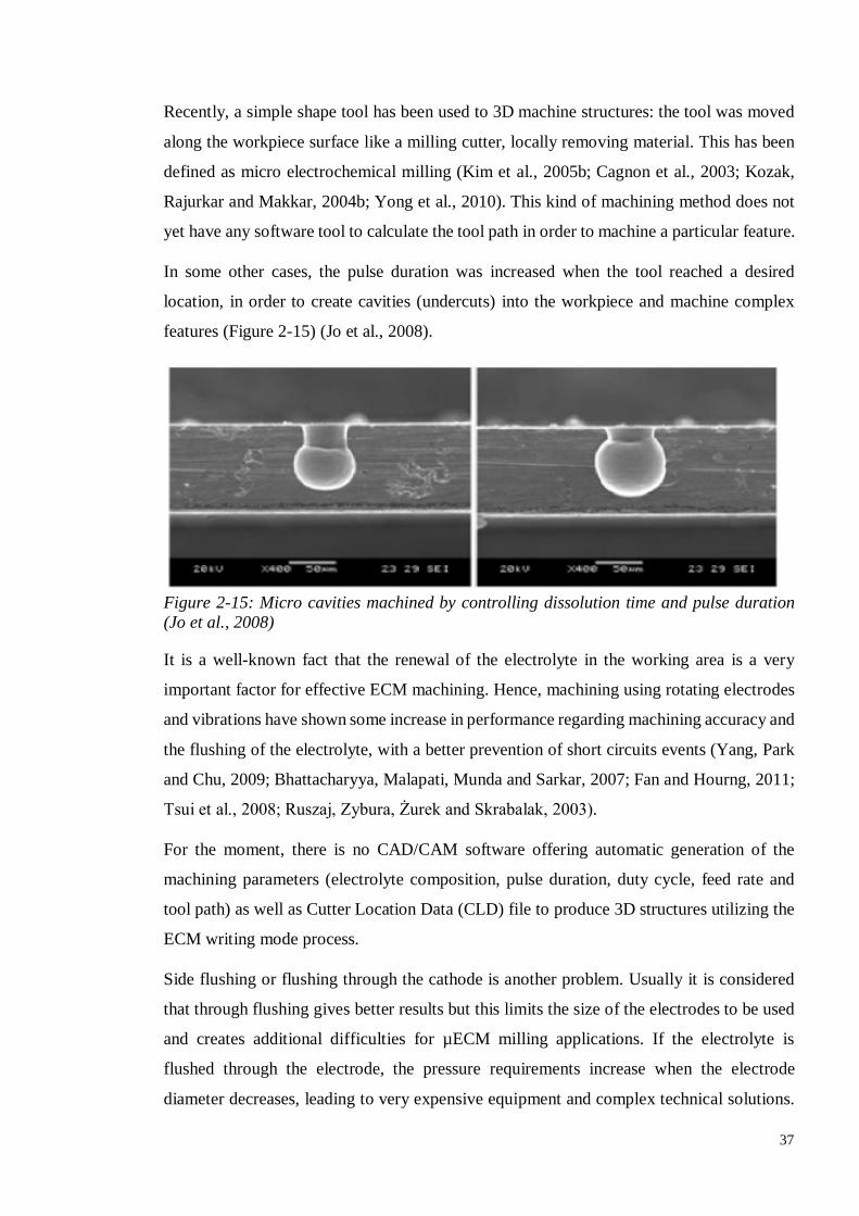
37
Recently, a simple shape tool has been used to 3D machine structures: the tool was moved
along the workpiece surface like a milling cutter, locally removing material. This has been
defined as micro electrochemical milling (Kim et al., 2005b; Cagnon et al., 2003; Kozak,
Rajurkar and Makkar, 2004b; Yong et al., 2010). This kind of machining method does not
yet have any software tool to calculate the tool path in order to machine a particular feature.
In some other cases, the pulse duration was increased when the tool reached a desired
location, in order to create cavities (undercuts) into the workpiece and machine complex
features (Figure 2-15) (Jo et al., 2008).
Figure 2-15: Micro cavities machined by controlling dissolution time and pulse duration (Jo et al., 2008)
It is a well-known fact that the renewal of the electrolyte in the working area is a very
important factor for effective ECM machining. Hence, machining using rotating electrodes
and vibrations have shown some increase in performance regarding machining accuracy and
the flushing of the electrolyte, with a better prevention of short circuits events (Yang, Park
and Chu, 2009; Bhattacharyya, Malapati, Munda and Sarkar, 2007; Fan and Hourng, 2011;
Tsui et al., 2008; Ruszaj, Zybura, Żurek and Skrabalak, 2003).
For the moment, there is no CAD/CAM software offering automatic generation of the
machining parameters (electrolyte composition, pulse duration, duty cycle, feed rate and
tool path) as well as Cutter Location Data (CLD) file to produce 3D structures utilizing the
ECM writing mode process.
Side flushing or flushing through the cathode is another problem. Usually it is considered
that through flushing gives better results but this limits the size of the electrodes to be used
and creates additional difficulties for µECM milling applications. If the electrolyte is
flushed through the electrode, the pressure requirements increase when the electrode
diameter decreases, leading to very expensive equipment and complex technical solutions.

38
Moreover, the gap size between the electrodes must be big enough to allow the electrolyte
to circulate.
Side flushing does not require expensive equipment, but the electrolyte flow might apply a
lateral force which could bend the tool and disturb the machining process especially when
high aspect ratio is required.
2.4. Pulse power supply unit (PSU) considerations In µECM, a special PSU is needed. It should be able to apply pulses with the following
characteristics:
- Pulse amplitude : 1-10V (Bhattacharyya and Munda, 2003)
- Current : up to 5A (dependant of the cathode working area)
- Frequency : ranging from 1kHz up to 5MHz
This kind of device is hard to design mainly because it requires the MOSFETs to be
switched at a very high frequency. Indeed, most of the silicon based power transistors
commercially available are designed to work at a maximum switching frequency of 1 MHz
and are limited by their turn-on and turn-off times. To make a MOSFET turn on in a few
nanoseconds, a high current pulse (of several amps) has to be applied to quickly charge the
capacitor at its gate (Oh, 2000; Balogh, 2001). Therefore in most cases a special gate driver
needs to be developed (Tang and Burkhart, 2009). Although the design of single switch
pulse generators has been reported (use of a RF MOSFET (Campbell, Harper, Natham,
Vinodhkumar, Xiao and Sundararajan, 2008) and use of a thyristor (Bhattacharyya and
Munda, 2003)), most of the µECM power supplies found in the litterature have a half bridge
configuration (Zhang et al., 2009; Burkert, Schulze, Gmelin and Leone, 2009). The low side
switch applies the voltage pulse to the gap when it is closed (pulse on-time), and the high
side switch shorts the gap during the pulse off-time. Driving the high side switch at very
high frequencies is another issue, since the conventional high side gate drive technique using
a bootstrap diode and a bootstrap capacitor cannot be used (because of the relatively long
charging/discharging time of the bootstrap capacitor). A solution to this problem is to
completely isolate the high side using an isolated DC/DC converter. The DC/DC converter
should be designed to supply the driver with enough current to drive the MOSFET at the
required frequency.
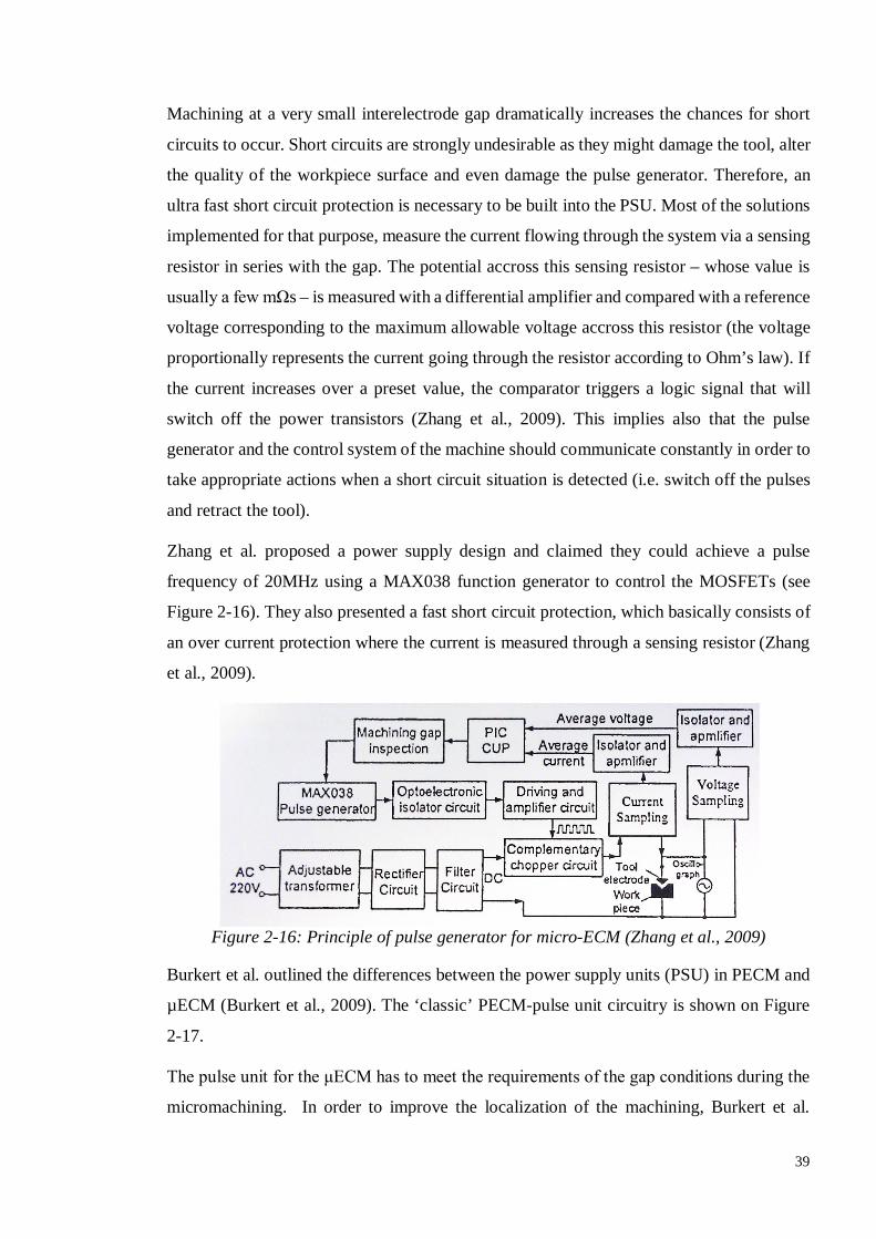
39
Machining at a very small interelectrode gap dramatically increases the chances for short
circuits to occur. Short circuits are strongly undesirable as they might damage the tool, alter
the quality of the workpiece surface and even damage the pulse generator. Therefore, an
ultra fast short circuit protection is necessary to be built into the PSU. Most of the solutions
implemented for that purpose, measure the current flowing through the system via a sensing
resistor in series with the gap. The potential accross this sensing resistor – whose value is
usually a few mΩs – is measured with a differential amplifier and compared with a reference
voltage corresponding to the maximum allowable voltage accross this resistor (the voltage
proportionally represents the current going through the resistor according to Ohm’s law). If
the current increases over a preset value, the comparator triggers a logic signal that will
switch off the power transistors (Zhang et al., 2009). This implies also that the pulse
generator and the control system of the machine should communicate constantly in order to
take appropriate actions when a short circuit situation is detected (i.e. switch off the pulses
and retract the tool).
Zhang et al. proposed a power supply design and claimed they could achieve a pulse
frequency of 20MHz using a MAX038 function generator to control the MOSFETs (see
Figure 2-16). They also presented a fast short circuit protection, which basically consists of
an over current protection where the current is measured through a sensing resistor (Zhang
et al., 2009).
Figure 2-16: Principle of pulse generator for micro-ECM (Zhang et al., 2009)
Burkert et al. outlined the differences between the power supply units (PSU) in PECM and
µECM (Burkert et al., 2009). The ‘classic’ PECM-pulse unit circuitry is shown on Figure
2-17.
The pulse unit for the μECM has to meet the requirements of the gap conditions during the
micromachining. In order to improve the localization of the machining, Burkert et al.

40
claimed it is necessary to reload the double layer capacitances, which means both loading
and unloading them. They presented a bipolar PSU enabling to load/unload the electrical
double layer thanks to two power sources, as shown on Figure 2-18.
Figure 2-17: Basic circuitry of pulse-unit (PU) for PECM in connection with gap via feeder. Switches SW carry the rising current 푖 during the pulse on-time, diodes D carry the falling reverse-current 푖 at beginning of the pulse off-time. PU is connected to supply-unit PS on the left side. (Burkert et al., 2009)
Figure 2-18: Basic circuitry of simple μECM pulse-unit (PU) in push-pull topology with bipolar (two) power supply (PS) feeding. Switches SW may conduct in alternation for loading and reloading of the gap’s double layer capacitance. (Burkert et al., 2009)
The two supply voltages of the power supplies PS1 and PS2 are adjustable; the
unloading/loading of the double layer capacitances can therefore be controlled and hence
the current slope can be optimized for a more efficient metal dissolution. ‘In this respect,
the connecting of the gap to the necessary voltages takes place via the semiconductor
switches SW1 for the positive PS1, and SW2 for the negative PS2. The diodes D serve the
purpose of protecting the circuit.’ (Burkert et al., 2009).
A low cost power supply unit with satisfying performance will have to be developed in order
to make the µECM technology fulfill the needs of the industry. Lots of further research is

41
therefore needed in this particular area. Schulze et al. outlined the specifications of an
energy source that have to be developed in order to efficiently use ECM for micro-
machining (Schulze, Borkenhagen and Burkert, 2008).
Recent developments in Gallium Nitride (GaN) power transistors (such as the eGaN FET
from EPC Corporation) having a very high switching speed with a very small package
inductance and resistance should make the development of this kind of power supply more
feasible (Danilovic et al., 2011).
Since the pulses last about 20ns each, and that a very high current density is applied, an
innovative power supply unit (PSU) has to be developed. In µECM, the EDL
loading/unloading time can be controlled to improve anodic dissolution. For this reason, the
PSU circuitry for PECM is not the same as in µECM.
2.5. Electrode and workpiece preparation In µECM, the shape of the cathode electrode has a direct influence of the shape created on
the anode electrode. Therefore, the accuracy of the tool shape has a direct effect on the
workpiece accuracy (Bhattacharyya, Malapati and Munda, 2005). As mentioned before, the
cathode electrode does not wear during the machining process, so the electrode does not
have to be changed after the machining operation. It is also worth mentioning that the shape
of the tool tip has an influence on the machining performance (Swain, 2010; Liu, Zhu, Zeng
and Yu, 2011).
2.5.1. Tool design software Tool design software tool chains have been developed to help define the shapes and feature
sizes to be machined onto the cathode electrode for the desired application.
The methods and software that were used to design tools for ‘normal’ ECM and millisecond
range PECM (Kozak et al., 2000; Purcar, Bortels, Vandenbossche and Deconinck, 2004)
cannot be applied to the µECM because the effect of the electrical double layer is not
considered in the normal ECM simulation. All these simulation tools use analytical
numerical methods such as the boundary elements method (BEM) (Deconinck, 1992;
Pattavanitch, Hinduja and Atkinson, 2010; Narayanan, Hinduja and Noble, 1986), the finite
difference method (FDM) (Kozak, 2001) or the finite element method (FEM) (Jain and
Pandey, 1981) to map the current density over the cathode and workpiece surfaces according
to predefined parameters (electrolyte conductivity, geometrical configuration). The main

42
challenge is to take into account the variation of the electrical potential distribution (and
therefore, of the current density distribution) when material is removed: the distribution of
the electrical potential needs to be recalculated after each pulse. In most of the time, to
simplify the system, the electrical double layer capacitance and the conductivity of the
electrolyte within the IEG (depending on both temperature and electrolyte concentration)
are considered constant throughout the machining time (Kozak, Gulbinowicz and
Gulbinowicz, 2008; Marla, Joshi and Mitra, 2008). More recently, simulations have been
performed taking into account the temperature distribution in the IEG and its influence on
the shape evolution during machining (Deconinck, Van Damme and Deconinck, 2012a; b).
The current density is at its strongest value at the end surface of the electrode. However,
when the workpiece is machined the sidewalls of the electrode also have an influence on
the shaping process. In reality, µECM processes present a non-uniform current density
distribution along the surface of the workpiece (Kock, Kirchner and Schuster, 2003;
Floridor et al., 2004).
Kenney et al. and Chang et al. proposed simulation tools and procedures that could be used
for future cathode tool design and process parameter study for the EMM process (Kenney,
Hwang and Shin, 2004; Chang et al., 2011).
More recently, Hotoiu et al. have been working on the development of a software pack to
simulate the µECM process by taking into account the effect of the electrical double layer
(Hotoiu, Van Damme and Deconinck, 2011; Hotoiu et al., 2011; Van Damme et al., 2011).
2.5.2. Off-Machine electrode fabrication In cases of die sinking operation the cathode electrode has to be machined in advance and
there is a complex relationship between the shape of the final product and the shape of the
cathode electrode, as explained above. The shape of the tool electrode is usually complex
(Wang and Zhu, 2009; Trimmer et al., 2003). This process requires sometimes the
combination of different machining technologies (such as milling, EDM and followed by
electrochemical etching (Wang and Zhu, 2009)).
In these cases 3D micro features are machined on the cathode electrode which is then used
to create the features onto the anode workpiece (Figure 2-19) (Chang et al., 2011; Trimmer
et al., 2003).

43
Figure 2-19: Scanning electron micrographs (a) the tool; (b)
structure in Ni substrate (Trimmer et al., 2003)
To reduce the stray current, the sides of the tool can be insulated. When using insulated
tools, ‘the machining rate and the machining gap are uniform, regardless of the machining
depth’. Moreover, the taper shape of structures can be effectively prevented (Park, Kim and
Chu, 2006).’Insulated materials like SiC, 푆푖 푁 can be coated on the side wall of the
cathode by chemical vapour deposition (CVD) process.’ (Bhattacharyya and Munda, 2003;
Bhattacharyya, Malapati and Munda, 2005). A dual pole tool would also help achieving a
higher accuracy by making the current flow only through the front face of the electrode (Zhu
and Xu, 2002). In µECM, the use of acid-based electrolyte implies that the insulation
material should be resistant to corrosive chemicals. Jo et al. reported the use of ‘polystyrene
as an adhesive and tetrahydrofuran (THF) as a solvent’ to overcome corrosion problems
(Jo et al., 2008).
All the above recommendations require the cathode to be prepared off the machine.
Therefore - for such precise machining application - the clamping of the tool electrode is a
very delicate step at machine setup procedure.
2.5.3. On-Machine electrode preparation
In drilling and milling operations, the cathodes usually have a simple shape (cylindrical or
semi-cylindrical) and can be machined by electrochemical etching (Figure 2-20) (Zhang et
al., 2007, 2011; Lee, Baek and Cho, 2007; Mathew and Sundaram, 2012; Liu, Zhu and Zhu,
2012; Choi, Ryu, Choi and Chu, 2007) or in a manner similar to the Wire Electro-Discharge
Grinding devices (Figure 2-21) which allows to achieve very small sizes (diameters) (Yang,
Park and Chu, 2009; Huang, Huang and Yan, 2004).

44
Figure 2-20: 10 µm tungsten tool electrode machined using
electrochemical etching (Zhang et al., 2007)
Figure 2-21: Schematic diagrams of the tool electrode fabrication: (a) cylindrical tool and
(b) semi-cylindrical tool (Yang, Park and Chu, 2009)
The diagram in Figure 2-22 shows an example of a micro-tool being machined using
electrochemical etching (anodic dissolution of the tool with a DC current) followed by the
machining of the workpiece (anodic dissolution of the workpiece using the pulsed power
supply unit). One of the major benefits of the on-the-machine electrode preparation is that
the axis of rotation of the electrode and the electrode position and dimension(s) are known.
Figure 2-22: Schematic diagram of µECM sequentially: (a) micro-tool machining, (b)
micro-workpiece machining (Zhang et al., 2011)

45
Once the tool is ‘ground’ and the required size is achieved, it can be used in the
electrochemical micromachining process by reversing the polarity of the electrodes (Zhang
et al., 2011).
In analogy with the micro EDM process, block wire and disk electrodes can be used for the
on-the-machine electrode preparation (Pham et al., 2004).
Until now, no publications have been found to show which method of on-the-machine
electrode preparation would be the most suitable for the µECM process. However, the
modelling of the fabrication of micro tools using pulse electrochemical micromachining has
been reported recently (Mathew and Sundaram, 2012; Kamaraj and Sundaram, 2013). This
step is crucial in the development of the on-machine tool-electrode preparation and further
developments are very likely to be seen in the coming years.
2.5.4. Electrical connections Burkert et al. stated that one of the critical parameters of the µECM process circuitry is the
inductance of the cables connecting the PSU to the electrodes (Burkert et al., 2009). This
parasitic cable inductance increases the rise time of the voltage pulses especially for pulse
durations below 1µs. At high frequency, the impedance of the cable gets so big that only a
portion of the output power is delivered to the IEG and the pulses are distorted. The cabling
therefore limits the frequency at which machining can occur and problems have been
reported above 1MHz (Fan, Hourng and Lin, 2012). To solve this issue, special low
inductance cables should be used and their length must be minimised. The use of coaxial
cables to minimise cable inductance have also been reported (Park, Kim and Chu, 2006).
This would mean that the PSU has to ‘be positioned as close as possible at the gap
connection’ (Burkert et al., 2009). This task becomes even more difficult when additional
device like the described above on-the machine grinding device should be considered for
the wiring.
In µECM tool electrodes with simple shapes (cylindrical or semi-cylindrical) are used in
most cases. The electrical connection of the cathode is complex to achieve because the tool
is spinning: energy must be reliably transmitted to the rotating element (Zhang et al., 2009).
In the case of high frequency power supply and high current it is not suitable to use the
traditional carbon or silver brushes because the transmission of high current has a
detrimental effect on them and they do not work well at high frequency (parasitic

46
inductance). At the moment there is no good solution on the market such as a system
transmitting high frequency signals and high current to a spinning electrode and at the same
time to be located as close as possible to the IEG.
The electrical connection of the anode electrode (workpiece) is even more complicated and
important as few rules have to be followed:
Only the machined material has to be exposed to the electrolyte and the electrical
connection.
The cables should be special and with minimum length to minimize the inductance.
In the best case the working zone should be in a structure acting like a Faraday cage
to prevent RF emissions and reduce parasitic inductance.
In the case of on-the-machine electrode preparation the power supply should be able
to reverse the polarity of the pulses and the wiring should support this as well.
2.6. Measurement Measuring the workpiece position in the coordinate system of the machine, the electrode
dimensions, the achieved feature dimensions or the surface roughness of micro-features is
not an easy task. All measurements have to be performed on the machine, because any off-
machine measurement is linked with introducing more errors associated with removing and
re-setting up either of the tool-electrode or the workpiece or both. On-the-machine
measurement of the tool-electrode and feature dimensions is necessary in order to achieve
good accuracy in a µECM machining process. This is mainly due to the fact that removing
a machined part for measurement and resetting it up afterwards will create an error that will
severely affect the final accuracy of the machined features.
2.6.1. Measuring dimensions
At present there is no accurate way to predict the achieved dimensions with the µECM
process. There are not many machines available and all µECM machines are still in state
where these new features are under development. In analogy with the micro EDM process
where the electrode is used as a probe to perform measuring functions as well, in µECM
machines it will be not that easy to adopt the same approach.
In µECM machines, similarly to the micro-EDM machines, the two electrodes are
electrically insulated from each other. However regarding the micro-EDM process the

47
working medium used is dielectric which allows the use of the electrode for probing based
on electrical contact between the electrode and the surfaces from the workpiece.
Regarding µECM machines the working medium is electrically conductive and such
approach is not applicable unless further research and developments are done. At present
the approach is to remove all electrolyte from the electrode and the workpiece and to use
measuring cycles similar to the one used in micro-EDM machines based on the electrical
contact between the electrode and workpiece surfaces. The dimensions are calculated using
data from the encoders which register the exact moment of electrical contact, as suggested
by (Bhattacharyya and Munda, 2003). Measuring algorithms are well developed and used
for many years on coordinate-measuring machines (CMM) and all CNC-based machines
utilising measuring cycles.
Different researchers communicate that repeatability of the process is very high but a test
run is needed in order to establish the exact parameters of the process and to measure the
achieved dimensions. The dimensions and the corresponding accuracy are directly related
to the method used for achieving and maintaining the IEG. If the method of maintaining the
IEG is accurate and the IEG variation is small then the machining accuracy from the pulsed
µECM process is good.
2.6.2. Machine set-up
At present the development of µECM equipment is still at research level. Nearly all
machines use one pre-set cathode electrode for one specific operation. Therefore the setting
up of the machine will be considered only for one electrode which simplifies the machining
set up procedure. As for all setting up procedures for CNC machines, the setup includes:
Determining the position of the working coordinate system of the workpiece according
to the machine coordinate system;
Measuring the relative position of the cathode electrode according to the workpiece
coordinate system.
The setting up procedure in this case will involve also positioning of the electrode to the
IEG distance which has to be maintained during machining operation.
There are no reported machines with optical devices for setting up the position of the
workpiece and therefore the described above measuring capabilities of the machine will be
used to determine the position of the working coordinate system (workpiece coordinate

48
system) in the machine coordinate system and the position of the programmed point from
the cathode electrode in two dimensions length (usually in Z direction) and diameter
(usually X, Y direction).
To define the IEG, a similar approach is used. A small voltage is applied to the
electrochemical cell and the tool is being moved towards the workpiece until a short circuit
is detected. Then the tool is very slowly retracted until the electrical contact disappears. This
method helps define the position of the workpiece surface. From this position, the tool is
retracted by the initial gap distance. The accuracy of the above measurements will adversely
affect the accuracy of the machined features and the position of these features onto the
workpiece.
Still there is no solution to the problem of performing reliable set up measurements when
very small electrodes are used (e.g. 20µm or below). The major difficulties come from the
cleaning the surfaces of the workpiece which especially involves removing the electrolyte
drops from the electrodes in order to reliably perform the measuring cycles.
2.6.3. Surface roughness
There is a lot of information in macro ECM and some in µECM on how the different
components of the process influence the surface roughness.
2.6.3.1. Influence of the electrolyte
Lee et al. compared the surface profiles of microgrooves electrochemically machined with
NaCl and NaNO electrolytes (Lee, Park and Moon, 2002). They observed that the use of
the NaCl electrolyte results in a rougher anode surface whereas the NaNO electrolyte makes
the machined surface smoother as shown on Figure 2-23.
Another interesting comparison between NaCl and NaNO electrolytes has been made by
Haisch et al. who measured current efficiency during the machining of a workpiece made
of 100Cr6 alloy (Figure 2-24) (Haisch, Mittemeijer and Schultze, 2001). From their results
they noticed a strong influence of the electrolyte on the process. Using the NaCl electrolyte
seems to strongly increase the current efficiency compared to the NaNO . Moreover, during
their study they observed that the dissolution of the metal starts at a lower overpotential for
the NaCl electrolyte than for the NaNO electrolyte.

49
Figure 2-23: Comparison of grooves profiles created with 2 electrolytes
(Lee, Park and Moon, 2002)
The electrolyte will also have an influence on the formation of a film on the surface of the
anode. The adhesion of this surface film depends of the type of electrolyte being used. When
machining the 100Cr6 alloy, NaCl electrolyte leads to a surface film which can easily be
removed whereas the anodic surface film formed in NaNO electrolytes is strongly attached
to the workpiece (Haisch, Mittemeijer and Schultze, 2001; Haisch, 2002).
Figure 2-24: Current efficiencies of the soft annealed steel 100Cr6 obtained by galvanostatic flow channel experiments with 푁푎퐶푙 (20%) and 푁푎푁푂 (40%). The corresponding values for Armco-Iron are given for comparison. Average flow velocity: 7m/s. (Haisch, Mittemeijer and Schultze, 2001)
The properties of the electrolyte and electrolyte flushing conditions (inlet pressure,
temperature, concentration) influence severely the accuracy of the machined features,

50
surface topography, overpotential at the electrodes and the material removal rate (Rajurkar
et al., 2006; Bähre, Weber and Rebschläger, 2013; Landolt, Chauvy and Zinger, 2003). Fan
et al. also reported that the use of an electrolyte made of a combination of NaCl and HCl
solutions is recommended to dissolve the byproducts of the machining but that the HCl
concentration should not be too high (< 0.3M) otherwise the workpiece would start to
corrode (Fan, Hourng and Lin, 2012).
Moreover, it has been reported that PECM at high pressure (4.44 bar) would improve the
surface finish, as it would repress the formation of bubbles (which would lead to electrolyte
disparities in the IEG) (Bähre, Weber and Rebschläger, 2013).
It can be concluded that the electrolyte has to be cautiously selected and its properties must
be carefully (and actively) monitored and controlled.
2.6.3.2. Material grain structure and composition
It has been reported hat the grain size of the material had an influence on the material
removal rate and the surface roughness: the smaller the grain, the faster it is dissolved.
Moreover, a correlation between grain size and surface roughness has been identified: the
bigger the grain, the rougher the surface (Rajurkar, Schnacker and Packard, 1988; Rajurkar
et al., 2006).
The authors would expect a good correlation between the surface roughness and the grain
structure of the material when using one electrolyte.
2.6.3.3. Influence of electrical parameters
According to some authors it seems like the current efficiency is an important parameter for
surface roughness (De Silva, Altena and McGeough, 2000): ‘The test results showed that it
is the efficiency rather than the current density, which determined the final surface finish
for precision ECM. […]The current density at which a smooth bright finish is achieved (at
which the efficiency reaches maximum) is governed by the pulse time and the electrolyte
concentration’.
However, other researchers (Bähre, Weber and Rebschläger, 2013; Landolt, Chauvy and
Zinger, 2003) did not mention that the current efficiency had a particular role in the surface
roughness, but that high current density would lead to better surface quality (low Ra and
bright surface). Bähre et al. (Bähre, Weber and Rebschläger, 2013) also reported that the

51
pulse on-time is the most influencial parameter on the surface roughness (Ra) because it has
a critical influence on the formation of a ‘polish film’ which could either improve or
deteriorate the surface finish if the pulses are too short or too long: ‘At optimal pulse lengths,
a polish film grows on the anode surface in which the ionic transport is hindered, involving
a preferred metal dissolution at short diffusion paths leading to a surface leveling’.
Moreover, application of pulses at high voltage values changes the way the film grows,
which reduces the leveling effect and therefore increases surface roughness (Haisch, 2002).
The influence of the pulse duration on the surface quality was also noticed by Cagnon et al.
who machined features in two steps: ‘the ‘rough cut’ was performed with 143 ns pulses and
was followed by ‘fine etching’ with 50 ns pulses’ (Cagnon et al., 2003).
Of course, events implying very high current such as short circuits will damage the
workpiece and the tool, which will have an influence on the surface roughness (Schulze,
2009).
2.7. Handling
2.7.1. Electrodes and workpiece In all micro manufacturing processes, problems with handling of the parts and tools exist.
µECM is not an exception: In µECM die-sinking, drilling or milling, different techniques
and devices can be employed to help handling and manipulating small electrodes and parts.
For instance, the electrodes mainly used for EDM drilling and milling are Copper (Cu), W
(tungsten) or WC (tungsten carbide) rods or tubes, of diameters within the range 0.1–0.4
mm, and their handling is difficult as they can be easily damaged. There are available rods
below 0.1mm diameter but handling them and clamping them on the machines have proved
unreliable. Therefore, sub-systems must be incorporated into µECM machines for on-the-
machine manufacture and holding of the required micro-electrodes as explained above. The
most common sub-systems are ceramic guides for the electrodes and electrode dressing
units as shown above which are very similar to the ones used in µEDM processes (Pham et
al., 2004; Masuzawa et al., 1985).
2.7.2. Electrolytes
‘The electrolyte not only closes the electric circuit between the tool and workpiece, but also
allows the desired machining process to occur.’- (Bhattacharyya, Malapati and Munda,
2005)

52
Unlike the µEDM process where a dielectric medium (either pure water or oil-based) is used
and the electrolyte is very rarely changed, in µECM there is a need to renew the electrolyte
depending on the material properties of the workpiece material and required parameters of
the machined surface topography.
The electrolyte flows in the interelectrode gap and flushes away the waste (i.e Fe(OH) )
produced during the reaction. Clark et al. monitored the temperature of the electrolyte at
different locations during the ECM process and observed that the temperature inside the
interelectrode gap was higher than at the outside (Clark and McGeough, 1977). They also
highlighted the fact that the electrolyte would rise to temperature close to the boiling point
if the flow-rate was not high enough. Hence the electrolyte has to evacuate the heat
generated by the high current passing through the gap and it is therefore supplied with a
relatively high velocity (Yong et al., 2003). This may cause problems to control the
electrolyte splashes, especially if dangerous chemicals are used. The use of Lacomit to
protect the tool holder against the electrolyte has been reported (Zemann et al., 2012).
According to Clark et al. the NaCl solution seems to rise in temperature more easily than
the NaNO solution (Clark and McGeough, 1977).
Mukherjee et al. studied the influence of the NaCl electrolyte on the current carrying process
in ECM. They concluded that the Na and Cl ions only contribute to a fraction of the
current-carrying process, whereas the H and OH ions produced by the electrolysis of
water play an important role in carrying the current (Mukherjee, Kumar and Srivastava,
2007).
According to Bhattacharyya et al., µECM electrolytes are basically classified into two
categories (Bhattacharyya, Malapati and Munda, 2005):
‘Passive electrolytes containing oxidizing anions, i.e. sodium nitrate (푁푎푁푂 ), sodium
chlorate, etc. They are known to give better machining precision.’
‘Non-passive electrolytes containing aggressive anions, i.e. sodium chloride. Acidic
electrolytes are advantageous due to formation of soluble reaction products, which can
completely get swept clean from the narrow IEG during machining without micro-tool
being affected.’
De Silva et al. and Bhattacharyya et al. also claimed that decreasing the concentration of the
electrolyte allows a smaller IEG to be maintained, which, as previously mentioned,

53
increases the machining accuracy (De Silva, Altena and McGeough, 2003; Bhattacharyya,
Malapati and Munda, 2005). It was also pointed out that it is possible to use additives in the
electrolytes to improve the dimensional accuracy (i. e. NaHSO ). In another experiment,
Bhattacharyya et al. confirmed the significant effect of the electrolyte concentration on the
material removal rate (MRR) and accuracy: the higher the concentration, the higher the
MRR and the lower the machining accuracy (Bhattacharyya et al., 2007).
Some materials are well machined with salt based electrolytes (NaNO , NaCl) but some
would require acid based electrolytes (HCl, H SO ) (Trimmer et al., 2003; Kim et al., 2005b;
a; Lee, Baek and Cho, 2007; Landolt, Chauvy and Zinger, 2003). The use of highly
concentrated 6M HF and 3M HCl electrolyte to machine stainless steel workpiece has been
reported (Kirchner et al., 2001; Cagnon et al., 2003). It is has been claimed that the
combination of Cl and F ions destabilize the oxide layer which therefore allows the
dissolution process to occur (Kirchner et al., 2001). In µECM, electrolytes tend to be more
aggressive in order to reduce the amount of insoluble sludge in the IEG. Obviously the use
of such chemicals creates additional difficulties for manipulations of the electrolytes on the
machine. However, some research is undergoing to avoid the use of such dangerous
chemicals: recently, the use of complexing agents (EDTA-Na2) has been reported and
provided encouraging results (Hui, Wang, Wang and Zhao, 2011).
In order to maintain the properties of the electrolyte, the solution must be filtered and treated
to remove the iron and chromium compounds resulting from the electrochemical reaction.
The filters must be able to remove the precipitated sludge from the electrolyte, which could
cause short-circuit in the gap. For these reasons, filters with a fineness smaller than 5µm are
recommended. However, filters cannot remove the very fine particles and the chromium
ions - which are known for their high toxicity, especially Cr(VI) - when chromium-based
alloys are machined (Owlad, Aroua, Daud and Baroutian, 2009).
Schuurman et al. developed a patented method for Philips for removing the iron and
chromium compounds out of an aqueous solution in ECM. This method consists of the
following steps (Schuurman and Faber, 1997; Altena, 2004):
1- Adding an excess of hydrogen peroxide based upon the amount of chromium present to
the solution and, if necessary, adapting the acidity of the solution so that the pH value of
the solution is ≥ 7;
2- Separating the iron hydroxide formed;

54
3- Adapting the acidity of the solution so that the pH value of the solution is < 4;
4- Adapting the acidity of the solution so that the pH value of the solution is ≥ 7;
5- Separating the chromium hydroxide formed.
Recently, other methods have been investigated to treat aqueous solutions contaminated by
hexavalent chromium including adsorption, membrane filtration and ion exchange (Owlad
et al., 2009).
The electrolyte system on the µECM machine should be able to allow easy and quick change
of the electrolyte and at the same time this should be safe for the operator of the machine.
The contact of the operator with the electrolyte should be minimized and the change of the
electrolyte on the machine should be made a safe procedure.
2.8. Discussion and conclusions From this review, the following specifications for the development of the machine can be
established:
The mechanical structure has to be made out of material with a very low thermal expansion
coefficient and high damping characteristics, such as granite. A gantry configuration was
recommended, where the X axis supported the Z axis.
In µECM, it is usually required to maintain a gap smaller than 10µm during machining.
Therefore the resolution of the machine movement should be a fraction of that gap, therefore
the resolution of the machine movement would be expected to be better than 100nm or less.
Frictionless slides such as air-bearing shall be used to provide high-dynamics on all axis.
These slides would also provide high-precision motion capabilities when coupled with
direct PWM drives and a high-resolution encoder system. The averaging effect of the air
film on local surface errors allows the air-bearings to have higher precision and better
repeatability of motion compared to slide bearings or roller bearings with mechanical
contact between elements. Regarding the slides, air-bearings seemed to offer superior
performance to ball-screw system because they provided frictionless motion and high
dynamic response. Combined with a direct-drive DC brushless linear motor setup and a
high-resolution position feedback system, it would allow the machine to provide sufficient
stiffness for precision-machining applications.

55
A constant adjustment of the tool position is essential to maintain the gap within an
acceptable range for an efficient and accurate machining process. Measuring the variation
of the machining current has been identified as a suitable way to measure the variation of
the gap. Indeed, assuming that the conductivity of the electrolyte is maintained to a constant
value, the variation of the current is the closest representation of the inter-electrode gap
change.
The trend in µECM control systems seems to go towards fuzzy logic and neural networks,
allowing manufacturers to put their knowledge into the system for a more efficient and
accurate machining process. The control of the µECM process therefore requires a custom-
made programme. Furthermore, since the tool is very brittle because of its small size, a
highly reactive tool protection system must be integrated to the machining process.
An intelligent human machine interface will have to be developed to monitor the machining
current and tool position during the machining process. It also had to be user friendly and
guide the operator when setting up the machining parameters.
The machine will require a custom-made pulse PSU which must be programmable, generate
different pulse shape and reverse pulse polarity. Furthermore, a protection system should be
designed to protect the tool against undesired events occuring within the gap. The PSU
should therefore provide an ultrafast over current protection.
It has been found in the review that the electrolyte has a severe influence on the μECM
process and has to be chosen in accordance with the workpiece material. Moreover, if the
properties of the electrolyte are not maintained the current cannot be used as a sensing
parameter. The accuracy of the gap measurement therefore relies on a proper maintenance
of the electrolyte properties. The electrolyte also directly influences the electrical double
layer (capacitance and local resistance) whose effect has to be considered in μECM.
The electrical double layer can be loaded/unloaded with very short voltage pulses to confine
the dissolution process into a very small area. As a result, the removal of material is localized
and micro features can be machined with very high aspect ratio. It has been reported that
the charging time of the double layer. Influences machining precision. This time constant
can be approximately determined by assuming that the inter-electrode gap can be modeled
as an RC circuit. It has been confirmed that a fine tuning of the pulse width and the scanning
ratio would ensure the localization of the dissolution process. The design of a power supply
capable of delivering ultrashort pulses and providing enough power to the IEG is needed in

56
order to progress in the development of µECM equipment. Over current protection is a must
and should be integrated into the power supply. A quick communication protocol between
the power supply and the control system is essential for the successful control of the µECM
process.
Process improvements such as the use of vibrating and rotating tools have been discussed
and experiments have to be undertaken to confirm the efficiency of these approaches. A first
approach would be custom-made spindle capable of precision rotation and able to transmit
the high frequency current pulses shall be developed in order to complete the design of a
µECM machine. The need for this precise rotation suggests the use of a stepper motor to
actuate the spindle. The literature review reported that high rpm had a detrimental effect on
process so the tool would be spinned at a maximum of 1000rpm, which reinforces the choice
for a stepper motor. Regarding the connection of the pulse PSU to the spinning tool-
electrode, two solutions were identified to deliver the high frequency pulses to the IEG: 1)
the use of a slip ring in a liquid metal bath such as mercury or galinstan 2) the use of a ring
with microfiber carbon brushes.
Further research needs to be done to avoid the use of dangerous chemicals and strict safety
measures have to be implemented on the equipment developed for µECM. It is also worth
noticing that in µECM the electrolytes are generally more concentrated that in macro ECM
processes and use dangerous chemicals such a strong acids (HF, H SO ). Therefore the
piping and the pump has to be resistant to corrosion: PTFE (polytetrafluoroethylene) and
Polyether ether ketone (PEEK) components must be used whenever possible. Filters must
be able to remove the precipitated sludge from the electrolyte, which could cause short-
circuit in the gap. For these reasons, filters with a fineness smaller than 5µm shall be used.

57
Chapter 3: µECM PROCESS MODELLING AND SIMULATION
In this chapter, the µECM process is modelled and simulated.
In sections 3.1, 3.2 and 3.3 the models of Bin Wei (Wei, 1994) and Marla et al. (Marla,
Joshi and Mitra, 2008) are first studied and compared using MATLAB. Then in section 3.4
the existing models of the electrical double layer effect on the voltage pulses are then
developed based on models from (Cagnon et al., 2003; Kozak, Gulbinowicz and
Gulbinowicz, 2008). In section 3.4.2 the author outlines the similarity between these models
and an electrical model including Zener diodes is assessed and the current pulses are
accurately simulated. A more realistic model is then established to take into account the
parasitic inductance of the cabling and to assess its effect on the pulse shape.
A simplified version of these models allowing longer simulation times is proposed by
assuming at the electrical double layer behaves like a low pass filter. This assumption is
then utilized to perform a 2D drilling simulation of the µECM process.
3.1. Inter-electrode gap behaviour without feed rate Wei investigated the behaviour of the IEG without a moving tool (Wei, 1994) and a
MATLAB/Simulink simulation model was built from his work (Spieser, 2011).
In this model, it is assumed that a current I removed material over a time dt and that a
volume of material equal to S × dh is dissolved (S is the cross section area of the tool
electrode).
Ohm’s law states that:
I = UR =
U
r × hS
= USr h (3-1)
where U (V) is the potential, R is the gap resistance (Ohms) r is the resistivity (Ohm.m)
and h is the IEG size. It can also be noticed that:
MRR = dV/dt = IK = dhdt S (3-2)

58
Thanks to this analogy it can be said:
dhdt = K
U. Sr . h ×
1S =
cUh With c =
Kr = κ . K (3-3)
From equation (3-3), the following analogy can be deduced and integrated:
h. dh = c. U. dt (3-4)
ℎ.푑ℎ = 푐.푈 푑푡 → ℎ − ℎ = 2푐푈푡 → ℎ = 2푐푈푡 + ℎ ² (3-5)
Where h is the initial value of h , usually called the initial gap.
From that the dissolution rate is not linear and decreases over time when there is no feed
rate (Spieser, 2011).
A MATLAB/Simulink model was developed to confirm the behaviour of the IEG and the
machinining current without too feed rate. This model should also confirm the MRR
dynamics model without any feed rate.
The simulation has been performed for 10sec with the following parameters:
K = 0.0281 mm /As κ = 2.43 S. m U = 10V T = 10ns T = 60ms h = 5μm
Figure 3-1: Simulink model based on the model with stationary electrode

59
The variation of the gap over time has been plotted on Figure 3-2.
Figure 3-2: Variation of the gap (in µm) over time (in s) without any feed rate (Spieser,
2011)
As predicted, without any feed rate the material removal rate decreases over time, this is
mainly related to the fact that the IEG becomes bigger and bigger, which increases the
resistance and therefore reduces the current.
The electrode is considered to be a cylinder with a diameter of 170µm, which is an electrode
diameter that will be used by the next generation µPECM machine.
The equation I = κ0 has been implemented into the previous model to obtain the variation
of the current over time (Figure 3-3).
Figure 3-3: Matlab/Simulink submodel to obtain the variation of I over time
According to the previous equation and the MATLAB submodel, the variation of the IEG
from Figure 3-2 gives the following current change over time (Figure 3-4):
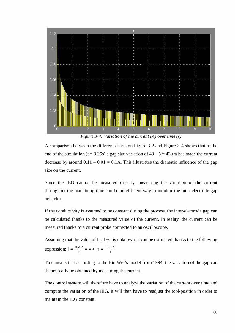
60
Figure 3-4: Variation of the current (A) over time (s)
A comparison between the different charts on Figure 3-2 and Figure 3-4 shows that at the
end of the simulation (t = 0.25s) a gap size variation of 48 – 5 = 43µm has made the current
decrease by around 0.11 – 0.01 = 0.1A. This illustrates the dramatic influence of the gap
size on the current.
Since the IEG cannot be measured directly, measuring the variation of the current
throughout the machining time can be an efficient way to monitor the inter-electrode gap
behavior.
If the conductivity is assumed to be constant during the process, the inter-electrode gap can
be calculated thanks to the measured value of the current. In reality, the current can be
measured thanks to a current probe connected to an oscilloscope.
Assuming that the value of the IEG is unknown, it can be estimated thanks to the following
expression: I = ==> h =
This means that according to the Bin Wei’s model from 1994, the variation of the gap can
theoretically be obtained by measuring the current.
The control system will therefore have to analyze the variation of the current over time and
compute the variation of the IEG. It will then have to readjust the tool-position in order to
maintain the IEG constant.

61
3.2. Bin Wei’s PECM gap model with constant feed rate
3.2.1. Mathematical formulation
Bin Wei modelled the process of pulse electrochemical machining (Rajurkar et al., 1993;
Wei, Rajurkar and Talpallikar, 1996) and his work is based on the model developed by
Kozak et al. in 1991 (Kozak, Rajurkar and Ross, 1991).
In this model, the evolution of the interelectrode gap (IEG) can be represented in Figure 3-5.
Figure 3-5: Interelectrode gap change during pulse cycle (Wei, 1994)
Assuming that (1) the electrolyte conductivity(κ ); (2) the current efficiency; and (3) the
over-voltage ΔU: E − E (where E and E are respectively the anode and cathode
overpotentials) are constant throughout the machining time, the Ohm’s law can be applied
in the IEG. From the conceptual equation:
Change in gap size = Anodic dissolution depth – Cathode feed distance
Wei developed a general IEG equation to model its behaviour during the machining process.
From equation (2-10):
Anodic dissolution depth = i . K . dt = κ . K . (U − ΔU )
h dt (3-6)

62
The cathode feed distance L can be calculated by:
L = V . dt (3-7) Where V is the feed rate of the tool-electrode in m/s.
Then the change in gap size dh during machining when the tool is moving towards the
workpiece at a constant feed rate can be expressed by:
dh = κ . K . (U − ΔU )
h. V − 1 × V . dt (3-8)
Wei observed that:
If h = h = κ . K (U − ΔU )
V then dhdt = 0. (κ = constant)
h is defined as the equilibrium gap size and is seen as a constant. Bin Wei (Wei, 1994)
highlighted that even if h was a solution of (3-8), reaching = 0 in PECM is impossible.
According to Wei the solution of equation (3-8) is given by the following expression:
h × lnh − hh − h + (h − h)− V . t = 0 (3-9)
Equation (3-9) describes the gap change considering the previous assumptions at any time
t during the pulse on-time t .
3.2.2. Simulation
To simulate the µPECM process with constant feed rate, the following model (Figure 3-6)
has been developed according to Wei’s model (1994). Since Ohm’s law can be applied
according to the assumptions of the model, the gap can be represented as a variable resistor
controlled by a signal that is function of the voltage (U) and the feed rate V .
The variation of h and the resistance of the gap (Rgap) have been computed over time
through the subsystem (1) with the equation: dh = . ( ) − V . dt
The resistance of the IEG is obtained using the formula: R = r × =

63
Figure 3-6: Matlab/Simulink model developed to simulate Wei's PECM model (1994) with constant feed rate
Figure 3-7: Internal diagram of the system (1) calculating the variation of h and Rgap with respect to U and Vf
With κ =10 S/m, the initial resistance of the gap is: R = ≈ 22 Ohms. A simulation
for 0.01 sec gives the following results with a constant feed rate of 1mm/min (Figure 3-8).
1
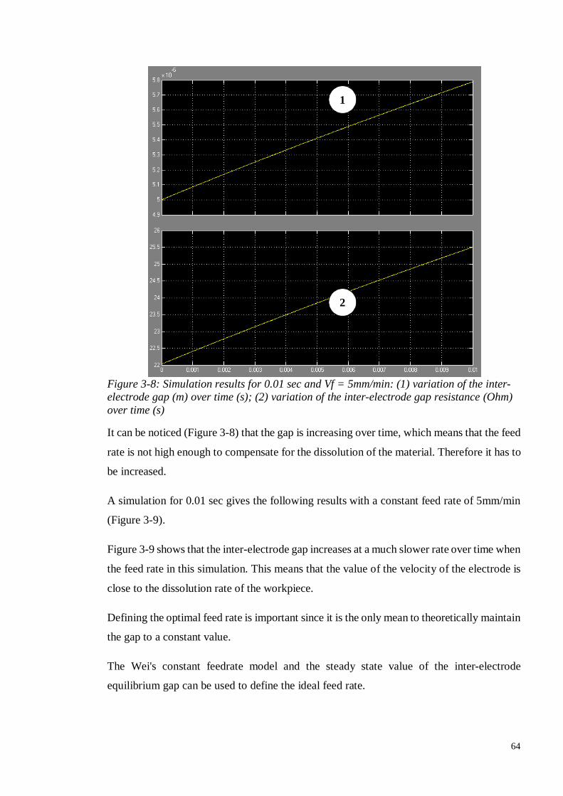
64
Figure 3-8: Simulation results for 0.01 sec and Vf = 5mm/min: (1) variation of the inter-electrode gap (m) over time (s); (2) variation of the inter-electrode gap resistance (Ohm) over time (s)
It can be noticed (Figure 3-8) that the gap is increasing over time, which means that the feed
rate is not high enough to compensate for the dissolution of the material. Therefore it has to
be increased.
A simulation for 0.01 sec gives the following results with a constant feed rate of 5mm/min
(Figure 3-9).
Figure 3-9 shows that the inter-electrode gap increases at a much slower rate over time when
the feed rate in this simulation. This means that the value of the velocity of the electrode is
close to the dissolution rate of the workpiece.
Defining the optimal feed rate is important since it is the only mean to theoretically maintain
the gap to a constant value.
The Wei's constant feedrate model and the steady state value of the inter-electrode
equilibrium gap can be used to define the ideal feed rate.
1
2

65
Figure 3-9: Simulation results for 0.01 sec and Vf = 5mm/min: (1) variation of the inter-electrode gap (m) over time (s); (2) variation of the inter-electrode gap resistance (Ohm) over time (s)
It has been seen previously that whatever the initial value of the gap is, the IEG will
converge towards a constant value over time. The optimal feed rate can therefore be found
with the following expression:
V =κ . K (U − ΔU )
h (3-10)
With the values from the previous model the optimal feed rate is:
κ = 10 S/m; K = 0.0281. 10 m /A. s; U − ΔU = 10V; h = 5.10 m
V =10 × 0.0281. 10 × 10
5.10 ≅ 5.62.10 m/s
However, since the pulse on-time represents 1/6 of the pulse period, this result has to be
divided by 6. Finally, V = 0.936667 × 10 m/s.
The calculation time of the previous model was very long, another similar model has
therefore been made without using P-SIM components (Figure 3-10). Thanks to this model
the calculation time is reduced and the model can therefore be simulated for a longer period.

66
Figure 3-10: Scheme diagram of the Matlab model used to define the optimal theoretical
feed rate
A simulation with the optimal feed rate value of the feed rate gives the results in Figure 3-11
and Figure 3-12.
Figure 3-11: Measured variation of i (A) over time over time before and after the Zero-
Order Hold block
It can be observed (Figure 3-12) that the inter-electrode gap slightly decreases over time
before reaching the steady state value of the equilibrium gap. It is linked to the fact that the
value of the constant feed rate has been rounded from 0,936667 .10 m/s to
0,937 .10 m/s approximating the equilibrium inter-electrode gap to:
h =10 × 0.0281. 10 × 10
0,937 .10 × 6 = 4.9982 µm

67
Figure 3-12: Variation of the inter-electrode gap (m) over time (s) with a constant feed
rate of 0.937 × 10 푚/푠
The current is therefore maintained to the same value, throughout the machining time,
guaranteeing a constant material removal rate.
3.2.3. Concluding remarks regarding Bin Wei’s model with constant feed rate
The notion of equilibrium gap has been explained and a way to maintain the gap to a
constant value was theoretically verified. The feed rate has been adjusted to obtain the
desired inter-electrode gap. The simulations done in this part confirmed that an equilibrium
gap could be reached and this model can be used to define the optimal feed rate value.
This is however very hard to reach an equilibrium state in real machining conditions: a
short-circuit can occur and change the MRR within the gap. This leads to unstable
behaviour. This model is particularly suited for PECM at high current densities and large
machining gaps, but in µECM the gap and current densities are respectively much smaller
and lower.
3.3. µECM model according to Marla et al. Marla et al. (Marla, Joshi and Mitra, 2008) suggested that the removed material could be
calculated according to the following equation:
m = A. Sz. F κ
∂E ∂x n T = k. S. J. n . T (3-11)
where:

68
T is the total time of machining including the on-time and off-time
k =.
is a constant of electrochemical machinability.
S is the cross sectional area of the tool-electrode
n is the duty cycle of the pulses defined as:
n = T
T + T
J is the current density defined as (Marla, Joshi and Mitra, 2008)
J = κ∂E ∂x =
I S .
with a potential gradient in the x direction equal to ∂E ∂x = V
Figure 3-13: Schematic of the µECM process (Marla, Joshi and Mitra, 2008)
According to equation (2-10) and taking the current efficiency into account, the volume of
material removed throughout the µECM process can be calculated as follows:
m ρ = V = n . K . I. T (3-12)
This model expression is in agreement with Bin Wei’s model. However, the electrical
double layer (EDL) effect is not taken into account in their model.

69
3.4. The electrical double layer: study of existing models and simulation
3.4.1. Models of the electrical double layer effect on the gap voltage
In ECM the electrical model of the inter-electrode gap is a variable resistance. However, in
µECM the effect of the electrical double layer (EDL) is significant enough not to be
neglected (Spieser, 2011).
If the EDL charging time is equal to the pulse on-time, the potential at the EDL is always
varying, since the double layer capacitance is charged during each pulse. The expression of
the anodic over-potential is therefore (Schuster and Kirchner, 2004; Kim et al., 2005a; b;
Zhang et al., 2007):
E (t) = E 1 − e ≈ Etτ (Taylor approx. ) (3-13)
Where E is the stationary value of the over-potential, t is the polarization time and τ = RC
corresponds to the EDL charging time.
According to the Tafel equation, the expression of the current density during the charge of
the EDL is the following (Schuster and Kirchner, 2004; Kim et al., 2005a; b; Zhang et al.,
2007):
i (t) = i e( )≈ i e
× × (3-14)
Where i is the exchange current density, β is the transfer coefficient (usually equal to 0.5),
n is the number of electrons (2 and 3 for respectively the ions Fe II and Fe III), F is the
Faraday constant, R is the gas constant and T is the temperature (in °K).
The volume V of dissolved material after 1 pulse is therefore equal to:
V = K . i (t) dt = K . i e× ×
dt
V = K . iR TβnF
τE . [ e
× ×− 1]
(3-15)
However, Kozak claimed (Kozak, Gulbinowicz and Gulbinowicz, 2008) that the current
density going through the double layer was actually the sum of 2 different current densities:

70
The charging current: it is the current density that flows through the double layer
when it is getting charged
The faradaic current: it is the current density that participates in the dissolution of
the material when the electrical double layer is fully charged
The equation describing the evolution of the current during the charge of a capacitor is:
i(t) = C.dU(t)
dt (3-16)
Where C is the capacitance of the capacitor (in F) and U(t) is the potential applied to the
capacitor (in V).
According to the Butler-equation the values of the Faraday current densities at the tool and
at the workpiece are given by (Kozak, Gulbinowicz and Gulbinowicz, 2008):
At the anode: ifa = ia0(e(1−β)nF
RgT Ea(t)− e
(−β)nFRgT Ea(t)
)
At the cathode: ifc = ic0(e(1−β)nF
RgT Ec(t)− e
(−β)nFRgT Ec(t)
) (3-17)
The total currents at the cathode i and at the anode i can be expressed as follows:
i (t) = i (t) + i (t) = C .dE (t)
dt + i (e( ) ( )
− e( ) ( )
)
i (t) = i (t) + i (t) = C .dE (t)
dt + i (e( ) ( )
− e( ) ( )
) (3-18)
It has been previously seen that a certain activating voltage had to be applied for the
dissolution to occur and that the resulting current density was non-linear. In their patent,
Schuster et al. described the evolution of the EDL current density with respect to the
polarization voltage thanks to the chart in Figure 3-14 (Schuster and Kirchner, 2004).

71
Figure 3-14: Evolution of the gap current with respect to the applied voltage, Urkt : activating potential (V) , Up : Pulse amplitude (V) (Schuster and Kirchner, 2004)
3.4.2. Similarities with Zener diodes
It can be noticed that this current/voltage non-linear relationship is very similar to the one
of a Zener diode. Indeed, in a Zener diode, the current evolves with respect to a polarization
voltage according to the characteristic graph (Figure 3-15):
Figure 3-15: Evolution of the current (mA) in a diode with respect to its polarization voltage (V) (Technologyuk.net, 2011)

72
In the following model, the electrical double layer will therefore be represented in Figure 3-16.
Figure 3-16: Proposed inter-electrode gap model (Spieser, 2011)
According to Kirchoff’s law, in the proposed model, the current passing through the Zener
diode will be added to the charging current of the capacitor. The faradaic current density is
therefore represented by the current of the diode.
The model has been simulated with the following values:
Diode resistance of the double layers (diode): R = R = R = 5. 10 Ohm;
Polarization voltage: 0,5V; Pulse width: 10ns; Pulse period: 60ns; Electrolyte
Resistance: R 30. 10 Ohm;
Capacitance of the EDLs: C = C = C = 10. 10 F
The time constant of the above circuit τ is equal to (Van Damme et al., 2011):
τ = R .C . = 1
1C R + 2
C R≈ 2.3 × 10 s
(3-19)
The following chart shows the value of the current passing through the anodic EDL during
its charge (Figure 3-17):

73
Figure 3-17: Variation of the current density passing through the EDL of the anode during its charge (퐼 ) in A/m² over time (s) (Spieser, 2011)
The loading/unloading time constant is very small hence the curve representing the current
is very sharp.
Figure 3-18: Variation of the faradaic current passing through the EDL of the anode (퐼 ) in A/m² over time (s) (Spieser, 2011)
The above pulses (Figure 3-18) represent the faradaic current density that will take part in
the dissolution process of the workpiece.

74
Figure 3-19: Variation of the total current density ( ic + if ) flowing through the system
(A/m²) over time (s) (Spieser, 2011)
On the above graph (Figure 3-19), the total current density flowing through the system is
represented. It can clearly be seen that the total current is the sum of the faradaic and
charging ones.
Figure 3-20: Variation of the applied voltage (Pulses) (V) over time (s) (Spieser, 2011)
Figure 3-21: Potential at the EDL of the anode (V) over time (s) (Spieser, 2011)

75
By taking into account the electrical double layer, more realistic pulses have been obtained.
This part can be considered as a first exploration of the inter-electrode gap evolution. Pulses
have been applied to the gap and the influence of the electrical double layer on the current
response has been modelled. It has been confirmed that the current passing through the
system is the sum of the faradaic current and the charging current of the EDL (Spieser,
2011).
3.4.3. More realistic model of the IEG This model combines the gap model taking into the EDL and adds the effect of the cabling
on the overall machining current. The following values are taken:
Influence of connection cables: these cables connect to pulse PSU to the machining cell. It
is assume that the cables are made of copper which has an electrical resistivity of ρ =
16.78 nΩ. m. The cable is considered to be of length l = 0.12m and to have a cross-
sectional area of S = 2 × 10 m .
The cable resistance can therefore be calculated as follows:
R = ρlS = 16.78 × 10
0.12 2 × 10 m ≅ 0.001Ω (3-20)
The cable inductance is modelled by a 75nH inductor.
The electrolyte resistance is considered to have a conductivty 휎 of 13S/m. Assuming a gap
of 5µm and that the current flows only through the front face of a cylindrical cathode having
a diameter of 170µm, the electrolyte resistance in the IEG can be expressed the following
way:
R = hσS =
5 × 10 13 × π × (85 × 10 ) ≅ 16.94Ω (3-21)
The pulse on-time is set to 150ns whereas the pulse period is set to 1µs.

76
Figure 3-22: Picture of the more realistic model of the IEG
Using these values, the following results can be obtained:
Figure 3-23: Voltage pulses measured across the gap in V and time in s
It can be observed that in µECM the total amount of current flowing through the system is
not very high compared to conventional ECM. This is mainly due to the small size of the
tool reducing the active area dramatically, and therefore increasing the resistance in the gap.
In µECM the dissolution will show a stochastic behavior due to the variation of material
properties and composition as well as the variation of the electrical parameters of the
continuum and if for any reason the dissolution rate changes during the process, the inter-
electrode gap will not be maintained since the feed rate does not vary over time in the
previous model.

77
To adjust the feed rate according to the variation of the dissolution rate, a control system
has to be developed.
Figure 3-24: Faradaic current pulses, amplitude in A and time in seconds
3.5. 2D Drilling simulation with simple electrical double layer (EDL) model
Mathematical models have been developed to provide with a better insight of the ECM and
PECM processes (McGeough, 1974; Datta and Landolt, 1981; Rajurkar et al., 1993, 1995;
Floridor et al., 2004). However, in µECM these models cannot be applied anymore: the
inter-electrode gap size is so small (less than 10µm) that factors that were neglected before
(electrical double layer (EDL) effect, local electrolyte conductivity and electrical field
distribution) are now significant enough to change the machining process (Davydov, Volgin
and Lyubimov, 2004; Cagnon et al., 2003; Schuster et al., 2000; Kirchner et al., 2001; Marla,
Joshi and Mitra, 2008; Kozak, Gulbinowicz and Gulbinowicz, 2008).
Most of the simulation models reviewed are very computationally intensive and do not allow
simulations for a very long period of time (Hotoiu et al., 2011; Deconinck, Van Damme and
Deconinck, 2012b; Van Damme et al., 2011).
In this section a simplified µECM process model is proposed by assuming that the EDL
effect behaves like a low-pass filter that attenuates the pulses when either the frequency or
the IEG increase. This model can be used to quickly setup a machining session and estimate
the material removal rates for specific values of the machining parameters.
A simulation program has been developed using LabVIEW in order to study the influence
of the different machining parameter and to predict the shape of the machined hole. This
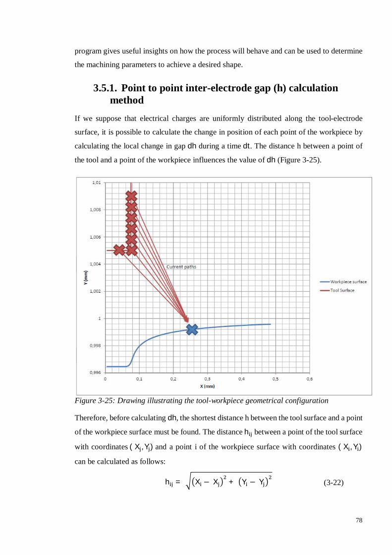
78
program gives useful insights on how the process will behave and can be used to determine
the machining parameters to achieve a desired shape.
3.5.1. Point to point inter-electrode gap (h) calculation method
If we suppose that electrical charges are uniformly distributed along the tool-electrode
surface, it is possible to calculate the change in position of each point of the workpiece by
calculating the local change in gap dh during a time dt. The distance h between a point of
the tool and a point of the workpiece influences the value of dh (Figure 3-25).
Figure 3-25: Drawing illustrating the tool-workpiece geometrical configuration
Therefore, before calculating dh, the shortest distance h between the tool surface and a point
of the workpiece surface must be found. The distance h between a point of the tool surface
with coordinates ( X , Y ) and a point i of the workpiece surface with coordinates ( X , Y )
can be calculated as follows:
h = X − X + Y − Y (3-22)

79
The number of points ( X , Y ) and ( X , Y ) depends on the resolution chosen. The algorithm
will calculate for each point ( X , Y ) all the possible gaps h and will then take the smallest
one.
3.5.2. Modelling the influence of the EDL on the gap change
The current density can be deduced thanks to Ohm’s law:
J = κ E (3-23) Where J is the current density (A/m², κ is the conductivity (S/m) of the electrolyte and E
is the intensity of the electric field in (V/m).
With c = κ . K (3-6) becomes:
dh =κ . K (U − ΔU )
h dt = c(U − ΔU )
h dt (3-24)
However, the above equation does not include the influence of the EDL on the process.
Schuster et al. mentioned that the electrical double layer can be modelled as a RC circuit,
which behaves like a low pass filter (Schuster and Kirchner, 2004; Schuster et al., 2000).
According to their work, the charging constant τ of EDL would be calculated as follows:
τ = hκ C (3-25)
It is important to mention that C is in µF/m². This equation respects the SI units because
farads are also seen as seconds/Ω.
Assuming that the capacitance of the electrical double layer C remains constant during
the process, it is possible to calculate the cut-off frequency f of the RC network:
f (h) = 1
2πτ(h) =1
2πR (h)C (3-26)
Where R is the resistance of the electrolyte through which the current is flowing to charge
the EDL and depends on the distance between the tool and the workpiece (IEG or h).
R is calculated as Wei and Marla suggested it, by considering that the conductive area of
the tool is equal to its cross section S:
R (h) = hκ S (3-27)

80
Following the properties of a low-pass filter, the amplitude of the pulses will decrease
depending on the frequency and the resistance R . This decreasing effect can be modelled
using the following formula to calculate the gain H(f).
H(h, f) =UU =
1
1 + ( 2πf2πf (h))
(3-28)
H(f) is used to calculate the amplitude of the voltage pulse which will remove material, and
the duty cycle n is added to the equation.
dh = c(n . U . H(h, f) − ΔU )
h dt (3-29)
Also, the impedance of the cabling has an influence on the process. The impedance of the
cable increases along with the pulse frequency f because of its parasitic inductance L. The
general formula to calculate the impedance Z is as follows:
Z(f) = R ² + (X (f))² (3-30)
Where the inductive reactance of the cable is: X (f) = 2πfL
To include the impedance of the cables, the equation to calculate dh is changed the
following way:
dh = K(n . U . H(h, f)− ΔU )
R (h) + Z (f) . Sdt (3-31)
Where Z (f) is the impedance of the cabling as well as the resistance of the tool electrode
(the ‘sys’ index is for system).
Also the current I can be calculated directly by applying the following formula:
I(h, f) =(n . U . H(h, f) − ΔU )
R (h) + Z (f) (3-32)
3.5.3. Simulation workflow
The workpiece Y position Y (t) can be calculated after each time step dt as followed:
Y (t) = Y (t − dt) − dh (3-33) Where Y (t) is the new Y position of the point of the workpiece is surface and Y (t − dt) is
the previously calculated Y surface position (at the simulation time t-dt).
The expression P(U , h ) can be described this way:

81
dh = K(n . U . H(h , f) − ΔU )
R h + Z (f) . Sdt (3-34)
At the beginning of the simulation, a squared mesh (Figure 3-27) is created according to the
geometrical configuration specified by the user.
Figure 3-26: VI creating the mesh for the simulation
Figure 3-27: Picture of the geometrical configuration created by the ‘Create Mesh’ VI
The removed depth at each time step is calculated according to the following algorithm
(Figure 3-28):
Every second during the simulation time, the position of the tool is updated and the new
workpiece surface is plotted.

82
For each point (퐗퐢,퐘퐢) of the workpiece surface do:
End of ‘for each point (푿풊,풀풊) of the workpiece surface do’
Figure 3-28: Simplified flowchart of the LabVIEW simulation programme
Figure 3-29 shows the final shape of the workpiece after a 50µm drilling session using
parameters in Table 3-1.
Frequency (Hz) 60000
Duty Cycle (%) 25
Off-time Offset (V) 0
Pulse amplitude (V) 8
Kv (cubic mm/As) 0.0281
Conductivity (S/mm) 0.013
EDL Capacitance (F/mm²) 1.00E-07
Activation Potential (V) 0.92
Current efficiency (%) 50
Feed Rate (mm/s) 0.000624
Simulation Time (s) 35
System Resistance (Ωs) 0.001
Table 3-1: Simulation parameters used to obtain the shape shown in figure 24.

83
Figure 3-29: Simulation results after a 50µm drilling simulation in 2D, the tool surface is
in red and the workpiece surface is in white.
The programme exports the machining results by creating a text file which can then be
imported in Microsoft Office Excel to in order to compare the different workpiece shapes
for different machining parameters.
3.6. Influence of the pulse frequency on the localization and the machining time.
In this simulation, the tool is fed towards the workpiece so that the IEG is maintained
constant. All the parameters (Table 3-2) except the frequency remain the same for the trials.
The machining is stopped as soon as a depth of 50µm is achieved.
From the results (Figure 3-30) it can be observed that the frequency has a dramatic influence
on the localization of the machining: at low frequency, the electrical double layer has less
effect and the current passing though the side walls of tool electrode removes material at
long distances from the desired machining region. This results in a hole with a relatively big
tapper angle and a greater diameter than the one of the tool electrode.
On the other hand, it can be noticed that when pulsing at high frequency the machining is
much more localized and the edge of the hole entry becomes sharper.

84
Frequency (Hz) from 60kHz to 1MHz
Duty Cycle (%) 25
Off-time Offset (V) 0
Pulse amplitude (V) 8
Kv (cubic mm/As) (100Cr6 alloy) 0.0281
Conductivity (S/mm) 0.0027 and 0.013
EDL Capacitance (F/mm²) 1E-07
Activation Potential (V) 0.92
Current efficiency (%) 50
Simulation Time (s) from 35s to 267s
Current efficiency 50%
Table 3-2: Machining parameters used for the simulations
Figure 3-30: Results of the simulation illustrating the influence of the pulse frequency at
different electrolyte conductivities Y and X positions are in mm.

85
However, at higher frequencies, the machining time to achieve the same depth is much
longer because the charging time of the EDL takes a greater portion of the pulse on-time at
higher frequencies and therefore the amount of faradaic current created during each pulse
becomes smaller.
Moreover, it can be seen that when the conductivity of the electrolyte is low, the effect of
the EDL is increased: the machining time becomes very long but the localization of the
dissolution process is better than with a conductivity of 0.013 S/m. A trade-off must
therefore be made in order to have an efficient and accurate machining process.
3.7. Summary In this chapter, the behaviour of the µECM process and the influence of the electrical double
layer have been modelled and simulated. The presented work is built over models found in
the literature review and provides an enhanced version of what has been achieved.
The models and concepts of Marla (Marla, Joshi and Mitra, 2008), Wei (Wei, 1994),
Schuster (Kozak, Gulbinowicz and Gulbinowicz, 2008) and Hocheng (Hocheng et al., 2003)
have been studied, verified and combined in this work.
A simplified model assuming that the EDL effect is similar to the effect of low-pass filter
was developed in order to simulate the µECM process for a long time.
The simulation programme provided realistic results and can be used to determine optimum
machining parameters. The influence of conductivity and frequency on the localisation and
the machining time were analysed. It was concluded that for a same frequency, the lower
conductivity electrolyte exploited at best the EDL effect, providing an improved
localization. However, a lower electrolyte conductivity and a higher pulse frequency will
increase the machining time. Therefore, a trade-off must be made between the precision of
the machining and the cycle time.

86
Chapter 4: AN INNOVATIVE PULSE POWER SUPPLY UNIT FOR µECM
It has been seen in the literature review that the power supply in µECM is a critical element.
Different circuits have been studied and 3 prototypes have been built in order to conceive a
pulse power supply meeting the requirements for µECM identified in the literature review:
Pulse frequency: 1kHz to 5MHz
Pulse width: 50ns to 1ms
Ultra-fast over current protection to protect the tool
Fully programmable with possibility to change parameters dynamically and during
machining
Possibility to reverse the pulse polarity to machine the tool without changing the
cabling
Possibility to create different pulse shapes to improve machining efficiency
This chapter presents an innovative pulse PSU for µECM. This prototype has been designed
following the power electronics fundamentals explained in Appendix 3 as well as the
development of two previous prototypes.
4.1. An novel pulse PSU architecture PSU a new design of pulse power supply is proposed to be able to perform an on line
machining of the cathode or to manufacture to or probes that are being clamped in the took
holder without having to manually swap the polarity by changing the cabling.
Proposed pulse power supply concept:
To be able to quickly reverse the pulse polarity, an H bridge circuit has been identified as
the most suitable circuit. It is composed of 4 N-type MOSFETs (SW1, SW2, SW3, and
SW4):

87
Figure 4-1: Schematic diagram of the first PSU prototype and its interfaces
When SW_pulse, SW1 and SW4 are turned on, a positive voltage is applied to the IEG and
the workpiece is machined.
When SW_pulse, SW2 and SW3 are turned on, a negative voltage is applied to the IEG: the
current will flow from the tool to the workpiece, which will machine the tool.
It is also possible to apply a positive voltage during the pulse on-time, followed by a
negative or positive voltage set by the PSU VOff-time during the pulse off time. This
configuration allows the creation of different pulse shapes to experiment the effect of the
polarization voltage during the pulse off-time. The pulse shapes that can be created with this
setup will be described in the section dedicated to the control circuitry.
4.2. Previous prototypes To facilitate the testing of the developed circuits and their prototyping, each PSU prototype
was separated in 3 parts:
The control part: controlling the power components
The power part: sending the voltage pulses to the gap
The over-current protection part: preventing short circuits from damaging the PSU

88
4.2.1. First prototype
The first prototype delivered the expected results despite off the noise present in the sensing
circuitry. However, some limitations have been observed:
The way the function generator was configured prevented a wide range of frequency
to be reached because a capacitance used with the oscillator could not be changed
dynamically.
There was no possibility to reverse to polarity in a programmed way. The only way
to do so was to swap the cable connections.
It was not possible to apply a negative or positive voltage offset voltage during the
pulse off-time.
The size of the board was too big and the footprint of the board needed optimization.
This prototype was mainly considered as a proof of concept to validate the choice for the
core components and the 3-board modular architecture. It has been deduced that this concept
would be a viable way to develop the other prototypes. The full research and development
for this prototype can be read in Appendix 4.
4.2.2. Second prototype
The second prototype used an innovative architecture which was first simulated using
MATLAB/Simulink (Appendix 5).
The second prototype can be seen as a proof of concept showing encouraging results
(Appendix 6). The pulse polarity as well as the offset voltage during off-time worked as
expected.
The new pulse generating module produced very accurate results and was a major
improvement with respect to the first prototype: the pulse frequency was varied from 2kHz
up to 5MHz. The drivers were drawing a lot of current at that frequency so the consumption
was high and the drivers were heating up. Heat-sinks have been added to help them cool
down.
This new prototype shall also offer more connectivity, with an isolated 24V digital
input/output interface to efficiently communicate with the motion controller of the machine.

89
However, the size of the board and the layout of the PSU could be respectively smaller and
more optimised. It was therefore decided to change the layout of the board, making a third
prototype.
Overall, this prototype provided a solid and innovative proof of concept for a pulse PSU
targeted for the µECM sector.
4.3. Pulse PSU prototype modules
4.3.1. The control circuitry
4.3.1.1. Pulse generating module
To control the switching of the MOSFETs a switching signal needs to be generated. The
frequency needs to be variable over a range, 1 kHz to 5MHz, with a duty cycle changing
from 5% to 100% (DC). Varying the frequency of the signal over such a large range is
uncommon, pulse width modulating the resulting signal, even more so. This means that this
part of the system becomes an important issue.
The solution adopted is shown in Figure 4-2 and uses two components: an oscillator and a
pulse generator.
Figure 4-2: Electrical schematic diagram of the oscillator and the pulse generator
Oscillator
The LTC6904 is a low power self-contained digital frequency source providing a precision
frequency from set through a serial port. This programmable oscillator is capable of
generating a 5V logic signal at a frequency varying from 1kHz to 68MHz. The LTC6904
requires no external components other than a power supply bypass capacitor, and it operates
over a single wide supply range of 2.7V to 5.5V.

90
The frequency of the oscillator is set according to the following equation (Linear
Technology, 2014):
f = 2 .2078(Hz)
(2− DAC1024)
(4-1)
OCT is a four-bit digital code and DAC is a ten-bit digital code. Evaluating this formula to
calculate OCT and DAC from a required frequency f, gives the following statements:
OCT = 3.22logf
1039 ,
DAC = round 2048−2078(Hz). 2( )
f (4-2)
The output of the programmable oscillator LTC6904 is connected to the trigger input of the
programmable pulse generator 3D7622-0.25 (Figure 4-2). The pulse generator will therefore
output pulses at each rising edge of the signal coming from the LTC6904, thus creating a
pulse train with adjustable frequency and duty cycle.
Modulation component
The Data Delay Devices 3D7622-0.25 device is a twenty two bit serial programmable pulse
generator that operates with either CMOS or TTL logic levels (Data Delay Devices, 2008).
A rising edge on the trigger input (TRIG) initiates a pulse, which is presented on the output
pins (OUT, OUTB) and ends at a time determined by the address loaded into the device via
SPI serial interface. The pulse width, programmed via the serial interface, can be varied
over 4,194,303 equal steps of 0.25ns. The 3D7622-0.25 has a minimum pulse width of
14.0ns and a maximum pulse width of 1.05ms. The pulse width can be varied according to
the formula (Data Delay Devices, 2008):
t = t + addr + t (4-3)
Where addr is the programmed address, t is the pulse width increment (equal to 0.25ns)
and t inherent pulse width (equal to 14ns). The device also offers a reset input (RES) to
terminate the pulse before the programmed pulse duration has expired.
The Arduino compatible Max32 development board is directly interfaced with the human
machine interface (HMI), which sends all the data necessary to configure the pulse PSU:

91
frequency, duty cycle, over current protection threshold and desired pulse shape. The
microcontroller then sets the frequency by communicating with the programmable oscillator
via I2C and also sets the duty cycle thanks to the pulse generator using the SPI
communication protocol.
4.3.1.2. Pulse shape selection
A multiplexer defines the polarity of the pulsed voltage. Signals PWM and PWM/
correspond respectively to outputs OUT and OUTB of the pulse generator. OUT and OUTB
generate signals that are logically inverted from each other: if OUT is HIGH (5V) then
OUTB is LOW (0V) and vice versa (Figure 4-3).
Figure 4-3: Control circuitry of the second PSU prototype
If PIN8 is LOW (0V), Channel A is selected, so SW1 and SW4 are synchronized with
SW_pulse whereas SW2 and SW3 are synchronized with SW_offtime. This results in the
configuration shown in Figure 4-4.
PIN8 (selects the logic of channel 1 & 2)
Signals coming from the pulse generator (pins OUT and OUTB)

92
Figure 4-4: Drawing representing the 4 different control signal used to change the pulse
shape when Channel A is selected.
If PIN8 is HIGH (5V), Channel B is selected, so SW2 and SW3 are synchronized with
SW_pulse whereas SW1 and SW4 are synchronized with SW_offtime. The following
signals are obtained (Figure 4-5):
Figure 4-5: Drawing representing the 4 different control signal used to change the pulse shape when Channel B is selected
The following drawing (Figure 4-6) describes the different pulse shapes that can be obtained
with the developed power supply:
Control signal for SW1 and SW4
Control signal for SW2 and SW3
Control signal for the Pulse switch
Control signal for the Offset switch
Control signal for SW1 and SW4
Control signal for SW2 and SW3
Control signal for the Pulse switch
Control signal for the Offset switch

93
Figure 4-6: Drawing of the different pulse shapes that can be obtained in the different configuration
4.3.1.3. 24V-logic isolated digital interface
The PSU is interfaced with the Power PMAC using optocouplers to guarantee the protection
of the microcontroller but also to shift the logic level from 3.3V (on the PSU side) to 24V
(on the Power PMAC side).

94
4.3.2. The power stage
4.3.2.1. Configuration
Different voltages can be applied to the H-bridge thanks to two MOSFETs, allowing to
apply a lower voltage during the pulse off-time. A Schottky barrier (D1) prevents current
from flowing from V_PULSE to V_OFFSET (because V_PULSE is greater than
V_OFFSET and the MOSFETs have built-in parallel diodes) (Figure 4-7).
Figure 4-7: Schematic of the MOSFETs switching between the PULSE and OFFSET voltages to be applied to the H-bridge
The drivers of the MOSFETs SW_pulse, SW_offset, SW1 and SW3 are isolated from the
ground thanks to 4 individual isolated DC-DC converters. This allows driving the
MOSFETs at a very wide range of frequencies and duty cycles.
To optimise the layout of the power stages, it has been decided that the drivers would be
powered by the control circuitry board. The isolated DC-DC converters are therefore not
present on the power stage, but on the control stage.
A pin connector placed close to the current sensing resistors allows the current sensing
circuitry board to be plugged onto the power stage. The output of the current sensing
circuitry board is interfaced with the control stage in order to interrupt the pulsing when the
over current protection is triggered.

95
Figure 4-8: Schematic of the MOSFETs and their drivers in the H-bridge
4.3.2.2. MOSFET selection The MOSFETs have been selected to the following criteria:
Operating voltage Operating current Turn-on and turn off-time Package shall allow soldering by hand
The selected MOSFET is a FDMS7578 from Fairchild Semiconductors (Figure 4-9). This
N-Channel MOSFET has been designed specifically to improve the overall efficiency and
to minimize switch node ringing of DC/DC converters using either synchronous or
conventional switching PWM controllers. It has been optimized for low gate charge, low
ON resistance (R ( )), fast switching speed and body diode reverse recovery performance
(Fairchild-Semiconductor, 2009).

96
Figure 4-9: CAD Model of the package (Power 56) and representation of the MOSFET FDMS7578 (Fairchild-Semiconductor, 2009)
The main characteristics of the FDMS7578 are summarised below (Table 4-1):
Parameters Value Unit Maximum drain to source voltage V 25 V
Maximum drain current I 17 continuous 60 pulsed A
Drain-source on resistance, R ( ) 0.0058 Ω Typical Turn-On Delay time 8 ns Typical Rise Time 2.6 ns Typical Turn-Off Delay time 20 ns Typical Fall Time 2.2 ns Maximum Gate-source voltage, V +/-20 V Gate-source threshold voltage V 1.6 V Source ohmic resistance 0.0025 Ω Drain ohmic resistance 0.0025 Ω Input capacitance C 1221 pF Reverse transfer capacitance C 54 pF
Table 4-1: Table summarizing the main characteristics of the MOSFET FDMS7578
4.3.2.3. Driver selection
The UCC27201DG4 high frequency N-Channel MOSFET driver includes a high-side/low-
side driver with independent inputs for maximum control flexibility. This allows for N-
Channel MOSFET control in half-bridge or full-bridge converters. The low-side and the
high-side gate drivers are independently controlled and matched to 1-ns between the turn-
on and turn-off of each other (TI, 2008).
In most cases, controlling the high-side MOSFET requires the use of a bootstrap diode and
a bootstrap capacitor to create a floating reference at its source - allowing a gate-source
voltage V to be applied. However the desired switching frequency of the pulse power
supply is too high to use such configuration. The high-side gate driver is therefore not used

97
and each MOSFET will have its own driver. A floating ground (GND_FLOAT) is provided
to the high-side drivers using an isolated 12V DC-DC converter (Figure 4-8).
4.3.2.4. Optimized layout for smaller footprint and reduced parasitics
The layout of the power board (Figure 4-10) has been designed to reduce the overall current
path across the PSU and a symmetrical configuration has been adopted to place the power
switches. The new placement of the MOSFET reduces the parasitic inductance of the board
and therefore reduces the amount of EMI generated (Jauregui, 2009).
Figure 4-10: PSU prototype layout to optimise the current path and reduce overall inductance. Arrows symbolise the direction of the current.
The cabling of the 3rd PSU is also different: flat braided cables have been used to reduce the
inductance of the cabling. The cables are directly soldered onto the board, to avoid the
parasitic inductance from cable connectors.
Some heat sinks have been placed on the MOSFETs and their drivers to help them cool
down when the pulse PSU is switching at high frequencies.

98
4.3.3. The over current protection (OCP) stage
The over current protection (Figure 4-11) on the second prototype is similar to the one on
the first prototype: the current is measured via a sensing resistor and sent to a comparator
as well as a peak detector. The comparator compares the measured current with a threshold
set by the microcontroller. On the other hand, the peak detector provides the control system
with a reliable current value.
Figure 4-11: Electrical diagram of the current sensing part on the OCP stage of the
second prototype:
Testing of the OCP stage
The OCP stage is mounted on the top of the power stage, as shown on the picture below.
The output of the PSU is connected to a 1Ω load.
On the Figure 4-12, the OCP can be seen triggering when the current goes above 3A. The
comparator output goes HIGH for a very short amount of time, but this time is sufficient to
make the SR flip-flop latch and stop the pulses.
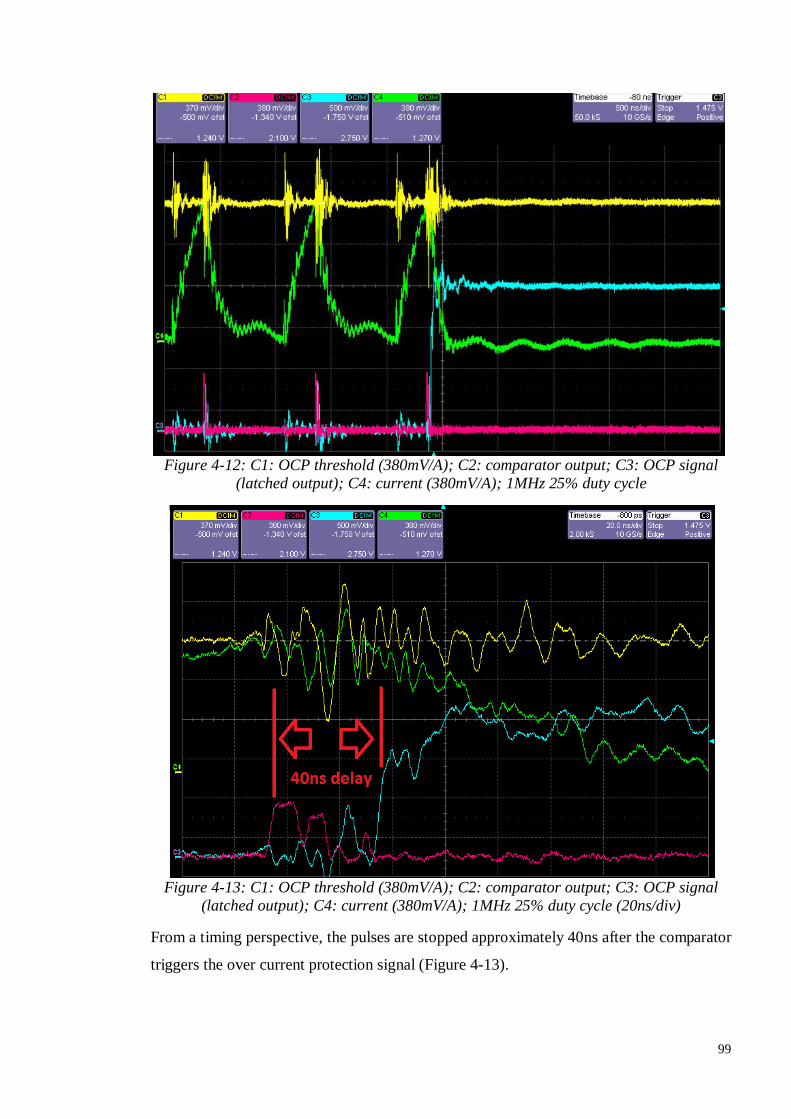
99
Figure 4-12: C1: OCP threshold (380mV/A); C2: comparator output; C3: OCP signal
(latched output); C4: current (380mV/A); 1MHz 25% duty cycle
Figure 4-13: C1: OCP threshold (380mV/A); C2: comparator output; C3: OCP signal
(latched output); C4: current (380mV/A); 1MHz 25% duty cycle (20ns/div)
From a timing perspective, the pulses are stopped approximately 40ns after the comparator
triggers the over current protection signal (Figure 4-13).

100
4.3.1. PSU testing and mounting
In this section, the output of the PSU is connected to a 1Ω 50W resistor which simulates the
gap and allows high current to flow through the PSU (as shown on Figure 4-14). Commands
are then sent to the PSU via the developed HMI and the obtained pulse shapes are visualized
with a scope. The current flowing though the resistor is measured thanks to a current
transformer.
The presented results have been obtained by connecting the output of the PSU to a 1Ohm
50W resistor used as a test load which allows high current (up to 7A for 7VDC) to flow
through the PSU (Figure 4-14). Commands are then sent to the PSU via the developed HMI
and the obtained pulse shapes are visualized with a Wavepro 7300A Lecroy oscilloscope.
The current flowing though the resistor is measured using a wide-band terminated current
transformer with a rise time of 7ns and a bandwidth of 60MHz model 13G1000 from Lilco
ltd.
Figure 4-14: Picture of the PSU being tested with the 1Ohm load and current transformer

101
Figure 4-15: C1: current (1V/A), C2: voltage; PSU in pulse mode 1: 3V pulse, no offset;
750kHz 25% duty cycle
Figure 4-16: C2: voltage; PSU in pulse mode 2: 2VDC (positive)

102
Figure 4-17: C1: current (1V/A), C2: voltage; PSU in pulse mode 3: 3V pulse, 1 V
negative offset; 750kHz 25% duty cycle
Figure 4-18: C1: current (1V/A), C2: voltage; PSU in pulse mode 4: 3V pulse, 1 V
positive offset; 750kHz 25% duty cycle

103
Figure 4-19: C1: current (1V/A), C2: voltage; PSU in pulse mode 5: 3V negative pulse, no
offset; 750kHz 25% duty cycle
Figure 4-20: C2: voltage; PSU in pulse mode 6: 2VDC (negative)

104
Figure 4-21: C1 current (1V/A), C2: voltage; PSU in pulse mode 7: negative 3V pulse, 1 V
positive offset; 750kHz 25% duty cycle
Figure 4-22: C1 current (1V/A), C2: voltage; PSU in pulse mode 8: negative 3V pulse, 1 V negative offset; 750kHz 25% duty cycle
Conclusion from tests with standard power cables
From the previous results, it can be seen that the parasitic inductance of the standard cables
is quite high as we can observe – particularly in mode 3 and 7 – a significant reverse voltage

105
peak after each pulse. This highlights the fact that low inductance cabling should be used to
improve the pulse shape.
The developed pulse PSU will enable to experiment the effects of the offset voltage during
the pulse off-time. Some papers advised a positive off-set during the pulse off time, which
would maintain the EDL constantly charged, whereas other papers mentioned that a
negative pulse off-time would enhance the machining process by accelerating the
unloading/reloading process of the EDL.
A lot of noise was generated when the power MOSFETs were being turned on/off. The
origin of this noise was mainly the high current transient across when the MOSFETs were
turned on /off. To reduce these current transient, a resistor has been added between the
output of the driver and the gate of the MOSFET. This resistor increases the turn on time of
the switch and therefore reduces the di dt⁄ across it. It is common practice to add a resistor
between the driver and the semiconductor switch. The literature review and the experiments
showed that at very high frequency the machining time dramatically increases (Mithu et al.,
2012). Therefore it was decided to add a gate resistor (4.7Ω) which should increase the turn-
on time but improve the quality of the output pulse as well as the current measuring board.
Since increasing the gate resistance also increases the turn off time, anti-parallel Schottky
diodes have been added to bypass the gate resistor during the turn off time, allowing for the
driver to sink the off time current in a faster way.
It was observed that when applying 6V pulses to the 1Ohm load at a frequency of 2.5MHz
and a duty cycle of 20%, the impedance of the cables becomes so important that only half
of the power is transmitted to the load. This highlights how essential a low inductance
cabling is for the µECM technology. The electrical specifications of the pulse PSU can be
found in Table 4-2.
Current Max 10A Frequency range 2kHz-8MHz Voltage max 15V Smallest pulse duration 50ns
Table 4-2: Specs of the developed pulse PSU
4.3.1.1. On-board signals
Different on-board signals can be observed while the PSU is pulsing (Figure 4-23). The
OCP level and measured current signals are constantly compared and as soon as the
measured current goes above the OCP level, the pulses are shut down. The peak value of

106
the current is sent to a motion controller which controls the IEG and proceeds to the tool
retraction when a short circuit is detected.
Figure 4-23: Oscilloscope screenshot of the measured signals on the PSU, 1MHz frequency, duty cycle of 25%, pulse amplitude of 3.2V and no offset during off-time 500ns/div.
Channel Description Scaling C1 Measured gap current via
commercial current sensor 1V/div., 1V/A
C2 Peak current value 250mV/div., 250mV/A C3 OCP threshold level 380mV/div., 380mV/A C4 Measured gap current via on-board
current sensing circuitry 380mV/div., 380mV/A
Table 4-3: Description of the signals measured in Figure 4-23.
4.3.1.2. OCP triggering trials
An important feature of the developed PSU is the time it takes for the pulses to be stopped
after the over current protection (OCP) has been triggered. This represents the time during
which the tool is exposed to an electrical and mechanical stress. The presented results are
obtained by short-circuiting the output of the pulse PSU and sending pulses (1MHz,
25%duty cycle, 2V pulse, 0V offset). The OCP signal triggered at the first pulse and the
pulses were stopped (Figure 4-24).
It can be seen from Figure 4-24 that the delay between the OCP being triggered and the
pulses being stopped is less than 50ns. The pulse duration is also reduced: instead of a 250ns
pulse, a short pulse of 150ns is generated.

107
Figure 4-24: Oscilloscope screenshot of the OCP signal delay 50ns/div. (C1: Measured gap current via commercial current sensor at 1V/div. and 1V/A; C2: OCP signal 1V/div; C3: OCP threshold level at 380mV/div. and 380mV/A; C4: Measured gap current via on-board current sensing circuitry at 380mV/A and 380mV/div.)
The results given in Figure 4-25: Graph representing the pulse amplitude at the IEG (mV)
according to the frequency (in kHz).show the variation of the pulse amplitude measured at
the gap according to the applied pulse frequency. For this, a 450µm copper tool-electrode
was used. The tool was moved towards the workpiece until electrical contact was made, the
OCP was set to 2A, the duty cycle was set to 15% and the pulse shape was set to 1.58V
during on-time and 0V during of time (referring to mode 1 in fig. 8). All the above
parameters were maintained constant during the experiment, the spindle was not spinning
and only the frequency was changed. The frequency was varied from 500kHz to 8MHz by
steps of 250kHz and the following values of the pulse amplitude at the IEG were measured.
Figure 4-25: Graph representing the pulse amplitude at the IEG (mV) according to the frequency (in kHz).

108
It can be observed from the graph that the voltage applied to the IEG becomes smaller when
the frequency increases. This phenomenon is due to the parasitic capacitance, resistance and
inductance of the cables which increase the impedance of the cable when greater frequencies
are applied.
It can be predicted from the graph (Figure 4-25) that significant material removal rate
(MRR) can be achieved at frequencies up to 2MHz, past this frequency, the amount of power
reaching the gap makes it hard to achieve an efficient machining process. This will have a
dramatic influence on the MRR but will improve the resolution of the machining because
of the higher frequencies (Mithu, Fantoni and Ciampi, 2011a).
The PSU has been installed on a self-developed µECM machine (Figure 4-26). A significant
effort has been taken to make the cables as short as possible:
The PSU is directly mounted on the Z axis very close to the tool-electrode;
When the electrode mounted on the Z axis is close to the workpiece, a second shorter
cable is connected to the machining cell in order to further reduce the length of the
current path during machining (Figure 4-26 (c)).
Figure 4-26: Pictures of the PSU mounted on the µECM machine.

109
4.3.2. Operation of the third PSU prototype
The firmware of the PSU has been programmed using the MPIDE developing environment.
This IDE allows you to write a programme, compile it and the download it to the Max32
development board via an USB cable. The programme will start executing as soon as the
Max32 is powered up, allowing it to run in standalone mode.
When the microcontroller receives the data from the HMI, it checks it the values for each
of the parameters are within a correct range. If that is the case, the microcontroller will
communicate with the following elements:
The square wave oscillator: The oscillator sets the frequency of the pulses and
outputs a square wave signal with the desired frequency. The communication
protocol between the microcontroller and the oscillator is I2C. The default I2C
communication library of the microcontroller is used to send the desired frequency
to the oscillator.
The pulse generator: The pulse generator outputs a pulse which has a programmed
duration each time its trigger input goes high. The output of the square wave
oscillator is directly wired to the trigger input of the pulse generator. The output of
the pulse generator is therefore a train of pulses set with a specified duration (duty
cycle) and frequency, which controls the on-times and off-times of the MOSFETs
on the power board. The pulse generator has a SPI interface which is also compatible
with the microcontroller and therefore the default SPI communication library can be
used.
Once the microcontroller has set the duty cycle and the frequency, it will set the pulse shape
and polarity using the AND logic gates and the multiplexer to select which channel with
control the power board.
Finally the microcontroller sets the OCP level by using one of its PWM outputs which is
sent to the low pass filter of which the output is connected to the negative input pin of an
ultrafast comparator.
The microcontroller then enables the output on the control board - which actuates the power
board - and starts polling on the serial communication for incoming messages (e.g. different
setting required) and for the OCP to trigger. If the OCP is triggered, the controller will
immediately reset the pulse generator and the disables the control channel. It is important to

110
mention that the OCP circuit has the power to disable the pulses on its own because the
protection logic is designed using solid state components (logic gates and SR latch) to
ensure the reliability and the deterministic timing of the protection.
Therefore, when the microcontroller detects that the OCP has triggered, pulses have been
disabled earlier and the system is protected already.
4.4. Discussion and conclusion for Chapter 3 The experience acquired when developing the previous prototypes allowed for the
optimization of the design in order to facilitate its integration in the machine. The small
footprint of the PSU makes its mounting on the Z axis easy. The new layout provided better
results at high frequency with less noise. The opto-isolated 24V logic interface made the
communication with the Power PMAC motion controller simpler and more reliable. The
reset of the OCP during machining was much faster because it was directly done using
hardwired circuitry and did not require the intervention of the HMI, resulting in improved
performance.
The design of a power supply capable of delivering ultra-short pulses and providing enough
power to the IEG is essential in order to progress in the development of µECM equipment.
In this Chapter, a device meeting the pulse PSU requirements for µECM has been designed,
developed and tested. An over current protection (OCP) system has been implemented to
protect the tool against undesired events occurring within the interelectrode gap during
machining.
A quick communication protocol between the power supply and the motion controller is
essential for the successful control of the µECM process. Therefore, the developed pulse
PSU provides the control system with signals such as the current peak value as well as the
OCP signal, in order to quickly react and adapt the motion of the tool.
In Sections 7.3, 7.4 and 7.5 of Chapter 7, the developed pulse PSU was used to produce
micro tools of different tip diameters (95µm, 57µm and 5µm) and drill a deep hole (1.1mm)
in 18NiCr6 with an on-line fabricated tool. The diameter (414µm) of the drilled hole was
relatively greater than the tool diameter. This result is mainly linked to 2 parameters: 1) the
tool run-out was quite significant 2) the machining time was very long so a bigger volume
was machined by the active sidewalls of the tool-electrode.

111
Chapter 5: MACHINE SYSTEM INTEGRATION This Chapter provides a detailed presentation of the µECM machine configuration. It has 3
axes of motion and a spindle allowing the tool-electrode to rotation during machining
(Figure 5-1). The rotation of the tool-electrode eases flushing of by-product and guarantees
that the holes drilled have a shape perfectly circular.
Description Value Slide Type Air bearing slides (5bar pressure) Accuracy (X, Y & Z axes) <1.0µm over total travel Stroke X: 200mm, Y: 200mm, Z: 150mm Resolution (X, Y & Z axes) 2nm Drive system (X, Y & Z axes) DC Brushless linear motor Controller architecture Open architecture motion controller Maximum current 5A Pulse frequency range DC or 1kHz – 5MHz Short circuit protection delay 50ns Tool retraction strategies Simple retraction mode
Custom retraction mode Process Control type Fuzzy logic & custom adaptive algorithms Machining operation µECM drilling (for hole drilling)
µECM turning (for micro-tool fabrication) Table 5-1: µECM machine specifications
The linear slides for each axis use air bearings with linear DC brushless motors and 2nm-
resolution encoders for ultra-precise motion. The control system is based on the Power
PMAC motion controller from Delta Tau. The electrolyte tank is located at the rear of the
machine and allows the electrolyte to be changed quickly.
A self-developed pulse generator has been mounted and interfaced with the machine and a
wire ECM grinding device has been added. The pulse generator has the possibility to reverse
the pulse polarity for on-line tool fabrication.
All the electrical components are located in a drawer under the machine, which makes the
machine look similar to the µMill (Luo et al., 2005; Nor, 2010). The machine (Figure 5-2)
consists of different subsystems which will be detailed below.

112
Figure 5-1: 3D-CAD models of the µECM machine.
Figure 5-2: Schematic diagram of the developed micro-ECM machine
5.1. Granite base In order to achieve ultraprecise motion to maintain the 5µm machining IEG, the material of
the base on which the slides are mounted must be very carefully selected.
Granite was chosen for the base in accordance to the requirements for ultra-precision
machines: it has a very low thermal expansion coefficient, good damping characteristics and

113
is very resistant to wear. Granite has always been a preferred material in the precision
engineering sector.
The axes are arranged in a gantry configuration where the X axis supports the Z axis and
the Y axis is directly mounted on the base (Figure 5-1). It was reported in the literature
review that this gantry configuration enabled a better overall machine stiffness in static and
dynamic conditions (Huo and Cheng, 2008; Cheng, 2008).
In order to isolate the machine from external vibrations, the base is mounted on four rubber
feet.
5.2. X, Y and Z Slides It has been identified in the literature review that the use of slides with aerostatic bearings
are the best way to reach precise and accurate motion in micro manufacturing applications.
Air bearings feature frictionless and backlash-free motion, high acceleration capabilities,
high accuracy and easy maintenance. The X, Y and Z slides implement a direct drive system,
which has proven to be the best choice in precision machining applications (Luo et al., 2005;
Nor, 2010; Wardle et al., 2010; Cheng, 2008).
Custom aerostatic slides were designed to achieve the best performance (Figure 5-3). Each
of the slides consists of a DC brushless linear motor with a trapezoidal hall sensor, a linear
encoder readhead with its scale and an air bearing.
Figure 5-3: Mechanical drawing of the assembled X slide and its cross-section

114
5.2.1. The linear DC brushless motor
The linear motors models are LEM-S-3-S from Anorad. Figure 5-4 illustrates the typical
assembly of the linear motor components. The coil assembly reflects the optional cooling
and Hall Effect sensor. A trapezoidal hall effect sensor is used to find the phase at motor
start up (Anorad Linear Motor Division, 1999). The motors therefore have two feedback
sensors for control: 1) the trapezoidal Hall Effect sensor and 2) the linear position encoder.
Parameters Model: LEM-S-3-S
Value
Continuous Force 75 N Peak Force 238 N Motor Constant 7.1 N/√W Thermal Resistance 0.89 °C/W Max Power Dissipation
113W
Maximum Applied Bus Voltage
325 Volts
Electrical Cycle Length
30mm
Electrical Time Constant
0.5msec
Force constant 16.7 N/A Back EMF constant p-p
V /m/s
Peak Current 14.3 A Continuous Current 4.5 A Phase to phase resistance
5.3 Ω
Phase to phase inductance
2.7 mH
Figure 5-4: Mechanical drawing and specifications of the LEM-S-3-S linear motor (Anorad Linear Motor Division, 1999)
Linear motors have several advantages over screw driven systems:
High Velocity
High Acceleration
Smoothness Of Motion
High Accuracy and Repeatability
High Stiffness
Low Maintenance and high Life Expectancy
Possibility for Clean Room And Vacuum Applications

115
Both of these feedback devices are interfaced with the motion control system via an
interface board Delta Tau ACC24E-2, which can control up to 4 axes simultaneously.
For the Z axis, the linear motor is mounted vertically and the weight of the slide is supported
by frictionless air cylinders. The weight of the Z slide is cancelled by adjusting the pressure
into the air cylinders so that the force of the motor is only used to move the slide. This
avoids motor overheating and prevents the tool from crashing into the workpiece in case of
power loss. Brakes are also mounted onto the air cylinders and are activated if there is no
air pressure, which prevents the Z slide from falling and being damaged.
5.2.2. Encoder system
The encoder system (Figure 5-5) is made of a readhead, an interpolator and a scale. The
models of these components are summarised in Table 5-2. Readhead Renishaw TONIC READHEAD 5m RELM/RSLM, Model T1011-50A.
Tonic, Linear, Standard Readhead, for RSLM/RELM Scales, all reference marks are output, cable length 5m. With standard mini connector to mate with Ti/TD interface.
Interpolator Renishaw TI 10KD A 20 A Digital, Tonic (Ti), Interpolation factor/resolution: 2nm (10KD), Line driven E output; All alarms (A), Minimum receiver clock frequency (40 MHz), Options: A = P/Q limits – ‘active high’, standard reference mark.
Scale Renishaw Scale - RSLM-SS-20U3A-0430-A Standard, high accuracy stainless steel scale, with a pitch of 20µm, a cross section of 15mm X 1.5mm and a spar length of 430mm.
Table 5-2: Summary of the components used in the encoder system
Figure 5-5: Mechanical drawing of the Renishaw encoder system
The encoder receiver frequency of the motion control system is set to 40MHz, which allows
a maximum speed of 0.054m/s on each axis. This speed is more than sufficient because the
tool feed rates during the machining process is very low. The 2nm encoder resolution of the
position feedback system allows a very precise motion of the slides. A reference mark is

116
located in the middle of the scale and is used at initialization to setup the axis (during phase
and home search).
5.2.3. The air bearings
Figure 5-6: Picture of the groove pattern machined in the inner surface of the pressurized bearing to improve stability. The encoder read head can also be seen.
The air bearings play a crucial role in ultra-precision motion. One of the major features of
the machine tool is that aerostatic bearings are used for all axes, which differs from the
situation for all of the µECM machines in the market. The air bearings consist of a sliding
cage which is made of brass assembled around a granite beam. The linear slides are based
on new novel aerostatic bearing technology which improves the stiffness and load capability
by 50% (Huo, Cheng and Wardle, 2010a). A very specific groove pattern (Figure 5-6) has
been machined on the air bearing surface to improve stability as mentioned by Luo et al.
(2005) and Stanev et al. (2004) (Luo et al., 2005; Stanev, Wardle and Corbett, 2004).
Therefore, sub-micron motion accuracy is ensured by the above technologies. The clearance
between the brass plates and the beam surface has been optimized for better performance of
the slides.
5.3. The spindle The spindle of the µECM machine is made of a stepper motor and a rotating part holding
the tool-electrode.
The spindle (Figure 5-7) rotates the electrode during machining in order to reduce the
influence of the asymmetric imperfections of the tool-electrode (run out). This spindle uses

117
a stepper motor, which allows precise positioning when tool-electrodes with different
shapes are needed (triangle, square etc.).
In µECM, tool-electrodes with simple shapes (cylindrical or semi-cylindrical (Yang, Park
and Chu, 2009)) are used in most cases. The electrical connection of the cathode is complex
to achieve because the tool is spinning: energy must be reliably transmitted to the rotating
element. In the case of high frequency power supply and high current it is not suitable to
use the traditional carbon or silver brushes because the transmission of high current has a
detrimental effect on them and they do not work well at high frequency (parasitic
inductance).
At the moment there is no good solution on the market such as a system transmitting high
frequency signals and high current to a spinning electrode and at the same time to be located
as close as possible to the IEG (with a minimal length of metal conducting the pulses).
Figure 5-7: Cross section of the developed spindle for the µECM machine. For safety reasons, the mercury slip ring was later replaced by a ring with microfiber carbon brushes.
The solution adopted by the author was to develop a purpose built spindle (Figure 5-7) using
precision bearings and to have the transmission of the signals to be done via a ring with

118
microfiber carbon brushes. This type of ring is normally used for shaft grounding and
bearing protection, and is able to handle high current at high frequencies (Muetze and Oh,
2008).
To improve the electrical contact between the brushes and the tool-electrode, a silver coating
was applied on the surface of the electrode-holder. This setup makes a reliable connection
between the PSU and the rotating parts of the spindle which holds the tool-electrode.
The stepper motor on the spindle is the model ST4218L1806-LC-NEU from Nanotec which
can be controlled using a SMCI33-1 drive. The step angle of the motor is 1.8 degrees with
an accuracy of +/- 5%. The drive communicates with the HMI using a USB port (Figure
5-8).
Figure 5-8: Schematic diagram showing the wiring of the stepper motor as well as its interface with the HMI.

119
5.4. Electrical cabinet The electrical cabinet (Figure 5-9) is located in a ‘drawer’ under the base of the machine. It
contains all the electrical components necessary to operate the machine. Each of these
components will be detailed in the following sections.
Figure 5-9: Picture of the electrical cabinet
5.4.1. Control components
5.4.1.1. Power PMAC motion controller
The control system is the one of the most innovative part of the machine. As special process
control algorithms need to be developed, a controller with an open architecture should be
chosen is order to facilitate the development. The Delta Tau Power PMAC suits perfectly
to the requirement: it can run PLCs and programs which are either written in C or in PMAC
script language (which is a proprietary programming language from Delta Tau).
The Power PMAC is actually a computer on a single board which can be interfaced to an
extensive range of compatible Delta Tau motion control, analogue input/output and digital
input/output boards. The Power PMAC runs a Linux Debian distribution whose kernel has
been patched with the open-source real time extension Xenomai to give real time
capabilities to the operating system (Barbalace et al., 2008).
It is very important for a control system to be real-time in order to ensure a deterministic
behaviour in cases where hazardous events could occur.
The Delta Tau Power PMAC CPU board is placed into a UMAC rack (Figure 5-10) and
interfaced with the following boards.

120
Figure 5-10: A picture representing the UMAC rack as a modular system.
Source: http://www.heason.com/catalogue/74/umac.html
5.4.1.2. ACC24E-2 4 axes interface board
This motion control board allows the Power PMAC to control up to 4 axes. The inputs of
this board are the encoders and the hall sensors of the X, Y and Z axes (Figure 5-11 and
Figure 5-12).
The connections between the encoders and the Acc24E-2 are made via a Ziplink DB15 to
Terminal Block adapters using the following connection list:
TB1 Pin1 => Pin 14 (A+) TB1 Pin 2 => Pin 6 ( A-) TB1 Pin 3 => Pin 13 (B+) TB1 Pin 4 => Pin 5 (B-) TB1 Pin 5 => Pin 12 (Reference mark Z+ = C+ ) TB1 Pin 6 => Pin 4 (Reference mark Z- = C- ) TB1 Pin 7 => Pin 7,8 (+5V) TB1 Pin 8 => Pin 2,9 (0V, GND)
The Hall sensors are connected the following way:
RED = HALL +5V => TB7 BLACK = GND => TB8 WHITE= S1 = Phase U => TB9 BLUE = S2 = Phase V => TB10 ORANGE = S3 = Phase W => TB11
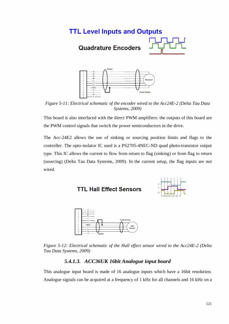
121
Figure 5-11: Electrical schematic of the encoder wired to the Acc24E-2 (Delta Tau Data
Systems, 2009)
This board is also interfaced with the direct PWM amplifiers: the outputs of this board are
the PWM control signals that switch the power semiconductors in the drive.
The Acc-24E2 allows the use of sinking or sourcing position limits and flags to the
controller. The opto-isolator IC used is a PS2705-4NEC-ND quad photo-transistor output
type. This IC allows the current to flow from return to flag (sinking) or from flag to return
(sourcing) (Delta Tau Data Systems, 2009). In the current setup, the flag inputs are not
wired.
Figure 5-12: Electrical schematic of the Hall effect sensor wired to the Acc24E-2 (Delta Tau Data Systems, 2009)
5.4.1.3. ACC36UK 16bit Analogue input board
This analogue input board is made of 16 analogue inputs which have a 16bit resolution.
Analogue signals can be acquired at a frequency of 1 kHz for all channels and 16 kHz on a

122
single channel. This board is used to acquire the peak value of the measured machining
current.
The ACC36UK is a special card and is therefore not detected automatically by the Power
PMAC. Even though it does not have automatic detection hardware, their outputs can still
be cleared at start-up using a custom programme written in C. The base addresses the I/O
cards occupy must be known. The base addresses correspond to which jumper settings (or
SW1 if a newer card) are used on the I/O card; for example, E1-E4, shown on page 15 of
the ACC-11E manual, set the base address for ACC-11E (Delta Tau Data Systems, 2011).
The address of the board is set using the DIP switch configuration shown in Table 5-3.
Chip select Base address (Turbo PMAC) 8 7 6 5 4 3 2 1
CS14 Y:$78E00 ON OFF OFF OFF ON OFF OFF OFF
Table 5-3: Table of the DIP switch configuration used to set the address of the Acc36UK
$78E00 $C00000 for Power PMAC, index of the board will be 1.
Each card's manual will describe how to set the jumpers or SW1 setting for various base
addresses. A document correlating Turbo PMAC base addresses to the Power I/O base
address offsets needed for Power PMAC was used to access to the data acquired in each
channel of the ACC36UK.
To point to the card, piom (pointer to I/O memory) must be added to the value given in the
Power PMAC I/O Base Address Offset, divided by 4, and point thereto using a volatile
unsigned int pointer.
To access an undetected card the definitions of the pointers toward the ACC36UK memory
must be made. For the base address of $78E00 ($C00000 on Power PMAC), the following
pointer configuration is obtained (Figure 5-13).
The defined pointers are then used in the C function GetAcc36UKValue() in the programme
bgcplc0.c (Figure 5-14).

123
Figure 5-13: ACC36UK memory pointers setup in the global definitions.pmh file of the Power PMAC IDE
Figure 5-14: The function GetAcc36UKValue() using pointers to access the data acquired by the ACC36UK in C.
5.4.1.4. ACC65E digital input/output board
This digital input/output board is used to receive logic signals from the pulse power supply
and all the safety related components. Its outputs are used to switch on relays and
enable/disable features on the pulse power supply.

124
The controller is the UMAC rack containing the Delta Tau Power PMAC and its control
boards, which will be described later on.
5.4.1. GeoDrive direct PWM amplifiers
The GeoDrive direct PWM amplifiers are controlled by the PWM logic signals coming from
the ACC24E-2. The model used is the GPL052 and its characteristics are summarized in
Table 5-4. Each amplifier has two control inputs (with 36-pin mini-D connectors) and is
able to power two motors. Therefore two amplifiers are needed to control the 3 motors for
the X, Y and Z axis. The first drive ‘PWM1’ powers axes X and Y whereas the second one
‘PWM2’ is used for the Z axis.
Main input power: Nominal Input voltage: 230VAC Rated input voltage: 97-265VAC Rated Continuous input current:
6.6 AAC(rms) Rated input Power: 2629W Frequency: 50Hz Phase requirements: 3 Main bus capacitance: 3380µF
Output power: Rated output voltage: 138V Rated continuous output current
per axis: 5A Peak output current for (2 seconds):
10A Rated output power per axis: 1195W
Bus protection : Nominal DC bus 325 Over-voltage trip level (VDC): 410 Under-voltage Lockout level (VDC):
10
Shunt regulator ratings: Turn-On Voltage (VDC) : 392 Turn-Off Voltage (VDC) : 372 Delta Tau Recommended Load
Resistor (300 W Max.) : GAR78
Control logic power:
Input Voltage (VDC): 20-27 Input Current (A): 2A Inrush Current (A): 4A
Current feedback:
Resolution (bits) : 12 Full-scale Signed Reading (±A) :
16.26
Transistor Control:
Delta tau recommended PWM frequency (kHz) : 12
Minimum Dead Time (µs): 1 Charge Pump Time (% of PWM
period): 5
Table 5-4: Summary of the specifications of the direct PWM drive GPL052 (Delta Tau Data Systems, 2006)
The amplifiers also need a 24VDC source to supply their logic unit which controls the power
semiconductors chopping the rectified 138VDC voltage. The installation manual claims that
‘This [24VDC] power can remain on, regardless of the main AC input power, allowing the
signal electronics to be active while the main motor power control is inactive.’ (Delta Tau
Data Systems, 2006).

125
The rated input voltage is 230VAC and therefore each amplifier is power by 1 phase. The
3rd phase ‘L3’ is connected to ‘PWM1’ and the 2nd phase ‘L2’ powers ‘PWM2’ (Figure
5-15).
Figure 5-15: Electrical schematic of the wiring of the amplifiers
5.4.2. 24V logic and electrical Safety components
5.4.2.1. 24V logic components
The ACC65E uses logic signals with voltages in the 12-24V range and therefore an external
24V DC power supply is needed. A 24VDC signal is produced by an Omron S8VS-18024
power supply.
Two Siemens 3-phase contacts relays (3RT10161BB42) are placed between the AC voltage
supply and the inputs of the GeoDrive amplifiers (Figure 5-15). The first is controlled by
the Power PMAC and is used to enable/disable the amplifiers for safety purposes.
A 3RT19161DG00 suppression diode is added to the relays to avoid any damage when
releasing the current of coil at turn-off.
An emergency stop button is connected to one of the contact relays in order to cut-off the
power to the drives quickly and reliably in case of dangerous situation.

126
A relay is also used to turn on/off the pump. The 24V logic of the relay is connected to the
digital output ‘DO2’ of the board ACC65E.
5.4.2.2. Circuit breakers
To protect the controller, a 6A circuit breaker with a B curve has been selected (B6).
For the 24VDC PSU, a C6 circuit breaker was chosen. The direct PWM amplifiers are
protected by B16 circuit breakers.
For the PC running the HMI, a B6 circuit breaker was initially chosen, but it seemed like
the in rush current of its power supply was too high and made the circuit breaker trigger at
power up. Therefore, it was replaced by a C6 circuit breaker.
5.4.3. Filtering and shielding
The 3-phase + neutral line filter FN256-16-46 from Schaffner is a general purpose filter
which acts as an EMI filter and improves the power quality.
It helps reducing noise and prevents the machine from being affected by other events on the
network (voltage spikes, etc...).
The cables connecting the drives to the linear DC motors are shielded to reduce the emission
of noise linked to the switching power conductors.
5.5. Electrochemical machining cell and electrical connections
The electrochemical machining cell has been designed to machine workpieces which have
the shape of a coin. These parts were provided by the company Delphi (UK) and used in the
fuel injection system of diesel engines. The electrochemical cell has 3 holes: 1 electrolyte
inlet delivering the fresh electrolyte to the working zone and 2 electrolyte outlets taking the
already used electrolyte to the filtering station.
The part to be machined is clamped using a cap that is bolted on the top of the cell. This cap
not only maintains the workpiece in position, but it is also made of conductive material to
connect the workpiece to the pulse PSU.
In electrochemical machining the electrical connections must not be exposed to the effect
of the working electrolyte. The part to be machined is clamped using a cap that is bolted on
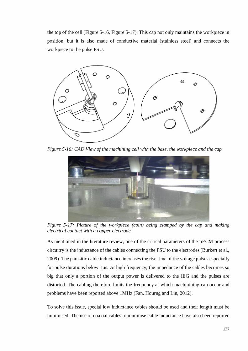
127
the top of the cell (Figure 5-16, Figure 5-17). This cap not only maintains the workpiece in
position, but it is also made of conductive material (stainless steel) and connects the
workpiece to the pulse PSU.
Figure 5-16: CAD View of the machining cell with the base, the workpiece and the cap
Figure 5-17: Picture of the workpiece (coin) being clamped by the cap and making electrical contact with a copper electrode.
As mentioned in the literature review, one of the critical parameters of the µECM process
circuitry is the inductance of the cables connecting the PSU to the electrodes (Burkert et al.,
2009). The parasitic cable inductance increases the rise time of the voltage pulses especially
for pulse durations below 1µs. At high frequency, the impedance of the cables becomes so
big that only a portion of the output power is delivered to the IEG and the pulses are
distorted. The cabling therefore limits the frequency at which machinining can occur and
problems have been reported above 1MHz (Fan, Hourng and Lin, 2012).
To solve this issue, special low inductance cables should be used and their length must be
minimised. The use of coaxial cables to minimise cable inductance have also been reported

128
(Park, Kim and Chu, 2006). This would mean that the PSU has to ‘be positioned as close as
possible at the gap connection’ (Burkert et al., 2009).
The solution adopted by the author to minimize the cable length was to mount the pulse
PSU directly on the Z axis, very close to the spindle.
The machining cell also allows the installation of a wire to perform the machining of micro-
tools and micro-probes. Metallic washers assure the wire fixture and electrical connection
(Figure 5-18).
Figure 5-18: Picture of the electrochemical cell with a wire installed for micro-probe machining

129
5.6. Electrolyte circuit
Figure 5-19: Picture of the 2 filters and the pump
Pump: The pump is a single phase Iwaki Magnet Pump model MD-20RZM-220N.
It has 2 poles and has power consumption of 45-57W. It works directly from the
mains electrical supply (220V/50Hz) and is protected by a 1A circuit breaker. The
chamber of the pump is made of chemical resistant material, allowing the use of
corrosive electrolyte such as aqueous solutions of sulphuric acid or hydrochloric
acid.
Filters: Two inline filters made of spun polypropylene (of the type used for micro-
EDM machining) with a fineness of 5μm and 1μm were chosen to accomplish the
electrolyte filtration task (Figure 5-19). The filter cartridges are of 2.5 inch dia. and
10 inch length and fit into a housing bowl. The inlet and outlet ports of the housing
bowls have a 3/4inch diameter.
Valves: A system of valves allows the user to select the electrolyte path. The user
can either supply the workpiece clamped in the electrochemical cell or supply the
wire-µECM process through a nozzle (Figure 5-18).
Flexible pipes: The flexible pipes (Cole-Palmer C-Flex clear, EW-06422-16 – 7
metres length approx.) will carry the electrolyte supply system to the machining cell.
Their flexibility allows the positioning and motion of the cell at different locations.
Electrolyte container: The electrolyte is stored in a tank located in a thermally
controlled container. The chosen container is the Waeco Tropicool TC-35FL-AC
Container.

130
Temperature control is an important factor within the machining process. As the temperature
increases, the conductivity increases which can influence the MRR. Therefore the
electrolyte container helps maintaining the temperature of the electrolyte constant. Holes
had to be drilled where the electrolyte is piped to and from the container.
5.7. Conclusions In this chapter, the machine integration and the interfaces between its different subsystems
were presented. State of the art components were selected in order to meet the required
specifications identified after an in-depth research and analysis.
The presented machine provides outstanding capabilities in terms of programmability and
precision motion thanks to the Delta Tau Power PMAC control system interfaced with 2nm
resolution encoders.
The unique cell configuration allows the fabrication of micro-tools and the machining of
parts on a single setup and in a sequential manner.
This research and development can lead to various applications such as the drilling of micro-
holes in hard to machine material for the automotive and aerospace sectors. Each of these
applications will require the design of an adapted workpiece clamping system which should
meet the electrical and spatial requirements for an optimal machining performance (short
current path for high frequency, chemical resistant fixtures…).

131
Chapter 6: PROCESS CONTROL AND SUPERVISION 6.1. Servo loop tuning of the X, Y and Z axes
The servo algorithm controlling the position and the velocity of the X, Y and Z axes is a
PID with velocity and acceleration feed forward loops.
The proportional (Kp), integral (Ki), derivative (Kd), velocity feed forward (Kvff) and
acceleration feed forward (Kaff) have to be accurately tuned for each axis in order to achieve
an optimum performance.
The tuning of the control loop is done using the interactive tuning feature of the Power
PMAC Suite software.
At the beginning, the step response test is made: A voltage step is applied to the motor and
the velocity and position are plotted over time. Kp is progressively increased until the rise
time is short enough and an overshoot is reached. The derivative gain Kd can then be
adjusted to reduce the overshoot and damp the system response (Figure 6-1).
The role of Ki is to eliminate the steady state error, it must be high enough to reduce it
rapidly but increasing it also increases the overshoot of the step response.

132
Figure 6-1: Flow chart of the PID tuning method (Nor, 2010).
Once the PID gains have been set properly and the desired step response is obtained (Figure
6-2), a parabolic velocity curve response can be plotted in order to setup the velocity and
the acceleration feed forward curves (Figure 6-3).

133
Figure 6-2: Plot of a step response step used to setup the PID gains of motor 2.
The position following error can be used as a criterion to determine the precision at which
the motion is being performed. In Figure 6-3 it can be seen that the maximum following
error is approximately 34 motor units. Motor units correspond to encoder counts so 1 count
represents 2nm. The following error of the Y axis is therefore 68nm on a parabolic move,
which is an acceptable amount of error and better than most of the ultra-precision motion
linear stages available on the market which usually have a 0.1µm accuracy.
Figure 6-3: Plot of a parabolic move used to setup the feed forward gains of motor 2.
The following configurations are currently used for each motor and guarantee a very precise
motion with following errors below 0.1µm for all axes. The values of the parameters are
specific to the cycle time of the servo loop of the controller. If the servo cycle time is
changed, these coefficients are not suitable anymore and the motors have to be tuned again:

134
Motor 1 (X):
Motor[1].Servo.Kp = 0.80000007; Motor[1].Servo.Kvfb = 12; Motor[1].Servo.Ki = 0.0070000001; Motor[1].Servo.Kvff = 12; Motor[1].Servo.Kaff = 15;
Motor 2 (Y) (implemented with a Notch filter to improve stability):
Motor[2].Servo.Kc1=-1.67232439712759 Motor[2].Servo.Kc2=0.90811731417569 Motor[2].Servo.Kc3=0 Motor[2].Servo.Kc4=0 Motor[2].Servo.Kc5=0 Motor[2].Servo.Kc6=0 Motor[2].Servo.Kc7=0 Motor[2].Servo.Kd1=-0.904859562345772 Motor[2].Servo.Kd2=0.277998561498207 Motor[2].Servo.Kd3=0 Motor[2].Servo.Kd4=0 Motor[2].Servo.Kd5=0 Motor[2].Servo.Kd6=0 Motor[2].Servo.Kd7=0 Motor[2].Servo.SwPoly7=0 Motor[2].Servo.Kp=0.332322052212607 Motor[2].Servo.Kvfb = 5; Motor[2].Servo.Ki = 0.005; Motor[2].Servo.Kvff = 5; Motor[2].Servo.Kaff = 0;
Motor 3 (Z):
Motor[3].Servo.Kp = 0.8; Motor[3].Servo.Kvfb = 12; Motor[3].Servo.Ki = 0.006; Motor[3].Servo.Kvff = 12; Motor[3].Servo.Kaff = 12;
6.2. Orbiting motion A function allowing the orbiting of the tool electrode has been developed to allow the
machining of features bigger than the tool diameter using the ‘electrochemical micro
milling’ technique.
The X and Y positions of the stages have been recorded for 10seconds when the orbiting
motion program was started. The following chart (Figure 6-4) displays the trajectory of the
tool. It can be seen that even at a small scale, the reproducibility of the motion is very
acceptable, with very small position differences.
The program needs to be given an orbiting radius, the centre of the orbiting movement and
the feed rate.

135
Figure 6-4: Plot of the tool trajectory in the X, Y plane when the orbiting motion program is executed, the position is in motor units, corresponding to 2nm/unit. The radius of the orbiting movement was therefore 100µm.
This program only affects the X and Y axis, which means the Z axis can be controlled
independently in another program like the fuzzy control state machine. In case of OCP, the
orbiting motion program should be able to stop the motion immediately to avoid the tool
electrode from being damaged.
6.3. Machine initialization algorithms At power up, the absolute position of each of the axes is unknown. Therefore, before
beginning any operation, all the axes much find their home position. For this purpose,
special programs have been written for each motor:
Plc 2: Does the setup of the X axis
Plc 3: Does the setup of the Y axis
Plc 4: Does the setup of the Z axis
These programs follow the same structure and their logic has been summarized in the flow
chart in Figure 6-5.
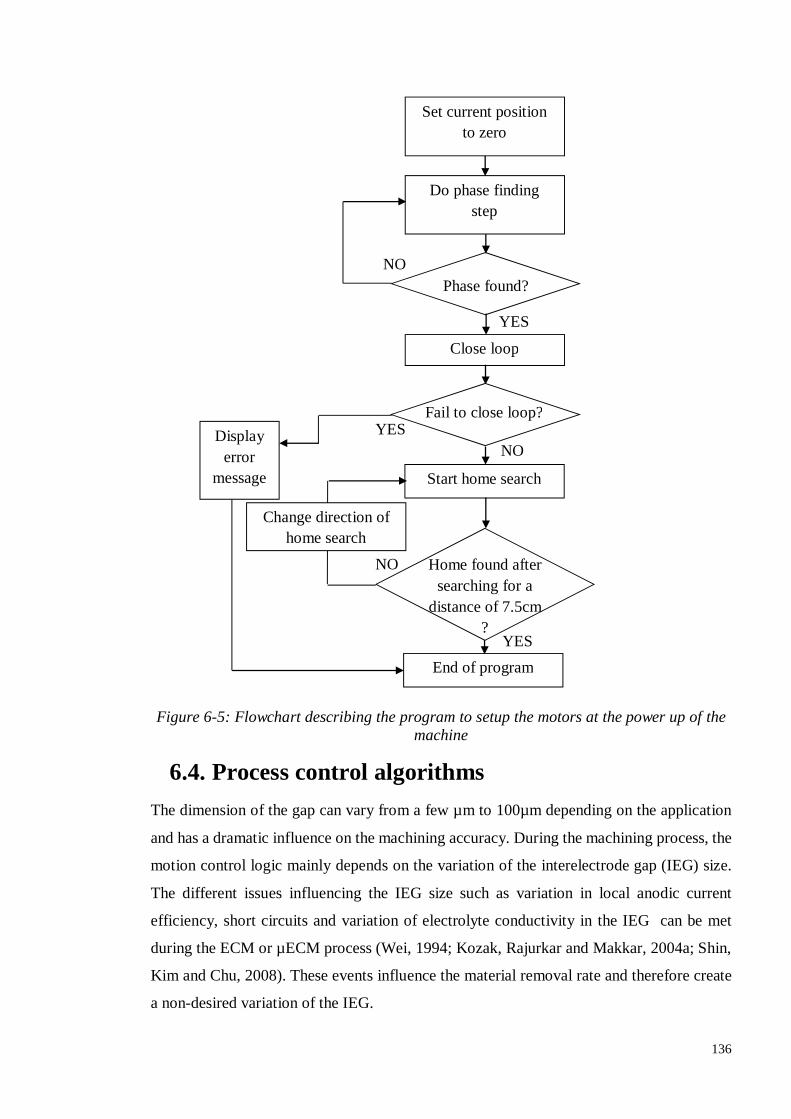
136
Figure 6-5: Flowchart describing the program to setup the motors at the power up of the machine
6.4. Process control algorithms The dimension of the gap can vary from a few µm to 100µm depending on the application
and has a dramatic influence on the machining accuracy. During the machining process, the
motion control logic mainly depends on the variation of the interelectrode gap (IEG) size.
The different issues influencing the IEG size such as variation in local anodic current
efficiency, short circuits and variation of electrolyte conductivity in the IEG can be met
during the ECM or µECM process (Wei, 1994; Kozak, Rajurkar and Makkar, 2004a; Shin,
Kim and Chu, 2008). These events influence the material removal rate and therefore create
a non-desired variation of the IEG.
Phase found?
Set current position to zero
Do phase finding step
YES
Close loop
NO
YES
Start home search
NO Home found after searching for a
distance of 7.5cm ?
YES End of program
Change direction of home search
Fail to close loop?
NO Display
error message

137
The process control algorithm is made of steps executed in a particular sequence
programmed using a state machine.
6.4.1. The state machine
The program running in the Power PMAC is a state machine containing all the different
actions necessary for the proper operation of the machine.
The state machine has the following main states:
SOFTSTOP: this state is triggered when a software problem happened during the
execution of a program on the PPMAC. It will automatically interrupt all the
programs running at the time the problem was detected.
SETUP: this state is used to setup the different parameters according to the values
sent by the HMI. It is also a stage at which all important variables are reset in order
to ensure proper machine operation.
TOUCH_N_GO: As its name suggests, in this state, a ‘Touch and go’ procedure is
performed. It consists of an algorithm which will determine the position of the
workpiece surface and then initialise the IEG.
FIND_WIRE: This state runs an algorithm similar to the one in the TOUCH_N_GO
state. The aim of this algorithm is to determine the position of the wire before
performing and electrochemical turning session for micro tool fabrication.
MEASURE_CURRENT: This state is necessary to measure the current flowing
through the gap at the beginning of machining. It will help setup the current target
for the fuzzy logic controller.
MACHINING: In this state, the electrochemical machining process is being
performed. This state is made of a state machine to react to unexpected events such
as short-circuits.
IDLE: The machine does not perform any task in this state, this is a ‘waiting’ state.
ESTOP: The machine goes in this state when the emergency stop button is pressed.
Pressing the ESTOP button will abort all programs and switch-off the power of the
amplifiers, therefore stopping any dangerous motion.

138
Figure 6-6: Flow chart of the main control programme running on the µECM machine
PLCs written in PMAC script language run in parallel of the main control algorithm. The
roles of the PLCs nr. 2, 3 and 4 are to automate the setup of the motors, each motor is
automatically setup (phase finding step, then home searching routine) when the user clicks
on the button ‘Motor Setup’ of the human machine interface (HMI).
Another PLC (plc1) is taking care of sending relevant data to the HMI.
6.4.1. The gap initialisation algorithm
To define the inter-electrode gap the following approach is used: A small voltage is applied
to the electrodes of the electrochemical cell and the tool-electrode is moved towards the
workpiece until a short circuit is detected. When the short circuit occurs, the machine
switches to a different mode where it will search the exact position where contact has been
made. This stage is done by a state machine program which is described in the flowchart on
Figure 6-7. This method helps define the position of the workpiece surface with a precision
of 0.1µm or better. From this position, the tool is retracted by the initial gap distance, which
is set to 5µm by default but it could be user specified.
IDLE
TOUCH_N_GO
SOFSTOP
SETUP
MACHINING
TOUCH_N_GO
FINDWIRE
ESTOP
Emergency stop button pressed
WIRE FOUND
Conditions to stop machining met or error
encountered
Emergency stop button pressed
Emergency stop button pressed Wire or workpiece surface found.
Setup finished Conditions to stop machining not met.
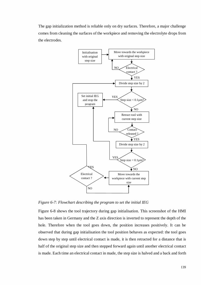
139
The gap initialization method is reliable only on dry surfaces. Therefore, a major challenge
comes from cleaning the surfaces of the workpiece and removing the electrolyte drops from
the electrodes.
Figure 6-7: Flowchart describing the program to set the initial IEG
Figure 6-8 shows the tool trajectory during gap initialisation. This screenshot of the HMI
has been taken in Germany and the Z axis direction is inverted to represent the depth of the
hole. Therefore when the tool goes down, the position increases positively. It can be
observed that during gap initialisation the tool position behaves as expected: the tool goes
down step by step until electrical contact is made, it is then retracted for a distance that is
half of the original step size and then stepped forward again until another electrical contact
is made. Each time an electrical contact in made, the step size is halved and a back and forth
YES
Move towards the workpiece with current step
size
Electrical contact ?
NO
Set initial IEG and stop the
program
Initialisation with original
step size
Step size < 0.1µm?
YES
Divide step size by 2
NO
NO
Contact
released ?
Retract tool with current step size
YES
Divide step size by 2
Move towards the workpiece with original step size
NO Electrical contact ?
Step size < 0.1µm? YES
YES
NO

140
motion is done. This process takes place until the step size reaches 0.1µm, giving a sufficient
degree of precision for the workpiece surface position. After the surface position has been
determined, the tool is moved backwards for a distance corresponding to the gap size.
Figure 6-8: Gap initialization, tool trajectory in Z axis
6.4.2. Machining process control algorithms
Different control approaches have been experimented in the past (Spieser and Ivanov, 2013)
and for this project 2 control strategies have been developed.
The machining process control algorithm is executed when the MACHINING state of the
main state machine described in section 6.4.1.
This algorithm also consists of a state machine in which two different control methods are
embedded.
6.4.2.1. IEG control using fuzzy logic
The first control algorithm consists of the use of a fuzzy controller to adjust the IEG
according to a desired machining current. The use of this approach for the ECM processed
was pointed out by Labib et al. (2011) who highlighted the necessity for the controller to
have decision making capabilities. Since the PECM process is very hard to mathematically
model, conventional control approaches such as proportional-integral-derivative (PID) or
state space controllers are limited and based on the linearisation of the process function (and
therefore approximation). They observed that the occurrence of sparking was efficiently
prevented when fuzzy logic control (FLC) was applied to the ECM process and encouraged
further research to develop FLCs for the EMM process. Moreover, it is worth mentioning
that fuzzy logic was also used to control the process in EDM, Wire-EDM (Çaydaş, Hasçalık
Gap initialization First electrical contact

141
and Ekici, 2009; Lin, Chung and Huang, 2001) and Electro-Chemical Discharge Machining
(ECDM) (Mediliyegedara et al., 2005; Skrabalak, Zybura-Skrabalak and Ruszaj, 2004).
Fuzzy logic has been introduced in the 1960’s and allows nonlinear functions to be modeled.
The fuzzy logic concept is based on the fact that in the real world something might not be
entirely TRUE or entirely FALSE as suggested by Boolean Logic.
The control algorithm consists of a fuzzy logic algorithm embedded in a state-machine
allowing it to react to unexpected events such as short circuits. The logic of the algorithm is
based on monitoring and maintaining a constant current through the inter-electrode gap. The
position of the tool electrode is controlled with respect to the variation between the desired
value of the machining current and its actual value. The type of the developed fuzzy logic
control algorithm is Takagi-Sugeno.
The input of the fuzzy logic controller is ‘mapped’ into different sub-levels. The
membership of the input variable with respect to these sub-levels is defined thanks to
functions called ‘membership functions’ that will help the controller determine to which of
the sub-levels the input belongs to. Therefore, a fuzzy logic controller deals with the degrees
of memberships of the variables it has to control (Labib et al., 2011). The output variable is
then adjusted according to the degree of membership of the input variable thanks to a rule-
based process. The definition of the rules is based on human knowledge and experience.
This provides the controller with a human decision-making capability.
The controller has two inputs:
1. The value of the measured current
2. The state of the PSU: pulsing (ON) or not pulsing (OFF)
The state of the over current protection signal is not taken into account here because a special
retraction routine has been implemented to handle short circuits and tool protection.
The fuzzy logic functions were developed in C and are based on a heavily modified version
of the Matlab fuzzy.c standalone fuzzy inference system. Indeed, the original C programme
reads parameters from a text file, which is not suitable for our application since the Power
PMAC does not run the HMI programme via which the user inputs their data. The way the
developed programme handles the fuzzy parameters has been made very dynamic, allowing
it to change its fuzzy rules on the fly.

142
The fuzzy logic inference system is fully integrated in the main routine controlling the
process; constantly monitoring the current at a sample rate of 1 kHz and adjusting the tool
position every 0.4s.
Input membership functions
For illustration purposes, the fuzzy logic controller was first simulated using Matlab’s Fuzzy
logic Toolbox.
Figure 6-9: Block diagram representation of the fuzzy logic controller on Matlab
The membership functions for the input variables have to be defined. Two types of
membership functions are used to define the input variables:
1. Trapezoidal membership function
The trapezoidal membership is configured thanks to 4 parameters: a, b, c and d.
a and d are used to define the ‘base’ of the trapezoid whereas b and c are used to define the
‘shoulders’ (Figure 6-10).
The formula of the trapezoidal membership function trapmf(x, a, b, c, d) is (Mathworks,
2014a):
trapmf(x, a, b, c, d) = max (minx − ab − a , 1,
d− xd− c , 0) (6-1)

143
Figure 6-10: Example of trapezoidal membership function (Mathworks, 2014a)
2. Triangular membership function
The trapezoidal membership is configured thanks to 3 parameters: a, b and c.
a and c are used to define the ‘base’ of the trapezoid whereas b is used to define the ‘summit’
(Figure 6-11).
The formula of the trapezoidal membership function trimf(x, a, b, c) is (Mathworks, 2014b):
trimf(x, a, b, c) = max (minx − ab − a ,
c − xc − b , 0) (6-2)
Figure 6-11: Example of triangular membership function (Mathworks, 2014b)
The value of the input variable ‘Current’ is divided into 3 ‘levels’ represented by 3
membership functions:
1. LowCurrent: this membership function is trapezoidal
2. OptimalCurrent: this membership function is triangular
3. HighCurrent: this membership function is trapezoidal

144
Figure 6-12: Defined membership functions for the input variable ‘Current’
The value of the input variable ‘PSUStatus’ is divided into 2 ‘levels’ represented by 2
membership functions:
1. ON: this membership function is triangular with [a,b,c] = [1,1,1]
2. OFF: this membership function is triangular with [a,b,c] = [0,0,0]
Figure 6-13: Defined membership functions for the input variable ‘PSUStatus’
Output membership function
Once the inputs have been defined, the output has to be configured. The output of the fuzzy
logic controller is called ‘SpeedCoef’, it is a coefficient of which the value is ranging from
-1 to 1. ‘SpeedCoef’ is multiplied by the maximum step length that can be achieved by the
controller in one step.
Definition of the membership functions for the output variable SpeedCoef: ‘SpeedCoef’
determines the direction and amplitude of the step move that will be performed.
In the Sugeno-type fuzzy controller, the output is defined by constant membership
functions:

145
1. Reverse: SpeedCoef is set to -1 2. Optimal: SpeedCoef is set to 0 3. Forward: SpeedCoef is set to 1
The rules determining the behaviour of the fuzzy logic controller can be seen below:
RULE #1: If current is ‘low’ AND Psu is ‘ON’ then Relative position is ‘forward’ RULE #2: If current is ‘low’ AND Psu is ‘OFF’ then Relative position is ‘nochange’ RULE #3: If current is ‘optimal’ AND Psu is ‘ON’ then Relative position is
‘nochange’ RULE #4: If current is ‘optimal’ AND Psu is ‘OFF’ then Relative position is
‘nochange’ RULE #5: If current is ‘high’ AND Psu is ‘ON’ then Relative position is
‘backwards’ RULE #6: If current is ‘high’ AND Psu is ‘OFF’ then Relative position is ‘nochange’
There are two ways of configuring the fuzzy logic controller and setting up the membership
function parameters:
1. Manually entering the values of the Maximum, Minimum and Optimal machining
current in the HMI:
Figure 6-14: The machining current setup tab in which the current parameters can be entered
2. Waiting for the gap to be initialized, start the electrolyte supply by turning on the
pump and pressing the button ‘MEASURE CURRENT’.
Pressing this button will make the PSU pulse for a short time during which the
current will be measured by the Power PMAC. The value of the measured current
will be assigned to the Optimal Current value (Opt_Current_Val) because it
corresponds to the current flowing through the gap at the initial gap. From this value

146
the maximum and minimum machining current values (Min_Current_Val and
Max_Current_Val) are computed as follows:
Min_Current_Val = Opt_Current_Val × 0.5
Max_Current_Val = Opt_Current_Val × 1.5 (6-3)
6.4.2.2. Adaptive feed rate algorithm
This control algorithm has been developed in order to adapt the tool feed rate according to
parameters calculated throughout the machining time:
Number of OCP events
Times and positions at which the OCP events occurred
Overall feed rate of the tool (calculated by using the start position, the current
position and the elapsed machining time)
Instantaneous feed rate (calculated after each step)
Approximation of MRR using the OCP times and positions
When the adaptive feed rate algorithm has enough data to influence the feed rate, it activates
itself.
This algorithm assumes that the positions and times at which the short circuits occur can be
used to calculate and adapt the feed rate. In the following illustration Figure 6-15, the
positions and times at which the short circuits occurred are stored in the Power PMAC.
Not all the short-circuits can be used to calculate the new feed rate of the tool: a filtering
mechanism is used to filter out and ignore the consecutive short-circuits positions and times
in order to only use representative data.
As soon as two representative short circuits have been gathered, the first feed rate can be
calculated using the formula:
OCPFeed rate =Short circuit position − Short circuit position
Short circuit time − Short circuit time (6-4)
All the calculated feed rates are stored in an array and the average of all the feed rates is
computed in order to obtain a more reliable result.
AvgOCPFeed rate =∑ OCPFeed rate
n (6-5)

147
The ratio between the current feed rate and the computed feed rate is calculated and the feed
rate is adjusted by the following operation:
FRCoef
= ((1 − α) × InitialFR + α× 0.5 × AvgOCPFR + α ∗ 0.5 ∗ Last3OCPFR)
InitialFR
(6-6)
Where α = if β < 10 or α = 1 otherwise. β represents the number of representative
short-circuits. The above expression considers that after 10 short circuits the value of
AvgOCPFR enables precise calculation of the desired feed rate and therefore the influence
of the initial feed rate can be neglected. This expression prevents the feed rate from being
reduced too quickly and assumes an increasing degree of confidence when more data is
gathered. This expression also takes into account the feed rate values calculated for the last
3 short circuits through the use of Last3OCPFR. It can be seen that the weight of
Last3OCPFR is the same as AvgOCPFR. Since the µECM process is long, providing the
controller with recent data is important and this is why Last3OCPFR has been integrated
into the formula.
Figure 6-15: Illustration of the adaptive feed rate algorithm
-34,9
-34,8
-34,7
-34,6
-34,5
-34,4
-34,3
0 10 20 30 40 50 60
Z Po
sitio
n (m
m)
Machining time (s)
Evolution of the tool position
Hole 3 Hole 5
First short circuits Second short
circuits
Deduced feed rates

148
6.4.2.3. Escape strategy
The process control algorithm consists of a state machine which reacts to the unpredictable
occurrence of short circuits during machining. In normal operation, the values of the signals
‘OCP’ and ‘PSU ON’ are checked to verify that no problem has been encountered. If
everything is fine (when the PSU is pulsing and the OCP has not been triggered), the
controller reads the value of the current on one of the channels of the data acquisition board
and computes the appropriate step size necessary to maintain the interelectrode gap to a
constant value. Controller constantly loops into that step unless an over current protection
signal is triggered or the PSU stops pulsing. If the PSU stops pulsing, the controller
interrupts the program and displays an error message on the HMI.
On the other hand, if an OCP event occurs (short circuit situation), the controller will switch
to a state which retracts the tool, restarts the power supply and goes back to the state of
fuzzy logic or adaptive control.
The retraction of the tool can be simple or in two steps according to the value of the global
variable gRetractBackNForward:
If the Power PMAC motion controller is configured for the simple tool retraction
(gRetractBackNForward set to 0), the tool will be retracted by a distance of which
the value is stored in the variable DesRetractDistance.
If gRetractBackNForward is set to 1 then the tool will be retracted by the user-
defined distance DesRetractDistance and then repositioned at a relative position –
creating a zone of turbulence in the electrolyte - defined by ResetPosition, defined
by:
ResetPosition = DesRetractDistance - (Consecutive_OCP_Counter+1) × InitialGap;
Consecutive_OCP_Counter represents the amount of short circuits that have
occurred consecutively. Short circuits are considered as consecutive if the time
period between their occurrences is less than 5seconds. According to the above
formula, the bigger the number of consecutive short circuits, the further away from
the surface the tool is repositioned. This algorithm has proven to be very efficient in
decreasing the number of short-circuits. The first retraction of the tool creates some
local electrolyte turbulence which eases the renewal of the electrolyte in the area

149
where the short circuit occurred. Replacing the tool at distances that are multiples of
the gap size enables a better gap control and more efficient machining than with the
simple retraction previously described.
The retraction code and graph illustrations can be seen in Figure 6-16.
Since the Power PMAC did not have the necessary drivers to communicate with the
microcontroller on the PSU, the communication between the PSU and the Power PMAC is
achieved via the HMI. However, when the over current protection is triggered and the
pulsing parameters do not need to be changed, the Power PMAC can trigger a restart of the
PSU using the 4 digital I/O ports that have been implemented on the PSU.
The communication protocol to reset the PSU is as follows:
The Power PMAC detects the OCP signal is high, so it retracts the tool for a predetermined
distance. Once the retraction move is performed, it sets one of the outputs connected to the
PSU inputs to a HIGH state. The PSU detects this action via one of its inputs and sets one
of its outputs to HIGH as an acknowledgment sign. The power PMAC then sets his output
to LOW to confirm it has received the signal. The PSU now resets the over current
protection and sets its output to LOW. The controller then carries on the machining program
until another unexpected event occurs.
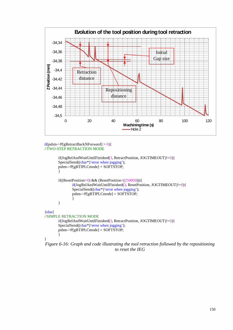
150
if(pshm->P[gRetractBackNForward] > 0){ //TWO-STEP RETRACTION MODE
if(JogRelAndWaitUntilFinished(3, RetractPosition, JOGTIMEOUT)!=0){ SpecialSend((char*)’error when jogging’); pshm->P[gRTIPLCmode] = SOFTSTOP; } if((ResetPosition>0) && (ResetPosition<(250000))){ if(JogRelAndWaitUntilFinished(3, ResetPosition, JOGTIMEOUT)!=0){ SpecialSend((char*)’error when jogging’); pshm->P[gRTIPLCmode] = SOFTSTOP; } }
}else{ //SIMPLE RETRACTION MODE
if(JogRelAndWaitUntilFinished(3, RetractPosition, JOGTIMEOUT)!=0){ SpecialSend((char*)’error when jogging’); pshm->P[gRTIPLCmode] = SOFTSTOP; } } Figure 6-16: Graph and code illustrating the tool retraction followed by the repositioning
to reset the IEG
-34,5
-34,48
-34,46
-34,44
-34,42
-34,4
-34,38
-34,36
-34,34
0 20 40 60 80 100 120
Z Po
sitio
n (m
m)
Machining time (s)
Evolution of the tool position during tool retraction
Hole 2
Initial Gap size
Retraction distance
Repositioning distance

151
6.5. An intelligent Human Machine Interface (HMI) A self-developed HMI connects directly to the motion controller (Power PMAC) and the
pulse PSU and allows the user to setup and monitor the machining current, tool position and
other essential machining parameters (Figure 6-17). This program has been written in C
using the CVI/LabWindows IDE from National Instruments. The communication protocol
used to connect with the Power PMAC is Telnet and the HMI is communicating to the PSU
via USB using a virtual COM port. The refresh time period of the displayed values has been
set to 150ms. The HMI also communicated with the spindle drive to set the rotation speed.
Figure 6-17: Screenshot of the self-developed HMI of the µECM machine
The HMI is a very important aspect of the machine: It not only displays relevant information
to the user, but also communicates with the PSU and the drive of the spindle.
Because of software driver issues, the Power PMAC cannot communicate with the PSU and
the spindle drive directly. Therefore the HMI is charged of communicating with these
components when the Power PMAC requests it.
The HMI reacts to some specific values that are sent by the Power PMAC, for example if
the controller wants to switch on the PSU, the global variable ‘gPSUCom’ is set to 1 and
sent to the HMI. The Power PMAC then waits for the PSU to switch within a certain time

152
lapse. If the elapsed time is too long, then the function times out and the Power PMAC puts
itself in a fail-safe mode by aborting any running program.
Also, if the connection between the HMI and the Power PMAC is interrupted for more than
2 seconds during machining, the Power PMAC stops instantly the ongoing programs.
After each machining session, the program automatically generates a machining report
containing all the parameters used for this particular session as well as all the current and
tool position values. These reports can also be generated at any time by pressing the ‘GEN.
REPORT’ button.
The HMI is made out of different Tabs which focus on particular aspects of the machine:
The Power PMAC (PPMAC) System Terminal: this tab (Figure 6-18) allows the
user to interact with the firmware of the Power PMAC motion controller. This is an
integrated Telnet client which allows the user to send commands to the controller.
Figure 6-18: Picture of the ‘PPMAC System Terminal’ tab of the HMI
The Controller Terminal: this tab (Figure 6-19) allows the user to see what actions
that the programs on the machine are currently executing. For example, if an OCP
event occurs, this will be printed out in this dialog box.

153
Figure 6-19: Picture of the 'Controller Terminal' tab of the HMI
The Analog/Digital Inputs/Outputs (A/D I/Os): this tab (Figure 6-20) reports the
status and voltage values acquired by the digital I/O board (ACC65E) and analogue
input board (ACC36UK). The ACC65E is configured so that it has 24 digital inputs
and 24 digital outputs. On the other hand the ACC36UK features 16 acquisition
channels.
Figure 6-20: Picture of the 'A/D IOs' tab of the HMI
The Motion tab: this tab (Figure 6-21) focuses of the motion aspects of the machine,
it contains information regarding the status of each motors and allows the user to
reset, start homing search and jog for each of the 3 linear motors of the machine.

154
Figure 6-21: Screenshot of the ‘Motion’ tab of the HMI
Machining Current Setup: this tab (Figure 6-22) enables the user to configure the
fuzzy logic controller in the ‘Current Regulation’ side of the tab. The operator sets
the maximum machining current, the optimal machining current and the minimum
machining current by inputting numerical values in the corresponding fields. These
values are used to calculate the membership functions necessary for the fuzzy logic
controller to operate.
The other parameters are related to the programming of the pulse PSU. From this
panel, the user can set the pulse shape (8 different choices available), the over current
protection (OCP), the duty cycle and the frequency. The button ‘PSU TOUCH &
GO SETTINGS’ makes another window appear to set the parameters of the PSU
used for the gap initialisation procedure.
Figure 6-22: Picture of the 'Machining Current Setup' tab of the HMI

155
Motion Parameter Setup: The user can set up the parameters for tool feed rate and
tool retraction using this tab (Figure 6-23).
The ‘maximum negative step’ as well as the ‘maximum positive step’ input field are
used to set the boundaries of the fuzzy logic controller’s output.
The value entered for the ‘OCP Retraction’ sets the distance for which the tool is
retracted when the over current protection is triggered.
The ‘Desired Depth’ parameter corresponds to the desired depth of the hole to be
machined and the feed rate of the tool will be set to 0 when the difference between
the ‘start’ and ‘stop’ positions reaches this value.
The parameters on the right hand side are related to the gap initialisation and
determine the initial speed at which the tool is being fed to touch the workpiece
(Forward length Gap Ini.) as well as the initial distance for which the tool is retracted
when electrical contact has been made (Retraction length at Gap Ini).
Figure 6-23: Picture of the 'Motion Parameter Setup' tab of the HMI
Spindle and Orbiting: this tab (Figure 6-24) contains parameters related to the
spinning and orbiting of the tool. The user can set the rotational speed of the spindle
as well as the spindle modes. The orbiting motion of the tool during machining can
be enabled and configured using the ‘Start Orbiting’ toggle switch and the Orbiting
radius/feed rate input fields respectively.
From this tab it is also possible to enable the adaptive feed rate algorithm which
changes the feed rate value according to the number of times the over current
protection is triggered.

156
Figure 6-24: Picture of the Spindle and Orbiting tab of the HMI
6.6. Conclusions In this Chapter, the control system programme was described in detail. The main challenge
was to setup the communication protocols between the different subsystems the PSU, the
Power PMAC and the PC running the HMI.
With the developed escape strategy the machine is able to control the interelectrode gap
very reliably and during long machining sessions. The different control strategies have been
explained and their efficiency was assessed in the experiments described in the next chapter.
Precise and detailed information about the control strategies used in ECM and µECM are
very hard to find in the literature. This chapter can therefore be regarded as a useful
contribution by providing insights and analysing what needs to be taken into consideration
when developing a control strategy for µECM.
The development of a custom-made HMI from scratch can also be considered as an
achievement and the source code that was written can be used as a framework for further
development with Power PMAC systems.

157
Chapter 7: EXPERIMENTAL WORK AND RESULTS This chapter presents the experimental work achieved during two different projects:
Experiments performed in Micro ECM project funded by the European commission
(work achieved in Sonplas)
Experiments performed at Brunel University in the frame of the European research
project MIDEMMA.
Preliminary drilling experiments with a test-bench can be read in 0.
The work presented in this chapter has been therefore performed on two different machines:
the machine at Sonplas uses components developed by other research partners such as the
pulse PSU from VOX Power. The author was responsible of the HMI and control systems
design on the machine in Sonplas.
On the other hand, the experiments at Brunel were performed using the machine described
in ‘Chapter 5: Machine system integration’ which has been developed by the author.
7.1. Experimental work at Sonplas GmbH on the machine developed in 2013 (Germany)
7.1.1. Discussion on the setup A series of tests have been undertaken to study the efficiency of the fuzzy logic control
strategy. The machined parts were made of the following materials: copper, 18NiCr6,
stainless steel, iron, chromium based alloys.
The HMI developed for the machine at Sonplas had to be adapted to the pulse PSU
developed by VOX Power. The research partners decided the use a round PCB with spring
probes to connect to PSU to the workpiece (Figure 7-1). The aim of this configuration was
to reduce the noise and the inductance of the connections by providing a Faraday cage.
The tool holder was then connected to the PSU using a slip ring in a conductive bath made
of galinstan. Galinstan is a liquid conductive metal and it was chosen instead of mercury for
safety reasons.
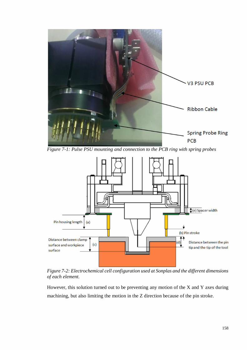
158
Figure 7-1: Pulse PSU mounting and connection to the PCB ring with spring probes
Figure 7-2: Electrochemical cell configuration used at Sonplas and the different dimensions of each element.
However, this solution turned out to be preventing any motion of the X and Y axes during
machining, but also limiting the motion in the Z direction because of the pin stroke.
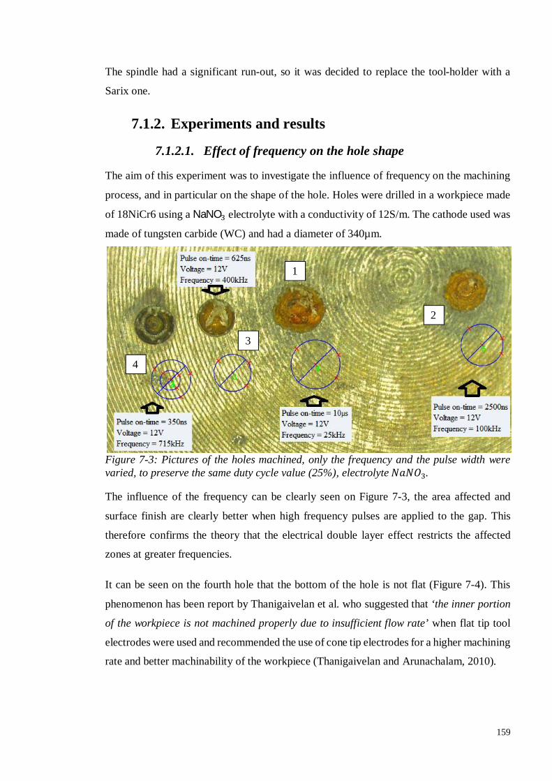
159
The spindle had a significant run-out, so it was decided to replace the tool-holder with a
Sarix one.
7.1.2. Experiments and results
7.1.2.1. Effect of frequency on the hole shape
The aim of this experiment was to investigate the influence of frequency on the machining
process, and in particular on the shape of the hole. Holes were drilled in a workpiece made
of 18NiCr6 using a NaNO electrolyte with a conductivity of 12S/m. The cathode used was
made of tungsten carbide (WC) and had a diameter of 340µm.
Figure 7-3: Pictures of the holes machined, only the frequency and the pulse width were varied, to preserve the same duty cycle value (25%), electrolyte 푁푎푁푂 .
The influence of the frequency can be clearly seen on Figure 7-3, the area affected and
surface finish are clearly better when high frequency pulses are applied to the gap. This
therefore confirms the theory that the electrical double layer effect restricts the affected
zones at greater frequencies.
It can be seen on the fourth hole that the bottom of the hole is not flat (Figure 7-4). This
phenomenon has been report by Thanigaivelan et al. who suggested that ‘the inner portion
of the workpiece is not machined properly due to insufficient flow rate’ when flat tip tool
electrodes were used and recommended the use of cone tip electrodes for a higher machining
rate and better machinability of the workpiece (Thanigaivelan and Arunachalam, 2010).
4
3
2
1

160
Figure 7-4: Profile of hole 4
7.1.2.2. Drilling with orbiting electrode
For these experiments, a 340µm-diameter WC tool-electrode was used. The electrolyte was
NaNO with a conductivity of 12S/m.
Our initial tests focused on determining the effect of different orbiting diameters. In all
instances the cathode was also rotating on its own axis as well orbiting.
The parameters were 12V pulse amplitude with a 500ns pulse on time and 500kHz (25%
duty cycle).

161
Figure 7-5: 1) 607m (right hole); 2) 596m (middle hole); 3) 505m (left hole)
Holes 1 and 2 had a 100µm orbiting radius set and hole 3 had an orbiting radius of 50µm.
The hole shape on 3 has a much better definition.
Hole 1 and 2 same parameters orbiting at 0.1mm similar depth and diameter. Process was
stable.
Although hole 3 was left to machine for a longer time, it can be seen that reducing the
orbiting offset from 0.1mm to 0.05mm resulted in a deeper hole and a smaller external
diameter (3 times deeper 178.4µm compared to 65.6µm and 60.4µm deep in 1 and 2
respectively).
This can be explained by the fact that when the tool is orbiting at a greater radius, the amount
of material to remove is bigger, so holes 1 and 2 are logically less deep than hole 3.
The value of the side gap at the top surface for each hole is:
(607-340-200)/2 = 33.5µm overcut for hole 1 (596-340-200)/2 = 28µm overcut for hole 2 (505-340-100)/2 = 32.5µm overcut for hole 3
If we approximate the volume of each tapered hole with the volume of a truncated cone,
the approximated volume of removed material for each hole is:
13615521.19 µm³ for hole 1, corresponding to a MRR of 0.0138mm³/min 12686968.96 µm³ for hole 2, corresponding to a MRR of 0.0147mm³/min 20611297.99 µm³ for hole 3, corresponding to a MRR of 0.0164mm³/min
The MRR was calculated by dividing the amount of volume removed by the machining time
displayed in Figure 7-7.

162
Figure 7-6: Profiles of the holes 1, 2 and 3
The MRR of the hole with a 0.05mm orbiting radius seems to be greater than those of the
holes with 0.1mm orbiting radius.
From the charts, the average machining current was 0.8A and the progression of the tool
was linear. The step size of the fuzzy control algorithm was kept constant for these three
tests. Since the amount of surface machined is bigger for holes 1 and 2, the tool was
progressing more slowly and more short-circuits occurs than for hole 3 (Figure 7-7).

163
Figure 7-7: Current and position charts for each of the holes drilled.
The short circuits occurred in a rather periodical pattern, which means that the MRR was
constant but that the feed rate set by the fuzzy logic controller was too high. This highlighted
the need for an adaptive feed rate algorithm to be developed.
Experiments showed that reducing the orbiting diameter has a clear impact on the hole
diameter and that rotation of the cathode as well as orbiting improves flushing and provides
a better hole shape.
7.1.2.1. Gasoline injector drilling
Tests were made on gasoline injectors provided by Magneti Marelli (Figure 7-9). These
parts are made of a chromium-based alloy which has an electrochemical behaviour similar
to the previously studied 18NiCr6 alloy. Holes were drilled using NaNO electrolyte and
12V pulses with a duty cycle of 25% and a frequency of 120 kHz.
The holes drilled in this experiment have a tapered shape due to the fact that the tool was
not side insulated and not orbiting during the machining process (Figure 7-10). Indeed, the
fact that the tool was not orbiting increased the number of short-circuits which slowed down
the progression of the tool.
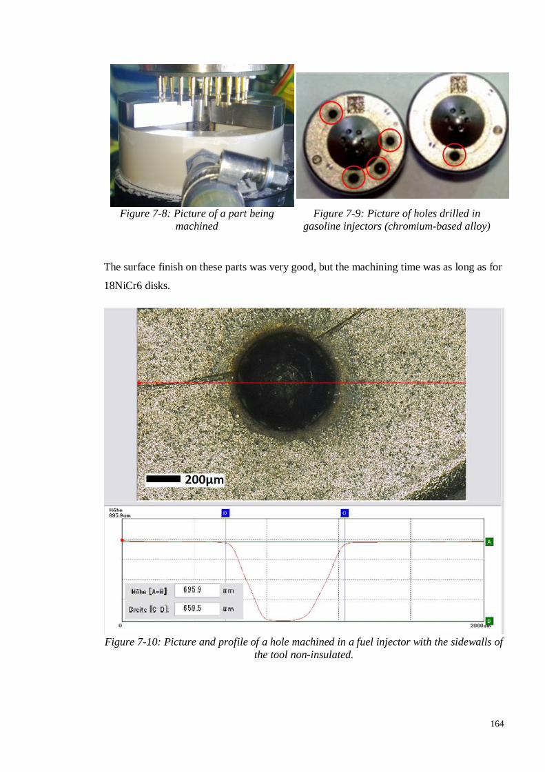
164
Figure 7-8: Picture of a part being machined
Figure 7-9: Picture of holes drilled in gasoline injectors (chromium-based alloy)
The surface finish on these parts was very good, but the machining time was as long as for
18NiCr6 disks.
Figure 7-10: Picture and profile of a hole machined in a fuel injector with the sidewalls of
the tool non-insulated.

165
7.1.2.1. Damaged electrodes due to sparking
Figure 7-11: A case of extreme tool-electrode wear when machining at 12V
It was often observed that during the drilling process the travel distance of the electrode
would not match the depth of the hole. An investigation concluded that pulses above 10V
would generate sparks and would damage the tool (Figure 7-11). The machining trials
therefore suggested that the machining voltage shall not be greater than 8V.
7.1.3. Process behaviour with the fuzzy logic control algorithm
The fuzzy logic algorithm behaved as expected: the algorithm was told to reach a target
value for the machining current and maintain it throughout the machining process.
However most of the machining tests were performed using non-insulated tool-electrodes,
so the sidewalls of the tool were conductive and taking part in the reaction. Since the process
was hole drilling, the active area of the tool would increase when the tool was fed. This
meant that the overall resistance of the machining gap was progressively reduces and that
more current was drawn by the IEG.
This resulted in the target current being reached very quickly, so the fuzzy logic controller
would reduce the feed rate to adapt to the change in current. Figure 7-12 illustrates perfectly
this phenomenon: at the beginning of the process, the tool progresses very quickly towards
the workpiece. Machining is taking place and the tool is fed forward, but then the current
increases because the side-walls are taking part in the reaction. The fuzzy logic controller
who had a machining current target of 1.5A would then reduce the feed rate of the tool when

166
the current value would reach 1.5A. On the picture it can be observed that the machining
current is very well regulated, with only a few short-circuits at the beginning of the process.
Figure 7-12: Machining result with the fuzzy logic control algorithm. Machining current
and tool position (Z) plotted over time (150ms per count)
The fuzzy logic controller regulated efficiently the machining current, but at the expense of
the machining feed rate, the cycle time was therefore not optimal. The machining was not
localized, because the tool was fed too slowly and the current passing through the side-walls
was increasing the side gap. This resulted in a long machining time with a big overcut.
7.2. Drilling experiments with orbiting tool-electrode Machining tests have been performed on workpieces made of 18NiCr6 alloys used in the
automotive industry which is hard to machine with conventional machining processes. The
machined part was a disk provided by the automotive component manufacturer Delphi UK.
The disk had a diameter of 1cm and was 1.1mm thick.

167
The use of many different types of electrolytes was reported in electrochemical machining.
For the experiments, NaNO mixed with a small amount of HCl was used as electrolyte. HCl
was combined with other chemicals in many papers (Lee, Baek and Cho, 2007; Sen and
Shan, 2005; Kirchner et al., 2001; Bilgi, Jain, Shekhar and Kulkarni, 2006; Trimmer et al.,
2003; Zemann et al., 2012; Mukherjee, Kumar and Srivastava, 2005; Mithu, Fantoni and
Ciampi, 2011a; Haisch, 2002; Zhang et al., 2007; Lu, Liu and Zhao, 2010; Cagnon et al.,
2003) in concentrations varying from 0.01M HCl (Trimmer et al., 2003) up to 3M HCl
(Cagnon et al., 2003). In this trial, the concentration of NaNO was 0.27mol/L, the measured
conductivity of the electrolyte was of 24.3mS/cm and its pH was 2.54, which corresponds
to 0.00284M HCl.
In this experiment, the reproducibility of the drilling process and the effect of orbiting tool-
electrode was evaluated. Nine holes were machined in the workpiece (Figure 7-13) and in
8 out of 9 trials the tool went through the workpiece. Hole number 4 is blind because of a
communication problem between the HMI and the PSU which stopped the machining
process. The adaptive feed rate algorithm was initialized at the beginning of the machining
session and the initial feed-rate was set to 0.5µm per sec. Moreover, in all those trials the
spindle was rotating at 600rpm. After machining all the holes, the workpiece was unclamped
for inspection. A thick and sticky black film seemed to have formed all over the workpiece
surface. It seemed like the overall surface was affected by the applied voltage.
The parameters for the machining process can be summarized in Table 7-1.
Hole number Parameters in the following order: Voltage, Frequency, Duty cycle, PSU Mode, Orbiting (Y/N) 1 6V, 1MHz, 15%, 2.3A, Mode 1, No 2 6V, 1MHz, 15%, 2.3A, Mode 1, No 3 6V, 1MHz, 15%, 2.3A, Mode 1, No 4 6V, 1MHz, 15%, 2.3A, Mode 1, No 5 6V, 1MHz, 15%, 2.3A, Mode 1, No 6 6V, 1MHz, 15%, 2.3A, Mode 1, No 7 6V, 50kHz, 15%, 2.3A, Mode 1, Yes: 50µm radius 8 6V, 1MHz, 15%, 2.3A, Mode 1, Yes: 50µm radius 9 6V, 1MHz, 15%, 2.3A, Mode 1, Yes: 50µm radius
Table 7-1: The different pulse PSU parameters and their respective range of values
It can be said from these results that the drilling charts (Figure 7-15) are very similar in
behaviour: at the beginning of the drilling process, it seemed difficult to remove material,
as a lot of short circuits took place (short circuits provoked the rapid tool retractions which
can be observed on the position chart), short circuits also occurred at this moment because

168
the adaptive feed rate algorithm was initialized and therefore had a limited effect. After a
few minutes, an optimal feed-rate was found by the algorithm and a linear progression was
observed. The algorithm resets itself periodically to verify if the optimal feed-rate has been
found and therefore some short circuits happen periodically until the feed-rate reaches an
appropriate value.
Figure 7-13: Picture of the workpiece after the electrochemical drilling process
(taken with a TESA Visio)
Figure 7-14: Evolution of the current peak value during the machining process. Each
point represents an average of 50 data points.
In almost all cases, when the depth of the hole approached 0.9mm it became more difficult
to remove material debris and a lot of short circuits were detected. The time necessary to
break through the work-piece seems to vary considerably from one workpiece to another.
0
0,2
0,4
0,6
0,8
1
1,2
1,4
0 200 400 600 800 1000 1200 1400 1600
Peak
cur
rent
val
ue (A
)
Machining time (s)
Evolution of the peak current value
Hole 1 Hole 2 Hole 3 Hole 5 Hole 6 Hole 7 Hole 8 Hole 9
7
9
8
6
5
4
3
2
1
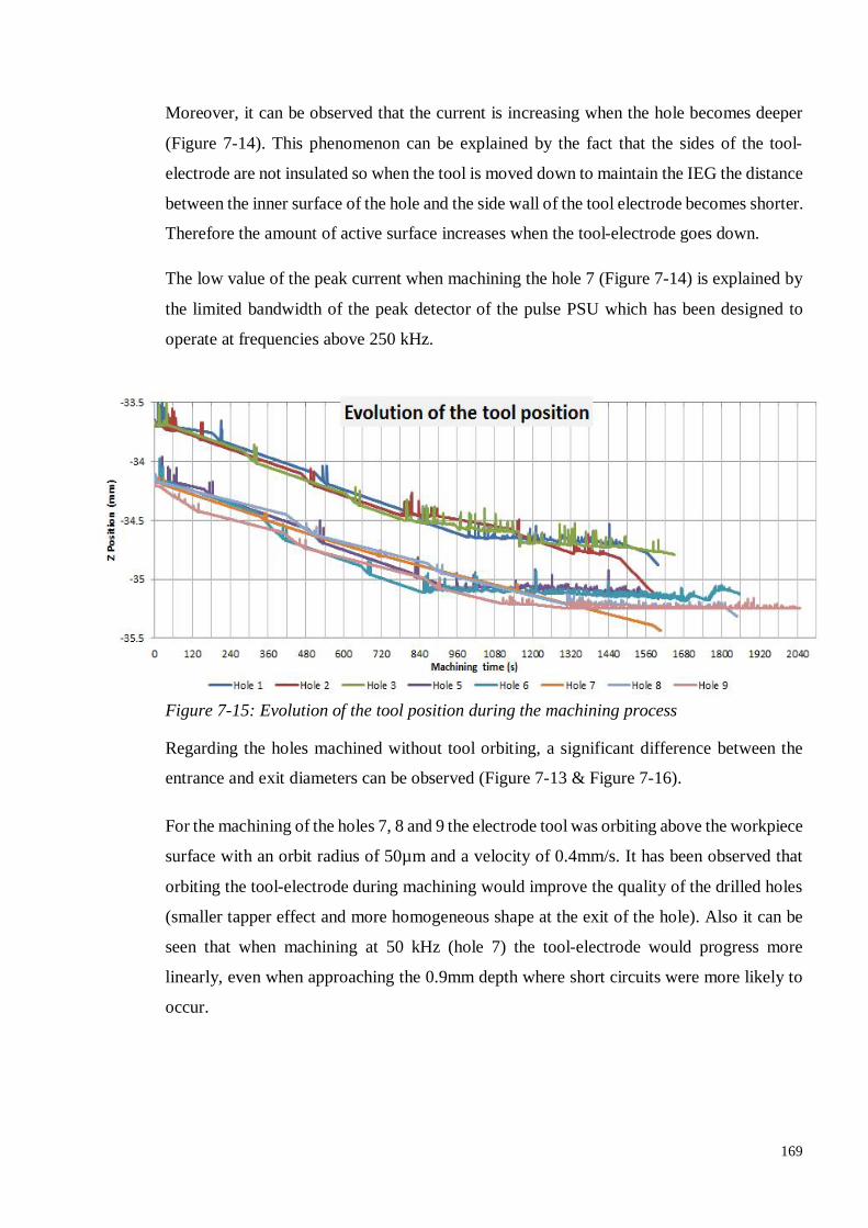
169
Moreover, it can be observed that the current is increasing when the hole becomes deeper
(Figure 7-14). This phenomenon can be explained by the fact that the sides of the tool-
electrode are not insulated so when the tool is moved down to maintain the IEG the distance
between the inner surface of the hole and the side wall of the tool electrode becomes shorter.
Therefore the amount of active surface increases when the tool-electrode goes down.
The low value of the peak current when machining the hole 7 (Figure 7-14) is explained by
the limited bandwidth of the peak detector of the pulse PSU which has been designed to
operate at frequencies above 250 kHz.
Figure 7-15: Evolution of the tool position during the machining process
Regarding the holes machined without tool orbiting, a significant difference between the
entrance and exit diameters can be observed (Figure 7-13 & Figure 7-16).
For the machining of the holes 7, 8 and 9 the electrode tool was orbiting above the workpiece
surface with an orbit radius of 50µm and a velocity of 0.4mm/s. It has been observed that
orbiting the tool-electrode during machining would improve the quality of the drilled holes
(smaller tapper effect and more homogeneous shape at the exit of the hole). Also it can be
seen that when machining at 50 kHz (hole 7) the tool-electrode would progress more
linearly, even when approaching the 0.9mm depth where short circuits were more likely to
occur.

170
Figure 7-16: Hole 5 diameter: Top:
0.432mm, Bottom: 0.221mm
Figure 7-17: Hole 7 diameter: 0.472mm
The tool electrode used in this experiment has a diameter of 170µm (Figure 7-19) and is
made of tungsten carbide (WC +5% Co). The best machining performance obtained in the
experiment is the hole nr. 9 (Figure 7-18) using the following machining parameters: 1MHz,
15% duty cycle, 2.3A OCP, orbiting of the tool with a 50µm orbit radius with a pulse
amplitude of 6V. The following pictures and diameter measurements have been taken with
a Tesa-Visio 200GL.
Figure 7-18: Hole 9, diameter: 0.394mm
Figure 7-19: Picture of the hole nr. 9 and the tool-electrode of a diameter of 175µm
orbiting with 50µm radius It can also be observed in Table 7-2 that the machining time of the hole number 9 was the
longest and resulted in a better result. The diameter for hole nr. 9 is 394µm. If we include
the orbiting radius and neglect the misalignment and run-out of the tool, the effective
diameter covered by the orbiting movement of the tool-electrode is 275µm, which
represents a 43% overcut. Moreover, the comparison between hole 7 (Figure 7-17) and hole
9 (Figure 7-18) shows that the use of lower frequency results in a less precise machining
and a rougher surface.

171
Hole number Entrance dia. (mm) Exit dia. (mm) Freq. Machining time (s) Orbiting
1 0.567 0.37 1MHz 1602 No 2 0.591 0.366 1MHz 1600 No 3 0.475 0.255 1MHz 1667 No 4 0.445 0.301 1MHz N/A No 5 0.432 0.221 1MHz 1536 No 6 0.451 0.317 1MHz 1855 No 7 0.472 0.472 50kHz 1602 Yes 8 0.44 0.44 1MHz 1843 Yes 9 0.394 0.394 1MHz 2043 Yes
Table 7-2: The different pulse PSU parameters and their respective range of values
7.3. Investigation on the effect of pulse frequency, duty cycle and voltage on the machining performance
7.3.1. Methodology The aim of this set of experiments was to analyse the influence of the machining parameters
(pulse frequency, duty cycle, and voltage) on the machining time and the side gap created
during the drilling of deep holes in 18NiCr6. The tool-electrode was made of WC-Co with
a diameter of 170µm and the electrolyte used was the same as in section 6.3: NaNO mixed
with a small amount of HCl with a conductivity of 24.3mS/cm.
The selected parameters are the following:
Level 1 2 3 Frequency Value (KHz) 250 500 1000 Duty Cycle (%) 15 30 45 Voltage (V) 5 7 9
Table 7-3: Selected parameter values for the experiment
3 main parameters have been identified and 3 different levels will be tested for most of
them, which results in an average number of levels close to 3.
According to the following array provided by Peter Woolf (Woolf, 2014), the array for
this experiment should be an L9 one.

172
Figure 7-20: Array used to determine which type of experimental array to use (Woolf, 2014)
Experiment Frequency (kHz) Duty Cycle (%) Voltage (V) 1 250 15 5 2 250 30 7 3 250 45 9 4 500 15 7 5 500 30 9 6 500 45 5 7 1000 15 9 8 1000 30 5 9 1000 45 7
Table 7-4: L9 Table of experiments to evaluate the influence of frequency
7.3.2. Results
Figure 7-21: Graph representing the evolution of the peak value of the current during machining time
-0,005
0,045
0,095
0,145
0,195
0,245
0,295
0,345
0,395
0 500 1000 1500 2000 2500 3000
Curr
ent (
A)
Machining time (s)
Evolution of the peak current value
Hole 1 Hole 2 Hole 3 Hole 4 Hole 5 Hole 7 Hole 8 Hole 9
Break-through pattern
Break-through patterns

173
A break-through pattern can be observed in the graphs Figure 7-21 and Figure 7-22: the
current decreases when the tool drills through the surface. This decrease in current can be
explained by the fact that the front face of the cathode is no longer active because the bottom
of the hole has been dissolved, so the only remaining active surfaces are the side walls. The
amount of active surface has therefore decreased so less current is flowing through the
system. Moreover, machining of the inner walls of the hole is still happening despite off the
tool having gone through because the sidewalls of the tool is not insulated; since the tool is
not moving in the X and Y directions, the side gap is increasing, which makes the current
decrease over time.
Figure 7-22: Graph representing the evolution of the tool position during machining
An overview of the resulting holes in the 18NiCr6 can be seen in Figure 7-23.
-36,3
-35,8
-35,3
-34,8
-34,3
0 500 1000 1500 2000 2500 3000
Z Po
sitio
n (m
m)
Machining time (s)
Evolution of the tool position
Hole 1 Hole 2 Hole 3 Hole 4 Hole 5 Hole 7 Hole 8 Hole 9

174
Figure 7-23: Overall picture of the workpiece used for the experiment
Figure 7-24: Experiment 1
Figure 7-25: Experiment 4
1 2 3
4 5 6
7 8 9

175
Figure 7-26: Experiment 6
Figure 7-27: Experiment 8
From the results of the experiments and by observing the above figures, it can be seen that
poor machining performance was observed for the following combination of parameters:
Experiment Frequency
(kHz) Duty Cycle
(%) Voltage (V) 1 250 15 5 4 500 15 7 6 500 45 5 8 1000 30 5
Table 7-5: Table of the parameters considered as non-optimal for the drilling of 18NiCr6 under the test conditions
It can be observed that all the experiments with a voltage set to 5V resulted in poor results
and therefore the voltage has a very important influence on the material removal rate.
Experiments 3, 5 and 9 presented the best results, the machining time was optimal and the
process resulted in well-shaped holes (Figure 7-28 to Figure 7-33). The influence of the
frequency can be observed by making a comparison between holes 3 and 9: hole 9 presents
sharper features, and almost no taper shape.
Experiment Frequency (kHz)
Duty Cycle (%) Voltage (V)
3 250 45 9 5 500 30 9 9 1000 45 7
Table 7-6: Table of the parameters considered as optimal for the drilling of 18NiCr6 under the test conditions.

176
Figure 7-28: Experiment 3: Hole entry
Radius: 290µm
Figure 7-29: Experiment 3: Hole exit
Radius: 223µm
Figure 7-30: Experiment 5: Hole entry
Radius: 248µm
Figure 7-31: Experiment 5: Hole exit
Radius: 208µm
Figure 7-32: Experiment 9: Hole entry
Radius: 193µm
Figure 7-33: Experiment 9: Hole exit
Radius: 185µm
Regarding the holes nr 2 and 7, the progression of the tool was slower than for holes 3, 5
and 9. However, the hole nr 7 showed very sharp edges and no taper shape. This is mainly
due to the high frequency and low duty cycle of the pulses.

177
Experiment Frequency (kHz)
Duty Cycle (%) Voltage (V)
2 250 30 7 7 1000 15 9
Table 7-7: Table of the parameters considered as medium for the drilling of 18NiCr6 under the test conditions.
Figure 7-34: Experiment 2: Hole entry
Radius: 255µm
Figure 7-35: Experiment 2: Hole exit
Radius: 189µm
Figure 7-36: Experiment 7: Hole entry
Radius: 196µm Figure 7-37: Experiment 7: Hole exit
Radius: 200µm
7.3.3. Discussion on the effect of pulse frequency, duty cycle and voltage on the machining performance
From the above results, it can be seen that the voltage has the strongest influence of the
process: no machining occurred below 7V, and 7V with 15% duty cycle was not enough to
remove material efficiently. The second most influential parameter is the duty cycle: the
combinations of parameter resulting in the fastest machining session had a duty cycle above
30%. The frequency had an influence on the resolution and the shape of the hole, but did
not influence the material removal rate as much as the duty cycle did.

178
The overcut presented in the results is not representative of the machining resolution: the
run-out of the spindle tool-holder is too significant to be ignored and was still visible despite
several attempts to reduce it. The same problems were observed on the machine developed
in Germany but it could be replaced by a Sarix precision tool-holder. The author suggests
the tool-holder to be changed in order to reduce the run-out.
7.3.4. Verification of the µECM LabVIEW simulation model
This section is a comparison between simulated and experimental results in section 3.6
‘Investigation on the effect of pulse frequency, duty cycle and voltage on the machining
performance’.
In order to assess if the results coming from the developed simulation programme were
realistic, the values of the simulated and actual material removal rates for the experiments
in section 3.6 were compared and the error between the two was calculated.
The volume of material removed during the simulation could be approximated to the volume
of a cylinder with the following expression:
V = (πr ) × h (7-1)
Where V is the volume of material removed in mm .
r is the radius (in mm) of the hole and h is the depth of the hole at the end of the
machining session (in mm).
The MRR is then calculated as follows:
MRR =V
T (7-2)
Where T is the total machining time (in s).
Machining parameters used for all simulations:
Current efficiency : 70% (when using NaNO3 electrolyte with current densities
higher than 20A/cm² according to Haisch, Mittemeijer and Schultze (2004).
Activation potential : 0.92V (Fe),
EDL capacitance : 1E F/mm²,
Kv : 0.0281mm /(A.s),

179
Conductivity : 0.00243 S/mm (NaNO3 electrolyte)
Experiment Frequency (kHz)
Duty Cycle (%)
Voltage (V)
Simulated MRR (mm /s)
Actual MRR
(mm /s)
Error (%)
1 250 15 5 1.010 E NA NA 2 250 30 7 2.008E 1.5642E 28% 3 250 45 9 2.933E 3.213E -8.71% 4 500 15 7 1.088E NA NA 5 500 30 9 1.931E 2.032E -4.97% 6 500 45 5 1.741E NA NA 7 1000 15 9 9.565E 3.517E 171% 8 1000 30 5 1.022E NA NA 9 1000 45 7 1.583E 1.502E 5.39%
Table 7-8: Comparison of the material removal rates (MRR) between the process simulations and the actual experiments
Figure 7-38: Screenshot of the resulting workpiece shape after the simulations.
In the experiments where the parameters were optimal for machining, the model error of the
simulation programme was below 10%.
When the parameters were not optimal and short-circuits occurred, the actual process took
longer than in the simulation and the material removal rate was reduced.
It can be concluded than when short-circuits occur, it is very hard to predict what the
material removal rate is going to be using the simulation software.

180
The simulation software can however be used to provide some insights to the operator and
the control system. The predictions are particularly accurate when the pulse duration is
above 450ns and the voltage is higher than 7V.
7.4. On-line tool fabrication followed by workpiece drilling
In these machining trials, a mixture of 0.1M H SO and 0.5M NaNO solutions has been
used as electrolyte.
The tool-electrode has a diameter of 170µm and is made of WC-Co alloy (WC +5% Co).
The workpiece was one disk made of 18NiCr6 alloy which was provided by the automotive
company Delphi UK. The disk is 1.1mm thick.
The positions of the surfaces of the wire and workpiece were determined by using the OCP
of the PSU. Setting the OCP to a very low threshold level allows the detection of the
electrical contact necessary to localize the surface and initialize the interelectrode gap.
The tool was first etched to a diameter of 105µm via Wire µECM (Figure 7-39) with the
following parameters: -7V pulses with no offset (pulse shape n°5), at a frequency of 2MHz
and 10% duty cycle (50ns pulses). Over current protection was set to 1A. The micro-tool
was spinning at 600rpm during the etching process and was slowly fed down towards the
wire while ultrashort pulses were delivered to the IEG. The wire was produced by
Agie/Charmilles and is commonly used for EDM, it had a diameter of 200µm and was made
of zinc.
The following pictures and diameter measurements have been taken with a Tesa-Visio
200GL.
After the tool was fabricated, a hole was drilled in the workpiece by reversing the polarity
of the pulses. A black film can be observed on the workpiece because of the carbide
compounds created during the machining of the 18NiCr6 alloys. This phenomenon is well-
known and was reported by Haisch et al. (Haisch, Mittemeijer and Schultze, 2004).

181
Figure 7-39: (a) Tool in the tool holder (b) Picture of the micro tip etched via Wire µECM (electrochemical turning), a 푁푎푁푂 salt layer can be observed along the tool surface (WC-Co alloy, electrolyte 0.5M 푁푎푁푂 + 0.1M 퐻 푆푂 , pulse amplitude: -7.5 V, pulse duration: 50 ns, pulse period: 500ns, feed rate: 0.3µm/s, diameter: 95µm).
Figure 7-40: Picture of the hole fabricated by ECM with the WC-Co etched tool. (a) hole entrance, (b) hole exit (18NiCr6 alloy, depth: 1.1mm, hole entrance diameter: 517µm, hole exit diameter: 414µm, electrolyte 0.5M 푁푎푁푂 + 0.1M 퐻 푆푂 , pulse amplitude: 8V, pulse duration: 250 ns, pulse period: 1 µs, feed rate: 0.3µm/s).
From the chart (Figure 7-41) it can be seen that the progression was rather linear, with a lot
of OCP retractions during the first half of the machining tests. This caused the current to
drop for a short amount of time, as it can be seen on the current chart. The process is
controlled by an algorithm which adapts the feed-rate of the tool according to the positions
and times at which the short circuits have occurred. The machining time was 3748s.

182
Figure 7-41: Graphs representing (a) the evolution of the current peak value of the pulses (in A) and (b) the evolution of the tool position (in mm) throughout the machining time (in s)
Figure 7-42: Oscilloscope screenshot of the measured pulses at the IEG during workpiece machining, 1MHz frequency, duty cycle of 25%, pulse amplitude of 8V and no offset during off-time 500ns/div.
0
0,05
0,1
0,15
0,2
0,25
0,3
0 400 800 1200 1600 2000 2400 2800 3200 3600
Peak
Cur
rent
Val
ue(A
)
Time (s)
Evolution of the current peak value of the pulses (A)
-28,85
-28,65
-28,45
-28,25
-28,05
-27,85
-27,65
0 400 800 1200 1600 2000 2400 2800 3200 3600
Tool
pos
ition
(mm
)
Time (s)
Evolution of Tool position (mm)
Tool retractions because of short-circuits
Current drops because of OCP triggering

183
7.5. Micro-Tool fabrication The pulse PSU was also used to machine micro-tools from WC-Co electrodes (170µm
diameter) via electrochemical turning.
A very sharp tool (Figure 7-43) was fabricated by repetitively scanning the surface of the
wire at a fixed gap. The tip of the tool measures 5µm. The machining of this tool was very
fast and took only 350 seconds.
Figure 7-43: Tool of the shape of a needle made by micro electrochemical turning. A non-machined tool-electrode of 170µm is placed next to it for size comparison. (WC-Co alloy, electrolyte 0.5M 푁푎푁푂 + 0.1M 퐻 푆푂 , pulse amplitude: -7.5 V, pulse duration: 50 ns, pulse period: 500ns, feed rate: 0.3µm/s, diameter: 95µm)
Another technique was applied to produce the tool seen in Figure 7-44. The smallest
diameter measured on that micro-tool is 46µm. The tip of the tool is slightly bigger and
measures 57µm. The side gap between the micro-tool and the wire was varied during the
machining process to achieve this curved tool shape. The aim of this experiment was to
fabricate a tool looking like a micro-probe used in CMM machines.
The surface was observed using optical equipment with the help of the National Physics
Laboratory (NPL). It was determined that the roughness of the machined WC-Co shaft in
Figure 7-44 was 120nm. In Figure 7-45 it can also be observed that the surface texture is
very uniform.
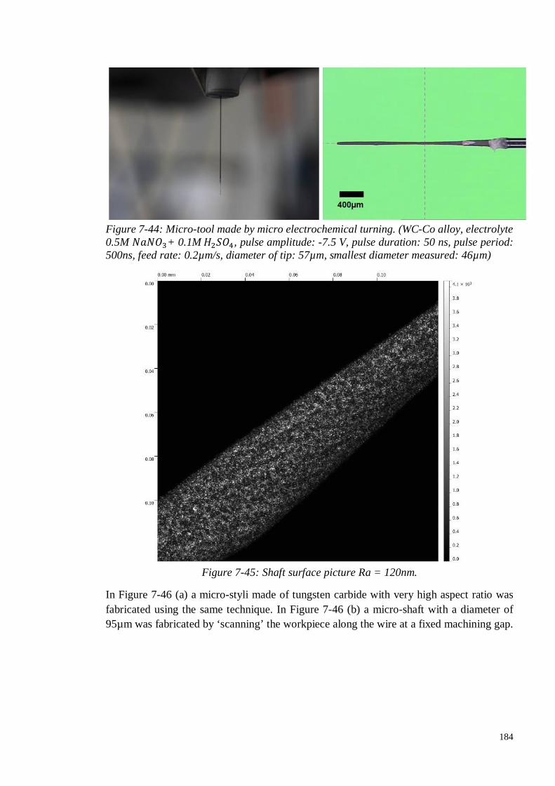
184
Figure 7-44: Micro-tool made by micro electrochemical turning. (WC-Co alloy, electrolyte 0.5M 푁푎푁푂 + 0.1M 퐻 푆푂 , pulse amplitude: -7.5 V, pulse duration: 50 ns, pulse period: 500ns, feed rate: 0.2µm/s, diameter of tip: 57µm, smallest diameter measured: 46µm)
Figure 7-45: Shaft surface picture Ra = 120nm.
In Figure 7-46 (a) a micro-styli made of tungsten carbide with very high aspect ratio was fabricated using the same technique. In Figure 7-46 (b) a micro-shaft with a diameter of 95µm was fabricated by ‘scanning’ the workpiece along the wire at a fixed machining gap.

185
Figure 7-46: (a) Micro-styli, diameter of tip: 45µm, smallest diameter measured: 32µm (b) Micro-shaft of 95µm diameter. (both made of WC-Co alloy with electrolyte 0.5M 푁푎푁푂 + 0.1M 퐻 푆푂 , pulse amplitude: -7.5 V, pulse duration: 50 ns, pulse period: 500ns, feed rate: 0.2µm/s)

186
Chapter 8: CONCLUSIONS AND FUTURE WORK
8.1. Conclusions In this work, a fully operational electrochemical micromachining machine was designed
and developed. The objectives defined at the beginning of this work have all been met.
(1) An extensive literature review provided insights on the state of the art development
in µECM and its research gaps.
The machine requirements for ultraprecision motion were identified, and it was
found that the use of air-bearings combined with DC brushless linear moter was
essential to achieve ultraprecision motion. A granite base was selected for its low
thermal expansion and a gantry configuration provided a very stable mechanical
structure.
For the motion control system, a 2-nm resolution encoder system was installed and
interfaced with the high-performance motion controller Delta Tau Power PMAC to
control the direct PWM drives.
This research concluded that the design and assembly of an innovative power supply
capable of delivering ultrashort pulses and providing enough power to the IEG was
needed in order to progress in the development of µECM equipment. Furthermore,
it implied that an ultrafast overcurrent protection should be integrated into the power
supply.
The trend in control systems for µECM seemed to go towards fuzzy logic and neural
networks, allowing manufacturers to put their knowledge into the system. Therefore
a special fuzzy logic control algorithm embedded in a state machine was first
developed to control the tool position during machining.
(2) The behaviour of the µECM process and the influence of the electrical double layer
have been modelled and simulated. The presented work is built over models found
in the literature review and provided an enhanced version of what was achieved so
far. The simulation programme provided realistic results and can be used to
determine optimum machining parameters.
The influence of conductivity and frequency on the localisation and the machining
time were analysed. It was concluded that for a same frequency, the lower

187
conductivity electrolyte exploited at best the EDL effect, providing an improved
localization.
However, a lower electrolyte conductivity and a higher pulse frequency would
increase the machining time. Therefore, a trade-off had to be made between the
localization of the machining and the cycle time.
(3) The design of a programmable power supply capable of delivering ultra-short pulses
and providing enough power to the IEG is essential in order to progress in the
development of µECM equipment.
In this work, a review for the pulse PSU requirements in µECM has been done and
a device meeting those requirements has been developed and tested. An ultra-fast
(50ns time delay) over current protection (OCP) system has been designed to protect
the tool against undesired events occurring within the interelectrode gap during
machining. The pulse PSU provides the control system with signals such as the
current peak value as well as the OCP signal, in order to quickly react and adapt the
motion of the tool. It is able to supply pulse with duration of 50ns at a frequencies
ranging from 1kHz to 5MHz, although it was found at above 2MHz, the material
removal rate dropped significantly.
The developed pulse PSU is also able to reverse its pulse polarity and add a
positive/negative biases during pulse off-time. This means that the µECM machine
is able to perform on-line tool fabrication as well as workpiece machining without
any intervention on the hardware (no need to change any cable connection). Pulse
PSUs with similar performance and functionalities have not been reported.
(4) A quick communication protocol between the power supply and the control system
was essential for the successful control of the µECM process. A special fuzzy logic
control algorithm embedded in a state machine was first developed to control the
tool position during machining.
With the developed escape strategy the machine is able to control the interelectrode
gap very reliably and during long machining sessions. The different control
strategies have been explained and their efficiency was assessed in the experiments.
The main findings resulting from the machining trials using the fuzzy logic strategy
were:

188
o The occurrence of sparking is efficiently prevented when fuzzy logic control
(FLC)
o There is a need to constantly update the rules to change the targeted
machining current when drilling with a tool-electrode of which the sidewalls
are not insulated.
o For the first time, fuzzy logic has been successfully applied to control a
µECM process.
The main findings resulting from the machining trials using the adaptive feed rate
control strategy were:
o The occurrence of sparking is efficiently prevented when the optimum tool-
electrode feed rate in reached.
o There is no machining underperformance linked to the tool feed rate,
resulting in a more efficient machining process.
The adaptive feed rate adapted rapidly the feed rate of the tool-electrode in order to
match the material removal rate. This resulted in a shorter machining time with
respect to the fuzzy logic control strategy. The progression of the tool-electrode was
linear and the occurrences of short-circuits were decreasing over time.
The adaptive feed rate algorithm provided with the most encouraging results. The
results presented show that fuzzy logic is a viable control method for maintaining
the inter-electrode gap throughout machining time although it is preferable to use
side-insulated cathode when using this control strategy.
(5) An intelligent of HMI to allow inexperienced users to communicate with the
machine was developed. The HMI allows the user to setup and monitor the
machining current, tool position and other essential machining parameters. The HMI
was fully integrated into the control system and was also responsible for
communicating with the spindle drive and pulse PSU on behalf of the controller. Its
source code can be used as a framework for further development with Power PMAC
systems. The HMI also reacts intelligently to values sent by the Power PMAC, and
suggests parameter values to the user for the fuzzy logic control system
configuration.
(6) The machine capabilities and applications have been investigated through
machining experiments including:

189
Drilling hole in 18NiCr6 disks
Fabricating micro styli and micro shafts
Fabricating micro needles
From these experiments it can be deduced that the shape of the hole is strongly
influenced by the drilling time, the tool spinning, the conductivity of the electrolyte
and the pulse frequency. The drilling time will have an influence on the diameter of
the hole but also on the tapper effect. It has been observed that orbiting of the tool
electrode with a small radius would enhance the machine performance and improve
the shape of the hole substantially.
It has been confirmed that a fine tuning of the pulse width and the scanning ratio
would ensure the localization of the dissolution process. The developed pulse PSU
was used to produce micro-tools and drill deep holes in 18NiCr6 with an on-line
fabricated tool. The results from the drilling in 18NiCr6 show that µECM is not
suitable for drilling applications in the automotive sector because of its long cycle
time compared to EDM. Nevertheless, the µECM process can be used as a post-
process step in order to improve the surface finish on parts machined by EDM.
On the other hand, the use of this µECM machine for the fabrication of micro-probes
targeting the CMM sector looks very promising.
The presented machine provides outstanding capabilities in terms of programmability and
motion precision. This research and development can lead to various applications such as
the drilling of micro-holes in hard to machine material for the metrology and medical
sectors.
8.2. Contributions to knowledge The development of this machine is associated by the following contributions to knowledge
in the µECM sector:
1) A thorough background research showing that the problems limiting full scale ECM
are the same as those being identified for µECM. This work contributed to the
overall knowledge by analysing the research challenges the µECM and ECM
industries are facing today and by identifying the gaps where further research in
needed.

190
2) The developed LabVIEW simulation programme provides the µECM sector with a
greater understanding of the process and is a step towards the development of an on-
the-machine simulation step before machining.
3) The innovative pulse PSU provides not only tens nanosecond order pulse duration,
but also plus and minus biases and a polarity switching functionality as well. It fulfils
the requirements of tool preparation with reversed ECM on the machine easily. The
careful design and implementation, integration with MCU, are of good references to
the researchers and engineers who work in micro ECM.
4) The machine configuration and PSU integration enabled an innovated and industry-
capable machining strategy consisting of a 2-step sequential method: a fully
automated on-line tool preparation followed by workpiece machining.
5) Two innovative interelectrode gap (IEG) control strategies were developed. Both of
these control approaches required the use of the developed pulse PSU featuring an
ultra-fast Over Current Protection (OCP):
i. The first one is the use of a fuzzy controller to adjust the IEG according to a
desired machining current.
ii. The second control strategy consists in the use of an adaptive machining
algorithm decreasing the tool-electrode feed rate according to the times and
positions at which short circuits are detected.
6) The experimental work in ‘Chapter 7: Experimental work and results’ described
µECM drilling trials in 18NiCr6 alloys, which were never published before. The
fabrication of micro-tools in tungsten carbide using wire µECM complements the
rare the literature describing this process.
This development can lead to various applications such as the drilling of micro-holes in hard
to machine material for the automotive and aerospace sectors. Each of these applications
will require the design of an adapted workpiece clamping system which should meet the
electrical and spatial requirements for an optimal machining performance (short current path
for high frequency, chemical resistant fixtures…).
Moreover, the machine can be used to fabricate micro-tools and micro-probes for the micro
coordinate measuring machine (micro-CMM) sector.
The author also strongly encourages the use of the µECM machine on hard to machine
materials such as indium antimonite (InSb).

191
8.3. Recommendations for future work This machine presents the first µECM prototype ever built in the UK. The author suggests
the following future work to be undertaken:
Improvement of the control system to allow the tool retraction when short-circuit
occurs during 3-axis motions.
Improvement of the tool clamping system to reduce the run-out and make the tool-
changing operation easier.
Development of a machine learning algorithm and comparison of performance with
the already existing control strategy.
Setup of a database to assist the operator in choosing the machining parameters
depending on the materials of the electrodes
Work on the pulse PSU to reduce the noise generated by the power semiconductors
during the turn-on and turn-off times.
Improvement of the workpiece clamping system to allow the installation of a piezo-
actuated machining cell in order to make the cell vibrate during machining.

192
REFERENCES Abuzied, H.H., 2012. Prediction of Electrochemical Machining Process Parameters using Artificial Neural Networks. 4(01), pp.125–132.
Ahn, S.H., Ryu, S.H., Choi, D.K. and Chu, C.N., 2004. Electro-chemical micro drilling using ultra short pulses. Precision Engineering, 28(2), pp.129–134.
Altena, H.S.J., 2004. EDM and ECM for mass production Philips DAP. Journal of Materials Processing Technology, 149(1-3), pp.18–21.
Altera, 2001. Application note 75: High-Speed Board Designs. (November), pp.1–18.
Analog Devices, 2010. Datasheet: AD8402: 2-Channel Digital Potentiometer. [online] Available at: <http://www.analog.com/static/imported-files/data_sheets/ AD8400_8402_8403.pdf> [Accessed 19 Apr. 2012].
Analog Devices, 2012. Datasheet: ADuM110 - iCoupler Digital Isolator. [online] Available at: <http://www.analog.com/static/imported-files/data_sheets/ADUM1100.pdf> [Accessed 17 Apr. 2013].
Anorad Linear Motor Division, U.S.. A., 1999. LE SERIES Motor Integration Manual LEA, LEB, LEC & LEM Linear Motors.
Ardizzoni, J., 2005. A Practical Guide to High-Speed Printed-Circuit-Board Layout. [online] Analog Dialog. Available at: <http://www.analog.com/library/analogdialogue/ archives/39-09/layout.pdf> [Accessed 14 Apr. 2013].
Asokan, P., Ravi Kumar, R., Jeyapaul, R. and Santhi, M., 2008. Development of multi-objective optimization models for electrochemical machining process. The International Journal of Advanced Manufacturing Technology, 39(1-2), pp.55–63.
Bähre, D., Weber, O. and Rebschläger, A., 2013. Investigation on Pulse Electrochemical Machining Characteristics of Lamellar Cast Iron using a Response Surface Methodology-Based Approach. Procedia CIRP, 6, pp.363–368.
Balogh, L., 2001. Design And Application Guide For High Speed MOSFET Gate Drive Circuits. In: Proc. Power Supply Design Seminar (SEM 1400). Texas Instruments.
Barbalace, A., Luchetta, A., Manduchi, G., Moro, M., Soppelsa, A. and Taliercio, C., 2008. Performance comparison of VxWorks, Linux, RTAI, and Xenomai in a hard real-time application. In: IEEE Transactions on Nuclear Science. pp.435–439.
Bhattacharyya, B., Doloi, B. and Sridhar, P.S., 2001. Electrochemical micro-machining: new possibilities for micro-manufacturing. Journal of Materials Processing Technology, 113(1-3), pp.301–305.

193
Bhattacharyya, B., Malapati, M. and Munda, J., 2004. Advancement in electrochemical micro-machining. International Journal of Machine Tools and Manufacture, 44(15), pp.1577–1589.
Bhattacharyya, B., Malapati, M. and Munda, J., 2005. Experimental study on electrochemical micromachining. Journal of Materials Processing Technology, 169(3), pp.485–492.
Bhattacharyya, B., Malapati, M., Munda, J. and Sarkar, A., 2007. Influence of tool vibration on machining performance in electrochemical micro-machining of copper. International Journal of Machine Tools and Manufacture, 47(2), pp.335–342.
Bhattacharyya, B. and Munda, J., 2003. Experimental investigation on the influence of electrochemical machining parameters on machining rate and accuracy in micromachining domain. International Journal of Machine Tools and Manufacture, 43(13), pp.1301–1310.
Bignon, C., Bédrin, C. and Weill, R., 1982. Application of Eddy Currents to the In-Process Measurement of the Gap in E.C.M. CIRP Annals - Manufacturing Technology, 31(1), pp.115–118.
Bilgi, D.S., Jain, V.K., Shekhar, R. and Kulkarni, A. V., 2006. Hole quality and interelectrode gap dynamics during pulse current electrochemical deep hole drilling. The International Journal of Advanced Manufacturing Technology, 34(1-2), pp.79–95.
Burkert, S., Schulze, H., Gmelin, T. and Leone, M., 2009. THE PULSE ELECTROCHEMICAL MICROMACHINING ( PECMM ) - SPECIFICATIONS OF THE PULSE UNITS -. International Journal of Material Forming, 2(1), pp.645–648.
Cagnon, L., Kirchner, V., Kock, M., Schuster, R., Ertl, G., Gmelin, W.T. and Kück, H., 2003. Electrochemical Micromachining of Stainless Steel by Ultrashort Voltage Pulses. Zeitschrift für Physikalische Chemie, 217(4-2003), pp.299–314.
Campbell, D., Harper, J., Natham, Vinodhkumar, Xiao, F. and Sundararajan, R., 2008. A Compact High Voltage Nanosecond Pulse Generator. In: Proc. ESA Annual Meeting on Electrostatics 2008. pp.1–12.
Çaydaş, U., Hasçalık, A. and Ekici, S., 2009. An adaptive neuro-fuzzy inference system (ANFIS) model for wire-EDM. Expert Systems with Applications, 36(3), pp.6135–6139.
Chang, D.-Y., Shen, P.-C., Hung, J.-C., Lee, S.-J. and Tsui, H.-P., 2011. Process Simulation–Assisted Fabricating Micro-Herringbone Grooves for a Hydrodynamic Bearing in Electrochemical Micromachining. Materials and Manufacturing Processes, 26(12), pp.1451–1458.
Cheng, K., 2008. Machining dynamics: Fundamentals, applications and practices. London: Springer.
Choi, S.H., Kim, B.H., Shin, H.S., Chung, D.K. and Chu, C.N., 2013. Analysis of the electrochemical behaviors of WC–Co alloy for micro ECM. Journal of Materials Processing Technology, 213(4), pp.621–630.
194
Choi, S.H., Ryu, S.H., Choi, D.K. and Chu, C.N., 2007. Fabrication of WC micro-shaft by using electrochemical etching. The International Journal of Advanced Manufacturing Technology, 31(7-8), pp.682–687.
Clark, W.G. and McGeough, J. a., 1977. Temperature distribution along the gap in electrochemical machining. Journal of Applied Electrochemistry, 7(4), pp.277–286.
Clifton, D., Mount, A., Alder, G. and Jardine, D., 2002. Ultrasonic measurement of the inter-electrode gap in electrochemical machining. International Journal of Machine Tools and Manufacture, 42(11), pp.1259–1267.
Van Damme, S., Hotoiu, E.L., Albu, C., Weyns, G., Deconinck, D. and Deconinck, J., 2011. Double Layer Effects in Computational Electrochemistry. In: The 219th ECS meeting.
Danilovic, M., Chen, Z., Wang, R., Luo, F., Boroyevich, D. and Mattavelli, P., 2011. Evaluation of the switching characteristics of a gallium-nitride transistor. In: 2011 IEEE Energy Conversion Congress and Exposition. IEEE, pp.2681–2688.
Data Delay Devices, 2008. Selection Guide - Pulse Generator & Oscillators. [online] Available at: <http://www.datadelay.com/datasheets/3d7622.pdf> [Accessed 15 Jul. 2014].
Datta, M. and Landolt, D., 1981. Electrochemical machining under pulsed current conditions. Electrochimica Acta, 26(7), pp.899–907.
Datta, M. and Landolt, D., 2000. Fundamental aspects and applications of electrochemical microfabrication. Electrochimica Acta, 45(15-16), pp.2535–2558.
Davydov, a. D., Volgin, V.M. and Lyubimov, V. V., 2004. Electrochemical machining of metals: Fundamentals of electrochemical shaping. Russian Journal of Electrochemistry, 40(12), pp.1230–1265.
Deconinck, D., Van Damme, S. and Deconinck, J., 2012a. A temperature dependent multi-ion model for time accurate numerical simulation of the electrochemical machining process. Part I: Theoretical basis. Electrochimica Acta, 60, pp.321–328.
Deconinck, D., Van Damme, S. and Deconinck, J., 2012b. A temperature dependent multi-ion model for time accurate numerical simulation of the electrochemical machining process. Part II: Numerical simulation. Electrochimica Acta, 69, pp.120–127.
Deconinck, J., 1992. Current Distributions and Electrode Shape Changes in Electrochemical Systems. Berlin, Heidelberg/New York: Springer-Verlag.
Delta Tau Data Systems, 2006. Installation Manual: Geo Direct PWM Amplifiers. pp.1–78.
Delta Tau Data Systems, 2009. USER MANUAL: Acc24E2 - Axis Expansion Board. (818).
Delta Tau Data Systems, 2011. User manual: Acc11E. (818).
ECMTEC GmbH, 2012. ECMTEC Website. [online] Available at: <http://www. ecmtec.com/> [Accessed 6 Aug. 2014].

195
EMAG, 2012. MicroECM Machine brochure EMAG. [online] Available at: <http://www.interempresas.net/FeriaVirtual/Catalogos_y_documentos/1163/EMAG-MicroECM-ingles.pdf> [Accessed 6 Aug. 2014].
EMAG GmbH, 2014. EMAG Website - ECM / PECM Machines. [online] Available at: <http://www.emag.com/machines/ecm-pecm-machines/cs-ci.html> [Accessed 6 Aug. 2014].
Fairchild-Semiconductor, 2009. FDMS7578 Power Trench N-MOSFET. [online] Available at: <http://www.fairchildsemi.com/ds/FD/FDMS7578.pdf> [Accessed 12 May 2013].
Fan, Z.-W. and Hourng, L.-W., 2011. Electrochemical micro-drilling of deep holes by rotational cathode tools. The International Journal of Advanced Manufacturing Technology, 52(5-8), pp.555–563.
Fan, Z.-W., Hourng, L.-W. and Lin, M.-Y., 2012. Experimental investigation on the influence of electrochemical micro-drilling by short pulsed voltage. The International Journal of Advanced Manufacturing Technology, 61(9-12), pp.957–966.
Floridor, G., Van den Bossche, B., Nelissen, G., Bortels, L. and Deconinck, J., 2004. Numerical investigation of transient current density distributions for multi-ion electrolytes at a rotating disk electrode. Analytical chemistry, 76(18), pp.5579–90.
Fujii, Y., Muramoto, Y. and Shimizu, N., 2010. Analysis of electric double layer in aqueous solutions of sodium chloride. 2010 Annual Report Conference on Electrical Insulation and Dielectic Phenomena, pp.1–4.
Gao, W., Arai, Y., Shibuya, A., Kiyono, S. and Park, C.H., 2006. Measurement of multi-degree-of-freedom error motions of a precision linear air-bearing stage. Precision Engineering, 30(1), pp.96–103.
Haisch, T., 2002. High rate electrochemical dissolution of iron- based alloys in NaCl and NaNO3 electrolytes. Max-Planck-Institut für Metallforschung Stuttgart.
Haisch, T., Mittemeijer, E. and Schultze, J.W., 2001. Electrochemical machining of the steel 100Cr6 in aqueous NaCl and NaNO3 solutions: microstructure of surface films formed by carbides. Electrochimica Acta, 47(1-2), pp.235–241.
Haisch, T., Mittemeijer, E.J. and Schultze, J.W., 2004. High rate anodic dissolution of 100Cr6 steel in aqueous NaNO3 solution. pp.997–1005.
Hocheng, H., Sun, Y.H., Lin, S.C. and Kao, P.S., 2003. A material removal analysis of electrochemical machining using flat-end cathode. Journal of Materials Processing Technology, 140(1-3), pp.264–268.
Hotoiu, E.L., Van Damme, S., Deconinck, D., Albu, C., Weyns, G. and Deconinck, J., 2011. Development of simulation software package for nano-pulsed electrochemical micro machining. In: The 219th ECS meeting.

196
Hotoiu, L., Van Damme, S. and Deconinck, J., 2011. Progress report PECMM simulations WP3-M4. pp.1–18.
Huang, S.H., Huang, F.Y. and Yan, B.H., 2004. Fracture strength analysis of micro WC-shaft manufactured by micro-electro-discharge machining. The International Journal of Advanced Manufacturing Technology, 26(1-2), pp.68–77.
Hui, C., Wang, Y.-K., Wang, Z.-L. and Zhao, W.-S., 2011. Effects of Complexing Agent on Electrochemical Micro Machining of Stainless Steel. American Journal of Nanotechnology, 2(1), pp.100–105.
Huo, D. and Cheng, K., 2008. A dynamics-driven approach to the design of precision machine tools for micro-manufacturing and its implementation perspectives. Proceedings of the Institution of Mechanical Engineers, Part B: Journal of Engineering Manufacture, 222(1), pp.1–13.
Huo, D., Cheng, K. and Wardle, F., 2010a. Design of a five-axis ultra-precision micro-milling machine-UltraMill. Part 1: Holistic design approach, design considerations and specifications. International Journal of Advanced Manufacturing Technology, 47, pp.867–877.
Huo, D., Cheng, K. and Wardle, F., 2010b. Design of a five-axis ultra-precision micro-milling machine-UltraMill. Part 2: Integrated dynamic modelling, design optimisation and analysis. International Journal of Advanced Manufacturing Technology, 47, pp.879–890.
IIT Kharagpur, 2014. Lesson 38. Electro Chemical Machining - Non-conventional Manufacturing processes. [online] Available at: <http://nptel.iitm.ac.in/courses/ Webcourse-contents/IIT Kharagpur/Manuf Proc II/pdf/LM-38.pdf> [Accessed 22 Sep. 2014].
Indec, 2014. Indec ‘ET’ ECM Machines. [online] Available at: <http://www.indec-ecm.com/en/equipment/ekp/ekp/ET500-1&ET1000-1/> [Accessed 26 Aug. 2014].
Intersil, 2010. Datasheet: EL5166 - 1.4GHz Current Feedback Amplifiers with Enable. [online] Available at: <http://www.intersil.com/content/dam/intersil/documents/ el51/el5166-67.pdf> [Accessed 12 Apr. 2013].
Jain, V.K. and Pandey, P.C., 1981. Tooling Design for ECM—A Finite Element Approach. Journal of Engineering for Industry, 103(2), p.183.
Jauregui, D., 2009. Reducing Ringing Through PCB Layout Techniques. Texas Instruments, pp.1–6.
Jo, C.H., Kim, B.H., Shin, H.S., Chung, D.K., Kwon, M.H. and Chu, C.N., 2008. Micro Electrochemical Machining for Complex Internal Micro Features. Internal Conference on Smart Manufacturing Application, pp.247–250.
Kamaraj, A.B. and Sundaram, M.M., 2013. Mathematical modeling and verification of pulse electrochemical micromachining of microtools. The International Journal of Advanced Manufacturing Technology.

197
Kamaraj, A.B., Sundaram, M.M. and Mathew, R., 2013. Ultra high aspect ratio penetrating metal microelectrodes for biomedical applications. Microsystem Technologies, 19(2), pp.179–186.
Kenney, J. a., Hwang, G.S. and Shin, W., 2004. Two-dimensional computational model for electrochemical micromachining with ultrashort voltage pulses. Applied Physics Letters, 84(19), p.3774.
Kim, B., Na, C., Lee, Y., Choi, D. and Chu, C., 2005a. Micro Electrochemical Machining of 3D Micro Structure Using Dilute Sulfuric Acid. CIRP Annals Manufacturing Technology, 54(1), pp.191–194.
Kim, B.H., Ryu, S.H., Choi, D.K. and Chu, C.N., 2005b. Micro electrochemical milling. Journal of Micromechanics and Microengineering, 15(1), pp.124–129.
Kirchner, V., Cagnon, L., Schuster, R. and Ertl, G., 2001. Electrochemical machining of stainless steel microelements with ultrashort voltage pulses. Applied Physics Letters, 79(11), p.1721.
Kock, M., Kirchner, V. and Schuster, R., 2003. Electrochemical micromachining with ultrashort voltage pulses–a versatile method with lithographical precision. Electrochimica Acta, 48(20-22), pp.3213–3219.
Kozak, J., 2001. Computer simulation system for electrochemical shaping. Journal of Materials Processing Technology, 109(3), pp.354–359.
Kozak, J., Dabrowski, L., Lubkowski, K., Rozenek, M. and Søawin, R., 2000. CAE-ECM system for electrochemical technology of parts and tools. Journal of Materials Processing Technology, 107(1-3), pp.293–299.
Kozak, J., Gulbinowicz, D. and Gulbinowicz, Z., 2008. The Mathematical Modeling and Computer Simulation of Pulse Electrochemical Micromachining. In: IAENG TRANSACTIONS ON ENGINEERING TECHNOLOGIES VOLUME 2: Special Edition of the World Congress on Engineering and Computer Science. San Francisco (CA): AIP Conf. Proc., pp.174–185.
Kozak, J., Rajurkar, K.P. and Makkar, Y., 2004a. Selected problems of micro-electrochemical machining. Journal of Materials Processing Technology, 149(1-3), pp.426–431.
Kozak, J., Rajurkar, K.P. and Makkar, Y., 2004b. Study of Pulse Electrochemical Micromachining. Journal of Manufacturing Processes, 6(1), pp.7–14.
Kozak, J., Rajurkar, K.P. and Ross, R.F., 1991. Computer Simulation of Puse Electrochemical Machining (PECM). Journal of Materials Processing Technology, 28, pp.149–157.
Labib, A.W., Keasberry, V.J., Atkinson, J. and Frost, H.W., 2011. Expert Systems with Applications Towards next generation electrochemical machining controllers : A fuzzy logic control approach to ECM. Expert Systems With Applications, 38(6), pp.7486–7493.

198
Landolt, D., Chauvy, P.-F. and Zinger, O., 2003. Electrochemical micromachining, polishing and surface structuring of metals: fundamental aspects and new developments. Electrochimica Acta, 48(20-22), pp.3185–3201.
Lee, E.S., Baek, S.Y. and Cho, C.R., 2007. A study of the characteristics for electrochemical micromachining with ultrashort voltage pulses. The International Journal of Advanced Manufacturing Technology, 31(7-8), pp.762–769.
Lee, E.S., Park, J.W. and Moon, Y.H., 2002. A Study on Electrochemical Micromachining for Fabrication of Microgrooves in an Air-Lubricated Hydrodynamic Bearing. International Journal of Advanced Manufacturing Technology, 20(10), pp.720–726.
Li, Z. and Ji, H., 2009. Machining Accuracy Prediction of Aero-engine Blade in Electrochemical Machining Based on BP Neural Network. In: Proceedings of the 2009 International Workshop on Information Security and Application (IWISA 2009) ISBN 978-952-5726-06-0. Qingdao, China: ACADEMY PUBLISHER, pp.9–12.
Lin, C.-T., Chung, I.-F. and Huang, S.-Y., 2001. Improvement of machining accuracy by fuzzy logic at corner parts for wire-EDM. Fuzzy Sets and Systems, 122(3), pp.499–511.
Linear Technology, 2014. LTC6903/LTC6904 - 1kHz to 68MHz Serial Port Programmable Oscillator. [online] Available at: <http://cds.linear.com/docs/Datasheet/69034fc.pdf> [Accessed 15 Jul. 2014].
Liu, Y., Zhu, D., Zeng, Y. and Yu, H., 2011. Development of microelectrodes for electrochemical micromachining. The International Journal of Advanced Manufacturing Technology, 55(1-4), pp.195–203.
Liu, Y., Zhu, D. and Zhu, L., 2012. Micro electrochemical milling of complex structures by using in situ fabricated cylindrical electrode. The International Journal of Advanced Manufacturing Technology, 60(9-12), pp.977–984.
Lu, X. and Leng, Y., 2005. Electrochemical micromachining of titanium surfaces for biomedical applications. Journal of Materials Processing Technology, 169(2), pp.173–178.
Lu, Y., Liu, K. and Zhao, D., 2010. Experimental investigation on monitoring interelectrode gap of ECM with six-axis force sensor. The International Journal of Advanced Manufacturing Technology, 55(5-8), pp.565–572.
Luo, X., Cheng, K., Webb, D. and Wardle, F., 2005. Design of ultraprecision machine tools with applications to manufacture of miniature and micro components. Journal of Materials Processing Technology, 167(2-3), pp.515–528.
Marla, D., Joshi, S.S. and Mitra, S.K., 2008. Modeling of electrochemical micromachining: comparison to experiments. Journal of Micro/Nanolithography, MEMS and MOEMS, 7(3), p.033015.
Masuzawa, T., Fujino, M., Kobayashi, K., Suzuki, T. and Kinoshita, N., 1985. Wire Electro-Discharge Grinding for Micro-Machining. CIRP Annals - Manufacturing Technology, 34(1), pp.431–434.

199
Mathew, R. and Sundaram, M.M., 2012. Modeling and fabrication of micro tools by pulsed electrochemical machining. Journal of Materials Processing Technology, 212(7), pp.1567–1572.
Mathworks, 2014a. Trapezoidal-shaped membership function. [online] Available at: <http://www.mathworks.co.uk/help/fuzzy/trapmf.html> [Accessed 14 Nov. 2013].
Mathworks, 2014b. Triangular-shaped membership function. [online] Available at: <http://www.mathworks.co.uk/help/fuzzy/trimf.html> [Accessed 14 Nov. 2013].
Maxim, 2007. Datasheet: MAX038, High-Frequency Waveform Generator. [online] Available at: <http://datasheets.maximintegrated.com/en/ds/MAX038.pdf> [Accessed 19 Apr. 2012].
McGeough, J.A., 1974. Principles of Electrochemical Machining. London: Chapman and Hall.
Mediliyegedara, T.K.K.R., Silva, a. K.M. De, Harrison, D.K. and McGeough, J. a., 2005. New developments in the process control of the hybrid electro chemical discharge machining (ECDM) process. Journal of Materials Processing Technology, 167(2-3), pp.338–343.
Meijer, J. and Veringa, J.C.M., 1984. Characteristic numbers to describe the detail transfer quality of electro-chemical machining. Precision Engineering, 6(2), pp.79–82.
Mithu, M. a. H., Fantoni, G. and Ciampi, J., 2011a. The effect of high frequency and duty cycle in electrochemical microdrilling. The International Journal of Advanced Manufacturing Technology, 55(9-12), pp.921–933.
Mithu, M.A.H., Fantoni, G. and Ciampi, J., 2011b. A step towards the in-process monitoring for electrochemical microdrilling. The International Journal of Advanced Manufacturing Technology, 57(9-12), pp.969–982.
Mithu, M.A.H., Fantoni, G., Ciampi, J. and Santochi, M., 2012. On how tool geometry, applied frequency and machining parameters influence electrochemical microdrilling. CIRP Journal of Manufacturing Science and Technology, 5(3), pp.202–213.
Muetze, A. and Oh, H.W., 2008. Design Aspects of Conductive Microfiber Rings for Shaft-Grounding Purposes. IEEE Transactions on Industry Applications, 44(6), pp.1749–1757.
Muir, R.N., Curry, D.R., Mill, F., Sherlock, A. and Mount, a R., 2007. Real-time parameterization of electrochemical machining by ultrasound measurement of the interelectrode gap. Proceedings of the Institution of Mechanical Engineers, Part B: Journal of Engineering Manufacture, 221(4), pp.551–558.
Mukherjee, S.K., Kumar, S. and Srivastava, P.K., 2005. Effect of Over Voltage on Material Removal Rate During Electrochemical Machining. 8(1), pp.23–28.

200
Mukherjee, S.K., Kumar, S. and Srivastava, P.K., 2007. Effect of electrolyte on the current-carrying process in electrochemical machining. Proceedings of the Institution of Mechanical Engineers, Part C: Journal of Mechanical Engineering Science, pp.1415–1419.
Narayanan, O.H., Hinduja, S. and Noble, C.F., 1986. The prediction of workpiece shape during electrochemical machining by the boundary element method. International Journal of Machine Tool Design and Research, 26(3), pp.323–338.
Nor, M.K.M., 2010. Development of the UMAC-Based Control System with Application to 5-Axis Ultraprecision Micromilling Machines. Brunel Univeristy.
NXP, 2014. UM10204 - I2C-bus specification and user manual. [online] Available at: <http://www.nxp.com/documents/user_manual/UM10204.pdf> [Accessed 21 Apr. 2013].
Oh, K.S., 2000. MOSFET Basics, Application Note AN9010. Fairchild Semiconductor, pp.1–37.
Owlad, M., Aroua, M.K., Daud, W.A.W. and Baroutian, S., 2009. Removal of Hexavalent Chromium-Contaminated Water and Wastewater: A Review. Water, Air, and Soil Pollution, 200(1-4), pp.59–77.
Ozkeskin, F.M., 2008. Feedback controlled high frequency electrochemical micromachining. Texas A&M University.
Park, B.J., Kim, B.H. and Chu, C.N., 2006. The Effects of Tool Electrode Size on Characteristics of Micro Electrochemical Machining. CIRP Annals - Manufacturing Technology, 55(1), pp.197–200.
Pathak, B.A.D., 2001. APPLICATION NOTE AN0002: MOSFET/IGBT DRIVERS THEORY AND APPLICATIONS. pp.1–28.
Pattavanitch, J., Hinduja, S. and Atkinson, J., 2010. Modelling of the electrochemical machining process by the boundary element method. CIRP Annals - Manufacturing Technology, 59(1), pp.243–246.
pECM Systems, 2014. pECM Systems Website. [online] Available at: <http://pecmsystems.co.uk/> [Accessed 6 Aug. 2014].
Pham, D.T., Dimov, S.., Bigot, S., Ivanov, A. and Popov, K., 2004. Micro-EDM—recent developments and research issues. Journal of Materials Processing Technology, 149(1-3), pp.50–57.
Purcar, M., Bortels, L., Vandenbossche, B. and Deconinck, J., 2004. 3D electrochemical machining computer simulations. Journal of Materials Processing Technology, 149(1-3), pp.472–478.
Rajurkar, K.P., Kozak, J., Wei, B. and McGeough, J.A., 1993. Study of Pulse Electrochemical Machining Characteristics. CIRP Annals - Manufacturing Technology, 42(1), pp.231–234.
201
Rajurkar, K.P., Levy, G., Malshe, A., Sundaram, M.M., McGeough, J., Hu, X., Resnick, R. and DeSilva, A., 2006. Micro and Nano Machining by Electro-Physical and Chemical Processes. CIRP Annals - Manufacturing Technology, 55(2), pp.643–666.
Rajurkar, K.P., Schnacker, C.L. and Packard, H., 1988. Some Aspects of ECM Performance and Control. Annals of the CIRP, 37(1), pp.183–186.
Rajurkar, K.P., Wei, B., Kozak, J. and McGeough, J.A., 1995. Modelling and Monitoring Interelectrode Gap in Pulse Electrochemical Machining. CIRP Annals - Manufacturing Technology, 44(1), pp.177–180.
Ruszaj, a, Zybura, M., Żurek, R. and Skrabalak, G., 2003. Some aspects of the electrochemical machining process supported by electrode ultrasonic vibrations optimization. Proceedings of the Institution of Mechanical Engineers, Part B: Journal of Engineering Manufacture, 217(10), pp.1365–1371.
Schulze, H., Borkenhagen, D. and Burkert, S., 2008. Demands on process and process energy sources for the electro-erosive and electrochemical micro machining. Journal of Materials, 1, pp.1383 – 1386.
Schulze, H.-P., 2009. Problems of the processing accuracy for electro-erosion and electro-chemical machining processes. International Journal of Material Forming, 2(S1), pp.641–644.
Schuster, R., 2007. Electrochemical microstructuring with short voltage pulses. Chemphyschem A European Journal Of Chemical Physics And Physical Chemistry, 8(1), pp.34–39.
Schuster, R. and Kirchner, V., 2004. Method for electrochemically processing material. [online] US 6689269 B1. Available at: <http://ip.com/pdf/patent/US6689269.pdf>.
Schuster, R., Kirchner, V., Allongue, P. and Ertl, G., 2000. Electrochemical Micromachining. Science, 289(5476), pp.98–101.
Schuurman, A. and Faber, J., 1997. (WO1997035810) A method of removing iron compounds and chromium compounds from an aqueous electrolytic soultion as well as the use of this method in electrochemical machining. WO/1997/035810.
Sen, M. and Shan, H.S., 2005. A review of electrochemical macro- to micro-hole drilling processes. International Journal of Machine Tools and Manufacture, 45(2), pp.137–152.
Shin, H.S., Kim, B.H. and Chu, C.N., 2008. Analysis of the side gap resulting from micro electrochemical machining with a tungsten wire and ultrashort voltage pulses. Journal of Micromechanics and Microengineering, 18(7), p.075009.
De Silva, A.K.M., Altena, H.S.J. and McGeough, J.A., 2000. Precision ECM by Process Characteristic Modelling. CIRP Annals - Manufacturing Technology, 49(1), pp.151–155.

202
De Silva, A.K.M., Altena, H.S.J. and McGeough, J.A., 2003. Influence of Electrolyte Concentration on Copying Accuracy of Precision-ECM. CIRP Annals - Manufacturing Technology, 52(1), pp.165–168.
Skrabalak, G., Zybura-Skrabalak, M. and Ruszaj, A., 2004. Building of rules base for fuzzy-logic control of the ECDM process. Journal of Materials Processing Technology, 149(1-3), pp.530–535.
Spieser, A., 2011. Master Thesis: Investigation of the interelectrode gap behavior and its controllability in Pulsed Electrochemical Micromachining (µPECM). Brunel University, pp.1–115.
Spieser, A. and Ivanov, A., 2013. Recent developments and research challenges in electrochemical micromachining (µECM). The International Journal of Advanced Manufacturing Technology.
Spieser, A. and Ivanov, A., 2014a. Design of a Pulse Power Supply Unit for Micro ECM. International Journal of Advanced Manufacturing Technology.
Spieser, A. and Ivanov, A., 2014b. Design of an electrochemical micromachining machine. The International Journal of Advanced Manufacturing Technology.
Stanev, P.T., Wardle, F. and Corbett, J., 2004. Investigation of grooved hybrid air bearing performance. Proceedings of the Institution of Mechanical Engineers, Part K: Journal of Multi-body Dynamics, 218(2), pp.95–106.
STMicroelectronics, 2004. 74V1G08 SINGLE 2-INPUT AND GATE Datasheet. [online] Available at: <http://www.st.com/st-web-ui/static/active/en/resource/technical/document/ datasheet/CD00001409.pdf> [Accessed 25 Feb. 2013].
Swain, A. k., 2010. Preparation of Coated Microtools for Electrochemical Machining Applications. University of Nebraska.
Tang, T. and Burkhart, C., 2009. Hybrid MOSFET/driver for ultra-fast switching. IEEE Transactions on Dielectrics and Electrical Insulation, 16(4), pp.967–970.
Taylor, R. and Manack, R., 2012. Controlling switch-node ringing in synchronous buck converters. Analog Applications Journal.
Technologyuk.net, 2011. The characteristic voltage and current curve for a Zener diode. [online] Available at: <http://www.technologyuk.net/electronics/electrical_principles /the_diode.shtml> [Accessed 21 Jul. 2014].
Thanigaivelan, R. and Arunachalam, R., 2010. Experimental Study on the Influence of Tool Electrode Tip Shape on Electrochemical Micromachining of 304 Stainless Steel. Materials and Manufacturing Processes, 25(10), pp.1181–1185.
TI, 2008. Datasheet: UCC27200/1 - 120-V Boot , 3-A Peak , High Frequency , High-Side / Low-Side Driver. [online] Available at: <http://www.ti.com/lit/ds/symlink/ucc27201.pdf> [Accessed 17 Apr. 2014].

203
Trimmer, A.L., Hudson, J.L., Kock, M. and Schuster, R., 2003. Single-step electrochemical machining of complex nanostructures with ultrashort voltage pulses. Applied Physics Letters, 82(19), p.3327.
Tsui, H.-P., Hung, J.-C., You, J.-C. and Yan, B.-H., 2008. Improvement of Electrochemical Microdrilling Accuracy Using Helical Tool. Materials and Manufacturing Processes, 23(5), pp.499–505.
Wang, M., Zhu, D., Qu, N.S. and Zhang, C.Y., 2007. Preparation of Turbulated Cooling Hole for Gas Turbine Blade Using Electrochemical Machining. Key Engineering Materials, 329, pp.699–704.
Wang, M.H. and Zhu, D., 2009. Fabrication of multiple electrodes and their application for micro-holes array in ECM. The International Journal of Advanced Manufacturing Technology, 41(1-2), pp.42–47.
Wang, Y., Chen, H., Wang, Z., Zhou, Z. and Shan, D., 2010. Development of a Soft-Computer Numerical Control System for Micro - Electrochemical Machining. 1(2), pp.51–55.
Wardle, F.P., Bond, C., Wilson, C., Cheng, K. and Huo, D., 2010. Dynamic characteristics of a direct-drive air-bearing slide system with squeeze film damping. International Journal of Advanced Manufacturing Technology, 47, pp.911–918.
Wei, B., 1994. Modeling and analysis of pulse electrochemical machining. The University of Nebraska – Lincoln.
Wei, B., Li, W. and Lamphere, M.S., 2005. Electrochemical machining tool assembly and method of monitoring electrochemical machining. US 6968290.
Wei, B., Rajurkar, K.P. and Talpallikar, S., 1996. On-line identification of interelectrode gap sizes in pulse electrochemical machining (PECM). In: Proceedings of the symposium on HighRate Metal Dissolution Processes. p.248.
Winbro Group Technologies, 2012. Winbro Group - Systems. [online] Available at: <http://www.winbrogroup.com/systems/> [Accessed 6 Aug. 2014].
Woolf, P., 2014. Design of Experiments: Taguchi Methods. [online] Available at: <https://controls.engin.umich.edu/wiki/images/0/0b/Lecture.25.pdf> [Accessed 3 Feb. 2014].
Yang, I., Park, M.S. and Chu, C.N., 2009. Micro ECM with ultrasonic vibrations using a semi-cylindrical tool. International Journal of Precision Engineering and Manufacturing, 10(2), pp.5–10.
Yong, L., Di, Z., Yongbin, Z., Shaofu, H. and Hongbing, Y., 2010. Experimental Investigation on Complex Structures Machining by Electrochemical Micromachining Technology. Chinese Journal of Aeronautics, 23(5), pp.578–584.

204
Yong, L., Yunfei, Z., Guang, Y. and Liangqiang, P., 2003. Localized electrochemical micromachining with gap control. Sensors and Actuators A: Physical, 108(1-3), pp.144–148.
Yonghua, L. and Kai, L., 2010. Fuzzy Controlling Interelectrode Gap of ECM Based on 6 Dimensional Forces and Machining Current. In: 2010 International Conference on Intelligent System Design and Engineering Application. Ieee, pp.775–779.
Zare Chavoshi, S., 2011. Analysis and predictive modeling of performance parameters in electrochemical drilling process. The International Journal of Advanced Manufacturing Technology, 53(9-12), pp.1081–1101.
Zemann, R., Reiss, P.W., Schörghofer, P. and Bleicher, F., 2012. Cutting Edge Research in New Technologies - Chapter 1: Some Contributions at the Technology of Electrochemical Micromachining with Ultra Short Voltage Pulses. InTech, pp.3–29.
Zhang, Y.J., Tang, Y.J., Liu, X.K., Guo, Z.N. and Li, F., 2009. Development of Ultra-Short Pulse Power Supply Applicable to Micro-ECM. Materials Science Forum, 626-627, pp.369–374.
Zhang, Z., Wang, Y., Chen, F. and Mao, W., 2011. A Micro-machining system based on electrochemical dissolution of material. Russian Journal of Electrochemistry, 47(7), pp.819–824.
Zhang, Z., Zhu, D., Qu, N. and Wang, M., 2007. Theoretical and experimental investigation on electrochemical micromachining. Microsystem Technologies, 13(7), pp.607–612.
Zhu, D. and Xu, H.Y., 2002. Improvement of electrochemical machining accuracy by using dual pole tool. Journal of Materials Processing Technology, 129(1-3), pp.15–18.

205
LIST OF FIGURES IN APPENDICES Appendix 3
Appendix 3 Figure 1: Picture of the ChipKIT Max32 development board ..................................211
Appendix 3 Figure 2: Typical application of the I2C bus in a system (NXP, 2014) ....................212
Appendix 3 Figure 3: The Structure of an Enhancement Type MOSFET and its Operation; (a) When
VGS (Gate-source voltage) is not supplied; (b) When VGS (Gate-source voltage) is supplied
(Oh, 2000) .........................................................................................................................213
Appendix 3 Figure 4: Symbol and equivalent circuit of a MOSFET (Pathak, 2001) ...................214
Appendix 3 Figure 5: MOSFET Turn-On and Turn-Off procedures ...........................................215
Appendix 3 Figure 6: Functional block diagram of the magnetocoupler ADuM1100(Analog
Devices, 2012) ..................................................................................................................217
Appendix 3 Figure 7: Basic resistive current sensing amplifier ..................................................218
Appendix 3 Figure 8: Typical op amp circuit, as designed (a) and with parasitics (b) (Ardizzoni,
2005) .................................................................................................................................220
Appendix 3 Figure 9: Illustration of stripline routing (Altera, 2001)...........................................220
Appendix 4
Appendix 4 Figure 1: Schematic diagram of the first PSU prototype and its interfaces ...............221
Appendix 4 Figure 2: Waveform selection using inputs A0 and A1 (Maxim, 2007) ...................222
Appendix 4 Figure 3: MAX038 pin configuration (Maxim, 2007) .............................................223
Appendix 4 Figure 4: Chart representing the output frequency as a function of IIN, for different
퐶퐹values (Maxim, 2007) ...................................................................................................223
Appendix 4 Figure 5: Schematic diagram of the MAX038 signal generator ...............................223
Appendix 4 Figure 6: Electrical schematic of the circuitry used to set VDADJ ..........................226
Appendix 4 Figure 7: Electrical schematic of the potentiometer AD840 setting up the IIN and DADJ
..........................................................................................................................................226
Appendix 4 Figure 8: Schematic diagram of the two ultrafast comparators LT1719 converting the
MAX038 output signal to a 5V logic level .........................................................................227
Appendix 4 Figure 9: Electrical schematic of the control circuitry part ......................................228
Appendix 4 Figure 10: Picture of the printed circuit board layout of the control circuitry ...........229
Appendix 4 Figure 11: Picture of the control board of the first prototype ...................................229
Appendix 4 Figure 12: Simplified diagram of the power part connect to the interelectrode gap ..230
Appendix 4 Figure 13: Diagram representing the timing of the 2 signals controlling the MOSFETs
SW1 and SW2 ...................................................................................................................231
Appendix 4 Figure 14: Schematic diagram of the dead-time circuitry of the first prototype ........232

206
Appendix 4 Figure 15: CAD Model of the package (Power 56) and representation of the MOSFET
FDMS7578 (Fairchild-Semiconductor, 2009) ....................................................................233
Appendix 4 Figure 16: Schematic diagram of the MOSFETs and their drivers ...........................234
Appendix 4 Figure 17: Picture of the printed circuit board layout of the control circuitry ...........235
Appendix 4 Figure 18: Picture of the power board of the first prototype ....................................235
Appendix 4 Figure 19: Electrical schematic of the current sensing circuitry featuring the amplifier
EL5166ISZ........................................................................................................................236
Appendix 4 Figure 20: Schematic of the OCP circuitry ..............................................................237
Appendix 4 Figure 21: Peak detector circuitry ...........................................................................238
Appendix 4 Figure 22: Flowchart describing the firmware workflow running on the first PSU
prototype ...........................................................................................................................239
Appendix 4 Figure 23: the digitalPotWrite() function used to communicate with the AD8402 digital
potentiometer ....................................................................................................................240
Appendix 4 Figure 24: Picture of the fully assembled first PSU prototype ................................241
Appendix 4 Figure 25: C1 (yellow): current measured from external current sensor (1V/div.,1V/A);
C2 (pink): voltage measured across the load, after the cables (2V/div.); C3 (cyan): voltage
measured at the output of the pulse PSU, on the board connectors (2V/div.). Frequency:
2.5MHz duty cycle: 20%. ..................................................................................................242
Appendix 4 Figure 26: C1 (yellow): current measured from external current sensor (1V/div.,1V/A);
C2 (pink): voltage measured across the load, after the cables (2V/div.); C3 (cyan): voltage
measured at the output of the pulse PSU, on the board connectors (2V/div.). Frequency: 800kHz
duty cycle: 20%. ................................................................................................................243
Appendix 4 Figure 27: Signals on the current sensing board ......................................................243
Appendix 5
Appendix 5 Figure 1: Model of the second prototype of the pulse PSU ......................................245
Appendix 5 Figure 2: Simulation result: evolution of the IEG voltage (V) over time (s) in steady
state...................................................................................................................................246
Appendix 5 Figure 3: Electrical schematic diagram of the power stage used in the Simulink
simulation .........................................................................................................................247
Appendix 5 Figure 4: Simulation result: evolution of the IEG voltage (V) over time (s) in steady
state when the parasitics have been added ..........................................................................247

207
Appendix 6
Appendix 6 Figure 2: Electrical schematic diagram of the oscillator and the pulse generator ......248
Appendix 6 Figure 3: Control circuitry of the second PSU prototype .........................................250
Appendix 6 Figure 4: Drawing representing the 4 different control signal used to change the pulse
shape when Channel A is selected......................................................................................250
Appendix 6 Figure 5: Drawing representing the 4 different control signal used to change the pulse
shape when Channel B is selected ......................................................................................251
Appendix 6 Figure 6: Drawing of the different pulse shapes that can be obtained in the different
configuration .....................................................................................................................252
Appendix 6 Figure 7: Electrical schematic of the dead time circuitry used in the PSU ................252
Appendix 6 Figure 8: Measurement of the dead time between the control signals to the 2 low side
switches of the H-bridge; frequency: 5MHz, duty cycle: 25% ............................................253
Appendix 6 Figure 9: Schematic of the MOSFETs switching between the PULSE and OFFSET
voltages to be applied to the H-bridge ................................................................................254
Appendix 6 Figure 10: Schematic of the MOSFETs in the H-bridge ..........................................255
Appendix 6 Figure 11: Output of the second PSU prototype without any snubber circuitry, in mode
3, 3V pulse and 1V negative offset, 2MHz with 25% Duty cycle, no load. .........................256
Appendix 6 Figure 12: Output of the second PSU prototype with snubber circuitry in mode 3, 3V
pulse and 1V negative offset, 2MHz with 25% Duty cycle, no load. ...................................256
Appendix 6 Figure 13: Picture of the second PSU prototype being tested with a 1Ω load. ..........257
Appendix 6 Figure 14: C1: current (1V/A), C2: voltage; PSU in pulse mode 1: 3V pulse, no offset;
750kHz 25% duty cycle .....................................................................................................257
Appendix 6 Figure 15: C2: voltage; PSU in pulse mode 2: 2VDC (positive) ..............................258
Appendix 6 Figure 16: C1: current (1V/A), C2: voltage; PSU in pulse mode 3: 3V pulse, 1 V
negative offset; 750kHz 25% duty cycle ............................................................................258
Appendix 6 Figure 17: C1: current (1V/A), C2: voltage; PSU in pulse mode 4: 3V pulse, 1 V positive
offset; 750kHz 25% duty cycle ..........................................................................................259
Appendix 6 Figure 18: C1: current (1V/A), C2: voltage; PSU in pulse mode 5: 3V negative pulse,
no offset; 750kHz 25% duty cycle .....................................................................................259
Appendix 6 Figure 19: C2: voltage; PSU in pulse mode 6: 2VDC (negative) .............................260
Appendix 6 Figure 20: C1 current (1V/A), C2: voltage; PSU in pulse mode 7: negative 3V pulse, 1
V positive offset; 750kHz 25% duty cycle .........................................................................260
Appendix 6 Figure 21: C1 current (1V/A), C2: voltage; PSU in pulse mode 8: negative 3V pulse, 1
V negative offset; 750kHz 25% duty cycle ........................................................................261
Appendix 6 Figure 22: Electrical diagram of the current sensing part on the OCP stage of the second
prototype ...........................................................................................................................262

208
Appendix 6 Figure 23: Picture of the OCP stage being tested and refined. .................................262
Appendix 6 Figure 24: C1: OCP threshold (380mV/A); C2: comparator output; C3: OCP signal
(latched output); C4: current (380mV/A); 1MHz 25% duty cycle .......................................263
Appendix 6 Figure 25: C1: OCP threshold (380mV/A); C2: comparator output; C3: OCP signal
(latched output); C4: current (380mV/A); 1MHz 25% duty cycle (20ns/div) ......................263
Appendix 7
Appendix 7 Figure 1: Schematic diagram of the experimental setup ..........................................264
Appendix 7 Figure 2: Flowcharts of the different states of the programme controlling the test bench
developed at Brunel ...........................................................................................................267
Appendix 7 Figure 3: Formula block in the LabVIEW programme of the test bench ..................267
Appendix 7 Figure 4: Screenshot of the tool approach performed on the test bench....................268
Appendix 7 Figure 5: Surface of the workpiece in trial 1 ...........................................................269
Appendix 7 Figure 6: Surface of the workpiece in trial 2 ...........................................................269
Appendix 7 Figure 7: Hole in the workpiece in trial 3 ................................................................270
Appendix 7 Figure 8: Hole in the workpiece in trial 4 ...............................................................270
Appendix 7 Figure 9: Hole in the workpiece in trial 5 ................................................................271
Appendix 7 Figure 10: Hole in the workpiece in trial 6 ..............................................................272
Appendix 7 Figure 11: Hole in the workpiece in trial 7 ..............................................................272
Appendix 7 Figure 12: Hole in the workpiece in trial 8 ..............................................................273
LIST OF TABLES IN APPENDICES Appendix 2
Appendix 2 Table 1: Composition of the 100Cr6 alloy and calculation of 퐾푣 푎푙푙표푦 ..................210
Appendix 4
Appendix 4 Table 1: Value of 푅푊퐵 for different D values ........................................................224
Appendix 4 Table 2: Value of 푉푊2 for different D values ........................................................225
Appendix 4 Table 3: Table summarizing the main characteristics of the MOSFET FDMS7578 .233
Appendix 4 Table 4: Description of the signals measured in Appendix 4 Figure 27....................244

209
Appendix 5
Appendix 5 Table 1: Table summarizing the parameters of the N-Channel MOSFET Simulink
component used in the simulation ......................................................................................245
Appendix 1. LIST OF PUBLICATIONS The outcome of this work was published in three different articles:
Spieser A, Ivanov A (2013) Recent developments and research challenges in electrochemical micromachining (µECM). Int J Adv Manuf Technol. doi: 10.1007/s00170-013-5024-8
Spieser A, Ivanov A (2014) Design of a Pulse Power Supply Unit for Micro ECM,. Int. J. Adv. Manuf. Technol. doi: 10.1007/s00170-014-6322-5
Spieser A, Ivanov A (2014) Design of an Electrochemical Micromachining, Int. J. Adv. Manuf. Technol. doi: 10.1007/s00170-014-6332-3

210
Appendix 2. CALCULATION OF 퐊퐯 퐚퐥퐥퐨퐲 FOR 100CR6
The workpiece that will be machined is made of 100Cr6 steel. Therefore the coefficient of electrochemical machinability K for this material has to be calculated. The composition of the alloy 100Cr6 is the following:
100Cr6 composition F= 96500
Material C Si Mn P S Cr Mo Al Cu On Fe Total
훼 (%) 0,99 0,25 0,35 0,00 0,02 1,48 0,10 0,05 0,30 0,00 96,47 100,00
퐴 (g) 12,01 28,09 54,94 30,97 4,00 51,90 95,94 26,98 63,55 16,00 55,85
푧 4,00 4,00 4,00 3,00 32,07 6,00 4,00 3,00 2,00 2,00 2,33
퐴퐹푧 = 푘 3,11E-
05 7,28E-05 1,42E-04 1,07E-04 1,29E-06 8,96E-05 2,49E-04 9,32E-05 3,29E-04
8,29E-05
2,48E-04
휌훼100 7,72E-
02 1,95E-02 2,73E-02 1,95E-04 1,17E-03 1,15E-01 7,80E-03 3,90E-03 2,34E-02
1,17E-04 7,52
7,80
휌훼100푘 2,48E+0
3 2,68E+0
2 1,92E+0
2 1,82E+0
0 9,05E+0
2 1,28E+0
3 3,14E+0
1 4,18E+0
1 7,11E+
01 1,41E+
00 3,03E+
04 3,56E+04
퐾 = 1
휌∑( 훼100푘 )
2,81E-05
Appendix 2 Table 1: Composition of the 100Cr6 alloy and calculation of 퐾
The density of the material ρ is equal to 7800kg / m = 7.8 × 10 g / cm
So K = η∑( )
= 2. 81 × 10 cm /As = 2.81 ∗ 10 mm /As = 1.686 mm /
Amin at η = 100%

211
Appendix 3. POWER ELECTRONICS FUNDAMENTALS
Appendix 3.1. Structure of a pulse power supply unit Power electronics devices are generally made of 2 parts:
The control part: this part sends control signals to the power parts. The voltage levels of the signals in the control circuit is low (ranging from 3.3V to 24V). The control part generally contains a microcontroller which controls the electrical components of the power parts.
The power part: the power part contains the electrical components designed to handle electrical power, such as power semiconductors. The voltage levels and current intensities on the power part are much higher than in the control part.
Appendix 3.1.1. Microcontroller
The power supply units use the same model of microcontroller for their operations. They are controlled via an Arduino compatible Max32 ChipKIT development board having an 80MHz 32bit PIC microprocessor (from Microchip) (Appendix 3 Figure 1).
Appendix 3 Figure 1: Picture of the ChipKIT Max32 development board
The Max32 development board is directly interfaced with the control circuitry of the pulse power supply unit.
Appendix 3.1.1.1. On-board I2C communication
I2C is a simple bidirectional 2 wire bus for efficient inter-IC control developed by Philips Semiconductors (now NXP Semiconductors) in the 1990’s. Only two bus lines are required: a serial data line (SDA) and a serial clock line (SCL) (NXP, 2014). Both SDA and SCL lines have to be connected to the 5V rail through pull-up resistors.

212
Appendix 3 Figure 2: Typical application of the I2C bus in a system (NXP, 2014)
Appendix 3.1.1.2. On-board SPI communication
The SPI (Serial Peripheral Interface) bus was created by Motorola to allow microcontroller unit to communicate with other components is a system. The SPI bus is made out of 4 lines: SCK (clock) SS (slave select) MOSI (master out slave in) and MISO (master in slave out).
In the case of the pulse generator SCK is pin SC, SS corresponds to pin AE and MOSI is pin SI. Pin MISO is SO but it is not used in this configuration since the pulse generator does not send data back to the microcontroller. SPI is therefore implemented with 3 lines in the prototype.
Appendix 3.1.1.3. Modulation
Modulation is the process of varying one or more properties of a high-frequency periodic waveform called the carrier signal to indicate or control some secondary state change, often given as a change in a modulating signal. Pulse width modulation, or PWM, uses a rectangular pulse wave whose pulse width is modulated, changing the relative t and t times, thus altering the duty cycle.
A pulse generator can either be an internal circuit or piece of electronic test equipment used to generate pulses. Simple pulse generators allow the control of parameters such as: pulse repetition rate (frequency), pulse width, delay with respect to an internal or external trigger and the high- and low-voltage levels of the pulses.

213
Appendix 3.1.2. The power part of a pulse power supply unit
As previously mentioned, the main components of the power part are power semiconductors. These semiconductors have two states:
conducting (the current can pass through the component) or in ‘ON state’ not conducting (the current is blocked) or in ‘OFF state’
Appendix 3.1.2.1. MOSFET basics
Due to the high switching frequencies at which the pulse power supply is expected to work, it has been decided to use MOSFETs as power switches.
MOSFET stands for Metal Oxide Semiconductor Field Effect Transistor. The power MOSFET is used in many power electronics devices, such as switched mode power supplies, computer peripherals, automotive and motor control. An enhancement type (or N-type) MOSFET is normally off, which means that the drain to source current increases as the voltage at the gate increases (Oh, 2000) (Appendix 3 Figure 3).
Appendix 3 Figure 3: The Structure of an Enhancement Type MOSFET and its Operation; (a) When VGS (Gate-source voltage) is not supplied; (b) When VGS (Gate-source voltage) is supplied (Oh, 2000)
The electrical symbol of an N-Type MOSFET can be seen in Appendix 3 Figure 4. To turn an N-type MOSFET ‘ON’, the capacitance at its gate C must be charged by applying a voltage between its source (S) and its gate (G) so that V > 0.

214
Appendix 3 Figure 4: Symbol and equivalent circuit of a MOSFET (Pathak, 2001)
In order to quickly switch ON and OFF the MOSFET, a driving circuit called ‘driver’ is necessary. A driver outputs high current pulses in order to speed up the charging time of the C capacitance, therefore reducing the turn-on time of the MOSFET and making it possible to reaching higher switching frequencies. A resistor is often added to the gate of the MOSFET in order to increase the charging time of the gate capacitance and reduce the noise generated when the device is switched ON.
During the turn-on procedure (Appendix 3 Figure 5 (a)), the output of the driver is connected to the supply voltage V , the current flows through the external gate resistor R and the internal gate resistor R , and charges the gate capacitance C . Once C is fully charged, the MOSFET is conducting and allowing current to pass from its Drain to its Source.
During the turn-off procedure (Appendix 3 Figure 5 (b)), the output of the driver is connected to the ground, this discharges the gate capacitance C through R and R , . Once C is fully discharged, the MOSFET stops conducting and prevents current from flowing from its Drain to its Source.
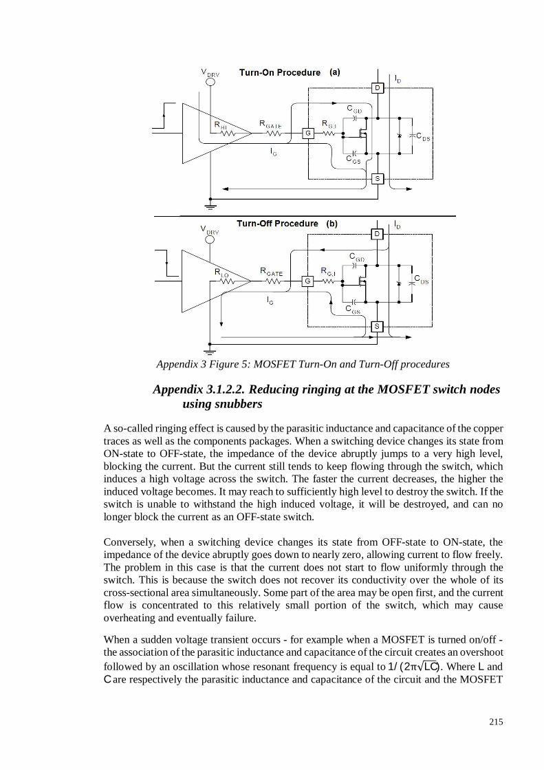
215
Appendix 3 Figure 5: MOSFET Turn-On and Turn-Off procedures
Appendix 3.1.2.2. Reducing ringing at the MOSFET switch nodes using snubbers
A so-called ringing effect is caused by the parasitic inductance and capacitance of the copper traces as well as the components packages. When a switching device changes its state from ON-state to OFF-state, the impedance of the device abruptly jumps to a very high level, blocking the current. But the current still tends to keep flowing through the switch, which induces a high voltage across the switch. The faster the current decreases, the higher the induced voltage becomes. It may reach to sufficiently high level to destroy the switch. If the switch is unable to withstand the high induced voltage, it will be destroyed, and can no longer block the current as an OFF-state switch. Conversely, when a switching device changes its state from OFF-state to ON-state, the impedance of the device abruptly goes down to nearly zero, allowing current to flow freely. The problem in this case is that the current does not start to flow uniformly through the switch. This is because the switch does not recover its conductivity over the whole of its cross-sectional area simultaneously. Some part of the area may be open first, and the current flow is concentrated to this relatively small portion of the switch, which may cause overheating and eventually failure.
When a sudden voltage transient occurs - for example when a MOSFET is turned on/off - the association of the parasitic inductance and capacitance of the circuit creates an overshoot followed by an oscillation whose resonant frequency is equal to 1/(2π√LC). Where L and C are respectively the parasitic inductance and capacitance of the circuit and the MOSFET

216
packages. This frequency is usually very high (around 200MHz) and creates disturbances which can damage nearby components.
To reduce the ringing a snubber circuitry can be implemented between the drain and the source of the MOSFET. This snubber circuit consists of a capacitor in series with a resistor which both need to be dimensioned precisely (Taylor and Manack, 2012). Snubbers are simple, efficient and cost effective open loop equalizers for SMPS. The purpose of a snubber is to control the balance between the rate of rise and the overshoots of transient switching in waveforms, in order to optimise the efficiency and reliability of a power supply. Snubbers can do many things:
Reduce or eliminate voltage or current spikes Limit dI/dt or dV/dt. Shape the load line to keep it within the safe operating area Transfer power dissipation from the switch to a resistor or a useful load. Reduce total losses due to switching Reduce EMI by damping voltage and current ringing
o Dimensioning the snubber capacitor:
To be able to dimension the capacitor properly, the ringing frequency (F1) must be determined by measuring the frequency of the signal at the switch node.
F1 = 1
2π√L1C1 (1)
To find L1 and C1, a capacitor C2 is added to the circuit and placed in parallel with C1 - between the drain and the source of the MOSFET. The value of C2 should be adjusted so that the ringing frequency F2 is half of F1:
F2 = 1
2 × F1 = 1
2π L1(C1 + C2) (2)
Since C2, F1and F2 are known, C1 can be calculated this way:
(1)
(2)
F1F2 =
C1 + C2C1
C1 = C2
F1F2 − 1
(3)
Solving C1 allows L1 to be calculated using equation (2). The value of the snubber capacitor must be at least 3 times higher than C1 (i.e. C ≥ 3C1).
o Dimensioning the snubber resistor:
The role of the snubber resistor is to dissipate the energy stored in the capacitor. The lower the resistor value, the better the damping of the ringing will be. However, the amount of energy to dissipate increases for lower resistor values, so the resistor wattage should be considered. The value of the resistor can be calculated with the following expression:
R = L1/C1 (4)

217
The power to dissipate is also depending on the switching frequency and the snubber capacitor value.
Appendix 3.1.3. Isolation between control and power parts
Most of the time - because of the power difference between those two parts – the control part is electrically isolated from the power part. This isolation is done by using optocouplers or magnetocouplers and protects the control part from any problem occurring in the power part.
On all the prototypes, the electrical isolation is guaranteed using an ADuM1100 100Mbps bus isolator from Analog Devices (Appendix 3 Figure 6). According to the datasheet, the ADuM1100 operates with a voltage supply ranging from 3.0 V to 5.5 V and boasts a propagation delay of <18 ns (Analog Devices, 2012). This component is perfectly suited for transmitting the high frequency control signals to the power part of the PSU.
Appendix 3 Figure 6: Functional block diagram of the magnetocoupler ADuM1100(Analog Devices, 2012)
Appendix 3.1.4. Current sensing for over-current protection
The resistive current sensing technique is the most commonly used technique for measuring electrical current on PCB assemblies at low or moderate current level. The amplifier best suited for this is the instrumentation amplifier.
In the drawing below (Appendix 3 Figure 7) the instrumentation amplifier amplifies the differential voltage (V ) to a usable level. To minimize voltage drop across the sense resistor, the resistor value is often sized to deliver a sense voltage of a few tens of millivolts at the maximum current level so as not to adversely affect I .or V .
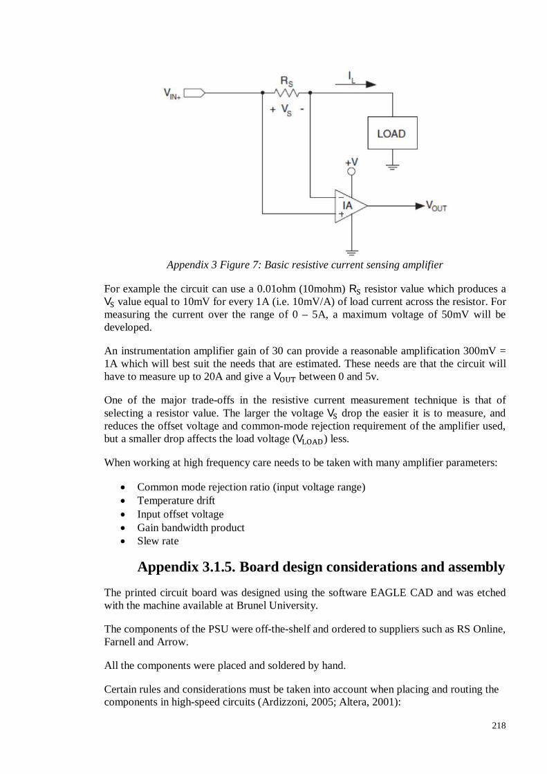
218
Appendix 3 Figure 7: Basic resistive current sensing amplifier
For example the circuit can use a 0.01ohm (10mohm) R resistor value which produces a V value equal to 10mV for every 1A (i.e. 10mV/A) of load current across the resistor. For measuring the current over the range of 0 – 5A, a maximum voltage of 50mV will be developed.
An instrumentation amplifier gain of 30 can provide a reasonable amplification 300mV = 1A which will best suit the needs that are estimated. These needs are that the circuit will have to measure up to 20A and give a V between 0 and 5v.
One of the major trade-offs in the resistive current measurement technique is that of selecting a resistor value. The larger the voltage V drop the easier it is to measure, and reduces the offset voltage and common-mode rejection requirement of the amplifier used, but a smaller drop affects the load voltage (V ) less.
When working at high frequency care needs to be taken with many amplifier parameters:
Common mode rejection ratio (input voltage range) Temperature drift Input offset voltage Gain bandwidth product Slew rate
Appendix 3.1.5. Board design considerations and assembly
The printed circuit board was designed using the software EAGLE CAD and was etched with the machine available at Brunel University.
The components of the PSU were off-the-shelf and ordered to suppliers such as RS Online, Farnell and Arrow.
All the components were placed and soldered by hand.
Certain rules and considerations must be taken into account when placing and routing the components in high-speed circuits (Ardizzoni, 2005; Altera, 2001):

219
The output of the driver must be as close as possible to the gate of the MOSFET, in order to minimize the inductance of the trace through which the high current is passing.
Whenever possible the low power components shall be grounded with a trace that is not common with the ground of the drivers. This mainly due to the fact that a high return current is flowing in the ground trace of the drivers, this creates noise and could make the low power components unstable.
Add bypass or decoupling capacitors for as many power supply traces as possible (Altera, 2001). The bypass capacitors shall be placed as close as possible to the power pins of the device in order to reduce the length of the high frequency current loop. This aspect is critical in high-speed board design.
All the unused input pins shall be tied to the ground whenever possible. The output pins shall be driven to a low state; this can be done by using pull down resistors connected to ground. A resistor value of 3600Ohms was used in the prototypes for this purpose.
Eliminate sockets whenever possible, sockets add parasitics. The number of outputs that can switch simultaneously shall be reduced and/or they
shall be spread across the board to make sure their influence is reduced. A ground plane shall be used whenever possible. The ground planes provides the
return current with a low-impedance path to ground, therefore reducing the influence of parasitic inductors and capacitors on the signal.
Power and ground pins shall be placed to each other, this reduces the overall inductance since the current from the supply pin (Vcc) flows in the opposite direction of the return current flowing in the ground (GND) pin.
Parasitics are hidden stray capacitors and inductors that must be considered when designing high-speed circuits (Appendix 3 Figure 8). They are created by the package leads and trace length, vias, pad to trace capacitors and many other elements in the circuit (Ardizzoni, 2005). Surface mount components shall be used to reduce the inductance of the leads and wide and short traces shall be used to connect vias to the devices (Altera, 2001).

220
Appendix 3 Figure 8: Typical op amp circuit, as designed (a) and with parasitics (b) (Ardizzoni, 2005)
‘Cross-talk is the unwanted coupling of signals between parallel traces’- (Altera, 2001). Signal coupling can result in unexpected component behaviour and a malfunctioning circuit. To reduce the influence of cross-talk on the traces, the center-to-center separation between the two traces should be at least 4 times the trace width (Altera, 2001).
All these considerations have been taken into account whenever possible. The use of 4-layer boards is optimum for reducing parasitics because it provides the possibility to have a power plane and two ground planes. Those planes can be used for stripline routing: surrounding the high-frequency trace in a ‘sandwich’ configuration as shown in Appendix 3 Figure 9.
Appendix 3 Figure 9: Illustration of stripline routing (Altera, 2001)
The fact that the prototypes were made on dual layer boards made it challenging to follow the routing guidelines and some trade-offs had to be made to make the assembly of the board feasible.

221
Appendix 4. DEVELOPMENT OF THE FIRST PULSE PSU PROTOTYPE
Appendix 4.1. First prototype: General presentation This first prototype demonstrated the critical influence of the inductance of the circuitry in high frequency applications. The successful design of the power supply unit not only resides in the choice of the components but also in the layout of the PCB. The schematic diagram of the first PSU prototype and its interface can be seen on the figure below:
Appendix 4 Figure 1: Schematic diagram of the first PSU prototype and its interfaces
Appendix 4.2. First prototype: The control circuitry The most critical component is the pulse generator; this device generates the logic signal that will actuate the MOSFETs on the power stage.
This control circuitry has been designed on a shield that is pin-to-pin compatible with the Max32 board so that it can be stacked on top of it. This modular approach makes the development on the prototypes easier, since each of the boards can be tested individually. Moreover, if a board fails to perform a function, a new board can be designed, without having to redesign and reassemble the other working parts.
Appendix 4.2.1. Pulsing circuitry for Pulse Width Modulated control
In the first prototype, the pulse generating function is performed by a MAX038. The MAX038 is a high-frequency precision function generator producing accurate waveforms at frequencies up to 20MHz such as:
triangle sine square
GND
VDC
Current sensing resistor
Control System
Workpiece
Tool
Over current protection
Peak detector
Magnetocoupler
Driver 1
Driver 2
Control circuitry
Magnetocoupler
Magnetocoupler
VDC
SW1
SW2
Signal conditioning

222
The type of waveform can be selected using inputs A0 and A1 with the combinations shown in the table below (Maxim, 2007):
Appendix 4 Figure 2: Waveform selection using inputs A0 and A1 (Maxim, 2007)
The frequency and the duty cycle can be adjusted independently using 3 inputs, allowing the generation of sawtooth and PWM signals. The inputs control the oscillator inside the MAX038, which is a relaxation type that operates by alternately charging and discharging the capacitor C connected to the COSC input:
IIN: Current input for frequency control which sets the nominal frequency of the output. IIN is used to control the charging and discharging current of the oscillator inside the MAX038. IIN can vary from 2µA to 750µA, producing more than two decades of frequency for any value of C .
DADJ: Duty-cycle adjust input. Applying ±2.3V to DADJ controls the duty cycle from 10% to 90%.
FADJ: Frequency adjust input. Applying ±2.4V to FADJ changes the nominal frequency (with VFADJ = 0V) by ±70%)
The frequency and the duty cycle of the output are controlled using an internal voltage reference (REF) of 2.5V. REF can furnish a stable current to IIN and can also be used to bias DADJ and FADJ.

223
Appendix 4 Figure 3: MAX038 pin
configuration (Maxim, 2007)
Appendix 4 Figure 4: Chart representing the output frequency as a function of IIN,
for different 퐶 values (Maxim, 2007)
The control circuitry of the first PSU prototype uses IIN and DADJ to vary the frequency and duty cycle of a square waveform. FADJ is disabled by being connected to ground though a 12kΩ resistance.
Appendix 4 Figure 5: Schematic diagram of the MAX038 signal generator
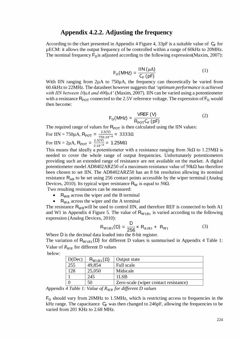
224
Appendix 4.2.2. Adjusting the frequency
According to the chart presented in Appendix 4 Figure 4, 33pF is a suitable value of C for µECM: it allows the output frequency of be controlled within a range of 60kHz to 20MHz. The nominal frequency F is adjusted according to the following expression(Maxim, 2007):
F (MHz) =IIN (μA)C (pF) (1)
With IIN ranging from 2µA to 750µA, the frequency can theoretically be varied from 60.6kHz to 22MHz. The datasheet however suggests that ‘optimum performance is achieved with IIN between 10μA and 400μA’ (Maxim, 2007). IIN can be varied using a potentiometer with a resistance R connected to the 2.5V reference voltage. The expression of F would then become:
F (MHz) =VREF (V)
R C (pF) (2)
The required range of values for R is then calculated using the IIN values: For IIN = 750µA, R = . ( )
.= 3333Ω
For IIN = 2µA, R = . ( ).
= 1.25MΩ This means that ideally a potentiometer with a resistance ranging from 3kΩ to 1.25MΩ is needed to cover the whole range of output frequencies. Unfortunately potentiometers providing such an extended range of resistance are not available on the market. A digital potentiometer model AD8402ARZ50 of a maximum resistance value of 50kΩ has therefore been chosen to set IIN. The AD8402ARZ50 has an 8 bit resolution allowing its nominal resistance R to be set using 256 contact points accessible by the wiper terminal (Analog Devices, 2010). Its typical wiper resistance R is equal to 50Ω. Two resulting resistances can be measured:
R across the wiper and the B terminal R across the wiper and the A terminal
The resistance R will be used to control IIN, and therefore REF is connected to both A1 and W1 in Appendix 4 Figure 5. The value of R is varied according to the following expression (Analog Devices, 2010):
R (D) =D
256 × R + R (3)
Where D is the decimal data loaded into the 8-bit register. The variation of R (D) for different D values is summarised in Appendix 4 Table 1: Value of 푅 for different D values below:
D(Dec) R (Ω) Output state 255 49,854 Full scale 128 25,050 Midscale 1 245 1LSB 0 50 Zero-scale (wiper contact resistance)
Appendix 4 Table 1: Value of 푅 for different D values
F should vary from 20MHz to 1.5MHz, which is restricting access to frequencies in the kHz range. The capacitance C was then changed to 246pF, allowing the frequencies to be varied from 201 KHz to 2.68 MHz.

225
The AD8402ARZ50 has a 3-wire SPI-compatible serial data input allowing the resistance R to be programmed.
Appendix 4.2.3. Adjusting the duty cycle
The value of V (in V) needed to produce a particular duty cycle can be calculated thanks to the formula(Maxim, 2007):
V (duty) =50
100− duty × 0.0575 (4)
Where duty is the value of the desired duty cycle in %. The second potentiometer is used the set the voltage V applied to DADJ. This time, the AD8402ARZ50 is wired as a potential divider with A2 connected to a voltage V = −2.5V and B2 connected to V = 2.5. Therefore a voltage V = V − V = −5V is applied to the potentiometer, as shown in Appendix 4 Figure 6. A general purpose dual operational amplifier LF353DRG4 is used to invert the voltage of the REF to produce the accurate -2.5V voltage connected to A2. W2 is connected to a second amplifier which is configured in a follower mode to provide a reliable voltage VDADJ. According to the datasheet of the AD8402ARZ50, the voltage V applied to the wiper can be calculated as follows (Analog Devices, 2010):
V (D) =D
256 × V + V (5)
The variation of V (V) for different D values is summarised in Appendix 4 Table 2: Value of 푉 for different D values Appendix 4 Table 2 below:
D(Dec) V (V) Output state 255 -2.48 Full scale 128 0 Midscale 1 +2.48 1LSB 0 +2.5 Zero-scale (wiper contact resistance)
Appendix 4 Table 2: Value of 푉 for different D values
Resistors R9 and R12 provide safety limits by preventing the voltage VDADJ to swing beyond +/- 2.31V.
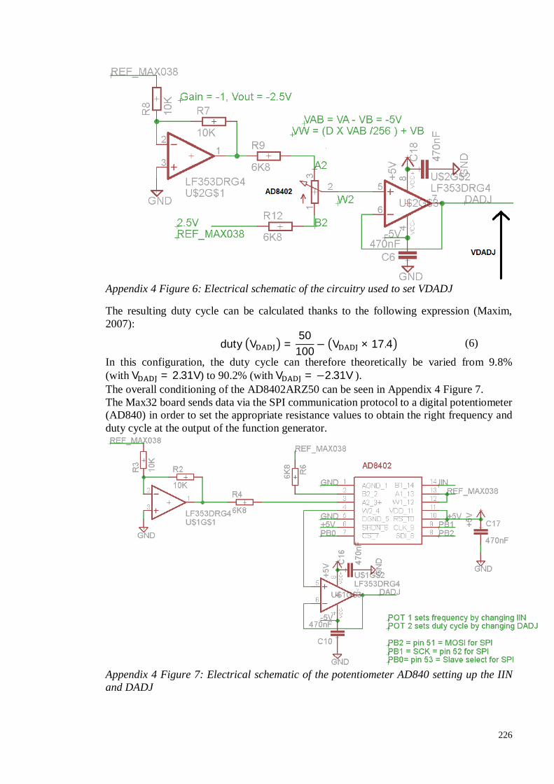
226
Appendix 4 Figure 6: Electrical schematic of the circuitry used to set VDADJ
The resulting duty cycle can be calculated thanks to the following expression (Maxim, 2007):
duty V =50
100− V × 17.4 (6)
In this configuration, the duty cycle can therefore theoretically be varied from 9.8% (with V = 2.31V) to 90.2% (with V = −2.31V ). The overall conditioning of the AD8402ARZ50 can be seen in Appendix 4 Figure 7. The Max32 board sends data via the SPI communication protocol to a digital potentiometer (AD840) in order to set the appropriate resistance values to obtain the right frequency and duty cycle at the output of the function generator.
Appendix 4 Figure 7: Electrical schematic of the potentiometer AD840 setting up the IIN and DADJ

227
Appendix 4.2.4. Conversion of the square wave signal to TTL signal
Since the output of the generator is a square wave, it needs to be converted to a 5V logic level signal. Two ultra-fast comparators (LT1719 from Linear Technologies) assure this task (Appendix 4 Figure 8), the first one compares the pulse voltage with the ground reference so its output goes to a 'High' state each the signal is positive. The other comparator is configured so that the output goes to a 'High' state each time the output of the function generator is negative, it is therefore the inverted signal from the other comparator. The first comparator will control the low side MOSFET of the half bridge and the second one will control the high side.
Appendix 4 Figure 8: Schematic diagram of the two ultrafast comparators LT1719 converting the MAX038 output signal to a 5V logic level
Appendix 4.2.5. Enabling and disabling the signals
The control signals are then sent to quad AND logic gate which allows the enabling/disabling of the control signals, the enabling/disabling function is simply done by changing the logic level a pin of the microcontroller from ‘Low’ to ‘High’.
The enabled signals are then sent to other AND gates but this time they are compared with the over current protection (OCP) logic signal. If the OCP signal is ‘High’, it means that it has not been triggered and the signals at the outputs of the AND gates can be sent to the MOSFETs.

228
If the over current protection is triggered, the OCP signal goes ‘Low’ which stops the sending of the control signal to the power stage and prevents the MOSFETs from being turned on when the output of the pulse power supply is short-circuited.
Therefore, the control signals are sent to the power stage only when the enable and OCP signals are both ‘High’ (Appendix 4 Figure 9).
Appendix 4 Figure 9: Electrical schematic of the control circuitry part
Appendix 4.2.6. Control Board power requirements and layout
The control board of the first prototype is bigger than the power and over current protection boards. This is mainly due to the fact that all the isolated power supplies for the power parts are soldered on this board to reduce the current path irregularities on the power and over-current protection boards. This board therefore contains the 12V isolated DC-DC converter supplying the high-side driver as well as the 12VDC to +/- 5V isolated converter supplying the over current protection board. Those converters can be seen on Appendix 4 Figure 10.
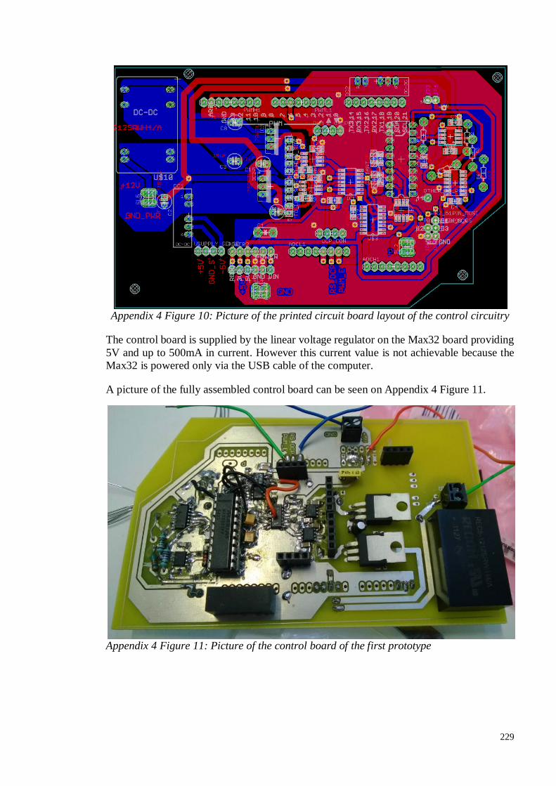
229
Appendix 4 Figure 10: Picture of the printed circuit board layout of the control circuitry
The control board is supplied by the linear voltage regulator on the Max32 board providing 5V and up to 500mA in current. However this current value is not achievable because the Max32 is powered only via the USB cable of the computer.
A picture of the fully assembled control board can be seen on Appendix 4 Figure 11.
Appendix 4 Figure 11: Picture of the control board of the first prototype

230
Appendix 4.3. First prototype: The power stage
Appendix 4 Figure 12: Simplified diagram of the power part connect to the interelectrode
gap
The power stage contains the MOSFET that will turn on/off to create the voltage pulses and can be represented by the simplified schematic below (Appendix 4 Figure 12).
Appendix 4.3.1. Timing aspects of the control signals
SW1 and SW2 are controlled according to the signals showed in Appendix 4 Figure 13.
When SW2 is turned ON and SW1 is turned OFF (situation number 1), the voltage VDC is applied to the IEG and machining occurs: this is the pulse on-time.
When SW1 is turned ON and SW2 is turned OFF (situation number 3), the IEG gap is in short circuit situation: this is the pulse off-time.

231
Appendix 4 Figure 13: Diagram representing the timing of the 2 signals controlling the MOSFETs SW1 and SW2
It is very important that SW1 and SW2 are not turned ON at the same time, which would short circuit the power supply VDC. For this reason, a dead-time generating circuit (Appendix 4 Figure 14) must control the dead-time between the ON and OFF signals actuating SW1 and SW2 (2).
The dead time circuitry ensures there is no cross-conduction of the MOSFETs which would short-circuit the output of the power supply. It is made of an AND logic gate, a resistor, a diode and a capacitor. The aim of the resistor-capacitor (RC) network is to delay the signal before it arrives at the input B, so that the output Y stays low during this time. The duration of the dead time is set to match the turn-on and turn-off times of the MOSFET in order to avoid having two conducting MOSFETs at the same time. According to the datasheet of the FDMS7578 (Fairchild-Semiconductor, 2009), the typical turn-on delay time is 8ns, whereas the typical turn-off delay time is 20ns. This means that there is a possibility for both MOSFETs to conduct at the same time for 12ns, which can damage the PSU at high switching frequencies.
The AND logic gate is a 74V1G08 from STMicroelectronics which has a ‘High Level Input Voltage’ of 0.7 × Vcc (STMicroelectronics, 2004). Since the 74V1G08 has a 3.3V supply, the input is detected as ‘HIGH’ when it reaches 2.31V. The RC time constant of the RC network constant is defined as the time it takes for the voltage across the capacitor to reach 63% of its maximum value. Since the logic voltage on the board is 3.3V, with a capacitor value of 33pF and a resistor of 360Ω the voltage at the input B should theoretically reach 2.08V in 11.88 ns (i. e. 360 × 33 × 10 = 11.88 × 10 ).
This delay should therefore ensure a reliable operation of the pulse PSU.

232
Appendix 4 Figure 14: Schematic diagram of the dead-time circuitry of the first prototype
The role of the diode is to provide a quick discharge path for the current in the capacitor in order to have a quick signal transition from the HIGH to the LOW state. This prevents the turn-off command from being delayed by the RC network.
Appendix 4.3.2. MOSFET selection
The MOSFETs have been selected to the following criteria:
Operating voltage Operating current Turn-on and turn off-time Package shall allow soldering by hand
The selected MOSFET is a FDMS7578 from Fairchild Semiconductors (Appendix 4 Figure 15). This N-Channel MOSFET has been designed specifically to improve the overall efficiency and to minimize switch node ringing of DC/DC converters using either synchronous or conventional switching PWM controllers. It has been optimized for low gate charge, low ON resistance (R ( )), fast switching speed and body diode reverse recovery performance (Fairchild-Semiconductor, 2009).

233
Appendix 4 Figure 15: CAD Model of the package (Power 56) and representation of the MOSFET FDMS7578 (Fairchild-Semiconductor, 2009)
The main characteristics of the FDMS7578 are summarised below (Appendix 4 Table 3):
Parameters Value Unit Maximum drain to source voltage V 25 V
Maximum drain current I 17 continuous 60 pulsed A
Drain-source on resistance, R ( ): 0.0058 Ω Typical Turn-On Delay time 8 ns Typical Rise Time 2.6 ns Typical Turn-Off Delay time 20 ns Typical Fall Time 2.2 ns Maximum Gate-source voltage, V : +/-20 V Gate-source threshold voltage V : 1.6 V Source ohmic resistance: 0.0025 Ω Drain ohmic resistance: 0.0025 Ω Input capacitance C : 1221 pF Reverse transfer capacitance C : 54 pF
Appendix 4 Table 3: Table summarizing the main characteristics of the MOSFET FDMS7578
Appendix 4.3.3. Driver selection
The UCC27201DG4 high frequency N-Channel MOSFET driver includes a high-side/low-side driver with independent inputs for maximum control flexibility. This allows for N-Channel MOSFET control in half-bridge or full-bridge converters. The low-side and the high-side gate drivers are independently controlled and matched to 1-ns between the turn-on and turn-off of each other (TI, 2008).
In most cases, controlling the high-side MOSFET requires the use of a bootstrap diode and a bootstrap capacitor to create a floating reference at its source - allowing a gate-source voltage V to be applied. However the desired switching frequency of the pulse power supply is too high to use such configuration. The high-side gate driver is therefore not used and each MOSFET will have its own driver. A floating ground (GND_FLOAT) is provided to the high-side driver using an isolated 12V DC-DC converter (Appendix 4 Figure 16).
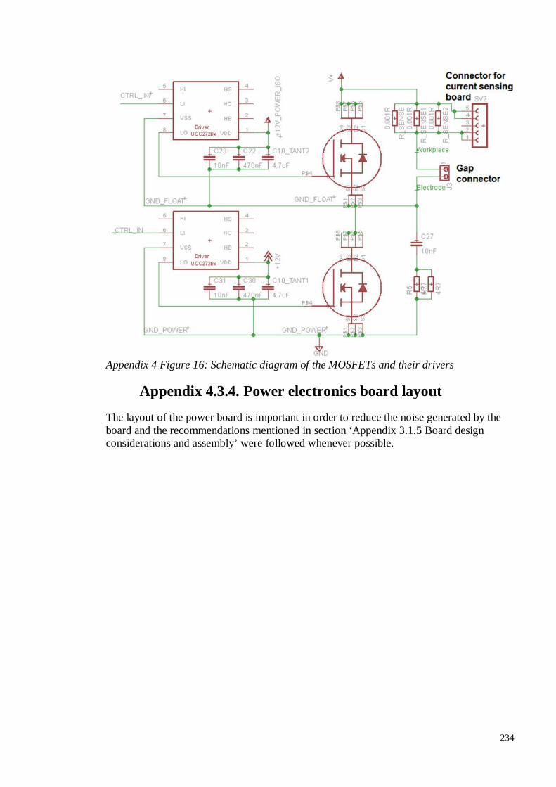
234
Appendix 4 Figure 16: Schematic diagram of the MOSFETs and their drivers
Appendix 4.3.4. Power electronics board layout
The layout of the power board is important in order to reduce the noise generated by the board and the recommendations mentioned in section ‘Appendix 3.1.5 Board design considerations and assembly’ were followed whenever possible.

235
Appendix 4 Figure 17: Picture of the printed circuit board layout of the control circuitry
A picture of the fully assembled power board can be seen on Appendix 4 Figure 18.
Appendix 4 Figure 18: Picture of the power board of the first prototype
Dead-time circuitry
Drivers MOSFETs Current sensing
resistors

236
Appendix 4.4. First prototype: The current sensing board
The current flowing through the IEG is measured via a sensing resistor in series with the gap. The voltage across this resistor is amplified and sent to both the over current protection (for power supply safety purposes) and the control system –via a peak detector– (for gap control purposes).
According to Ohm’s law, the voltage across this resistor is an image of the current flowing through the system. This voltage is measured using a current feedback amplifier EL5166ISZ which has a very high bandwidth of 1.4GHz and a 6000V/µs slew rate (Intersil, 2010). It is therefore suitable for the detection and amplification of small high frequency signals similar to the signal across the current sensing resistor.
The output of the differential amplifier goes to 2 different parts: 1) the over current protection (OCP) and 2) the peak detector.
Appendix 4 Figure 19: Electrical schematic of the current sensing circuitry featuring the amplifier EL5166ISZ
The current sensing resistor has value of 25mΩ, which means that a measured voltage of 25mV corresponds to 1A. The differential amplifier has a gain of 13.75 and is set using the equation:
G = RF1/RG1 = RF2/RG2 (7) The on-board current scale is therefore 0.025 × 13.75 = 0.344 V/A.
Due to the low precision of the resistors setting the gain, the actual scale is 0.385V/A.
Appendix 4.4.1. Over current protection (OCP)
The OCP circuitry (Appendix 4 Figure 20) is made of a comparator which will compare the output of the differential amplifier with the OCP level set by the microcontroller. The

237
comparator used for this application is very fast: it is a LT1719 from linear technology and features a very short 4.5ns propagation delay.
The OCP threshold level is set by filtering one of the PWM outputs of the microcontroller with an RC filter. If the measured current is higher than the defined threshold level, the output of the comparator will go HIGH. The signal is its HIGH state will then go through a magnetocoupler (which ensures the isolation between the OCP circuitry and the control circuitry) and will then set the S/R latch gate to HIGH as well. The S/R latch gate will remain in a latched state until it is reset by the Max32 microcontroller board sending a 1ms pulse to the RES_R pin.
The OCP signal connected to the AND gates in the previously seen control circuitry actually corresponds to the OCP_LATCH/ signal, as the signal needs to go LOW to stop the PSU from pulsing. On the other end, the OCP_LATCH signal is connected to a red LED (not presented in the schematic) which will light up to signal to the operator that the PSU has been stopped because of an OCP event.
Appendix 4 Figure 20: Schematic of the OCP circuitry
Appendix 4.4.2. The peak detector
The peak detector plays a very important role as it delivers the peak value of the current to the motion controller. It is used to control the interelectrode gap as an input variable for the control algorithm. This peak detector circuitry uses a transistor (Q1) instead of a diode in order to reduce the rise time of the pulse (Appendix 4 Figure 21). When a pulse is detected, the operational amplifier LM7171 will charge the capacitor CDECAY via the resistor R_RISE – which sets the charging time of CDECAY. During the pulse off time the voltage across CDECAY decreases slowly as this latter is discharging itself through the resistor R_DECAY. The role of the transistor is to control the discharging current of CDECAY.

238
Appendix 4 Figure 21: Peak detector circuitry
Appendix 4.4.3. First prototype: firmware programming
The firmware of the PSU has been programmed using the MPIDE developing environment. This programme allows you to write a programme, compile it and the download it to the Max32 development board via an USB cable. The programme will start executing as soon as the Max32 is powered up, allowing it to run in standalone mode and its execution workflow is summarised in Appendix 4 Figure 22.
If no data is received, the programme stays in ‘idle’ mode and disables the pulses if the OCP is triggered.
The programme starts a sequence of instructions as soon as it receives data. The data is extracted from a character buffer and each parameter is converted from a string to a long integer using the standard atol() C function.
When all the data is received, the OCP is reset by the microcontroller which send a 50ms pulse to the reset pin of the S/R latch.
The controller then starts calculating the value of IIN using the formula:
IIN (μA) =C (pF) × F (Hz)
1000000 (8)
Then the controller checks if the condition 2μ퐴 < 퐼퐼푁 < 750μ퐴 is satisfied, if that is not the case it aborts and returns to its ‘idle’ mode.

239
Appendix 4 Figure 22: Flowchart describing the firmware workflow running on the first PSU prototype
If IIN has a correct value, the resistance R is calculated. R corresponds to R , the resistance of the potentiometer AD8402 connecting REF to IIN.
R = R =REFIIN (9)
R is then used to calculate the value of levelRfreq which is the decimal value ranging from 0 to 255 needed to programme the AD8402:
levelRfreq = 푟표푢푛푑R − R × 256
R (10)
The value of levelRfreq is then assessed to prevent the digital potentiometer from being configured with wrong values:
If levelRfreq > 255, then levelRfreq is set to 255 If levelRfreq < 0, then levelRfreq is set to 0
The value of levelRfreq is then to the digital potentiometer using the SPI communication protocol. The programme uses the standard SPI library provided by mpide. The function of

240
the SPI library were wrapped in the function digitalPotWrite() presented in Appendix 4 Figure 23.
Appendix 4 Figure 23: the digitalPotWrite() function used to communicate with the AD8402 digital potentiometer
The same approach was used for setting up the duty cycle:
1- The value of the duty cycle is checked and readjusted if necessary 2- The voltage VDADJ needed to reach the desired duty cycle is calculated 3- The resistance R value of the potentiometer needed to adjust VDADJ is
calculated 4- The decimal value levelDuty (0-255) is calculated using the value of R and
readjusted if it is out of the 0 and 255 boundaries 5- The decimal value levelDuty is sent to the digital potentiometer using the function
digitalPotWrite()
Once both potentiometers have been configured, the controller will set the OCP trigger threshold by using one of its pulse width modulated (PWM) outputs. Pin 5 outputs the PWM signal with a frequency of 500Hz and is connected to the input of a ADUM1100 magnetocoupler. The output of the magnetocoupler is connected to a low-pass filter (on the OCP board) which is itself connected to the – input of the ultrafast LT1719 comparator.
The function SoftPWMServoPWMWrite() controls the PWM signal and is a standard function of the SoftPWMServo library.
Finally, after the OCP threshold is setup, the pulses are enabled. This operation is done by setting the pin A6 to a HIGH state which satisfying the AND condition of the AND gate on the circuit board.
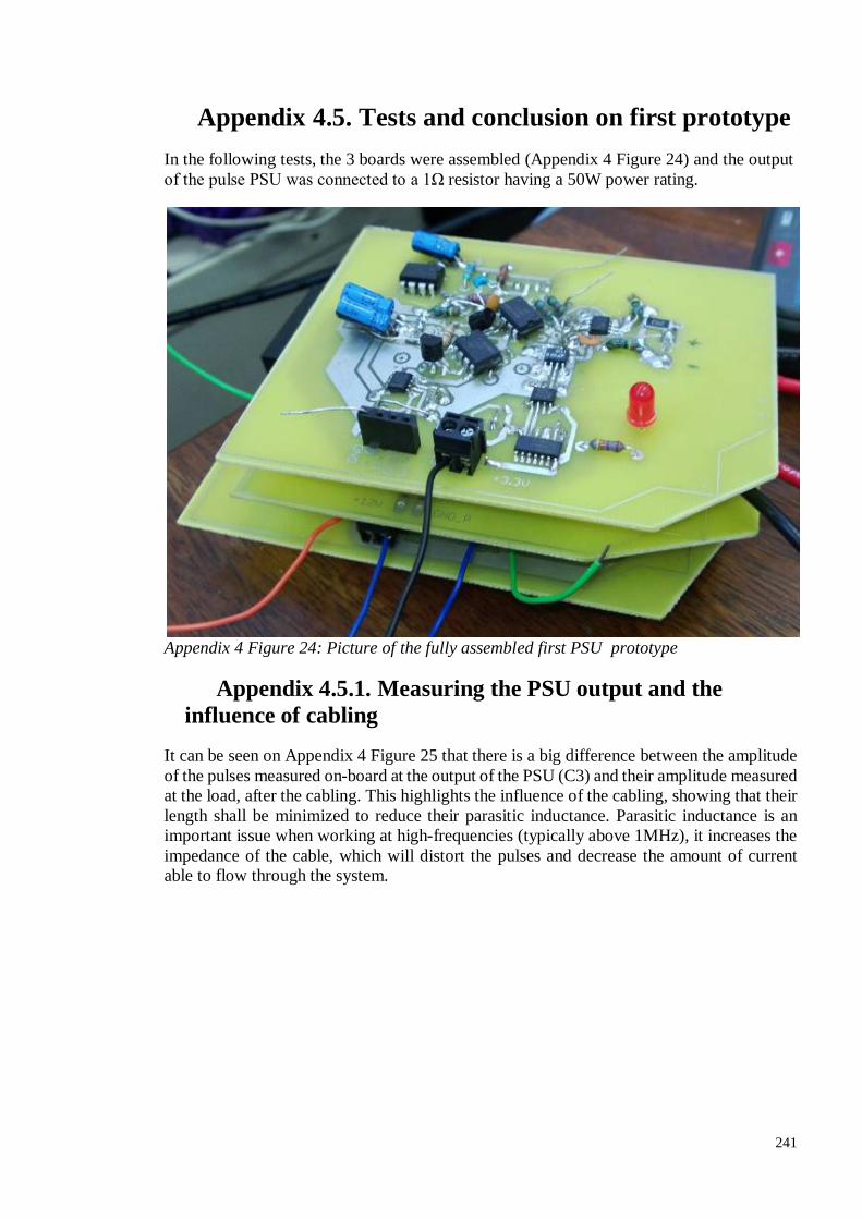
241
Appendix 4.5. Tests and conclusion on first prototype In the following tests, the 3 boards were assembled (Appendix 4 Figure 24) and the output of the pulse PSU was connected to a 1Ω resistor having a 50W power rating.
Appendix 4 Figure 24: Picture of the fully assembled first PSU prototype
Appendix 4.5.1. Measuring the PSU output and the influence of cabling
It can be seen on Appendix 4 Figure 25 that there is a big difference between the amplitude of the pulses measured on-board at the output of the PSU (C3) and their amplitude measured at the load, after the cabling. This highlights the influence of the cabling, showing that their length shall be minimized to reduce their parasitic inductance. Parasitic inductance is an important issue when working at high-frequencies (typically above 1MHz), it increases the impedance of the cable, which will distort the pulses and decrease the amount of current able to flow through the system.

242
The frequency was set to 2.5MHz and the duty cycle was 20%. The pulse voltage was adjusted manually to 6V.
Appendix 4 Figure 25: C1 (yellow): current measured from external current sensor (1V/div.,1V/A); C2 (pink): voltage measured across the load, after the cables (2V/div.); C3 (cyan): voltage measured at the output of the pulse PSU, on the board connectors (2V/div.). Frequency: 2.5MHz duty cycle: 20%.
The frequency was then lowered to 800kHz and the voltage was set to 5V to prevent the load from heating up too much. It can be seen on Appendix 4 Figure 26 that the voltage at the load is much higher than when it was at 2.5MHz. Moreover, the amplitude of the current pulses is much high also, reaching 2.5A. This confirms the necessity for a low impedance cables to be used in µECM.

243
Appendix 4 Figure 26: C1 (yellow): current measured from external current sensor (1V/div.,1V/A); C2 (pink): voltage measured across the load, after the cables (2V/div.); C3 (cyan): voltage measured at the output of the pulse PSU, on the board connectors (2V/div.). Frequency: 800kHz duty cycle: 20%.
Appendix 4.5.2. On-board signal measurement
Appendix 4 Figure 27: Signals on the current sensing board

244
Channel Description Scaling C1 Measured gap current via
commercial current sensor 1V/div., 1V/A
C2 Measured gap current via on-board current sensing circuitry
380mV/div., 380mV/A
C3 OCP threshold level 380mV/div., 380mV/A C4 Measured voltage across the
resistance (inverted to avoid short circuits)
380mV/div., 380mV/A
Appendix 4 Table 4: Description of the signals measured in Appendix 4 Figure 27
On Appendix 4 Figure 27 it can be seen that the shape of the current measured with the on-board circuitry (C2) is very similar to the one measured with the commercially available current sensor (C1). The peak detector is working as expected and its output signal can be seen in channel C3. However, the presence of noise on channel C2 and C3 can be observed. This noise is generated when the MOSFETs are switched ON and OFF.
Appendix 4.5.3. Conclusions regarding the first PSU prototype
The first prototype delivered the expected results despite off the noise present in the sensing circuitry. However, some limitations have been observed:
The way the MAX038 function generator is configured prevents a wide range of frequency to be reached because the C capacitance used to the oscillator cannot be changed automatically.
There is no possibility to reverse to polarity is a programmed way. The only way to do so is to swap the cable connections.
It is not possible to apply a negative or positive voltage offset voltage during the pulse of time
The size of the board is too big and the footprint of the board shall be optimized.
This prototype was mainly considered as a proof of concept to validate the choice for the core components and the 3-board modular architecture. It has been deduced that this concept would be a viable way to develop the other prototypes.

245
Appendix 5. PULSE PSU SIMULATION WITH MATLAB/SIMULINK
Appendix 5.1. Basic model (ideal) To simulate the behaviour of the pulse PSU prototype, a model of the circuitry has been realised using MATLAB/Simulink.
The MOSFET switches used in the pulse PSU design are FDMS7578 N-channel MOSFETs from Fairchild Semiconductor. They have been chosen because of their very fast turn-on and turn-off times (respectively 8 and 20ns).
The behaviour of the MOSFET is simulated by the Simulink library component ‘N-Channel MOSFET’ and its parameters (Appendix 5 Table 1) have been set according to the values available in the datasheet of the FDMS7578 (Fairchild-Semiconductor, 2009).
Parameters Value Unit Drain-source on resistance, R_DS(on): 0.0058 Ω Drain current, Ids, for R_DS(on): 17 A Gate-source voltage, Vgs, for R_DS(on): 10 V Gate-source threshold voltage Vth: 1.6 V Source ohmic resistance: 0.0025 Ω Drain ohmic resistance: 0.0025 Ω Input capacitance Ciss: 1221 pF Reverse transfer capacitance Crss: 54 pF
Appendix 5 Table 1: Table summarizing the parameters of the N-Channel MOSFET Simulink component used in the simulation
The pulse PSU model used in the simulation is represented in Appendix 5 Figure 1:
Appendix 5 Figure 1: Model of the second prototype of the pulse PSU

246
The value of the DC voltage source for pulses was set to 6V, whereas the DC source for the offset was set to 2V. The load is represented by a resistor of 1Ω.
Appendix 5 Figure 2: Simulation result: evolution of the IEG voltage (V) over time (s) in steady state
Diode forward voltage has been set to 1V, therefore the negative Offset during the pulse off-time is closer to -1V instead of -2V (which is the value of the source).
Appendix 5.2. Realistic model (including parasitics) The following model has been modified by adding parasitic inductance and snubber capacitors. Cables have a parasitic inductance of 75nH and to model its influence on the pulses, inductors have been added to the circuit.
It can be observed that the inductance of the cables decreases the rise time of the pulses and will therefore be an issue when sending high frequency pulses to the IEG. On the other hand, a negative kick can be observed after each pulse. Changing the values of the snubber resistors and capacitors affects the shape of this negative transient signal. Conclusions for second PSU prototype

247
Appendix 5 Figure 3: Electrical schematic diagram of the power stage used in the Simulink simulation
Appendix 5 Figure 4: Simulation result: evolution of the IEG voltage (V) over time (s) in steady state when the parasitics have been added

248
Appendix 6. SECOND PULSE PSU PROTOTYPE The second PSU was designed according to the simulation results from the previous appendix.
Appendix 6.1. Second PSU prototype: control circuitry
Appendix 6.1.1. Pulse generating module This module generates the signal controlling the MOSFETs. The frequency needs to be variable over a range, 1 kHz to 5MHz, with a duty cycle changing from 5% to 100% (DC).
The solution adopted is shown in Error! Reference source not found. and uses two components: an oscillator and a pulse generator.
Appendix 6 Figure 1: Electrical schematic diagram of the oscillator and the pulse generator
Oscillator
The LTC6904 is a low power self-contained digital frequency source providing a precision frequency from set through a serial port. This programmable oscillator is capable of generating a 5V logic signal at a frequency varying from 1kHz to 68MHz. The LTC6904 requires no external components other than a power supply bypass capacitor, and it operates over a single wide supply range of 2.7V to 5.5V.
The frequency of the oscillator is set according to the following equation (Linear Technology, 2014):
f = 2 .2078(Hz)
(2− DAC1024)
(1)
OCT is a four-bit digital code and DAC is a ten-bit digital code. Evaluating this formula to calculate OCT and DAC from a required frequency f, gives the following statements:

249
OCT = 3.22logf
1039 ,
DAC = round 2048−2078(Hz). 2( )
f (2)
The output of the programmable oscillator LTC6904 is connected to the trigger input of the programmable pulse generator 3D7622-0.25 (Error! Reference source not found.Figure 4-2). The pulse generator will therefore output pulses at each rising edge of the signal coming from the LTC6904, thus creating a pulse train with adjustable frequency and duty cycle.
Modulation component
The Data Delay Devices 3D7622-0.25 device is a twenty two bit serial programmable pulse generator that operates with either CMOS or TTL logic levels (Data Delay Devices, 2008).
A rising edge on the trigger input (TRIG) initiates a pulse, which is presented on the output pins (OUT, OUTB) and ends at a time determined by the address loaded into the device via SPI serial interface. The pulse width, programmed via the serial interface, can be varied over 4,194,303 equal steps of 0.25ns. The 3D7622-0.25 has a minimum pulse width of 14.0ns and a maximum pulse width of 1.05ms. The pulse width can be varied according to the formula (Data Delay Devices, 2008):
t = t + addr + t (3)
Where addr is the programmed address, t is the pulse width increment (equal to 0.25ns) and t inherent pulse width (equal to 14ns). The device also offers a reset input (RES) to terminate the pulse before the programmed pulse duration has expired.
The Arduino compatible Max32 development board is directly interfaced with the human machine interface (HMI), which sends all the data necessary to configure the pulse PSU: frequency, duty cycle, over current protection threshold and desired pulse shape. The microcontroller then sets the frequency by communicating with the programmable oscillator via I2C and also sets the duty cycle thanks to the pulse generator using the SPI communication protocol.
Appendix 6.1.2. Pulse shape selection
A multiplexer defines the polarity of the pulsed voltage. Signals PWM and PWM/ correspond respectively to outputs OUT and OUTB of the pulse generator. OUT and OUTB generate signals that are logically inverted from each other: if OUT is HIGH (5V) then OUTB is LOW (0V) and vice versa.

250
Appendix 6 Figure 2: Control circuitry of the second PSU prototype
If PIN8 is LOW (0V), Channel A is selected, so SW1 and SW4 are synchronized with SW_pulse whereas SW2 and SW3 are synchronized with SW_offtime. This results in the following configuration (Appendix 6 Figure 3):
Appendix 6 Figure 3: Drawing representing the 4 different control signal used to change the pulse shape when Channel A is selected.
If PIN8 is HIGH (5V), Channel B is selected, so SW2 and SW3 are synchronized with SW_pulse whereas SW1 and SW4 are synchronized with SW_offtime. The following signals are obtained (Appendix 6 Figure 4):
Control signal for SW1 and SW4
Control signal for SW2 and SW3
Control signal for the Pulse switch
Control signal for the Offset switch
PIN8 (selects the logic of channel 1 & 2)
Signals coming from the pulse generator (pins OUT and OUTB)

251
Appendix 6 Figure 4: Drawing representing the 4 different control signal used to change the pulse shape when Channel B is selected
The following drawing (Appendix 6 Figure 5) describes the different pulse shapes that can be obtained with the developed power supply:
Control signal for SW1 and SW4
Control signal for SW2 and SW3
Control signal for the Pulse switch
Control signal for the Offset switch

252
Appendix 6 Figure 5: Drawing of the different pulse shapes that can be obtained in the different configuration
Appendix 6.1.3. Avoiding MOSFET cross conduction
Appendix 6 Figure 6: Electrical schematic of the dead time circuitry used in the PSU
The dead time circuitry ensures there is no cross-conduction of the MOSFETs which would short-circuit the output of the power supply. It is made of an AND logic gate, a resistor, a diode and a capacitor (Appendix 6 Figure 6). The aim of the resistor-capacitor (RC) network is to delay the signal before it arrives at the input B, so that the output Y stays low during this time. The duration of the dead time is set to match the turn-on and turn-off times of the MOSFET in order to avoid having two conducting MOSFETs on the same side of the H Bridge (which would create a short circuit situation). According to the datasheet of the FDMS7578 (Fairchild-Semiconductor, 2009), the typical turn-on delay time is 8ns, whereas

253
the typical turn-off delay time is 20ns. This means that there is a possibility for both MOSFETs to conduct at the same time for 12ns, which can damage the PSU at high switching frequencies.
To reduce the noise generated by the MOSFETs during their turn-on and turn-off transitions, a resistor of 4.7Ω is added in series between the output of the MOSFET driver and the gate of the MOSFET. The aim of this resistor is to reduce the value of di/dt by increasing the charging time of the input capacitance C of the MOSFET. The datasheet mentions typical values of C = 1221pF for the gate capacitance and an internal gate resistance of 1.2Ω. Adding an external gate resistor of 4.7 therefore sets the charging of the gate capacitor to 7.2ns ((4.7 + 1.2) × 1221. 10 = 7.2 × 10 ).
The AND logic gate is a 74V1G08 from STMicroelectronics which has a ‘High Level Input Voltage’ of 0.7 × Vcc (STMicroelectronics, 2004). Since the 74V1G08 has a 3.3V supply, the input is detected as ‘HIGH’ when it reaches 2.31V. The RC time constant (τ = RC) of the RC network constant is defined as the time it takes for the voltage across the capacitor to reach 63% of its maximum value. Since the logic voltage on the board is 3.3V, with a capacitor value of 33pF and a resistor of 360Ω the voltage at the input B should theoretically reach 2.08V in 11.88 ns (360 × 33 × 10 = 11.88 × 10 ).
This delay should therefore ensure a reliable operation of the pulse PSU.
The role of the diode is to provide a quick discharge path for the current in the capacitor in order to have a quick signal transition from the HIGH to the LOW state. This prevents the turn-off command from being delayed by the RC network.
Appendix 6 Figure 7: Measurement of the dead time between the control signals to the 2 low side switches of the H-bridge; frequency: 5MHz, duty cycle: 25%
Appendix 6.2. Second PSU prototype: power stage Different voltages can be applied to the H-bridge thanks to two MOSFETs, allowing to apply a lower voltage during the pulse off-time. A Schottky barrier prevents current from

254
flowing from V_PULSE to V_OFFSET (because V_PULSE is greater than V_OFFSET and the MOSFETs have built-in parallel diodes).
Appendix 6 Figure 8: Schematic of the MOSFETs switching between the PULSE and OFFSET voltages to be applied to the H-bridge
The drivers of the MOSFETs SW_pulse, SW_offset, SW1 and SW3 are isolated from the ground thanks to 4 individual isolated DC-DC converters. This allows driving the MOSFETs at a very wide range of frequencies and duty cycles.
To optimise the layout of the power stages, it has been decided that the drivers would be powered by the control circuitry board. The isolated DC-DC converters are therefore not present on the power stage, but on the control stage.
A pin connector placed close to the current sensing resistors allows the current sensing circuitry board to be plugged onto the power stage. The output of the current sensing circuitry board is interfaced with the control stage in order to interrupt the pulsing when the over current protection is triggered.

255
Appendix 6 Figure 9: Schematic of the MOSFETs in the H-bridge
Configuration of the snubbers
Each of the switches on the power board has its own snubber circuitry which is made of a 10nF capacitor in series with two 500mW 10Ω resistors in parallel (equivalent resistance 5Ω). The snubbers damp the ringing which occurs when the switches are turned ON or OFF.
The following figures illustrate the improvement in pulse shape when the snubber circuitry is mounted of the power stage: it can be seen that the ringing is significantly reduced thanks to the snubbers, resulting in a better pulse shape.

256
Appendix 6 Figure 10: Output of the second PSU prototype without any snubber circuitry, in mode 3, 3V pulse and 1V negative offset, 2MHz with 25% Duty cycle, no load.
Appendix 6 Figure 11: Output of the second PSU prototype with snubber circuitry in mode
3, 3V pulse and 1V negative offset, 2MHz with 25% Duty cycle, no load.
Some heat sinks have been placed on the MOSFETs and their drivers to help them cool down when the pulse PSU is switching at high frequencies.
Testing of the PSU output
In this section, the output of the PSU is connected to a 1Ω 50W resistor which simulates the gap and allows high current to flow through the PSU (as shown on the figure below).

257
Commands are then sent to the PSU via the developed HMI and the obtained pulse shapes are visualized with a scope. The current flowing though the resistor is measured thanks to a current transformer.
Appendix 6 Figure 12: Picture of the second PSU prototype being tested with a 1Ω load.
Appendix 6 Figure 13: C1: current (1V/A), C2: voltage; PSU in pulse mode 1: 3V pulse,
no offset; 750kHz 25% duty cycle

258
Appendix 6 Figure 14: C2: voltage; PSU in pulse mode 2: 2VDC (positive)
Appendix 6 Figure 15: C1: current (1V/A), C2: voltage; PSU in pulse mode 3: 3V pulse, 1
V negative offset; 750kHz 25% duty cycle

259
Appendix 6 Figure 16: C1: current (1V/A), C2: voltage; PSU in pulse mode 4: 3V pulse, 1
V positive offset; 750kHz 25% duty cycle
Appendix 6 Figure 17: C1: current (1V/A), C2: voltage; PSU in pulse mode 5: 3V
negative pulse, no offset; 750kHz 25% duty cycle

260
Appendix 6 Figure 18: C2: voltage; PSU in pulse mode 6: 2VDC (negative)
Appendix 6 Figure 19: C1 current (1V/A), C2: voltage; PSU in pulse mode 7: negative 3V
pulse, 1 V positive offset; 750kHz 25% duty cycle
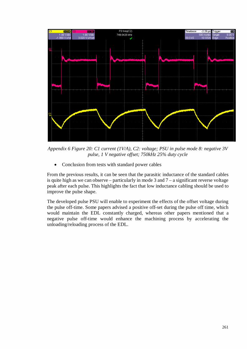
261
Appendix 6 Figure 20: C1 current (1V/A), C2: voltage; PSU in pulse mode 8: negative 3V pulse, 1 V negative offset; 750kHz 25% duty cycle
Conclusion from tests with standard power cables
From the previous results, it can be seen that the parasitic inductance of the standard cables is quite high as we can observe – particularly in mode 3 and 7 – a significant reverse voltage peak after each pulse. This highlights the fact that low inductance cabling should be used to improve the pulse shape.
The developed pulse PSU will enable to experiment the effects of the offset voltage during the pulse off-time. Some papers advised a positive off-set during the pulse off time, which would maintain the EDL constantly charged, whereas other papers mentioned that a negative pulse off-time would enhance the machining process by accelerating the unloading/reloading process of the EDL.

262
Appendix 6.3. Second PSU prototype: over current protection (OCP) stage
The over current protection (Appendix 6 Figure 21) on the second prototype is similar to the one on the first prototype: the current is measured via a sensing resistor and sent to a comparator as well as a peak detector. The comparator compares the measured current with a threshold set by the microcontroller. On the other hand, the peak detector provides the control system with a reliable current value.
Appendix 6 Figure 21: Electrical diagram of the current sensing part on the OCP stage of the second prototype
Testing of the OCP stage The OCP stage is mounted on the top of the power stage, as shown on the picture below. The output of the PSU is connected to a 1Ω load.
Appendix 6 Figure 22: Picture of the OCP stage being tested and refined.
On Appendix 6 Figure 23, the OCP can be seen triggering when the current goes above 3A. The comparator output goes HIGH for a very short amount of time, but this time is sufficient to make the SR flip-flop latch and stop the pulses.

263
Appendix 6 Figure 23: C1: OCP threshold (380mV/A); C2: comparator output; C3: OCP
signal (latched output); C4: current (380mV/A); 1MHz 25% duty cycle
Appendix 6 Figure 24: C1: OCP threshold (380mV/A); C2: comparator output; C3: OCP
signal (latched output); C4: current (380mV/A); 1MHz 25% duty cycle (20ns/div)
From a timing perspective, the pulses are stopped approximately 40ns after the comparator triggers the over current protection signal (Appendix 6 Figure 24).
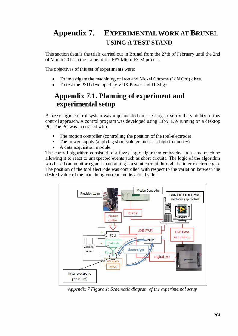
264
Appendix 7. EXPERIMENTAL WORK AT BRUNEL USING A TEST STAND
This section details the trials carried out in Brunel from the 27th of February until the 2nd of March 2012 in the frame of the FP7 Micro-ECM project.
The objectives of this set of experiments were:
To investigate the machining of Iron and Nickel Chrome (18NiCr6) discs. To test the PSU developed by VOX Power and IT Sligo
Appendix 7.1. Planning of experiment and experimental setup
A fuzzy logic control system was implemented on a test rig to verify the viability of this control approach. A control program was developed using LabVIEW running on a desktop PC. The PC was interfaced with:
• The motion controller (controlling the position of the tool-electrode) • The power supply (applying short voltage pulses at high frequency) • A data acquisition module
The control algorithm consisted of a fuzzy logic algorithm embedded in a state-machine allowing it to react to unexpected events such as short circuits. The logic of the algorithm was based on monitoring and maintaining constant current through the inter-electrode gap. The position of the tool electrode was controlled with respect to the variation between the desired value of the machining current and its actual value.
Appendix 7 Figure 1: Schematic diagram of the experimental setup

265
Appendix 7.1.1. Materials and equipment used
Controller MM4006, produced by Newport SA
The controller controls the stage movements. It can be used in two different modes, manual mode and program mode. The controller is programmed using a proprietary programming language developed by Newport. The position of the tool is set by sending commands to this controller, using the RS232 communication protocol.
Linear stage 462-XY-M, produced by Newport SA The linear stage is powered by a DC electrical motor. This servo-controlled stage makes use of a linear encoder with a resolution of 0.1µm. The stage is controlled by the Newport Controller MM4006.
Plastic basin A purpose-designed plastic basin was manufactured at Brunel University. The workpiece can be clamped using plastic cap screwed to the bottom of the basin. The electrolyte is supplied to the basin via two apertures: one inlet and one outlet. The basin also allows the power supply unit (PSU) to be connected to the workpiece.
Current probe 13G1000 produced by Lilco LTD The probe can measure pulses with a rise time of 7 ns. It was placed between the tool and the PSU.
Power supply unit (PSU) In these tests the PSU prototype was produced by ITSligo. It is powered by two DC generators (5V and 8V). The PSU can be used to send the pulses for the process with frequency 2 MHz and a maximum voltage amplitude of about 12 Vpp.
Workpieces
Iron discs 0.3mm thick and 16mm diameter
18NiCr6 discs 1.1mm thick 14mm diameter
Cathodes
Copper tubes 1.0 mm outside diameter and 0.3mm internal diameter
Tungsten carbide tubes 0.5mm outside diameter and 0.2-0.3mm internal diameter
Coated Tungsten carbide tubes 0.5mm outside diameter and 0.2-0.3mm internal diameter
Coated solid Tungsten Carbide 0.4mm outside diameter.
The coated cathodes only had the front face clear of insulation.
Electrolyte
NaNO – Sodium Nitrate was used; a recommendation was made by VUB to use a concentration of 200g/l.

266
Appendix 7.1.2. Interelectrode gap (IEG) initialization
The interelectrode gap size is a very important parameter in electrochemical micromachining and must therefore be defined precisely. To do so, a LabVIEW programme has been developed according to the following flowchart:
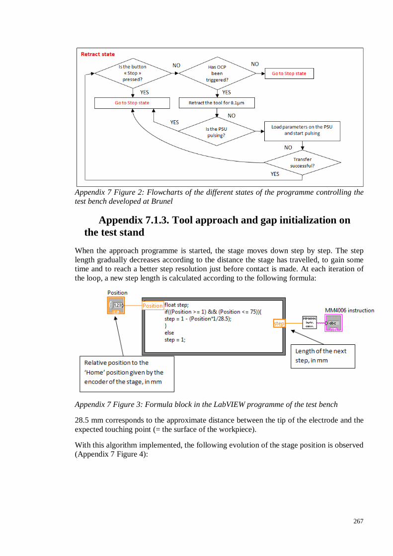
267
Appendix 7 Figure 2: Flowcharts of the different states of the programme controlling the test bench developed at Brunel
Appendix 7.1.3. Tool approach and gap initialization on the test stand
When the approach programme is started, the stage moves down step by step. The step length gradually decreases according to the distance the stage has travelled, to gain some time and to reach a better step resolution just before contact is made. At each iteration of the loop, a new step length is calculated according to the following formula:
Appendix 7 Figure 3: Formula block in the LabVIEW programme of the test bench
28.5 mm corresponds to the approximate distance between the tip of the electrode and the expected touching point (= the surface of the workpiece).
With this algorithm implemented, the following evolution of the stage position is observed (Appendix 7 Figure 4):
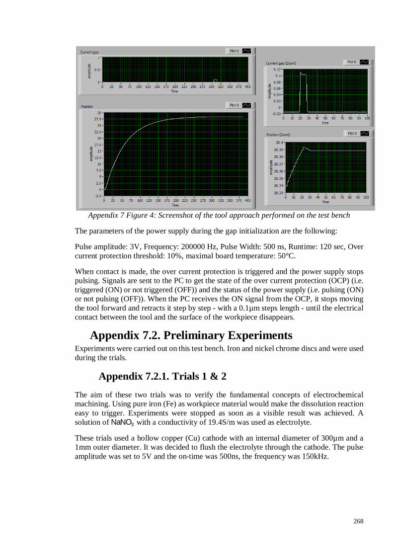
268
Appendix 7 Figure 4: Screenshot of the tool approach performed on the test bench
The parameters of the power supply during the gap initialization are the following:
Pulse amplitude: 3V, Frequency: 200000 Hz, Pulse Width: 500 ns, Runtime: 120 sec, Over current protection threshold: 10%, maximal board temperature: 50°C.
When contact is made, the over current protection is triggered and the power supply stops pulsing. Signals are sent to the PC to get the state of the over current protection (OCP) (i.e. triggered (ON) or not triggered (OFF)) and the status of the power supply (i.e. pulsing (ON) or not pulsing (OFF)). When the PC receives the ON signal from the OCP, it stops moving the tool forward and retracts it step by step - with a 0.1µm steps length - until the electrical contact between the tool and the surface of the workpiece disappears.
Appendix 7.2. Preliminary Experiments Experiments were carried out on this test bench. Iron and nickel chrome discs and were used during the trials.
Appendix 7.2.1. Trials 1 & 2
The aim of these two trials was to verify the fundamental concepts of electrochemical machining. Using pure iron (Fe) as workpiece material would make the dissolution reaction easy to trigger. Experiments were stopped as soon as a visible result was achieved. A solution of NaNO with a conductivity of 19.4S/m was used as electrolyte.
These trials used a hollow copper (Cu) cathode with an internal diameter of 300µm and a 1mm outer diameter. It was decided to flush the electrolyte through the cathode. The pulse amplitude was set to 5V and the on-time was 500ns, the frequency was 150kHz.

269
Appendix 7 Figure 5: Surface of the workpiece in trial 1
Machining around the annulus of the cathode was clearly visible (Appendix 7 Figure 6). There was a central portion that had less machining as this was the area in the centre of the tube and hence the gap to the active portion of the cathode is larger.
The microscope measurements showed that the external diameter of the machined area was 1.030mm and the internal diameter was 0.248mm
Appendix 7 Figure 6: Surface of the workpiece in trial 2
A similar result was achieved with this part when compared to what was achieved in Trial 2. The measurements taken from the microscope images gave an external diameter of 1.093mm and an internal diameter of 0.354mm. The depth of machining was measured as 0.492mm with the microscope. As it can be seen on the images there is a portion of the circle that was not machined, this may have been due to cathode damage.
Appendix 7.2.2. Trials 3 & 4
These trials used a material expected to be more difficult to machine: the workpiece material was 18NiCr6, which contains chromium. Chromium is known for creating a passivation layer which prevents the electro-dissolution reaction from occurring.
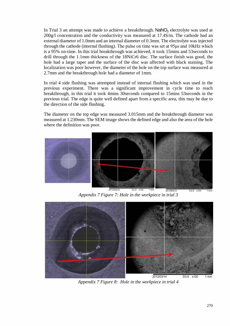
270
In Trial 3 an attempt was made to achieve a breakthrough. NaNO electrolyte was used at 200g/l concentration and the conductivity was measured at 17.4S/m. The cathode had an external diameter of 1.0mm and an internal diameter of 0.3mm. The electrolyte was injected through the cathode (internal flushing). The pulse on time was set at 95μs and 10kHz which is a 95% on-time. In this trial breakthrough was achieved, it took 15mins and 53seconds to drill through the 1.1mm thickness of the 18NiCr6 disc. The surface finish was good, the hole had a large taper and the surface of the disc was affected with black staining. The localization was poor however, the diameter of the hole on the top surface was measured at 2.7mm and the breakthrough hole had a diameter of 1mm.
In trial 4 side flushing was attempted instead of internal flushing which was used in the previous experiment. There was a significant improvement in cycle time to reach breakthrough, in this trial it took 4mins 30seconds compared to 15mins 53seconds in the previous trial. The edge is quite well defined apart from a specific area, this may be due to the direction of the side flushing.
The diameter on the top edge was measured 3.015mm and the breakthrough diameter was measured at 1.230mm. The SEM image shows the defined edge and also the area of the hole where the definition was poor.
Appendix 7 Figure 7: Hole in the workpiece in trial 3
Appendix 7 Figure 8: Hole in the workpiece in trial 4

271
Appendix 7.2.3. Trial 5
In this trial a Tungsten Carbide cathode was used instead of the Copper tube that was used in the previous trials. The external diameter was 0.5mm with an internal diameter of 0.2mm. The electrolyte was NaNO at a concentration of 200g/l. The processing parameters were the same as those used in trial 4. Side flushing was used.
Breakthrough was achieved in a cycle time of 6minutes 29seconds. The process was allowed to run for a further minute to attempt to have a cleaner breakthrough. The microscope image below clearly shows that the extended time at breakthrough definitely improved the quality of the exit hole. The hole is also less tapered as there was time to open out the bottom of the hole. The diameter of the hole was measured at 1.269mm which gives a radial gap of 0.38mm. The SEM image shows the hole produced and it is clear that the walls are vertical, there is very little taper in comparison to some of the previous trials. The SEM image (Appendix 7 Figure 9) below shows a view of the hole to the right hand side of the hole shown in the first SEM image. It shows very little taper and a smooth radius at the edge of the hole.
Appendix 7 Figure 9: Hole in the workpiece in trial 5
Appendix 7.2.4. Trial 6
In this trial a solid Tungsten Carbide cathode with 0.4mm external diameter was used. This was a repeat of the previous trial but with a solid cathode. The trial was allowed to run for 11minutes 50 seconds and side flushing was used, breakthrough was achieved however the quality of the exit hole is quite poor. The hole was very well defined the process control showed that approximately 0.2Amps were being used during the process. The external diameter of the defined edge of the hole on the top surface was measured at 0.903mm. This gives a radial gap of approximately 250µm. The SEM image also shows that the hole was well defined and that there was very little taper. Appendix 7 Figure 10 shows the shape of the breakthrough hole and the scale in this image is 200µm. SEM shows that the quality of ECM is good from the appearance of the quality of the machined surface. There is some debris present in the hole, this occurred post process.

272
Appendix 7 Figure 10: Hole in the workpiece in trial 6
Appendix 7.2.5. Trial 7
In this trial the duty cycle was reduced from 95% to 25%. The pulse on time was set at 95µs and the frequency was set at 2.6kHz. The cathode was changed back to the Tungsten Carbide tube with 0.5mm external diameter and 0.2-0.3mm internal diameter with internal flushing. The supply voltage was 10V and the starting gap was 20µm. The process was allowed to run for 11minutes and 34seconds.
The microscope image shows that a high level of polishing was achieved, this should be a result of the pulsing at 25% duty cycle. Breakthrough was not achieved, which was expected since it should have theoretically taken four times longer than for the other trials which were done at 95% duty cycle.
The images show that the surface finish achieved is of a good level, there is evidence of tapering of the hole however this may seem pronounced as the hole is blind. Diameter measurements taken via the microscope show that the diameter on the top surface was 2.331mm at the extremes of the polished surface and 0.912mm at the top of the hole.
Appendix 7 Figure 11: Hole in the workpiece in trial 7

273
Appendix 7.2.6. Trial 8
This trial was run in the same way as trial 7 and the goal was to achieve breakthrough, however this was not possible to achieve it. The process monitoring software showed good depth progress up until 12minutes, after that the process was struggling to achieve more depth. It would move forward trigger OCP then step back and then move forward again. The microscope image shows a well-defined hole, the diameter measurement indicates that the diameter was between 1.240mm and 1.067mm and the cathode had an external diameter of 0.5mm. The SEM image shows a well-defined hole, the surface finish is at an acceptable level, the degree of taper does not seem too large.
Appendix 7 Figure 12: Hole in the workpiece in trial 8
Appendix 7.2.7. Conclusions and discussion for the preliminary experimental work at Brunel
The work carried out has shown that it is possible to remove material using nanosecond and microsecond pulses using the PSU developed by VOX-power and IT Sligo. Three different electrolytes were used in the experimental work, Sodium Chloride, Sodium Nitrate, and Phosphoric Acid in all instances material removal was observed, however Sodium Nitrate appeared to work quite well.
Through holes were produced in NiCr discs using NaNO electrolyte at 10kHz. Cycle time increases significantly when we go from a duty cycle of 95% (close to DC) to 25%. In our examples it appeared to go from about 3 minutes to 12 minutes for the same depth reached. This makes sense since the temporal mean value of the current supplied to the gap is approximately 4 times smaller at 25% duty cycle than at 95%.
The quality of the machining process was quite good from a surface finish point of view. However there were issues around localisation as the side gap between the cathode diameter and the workpiece hole was in the region of 200-350 µm. This can be explained by the fact that the voltage applied was close to DC and that the frequency was very low with respect to what was found in the literature. Coating of the cathodes should result in improved localization and less tapering of the holes. It could also be confirmed that when using a voltage higher than 8V, the cathode would start to wear.

274
Passivation issues were observed and needed to be investigated further to understand how these could be overcome. The work also highlighted that rotation of the cathode may also have a significant impact on the process as it will aid flushing and will therefore reduce the chances for OCP to occur. The process showed that for a 25% duty cycle and a tubular cathode with an external diameter of 0.5mm and an internal diameter of 0.2-0.3mm and internal flushing that it was difficult to machine to a depth greater than 0.8mm. This could be explained by the pressure building up the deeper the tool is fed.
The trials showed that it Fe reacts better than NiCr to the process when nanosecond pulses are used. We found that internal flushing appeared to give better localization and allowed material removal, however we also saw with NiCr parts that side flushing was quite effective also especially at 95% duty cycles when using NaNO . Coating of the cathode is expected to give better localization and to reduce the tapering effect of the process, it should also result in a more defined hole edge.
The process has highlighted that there is a need to understand how NiCr parts react to nanosecond pulses and at what frequency and duty cycle the process starts to remove material. It is necessary to understand the electrochemistry of the process for the set-up where 18NiCr6 workpieces are used with NaNO electrolyte and Tungsten Carbide cathodes.
Sodium Chloride, Sodium Nitrate, and Phosphoric acid were used during the trials. NaNO appeared to work quite well for the 18NiCr6 and Fe parts. The quality of the ECM was quite good on the 18NiCr6 parts with NaNO .
It has also been observed that allowing the process to run after breakthrough allows a better shape of the breakthrough hole.
Fe discs appear to react better than 18NiCr6 discs when nanosecond pulses are used (e.g. 500ns 150kHz) in that there is visible evidence of machining.

275
Control board of PSU prototype 1
Power board of PSU prototype 1

276
OCP board of PSU prototype 1
Control board of PSU prototype 2
Power board of PSU prototype 2

277
OCP board of PSU prototype 2
Control board of PSU prototype 3

278
Power board of PSU prototype 3

279
OCP board of PSU prototype 3

280
Appendix 8. PSU MODES
- Negative voltage during pulse on-time: SW2, SW3, SW_pulse are ON SW1, SW4, SW_offtime are OFF - Positive offset during pulse off-time: SW2, SW3, SW_offtime are ON SW1, SW4, SW_pulse are OFF
N°7
- Negative voltage during pulse on-time: SW2, SW3, SW_pulse are ON SW1, SW4, SW_offtime are OFF - Negative offset during pulse off-time: SW1, SW4, SW_offtime are ON SW2, SW3, SW_pulse are OFF
N°8
Negative DC voltage. No off-time. SW pulse, SW2 and SW3 all forced ON while SW1, SW4, SW_offtime are OFF
N°6 N°5
Negative voltage during pulse on-time: SW2, SW3, SW_pulse are ON SW1, SW4, SW_offtime are OFF - No offset during pulse off-time: SW1, SW4, SW_pulse are OFF SW2, SW3, SW_offtime are OFF
Positive voltage during pulse on-time: SW1, SW4, SW_pulse are ON SW2, SW3, SW_offtime are OFF Positive offset during pulse off-time: SW2, SW3, SW_offtime are ON SW1, SW4, SW_pulse are OFF
N°4
Positive DC voltage. No off-time. SW pulse, SW1 and SW4 all forced ON while SW2, SW3, SW_offtime are OFF
N°2 N°1
- Positive voltage during pulse on-time: SW1, SW4, SW_pulse are ON SW2, SW3, SW_offtime are OFF - No offset during pulse off-time: SW1, SW4, SW_pulse are OFF SW2, SW3, SW_offtime are OFF
- Positive voltage during pulse on-time: SW1, SW4, SW_pulse are ON SW2, SW3, SW_offtime are OFF - Negative offset during pulse off-time: SW1, SW4, SW_offtime are ON SW2, SW3, SW_pulse are OFF
N°3
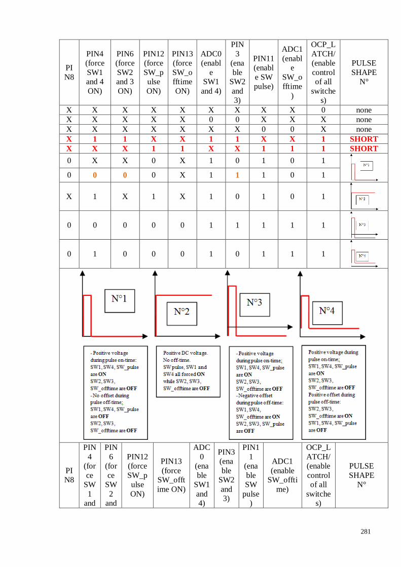
281
PIN8
PIN4 (force SW1 and 4 ON)
PIN6 (force SW2 and 3 ON)
PIN12 (force SW_pulse ON)
PIN13 (force SW_offtime ON)
ADC0 (enabl
e SW1
and 4)
PIN3
(enable
SW2 and 3)
PIN11 (enable SW pulse)
ADC1 (enabl
e SW_offtime
)
OCP_LATCH/ (enable control of all
switches)
PULSE SHAPE
N°
X X X X X X X X X 0 none X X X X X 0 0 X X X none X X X X X X X 0 0 X none X 1 1 X X 1 1 X X 1 SHORT X X X 1 1 X X 1 1 1 SHORT 0 X X 0 X 1 0 1 0 1
0 0 0 0 X 1 1 1 0 1
X 1 X 1 X 1 0 1 0 1
0 0 0 0 0 1 1 1 1 1
0 1 0 0 0 1 0 1 1 1
PIN8
PIN4
(force
SW1
and
PIN6
(force
SW2
and
PIN12 (force SW_pulse ON)
PIN13 (force
SW_offtime ON)
ADC0
(enable
SW1 and 4)
PIN3 (enable
SW2 and 3)
PIN11
(enable SW
pulse)
ADC1 (enable
SW_offtime)
OCP_LATCH/ (enable control of all
switches)
PULSE SHAPE
N°

282
4 ON
)
3 ON
) 1 X X 0 X 0 1 1 0 1
1 0 0 0 X 1 1 1 0 1
X X 1 1 X 0 1 0 0 1
1 0 0 0 0 1 1 1 1 1
1 X 1 0 0 0 1 1 1 1