Embed Size (px)
Citation preview
Fujifilm has developed a sensor film named “EXCLEAR” for touch panels using silver halide photographic technology. This sensor film comprises a conductive silver mesh pattern on both sides of a thin PET film, and a thin transparent sensor. Earlier, indium tin oxide (ITO) was mainly used as the sensor film for the touch panel; however, its conductivity was insufficient for the application to large-size touch panels. Moreover, it tends to easily crack if bent. Furthermore, the supply of indium is limited, which made it a major concern. ITO is resisted as a specific chemical substance. Therefore, there was a need for alternative materials for constructing the sensor film. “EXCLEAR” is a novel sensor film that overcomes these issues related to ITO and responds to the market demand.
Abstract
1. Introduction
Touch sensors are being increasingly used for not only mobiles devices including smartphones and tablets but also laptops. As a transparent conductive film for touch panel, indium tin oxide (ITO) has been mainly used, but various problems are emerging. As touch panels are getting larger, ITO’s conductivity is becoming insufficient. It is particularly not enough for 10-inch or larger touch panels. ITO also does not quite fulfill diversifying needs, such as pen input and enhanced touch performance. In addition, indium, which is a material of ITO, is rare metal and the supply is likely to be limited. The production load is high due to a gas phase process including sputtering. Therefore, a, alternative material is required.
As an alternative sensor material for an ITO film, a metal mesh film and other non-ITO films are attracting attention. In the touch sensor market, expected to be constantly growing, non-ITO films are becoming widely used as a key material for large-size touch panels. In 2014, the non-ITO film market size was 1.72 million m2. In 2016, it was expected to reach 4
million m2 (2.3 folds in two years) (Fig. 1)1).On this backgrounds, we developed EXCLEAR4), a touch
panel sensor film that comprises thin PET with a mesh pattern of several μm wide lines on both sides, using our black and white photographic technology and silver halide photographic technology2), 3) in 2015 (Figs. 2, 3 and 4).
2. Development background
2.1 Touch panel configuration and principle of touch detection
Fig. 5 shows the most commonly used configuration of a touch panel and the principle of touch detection. A panel is divided into cells and each cell is a capacitor consisting of two ITO transparent conductive films and a dielectric layer between them.
A top ITO film and a bottom ITO film have patterned electrodes arranged in different directions (X direction or Y direction). One electrode scans a pulse signal and the other electrode senses it to read a change in the capacitance in a touched position and detect the position.
Development of a Thin Double-sided Sensor Film “EXCLEAR” for Touch Panels via Silver Halide Photographic Technology
Akira ICHIKI*,Yuichi SHIRASAKI*,Tadashi ITO**, Tadahiro SORORI***,and Tadahiro KEGASAWA****
Synthetic Organic Chemistry LaboratoriesResearch & Development Management HeadquartersFUJIFILM CorporationUshijima, Kaisei-machi, Ashigarakami-gun, Kanagawa 258-8577, JapanFrontier Core-Technology Laboratories Research & Development Management HeadquartersFUJIFILM CorporationUshijima, Kaisei-machi, Ashigarakami-gun, Kanagawa 258-8577, Japan
***
****
Original paper(Received December 19, 2016)*
**
Highly Functional Materials Research Laboratories Research & Development Management HeadquartersFUJIFILM CorporationNakanuma, Minamiashigara, Kanagawa250-0193, JapanHighly Functional Materials Research Laboratories Research & Development Management HeadquartersFUJIFILM CorporationUshijima, Kaisei-machi, Ashigarakami-gun, Kanagawa 258-8577, Japan
48 Development of a Thin Double-sided Sensor Film “EXCLEAR” for Touch Panels via Silver Halide Photographic Technology
2.2 Problems of medium- to large-size panel sensorsThe percentages of medium to large sizes (10 to 24 inches)
in all the touch panels are expected to rise5) as demand for tablets is growing and touch panels are increasingly introduced to laptops and all-in-one computers.
When the size of a touch panel is increased, the number of detection points is increased. This means that the scan rate to store an electric charge in each cell must be increased, and the electrode resistance must be reduced. For a 10-inch or larger panel, there is concern that the conductivity of an ITO fi lm will be insuffi cient.
In addition, when the size of a touch panel is increased, the production yield tends to decline as misalignment occurs more frequently in the process of bonding the conductive fi lms. For this reason, highly productive modularization process is required.
2.3 Demand for alternatives for ITOIndium used for ITO fi lms is rare metal and the supply is
likely to be limited. Furthermore, ITO is listed as a specifi ed chemical substance in recent years. It is not desirable to use ITO because of safety.
There is also a concern that the process load, such as (1) gas-phase fi lm forming process, like sputtering, is required, (2) the photolithography process for patterning is complicated, and (3) separate process for peripheral wiring is needed, is high for the sensor production using ITO fi lm.
3. Features of EXCLEAR touch panel sensor
3.1 Confi guration of EXCLEAREXCLEAR is provided with conductivity by silver mesh
patterning. Fig. 6 shows a schematic diagram of a silver mesh pattern. A silver mesh pattern is formed on both sides of the transparent base. Each pattern consists of (1) sensor electrodes and (2) trace lines connected to the sensor electrodes. The electrodes (1) are formed into a pattern with several μm wide lines not to block the LCD image below the sensor and
Fig. 1 Schematic of the worldwide market size for transparent conductive fi lms
Fig. 2 Schematic of an example of a touch panel module
Fig. 3 Roll of EXCLEAR Fig. 4 Schematic of the silver mesh patterning
Fig. 5 The principle governing the projected capacitive touch panels to detect touch positions
(a) Dividing the panel into cells (b) Sensor confi guration in each cell (c) An example of input and output electric signals
FUJIFILM RESEARCH & DEVELOPMENT (No.62-2017) 49
not to cause noise. The trace lines (2) are placed in the frame section (outside the visual area). As a thin fl ame is required to maximize the display area, those lines are usually several tens of μm in width (the same number of lines as that of electrodes are placed in parallel several tens of μm apart from each other).
3.2 Patterning processThe silver mesh pattern of EXCLEAR is formed using the
photographic image forming process. Silver halide, a sensi-tive material, is exposed and developed to be converted to metallic silver (developed silver). Fig. 7 shows the overview of the process. Compared with production process using a resist for patterning, this process is simple.
3.3 Comparison with the conventional sensor ITOEXCLEAR has highly conductive silver patterned in the
form of mesh. That provides EXCLEAR with both optical transmission and electric conductivity and reduces the resis-tance to a lower level than that of ITO (Fig. 8).
Furthermore, EXCLEAR has features that conventional sensor ITO does not have. They are simplifi ed touch module process, reduced sensor fi lm thickness (total sensor thickness is 40 μm) and fl exibility. Those features are explained in the sections below.
(1) Simplifi cation of touch module processWe have developed the following two mass-production
technologies (a) and (b) to improve the touch module process
Fig. 6 Illustration of EXCLEAR silver-mesh patterns
Fig. 8 Schematic of the correlation between transmittance and resistance
Fig. 7 Comparison of various conductive processes
50 Development of a Thin Double-sided Sensor Film “EXCLEAR” for Touch Panels via Silver Halide Photographic Technology
and helped ease the production load (Fig. 9).(a) Simultaneous forming of sensor electrodes and trace
linesFor an ITO fi lm, the sensor electrodes are formed fi rst and
then trace lines are formed in separate process. In the case of EXCLEAR, the sensor electrodes and the trace line are simultaneously exposed to form a pattern and the man-hours are reduced.
(b) Mono-sheet sensorIn the modularization process of a touch panel using ITO
fi lms, two patterned ITO conductive fi lms are to be bonded. In this process, misalignment is likely to occur and that increases the production load. In the case of EXCLEAR, patterns are positioned accurately on both sides of the base and that reduces the production load.
(2) Reduction in sensor thicknessCoupled with the use of the mono-sheet sensor, the thinned
base helps EXCLEAR reduce the sensor thickness to 40 μm and that leads to reduction in the thickness and weight of the device (Fig. 10).
(3) FlexibilityThe conventional sensor ITO is liable to crack when bent.
It needs great care in handling during production. EXCLEAR is highly fl exible, thanks to the right choice of the type and amount of binder. It has much higher bend performance
than that of ITO. Fig. 11 shows changes in resistance when EXCLEAR is wound around a 4-mm diameter rod and bent repeatedly. In the case of ITO, a change in the resistance (from the initial level) increases as the number of bending is increased. There are few changes in the resistances with EXCLEAR.
4. Technical features of EXCLEAR
This section explains the newly developed silver halide sensitive material and its process (pattern exposure and development).
4.1 Silver halide sensitive materialThe newly developed sensitive material is made by apply-
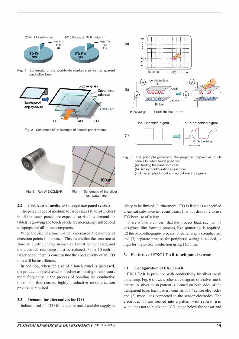
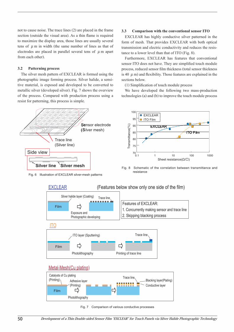
ing several hundreds of nm silver halide particles (silver halide for photography is in several μm) using a polypeptide binder onto a transparent substrate. To give the developed silver high conductivity, an ultrahigh density silver halide sensitive material is newly developed by reducing the percentage of the polypeptide binder, which raises the conductivity between the developed silver particles, to about 1/100 of that used for a conventional photographic sensitive material. (Figs. 12 and 13).
Fig. 9 Schematic of simplifying the touch module process
Fig. 10 Comparison between thickness of the ITO and EXCLEAR fi lms
Fig. 11 Comparison between the fl exibility of EXCLEAR and other materials
FUJIFILM RESEARCH & DEVELOPMENT (No.62-2017) 51
4.2 Pattern exposureSilver halide is a high-effi ciency photo sensor. Various
precision patterns can be formed by pattern exposure on the sensitive material. We have also developed the roll to roll production method to enable pattern exposure with accurate positioning on both sides of the substrate and achieved mono-sheet double-sided sensor.
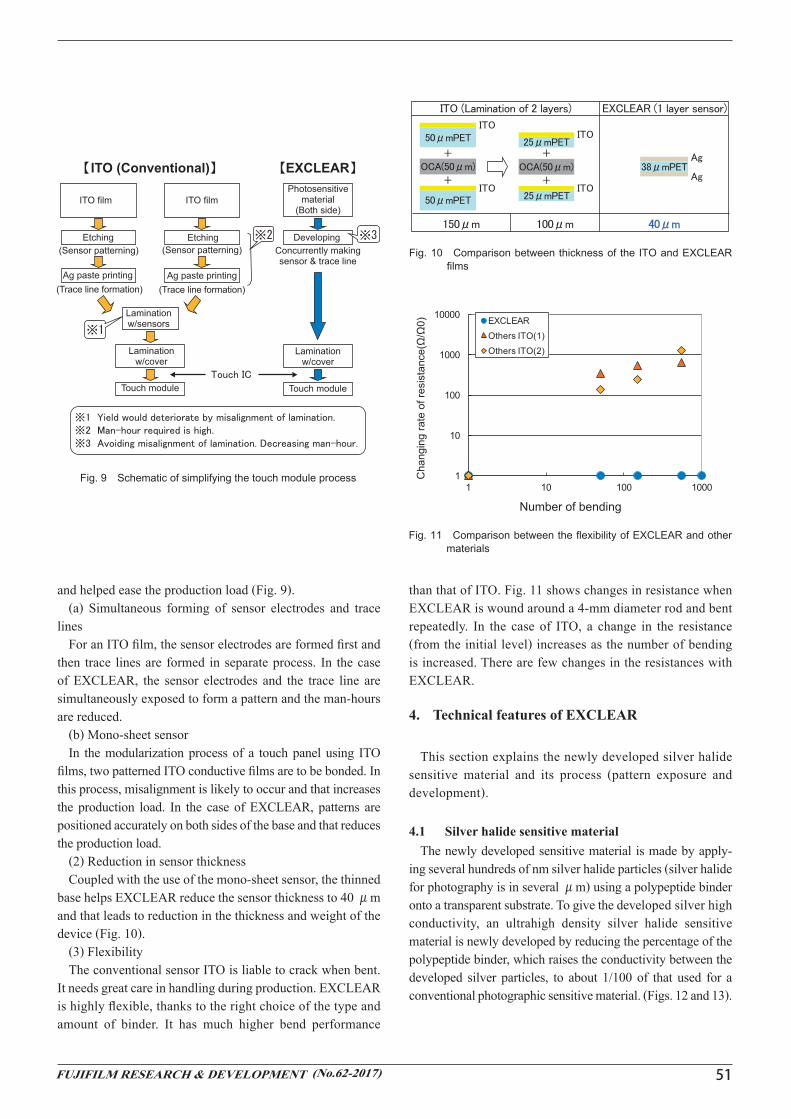
4.3 DevelopmentIn exposed silver halide, latent images (silver nuclei that
trigger development) are formed and they are reduced to silver by the reducing agent in the developing fl uid (Fig. 14). Unde-veloped particles are made soluble by the fi xing agent and removed from the fi lm.
After the chemical development above, EXCLEAR takes on a black tone that comes from the silver fi lament shape. We have also developed a formula of developing fl uid that matches the new sensitive material as below.
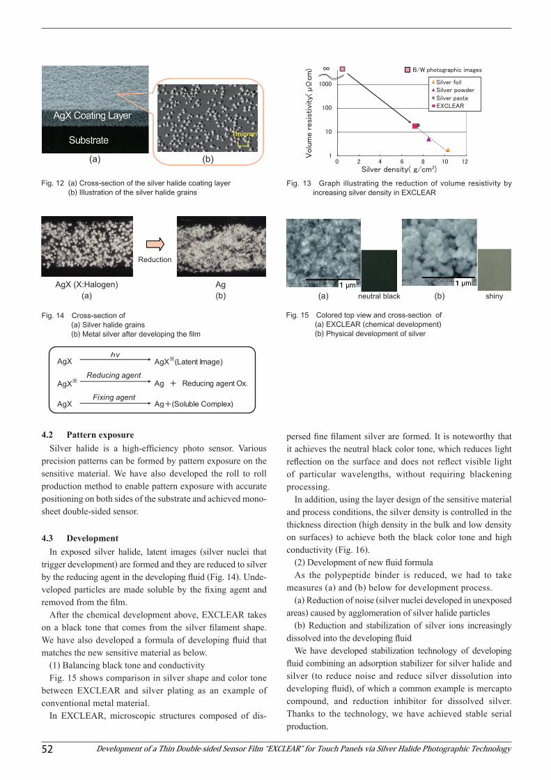
(1) Balancing black tone and conductivityFig. 15 shows comparison in silver shape and color tone
between EXCLEAR and silver plating as an example of conventional metal material.
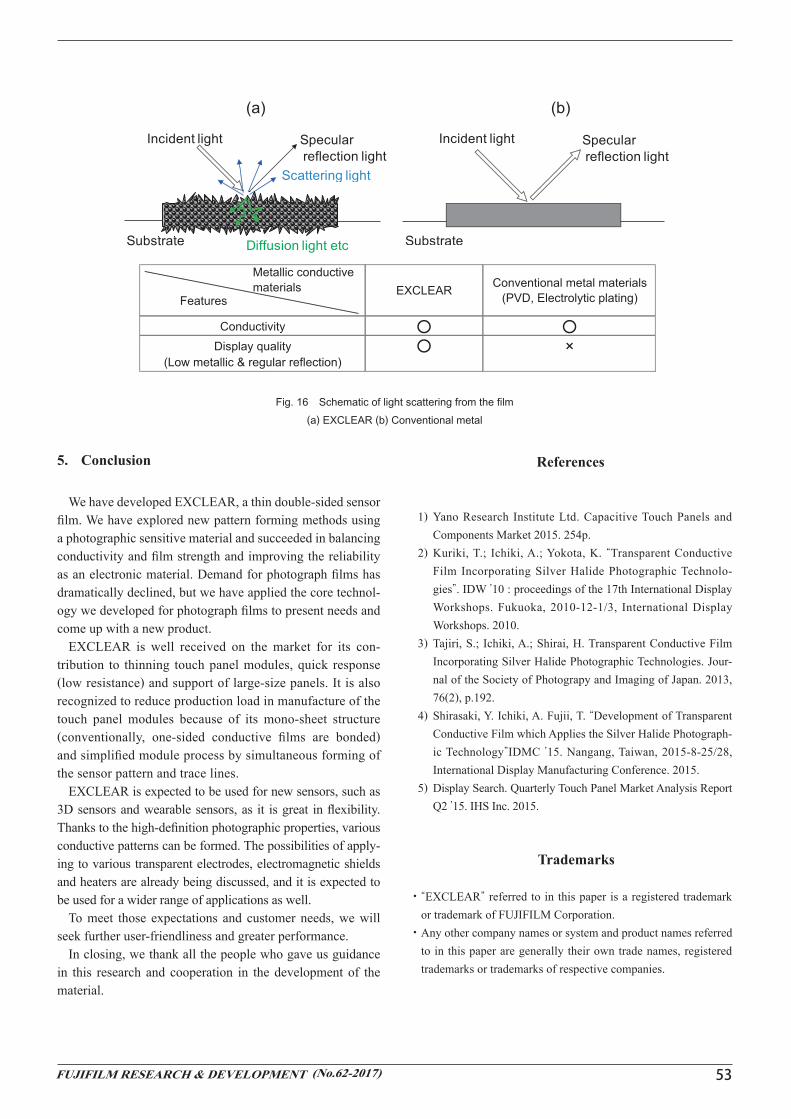
In EXCLEAR, microscopic structures composed of dis-
persed fi ne fi lament silver are formed. It is noteworthy that it achieves the neutral black color tone, which reduces light refl ection on the surface and does not refl ect visible light of particular wavelengths, without requiring blackening processing.
In addition, using the layer design of the sensitive material and process conditions, the silver density is controlled in the thickness direction (high density in the bulk and low density on surfaces) to achieve both the black color tone and high conductivity (Fig. 16).
(2) Development of new fl uid formulaAs the polypeptide binder is reduced, we had to take
measures (a) and (b) below for development process.(a) Reduction of noise (silver nuclei developed in unexposed
areas) caused by agglomeration of silver halide particles(b) Reduction and stabilization of silver ions increasingly
dissolved into the developing fl uidWe have developed stabilization technology of developing
fl uid combining an adsorption stabilizer for silver halide and silver (to reduce noise and reduce silver dissolution into developing fl uid), of which a common example is mercapto compound, and reduction inhibitor for dissolved silver. Thanks to the technology, we have achieved stable serial production.
Silver density( g/cm3)
Volu
me r
esi
stiv
ity(
µΩ
cm) B/W photographic images
0 2 4 86 10 12
10
1
100
1000
∞
Silver foilSilver powderSilver pasteEXCLEAR
Fig. 13 Graph illustrating the reduction of volume resistivity by increasing silver density in EXCLEAR
Fig. 14 Cross-section of (a) Silver halide grains (b) Metal silver after developing the fi lm
Fig. 15 Colored top view and cross-section of (a) EXCLEAR (chemical development) (b) Physical development of silver
Fig. 12 (a) Cross-section of the silver halide coating layer (b) Illustration of the silver halide grains
52 Development of a Thin Double-sided Sensor Film “EXCLEAR” for Touch Panels via Silver Halide Photographic Technology
5. Conclusion
We have developed EXCLEAR, a thin double-sided sensor fi lm. We have explored new pattern forming methods using a photographic sensitive material and succeeded in balancing conductivity and fi lm strength and improving the reliability as an electronic material. Demand for photograph fi lms has dramatically declined, but we have applied the core technol-ogy we developed for photograph fi lms to present needs and come up with a new product.
EXCLEAR is well received on the market for its con-tribution to thinning touch panel modules, quick response (low resistance) and support of large-size panels. It is also recognized to reduce production load in manufacture of the touch panel modules because of its mono-sheet structure (conventionally, one-sided conductive fi lms are bonded) and simplifi ed module process by simultaneous forming of the sensor pattern and trace lines.
EXCLEAR is expected to be used for new sensors, such as 3D sensors and wearable sensors, as it is great in fl exibility. Thanks to the high-defi nition photographic properties, various conductive patterns can be formed. The possibilities of apply-ing to various transparent electrodes, electromagnetic shields and heaters are already being discussed, and it is expected to be used for a wider range of applications as well.
To meet those expectations and customer needs, we will seek further user-friendliness and greater performance.
In closing, we thank all the people who gave us guidance in this research and cooperation in the development of the material.
References
1) Yano Research Institute Ltd. Capacitive Touch Panels and Components Market 2015. 254p.
2) Kuriki, T.; Ichiki, A.; Yokota, K. “Transparent Conductive Film Incorporating Silver Halide Photographic Technolo-gies”. IDW ’10 : proceedings of the 17th International Display Workshops. Fukuoka, 2010-12-1/3, International Display Workshops. 2010.
3) Tajiri, S.; Ichiki, A.; Shirai, H. Transparent Conductive Film Incorporating Silver Halide Photographic Technologies. Jour-nal of the Society of Photograpy and Imaging of Japan. 2013, 76(2), p.192.
4) Shirasaki, Y. Ichiki, A. Fujii, T. “Development of Transparent Conductive Film which Applies the Silver Halide Photograph-ic Technology”IDMC ’15. Nangang, Taiwan, 2015-8-25/28, International Display Manufacturing Conference. 2015.
5) Display Search. Quarterly Touch Panel Market Analysis Report Q2 ’15. IHS Inc. 2015.
Trademarks
・“EXCLEAR” referred to in this paper is a registered trademark or trademark of FUJIFILM Corporation.
・Any other company names or system and product names referred to in this paper are generally their own trade names, registered trademarks or trademarks of respective companies.
Fig. 16 Schematic of light scattering from the fi lm(a) EXCLEAR (b) Conventional metal
FUJIFILM RESEARCH & DEVELOPMENT (No.62-2017) 53


![Integrating technology2[3]](https://img.pdfslide.us/doc/110x75/54972061b47959384d8b50dc/integrating-technology23.jpg)