Embed Size (px)
Citation preview

Development of a systematic recipe set for processing SU8-5photoresist
Deng-Huei Hwang*, Yi-Chung Lo** and Kanping Chin*
*Dept. of Mechanical Engineering, National Chiao-Tung University, Hsinchu, Taiwan
**Synchrotron Radiation Research Center, Research Division, Hsinchu, Taiwan
ABSTRACT
In the current study, a systematic recipe set was developed for processing SU8-5 photoresist in order to fabricate a
microaccelerometer with high-aspect-ratio structure by UV-LIGA process. The disclosed recipe set comprises a series
of relative recipes for processing SU8-5, including spin speed, soft bake, exposure dose, post exposure bake and
developing time. The recipe set is capable of processing SU8-5 film with thickness from 5µm to 80µm. General hot
plate, Karl Süss Gyrset spinner RC8 CT62 (spin coater) and MJB3 exposure aligner which all belongs to the frequently
adopted equipments in the traditional IC fab, were used to explore these recipes. To verify these recipes, the SU8-5
micromold fabricated according to the presented recipe set is employed to electroplate the structure of the biaxial
microaccelerometer with critical dimension of 4x20x500µm. The detail and most effective process parameters
described in this systematic recipe set promote the beginner to process SU8-5 and fabricate the SU8-5 micromold. In
addition, various failure reasons due to adopting the improper recipes are also discussed to provide the guide line for the
reader to develop and approach their own proper recipe to process SU8-5.
Keywords: UV-LIGA, SU8, microaccelerometer;
1. INTRODUCTION
MEMS comprising micro structures with the high-aspect-ratio had been broadly studied in recent years by many
researchers who therefore develop various kinds of approaches to meet the requirement. However, since the
conventional equipment such as the spin coater and the UV-aligner are available in the traditional IC lab to process SU8
photoresist [1], UV-LIGA process using SU8 photoresist is accordingly became one of the most popular approaches
been adopted to form a micromold for electroplating the microstructure [2~5].
**Corresponding Author: e-mail: [email protected], fax: +886-3-578-9816, phone: +886-3-578-0281ext7311
Address: No 1 R&D Rd VI, Science Industrial Park, Hsinchu 300, Taiwan, R.O.C

Though, there are many publications regarding to the process of SU8 [6~8]. To our own knowledge, however, a
systematic approach including detail recipe for processing the SU8 is still lack. Thus, in this paper, we aim at
developing a systematic recipe, which can be easily utilized by other researches to process NANO♥ EPON SU8-5
photoresist in forming films with thickness ranged from 5 to 80 µm [9]. In the present study, we demonstrate that the
SU8 film is used as a micromold to electroplate our newly proposed microaccelerometer structure, as shown in Figure 1.
The developed recipe regarding to spin speed, soft bake, exposure dose, post exposure bake and developing time are all
presented in detail which are able to be ready adopted or checked by other investigator. In addition, a microstructure
with dimension of 4×20×500µm is built to verify the presented recipe.
A
B
C DG s
G d
A n cho r F ram e
S e nsing E le c trode P ad
D r iv ing E le c trode P ad
P roof M a ss
M icrobe amM hL
l
2. NANO♥ XP SU8-5
NANO♥ XP SU8-5 is a negative radiation sensitive resist, which is now commercialized by the company MCC (Micro
Chemical Corp.) in USA. According to the information from MCC, SU8-5 contains wt. 52% organic solvent GBL
(gamma-butyrolacton). The range of available thickness for the SU8-5 film is from 125 µm to 15 µm corresponding
to the spin speed from 250 rpm to 1450 rpm of the spin coater. Additionally, the developer used to develop the post-
exposure-baked SU-8 film is an organic solution, which is also supplied by MCC.
3. EXPERIMENT EQUIPMENT
For processing SU8-5, the adopted equipment includes Oven; Karl Süss Gyrset spinner RC8 CT62 (spin coater); Karl
Süss MJB3 exposure aligner having illumination intensities of 10 mJ/cm2 for 405 nm, and of 17 mJ/cm2 for 360 nm
wavelength; and normal Hotplates. In addition, :α-stepper; Micrometer; Optical microscope; and SEM are employed
to inspect SU8-5 patterned film.
Figure 1(a). Schematic diagram of the proposedbiaxial microaccelerometer.
Figure 1(b). Elevation view of the biaxialmicroaccelerometer.

4. FABRICATION
In this paper, the employed substrate is a silicon wafer with 4” diameter, and the environment temperature for
processing the SU8-5 photoresist is 24℃. The procedure to pattern the micromold, comprises the following steps:
(1) Dispense the SU-8 photoresist onto the substrate;
Distribute enough SU8-5 manually and to form a uniformly round region covered with SU8 on the silicon substrate
from its center to about 0.6 to 0.8 times diameter, in order to coat films with thickness within the range from 5 to 80 µm.
However, a poor SU8 distribution is happened over the entire substrate surface after spin coating, if dispensed
insufficient or not uniform SU8 on the substrate.
(2) Spin coating;
Spin speed and duration time are two major concerns for coating SU8 film to a demanded thickness on the wafer. The
thickness of the SU8 film is not only related to an adopted spin speed but also its duration time. In general, under the
same spin speed, the SU8 film becomes thinner as the duration time is taken longer. However, for the identical
spinning duration, the film thickness is inversely proportional to the spin speed. Additionally, the uniformity of the
film’s thickness is also affected by the duration time. That is, an insufficient spinning duration will cause SU8
transiently distributed on the substrate. Thereby, a thickness variation of the coated SU8 film appears. Figure 2, lists
the relation between the SU8-5 film thickness and the spin speed, which is similar with that recommended by MCC.
However, it also indicates that, it is difficult to coat precisely a SU8-5 film with thickness over 60µm, since the curve
slope of the film thickness versus the spin speed changes abruptly for spin speed less than 300 rpm. In addition to spin
speed and duration time, environment temperature while processing the SU8-5 is another factor has to be concerned.
Since the viscosity of SU8 decrease as the environment temperature increase. The thickness of the coated SU8 film is
also decreased in higher temperature. It is easy to realize that the relation shown in Figure 2 will be deviated under
different environment temperature.
Spin Speed v.s. Film Thickness
0
20
40
60
80
100
0 500 1,000 1,500 2,000 2,500 3,000
Spin Speed (rpm)
Film
Thi
ckne
ss (m
icro
n)
Figure 2. Spin speed and film thickness.

(3) Soft bake;
Although, MCC has recommended the baking temperature of 90 ~ 95℃ to cure SU8. However, the time required to
soft bake SU8 film with different thickness related to the adopted spin speed is not available. In our work, the soft
bake temperature used in this experiment is kept at 90℃. The SU8-5 is just soft baked by hotplate, but no forced
convection surrounding the SU8 film is imposed to facilitate the solvent evacuation. Further, for avoiding the heat
shock, a filter paper is spaced between wafer and hot plate for about 3 minutes after the initial contact. In addition, the
hotplate has to be well leveled. Otherwise, a tilted hotplate makes the SU8 photoresist to redistribute during soft bake
and a distorted SU8 film is therefore formed on the entire substrate. The relationship regarding to the thickness versus
required time for soft bake is shown in Figure 3, which including the first 3 minutes of using the filter paper as a spacer.
It shows that, for properly curing the SU8 film, there is a linear tendency relation between the thickness and the soft
bake time. In our work, we use tweezers to touch the cured surface of the SU8 film to inspect the film solidity. If the
surface of the cured SU8 film is little deformed by tweezers in gentle touch, the SU8 is cured properly. Otherwise,
there has un-negligible residual solvent in the baked SU8. We find that, an insufficient soft baking cannot properly
cure the SU8, the residual solvent will affect the absorption of the exposure energy for the SU8 in the exposure process.
On the other hand, if the SU8 is over baked, the cracks appeared at the interface between the substrate and the SU8 film
will degrade the adhesiveness. That will make the patterned SU8 film to be lifted off during or after development
process.
Soft Bake Time v .s. Film Thickness
05
101520253035
0 20 40 60 80 100
Film Thickness (micron)
Soft
Bak
e T
ime
(min
iute
)
Figure 3. Soft bake time and film thickness.
(4) Exposure;
To construct the vertical sidewall on the pattern made of SU8, it has to supply enough exposure energy. Otherwise,
insufficient exposure dose cannot offer enough energy to crosslink the exposed polymers in the resin of the SU8. That
results in the exposed SU8 film cannot endure the encroachment from the developer during development and thereby
deforms. Contact printing is adopted for exposure to alleviate the diffraction effect, and a longer exposure time or

higher exposure dose is preferred to process the SU8 film to achieve a well defined structure with vertical sidewall and
sharp corner. Similar to the typical negative photoresist, the relation between the exposure time (dose) and the
thickness of the SU8-5 film tends to a slightly nonlinear, as shown in Figure 4. The curve in Figure 4 indicates the
minimum exposure dose required for the SU8-5 film with different thickness. To achieve a successful exposure, it has
to supply exposure dose higher than that shown in Figure 4 to pattern the SU8. However, an overdose makes the
stripping of the SU8 mold more difficult, after electroplated the metal structure.
Expo sure Time v .s. Film Thickness
05
101520
25303540
0 20 40 60 80 100
Film Th ickn ess (micron)
Exp
osu
re T
ime
(sec
)
Figure 4. Exposure time and film thickness.
(5) Post Exposure Bake (PEB);
Dose of post exposure bake is critical for successfully defining the pattern on the SU8-5 film. For negative photoresist
SU8, PEB is to facilitate the crosslink between the exposed polymers. An insufficient PEB causes the SU8 structure
not strong enough to withstand the encroachment applied by the developer. However, an overdosed PED makes a low
selectivity between an exposed and an unexposed region on the SU8 film during development, thereby distort and
misshape the pattern of the SU8 film. To define a sharp and clear pattern, Figure 5 shows the adopted PEB time at 90
℃ for the SU8-5 film. A break of 3 ~ 5 minutes between PEB and development is necessary to allow a chemical
reaction for crosslinking the exposed polymer in the SU8.

PEB Time v.s. Film Thickness
0
20
40
60
80
100
120
140
0 10 20 30 40 50 60 70 80 90
Film Thickness (micron)
PEB
Tim
e (s
ec)
Figure 5. PEB time and film thickness.
(6) Development
Development is to chemically remove the unexposed portions of the SU8 film. By gentle shaking, the exposed portion
of the SU8 film on the wafer immersed in the developer lifts off completely from the substrate during a primary
development. Fresh developer is used to rinse the wafer has been primary developed for less than 30 seconds to clean
the residual scum on the wafer. Thereafter, compressed dry air or nitrogen is used to blow the residual developer away
from the substrate. However, similar to the typical negative photoresist, SU8 absorbs developer and swells during
development especially when the solvent in the SU8 has not been adequately removed by soft bake, or the develop time
is taken too long. That is, the developer will keep going to encroach on the SU8, and the residual solvent makes the
SU8 absorbing more developer and swelling worse. Thereby, the SU8 pattern is distorted. The purple or deep blue
scum resulting from the encroached SU8 is appeared on the substrate after development. Figure 6 shows the time
adopted for developing the SU8 film, which including the rinse time after the primary development.
D e v e lo p m e n t T im e v .s . F ilm T h ic kn e s s
0
1
2
3
4
5
0 1 0 2 0 3 0 4 0 5 0 6 0 7 0 8 0 9 0
F ilm T h ic kn e s s (m ic ro n )
Dev
elop
men
t Tim
e (m
in)
Figure 6. Development time and film thickness.

5. RESULTS AND DISCUSSION
Figure 7 displays the distorted SU8-5 structure, in which, the swelling structure, the snaking beam and the misshaping
gap are due to the developer absorbing. The scum ( as shown by the arrow of Figure 7 but originally in purple or deep
blue color ) on the substrate nearby the SU8-5 structure is resulted from the ill soft bake and/or the insufficient exposure
dose. The residual solvent in the former makes the SU8 not photosensitive in exposure. However, the later causes
less energy to crrosslink the exposed polymer that inducing the SU8 structure is too weak to resist the developer’s
attack [10]. SU8 structures in Figures 7 and 8 are configured on the identical silicon wafer. In contrast to Figure 7,
structure in Figure 8 indicates that if an incorrect recipe is employed for SU8, the dimension resolution is going to be
sacrificed. When adopting an insufficient exposure dose, the energy transmitted through the SU8 film is not enough to
crosslink the polymer, thereby the encroachment is unable to be avoided during development. Figure 9 shows the
SU8-5 structure having an encroached bottom due to an ill exposure dose.
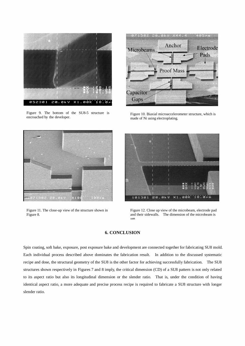
Figures 10, 11 and 12 show the structure of the proposed biaxial microaccelerometer. This structure is made of nickel,
and electroplated by using the SU8-5 mold. The SU8-5 mold has been removed after electroplating. Basically, the
recipes shown in Figures 2 to 6 are employed to fabricate this SU8-5 mold. However, the adopted exposure time for
the SU8 mold used to electroplate the structure shown in Figures 10 ~12 is double to that suggested in Figure 4 .
Figure 7. Gap is misshaped due to the snakingstructure. The original gap dimension on the SU8-5 mold, is 16 µm width × 1000 µm long × 55 µmdeep.
Figure 8. The dimension of gap on the SU8-5mold, is 18 µm width× 1000 µm long × 55 µmdeep.
6. CONCLUSION
Spin coating, soft bake, exposure, post exposure bake and development are connected together for fabricating SU8 mold.
Each individual process described above dominates the fabrication result. In addition to the discussed systematic
recipe and dose, the structural geometry of the SU8 is the other factor for achieving successfully fabrication. The SU8
structures shown respectively in Figures 7 and 8 imply, the critical dimension (CD) of a SU8 pattern is not only related
to its aspect ratio but also its longitudinal dimension or the slender ratio. That is, under the condition of having
identical aspect ratio, a more adequate and precise process recipe is required to fabricate a SU8 structure with longer
slender ratio.
Figure 9. The bottom of the SU8-5 structure isencroached by the developer.
Figure 10. Biaxial microaccelerometer structure, which ismade of Ni using electroplating.
Figure 11. The close-up view of the structure shown inFigure 8.
Figure 12. Close up view of the microbeam, electrode padand their sidewalls. The dimension of the microbeam isµm.

REFERENCES
1. LaBianca N. and Gelorme J. D., “High aspect Ratio Resist For Thick Film Applications,“ SPIE Vol. 2438, pp. 846-
852, 1995.
2. Lorenz et al, “High-aspect-ratio, ultrathick, negative-tone near-UV photoresist and its applications for MEMS“,
Sensors and Actuators, A Vol. 64, pp. 33-39,1998.
3. Lorenz et al, “Mechanical Characterization of a New High-Aspect-Ratio Near UV-Photoresist“, Microelectronic
Engineering Vol. 41/42, pp. 371-374, 1998.
4. Dellmann et al, “Fabrication process of high aspect ratio elastic and SU-8 structures for piezoelectric motor
applications“, Sensors and Actuators, A Vol. 70, pp. 42-47, 1998.
5. Bertsch et al, “Combining Microstereolithography And Thick Resist UV Lithography For 3D Microfabrication“,
Micro Electro Mechanical System, MEMS 98. Proceedings, pp.18-23, 1998.
6. Lorenz, et al, “SU-8: a low-cost negative resist for MEMS“, J. Micromech. Microeng. Vol. 7, pp. 121-124,1997.
7. Despont et al, “High-Aspect-Ratio, Ultrathick, Negative-Tone Near-UV Photoresist For MEMS Applications“,
Micro Electro Mechanical Systems. MEMS 98. Proceedings, pp. 518-522, 1998.
8. Dellmann et al, “Fabrication Process Of High Aspect Ratio Elastic Structures For Piezoelectric Motor
Applications“, TRANSDUCERS ’97, pp. 641-644, 1997.
9. Guérin et al, “Simple And Low Cost Fabrication Of Embeeded Micro-Channels By Using A New Thick-Film
Photoplastic“, TRANSDUCERS ’97, pp. 1419-1422, 1997.
10. David J. Elliott, Integrated Circuit Fabrication Technology, 2nd edition, McGRAW-Hill, 1989.


![MWP phase shifters integrated in PbS-SU8 waveguides · PDF fileMWP phase shifters integrated in PbS-SU8 waveguides ... Marpaung, C. Roeloffzen, R. Heideman, ... [16], SOA based](https://img.pdfslide.us/doc/110x75/5a869ff07f8b9a882e8d11ac/mwp-phase-shifters-integrated-in-pbs-su8-waveguides-phase-shifters-integrated-in.jpg)


![[XP Day Vietnam 2015] XP is not windows XP](https://img.pdfslide.us/doc/110x75/55a69cf71a28abd47d8b4735/xp-day-vietnam-2015-xp-is-not-windows-xp.jpg)

![[XPday.vn] XP? not Windows XP {presentation} (at) [XP Day Vietnam 2015]](https://img.pdfslide.us/doc/110x75/55c4e9e3bb61ebac3f8b47ae/xpdayvn-xp-not-windows-xp-presentation-at-xp-day-vietnam-2015.jpg)