Embed Size (px)
Citation preview
Development of a Design & ManufacturingDevelopment of a Design & ManufacturingEnvironment for Reliable and CostEnvironment for Reliable and Cost --Effective Effective
PCB Embedding TechnologyPCB Embedding Technology

• Introduction
• CAD design tools for embedded components• Thermo mechanical design rules
• The industrialisation of chip embedding• Outlook and business
Outline
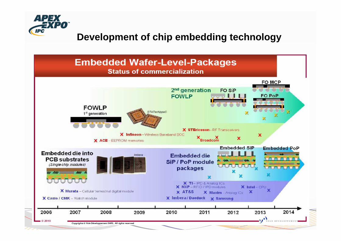
Development of chip embedding technology

• Technology drivers that create large pin count devices
– SoC – more functional density
– SiP – mixed technologies with memory
• Miniaturization approaches used on PCB systems
– Mezzanine boards
– Rigid Flex circuits
– High Density Interconnect • Shrinking pin pitch (< 0.4mm)
• Large pin count devices
– Embedded Passives
– Low pin Actives
• 2G / 3G / 2 MP• GPS / WiFi• Memory• Slim
2008 2009
• 3G / 3.2-MP• GPS / WiFi• More Memory• Slimmer profile• Battery life
Miniaturization Approaches

PCB / IC-Packaging design tool requirements1) Component, layer stack selections
Engineers specify
• Components to be embedded
– “Embed Required” (Hard) or “Embed Optional” (Soft)
– Ensures only qualified components get embedded
• Layers to be used
Embedding concept
• Chip-up, Chip-down
• Face-up, Face-down
• Direct (SMD), Indirect (embedded)
Chip up
Chip Down

• Component to Component / Cavity
• Height checks – gap between component in cavity to adjacent metal layer
• Max cavity area
• Max number of components in cavity
• Vias within cavity area
• Metal to cavity area
• Extended cavity support based on component height
• etc
PCB / IC-Packaging design tool requirements2) Design Rule Checks
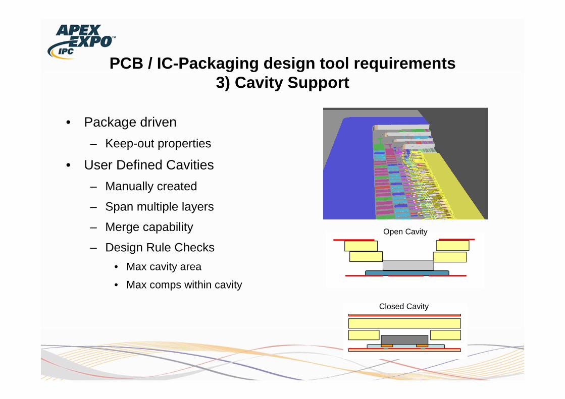
PCB / IC-Packaging design tool requirements 3) Cavity Support
• Package driven
– Keep-out properties
• User Defined Cavities
– Manually created
– Span multiple layers
– Merge capability
– Design Rule Checks
• Max cavity area
• Max comps within cavity
Open Cavity
Closed Cavity

• Constraint driven place and route
– Move components to inner layers
• Don’t put a via through the component!
– Route to embedded components adhering to electrical, physical and manufacturing constraints
• Manufacturing outputs for layers with embedded devices
– ODB++
– etc
Dynamic Design for Assembly guided placement
PCB / IC-Packaging design tool requirements 4) Constraint-Driven Place & Route, Mfg outputs

Cadence
Version: Allegro Beta 16.4
HERMES Support Partner: THALES
Functionality for ECP® Release: Planned Q2, 2011
ECP® component placement between copper layers
ECP® component pads available for via interconnect
ECP® component with pads on top and bottom side
Possibility to flip and/or rotate each ECP® component separately
Component span over several copper layers
Additional layers for ECP® - assembly, glue spots, cavities
Separate assembly output for ECP® components
ODB++ support for ECP®
Gerber/Excellon support for ECP®
Via-in-pad technology
Filled/stacked via support for sequential buildup
Supported Planned Workaround
Checklist for EDA ECP Capability

Modelling of stress & strain in embedded structures
Design rules
FEA analysis
Torsion test with strain measurement
Strain distribution
Failure mechanism
Thermo-Mechanical Assessment Methodology

Various 4-6 layer PCBs embedding daisy-chain dies
• Total thickness : 0.8mm – 1.6mm – 2.0mm• 2 halogen-free base materials
Test Vehicle Overview
Embedded die
Embedded gage
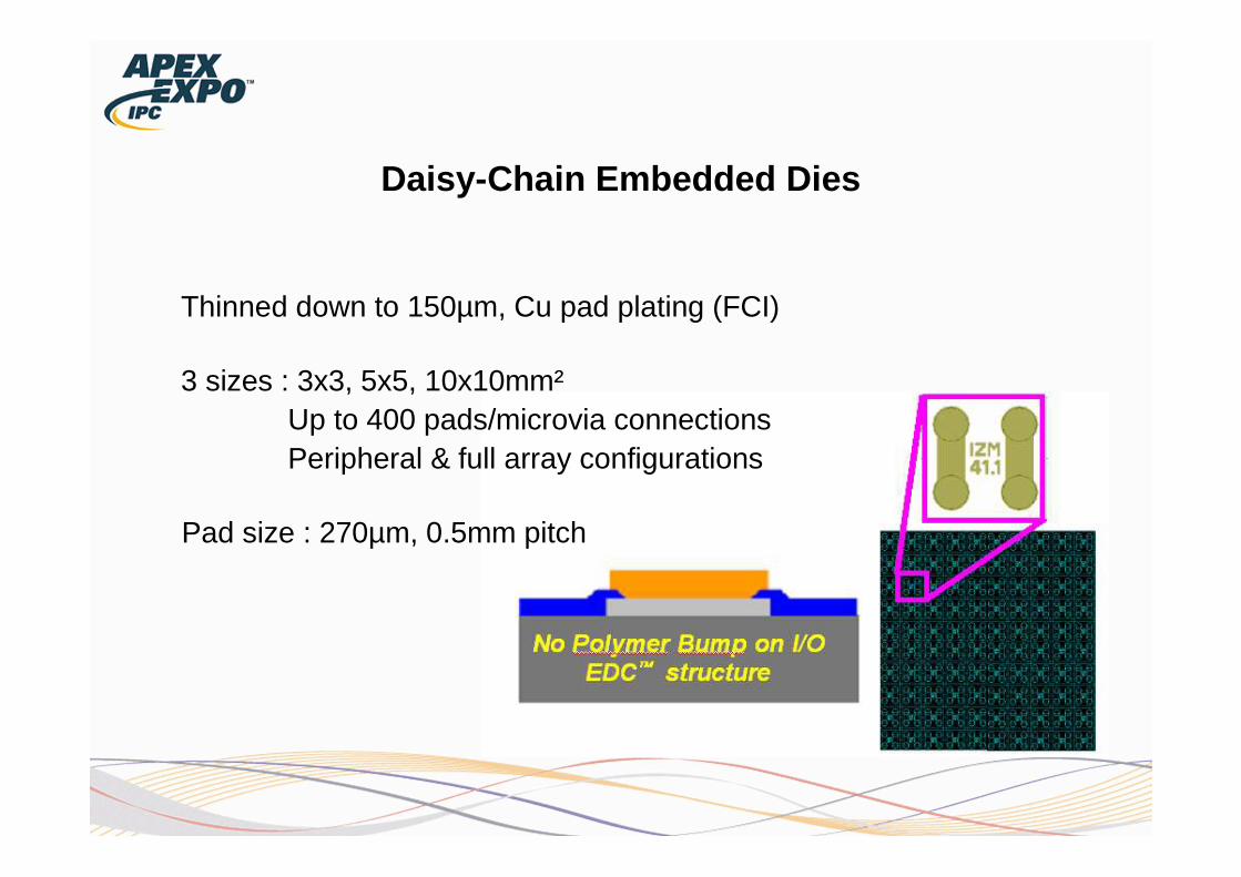
Daisy-Chain Embedded Dies
Thinned down to 150µm, Cu pad plating (FCI)
3 sizes : 3x3, 5x5, 10x10mm²Up to 400 pads/microvia connectionsPeripheral & full array configurations
Pad size : 270µm, 0.5mm pitch

Torsion Testing
Strain gage measurements under repeated torsion cycles
• Angle : -7° / +7°• Temperature : up to 100°C
Embedded Strain Gages
Assembled Strain Gages
h
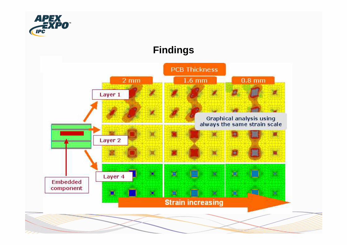
Findings

Sensitivity AnalysisIncidence of various design parameters on strain for embedded
components
Increased strain on Si dies withoverlapping
Overlap vs No overlapInteraction between embeddedand assembled components
0.4mm better for thin boards(<1mm)
No significant effect for thickerboards
0.2mm vs 0.4mmEmbedded core thickness
Higher thickness better0.8mm vs 2.0mmPCB thickness
2116 better1080 vs 2116 pre-preg typeResin content
Material A betterMaterial A vs Material BHalogen-free, high performance
FR4
PCB Base Material
ResultsConditionsDesign Parameter
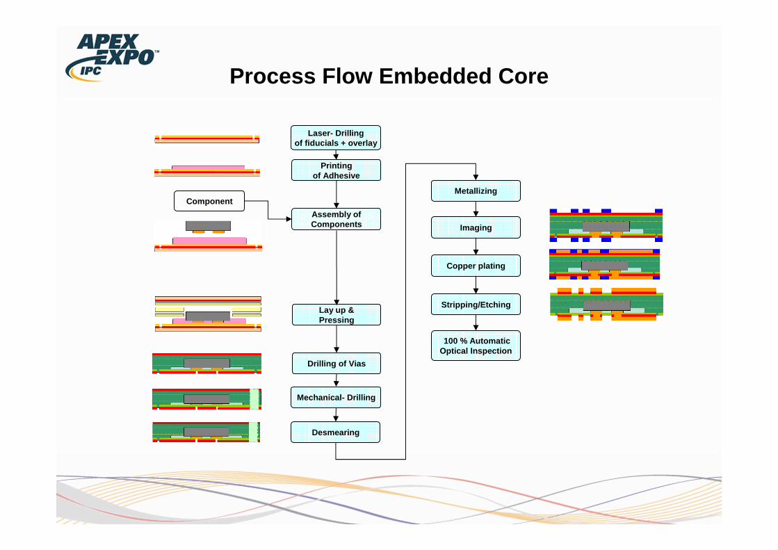
Laser- Drillingof fiducials + overlay
Printingof Adhesive
Assembly ofComponents
Lay up &Pressing
Desmearing
Drilling of Vias
Component
Mechanical- Drilling
Imaging
Copper plating
Stripping/Etching
100 % AutomaticOptical Inspection
Metallizing
Process Flow Embedded Core

• Control of – feature size, shape and volume– By novel 3D scanner for large panels
– determines the thickness and uniformity of the dielectric
Adhesive Printing

• Optical alignment of Flip Chip component– Requires high resolution cameras– Pattern recognition of pad design
• Design– Pad diameter: 150 µm– Minimum pitch : 200 µm– Chip size : 7 x 7 mm
Component Assembly
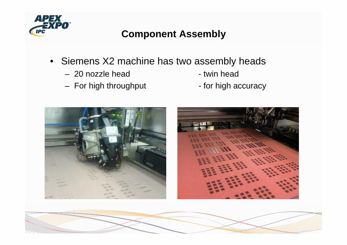
• Siemens X2 machine has two assembly heads– 20 nozzle head - twin head– For high throughput - for high accuracy
Component Assembly
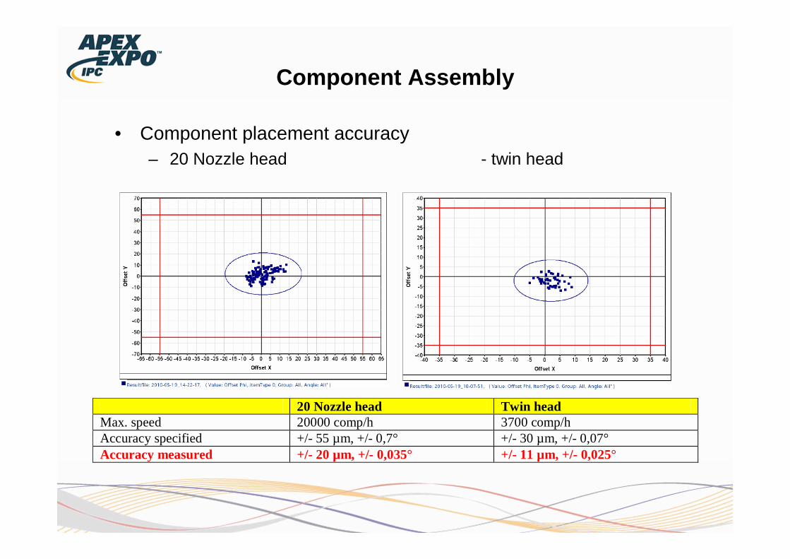
• Component placement accuracy – 20 Nozzle head - twin head
20 Nozzle head Twin head Max. speed 20000 comp/h 3700 comp/h Accuracy specified +/- 55 µm, +/- 0,7° +/- 30 µm, +/- 0,07° Accuracy measured +/- 20 µm, +/- 0,035° +/- 11 µm, +/- 0,025°
Component Assembly

• Exposure with LDI – registration fiducial to pattern
25 µm technology
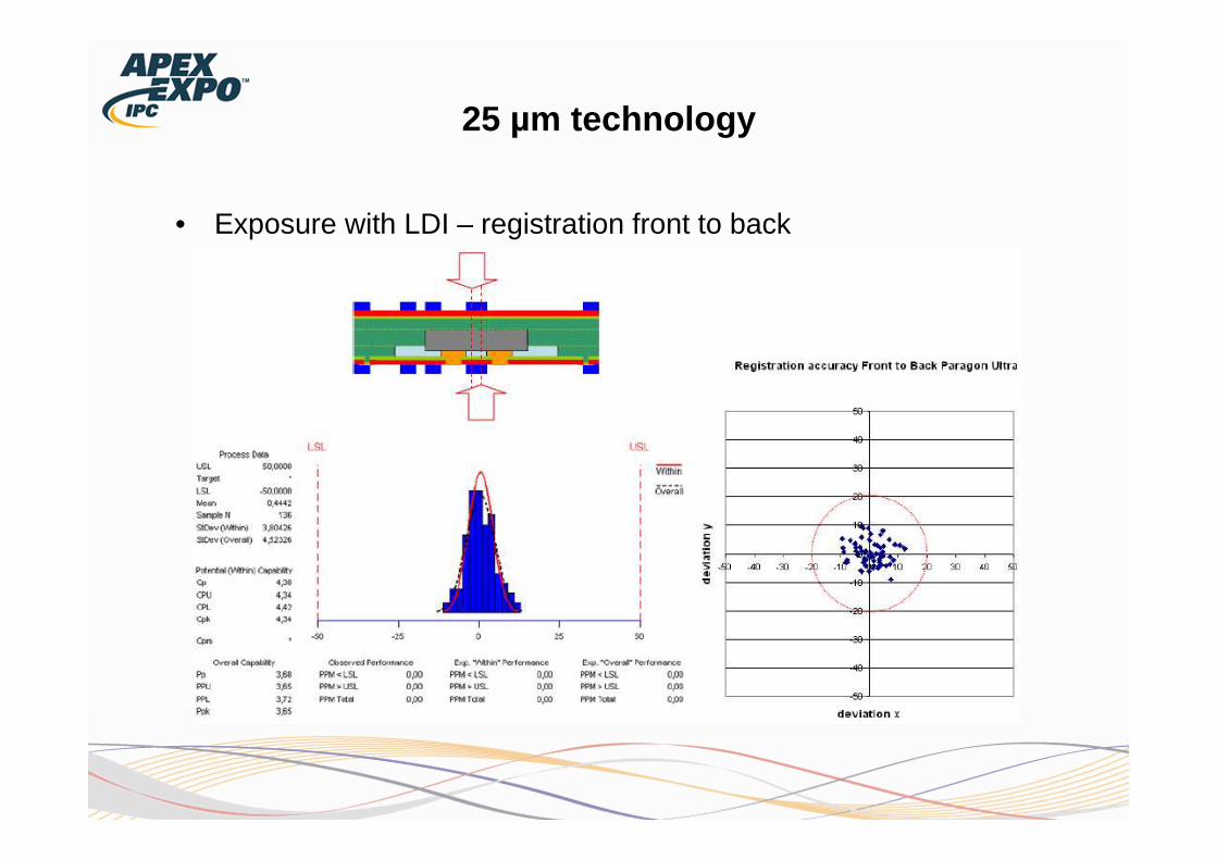
25 µm technology
• Exposure with LDI – registration front to back

• Semi-additive technology – single board plater
– Individual control of parameters of each panel
– Handling of thin cores
– Unique flow system
– Pulse plating for via filling
– Full traceability of process data
– Single piece flow for improved
• Flexibility
• Risk management
25 µm technology
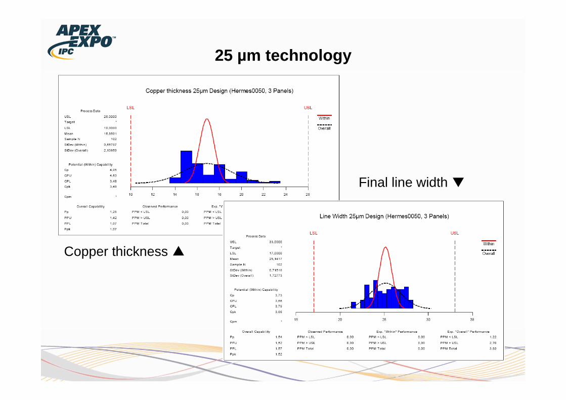
Copper thickness ▲
Final line width ▼
25 µm technology

25 µm technologyDesign of motor management module

Outlook for embedded modulesIndustrialization Roadmap
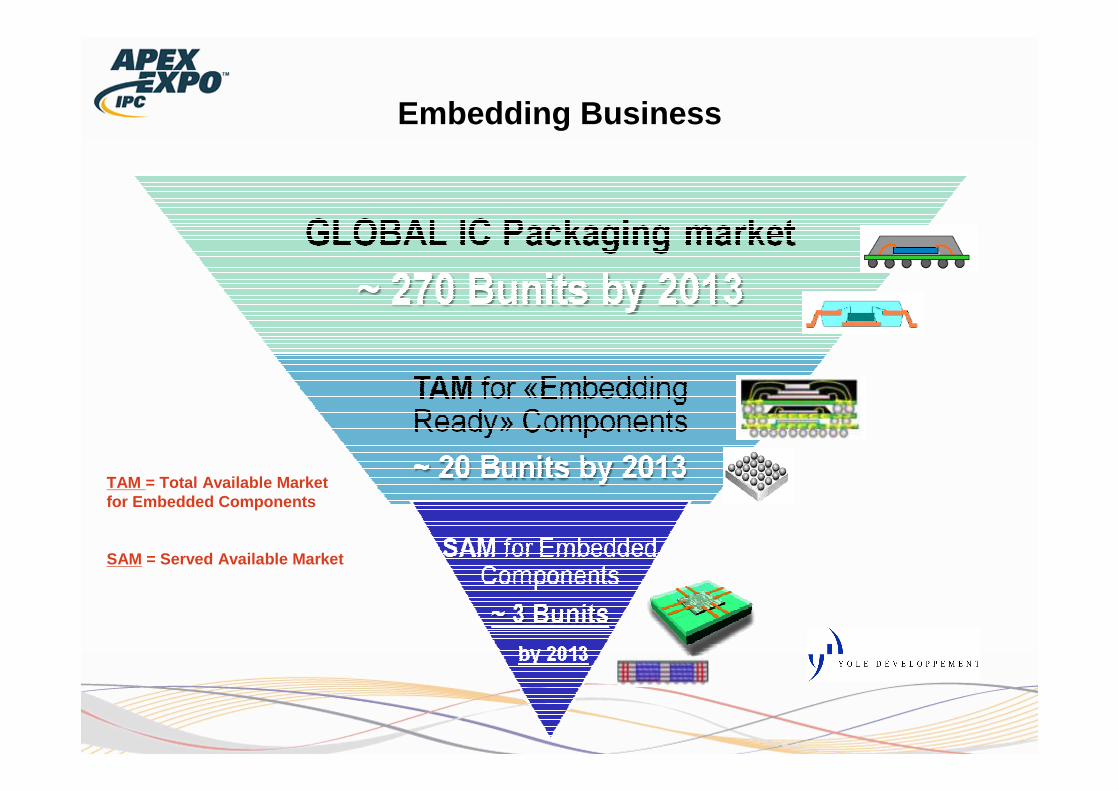
Embedding Business
TAM = Total Available Market for Embedded Components
SAM = Served Available Market
Thank you for your attention
For more information, go to our Hermes website
http://www.hermes-ect.net