Embed Size (px)
Citation preview
TCAD as an integral part of the semiconductormanufacturing environment
(Invited Paper)
Rainer Minixhoferaustriamicrosystems AGSchloss Premstaetten
Unterpremstaetten, AustriaEmail: [email protected]
Abstract- This work shows a new methodology which auto-mates the necessary links between technology computer aideddesign (TCAD) and the semiconductor manufacturing environ-ment to a high extent. Initially a short overview of a typical chainof processes during the fabrication of an integrated circuit isgiven. Furthermore an overview on the relations to the respectivesimulator tools is given.
The interfaces between the fabrication process and simulationare identified and the detailed structure of the interfaces isoutlined. A comprehensive overview over the interactions in thisintegrated system is given as well.
Finally the strengths of such a structured and integratedapproach are demonstrated with a case in a real semiconductorfabrication environment.
I. INTRODUCTION
This work concentrates on technology computer aided de-sign (TCAD) [1] and its integration into the semiconductorfabrication process flow. The use of TCAD is twofold: Firstlyit models the complex flow of semiconductor fabricationsteps ending up with detailed information on geometric shapeand doping profile distribution of a semiconductor devicein scope (like CMOS- or Bipolar-Transistors). Secondly ituses the information of the first step to predict the devicecharacteristics of semiconductor devices leading to circuitsimulation models as implemented in any circuit simulatorlike PSPICE [2], ELDO [3], SPECTRE [4] etc. The setupof such a simulation methodology requires an almost com-pletely documented semiconductor fabrication process flowincluding such fabrication details like angle of incidence ofions implanted in ion implantation process steps, or etch ratedistribution as a function of the local angle of the etched layersurface. Any modern semiconductor fabrication facility main-tains such documentation to an extremely high detail level, butcommercial TCAD simulation software like Synopsys [5] orSilvaco [6] tools need this information in a very specializedformat [7] which cannot be directly deduced from the standardprocess flow documentation. The traditional way of settingup the process- and to some extent also the device TCAD-simulation framework is, entering it by hand, which is ofcourse a source of numerous errors. This work shows a newmethodology with the main target to automate the necessarylinks to the manufacturing environment to a high extent. Afteroutlining the two "worlds" of TCAD and manufacturing in
Section II and Section III and showing the concept used forconnecting them both together in Section IV an example ofa successful implementation of the proposed methodology isgiven in Section V
II. THE PROCESSING CHAIN IN SEMICONDUCTORMANUFACTURING
A. OverviewThe semiconductor industry is starting from the product idea
the following sequential steps occur in a standard integratedcircuit development and production flow [8].
1) Development: Starting from the product idea, the elec-tronic contents of the overall system are developed,leading into a schematic of the electronic circuitry. Fordigital circuitry this development process is similar towriting a software program by using Very High SpeedIntegrated Hardware Description Language (VHDL) asa abstract description of the digital block. The devel-opment of a digital block starts with the specification(operation and timing) and the subsequent descriptionof this specification via a model in VHDL.
2) Design: The integrated circuit is designed starting fromthe schematic, and taking into account the special de-mands of integrated circuits (crosstalk, common sub-strate, etc.). It is state of the art to use ECAD (electroniccomputer aided design) tools to simulate the behaviourof a design as an integrated circuit by using detailedcircuit simulation models and design rules, which arespecific to a process family (technology node) [9].
3) Layout: The resulting integrated circuit is drawn as alayout on the specific layers which are given by thesemiconductor process family (technology node). Thecombination of multiple layers, like implantation masksand etch masks, define the shape and functionality ofthe electronic devices in the integrated circuit [10].
4) Mask-Shop: The layout is post processed to take intoaccount process induced size variations (layer biasing)and constraints on combination of layers (logical combi-nation). The physical mask layers are written from thisdata by using laser- [11] or e-beam [12] equipment.
5) The wafer start material is released at the beginning ofthe process flow into fabrication [13]. In the following
1-4244-0404-5/06/$20.00 © 2006 IEEESISPAD 2006 9
dimensional process- and device-simulation applications.However, the set-up of these TCAD-simulators is highly
complicated and time consuming. Changes in fabrication pro-cedures like parameter optimization of process conditions arenot reflected in simulation with the traditional way of definingthis set-up by hand. Therefore the simulation flow definitionsbecome asynchronous to the semiconductor fabrication veryquickly.The main concept to be considered is to match the sim-
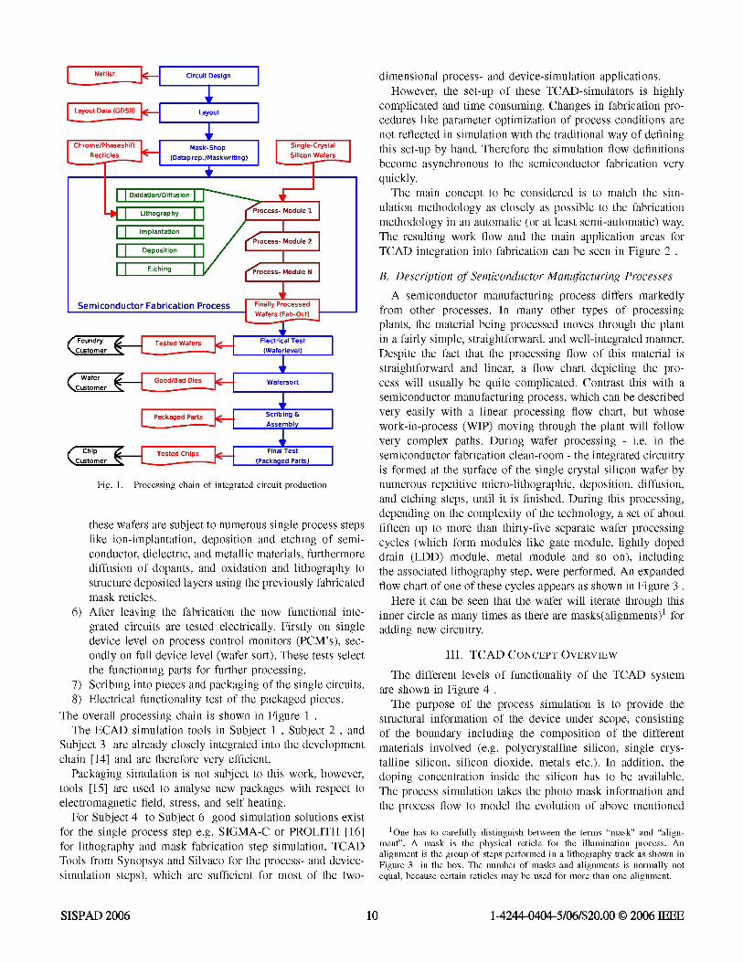
ulation methodology as closely as possible to the fabricationmethodology in an automatic (or at least semi-automatic) way.The resulting work flow and the main application areas forTCAD integration into fabrication can be seen in Figure 2 .
FoundryeCustomer a, r
Wafer~~~~~~~~~~~~Wfeivl
fWafer 4 Good/ad Die WafersortXCustomer
Scirib ing &S|
Chip 4 ! Teste Chip FinalTestxCustomer \c q
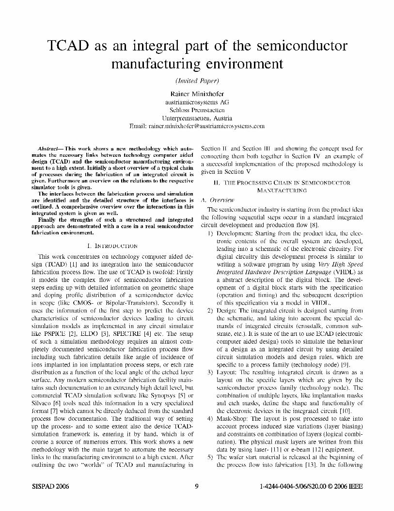
Fig. 1. Processing chain of integrated circuit production
these wafers are subject to numerous single process stepslike ion-implantation, deposition and etching of semi-conductor, dielectric, and metallic materials, furthermorediffusion of dopants, and oxidation and lithography tostructure deposited layers using the previously fabricatedmask reticles.
6) After leaving the fabrication the now functional inte-grated circuits are tested electrically. Firstly on singledevice level on process control monitors (PCM's), sec-ondly on full device level (wafer sort). These tests selectthe functioning parts for further processing.
7) Scribing into pieces and packaging of the single circuits.8) Electrical functionality test of the packaged pieces.
The overall processing chain is shown in Figure 1 .
The ECAD simulation tools in Subject 1 , Subject 2 , andSubject 3 are already closely integrated into the developmentchain [14] and are therefore very efficient.
Packaging simulation is not subject to this work, however,tools [15] are used to analyse new packages with respect toelectromagnetic field, stress, and self heating.
For Subject 4 to Subject 6 good simulation solutions existfor the single process step e.g. SIGMA-C or PROLITH [16]for lithography and mask fabrication step simulation, TCADTools from Synopsys and Silvaco for the process- and device-simulation steps), which are sufficient for most of the two-
B. Description of Semiconductor Manufacturing Processes
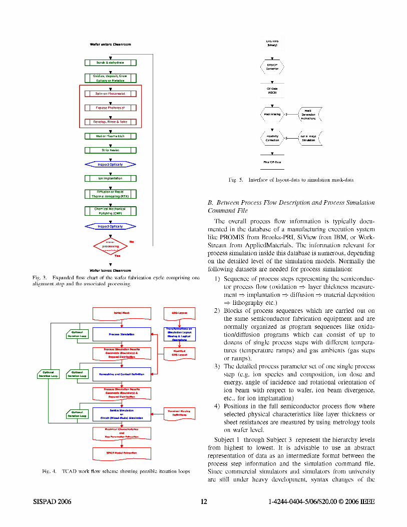
A semiconductor manufacturing process differs markedlyfrom other processes. In many other types of processingplants, the material being processed moves through the plantin a fairly simple, straightforward, and well-integrated manner.Despite the fact that the processing flow of this material isstraightforward and linear, a flow chart depicting the pro-cess will usually be quite complicated. Contrast this with asemiconductor manufacturing process, which can be describedvery easily with a linear processing flow chart, but whosework-in-process (WIP) moving through the plant will followvery complex paths. During wafer processing - i.e. in thesemiconductor fabrication clean-room - the integrated circuitryis formed at the surface of the single crystal silicon wafer bynumerous repetitive micro-lithographic, deposition, diffusion,and etching steps, until it is finished. During this processing,depending on the complexity of the technology, a set of aboutfifteen up to more than thirty-five separate wafer processingcycles (which form modules like gate module, lightly dopeddrain (LDD) module, metal module and so on), includingthe associated lithography step, were performed. An expandedflow chart of one of these cycles appears as shown in Figure 3 .
Here it can be seen that the wafer will iterate through thisinner circle as many times as there are masks(alignments)l foradding new circuitry.
III. TCAD CONCEPT OVERVIEW
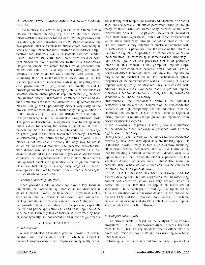
The different levels of functionality of the TCAD systemare shown in Figure 4 .
The purpose of the process simulation is to provide thestructural information of the device under scope, consistingof the boundary including the composition of the differentmaterials involved (e.g. polycrystalline silicon, single crys-talline silicon, silicon dioxide, metals etc.). In addition, thedoping concentration inside the silicon has to be available.The process simulation takes the photo mask information andthe process flow to model the evolution of above mentioned
1One has to carefully distinguish between the terms "mask" and "align-ment". A mask is the physical reticle for the illumination process. Analignment is the group of steps performed in a lithography track as shown inFigure 3 in the box. The number of masks and alignments is normally notequal, because certain reticles may be used for more than one alignment.
1-4244-0404-5/06/$20.00 © 2006 IEEESISPAD 2006 10
Layo0ut lht&f6ce
Layout Transformnations IiilMs
| rocess Sim. Module 2
tchingSim. ess Sm. Mdlodule N|
Semiconductor Process Simulabon |Geomretric (Bounldary) &|Dopand Distribution
niov5ii fifiorfAeo 7- 1Foundry
(Customer
Wafer
(Customer
SPICE Interface
Package Interface
Chip TeskCustomer Pt
Fig. 2. Structure of the semiconductor process flow and its mirror image the TCAD simulation flow. The interfaces between TCAD and semiconductorfabrication are identified as well.
information (boundary and dopant) over the multiple steps ofthe process.The mesh for solving the partial-differential equations (PDEs)typical for the physical and chemical processes occurring dur-ing processing is normally of unstructured type, to model thesteep gradients of the doping distributions with good accuracy,but with a low number of mesh points where the physical fields(doping concentration, point defect concentrations etc.) are notvarying much. A detailed description of a process simulatorcan be found in, e.g., [17]The boundary and dopant information is then used as aninput to describe the electrical behaviour of the device underscope by calculating the potential distribution and the carriertransport phenomena (current concentrations etc.) via solvingthe PDEs describing their physics. A detailed description ofthe underlying principles of a device simulator can be foundin, e.g., [18]Since the requirements on meshes for process and devicesimulations, respectively, are very different, a re-meshingstep is necessary to minimize the numerical error, and thenumber of mesh points necessary for a certain accuracy of thesolution. This re-meshing is normally based on the gradientor difference refinement criteria. In some cases this approachis not sufficient to get a good mesh. The inversion region of aMOSFET channel is a good example for the problems gradientrefinement criteria are facing. However in recent investigationapproaches are outlined to overcome or, at least, to tackle theselimitations [19].
IV. INTEGRATION BETWEEN SEMICONDUCTORFABRICATION AND TCAD
The shaded areas in Figure 2 indicate the different inter-faces identified between "reality" and "simulation".
A. Between Design/Layout as Process Simulation Input
According to the work flow outlined in Section III , thelayout of the masks is one of the two main inputs for processsimulation.Normally this layout is available in GDSII-binary formatwhich can be read by any of the above mentioned commer-cially available TCAD tools. To mirror the activities carriedout in the mask shop this data must undergo the same trans-formations as in reality listed in Subject 4 of Subsection II-A. The "Mask Generation Instructions" define special booleanoperations to modify the mask data in a way that certain effectsof wafer processing are cancelled out. Examples for possiblecorrections like simple mask biasing or proximity corrections.
Figure 5 shows the detailed structure of the identifiedinterface as motivated by the real mask generation and lithog-raphy process. The GDSII data is converted into the ASCIIformatted CIF format (for easier processing) This data is thensubject to boolean and biasing operations as defined by themask generation instructions. To emulate the real shape of thephotoresist a proximity correction is applied and the resultingcontours are written back to a CIF format serving as maskinformation input during the process simulation.
1-4244-0404-5/06/$20.00 © 2006 IEEE
uevice inuerTace
SISPAD 2006 11
Wafer enters Cleanroom
~;es
Wafer leaves Cleanroom
Fig. 3. Expanded flow chart of the wafer fabrication cycle comprising onealignment step and the associated processingg l l ~~~~~~~~~~~~~~~~~~Transomtosa
aptlocess Simulation
l Simulation Layoutl|trato Lop lB rcssS iasing & Logicail
| , l l l l ODe~~~~~~~~~~~~~~~~~~~Q2ratignslil~~~~~~~~~~~~~~~~~~~~~~~~~~ el Ceometric (Boundary) & H C~~~~~DS-Layout
g ~ ~~ ~ ~ ~ ~ ~eehnoand ContatriDefntion lE
(RmInLo
g Optional g rational RmsiLoop ortcDefinitionns
l P~~~~~~~Crcuit (M imulatiode Rsiulation
l C~~~~~~~~~~ecmtricaCh unary)&al Dopand DistriDutionand
FIg 4 TCDwrI lwshmesoigpsilterationloopslll
GDSu-Data(binary)
CIF-Data(ASCII)
< ak Biasing nGnrain
\/ \5ns~~~ntructions
rretio VSimulto
Fig. 5. Interface of layout-data to simulation mask-data
B. Between Process Flow Description and Process SimulationCommand File
The overall process flow information is typically docu-mented in the database of a manufacturing execution systemlike PROMIS from Brooks-PRI, SiView from IBM, or Work-Stream from AppliedMaterials. The information relevant forprocess simulation inside this database is numerous, dependingon the detailed level of the simulation models. Normally thefollowing datasets are needed for process simulation:
1) Sequence of process steps representing the semiconduc-tor process flow (oxidation =* layer thickness measure-ment =# implantation => diffusion => material deposition=> lithography etc.)
2) Blocks of process sequences which are carried out onthe same semiconductor fabrication equipment and arenormally organized as program sequences like oxida-tion/diffusion programs which can consist of up todozens of single process steps with different tempera-tures (temperature ramps) and gas ambients (gas stepsor ramps).
3) The detailed process parameter set of one single processstep (e.g. ion species and composition, ion dose andenergy, angle of incidence and rotational orientation ofion beam with respect to wafer, ion beam divergence,etc., for ion implantation)
4) Positions in the full semiconductor process flow whereselected physical characteristics like layer thickness orsheet resistances are measured by using metrology toolson wafer level.
Subject 1 through Subject 3 represent the hierarchy levelsfrom highest to lowest. It is advisable to use an abstractrepresentation of data as an intermediate format between theprocess step information and the simulation command file.Since commercial simulators and simulators from universityare still under heavy development, syntax changes of the
1-4244-0404-5/06/$20.00 © 2006 IEEESISPAD 2006 12
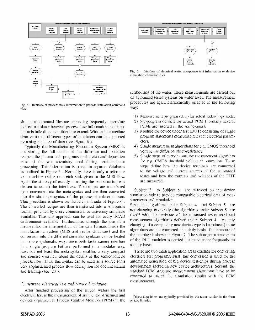
Fig. 6. Interface of process flow information to process simulation commandfiles
simulator command files are happening frequently. Thereforea direct translator between process flow information and simu-lation is inflexible and difficult to extend. With an intermediateabstract format different types of simulators can be supportedby a single source of data (see Figure 6 ).
Typically the Manufacturing Execution System (MES) isnot storing the full details of the diffusion and oxidationrecipes, the plasma etch programs or the etch and depositionrates of the wet chemistry used during semiconductorprocessing. This information is stored in separate databasesas outlined in Figure 6 . Normally there is only a referenceto a machine recipe or a etch sink given in the MES flow.Again the strategy of exactly mirroring the real situation waschosen to set up the interfaces. The recipes are transferredby a converter into the meta-syntax and are then convertedinto the simulator syntax of the process simulator chosen.This procedure is shown on the left hand side of Figure 6 .
The converted recipes are then transferred into a subroutineformat, provided by every commercial or university simulatoravailable. Thus this approach can be used for every TCADenvironment available. Furthermore, through the use of ameta-syntax the interpretation of the data formats inside themanufacturing system (MES and recipe databases) and theconversion into the different simulator syntaxes can be treatedin a more systematic way, since both tasks cannot interferein a single program but are performed in a modular way.Last but not least the meta-syntax enables a very compactand concise overview about the details of the semiconductorprocess flow. Thus, this syntax can be used as a source for avery sophisticated process flow description for documentationand training (see [20]).
C. Between Electrical Test and Device SimulationAfter finished processing of the silicon wafers the first
electrical test is the measurement of simple test structures anddevices organized in Process Control Monitors (PCM) in the
Fg.7Itf Eof electrical Wafer tcceptanbeVtest io on dc
s ES-lines Toch. wae PCMD.ThTe Measurement are Tcarre o
onEautomted tete sytm on wafe leel Th mesrmn
2) N.62 Progra. Subprogram d Sfbpogract P A (gorith m Allgrithm ra
PCMDaraae inDtbserte inDthbae scritbe-lieDtbs). aabs
3) Module for deviceunder~testc(DT conSisultigof singl
S4ihmslor e Ag.orith resol5)CSlfdfille mea Sur brontin al g r
Fig. 7. Interface of electrical wafer acceptance test information to devicesimulation command files
scribe-lines of the wafer. These measurements are carried outon automated tester systems on wafer level. The measurementprocedures are again hierarchically oriented in the followingway:
1) Measurement program set up for actual technology node.2) Subprogram defined for actual PCM (normally several
PCMs are inserted in the scribe-lines).3) Module for device under test (DUT) consisting of single
program statements measuring relevant electrical param-eters.
4) Single measurement algorithms for e.g. CMOS thresholdvoltage, or diffusion sheet-resistance.
5) Single steps of carrying out the measurement algorithmfor e.g. CMOS threshold voltage in saturation. Thesesteps define how the device terminals are connectedto the voltage and current sources of the automatedtester and how the currents and voltages of the DUTare measured.
Subject 3 to Subject 5 are mirrored on the devicesimulation side to provide comparable electrical data of mea-surements and simulation.Since the algorithms under Subject 4 and Subject 5 arenot changing frequently (the algorithms under Subject 5 arefixed with the hardware of the automated tester used andmeasurement algorithms defined under Subject 4 are onlychanging, if a completely new device type is introduced) thesealgorithms are not converted on a daily basis. The structure ofthe interface is shown in Figure 7 . The subprogram conversionof the DUT modules is carried out much more frequently ona daily basis.
There are two main application areas existing for convertingelectrical test programs. First, this conversion is used for theautomated generation of big device test-chips during processdevelopment including new device architectures. Second, thestandard PCM structure measurement algorithms have to beconverted to match the simulation results with the PCMmeasurements.
2these algorithms are typically provided by the tester vendor in the form
1-4244-0404-5/06/$20.00 © 2006 IEEE
S.-OhIld6fidUktht ftbOidAtlbh DtbAr.,. EiNglibbihiMt
MES-Sy.t..D.t.b.s. Diff..i." I.p ..t W.t- Eft h,.t. & Dy-Et,:h
F.,,,.,:. R.rip.s R.,:ip.r, D.p.riti..r.t. R.rip.sD.t.b.s. D.t.b.s. D.t.b.s. D.tb.s. D.t.b.s.
IF IF
r I'll ,,, r
M.t.s "t.. M.tsy"t.. M.tsy"t.. m.t.sy.t.. m.tsy"t..y S.bpr.gr.. S.bpr.gr.. S.bpr.gr.. S.bpr.gr..(ASCII) (ASCII) (ASCII) (ASCII) (ASCII)
c
Pr.c.sr,Si..I.t.r
A F
r.c.r,s A.t...tdSi..I.t.r R.cip. ..d Tr.i.i.g
B D.c....t.ti.,,r.c.s
Si ..I.t.r
c
SISPAD 2006 13
D. Between Device Characterization and Device Modeling(SPICE)
This interface deals with the generation of reliable devicemodels for circuit modeling (e.g. SPICE). The main devices(NMOS/PMOS transistors for standard CMOS processes and,in addition, bipolar transistors for BiCMOS processes) of anynew process fabrication must be characterized completely interms of output characteristics, transfer characteristics, ampli-fication, etc. This task results in scalable electrical models(BSIM3 for CMOS, VBIC for Bipolar transistors) or com-pact models for circuit simulation. In the TCAD fabricationintegration scheme the source for this fitting procedure canbe twofold: First, the usual way of measuring the charac-teristics on semiconductor wafer material and second, bysimulating these characteristics with device simulation. Thesecond approach has the enormous advantage of getting worstcase predictions [21], [22], which are directly related toprocess parameter changes by applying statistical variations onselected semiconductor process step parameters (e.g. selectedimplantation doses). Furthermore, combined process and de-vice simulations without the existence of any semiconductormaterial can generate preliminary models very early in theprocess development stage. Unfortunately the generation ofSPICE models (e.g. BSIM3.3 or BSIM4 with hundreds offree parameters) is not an automated straightforward task.The process characterization engineers have to set up manyinitial values for starting the optimization of actual SPICEmodels and have to follow a complicated iterative strategyto get a good model with reasonable accuracy. Thereforean automated global optimizer for generating a good SPICEmodel is not available. Currently the only way to get socalled "TCAD based models" is to generate characteristicswith device simulation as they were measured on a realdevice and submit this information to process characterizationengineers for the generation of SPICE models. Nevertheless,this approach enables the generation of a design environmentof a new technology in a very early stage of a processdevelopment. The time to market for new process technologiesis thus significantly reduced.
E. Package Modeling InterfaceSince package modeling does not have a key focus in
this work, the corresponding interface is not discussed indetail. However it would be beneficial to implement such aconversion into the overall TCAD flow. Since commercialpackage simulators provide a compact model (sub-circuit) ofthe parasitic elements introduced by the package, especiallyfor RF and power applications this additional input could bevery helpful. Currently this conversion is performed by handor, more typically, not considered at all in the design process.
V. USING TCAD WITH SPCA. IntroductionA semiconductor fabrication process consists of several
hundred unit process steps, each of which is subject topotential misprocessing. Such misprocessing typically occurs
when wrong tool recipes are loaded and executed, or processsteps are accidentally left out or performed twice. Althoughmany of these issues are immediately detected at the nextprocess step because of the physical deviation of the wafersfrom their usual appearance, some of these misprocessedwafers make their way through the whole production lineand the failure is only detected at electrical parameter test.In such cases it is paramount that the cause of the failure isidentified as quickly as possible to prevent other wafers inthe fabrication line from being misprocessed the same way.One special group of unit processes that is of particularinterest in this context is the group of implant steps.Advanced semiconductor process flows contain severaldozens of different implant steps, and since the implants doonly affect the electrical, but not the mechanical or opticalproperties of the semiconductor wafers, a missing or doubleimplant will typically be detected only at electrical test.Although large efforts have been made to prevent implantaccidents, a certain risk remains in every not fully automatedsemiconductor fabrication facility.Unfortunately, the relationship between the implantsperformed and the electrical behavior of the semiconductordevices is of high complexity, and the inference from theelectrical data obtained at test to what actually happenedduring production requires the judgment and experience fromdevice engineering experts.In the following an approach is shown, how this inferencecan be made by a broader range of personnel with an evenhigher level of certainty.During recent years, simulation techniques for semiconductorprocessing have been developed at a breathtaking speed. Itis therefore feasible today, to feed a process flow, includingall relevant process parameters, into a TCAD simulation,thereby creating a virtual semiconductor device such as atypical transistor, and extract the electrical properties of thissimulated device. Parameters such as thresholds, saturationcurrents, sheet resistances or similar can thus be calculatedfor almost any given process flow.So far, TCAD simulation has been extensively used forprocess development, but its application for manufacturingcontrol and corrective action was very limited, which ispartly due to the fact that its application needs skilledspecialists. The advantages, of running a complete set ofTCAD simulations of a transistor device for the process ofrecord (POR), and for all process flows that result from both,an accidental missing and double implant (for each implantstep), are described in the following.
B. Computational EffortThe current work is based on the analysis of austriami-
crosystems' 0.35,um CMOS-mixed-signal process licensedfrom TSMC. This industry standard process offers two dif-ferent gate oxide options (3.3V and 5V) resulting in 4 basicCMOS devices.Performing a full factorial simulation of only 3 parameters
1-4244-0404-5/06/$20.00 © 2006 IEEESISPAD 2006 14
(p-well, n-well and PMOS threshold adjust implant) withparameter values 0,1,2 (corresponding missing, correct anddouble implants) takes 33 = 27 different simulation runs.Because of speed and memory constraints only one CMOS-transistor can be simulated per run, 108 different runs haveto be executed to get the full information for these threeimplants on four transistors. This took a full weekend ona cluster of four 2GHz Linux computers, but having thesedata calculated up front, enables an engineer to identify veryquickly the step where misprocessing occurred, in case a lotfails at electrical parameter test. Furthermore, this informationhas to be calculated only once, since these data reflect thesituation in a frozen process flow.
C. Selecting a Set of ParametersSince this 0.35,um process contains 16 implants in total, it
is obvious that a full factorial computation is not feasible asthe number 4096 of required simulation runs for a full factorialdesign exceeds all reasonable computation efforts.However, it is neither necessary nor sensible to do a full fac-torial design, because, as the probability for a process incidentis rather small, the probability that multiple implant steps havebeen misprocessed is vanishing. However, it is not sufficientto calculate only the 32 situations for each single implantstep being skipped or doubly processed, because scenarioswhere a wrong implant recipe is used lead to situations whereone implant is missing and another one doubled. Hence, thepossible combinations of missed and double implants have tobe selected carefully. So, as can be seen from Table I , outof the possible 27 combinations only 1 (process of record) +3 times 2 (missing and double implant each) + 2 (swappedP- and N-Well implants) = 9 combinations remain that makesense.Furthermore, one can distinguish between different implant"classes" which affect only certain electrical parameters. E.g.,incidents related to the standard polysilicon resistor implant(poly 2 implant) can be easily detected by measurement of thepolysilicon resistance. Hence, only three TCAD calculationsneed to be performed to cover possible incidents at thisparticular implant step.This leads to the general requirement that some efforts areneeded to identify an appropriate set of electrical parameterswhich will give an unambiguous indication of the "culprit"implant.
D. Simulation ResultsThe parameter values were extracted from combined
process- and device simulations with the Synopsys softwaresuite. Each step of the process flow relevant for the devicestructures was taken into account for the process simulation.A device simulation of the NMOS and PMOS transistor typeswas performed to obtain device characteristics like saturationcurrent or NMOS threshold. The identical parameter extractionalgorithms as in actual electrical tests were applied to enablea comparison to measured values for calibration of the simu-lation. Finally, the relative deviation of the nominal electrical
parameters was calculated the results of which are shown inTable I . These results show clearly the power of the proposedmethod for identifying root causes for wafer misprocessing.By choosing the driving capability and the threshold voltageof two different types of NMOS and the driving capabilityof two different types of PMOS transistors an unabigous setof electrical parameters was obtained. The percentage valuesin the table are relative changes of the parameters comparedto the typical situation indicated in the first line of the table.Before the implementation of this method, it took valuabletime of PCM data analysis by an experienced device engineerto find switched PLDD and NLDD reticles as the root causefor a misprocessed lot.As these kinds of implant misprocessing incidents are rare,the system has to be understood as a preventive method toreact to such problems as quickly as possible. It can save both,expensive engineering resources and additional measurements.Furthermore, the system can be used to rule out a number ofspeculations by simply trying them out with simulation andcompare the "fingerprint" of their results.
VI. CONCLUSIONS AND OUTLOOK
Implementing a framework for the integration of TCADwith the actual fabrication process results in multiple impactson the strategic position of TCAD in a semiconductor fabri-cation environment.Historically TCAD was only applied on single device struc-tures and only during process development to gain betterinsight into the physics behind devices [23]. Additionally,information on physical quantities which are difficult to obtainexperimentally was gained. By automated integration of theTCAD framework over the whole work flow of semiconductorcircuit fabrication many additional application fields can beaddressed, as shown by this work. The setup of new pro-cesses (or the transfer of existing technologies) is speededup dramatically. The human induced errors are consecutelyreduced. The number of, at least passive, users of TCAD ina semiconductor company grows from a handful engineersto the entire engineering and production team. This resultsalso in a much better utilization of the resources spent inTCAD (software license costs, work efficiency of TCADengineers, computer hardware etc.). The gap in technicalinformation between the top management and the "engineer inthe production line" is made smaller. This aspect should not beunderestimated in the field of semiconductor industry becausedue to the high complexity of integrated circuit fabrication, anyclosed documentation of the processes is of inevitable value.However some open questions remain. The integration ofetching and deposition recipies via automatic conversion isstill on the level of transferring etch and deposition rates.The lack of generic equipment simulators for etching anddeposition leads to additional effort in calibrating these stepsin the TCAD simulation. Furthermore, there is still no fullyautomated approach to generate SPICE models from measure-ment or simulation data without user interaction. This leads toa significant amount of resource allocation at every additional
1-4244-0404-5/06/$20.00 © 2006 IEEESISPAD 2006 15
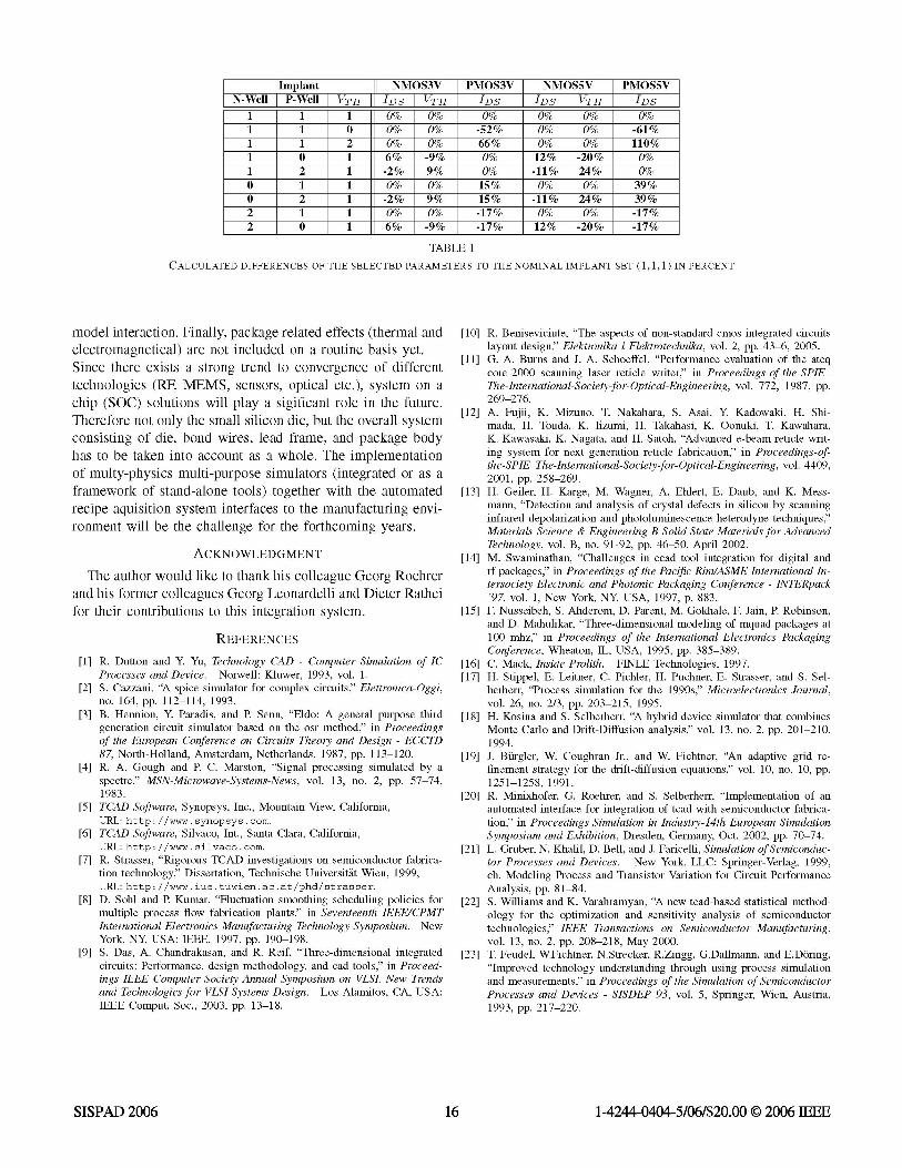
l Implant T|NMOS3V |PMOS3V | NMOS5V TPMOS5VlN-Well P-Well] VTH I IDS [ VTH IDS ID?S f VTH { IDS
1 1 1 0% 0% 0% 0% 0% 0%1 1 0 0% 0% -52% 0% 0% -61%1 1 2 0% 0% 66% 0% 0% 110%1 0 1 6% -9% 0% 12% -20% 0%1 2 1 -2% 9% 0% -11% 24% 0%0 1 1 0% 0% 15% 0% 0% 39%0 2 1 -2% 9% 15% -11% 24% 39%2 1 1 0% 0% -17% 0% 0% -17%2 0 1 6% -9% -17% 12% -20% -17%
TABLE ICALCULATED DIFFERENCES OF THE SELECTED PARAMETERS TO THE NOMINAL IMPLANT SET (1,1,1) IN PERCENT
model interaction. Finally, package related effects (thermal andelectromagnetical) are not included on a routine basis yet.Since there exists a strong trend to convergence of differenttechnologies (RF, MEMS, sensors, optical etc.), system on achip (SOC) solutions will play a sigificant role in the future.Therefore not only the small silicon die, but the overall systemconsisting of die, bond wires, lead frame, and package bodyhas to be taken into account as a whole. The implementationof multy-physics multi-purpose simulators (integrated or as aframework of stand-alone tools) together with the automatedrecipe aquisition system interfaces to the manufacturing envi-ronment will be the challenge for the forthcoming years.
ACKNOWLEDGMENT
The author would like to thank his colleague Georg Roehrerand his former colleagues Georg Leonardelli and Dieter Ratheifor their contributions to this integration system.
REFERENCES
[1] R. Dutton and Y Yu, Technology CAD - Computer Simulation of ICProcesses and Device. Norwell: Kluwer, 1993, vol. 1.
[2] S. Cazzani, "A spice simulator for complex circuits," Elettronica-Oggi,no. 164, pp. 112-114, 1993.
[3] B. Hennion, Y Paradis, and P. Senn, "Eldo: A general purpose thirdgeneration circuit simulator based on the osr method," in Proceedingsof the European Conference on Circuits Theory and Design - ECCTD87, North-Holland, Amsterdam, Netherlands, 1987, pp. 113-120.
[4] R. A. Gough and P. C. Marston, "Signal processing simulated by aspectre," MSN-Microwave-Systems-News, vol. 13, no. 2, pp. 57-74,1983.
[5] TCAD Software, Synopsys, Inc., Mountain View, California,URL:http://www.synopsys.com.
[6] TCAD Software, Silvaco, Int., Santa Clara, California,URL:http://www.silvaco.com.
[7] R. Strasser, "Rigorous TCAD investigations on semiconductor fabrica-tion technology," Dissertation, Technische Universitat Wien, 1999,URL:http://www.iue.tuwien.ac.at/phd/strasser.
[8] D. Sohl and P. Kumar, "Fluctuation smoothing scheduling policies formultiple process flow fabrication plants," in Seventeenth IEEE/CPMTInternational Electronics Manufacturing Technology Symposium. NewYork, NY, USA: IEEE, 1997, pp. 190-198.
[9] S. Das, A. Chandrakasan, and R. Reif, "Three-dimensional integratedcircuits: Performance, design methodology, and cad tools," in Proceed-ings IEEE Computer Society Annual Symposium on VLSI. New Trendsand Technologies for VLSI Systems Design. Los Alamitos, CA, USA:IEEE Comput. Soc., 2003, pp. 13-18.
[10] R. Beniseviciute, "The aspects of non-standard cmos integrated circuitslayout design," Elektronika i Elektrotechnika, vol. 2, pp. 43-6, 2005.
[11] G. A. Burns and J. A. Schoeffel, "Performance evaluation of the ateqcore-2000 scanning laser reticle writer," in Proceedings-of-the-SPIE-The-International-Society-for-Optical-Engineering, vol. 772, 1987, pp.269-276.
[12] A. Fujii, K. Mizuno, T. Nakahara, S. Asai, Y Kadowaki, H. Shi-mada, H. Touda, K. lizumi, H. Takahasi, K. Oonuki, T. Kawahara,K. Kawasaki, K. Nagata, and H. Satoh, "Advanced e-beam reticle writ-ing system for next generation reticle fabrication," in Proceedings-of-the-SPIE-The-International-Society-for-Optical-Engineering, vol. 4409,2001, pp. 258-269.
[13] H. Geiler, H. Karge, M. Wagner, A. Ehlert, E. Daub, and K. Mess-mann, "Detection and analysis of crystal defects in silicon by scanninginfrared depolarization and photoluminescence heterodyne techniques,"Materials Science & Engineering B Solid State Materials for AdvancedTechnology, vol. B, no. 91-92, pp. 46-50, April 2002.
[14] M. Swaminathan, "Challenges in ecad tool integration for digital andrf packages," in Proceedings of the Pacific Rim/ASME International In-tersociety Electronic and Photonic Packaging Conference - INTERpack'97, vol. 1, New York, NY, USA, 1997, p. 883.
[15] F. Nusseibeh, S. Ahderom, D. Parent, M. Gokhale, F. Jain, P. Robinson,and D. Mahulikar, "Three-dimensional modeling of mquad packages at100 mhz," in Proceedings of the International Electronics PackagingConference, Wheaton, IL, USA, 1995, pp. 385-389.
[16] C. Mack, Inside Prolith. FINLE Technologies, 1997.[17] H. Stippel, E. Leitner, C. Pichler, H. Puchner, E. Strasser, and S. Sel-
berherr, "Process simulation for the 1990s," Microelectronics Journal,vol. 26, no. 2/3, pp. 203-215, 1995.
[18] H. Kosina and S. Selberherr, "A hybrid device simulator that combinesMonte Carlo and Drift-Diffusion analysis," vol. 13, no. 2, pp. 201-210,1994.
[19] J. Biirgler, W. Coughran Jr., and W. Fichtner, "An adaptive grid re-finement strategy for the drift-diffusion equations," vol. 10, no. 10, pp.1251-1258, 1991.
[20] R. Minixhofer, G. Roehrer, and S. Selberherr, "Implementation of anautomated interface for integration of tcad with semiconductor fabrica-tion," in Proceedings Simulation in Industry-14th European SimulationSymposium and Exhibition, Dresden, Germany, Oct. 2002, pp. 70-74.
[21] L. Gruber, N. Khalil, D. Bell, and J. Faricelli, Simulation ofSemiconduc-tor Processes and Devices. New York, LLC: Springer-Verlag, 1999,ch. Modeling Process and Transistor Variation for Circuit PerformanceAnalysis, pp. 81-84.
[22] S. Williams and K. Varahramyan, "A new tcad-based statistical method-ology for the optimization and sensitivity analysis of semiconductortechnologies," IEEE Transactions on Semiconductor Manufacturing,vol. 13, no. 2, pp. 208-218, May 2000.
[23] T. Feudel, W.Fichtner, N.Strecker, R.Zingg, G.Dallmann, and E.Doring,"Improved technology understanding through using process simulationand measurements," in Proceedings of the Simulation of SemiconductorProcesses and Devices - SISDEP 93, vol. 5, Springer, Wien, Austria,1993, pp. 217-220.
1-4244-0404-5/06/$20.00 © 2006 IEEESISPAD 2006 16