Embed Size (px)
Citation preview
Development of 6.1 A Materials for IR Applications
(Second-year Report)
by Gregory Brill and Yuanping Chen
ARL-TR-5855 December 2011
Approved for public release; distribution unlimited.
NOTICES
Disclaimers
The findings in this report are not to be construed as an official Department of the Army position
unless so designated by other authorized documents.
Citation of manufacturer’s or trade names does not constitute an official endorsement or
approval of the use thereof.
Destroy this report when it is no longer needed. Do not return it to the originator.
Army Research Laboratory Adelphi, MD 20783-1197
ARL-TR-5855 December 2011
Development of 6.1 A Materials for IR Applications
(Second-year Report)
Gregory Brill and Yuanping Chen
Sensors and Electron Devices Directorate, ARL
Approved for public release; distribution unlimited.

ii
REPORT DOCUMENTATION PAGE Form Approved
OMB No. 0704-0188 Public reporting burden for this collection of information is estimated to average 1 hour per response, including the time for reviewing instructions, searching existing data sources, gathering and maintaining the
data needed, and completing and reviewing the collection information. Send comments regarding this burden estimate or any other aspect of this collection of information, including suggestions for reducing the
burden, to Department of Defense, Washington Headquarters Services, Directorate for Information Operations and Reports (0704-0188), 1215 Jefferson Davis Highway, Suite 1204, Arlington, VA 22202-4302.
Respondents should be aware that notwithstanding any other provision of law, no person shall be subject to any penalty for failing to comply with a collection of information if it does not display a currently
valid OMB control number.
PLEASE DO NOT RETURN YOUR FORM TO THE ABOVE ADDRESS.
1. REPORT DATE (DD-MM-YYYY)
December 2011
2. REPORT TYPE
DRI
3. DATES COVERED (From - To)
4. TITLE AND SUBTITLE
Development of 6.1 A Materials for IR Applications (Second-year Report)
5a. CONTRACT NUMBER
5b. GRANT NUMBER
5c. PROGRAM ELEMENT NUMBER
6. AUTHOR(S)
Gregory Brill and Yuanping Chen
5d. PROJECT NUMBER
5e. TASK NUMBER
5f. WORK UNIT NUMBER
7. PERFORMING ORGANIZATION NAME(S) AND ADDRESS(ES)
U.S. Army Research Laboratory
ATTN: RDRL-SE
2800 Powder Mill Road
Adelphi, MD 20783-1197
8. PERFORMING ORGANIZATION REPORT NUMBER
ARL-TR-5855
9. SPONSORING/MONITORING AGENCY NAME(S) AND ADDRESS(ES)
10. SPONSOR/MONITOR'S ACRONYM(S)
11. SPONSOR/MONITOR'S REPORT NUMBER(S)
12. DISTRIBUTION/AVAILABILITY STATEMENT
Approved for public release; distribution unlimited.
13. SUPPLEMENTARY NOTES
14. ABSTRACT
The development of mercury cadmium selenide (HgCdSe) material for infrared (IR) applications was initiated in fiscal year
2010 (FY10) at the U.S. Army Research Laboratory (ARL) under a Director’s Research Initiative (DRI) program. Material
growth conditions using molecular beam epitaxy (MBE) were identified to achieve reasonably good material quality in terms
of surface morphology, defect density, and crystallinity as measured by x-ray diffraction. Additionally, it was determined that
the bandgap of HgCdSe could be tuned by controlling the selenium (Se) to cadmium (Cd) flux ratio during growth. This
research has continued in fiscal year 2011 (FY11) with an emphasis placed on developing composite substrate technology
(zinc telluride [ZnTe]/silicon [Si] and Zn(Se)Te/gallium antimonide [GaSb]) for HgCdSe as well as understanding the
electrical properties of HgCdSe material. An etching process was developed to identify dislocations in HgCdSe. Finally, the
continued study of MBE growth parameters and their impact on material properties was conducted.
15. SUBJECT TERMS
HgCdSe, ZnTe, MBE, IR, GaSb
16. SECURITY CLASSIFICATION OF: 17. LIMITATION
OF ABSTRACT
UU
18. NUMBER OF
PAGES
26
19a. NAME OF RESPONSIBLE PERSON
Gregory Brill
a. REPORT
Unclassified
b. ABSTRACT
Unclassified
c. THIS PAGE
Unclassified
19b. TELEPHONE NUMBER (Include area code)
(301) 394-0192
Standard Form 298 (Rev. 8/98)
Prescribed by ANSI Std. Z39.18
iii
Contents
List of Figures iv
Acknowledgments v
1. Objective 1
2. Background 1
3. Approach 2
3.1 Teaming ...........................................................................................................................2
3.2 Research Plan ..................................................................................................................3
4. Results 3
4.1. Development of Composite Substrates for HgCdSe .......................................................3
4.1.1 MBE Growth of ZnTe/Si .....................................................................................3
4.1.2 MBE Growth of Zn(Se)Te/GaSb ........................................................................6
4.2 Etch Pit Density (EPD) Measurements of HgCdSe ........................................................6
4.3 HgCdSe Structural Characterization ...............................................................................8
4.4 HgCdSe Electrical Characterization ..............................................................................10
5. References 13
6. Transitions 14
List of Symbols, Abbreviations, Acronyms 15
Distribution List 17
iv
List of Figures
Figure 1. Energy Gap vs. lattice parameter for several semiconductor material systems. .............2
Figure 2. X-ray FWHM (right axis) and EPD measurements (left axis) of ZnTe/Si(211) films under different Zn/Te fluxes. ............................................................................................5
Figure 3. Surface morphology of ZnTe/Si(211) films under different Zn/Te fluxes. .....................5
Figure 4. HgCdSe surface before (left) and after (right) etching in a solution designed to reveal the presence of dislocations. ...........................................................................................7
Figure 5. Etch rate of the EPD etch for HgCdSe material being developed at ARL. .....................8
Figure 6. Surface images from two HgCdSe layers. Each was grown under identical conditions except for an increase in Hg flux. ............................................................................9
Figure 7. TEM images and optical microscopy images of HgCdSe grown on ZnTe/Si substrates under various growth temperature and flux ratios. .................................................10
v
Acknowledgments
We wish to acknowledge the efforts of Mr. Kevin Doyle and Prof. Thomas Myers from Texas
State University for assistance with HgCdSe growth and electrical characterization.
Additionally, we would like to thank Dr. Sudhir Trivedi of Brimrose Corporation for his
assistance with etchant chemistry research.
vi
INTENTIONALLY LEFT BLANK.
1
1. Objective
This project is a continuation of research that began in fiscal year 2010 (FY10) on the
development of mercury cadmium selenide (HgCdSe) material for infrared (IR) applications. At
the time, virtually no information existed regarding HgCdSe material growth on nearly lattice-
matched zinc telluride (ZnTe)/silicon (Si) or gallium antimonide (GaSb) substrates using
molecular beam epitaxy (MBE). Reasonably good material quality in terms of surface
morphology, defect density, and crystallinity as measured by x-ray diffraction was obtained
during the first year of this program. Additionally, it was determined that the bandgap of
HgCdSe could be tuned by controlling the selenium (Se) to cadmium (Cd) flux ratio during
growth (1). Based on these promising initial results, further studies were warranted and carried
out.
2. Background
Currently, mercury cadmium telluride (HgCdTe) is the material used in the majority of fielded
Army IR systems and much effort has been expended to push the technology to both large-
format and low-cost systems while still maintaining superior performance. However, this
technology has been limited in its application due to the size and cost constraints related to its
substrate, bulk grown cadmium zinc telluride (CdZnTe). One potential solution is to use large
area Si substrates for the growth of HgCdTe. However, due to the huge lattice mismatch
between Si and HgCdTe (19%) and the associated strain energy, misfit dislocations need to be
generated somewhere in the thin-film stack to alleviate this energy, which ultimately propagates
into the IR absorbing layer. Generally, a two orders of magnitude higher dislocation density is
present in scalable HgCdTe/Si material with respect to non-scalable HgCdTe/CdZnTe. It has
been demonstrated that this higher dislocation level results in lower device performance (2).
Figure 1 shows the lattice constant and bandgap of various semiconductor systems. As shown in
the figure, numerous materials have lattice constants at or near 0.61 nm, including mercury
selenide (HgSe) (a semimetal) and cadmium selenide (CdSe) (a wide bandgap semiconductor).
By forming an alloy of Hg1–xCdxSe, the bandgap of the material can be tuned to absorb any
wavelength of IR light, resulting in an ideal material to cover the entire IR spectral range. This
system is completely analogous to mercury telluride (HgTe) and cadmium telluride (CdTe)
binary semiconductors with the significant advantage being that two III-V binary semiconductors
are available to use as substrates for HgCdSe, specifically indium arsenide (InAs) and GaSb.
These substrates are scalable and readily available from commercial suppliers within the United
States, in stark contrast to CdZnTe substrates. By using III-V bulk substrates, a starting template
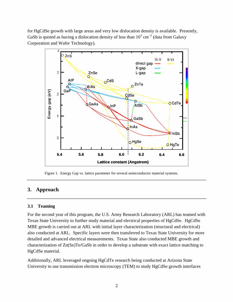
2
for HgCdSe growth with large areas and very low dislocation density is available. Presently,
GaSb is quoted as having a dislocation density of less than 103 cm
–2 (data from Galaxy
Corporation and Wafer Technology).
5.4 5.85.6 6.26.0 6.66.4
Lattice constant (Angstrom)
5.4 5.85.6 6.26.0 6.66.4
Lattice constant (Angstrom)
Figure 1. Energy Gap vs. lattice parameter for several semiconductor material systems.
3. Approach
3.1 Teaming
For the second year of this program, the U.S. Army Research Laboratory (ARL) has teamed with
Texas State University to further study material and electrical properties of HgCdSe. HgCdSe
MBE growth is carried out at ARL with initial layer characterization (structural and electrical)
also conducted at ARL. Specific layers were then transferred to Texas State University for more
detailed and advanced electrical measurements. Texas State also conducted MBE growth and
characterization of Zn(Se)Te/GaSb in order to develop a substrate with exact lattice matching to
HgCdSe material.
Additionally, ARL leveraged ongoing HgCdTe research being conducted at Arizona State
University to use transmission electron microscopy (TEM) to study HgCdSe growth interfaces
3
on different substrates as well as investigate material quality due to changes in growth
temperature. This work was conducted under an Army Research Office (ARO)-funded program
titled “Advanced Microstructural Characterization for Development of Improved HgCdTe.”
3.2 Research Plan
Three distinct areas of research were conducted related to this technology and are discussed in
this report.
Initially, minimal research time was devoted to the growth or preparation of the substrate
materials as the goal was to study the growth parameters and material characteristics related to
HgCdSe material. However, with the success achieved in the first year of the program, it was
determined that significant effort was warranted on developing composite substrate technology
specifically for HgCdSe. To this end, ARL conducted a systematic study of ZnTe/Si growth
with the goal of achieving smoother surface morphology material, with minimal defects and the
highest crystallinity, as determined by x-ray diffraction and etch pit studies of dislocation
density. As a corollary project, research was conducted on growing Zn(Se)Te on GaSb
substrates at Texas State University by MBE. By incorporating Se into the ZnTe matrix, exact
lattice matching between HgCdSe and the bulk grown GaSb substrate could be achieved.
The second area of research focused on the continued study of MBE growth parameters on the
structural quality of HgCdSe material. Constituent fluxes were varied as well as changes in the
growth temperature. Additionally, a significant effort was placed on developing a dislocation
revealing etch to ascertain the quality of material grown both on ZnTe/Si substrates as well as on
GaSb substrates. This was necessary as no etch existed that could reveal dislocations within
HgCdSe(211) material, a key metric for determining quality of material. Also, TEM studies
were carried out at Arizona State University under an existing ARO program with the goal of
understanding substrate preparation processes and epilayer nucleation processes.
Finally, the electrical properties of HgCdSe were investigated using Hall measurements at both
ARL and Texas State University.
4. Results
4.1. Development of Composite Substrates for HgCdSe
4.1.1 MBE Growth of ZnTe/Si
As shown in figure 1, ZnTe is nearly lattice matched to HgCdSe and was chosen as a substrate
for this program. This was done so that a baseline HgCdSe growth process could quickly be
achieved since ARL has extensive expertise in cleaning, preparing, and nucleating mercury (Hg)-
based compounds on II-VI based composite substrates. However, ZnTe material is generally
4
only grown as a buffer layer for CdTe/Si, and hence, little focus has ever been given to growing
thick ZnTe material as a substrate. As the need for high quality ZnTe/Si material became more
desirable, a systematic study on ZnTe nucleation and growth on Si(211) substrates was
conducted. The (211) orientation was chosen as this is the preferred orientation for the HgCdSe
material we have been developing (1). Besides, its potential use for HgCdSe material, high
quality ZnTe/Si can also be used for Type II superlattice materials, which are comprised of GaSb
and InAs, both with lattice parameters at or very near 0.61 nm (see figure 1).
To initiate ZnTe growth, migration enhanced epitaxy (MEE) was used after proper thermal
cleaning and passivation of the Si substrate was completed (4). The MEE process entails
opening the Te source for 10 s, followed by a null period of 10 s during which no material flux is
allowed to reach the substrate surface. Then the Zn source is opened for 10 s, again followed by
a null period of 10 s. This process is then repeated 66 times followed by a high temperature
annealing process under appropriate fluxes. Ultimately, the MEE process nucleates an
approximately 5-nm-thick ZnTe layer, which is of good crystal quality. This is the standard
process used for CdTe/Si composite substrate technology, an ARL-developed process used for
HgCdTe IR material growth. However, for HgCdSe, ZnTe/Si itself is the desired composite
substrate; hence, much thicker material is required.
For MBE growth, it is well established that growth temperature is one of the key parameters that
dictates the quality and morphology of the epilayer. Since ZnTe was grown using a two-step
process, both the nucleation temperature and growth temperature were optimized independently.
Additionally, the Zn/Te flux ratio used during growth was also a parameter of study. Multiple
ZnTe/Si layers were grown and analyzed using x-ray diffraction to measure overall crystallinity,
etch pit density (EPD) measurements of dislocation density using the Benson etch (3), and
optical microscopy observations of the surface morphology.
Results indicate that a temperature of 300 °C is optimal for both the nucleation of ZnTe using
MEE as well as the final growth temperature used when non-MEE (i.e., congruent deposition of
Zn and Te simultaneously) ZnTe is deposited. A significant increase in EPD was observed for a
higher nucleation temperature (340 °C) as well as a slight increase in the x-ray diffraction peak
full width at half maximum (FWHM), which indicates a more disordered/defective crystal
structure. Similar results were obtained when the growth temperature was decreased (260 °C) as
both the EPD values and x-ray FWHM values increased. Overall though, there is about a 20 °C
nucleation and growth temperature window in which high quality ZnTe/Si can be grown.
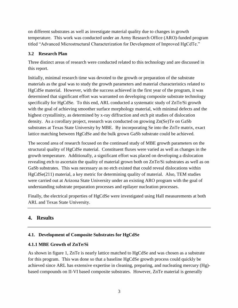
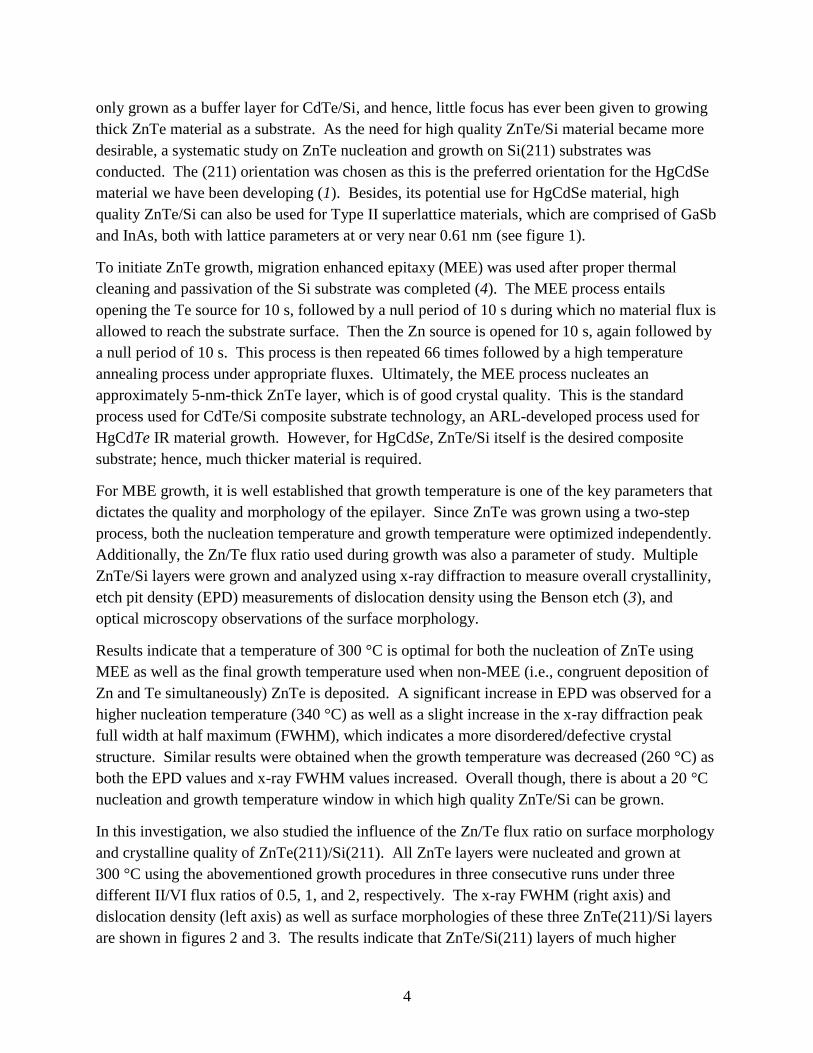
In this investigation, we also studied the influence of the Zn/Te flux ratio on surface morphology
and crystalline quality of ZnTe(211)/Si(211). All ZnTe layers were nucleated and grown at
300 °C using the abovementioned growth procedures in three consecutive runs under three
different II/VI flux ratios of 0.5, 1, and 2, respectively. The x-ray FWHM (right axis) and
dislocation density (left axis) as well as surface morphologies of these three ZnTe(211)/Si layers
are shown in figures 2 and 3. The results indicate that ZnTe/Si(211) layers of much higher
5
quality were obtained when grown under either Te-rich or equal Te and Zn fluxes. ZnTe(211)
layers grown under a Zn-rich environment, exhibit, without exception, a very hazy surface
morphology visible, even to the unaided eye, and a very broad x-ray FWHM, a factor of four
higher than that of the layers grown under Te-rich conditions.
Figure 2. X-ray FWHM (right axis) and EPD measurements (left axis) of ZnTe/Si(211)
films under different Zn/Te fluxes.
Figure 3. Surface morphology of ZnTe/Si(211) films under different Zn/Te fluxes.
This is an important result for developing high quality ZnTe/Si material for HgCdSe growth. It
also differs from our experience in growing CdTe/Si(211) and was not implemented during the
initial phase of this study (1). In the case of ZnTe, which is comprised of elements from row 3
(Zn) and row 4 (Te) of the Periodic Table, increased imbalance in the thermodynamic properties
of Zn and Te probably leads to increased sensitivity of surface morphology and crystalline
quality to the Zn/Te flux ratio. In contrast, for CdTe, both elements reside on row 4 of the
Periodic Table and have more similar thermodynamic properties. Hence, for CdTe, a 1:1 flux
ratio is easily obtained and is sufficient for high quality growth.
6
4.1.2 MBE Growth of Zn(Se)Te/GaSb
As ARL focused its efforts on improving ZnTe/Si as a composite substrate for HgCdSe, our
partners at Texas State University focused growing II-VI materials on GaSb substrates. Texas
State University has expertise with H cleaning of GaSb substrates, which makes for a more
reproducible cleaning process (5) as well as facilities that include a II-VI MBE growth chamber
interconnected through ultra high vacuum (UHV) to a III-V MBE growth chamber. Therefore,
they can properly clean large-area GaSb substrates, re-grow a GaSb buffer layer if so desired,
and then deposit a Zn(Se)Te thin film that is lattice matched to HgCdSe all without exposing the
sample to atmosphere. This is a capability ARL does not have as our II-VI and III-V MBE
growth chambers are isolated systems.
Recently, Texas State has demonstrated pseudomorphic growth of ZnTe on GaSb with a critical
thickness determined to be 350 nm. For ZnTe films kept below this thickness, very high quality
material was grown as determined by low temperature photoluminescence (PL) imaging, which
can indicate the presence of defect centers associated with dislocations. From these
measurements, ZnTe/GaSb material with a dislocation density estimated with an upper limit of
~1 x 105 cm
–2 was obtained (6). This result is very encouraging for this program as it indicates
that strained, defect-free ZnTe material can be deposited on large-area GaSb substrates. This is
the ideal substrate for subsequent HgCdSe growth. Furthermore, x-ray measurements have
confirmed that if Se is added to the ZnTe matrix, exact lattice matching to HgCdSe can be
achieved. With these two new developments, extremely low dislocation density HgCdSe grown
on large-area GaSb should be able to be achieved as the very small lattice mismatch between
HgCdSe and GaSb will be now accounted for, which otherwise could have led to an increase in
HgCdSe dislocation density.
4.2 Etch Pit Density (EPD) Measurements of HgCdSe
The key motivation for studying and developing HgCdSe materials is the desire to develop a
tunable IR material on a large-area scalable substrate with low dislocation density. For HgCdTe,
an industry etch has been in place for over 20 years that reveals dislocation within the material in
order to ascertain this important material quality characteristic. Recently, Benson et al. (3)
developed a new etch that improves the dislocation etching process and works equally well on
HgCdTe(211) and CdTe(211). However, when these etches were applied to HgCdSe(211) no
discernible etch pits were formed and the surface was more or less unaffected. By replacing Te
atoms with Se atoms, the chemistry of the etching process has been significantly altered. Under
this program, we have been developing the appropriate chemistry that can etch HgCdSe and
reveal the presence of dislocations.
Several possible etchants were selected by studying the literature related to ZnSe, CdSe, and
HgSe. Unfortunately, even in these binary semiconductor systems, no standard dislocation
revealing etchant exists. Through literature search, trial and error, and extensive discussions
with Dr. Sudhir Trivedi, a visiting scientist at ARL from Brimrose Corp with extensive
7
knowledge of chemistry related to materials science, we have come across a promising solution
that reveals etch pits that by all indications appear to be related to dislocations in HgCdSe.
Currently, no direct TEM evidence between an etch pit and an atomic dislocation has been
obtained, but this type of study is a focus of our ongoing work. Nonetheless, a pit revealing etch
is a first for this material system.
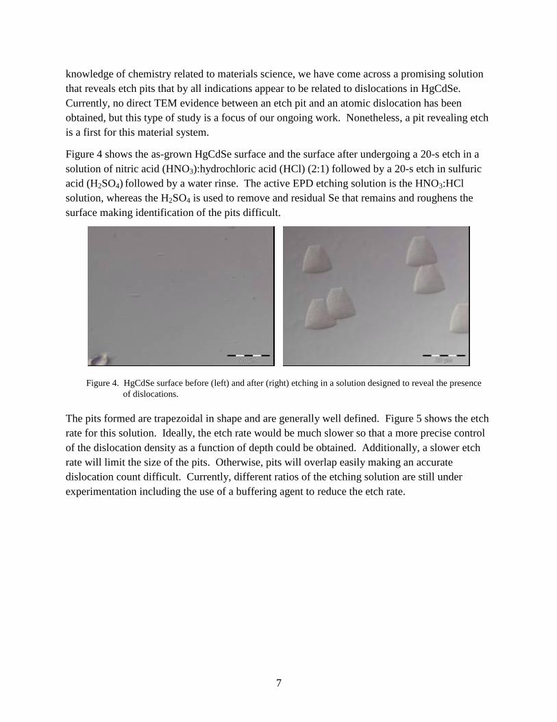
Figure 4 shows the as-grown HgCdSe surface and the surface after undergoing a 20-s etch in a
solution of nitric acid (HNO3):hydrochloric acid (HCl) (2:1) followed by a 20-s etch in sulfuric
acid (H2SO4) followed by a water rinse. The active EPD etching solution is the HNO3:HCl
solution, whereas the H2SO4 is used to remove and residual Se that remains and roughens the
surface making identification of the pits difficult.
Figure 4. HgCdSe surface before (left) and after (right) etching in a solution designed to reveal the presence
of dislocations.
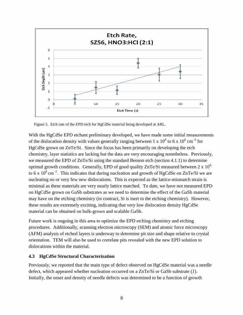
The pits formed are trapezoidal in shape and are generally well defined. Figure 5 shows the etch
rate for this solution. Ideally, the etch rate would be much slower so that a more precise control
of the dislocation density as a function of depth could be obtained. Additionally, a slower etch
rate will limit the size of the pits. Otherwise, pits will overlap easily making an accurate
dislocation count difficult. Currently, different ratios of the etching solution are still under
experimentation including the use of a buffering agent to reduce the etch rate.
8
Figure 5. Etch rate of the EPD etch for HgCdSe material being developed at ARL.
With the HgCdSe EPD etchant preliminary developed, we have made some initial measurements
of the dislocation density with values generally ranging between 1 x 10⁶ to 6 x 10
6 cm
–2 for
HgCdSe grown on ZnTe/Si. Since the focus has been primarily on developing the etch
chemistry, layer statistics are lacking but the data are very encouraging nonetheless. Previously,
we measured the EPD of ZnTe/Si using the standard Benson etch (section 4.1.1) to determine
optimal growth conditions. Generally, EPD of good quality ZnTe/Si measured between 2 x 10⁶
to 6 x 10⁶
cm–2
. This indicates that during nucleation and growth of HgCdSe on ZnTe/Si we are
nucleating no or very few new dislocations. This is expected as the lattice-mismatch strain is
minimal as these materials are very nearly lattice matched. To date, we have not measured EPD
on HgCdSe grown on GaSb substrates as we need to determine the effect of the GaSb material
may have on the etching chemistry (in contract, Si is inert to the etching chemistry). However,
these results are extremely exciting, indicating that very low dislocation density HgCdSe
material can be obtained on bulk-grown and scalable GaSb.
Future work is ongoing in this area to optimize the EPD etching chemistry and etching
procedures. Additionally, scanning electron microscopy (SEM) and atomic force microscopy
(AFM) analysis of etched layers is underway to determine pit size and shape relative to crystal
orientation. TEM will also be used to correlate pits revealed with the new EPD solution to
dislocations within the material.
4.3 HgCdSe Structural Characterization
Previously, we reported that the main type of defect observed on HgCdSe material was a needle
defect, which appeared whether nucleation occurred on a ZnTe/Si or GaSb substrate (1).
Initially, the onset and density of needle defects was determined to be a function of growth
9
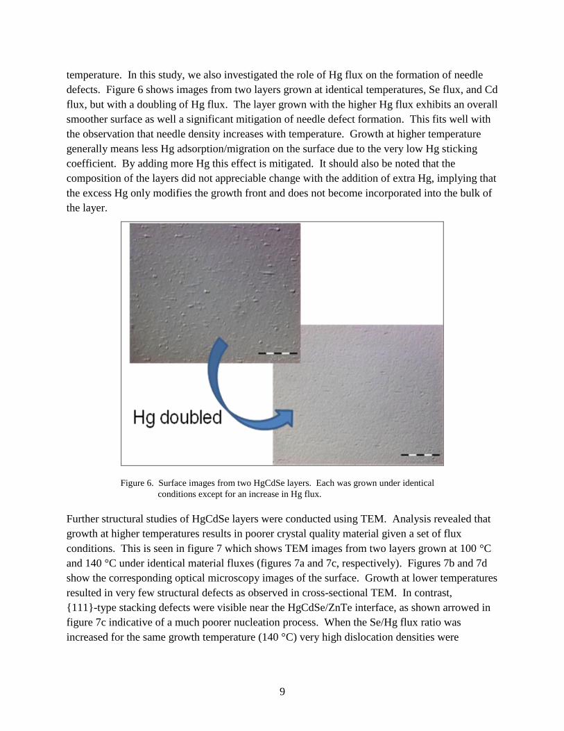
temperature. In this study, we also investigated the role of Hg flux on the formation of needle
defects. Figure 6 shows images from two layers grown at identical temperatures, Se flux, and Cd
flux, but with a doubling of Hg flux. The layer grown with the higher Hg flux exhibits an overall
smoother surface as well a significant mitigation of needle defect formation. This fits well with
the observation that needle density increases with temperature. Growth at higher temperature
generally means less Hg adsorption/migration on the surface due to the very low Hg sticking
coefficient. By adding more Hg this effect is mitigated. It should also be noted that the
composition of the layers did not appreciable change with the addition of extra Hg, implying that
the excess Hg only modifies the growth front and does not become incorporated into the bulk of
the layer.
Figure 6. Surface images from two HgCdSe layers. Each was grown under identical
conditions except for an increase in Hg flux.
Further structural studies of HgCdSe layers were conducted using TEM. Analysis revealed that
growth at higher temperatures results in poorer crystal quality material given a set of flux
conditions. This is seen in figure 7 which shows TEM images from two layers grown at 100 °C
and 140 °C under identical material fluxes (figures 7a and 7c, respectively). Figures 7b and 7d
show the corresponding optical microscopy images of the surface. Growth at lower temperatures
resulted in very few structural defects as observed in cross-sectional TEM. In contrast,
{111}-type stacking defects were visible near the HgCdSe/ZnTe interface, as shown arrowed in
figure 7c indicative of a much poorer nucleation process. When the Se/Hg flux ratio was
increased for the same growth temperature (140 °C) very high dislocation densities were
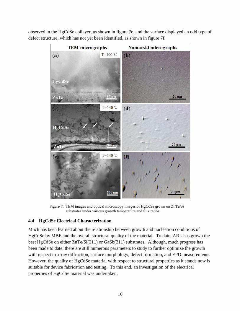
10
observed in the HgCdSe epilayer, as shown in figure 7e, and the surface displayed an odd type of
defect structure, which has not yet been identified, as shown in figure 7f.
Figure 7. TEM images and optical microscopy images of HgCdSe grown on ZnTe/Si
substrates under various growth temperature and flux ratios.
4.4 HgCdSe Electrical Characterization
Much has been learned about the relationship between growth and nucleation conditions of
HgCdSe by MBE and the overall structural quality of the material. To date, ARL has grown the
best HgCdSe on either ZnTe/Si(211) or GaSb(211) substrates. Although, much progress has
been made to date, there are still numerous parameters to study to further optimize the growth
with respect to x-ray diffraction, surface morphology, defect formation, and EPD measurements.
However, the quality of HgCdSe material with respect to structural properties as it stands now is
suitable for device fabrication and testing. To this end, an investigation of the electrical
properties of HgCdSe material was undertaken.
11
Simple Van der Pauw Hall measurements (300 and 77 K) were conducted at ARL while Texas
State performed quantitative mobility spectrum analysis (QMSA) on selected samples using
variable magnetic fields over a wide range of temperatures (300 to 4 K). Additionally, several
annealing experiments were carried out to study the overall electrical performance of the
material.
Results at ARL indicated high intrinsic n-type doping (carrier concentrations measuring 1 x
1017
cm–3
or greater) of as-grown material if grown intentionally undoped. This result differs
considerable from intentionally undoped HgCdTe material in which as-grown material can be p-
type due to the presence of Hg vacancies. As this high value of n-type intrinsic carrier
concentration is not desirable for devices, several annealing experiments were conducted.
Annealing under either a vacuum environment or a Se environment at 250 °C for 24 h did not
significantly alter the intrinsic carrier concentration. However, the mobility of the material did
generally improve after such anneals by approximately a factor two. In contrast, annealing under
a Hg environment lead to an order of magnitude increase in carrier concentration. Initially, this
effect was attributed to Hg interstitials being formed within the crystal, which can act as double
ionized donors (7). However, this result was only temporary. If the same sample was measured
months later, the carrier concentration would be back to the as-grown levels. At this time, it is
uncertain if annealing under Hg creates a temporary surface state, which alters the electrical
activity, or if some other factor is involved.
Further Hall studies were conducted at Texas State University, which has the capability to cool
the samples to 4 K as well as measure Hall under various magnetic fields. QMSA analysis
indicated the presence of at least two n-type carries in most samples. At this time, it is unclear as
to the origin of each carrier type, although it is assumed that the interface may be contributing as
well as the bulk of the material. Also, one of the carrier types displayed a broad mobility
spectrum indicative of the nonhomogeneity of the sample. Neither of these results is particularly
surprising as the samples studied were grown prior to optimization of the ZnTe/Si substrate
material or the nucleation process. More important was the finding that the carrier concentration
of intentionally undoped HgCdSe material remained relatively flat from 4 to 300 K. This
indicates that the behavior observed is most likely intrinsic to the material and a function of
growth conditions. With this information, we are revisiting our growth process. Specifically, we
were growing HgCdSe using a standard Se source, which is known to produce Se6 molecules. It
is speculated that the Se6 is hard to incorporate into the growing film, especially given the low
growth temperatures needed to obtain good material quality (100 °C). This is also different to
HgCdTe film growth in which a standard MBE Te source produces Te2. If Se6 is not being fully
incorporated, we are in essence growing HgCdSe with a high number of Se vacancies, which can
act as n-type dopants. To test this hypothesis, we will start “cracking” Se using a Se cracker
source during MBE growth so that we can vary the species of Se between Se, Se2, and Se6. It is
expected that HgCdSe growth using Se2 will act very similarly to HgCdTe grown using Te2 and

12
low intrinsic carrier concentration material will be grown suitable for device fabrication. This
will be a focus of this program in the upcoming year.
Finally, it should be noted that Hall experiments were not conducted on HgCdSe grown on GaSb
substrates due to the highly conducting nature of GaSb, which would ultimately bury any signal
due solely to the HgCdSe material. All of the data gathered was on HgCdSe/ZnTe/Si. However,
we will be working with a group at Kenyon College (Gambier, OH) to use spectroscopic
ellipsometry (SE) to optically probe the material. From careful analysis of the optical data
obtained, information about the carrier concentration will be able to be obtained, further
expanding our electrical database of HgCdSe
13
5. References
1. Brill, G.; Chen, Y. New Material System for 3rd Generation IR Applications; ARL-TR-
5418; U.S. Army Research Laboratory: Adelphi, MD, December 2010.
2. Johnson, S. M.; Rhiger, D. R.; Rosbeck, J. P.; Petersen, J. M.; Taylor, S. M.; Boyd, M. E. J.
Vac. Sci. Tech. B 1992, 10, 1499.
3. Benson, J. D.; Smith, P. J.; Jacobs, R. N.; Markunas, J. K.; Jaime-Vasquez, M.; Almeida, L.
A.; Stoltz, A. J.; Bubulac, L. O.; Groenert, M.; Wijewarnasuriya, P. S.; Brill, G.; Chen, Y.;
Lee, U. J. Electron. Mater. 2009, 38, 1771.
4. Chen, Y.; Simingalam, S.; Brill, G.; Wijewarnasuriya, P.; Dhar, N.; Kim, J. J.; Smith, D. J.
J. Electron Mater. in press, 2011.
5. Weiss, E.; Klin, O.; Grossman, S.; Greenberg, S.; Klipstein, P. C.; Akhvlediani, R.; Tessler,
R.; Edrei, R.; Hoffman, A. J. Vac. Sci. Technol. A 2007, 25 (4), 736.
6. Chai, J. H.; Dinan, J. H.; Myers, T. H. J. Electron Mater. in press, 2011.
7. Whitsett, C. R.; Broerman, J. G.; Summers, C. J. Semiconductors and Semimetals 1981, 16,
53–117.
14
6. Transitions
Through the progress made under this Director’s Research Initiative (DRI) program, we have
gained outside funding for continued work in developing HgCdSe material for IR applications.
The Air Force Office of Scientific Research (AFOSR) is funding a five-year collaboration
between ARL and Arizona State University titled, “Optically biased monolithically integrated
multicolor photodetectors.” This program is designed to develop materials, including HgCdSe,
for multiband (ultraviolet [UV] to IR) sensor capabilities within a single pixel. This program
started in July 2010 and ARL is receiving $125K/year.
ARO is also funding Texas State University to study HgCdSe material for IR applications.
Texas State is receiving $50K/year in funding and a graduate student is dedicated to this
research. This program began in July 2010 and is being monitored closely be the principal
investigator (PI) of this DRI program to ensure the best use of resources and highly coordinated
effort is undertaken between ARL and Texas State University.
During the 2011 U.S. Workshop on the Physics and Chemistry of II-VI Materials an entire
session was devoted to HgCdSe material with the PI of this program a co-author on four papers
for his contributions with both expertise and HgCdSe material used for analysis. This was the
first time that HgCdSe has been featured at this conference and indicates the great interest
generated in this topic within the community as a result of the work done at ARL under the DRI
program.
15
List of Symbols, Abbreviations, Acronyms
AFM atomic force microscopy
AFOSR Air Force Office of Scientific Research
ARL Army Research Laboratory
ARO Army Research Office
Cd cadmium
CdSe cadmium selenide
CdTe cadmium telluride
CdZnTe cadmium zinc telluride
DRI Director’s Research Initiative
EPD etch pit density
FWHM full width at half maximum
FY10 fiscal year 2010
FY11 fiscal year 2011
GaSb gallium antimonide
H2SO4 sulfuric acid
HCl hydrochloric acid
Hg mercury
HgCdSe mercury cadmium selenide
HgCdTe mercury cadmium telluride
HgSe mercury selenide
HgTe mercury telluride
HNO3 nitric acid
InAs indium arsenide
IR infrared
16
MBE molecular beam epitaxy
MEE migration enhanced epitaxy
PI principal investigator
PL photoluminescence
QMSA quantitative mobility spectrum analysis
Se selenium
SE spectroscopic ellipsometry
SEM scanning electron microscopy
Si silicon
Te Tellurium
TEM transmission electron microscopy
UHV ultra high vacuum
UV ultraviolet
Zn zinc
ZnTe zinc telluride
ZnSeTe zinc selenide telluride
17
NO OF.
COPIES ORGANIZATION
1 ADMNSTR
ELEC DEFNS TECHL INFO CTR
ATTN DTIC OCP
8725 JOHN J KINGMAN RD STE 0944
FT BELVOIR VA 22060-6218
1 DARPA MTO
ATTN N DHAR
3701 NORTH FAIRFAX DR
ARLINGTON VA 22203-1714
1 CD OFC OF THE SECY OF DEFNS
ATTN ODDRE (R&AT)
THE PENTAGON
WASHINGTON DC 20301-3080
5 CECOM NVESD
ATTN AMSEL RD NV A STOLTZ
ATTN AMSEL RD NV D BENSON
ATTN AMSEL RD NV J PELLEGRINO
ATTN AMSEL RD NV L ALMEIDA
ATTN AMSEL RD NV R JACOBS
10221 BURBECK RD STE 430
FT BELVOIR VA 22060-5806
1 DIRECTOR
US ARMY RSRCH LAB
ATTN RDRL ROE L W CLARK
PO BOX 12211
RESEARCH TRIANGLE PARK NC 27709
20 US ARMY RSRCH LAB
ATTN IMNE ALC HRR MAIL & RECORDS MGMT
ATTN RDRL CI J PELLEGRINO
ATTN RDRL CIO LL TECHL LIB
ATTN RDRL CIO MT TECHL PUB
ATTN RDRL SE J RATCHES
ATTN RDRL SEE G WOOD
ATTN RDRL SEE I G BRILL (5 HCS)
ATTN RDRL SEE I H HIER
ATTN RDRL SEE I P UPPAL
ATTN RDRL SEE I P WIJEWARNASURIYA
ATTN RDRL SEE I S FARRELL
ATTN RDRL SEE I S SVENSON
ATTN RDRL SEE I W SARNEY
ATTN RDRL SEE I Y CHEN
ATTN RDRL SEE L BLISS
ATTN RDRL SEE P GILLESPIE
ADELPHI MD 20783-1197
TOTAL: 29 (1 ELEC, 27 HCS, 1 CD)
18
INTENTIONALLY LEFT BLANK.