Embed Size (px)
Citation preview

Auntie Spark’s Guide to Operational Amplifier Circuit Fall 2014 Operational Amplifiers (op amps) are important building blocks for amplifiers, unity-gain buffer and active filters. They come in small IC chips and can be very handy for various signal-conditioning circuitry. A typical IC pin layout is similar to the LM741 (DIP package) as shown in Fig.1.
Fig.1 LM741 and pin layout Here are some tips in selecting op amps and constructing op amp circuits:
• Determine whether a single power supply or a dual power supply is required for the given application. For example, the OP741 or LM741 are designed for a dual power supply operating at +/-‐‑15 V, while the MCP-‐‑6001, TLV2774 or LM124 are designed be operated using a single power supply at a low voltage such as 5 V. Therefore, power-‐‑supply availability is a major consideration.
• Single-supply op amps sometimes are referred to as rail-to-rail op amps because their output voltage can be very close to the power rail. For example, the LM124 can output a voltage at the ground rail, but cannot quite output voltage at the Vcc rail, but it is relatively cheap. The TLV2774 is more expensive, but can output voltages very close to both rails. In dual-supply op amps such as the 741, you can output at most a voltage a couple volts away from either of the rails before the internal transistors are driven into saturation.
• Single-supply op amps (such as powered by 0 and 5V) requires simpler power supply, but usually requires more complex setup due to limited polarity at the output voltage. To solve this issue, virtual ground (at the center of the two power rails) is usually added to handle the negative signal swing. As an example, an inverting amplifier circuit can be set up using virtual ground of !!!
! at “+” pin. It
is compared to a same function circuit using a dual supply op amp in Fig.2. The output AC signal is the same, except in the case of single supply op amp with virtual ground, the output voltage is shifted with a !!!
! offset voltage.

Fig.2 Inverting amplifier using (a) single supply op amp with a virtual ground and (b) dual supply op amp
• Keep in mind that the output voltage signal cannot exceed the power supply
(power rail) range. The output current of op amp should also be within the current limit. These limits are important when choosing the gain of amplifier and the output loads. Some op amps have built-in protection for over-current conditions such as OPA551, which is also designed to shut down under over-thermal conditions.
• To minimize noise, always put capacitors of 0.1uF and 10uF in parallel between the power pins of the op amp and the ground. Keep the caps as physically close to the op-amp power pins as possible.
• If multiple op amps are required in a circuit, an op amp IC with dual or quad devices provides a more compact setup. For example MCP-6004 contains 4 op amps and belongs to the same family as MCP-6001. The LM124/LM324 family is designed to be a quad op amp package.
There are standard configurations for op-amp-based amplifiers and active filters. Based on the requirement, choose a proper configuration and component values to set the gain and corner frequency. For your reference, here are some of the most commonly used configurations. If the circuit is implemented using a single supply op amp, then virtual ground could be introduced properly to handle the negative signal swing if needed. (1) Inverting amplifier
• The output is 180° out of phase with the input signal. • When putting multiple stages together, keep in mind that the input
impedance of the inverting amplifier is 𝑅!. • It can be used to provide gain or scale down the input signal. • Connect “+”(the non-inverting input) of the op amp to virtual ground if a
single-supply op amp is used.
VCC5V
R11.0kΩ
R21.0kΩ
virtal ground: Vcc/2
Rf
Rin
Vin
VoutRf
Rin
Vin
Vout
Vneg-15V
Vpos 15V

𝒗𝟎𝒗𝒊= −
𝑹𝒇𝑹𝟏
Fig.3 Inverting amplifier configuration
(2) Non-inverting amplifier
• The output voltage is in phase with the input voltage. • The gain is larger than 1, so this cannot be used for scaling down the signal. • The input impedance of non-inverting amplifier is better than the inverting
amplifier because the op amp “+” (non-nverting input) pin has a very high input impedance.
• Replace the left node of R1 with virtual ground if a single-supply op amp is used. However, you can’t just use a voltage divider to set virtual ground because of the input impedance of the circuit through R1.
𝒗𝟎𝒗𝒊= 𝟏+
𝑹𝒇𝑹𝟏
Fig.4 Non-inverting amplifier configuration
(3) Unity-gain buffer

• This is a special case of non-inverting amplifier where 𝑅! = 0,𝑅! = ∞. • The gain of the buffer is 1, and it is often used to isolate systems because of its
infinite input impedance and zero output impedance, which can be useful in cascading systems that otherwise would affect or load each other.
Fig.5 Unity-gain buffer configuration
(4) Instrumentation amplifier
• In applications where a differential signal is desired (for example, to eliminate
large common-mode noise), an instrumentation amplifier can be a very useful configuration. A1 and A2 are buffers that minimize input-loading effects, and the difference amplifier in A3 allows for the output voltage to be related to the difference of input voltages. The gain can be set by two different pairs of resistance ratios.
• It is usually superior to just purchase an instrumentation amplifier, rather than make it out of op amps.
Fig.6 Instrumentation amplifier configuration
(5) First order low pass filter (LPF) and high pass filter (HPF)
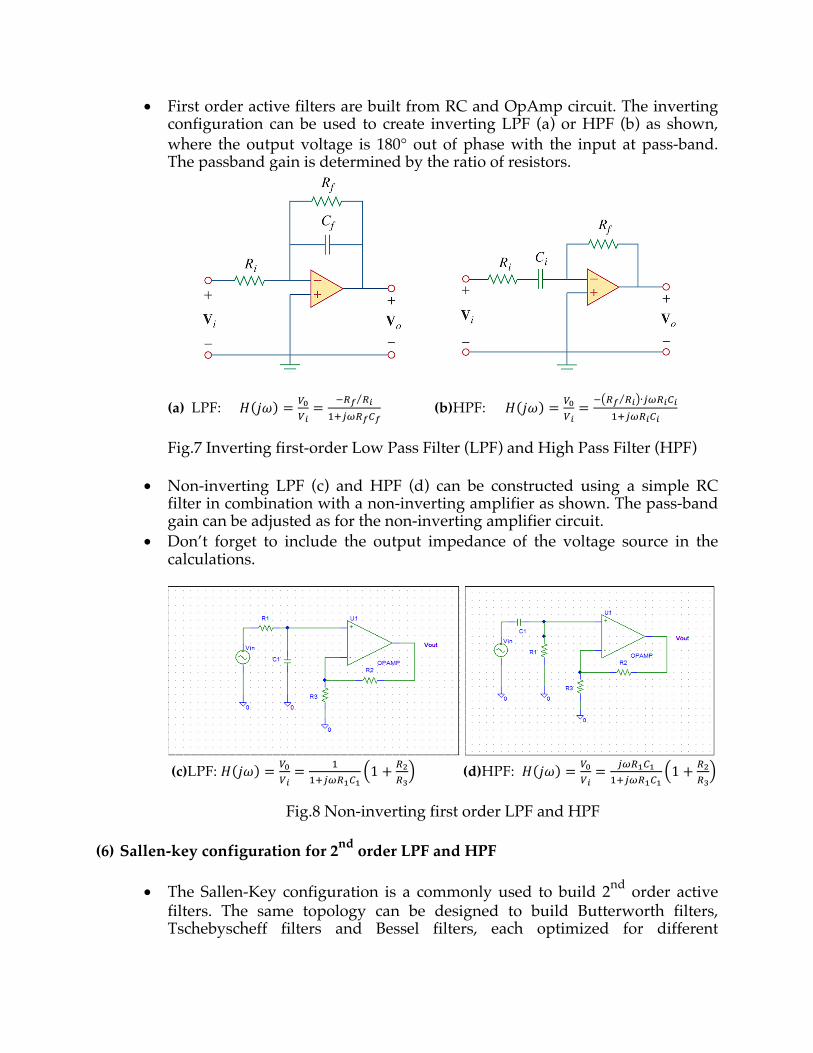
• First order active filters are built from RC and OpAmp circuit. The inverting configuration can be used to create inverting LPF (a) or HPF (b) as shown, where the output voltage is 180° out of phase with the input at pass-band. The passband gain is determined by the ratio of resistors.
(a) LPF: 𝐻 𝑗𝜔 = !!
!!= !!! !!
!!!"!!!! (b)HPF: 𝐻 𝑗𝜔 = !!
!!= ! !! !! ∙!"!!!!
!!!"!!!!
Fig.7 Inverting first-order Low Pass Filter (LPF) and High Pass Filter (HPF)
• Non-inverting LPF (c) and HPF (d) can be constructed using a simple RC
filter in combination with a non-inverting amplifier as shown. The pass-band gain can be adjusted as for the non-inverting amplifier circuit.
• Don’t forget to include the output impedance of the voltage source in the calculations.
(c)LPF: 𝐻 𝑗𝜔 = !!
!!= !
!!!"!!!!1 + !!
!! (d)HPF: 𝐻 𝑗𝜔 = !!
!!= !"!!!!
!!!"!!!!1 + !!
!!
Fig.8 Non-inverting first order LPF and HPF
(6) Sallen-key configuration for 2nd order LPF and HPF
• The Sallen-Key configuration is a commonly used to build 2nd order active
filters. The same topology can be designed to build Butterworth filters, Tschebyscheff filters and Bessel filters, each optimized for different

characteristics such as passband flatness, cut-off sharpness, and phase linearity.
• The LPF and HPF Sallen-Key topology simply switch the relative R and C positions.
• Sallen-Key filters can be cascaded to build higher-order filters. Consult a filter-design website such as http://www.analog.com/designtools/en/filterwizard/#/type to determine component values.
LPF: 𝐻 𝑗𝜔 = !!
!!= !
!!!(!!!!!!!!!!" !!!!! !!!!
Fig.9 2nd order Sallen Key configuration LPF
Reference:
1. OP741data sheet: www.ti.com/product/lm741 2. MCP6001data sheet: ww1.microchip.com/downloads/en/devicedoc/21733f.pdf 3. LM124 data sheet: www.ti.com/product/lm124 4. OP551 data sheet: www.ti.com/lit/gpn/opa552 5. Active Filter design manual: www.ti.com/lit/ml/sloa088/sloa088.pdf 6. Sallen-Key topology: www.ti.com/lit/an/sloa024b/sloa024b.pdf