Embed Size (px)
Citation preview

Determination of the Thermal Noise Limit of Graphene Biotransistors
Crosser, M. S., Brown, M. A., McEuen, P. L., & Minot, E. D. (2015). Determination of the thermal noise limit of graphene biotransistors. Nano Letters, 15(8), 5404-5407. doi:10.1021/acs.nanolett.5b01788
10.1021/acs.nanolett.5b01788
American Chemical Society
Accepted Manuscript
http://cdss.library.oregonstate.edu/sa-termsofuse

1
Determination of the thermal noise limit of graphene
biotransistors
Michael S. Crosser1, Morgan A. Brown
2, Paul L. McEuen
3, Ethan D. Minot
2
1Department of Physics, Linfield College, McMinnville, OR 97128, USA
2Department of Physics, Oregon State University, Corvallis, OR 97331, USA
3Kavli Institute at Cornell for Nanoscale Science, Cornell University, Ithaca, NY 14853, USA
ABSTRACT: To determine the thermal noise limit of graphene biotransistors, we have measured
the complex impedance between the basal plane of single-layer graphene and an aqueous
electrolyte. The impedance is dominated by an imaginary component, but has a finite real
component. Invoking the fluctuation-dissipation theorem, we determine the power spectral
density of thermally-driven voltage fluctuations at the graphene/electrolyte interface. The
fluctuations have 1/𝑓𝑝 dependence, with p = 0.75 - 0.85, and the magnitude of fluctuations scales
inversely with area. Our results explain noise spectra previously measured in liquid-gated
suspended graphene devices, and provide realistic targets for future device performance.
2
Graphene field-effect transistors (GFETs) are a promising platform for many biosensing
applications in liquid environments.1 For example, extracellular voltages associated with action
potentials cause a measurable change in the resistance of a GFET (Karni et al., Hess et al.),
making GFETs attractive for neural recording techniques. The binding of charged molecules,
such as proteins or DNA, can also be measured by GFET biosensors, making GFETs attractive
for next-generation biomarker assays.1
The resolution of GFET sensors is limited by 1/f noise.3 This noise can be traced to
fluctuations in the carrier concentration, n, the carrier mobility, or both. For liquid-gated GFETs
on SiO2, the dominant noise mechanism is the fluctuating occupancy of charge traps in the
dielectric substrate causing fluctuations in n.4 This charge-trap noise can be reduced by removing
the dielectric substrate and leaving the graphene suspended.5 Additionally, “clean” dielectric
materials such as hexagonal boron nitride6 are likely to reduce charge-trap noise. As
improvements in device design reduce charge-trap noise, it is important to determine the intrinsic
limits set by thermal fluctuations. Knowledge of these fundamental limits is needed to set targets
for device performance, and to develop a realistic vision of future applications.
In this work we utilize the fluctuation-dissipation theorem to determine the thermally-driven
“liquid-gate Johnson noise” of GFET biosensors. Similar methodology has previously been
employed to understand the Johnson noise measured from metal microelectrodes in contact with
electrolytes.7,8
Here we apply these ideas to liquid-gated transistors for the first time. First, we
determine the frequency-dependent impedance between an aqueous electrolyte and a graphene
sheet, Z(f), for a number of different graphene devices. These measurements demonstrate that the
graphene-electrolyte interface acts as a dissipative circuit element. This surprising result has
important implications for biosensors as well as other systems, like graphene-based

3
supercapacitors,9 that utilize the graphene-electrolyte interface. After determining Z(f), we use
the fluctuation-dissipation theorem to predict the power spectral density of thermally-driven
voltage fluctuations across such a circuit element,
SV,th(f) = 4kBTZre(f), (1)
where kB is Boltzmann’s constant, T is temperature, and Zre(f) is the real component of the
graphene-liquid impedance. SV,th(f) is independent from the more commonly discussed “channel-
resistance Johnson noise” in GFET devices. SV,th(f) varies with frequency and represents the
lower limit for gate-voltage noise in liquid-gated GFETs.
Graphene on copper foil (ACS Materials) was transferred onto silicon wafers with a 300 nm
oxide layer using a standard wet transfer procedure.10
The graphene was patterned into squares
of various dimensions via photolithography and O2 plasma etching. To minimize the residue
from photoresist,11
a sacrificial layer of a polydimethyl glutarimide resist (LOR-3B from
MicroChem Corporation) was deposited below the photoresist during each lithographic step.
Source and drain contacts (2 nm Cr, 30 nm Au) were patterned via photolithography and electron
beam evaporation (see Fig. 1b).

4
Figure 1. (a) Schematic of the impedance measurement: A dc voltage, Vg, and a small ac
voltage, Vac, are added together to define the liquid gate voltage Vgl. The ac component of the
current, Igl, is measured by the lock-in amplifier. (b) Optical microscope image of a device with
an exposed graphene area of 5040 m2. Photoresist covers the remaining, visible surface. Dotted
lines highlight the edges of the graphene.
To enable measurements of the electrolyte/graphene interface impedance, the metal electrodes
were covered with an insulating layer of photoresist. Windows in the photoresist were patterned
above the graphene (Fig. 1). Devices were fabricated with various electrolyte/graphene contact
areas (ranging from 3000 m2 up to 23,000 m
2). We also tested smaller devices, however,
these tended to trap air bubbles inside the photoresist windows, rendering them unusable. One
graphene device was left fully covered with photoresist so that parasitic capacitance between the
liquid and the metal electrodes could be quantified (see supplementary materials).
We first characterized the devices by measuring dc conductance between the source and drain
electrodes (current flowing from metal to graphene to metal). A droplet of electrolyte was placed
on the chip (10 mM phosphate buffer with pH 7.1). A small bias (25 mV) was applied to the
source electrode and current was collected from the drain electrode. A dc gate voltage, Vg, was
applied to the electrolyte solution using a tungsten wire with surface area much greater than that
of the graphene device. Figure 2a shows a typical conductance curve G(Vg). The conductance
minimum has been shifted so as to occur at gate voltage VD ≈ 0, which we refer to as the Dirac
point. The conductance characteristics are consistent with well-contacted high-quality graphene.
5
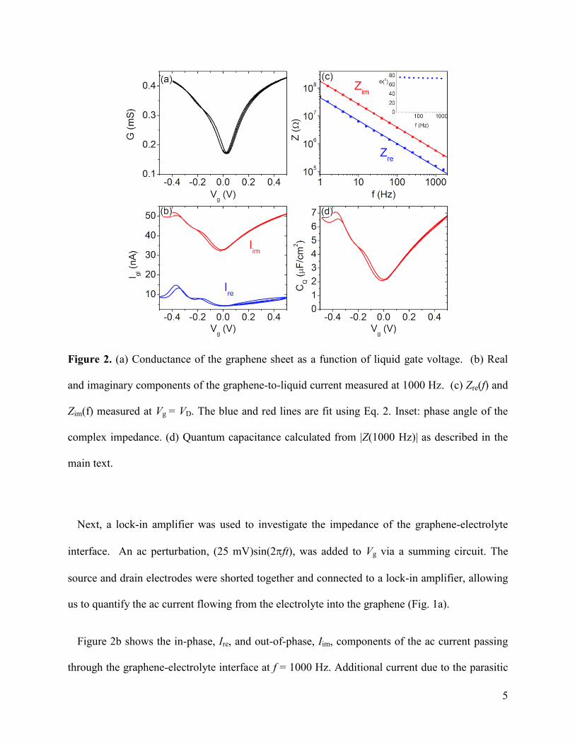
Figure 2. (a) Conductance of the graphene sheet as a function of liquid gate voltage. (b) Real
and imaginary components of the graphene-to-liquid current measured at 1000 Hz. (c) Zre(f) and
Zim(f) measured at Vg = VD. The blue and red lines are fit using Eq. 2. Inset: phase angle of the
complex impedance. (d) Quantum capacitance calculated from |Z(1000 Hz)| as described in the
main text.
Next, a lock-in amplifier was used to investigate the impedance of the graphene-electrolyte
interface. An ac perturbation, (25 mV)sin(2ft), was added to Vg via a summing circuit. The
source and drain electrodes were shorted together and connected to a lock-in amplifier, allowing
us to quantify the ac current flowing from the electrolyte into the graphene (Fig. 1a).
Figure 2b shows the in-phase, Ire, and out-of-phase, Iim, components of the ac current passing
through the graphene-electrolyte interface at f = 1000 Hz. Additional current due to the parasitic
6
capacitance between the liquid and the metal leads has been subtracted (Iimparasitic
= 23 nA at 1000
Hz). For the graphene-electrolyte interface, Iim is approximately 5 times larger than Ire.
The complex impedance of a double-layer capacitor (also known as an electrochemical
capacitor) is commonly observed to be proportional to 1/(𝑖𝑓)𝑝, where 0 < p < 1 and i is the
imaginary unit.12
Expressing this complex impedance in terms of real and imaginary components
gives
𝑍(𝑓) ∝1
𝑓𝑝 (cos (𝑝𝜋
2) − 𝑖 sin (𝑝
𝜋
2)) . (2)
Interestingly, Eq. 2 predicts that a single parameter, p, can be used to fit both the constant phase
angle, = tan-1
(Zim/Zre) and the exponent of the frequency dependence.
To compare our devices with Eq. 2, we measured Ire and Iim over a range of frequencies and
calculated Zre, Zim, and (Fig. 2c). We limit our analysis to the frequency range 1 – 1000 Hz,
where the impedance of the double-layer capacitor dominates the response of the circuit. (A
series resistance of less than 50 k limits the flow of charge onto the double-layer capacitor at
very high frequency. A parallel resistance of more than 1 G, associated with electrochemical
charge transfer, shunts the double-layer capacitor at very low frequency.) Coincidentally, 1 –
1000 Hz is the frequency range of interest for many biosensor applications. Figure 2c shows that
a single fit parameter, p = 0.83, accurately describes both the constant and the power law
relationship between Z and f. Eight additional devices have been characterized and we
consistently find good agreement with Eq. 2, with p ranging from 0.75 to 0.85. This is the first
report of constant for double-layer capacitors made from isolated single-layer graphene.
At f = 1000 Hz, the observed magnitude of the graphene-electrolyte impedance, |Z|, is
consistent with previous work by Xia et al.13
Xia et al. model the interface as two capacitances
7
acting in series: (1) the quantum capacitance of the graphene, CQ, which is proportional to the
density of state at the Fermi level and therefore tunable by Vg, and (2) the capacitance of the
ionic double layer, Cdl. For our experimental conditions, Cdl ≈ 16 F/cm2.14
The total capacitance
is then
Ctot = (Cdl-1
+ CQ-1
)-1
. (3)
We equate Ctot with the measured quantity 1/2𝜋𝑓|𝑍(𝑓)| and use Eq. 3 to estimate CQ for our
graphene devices (Fig. 2d). The minimum value of CQ is 2 F/cm2, and the maximum slope is
|dCQ/dVg| = 18 F/V∙cm2. These values agree well with existing models for the density of states
of single-layer graphene (see Supporting Information for further discussion). We conclude that
our measurements at 1000 Hz exhibit the signatures of single-layer graphene, but note that
existing theory fails to explain < 90° and |Z| ∝1/𝑓𝑝.
Once Zre(f) is determined (Fig. 2c), it is straightforward to apply Eq. 1 to predict the power
spectral density of the voltage noise across the graphene/electrolyte interface (Fig. 3). Note that
the frequency dependence of Zre predicts a 1/𝑓𝑝 spectrum for the thermally-driven liquid-gate
noise. This noise spectrum is strikingly different from the white noise that Eq. 1 predicts for an
ideal resistor. It is interesting that the Johnson noise predicted by Eq. 1 can range from white
noise to close to 1/f noise depending on the specific Zre(f) of the system.

8
Figure 3. Predicted power spectral density of the liquid-gate Johnson noise (Eq. 1) for the
device featured in Fig. 2c.
We have measured Zre(f) for 8 devices, with a variety of sizes and gating conditions. These
measurements are summarized in Fig. 4, where we plot SV,th(1 Hz) for each device. For
comparison, we also plot previously-measured SV(1 Hz) values obtained from time-domain
measurements of the conductance fluctuations in GFETs (further discussion below). The right-
hand axis of Fig. 4 shows the equivalent voltage resolution, Vres, for a given value of SV. We
define Vres as √∫ 𝑆𝑉(𝑓)𝑑𝑓 and use the approximation Vres ≃ √𝑆𝑉(1 Hz) ⋅ 1 Hz. This approximation
is valid for a measurement bandwidth that spans one decade of frequency.

9
Figure 4. Plot of gate voltage noise power spectral density versus area for eight devices (this
work), and a comparison with previous work on liquid-gated GFETs. The dark blue circles were
measured with Vg = VD. The light blue circles were measured at Vg = VD + 0.8 V. The solid line
with slope A-1
shows our estimate for the thermal noise limit. For comparison, we plot the power
spectral densities reported by other authors who measured similar GFET biosensors. Solid
symbols correspond to GFET devices on oxide surfaces. Open symbols correspond to suspended
GFET devices.
We first discuss the relationship between SV,th and the graphene surface area, A. As expected,
we observe that Zre (and therefore SV,th) scales inversely with A. Previous measurements of noise
in GFETs,4,5,15
and related systems such as metal electrodes,7 show the same trend. The
relationship SV µ A-1
summarizes the trade-off between voltage resolution and spatial resolution.
10
Our results show that SV,th can be modified by gate voltage. Increasing Vg adds carriers to the
graphene and decreases both Zim and Zre with minimal change in (see Supporting Information).
For highly-doped graphene, Zre (and therefore SV,th) is several times smaller than in lightly-doped
graphene. Using the highly-doped values of SV,th, we have estimated the “thermal noise limit” for
graphene when p = 0.85 (solid line in Fig. 3 with slope A-1
).
Our results are consistent with previous reports of gate voltage fluctuations in GFET
biosensors. Previous measurements were sensitive to the sum of SV,th and extrinsic noise SV,ext.
We define the total noise power spectral density as
SV = SV,th + SV,ext, (4)
where SV,ext is due to mechanisms such as the fluctuating occupancy of charge traps in the
dielectric substrate. For GFETs on an SiO2 substrate, SV,ext dominates the noise spectrum;5
therefore, we expect SV > SV,th for such devices (see Fig. 3). In suspended GFETs (where the
SiO2 substrate has been removed) SV is reduced. Cheng et al.5 report one device with SV equal to
our estimated thermal noise limit (see Fig. 3). The frequency dependence of the noise spectrum
in Cheng’s device, 1/𝑓0.9, is consistent with Eq. 2 (p < 1). Other suspended GFET devices have
been measured with SV > SV,th (red open symbols in Fig. 3).15
These devices were likely “dirty”
due to contact with mouse hearts (proteins and other biomolecules on the graphene surface
contribute to SV,ext16
). We conclude that our work provides a framework for understanding the
noise limit reached by clean suspended graphene FETs.
Finally, we comment on the performance of GFET biosensors compared to other materials.
The thermally-limited voltage resolution of GFET sensors is surprisingly similar to metal
electrodes.7,8
The measurements we report here elucidate the origin of this similarity. Both the
graphene-electrolyte interface and the metal-electrolyte interface are imperfect capacitors. In

11
both cases, the thermal noise is determined by Zre, which is linked (via Eq 2, and the parameter
p) to the double-layer capacitance of an aqueous electrolyte in contact with a smooth conducting
surface.
We conclude that standard GFET devices operating in liquid environments face voltage noise
limits that are similar to those of metal electrodes. To reach lower noise levels, researchers will
have to explore new ways of increasing p, the parameter describing the ideality of the double-
layer capacitance. The microscopic mechanism responsible for p < 1 is currently not understood,
therefore, future research into this mechanism has the potential to impact both biosensor
applications as well as other applications that utilize graphene-electrolyte interfaces. Regardless
of future efforts to increase p, GFET biosensors hold great promise. Graphene offers remarkable
mechanical flexibility and biocompatibility, and, in contrast to metal microelectrodes, FETs offer
local amplification of weak signals. Local amplification is useful in applications such as high
channel count neural recording where weak signals must be boosted before transmission to data
acquisition hardware. With this strong set of properties, GFET devices are extremely promising
for next-generation biosensors.
Supporting Information. Control experiments to determine parasitic capacitance. Quantum
capacitance of single-layer graphene. Z(f) for devices of different area. Phase angle as a function
of gate voltage. Source-drain current fluctuations caused by liquid-gate Johnson noise compared
to fluctuations caused by channel-resistance Johnson noise. This material is available free of
charge via the Internet at http://pubs.acs.org.
Corresponding Author. Ethan D. Minot. E-mail: [email protected]
12
Acknowledgements. Funding for this research was provided by the National Science
Foundation under award number DBI-1450967.
References
(1) Liu, Y.; Dong, X.; Chen, P. Chem. Soc. Rev. 2012, 41 (6), 2283–2307.
(2) Hubel, D. Science 1957, 125 (3247), 549–550.
(3) Balandin, A. Nat. Nanotechnol. 2013, 8 (8), 549–555.
(4) Heller, I.; Chatoor, S.; Männik, J.; Zevenbergen, M. a G.; Oostinga, J. B.; Morpurgo, A.
F.; Dekker, C.; Lemay, S. G. Nano Lett. 2010, 10 (5), 1563–1567.
(5) Cheng, Z.; Li, Q.; Li, Z.; Zhou, Q.; Fang, Y. Nano Lett. 2010, 10 (5), 1864–1868.
(6) Petrone, N.; Dean, C. R.; Meric, I.; van der Zande, A. M.; Huang, P. Y.; Wang, L.;
Muller, D.; Shepard, K. L.; Hone, J. Nano Lett. 2012, 12 (6), 2751–2756.
(7) Gesteland, R.; Howland, B.; Lettvin, J. Y.; Pitts, W. H. Proc. IRE 1959, 47 (11).
(8) Robinson, D. A. Proc. IEEE 1968, 56 (6), 1065–1071.
(9) Stoller, M. D.; Park, S.; Zhu, Y.; An, J.; Ruoff, R. S. Nano Lett. 2008, 6–10.
(10) Saltzgaber, G.; Wojcik, P.; Sharf, T.; Leyden, M. R.; Wardini, J. L.; Heist, C. a; Adenuga,
A. a; Remcho, V. T.; Minot, E. D. Nanotechnology 2013, 24 (35), 355502.
(11) Lerner, M. B.; Matsunaga, F.; Han, G. H.; Hong, S. J.; Xi, J.; Crook, A.; Perez-Aguilar, J.
M.; Park, Y. W.; Saven, J. G.; Liu, R.; Johnson, a T. C. Nano Lett. 2014, 14 (5), 2709–
2714.
(12) Kötz, R.; Carlen, M. Electrochim. Acta 2000, 45, 2483–2498.
(13) Xia, J.; Chen, F.; Li, J.; Tao, N. Nat. Nanotechnol. 2009, 4 (8), 505–509.
(14) Rieger, P. Electrochemistry, 2nd ed.; Chapman & Hall: New York, 1994.
(15) Cheng, Z.; Hou, J.; Zhou, Q.; Li, T.; Li, H.; Yang, L.; Jiang, K.; Wang, C.; Li, Y.; Fang,
Y. Nano Lett. 2013, 13 (6), 2902–2907.

13
(16) Sharf, T.; Kevek, J. W.; Deborde, T.; Wardini, J. L.; Minot, E. D. Nano Lett. 2012, 12
(12), 6380–6384.