Embed Size (px)
Citation preview

DETECTION OF RESIDUAL STRESS IN SiC MEMS USING µ-RAMAN SPECTROSCOPY
THESIS
John C. Zingarelli, First Lieutenant, USAF
AFIT/GEO/ENP/05-06
DEPARTMENT OF THE AIR FORCE AIR UNIVERSITY
AIR FORCE INSTITUTE OF TECHNOLOGY
Wright-Patterson Air Force Base, Ohio
APPROVED FOR PUBLIC RELEASE; DISTRIBUTION UNLIMITED

The views expressed in this thesis are those of the author and do not reflect the official policy or position of the United States Air Force, Department of Defense, or the United States Government.
AFIT/GEO/ENP/05-06
DETECTION OF RESIDUAL STRESS IN SiC MEMS USING µ-RAMAN SPECTROSCOPY
THESIS
Presented to the Faculty
Department of Engineering Physics
Graduate School of Engineering Physics
Air Force Institute of Technology
Air University
Air Education and Training Command
in Partial Fulfillment of the Requirements for the
Degree of Master of Science in Electrical Engineering
John C. Zingarelli, B.S.E.E.
First Lieutenant, USAF
March 2002
APPROVED FOR PUBLIC RELEASE; DISTRIBUTION UNLIMITED


AFIT/GEO/ENP/05-06
Abstract
Micro-Raman (µ-Raman) spectroscopy is used to measure residual stress in two sil-
icon carbide (SiC) poly-types: single-crystal, hexagonally symmetric 6H-SiC, and poly-
crystalline, cubic 3C-SiC thin films deposited on Si substrates. Both are used in micro-
electro-mechanical-systems (MEMS). The 6H-SiC structures are bulk micro-machined
by back etching a 250-µm-thick, single-crystal 6H-SiC wafer (p-type, 7 Ω-cm, 3.5 off-
axis) to form a 50-µm thick diaphragm. A Wheatstone bridge, patterned of piezoresistive
elements, is formed across the membrane from a 5-µm, 6H-SiC (n-type, doped 3.8 x
1018cm−3) epilayer; the output of the bridge is proportional to the flexure of the MEMS
diaphragm. For these samples, the µ-Raman spectroscopy is performed using a Renishaw
InVia Raman spectrometer with an argon-ion excitation source (λ = 514.5 nm, hν = 2.41
eV) with an approximate 1-µm2 spot size through the 50x objective. By employing an
incorporated piezoelectric stage with submicron positioning capabilities along with the
Raman spectral acquisition, spatial scans are performed to reveal areas in the MEMS
structures that contain residual stress. Shifts in the transverse optical (TO) Stokes peaks
of up to 1 cm−1 along the edge of the diaphragm and through the piezoresistors indicate
significant material strain induced by the MEMS fabrication process. The phonon defor-
mation potential in both SiC poly-types is measured to quantify the material stress as a
function of the shift in the Raman peak position. The line center of the TO Stokes peak
is shifted by applying a uniform stress to the sample using a four-point strain fixture and
monitoring the applied stress using a strain gauge, while the µ-Raman spectrum is be-
ing measured. A spectral analysis code tracks the shift of the Raman peak position with
respect to the line center of the Rayleigh peak to account for any thermal drift of the spec-
trometer during the time of the area scan. 3C-SiC films, with thicknesses ranging from
1.5-5 µm and are deposited by chemical vapor deposition on (100) Si substrates, are also
investigated to determine their residual stress via their Raman spectral characteristics. An
iv
ultraviolet excitation source (λ = 325 nm, hν = 3.82 eV) is determined to be more effective
for the detection of Raman shifts in these thin films than the 514-nm source, do to both
resonant Raman effects and since the absorption coefficient in SiC at 300 K at 325 nm
is 3660 cm−1, while that at 514 nm is less than 100 cm−1 (dependent on doping level).
In addition, the Si substrate is less Raman active at 325-nm excitation, leading to a lower
relative amplitude than that at 514.5 nm and increasing the signal-to-noise ratio (SNR) of
the SiC Raman spectrum. Since SNR is also increased by increasing absorption length,
the thicker films (5.5 µm) of the 3C-SiC are preferable for measuring Raman spectra than
the thinner films (1.5 µm).
v

Acknowledgements
The most notable part of my research has been the interaction with so many brilliant and
motivated scientists. For the guidance and support making this research possible, I would
like to especially thank my advisor Dr. Michael A. Marciniak and Capt LaVern Starman.
For the funding and hours of time discussing and analyzing results my appreciation goes
to Mr. Jason Foley. For providing samples, materials, data and ideas, I thank Jeff Melzak.
Other people I would like to mention who helped me in numerous ways were Capt Tetsuo
Kaieda, Jason Reber, John Busbee, David Liptak, Mr.William Fitzgerald Phil Neudack,
and Tim Prusnick. Finally and most importantly I would like to thank my wife for her
loving support.
John C. Zingarelli
vi
Table of ContentsPage
Abstract . . . . . . . . . . . . . . . . . . . . . . . . . . . . . . . . . . . . . . iv
Acknowledgements . . . . . . . . . . . . . . . . . . . . . . . . . . . . . . . . vi
List of Figures . . . . . . . . . . . . . . . . . . . . . . . . . . . . . . . . . . . x
List of Tables . . . . . . . . . . . . . . . . . . . . . . . . . . . . . . . . . . . xv
List of Abbreviations . . . . . . . . . . . . . . . . . . . . . . . . . . . . . . . xvi
I. Introduction . . . . . . . . . . . . . . . . . . . . . . . . . . . . . . . 1-1
1.1 Motivation . . . . . . . . . . . . . . . . . . . . . . . . . . 1-1
1.1.1 Applications: SiC Electronic devices . . . . . . . 1-2
1.1.2 Applications: SiC MEMS . . . . . . . . . . . . . 1-2
1.2 Current technology limitations . . . . . . . . . . . . . . . . 1-4
1.3 Problem Statement and Research Objectives . . . . . . . . 1-5
1.4 Thesis Organization . . . . . . . . . . . . . . . . . . . . . 1-5
II. Background Information . . . . . . . . . . . . . . . . . . . . . . . . 2-1
2.1 µ−Raman Spectroscopy . . . . . . . . . . . . . . . . . . . 2-1
2.2 Residual Stress . . . . . . . . . . . . . . . . . . . . . . . . 2-4
2.3 Detection of Residual Stress in poly-Si . . . . . . . . . . . 2-5
2.4 Background Information on SiC . . . . . . . . . . . . . . . 2-9
2.5 Fabrication of SiC MEMS . . . . . . . . . . . . . . . . . . 2-11
2.6 Crystal Defects of SiC . . . . . . . . . . . . . . . . . . . . 2-14
2.6.1 Point Defects . . . . . . . . . . . . . . . . . . . . 2-14
2.6.2 Line Defects . . . . . . . . . . . . . . . . . . . . 2-15
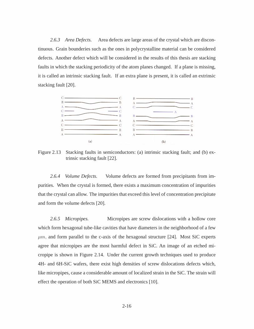
2.6.3 Area Defects . . . . . . . . . . . . . . . . . . . . 2-16
2.6.4 Volume Defects . . . . . . . . . . . . . . . . . . 2-16
2.6.5 Micropipes . . . . . . . . . . . . . . . . . . . . . 2-16
2.7 Literature Review . . . . . . . . . . . . . . . . . . . . . . 2-17
2.8 Chapter Summary . . . . . . . . . . . . . . . . . . . . . . 2-21
vii

Page
III. Samples . . . . . . . . . . . . . . . . . . . . . . . . . . . . . . . . . 3-1
3.1 NASA crystalline 6H-SiC accelerometer and pressure sensor 3-1
3.1.1 Layout and Function . . . . . . . . . . . . . . . . 3-1
3.1.2 Resistivity of the piezoresistors #2 and #4 . . . . 3-2
3.2 Cree 6H-SiC wafers . . . . . . . . . . . . . . . . . . . . . 3-6
3.3 FLX poly-SiC Thin Films . . . . . . . . . . . . . . . . . . 3-6
3.3.1 1.5-µm SiC on Si . . . . . . . . . . . . . . . . . 3-7
3.3.2 5.5-µm SiC on Si . . . . . . . . . . . . . . . . . 3-7
3.3.3 Optical Properties of SiC . . . . . . . . . . . . . 3-8
3.4 Chapter Summary . . . . . . . . . . . . . . . . . . . . . . 3-9
IV. Equipment and Experiments . . . . . . . . . . . . . . . . . . . . . . 4-1
4.1 Probe Station . . . . . . . . . . . . . . . . . . . . . . . . . 4-1
4.2 Scanning Electron Microscope . . . . . . . . . . . . . . . . 4-2
4.2.1 AMRAY 1810 (1990) . . . . . . . . . . . . . 4-3
4.3 Zygo Interferometer . . . . . . . . . . . . . . . . . . . . . 4-4
4.4 InVia Raman Spectrometer . . . . . . . . . . . . . . . . . 4-4
4.4.1 Spectral Resolution . . . . . . . . . . . . . . . . 4-5
4.4.2 Sampling Rate . . . . . . . . . . . . . . . . . . . 4-7
4.5 Four-point Strain Fixture . . . . . . . . . . . . . . . . . . . 4-8
4.6 Vice . . . . . . . . . . . . . . . . . . . . . . . . . . . . . . 4-9
4.7 P-3 Strain Indicator and Recorder . . . . . . . . . . . . . . 4-10
4.8 Chapter summary . . . . . . . . . . . . . . . . . . . . . . 4-11
V. Results and Data Analysis . . . . . . . . . . . . . . . . . . . . . . . 5-1
5.1 NASA 550 and 650 6H-SiC MEMS . . . . . . . . . . . . . 5-1
5.1.1 Resistance of piezoresistors . . . . . . . . . . . . 5-1
5.1.2 SEM’s . . . . . . . . . . . . . . . . . . . . . . . 5-2
5.1.3 Zygo Interferometer Data . . . . . . . . . . . . . 5-4
5.1.4 Raman Spectroscopy on the NASA 550 MEMS . 5-6
5.1.5 Phonon Deformation Potential . . . . . . . . . . . 5-8
5.1.6 Raster Maps of Raman Shift . . . . . . . . . . . . 5-15
5.2 Thin Film poly-SiC . . . . . . . . . . . . . . . . . . . . . 5-20
5.2.1 325-nm versus 514-nm Excitation–Resonant Ra-man, Resolution and Luminescence . . . . . . . . 5-20
5.2.2 UV Raman Spectroscopy: Si versus SiC on Si . . 5-21
5.2.3 Film Thickness – Absorption . . . . . . . . . . . 5-22
viii
Page
5.2.4 Substrate Raman Noise . . . . . . . . . . . . . . 5-23
5.2.5 Stacking Faults in poly-SiC . . . . . . . . . . . . 5-25
5.2.6 Delaminated poly-SiC . . . . . . . . . . . . . . . 5-25
5.3 Chapter Summary . . . . . . . . . . . . . . . . . . . . . . 5-27
VI. Conclusions and Recommendations . . . . . . . . . . . . . . . . . . 6-1
6.1 Conclusions . . . . . . . . . . . . . . . . . . . . . . . . . 6-1
6.2 Recommendations for Future Work . . . . . . . . . . . . . 6-2
Appendix A. Properties of SiC . . . . . . . . . . . . . . . . . . . . . . . A-1
Appendix B. Equipment . . . . . . . . . . . . . . . . . . . . . . . . . . B-1
Appendix C. Matlab Code . . . . . . . . . . . . . . . . . . . . . . . . . C-1
C.1 Resistivity Program . . . . . . . . . . . . . . . . . . . . . C-1
C.2 Transmission Program . . . . . . . . . . . . . . . . . . . . C-2
C.3 Raman Analysis Program . . . . . . . . . . . . . . . . . . C-3
Bibliography . . . . . . . . . . . . . . . . . . . . . . . . . . . . . . . . . . . BIB-1
ix
List of FiguresFigure Page
1.1. Pressure Sensor reported to exhibit stable operation at 500oC . . . 1-3
1.2. Cross section of a typical gas turbine engine showing atomizer in-sertion points . . . . . . . . . . . . . . . . . . . . . . . . . . . . . 1-4
2.1. Schematic depicting the Raman and Rayleigh scattering of an exci-taion source due to phonon or vibrational energy present betweentwo atoms. . . . . . . . . . . . . . . . . . . . . . . . . . . . . . . 2-2
2.2. Energy levels for normal Raman, resonance Raman, and fluorescecespectra. . . . . . . . . . . . . . . . . . . . . . . . . . . . . . . . 2-4
2.3. "Frequency shift of the hydrostatic component for an applied uni-axial stress applied along a 1.5 µm-thick Poly2 cantilever with di-mensions of 200 µm-wide by approximately 4000 µm-long." . . . 2-6
2.4. "Background residual stress profiles for a 100 µm-long by 10 µm-wide unreleased and released fixed-fixed beam. (a) Poly1 beam, (b)Poly2 beam and (c) Poly1-Poly2 stacked beam." . . . . . . . . . . 2-7
2.5. "Analytical stress model for a MEMS fixed-fixed beam." . . . . . . 2-8
2.6. "Analytical stress profile of a fixed-fixed beam with a uniform load" 2-9
2.7. Lattice structure of cubic and hexagonal SiC. . . . . . . . . . . . . 2-10
2.8. Representation of stacking order for 6H-SiC. . . . . . . . . . . . . 2-11
2.9. "Cross-section schematic if a SiC micromotor fabricated using theMUSIC process" . . . . . . . . . . . . . . . . . . . . . . . . . . 2-13
2.10. “SEM micrograph of a SiC sallent-pole micromotor fabricated us-ing the MUSIC process." . . . . . . . . . . . . . . . . . . . . . . 2-13
2.11. Point defect. (a) Substitutional impurity. (b) Interstitial impurity.(c) Lattice vacancy. (d) Frenkel-type defect. . . . . . . . . . . . . 2-15
2.12. (a) Edge and (b) screw dislocations in cubic crystals. . . . . . . . . 2-15
2.13. Stacking fault in semiconductor. (a) Intrinsic stacking fault. (b)Extrinsic stacking fault. . . . . . . . . . . . . . . . . . . . . . . . 2-16
2.14. Etched micropipe in a SiC diaphragm. . . . . . . . . . . . . . . . 2-17
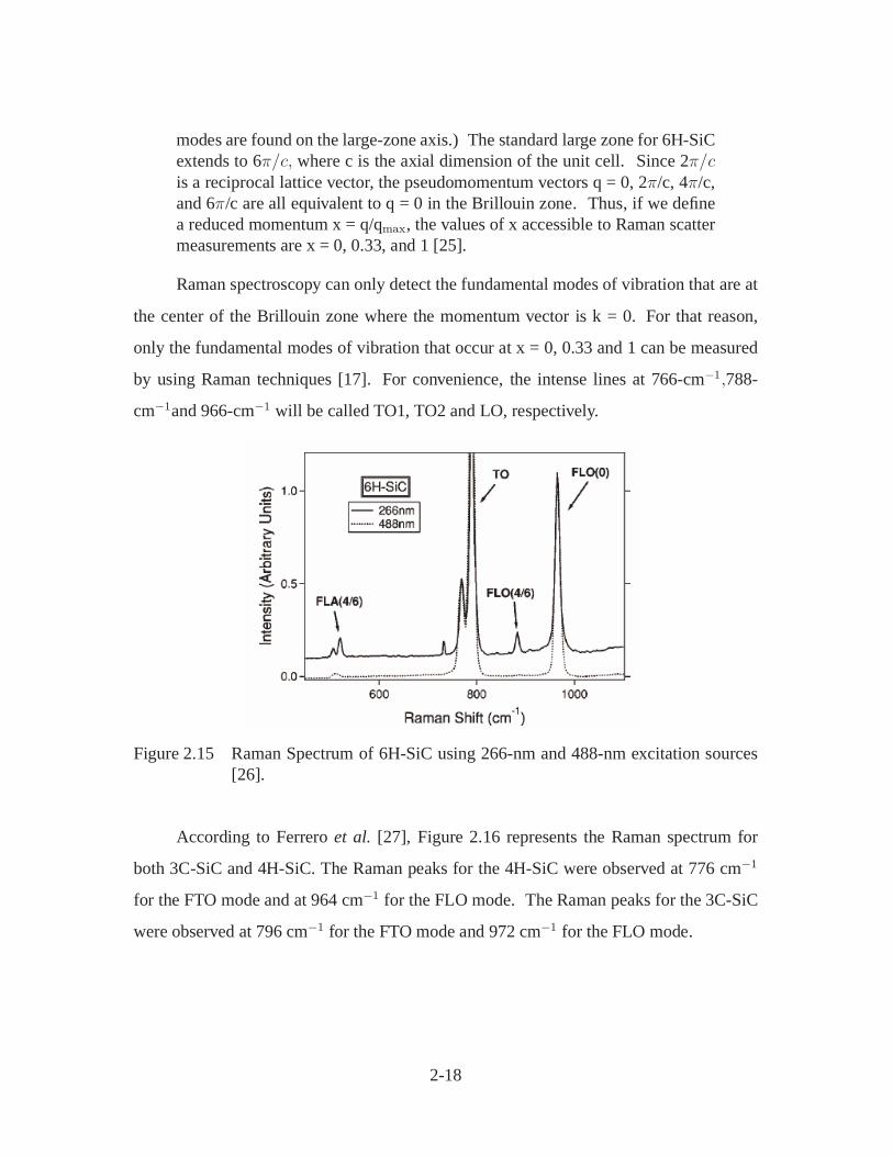
2.15. Raman Spectrum of 6H-SiC using 266-nm and 488-nm exciationsources. . . . . . . . . . . . . . . . . . . . . . . . . . . . . . . . . 2-18
2.16. Raman spectra, 3C-SiC. . . . . . . . . . . . . . . . . . . . . . . . 2-19
2.17. The transversal optical (TO) mode of bulk poly-3C-SiC by Lee etal. [1]. . . . . . . . . . . . . . . . . . . . . . . . . . . . . . . . . 2-20
2.18. µ−stress maps collected of the epitaxially grown 3C-SiC film btLee et al. [1]. . . . . . . . . . . . . . . . . . . . . . . . . . . . . . 2-20
2.19. TO peak in 3C poly-SiC (a) as deposited and (b) after laser anneal-ing at 1700 K. . . . . . . . . . . . . . . . . . . . . . . . . . . . . 2-21
x
Figure Page
3.1. (a) Cross-section of 6H-SiC MEMS diaphragm indicating points ofstress from a shock. (b) Layout of the resistive elements forminga Wheatstone bridge. (c) Top view of the NASA 600 sample withhighlights over the piezoresistive elements. . . . . . . . . . . . . . 3-2
3.2. The resistance of piezoresistors #2 and #4, which are PECVD de-posited 6H-SiC strips of 5-µm epitaxial layers (n-type, doped 3.8×1018cm−3) on the top surface of the wafer. The length of the resis-tors is l = 400 µm and the cross-sectional area is A = 40µm× 5µm.The dopant for the epitaxial layer is N. . . . . . . . . . . . . . . . 3-5
3.3. Layout and specifications of two Cree 6H-SiC wafers used to de-termine phonon deformation potentials. . . . . . . . . . . . . . . . 3-6
3.4. (a) Cross-section of the 1.5µm thick poly-SiC deposited by low-pressure chemical vapor deposition (LPCVD) on a Si substrate. (b)Microscope image of the top of the FLX micro 1.5-µm poly-SiCon a Si substrate. The comb drive is a metal mask deposited ontothe thin film. . . . . . . . . . . . . . . . . . . . . . . . . . . . . . 3-7
3.5. (a) A cross-section of the 5.5µm thick poly-SiC deposited by low-pressure chemical vapor deposition (LPCVD) on a Si substrate.The Si subtrate is back-etched to produce a suspended membraneof SiC. (b) Optical micrograph of the top surface of the 5.5µm thinfilm. The membrane was fractured during transport and droped be-low the support stucture revealing the edge of the diaphragm. Intactsamples were used for all Raman measurements. . . . . . . . . . . 3-8
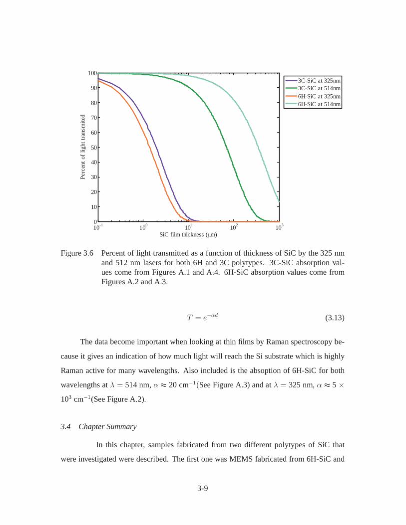
3.6. Percent of light transmitted as a function of thickness of SiC bythe 325 nm and 512 nm lasers for both 6H and 3C polytypes. 3C-SiC absorption values come from Figures A.1 and A.4. 6H-SiCabsorption values come from Figures A.2 and A.3. . . . . . . . . . 3-9
4.1. Four-point probe station used to measure the resistance of piezore-sistive elements. . . . . . . . . . . . . . . . . . . . . . . . . . . . 4-1
4.2. The text boxes label the measurement taken and the arrows indicatewhere the probe needle for the resistance measurement was placedon the device. . . . . . . . . . . . . . . . . . . . . . . . . . . . . 4-2
4.3. AMRAY 1810 SEM. . . . . . . . . . . . . . . . . . . . . . . . . . 4-3
4.4. Diagram of the New View Zygo interferometer system. . . . . . . 4-4
4.5. Diagram of a Renishaw Raman spectrometer. . . . . . . . . . . . . 4-5
4.6. (a) Raman spectrum of diamond powder using a 325-nm excitationsource. (b) Raman peak of diamond powder at 1331 cm−1 showingthe range between sampling points. (c) Raman spectrum of 6H-SiCusing a 514-nm excitation source. (d) LO peak of 6H-SiC a 966cm−1 using a 325-nm excitation source. . . . . . . . . . . . . . . . 4-8
4.7. (a) Top view of the four-point strain fixture. (b) Sideview of thefour-point strain fixture. . . . . . . . . . . . . . . . . . . . . . . . 4-9
4.8. Vice setup used to apply stress to a 1-cm x 1-cm square of 6H-SiCwith a strain gauge epoxyed to the back side and used to measurethe phonon deformation potentials. . . . . . . . . . . . . . . . . . 4-10
xi
Figure Page
4.9. Photograph of the P-3 strain indicator and recorder. . . . . . . . . 4-11
5.1. (a) SEM of the NASA 550 pressure sensor in packaging at 11.3Xmagnification. (b) SEM at 33.2X magnification (c) SEM of resis-tors #2 and #4 at 123X magnification (d) Closeup of resistor #2where a residual stress was identified using Raman spectroscopy. . 5-3
5.2. (a) SEM of resistor #3 on the NASA 550 pressure sensor in thelocation where it crosses the diaphragm. (b) SEM of the NASA550 pressure sensor showing the location of (a) . . . . . . . . . . . 5-4
5.3. An interferogram and a optical micrograph of the resistors #2 and#4 on the NASA 550 sample in a location where isolated residualstress was detected using Raman analysis. . . . . . . . . . . . . . 5-5
5.4. An interferogram and an optical micrograph of resistor # 3 on theNASA 550 sample. Residual stress was identifed where the resistorcrosses the diaphragm by using Raman spectroscopy. . . . . . . . 5-5
5.5. (a) Raman spectrum of crystalline 6H-SiC with a 514-nm excitationsource using the InVia Renishaw spectrometer. (b) Raman spec-trum of crystalline 6H-SiC with a 325-nm excitation source. . . . . 5-7
5.6. 6H-SiC Raman spectrum from the edge of the NASA 550 pressuresensor. . . . . . . . . . . . . . . . . . . . . . . . . . . . . . . . . 5-8
5.7. The top graph shows the line center of the TO2 peak as a functionof uniaxial pressure applied normal to the c-axis of 6H-SiC. Thebottom graph shows the residuals of the linear least squares fit tothe measured data points. . . . . . . . . . . . . . . . . . . . . . . 5-10
5.8. The top graph shows the line center of the TO1 peak as a functionof uniaxial pressure applied normal to the c-axis of 6H-SiC. Thebottom graph shows the residuals of the linear least squares fit tothe measured data points. . . . . . . . . . . . . . . . . . . . . . . 5-11
5.9. (a) Location of line scan on resistor #3. (b) Location of resistor #3on NASA 550 pressure sensor. . . . . . . . . . . . . . . . . . . . 5-12
5.10. The line center of the TO 1 and TO 2 6H-SiC Raman peaks as afunction of position. . . . . . . . . . . . . . . . . . . . . . . . . . 5-13
5.11. The estimated amount of residual stress as a function of position ofthe line scan shown in Figure 5.9. The estimates where found usingphonon deformation potentials for the TO 1 and TO 2 peaks andmapping them to the results shown in Figure 5.10. . . . . . . . . . 5-14
5.12. Typical Raman spectrum of the 6H-SiC as measured during the de-termination of the phonon deformation potential. The raised base-line is due to background noise from a piece of foam the samplewas placed on. . . . . . . . . . . . . . . . . . . . . . . . . . . . . 5-15
5.13. (a) Micrograph of diaphragm edge through a 20X objective with acoordinate system that matches the raster map location in (c). (b)Micrograph of the NASA 550 pressure sensor depicting the locationof the edge of the diaphragm. (c) The residual stress measuredusing of a raster scan across the edge of the diaphragm. . . . . . . 5-16
xii
Figure Page
5.14. (a) Micrograph of resistors #2 and #4 through a 20X objective witha coordinate system that matches the raster map location in (c). (b)Micrograph of the NASA 550 pressure sensor depicting the loca-tion of resistors #2 and #4 on the device. (c) The residual stressmeasured using of a raster scan across resistor #2. . . . . . . . . . 5-17
5.15. (a) Micrograph of resistors #2 and #4 through a 20X objective witha coordinate system that matches the raster map location in (c). (b)Micrograph of the NASA 550 pressure sensor depicting the locationof resistors #2 and #4 on the device. (c) The results of a rasterscan across resistor #4 showing the amounts of residual stress inthe resistor. . . . . . . . . . . . . . . . . . . . . . . . . . . . . . . 5-18
5.16. (a) and (b) Zoom in on the defect location on resistor #4 identifed byRaman mapping (c) Observation of the identified defect opticallyby changing the depth of focus on the microscope and recordingthe image. . . . . . . . . . . . . . . . . . . . . . . . . . . . . . . 5-19
5.17. The blue spectral lines are from the Raman spectrum of a 1.5-µmpoly-SiC layer on a (100) Si substrate measured using a 514-nmexcitation source. The red spectral lines are of the same 1.5-µmpoly-SiC film with a 325-nm excitation source. . . . . . . . . . . . 5-21
5.18. The Raman spectrum of a 1.5-µm poly-SiC on a Si (100) substrateis compared with the Raman spectrum of Si (100) both of whichwere excited by a 325-nm excitation source. . . . . . . . . . . . . 5-22
5.19. Raman spectum of poly-SiC films of thickness 1.5 µm and 5.5 µmusing a 325-nm excitation source. . . . . . . . . . . . . . . . . . . 5-23
5.20. (a) A cross-section of a 5.5-µm poly-SiC thin film grown on a (100)Si substrate. Pyramidal pits of the Si substrate were anisotropi-cally back-etched creating suspended membranes of the poly-SiC(Region 1). Portions of the poly-SiC delaminated revealing the Sisubstrate (Region 3). (b) The Raman spectrum of the three regionsshown in the cross-section (a) using a 325-nm excitation source. . 5-24
5.21. The spectrum of 5.5-µm SiC on Si and SiC on Plexiglas. . . . . . . 5-26
5.22. The shift of peaks of 5.5-µm poly-SiC as a function of compressivestress . . . . . . . . . . . . . . . . . . . . . . . . . . . . . . . . . 5-27
A.1. Electron Hall mobility vs. donor density. Used to determine resis-tivity of 6H-SiC piezoresistors. . . . . . . . . . . . . . . . . . . . A-1
A.2. Absorption coefficient of 6H-SiC vs photon energy. Use to deter-mine transmision length of 325-nm photons in crystalline 6H-SiCMEMS. . . . . . . . . . . . . . . . . . . . . . . . . . . . . . . . A-2
A.3. Absorption coefficient of 6H-SiC vs photon energy . Used to deter-mine transmision length of 514-nm photons in crystalline 6H-SiCMEMS. . . . . . . . . . . . . . . . . . . . . . . . . . . . . . . . . A-2
A.4. "Absorption of cubic SiC crystals 1 and 1 (solid) at 300K. Crystal1 is relatively pure; crystal 2 is strongly n-type (perhaps 1019/cm3
donors)" . . . . . . . . . . . . . . . . . . . . . . . . . . . . . . . A-3
xiii
Figure Page
A.5. Band Structure of 3C-SiC. Important minima of the conductionband and maxima of the valence band. . . . . . . . . . . . . . . . A-4
B.1. Four Point Strain Fixture . . . . . . . . . . . . . . . . . . . . . . B-1
B.2. Parameters of InVia Raman spectrometer configured for the 514-nm excitation source . . . . . . . . . . . . . . . . . . . . . . . . . B-2
B.3. Parameters of InVia Raman spectrometer configured for the 325-nm excitation source . . . . . . . . . . . . . . . . . . . . . . . . . B-2
xiv
List of TablesTable Page
2.1. Raman Shift peak locations for common polytypes of SiC [2] . . . 2-5
2.2. Material Properties of 3C and 6H SiC at 300K [3] . . . . . . . . . 2-12
4.1. Renishaw InVia Raman spectrometer advertised capabilities. . . . 4-7
5.1. Measured resistances of the piezoressitors on the NASA 550 and
650 MEMS sensors with the coresponding standarded deviation of
the measurements. . . . . . . . . . . . . . . . . . . . . . . . . . . 5-2
A.1. Absorption coefficients and depth penetration for 3C-SiC [4] . . . A-3
xv
List of AbbreviationsAbbreviation Page
(TO) transverse optical . . . . . . . . . . . . . . . . . . . . . . . . . . . . iv
(SiC) Silicon Carbide . . . . . . . . . . . . . . . . . . . . . . . . . . . . . 1-1
(MEMS) micro-electrical-mechanical systems . . . . . . . . . . . . . . . . 1-1
NASA National Air and Space Adminstration . . . . . . . . . . . . . . . . 1-1
(AFRL/MN) Munitions Directorate Air Force Research Labratory . . . . . 1-1
(JFET) junction field-effect transistor . . . . . . . . . . . . . . . . . . . . 1-2
(MESFET) metal-semiconductor field-effect transistor . . . . . . . . . . . 1-2
(MOSFET) metal-oxide-semiconductor field-effect transistor . . . . . . . . 1-2
(CMOS) complementary MOSFET . . . . . . . . . . . . . . . . . . . . . 1-2
(IC’s) intergrated circuits . . . . . . . . . . . . . . . . . . . . . . . . . . . 1-2
(RF) Radio Frequency . . . . . . . . . . . . . . . . . . . . . . . . . . . . 1-3
(Q) Quality factor . . . . . . . . . . . . . . . . . . . . . . . . . . . . . . . 1-3
(ARA) Applied Research Associates . . . . . . . . . . . . . . . . . . . . . 1-4
(NDE) Non-Destructive Evaluation . . . . . . . . . . . . . . . . . . . . . 1-5
(IR) Infrared . . . . . . . . . . . . . . . . . . . . . . . . . . . . . . . . . 2-3
(AFIT) Air Force Institute of Technology . . . . . . . . . . . . . . . . . . 2-5
(MUSIC) Multi-User Silicon Carbide . . . . . . . . . . . . . . . . . . . . 2-12
(MUMPs) Multi-User MEMS Processes . . . . . . . . . . . . . . . . . . . 2-12
(DRIE) Deep Reactive Ion Etching . . . . . . . . . . . . . . . . . . . . . 2-12
(CVD) chemical vapor deposition . . . . . . . . . . . . . . . . . . . . . . 2-12
(FTO) Folded Transverse Optical . . . . . . . . . . . . . . . . . . . . . . 2-17
(FLO) Folded Longitudnal Optical . . . . . . . . . . . . . . . . . . . . . . 2-17
(PECVD) Plasma Enhanced Chemical Vapor Deposition . . . . . . . . . . 3-2
(N) Nitrogen . . . . . . . . . . . . . . . . . . . . . . . . . . . . . . . . . 3-2
(poly-SiC) polycrystalline 3C-SiC . . . . . . . . . . . . . . . . . . . . . . 3-6
xvi
Abbreviation Page
(LPCVD) low-pressure chemical vapor deposition . . . . . . . . . . . . . 3-6
(SiO2) Silicon Dioxide . . . . . . . . . . . . . . . . . . . . . . . . . . . . 3-7
(Si3N4) Silicon Nitride . . . . . . . . . . . . . . . . . . . . . . . . . . . . 3-7
(KOH) Potassium hydroxide . . . . . . . . . . . . . . . . . . . . . . . . . 3-7
(I-V) current-voltage . . . . . . . . . . . . . . . . . . . . . . . . . . . . . 4-1
(SEM) Scaning Electron Microscope . . . . . . . . . . . . . . . . . . . . 4-2
(PC) personal computer . . . . . . . . . . . . . . . . . . . . . . . . . . . 4-3
(UV) ultra violet . . . . . . . . . . . . . . . . . . . . . . . . . . . . . . . 5-6
(FTO) Folded Transverse Optical . . . . . . . . . . . . . . . . . . . . . . 5-7
(FLO) Folded Longitudnal Optical . . . . . . . . . . . . . . . . . . . . . . 5-7
(SNR) signal to noise ratio . . . . . . . . . . . . . . . . . . . . . . . . . . 5-20
xvii
DETECTION OF RESIDUAL STRESS IN SiC MEMS USING
µ−RAMAN SPECTROSCOPY
I. Introduction
Silicon Carbide (SiC) mi cro-electro-mechanical-systems (MEMS) structures are
being studied by NASA Glenn Research Center researchers in conjunction with the Mu-
nitions Directorate, Air Force Research Laboratory (AFRL/MN) as engine pressure sen-
sors/accelerometers for munition fuzes. SiC is recognized for its superior mechanical,
electrical and chemical properties, making it a good choice for applications in the harsh
environments of these applicatons [5]. SiC is characterized as a semiconductor with a
"wide band gap, high acoustic velocity, high thermal conductivity, high electrical break-
down strength, and low chemical reactivity [6]." The characteristics of SiC that make
it useful in harsh environment applications also make it difficult to fabricate MEMS [7].
However, recent advances in fabrication technologies have enabled the micromachining
of SiC to a comparable level of sophistication as Si devices.
1.1 Motivation
The Air Force has an increasing demand for semiconductor devices that can with-
stand a wide range of harsh environments. For example, sensors are being developed for
the monitoring of parameters within gas turbine, rocket and internal combustion engines.
Also, hardened electronics and transducers are required for the space environment where
radiation effects and vast temperature differences exist. Current semiconductor devices
primarily require the use of Si-based electronics which are limited in their temperature
range of operation to less than 250 C [7]. Due to many of the excellent material prop-
erties of SiC, SiC electronic and MEMS devices have the potential to replace Si in harsh
environment applications.
1-1
1.1.1 Applications: SiC Electronic devices. SiC has a high breakdown electric
field which makes it ideal for high-power devices. Several different prototype electronic
devices have been fabricated from SiC and there are indications that they will see improved
success. There are four different classifications, which are described in Andrew Attwell’s
PhD. dissertation, [8]. The first one he describes is a junction field-effect transistor (JFET)
used in radiation environments such as space. The second is the metal-semiconductor
field-effect transistor (MESFET) designed for high frequency applications. The third
group is high-power devices which includes p-n junctions, Schottky barrier diodes and
power metal-oxide-semiconductor field-effect transistors (MOSFET). The last group is
SiC complementary MOSFET (CMOS) integrated circuits (IC’s) for harsh environment
applications. Other electronic applications are described in detail by Phil Neudeck in his
SiC technology reviews [9, 10].
The major limitations to all of these devices has been attributed to a large defect
density in the SiC wafers and the difficulty in obtaining consistently good ohmic contacts
to p-type SiC [8]. Recently, however, Nakamura et al. reported "a new method to reduce
the number of dislocations in SiC single-crystals by two to three orders of magnitude,
rendering them virtually dislocation-free [11]." The need for defect characterization is
still important to advance the use of SiC for electronics.
1.1.2 Applications: SiC MEMS. There are also several prototype SiC MEMS
devices which illustrate the advantages of using SiC materials. A range of sensors have
been fabricated and tested for the measurement of temperature, gas species, pressure, and
various other parameters in harsh environments [7]. One such device is the pressure sensor
in Figure 1.1. The center square is a flexible diaphragm, which flexes with increased
pressure, changing the conductivity of the material producing a measurable response.
1-2
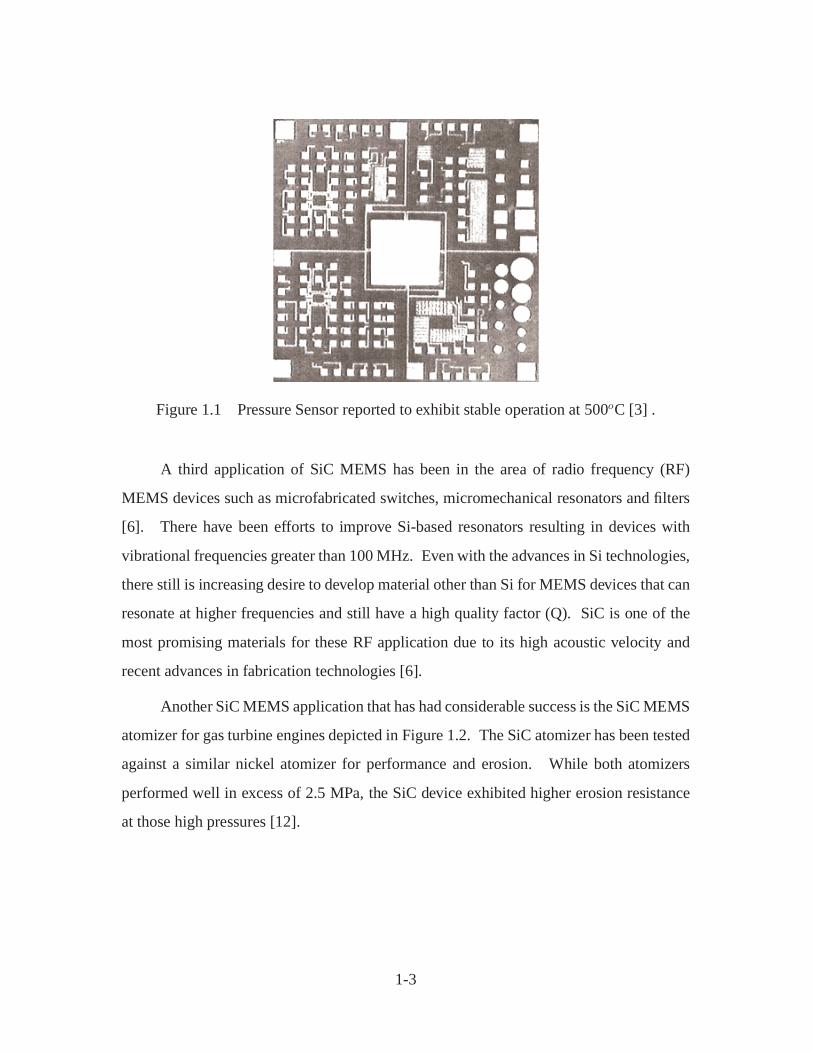
Figure 1.1 Pressure Sensor reported to exhibit stable operation at 500oC [3] .
A third application of SiC MEMS has been in the area of radio frequency (RF)
MEMS devices such as microfabricated switches, micromechanical resonators and filters
[6]. There have been efforts to improve Si-based resonators resulting in devices with
vibrational frequencies greater than 100 MHz. Even with the advances in Si technologies,
there still is increasing desire to develop material other than Si for MEMS devices that can
resonate at higher frequencies and still have a high quality factor (Q). SiC is one of the
most promising materials for these RF application due to its high acoustic velocity and
recent advances in fabrication technologies [6].
Another SiC MEMS application that has had considerable success is the SiC MEMS
atomizer for gas turbine engines depicted in Figure 1.2. The SiC atomizer has been tested
against a similar nickel atomizer for performance and erosion. While both atomizers
performed well in excess of 2.5 MPa, the SiC device exhibited higher erosion resistance
at those high pressures [12].
1-3
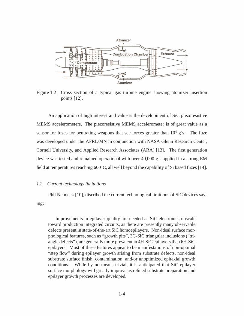
Figure 1.2 Cross section of a typical gas turbine engine showing atomizer insertionpoints [12].
An application of high interest and value is the development of SiC piezoresistive
MEMS accelerometers. The piezoresistive MEMS accelerometer is of great value as a
sensor for fuzes for pentrating weapons that see forces greater than 104 g’s. The fuze
was developed under the AFRL/MN in conjunction with NASA Glenn Research Center,
Cornell University, and Applied Research Associates (ARA) [13]. The first generation
device was tested and remained operational with over 40,000-g’s applied in a strong EM
field at temperatures reaching 600oC, all well beyond the capability of Si based fuzes [14].
1.2 Current technology limitations
Phil Neudeck [10], discribed the current technological limitions of SiC devices say-
ing:
Improvements in epilayer quality are needed as SiC electronics upscaletoward production integrated circuits, as there are presently many observabledefects present in state-of-the-art SiC homoepilayers. Non-ideal surface mor-phological features, such as “growth pits”, 3C-SiC triangular inclusions (“tri-angle defects”), are generally more prevalent in 4H-SiC epilayers than 6H-SiCepilayers. Most of these features appear to be manifestations of non-optimal“step flow” during epilayer growth arising from substrate defects, non-idealsubstrate surface finish, contamination, and/or unoptimized epitaxial growthconditions. While by no means trivial, it is anticipated that SiC epilayersurface morphology will greatly improve as refined substrate preparation andepilayer growth processes are developed.
1-4
In a 2002 IEEE paper, "Silicon Carbide for MEMS and NEMS-An Overview" the
authors C. Zorman and M. Mehrgany [5] from Case Western University, outline the state-
of-the-art fabrication techniques for SiC MEMS. In that paper, they stated some of the
limitations that fabricators are experiencing, saying:
Despite the initial success in fabricating devices using the multilayer mi-cromolding process, several technical issues must be addressed before theprocess is at the level of poly-Si surface micromachining. In terms of resid-ual stress, the measured values for the atmospheric pressure chemical vapordeposition (APCVD) poly-SiC films was not unreasonably high (140MPa).However, the films suffered from excessive stress gradients, which leads tosignificant bending of beams, especially for long, narrow structures. Suchbending had harmful effects on comb-drive actuators and other devices thatrequire coplanar structures [5].
1.3 Problem Statement and Research Objectives
The objective of this research is to determine a non-destructive evaluation (NDE)
method of identifying residual stress, stress gradients and defects in SiC MEMS. A corre-
lation between variations the Raman spectrum of SiC and stress in the crystal structure is
to be shown. An NDE technique that employs the spatial mapping of the Raman spectrum
across SiC MEMS will allow for visual identification of areas containing residual stress
and defects.
1.4 Thesis Organization
This thesis is broken into five chapters. Chapter II contains background informa-
tion including: a description of the basics of Raman spectroscopy, the causes of residual
stress, background on SiC MEMS, general knowledge about SiC crystals, and a thorough
literature review. In Chapter III, there is a description of the SiC samples that were investi-
gated. Chapter IV contains a brief description the experimental equipment and procedures.
Chapter V presents the results of the experiments and discusses the results. In Chapter VI,
the conclusions from the results are drawn and future work is laid out.
1-5
II. Background Information
Chapter I gave an introduction to the problem being addressed by this work. This chapter
explains the background information on: (1) µ−Raman spectroscopy, (2) residual stress,
(3) the previous characterization of residual stress in Si using µ−Raman spectroscopy,
(4) basic knowledge of the material characteristics of SiC, and (5) a literature review on
important topics related to the detection of residual stress in SiC using µ−Raman spec-
troscopy.
2.1 µ−Raman Spectroscopy
µ−Raman was chosen to investigate residual stress in SiC MEMS because it is an
established technique for investigating crystal defects in SiC. According to E. Martin
et al., µ−Raman has been show capable of : "(i) micrometer size lateral resolution, (ii)
polytype identification, (iii) it is sensitive to crystal disorder, (iv) it is sensitive to stress,
and (v) it is sensitive to doping" [15].
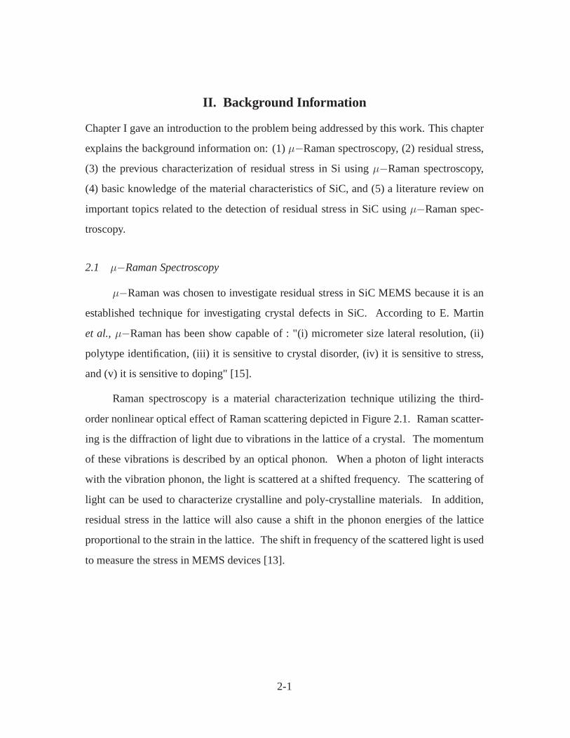
Raman spectroscopy is a material characterization technique utilizing the third-
order nonlinear optical effect of Raman scattering depicted in Figure 2.1. Raman scatter-
ing is the diffraction of light due to vibrations in the lattice of a crystal. The momentum
of these vibrations is described by an optical phonon. When a photon of light interacts
with the vibration phonon, the light is scattered at a shifted frequency. The scattering of
light can be used to characterize crystalline and poly-crystalline materials. In addition,
residual stress in the lattice will also cause a shift in the phonon energies of the lattice
proportional to the strain in the lattice. The shift in frequency of the scattered light is used
to measure the stress in MEMS devices [13].
2-1
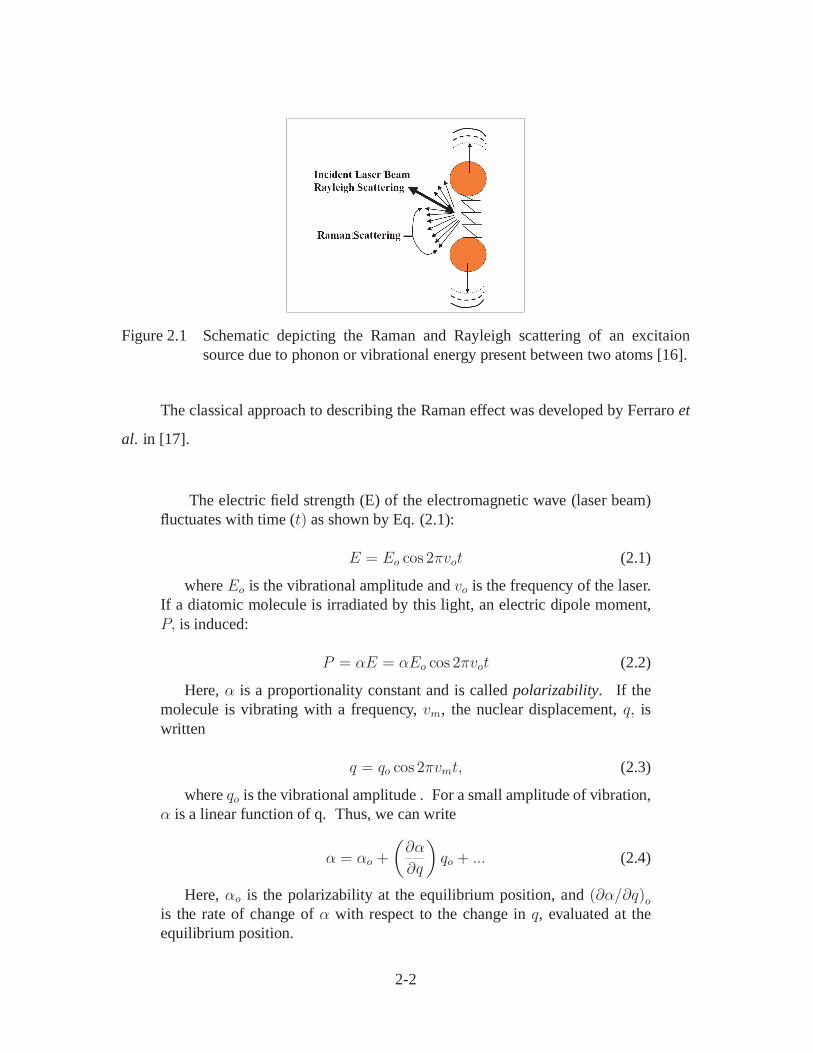
Figure 2.1 Schematic depicting the Raman and Rayleigh scattering of an excitaionsource due to phonon or vibrational energy present between two atoms [16].
The classical approach to describing the Raman effect was developed by Ferraro et
al. in [17].
The electric field strength (E) of the electromagnetic wave (laser beam)fluctuates with time (t) as shown by Eq. (2.1):
E = Eo cos 2πvot (2.1)
where Eo is the vibrational amplitude and vo is the frequency of the laser.If a diatomic molecule is irradiated by this light, an electric dipole moment,P, is induced:
P = αE = αEo cos 2πvot (2.2)
Here, α is a proportionality constant and is called polarizability. If themolecule is vibrating with a frequency, vm, the nuclear displacement, q, iswritten
q = qo cos 2πvmt, (2.3)
where qo is the vibrational amplitude . For a small amplitude of vibration,α is a linear function of q. Thus, we can write
α = αo +∂α
∂qqo + ... (2.4)
Here, αo is the polarizability at the equilibrium position, and (∂α/∂q)ois the rate of change of α with respect to the change in q, evaluated at theequilibrium position.
2-2
Combining (2.2) with (2.3) and (2.4), we obtain
P = αEo cos 2πvot
= αoEo cos 2πvot+∂α
∂q o
qEo cos 2πvot
= αoEo cos 2πvot+∂α
∂q o
qEo cos 2πvot cos 2πvmt
= αEo cos 2πvot
+1
2
∂α
∂q o
qEo [cos 2π(vo + vm)t+ cos 2π(vo − vm) · t] (2.5)
According to classical theory, the first term represents an oscillating dipolethat radiates light of frequency, vo , (Rayleigh scattering), while the secondterm corresponds to the Raman scattering of frequency, vo + vm (anti-Stokes)and vo − vm (Stokes). If (∂α/∂q)o is zero, the vibration is not Raman-active.Namely, to be Raman-active, the rate of change of polarizability (α) with thevibration must not be zero.
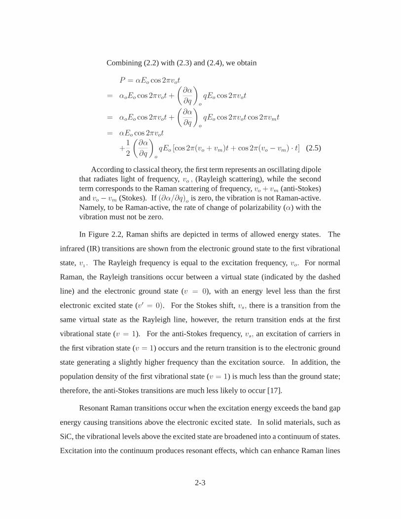
In Figure 2.2, Raman shifts are depicted in terms of allowed energy states. The
infrared (IR) transitions are shown from the electronic ground state to the first vibrational
state, v1 . The Rayleigh frequency is equal to the excitation frequency, vo. For normal
Raman, the Rayleigh transitions occur between a virtual state (indicated by the dashed
line) and the electronic ground state (v = 0), with an energy level less than the first
electronic excited state (v = 0). For the Stokes shift, vs, there is a transition from the
same virtual state as the Rayleigh line, however, the return transition ends at the first
vibrational state (v = 1). For the anti-Stokes frequency, vs, an excitation of carriers in
the first vibration state (v = 1) occurs and the return transition is to the electronic ground
state generating a slightly higher frequency than the excitation source. In addition, the
population density of the first vibrational state (v = 1) is much less than the ground state;
therefore, the anti-Stokes transitions are much less likely to occur [17].
Resonant Raman transitions occur when the excitation energy exceeds the band gap
energy causing transitions above the electronic excited state. In solid materials, such as
SiC, the vibrational levels above the excited state are broadened into a continuum of states.
Excitation into the continuum produces resonant effects, which can enhance Raman lines
2-3
by a factor of 103or 104 relative to normal Raman (see reference [17]). Fluorescence
is another effect that can occur if a carrier is excited to an electronic state. In the case
of fluorescence, an excited carrier decays to the lowest excited state (v = 0) and then
transitions to either the ground state or a vibrational level.
Figure 2.2 Energy levels for normal Raman, resonance Raman, and fluorescence spectra[17].
The 6H-SiC material used to fabricate the bulk single-crystal MEMS devices has a
unique Raman shift that has been measured in previous experiments such as the results
seen in Table 2.1. The transverse optical (TO) phonons generate three Raman shifts in
6H-SiC, TO1 at 766 cm−1and TO2 at 788 cm−1 and 796 cm−1. The longitudinal optical
(LO) phonons generate a Raman shift in 6H-SiC at 966 cm−1 [18].
2.2 Residual Stress
Residual stress is the stress that occurs in a material due to the manufacturing
process. Residual stress in 3C-SiC structures deposited on Si comes from two main
sources: differing lattice constants and different thermal expansion coefficients. Other
2-4
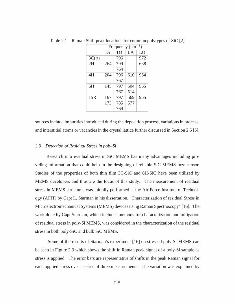
Table 2.1 Raman Shift peak locations for common polytypes of SiC [2]Frequency (cm−1)
TA TO LA LO3C(β) 796 9722H 264 799 688
7644H 204 796 610 964
7676H 145 797 504 965
767 51415R 167 797 569 965
173 785 577769
sources include impurities introduced during the deposition process, variations in process,
and interstitial atoms or vacancies in the crystal lattice further discussed in Section 2.6 [5].
2.3 Detection of Residual Stress in poly-Si
Research into residual stress in SiC MEMS has many advantages including pro-
viding information that could help in the designing of reliable SiC MEMS fuze sensor.
Studies of the properties of both thin film 3C-SiC and 6H-SiC have been utilized by
MEMS developers and thus are the focus of this study. The measurement of residual
stress in MEMS structures was initially performed at the Air Force Institute of Technol-
ogy (AFIT) by Capt L. Starman in his dissertation, “Characterization of residual Stress in
Microelectromechanical Systems (MEMS) devices using Raman Spectroscopy" [16]. The
work done by Capt Starman, which includes methods for characterization and mitigation
of residual stress in poly-Si MEMS, was considered in the characterization of the residual
stress in both poly-SiC and bulk SiC MEMS.
Some of the results of Starman’s experiment [16] on stressed poly-Si MEMS can
be seen in Figure 2.3 which shows the shift in Raman peak signal of a poly-Si sample as
stress is applied. The error bars are representative of shifts in the peak Raman signal for
each applied stress over a series of three measurements. The variation was explained by
2-5
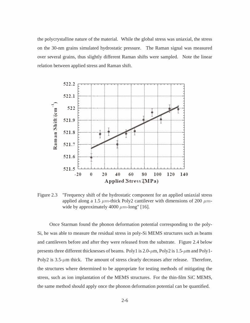
the polycrystalline nature of the material. While the global stress was uniaxial, the stress
on the 30-nm grains simulated hydrostatic pressure. The Raman signal was measured
over several grains, thus slightly different Raman shifts were sampled. Note the linear
relation between applied stress and Raman shift.
Figure 2.3 "Frequency shift of the hydrostatic component for an applied uniaxial stressapplied along a 1.5 µm-thick Poly2 cantilever with dimensions of 200 µm-wide by approximately 4000 µm-long" [16].
Once Starman found the phonon deformation potential corresponding to the poly-
Si, he was able to measure the residual stress in poly-Si MEMS structures such as beams
and cantilevers before and after they were released from the substrate. Figure 2.4 below
presents three different thicknesses of beams. Poly1 is 2.0-µm, Poly2 is 1.5-µm and Poly1-
Poly2 is 3.5-µm thick. The amount of stress clearly decreases after release. Therefore,
the structures where determined to be appropriate for testing methods of mitigating the
stress, such as ion implantation of the MEMS structures. For the thin-film SiC MEMS,
the same method should apply once the phonon deformation potential can be quantified.
2-6
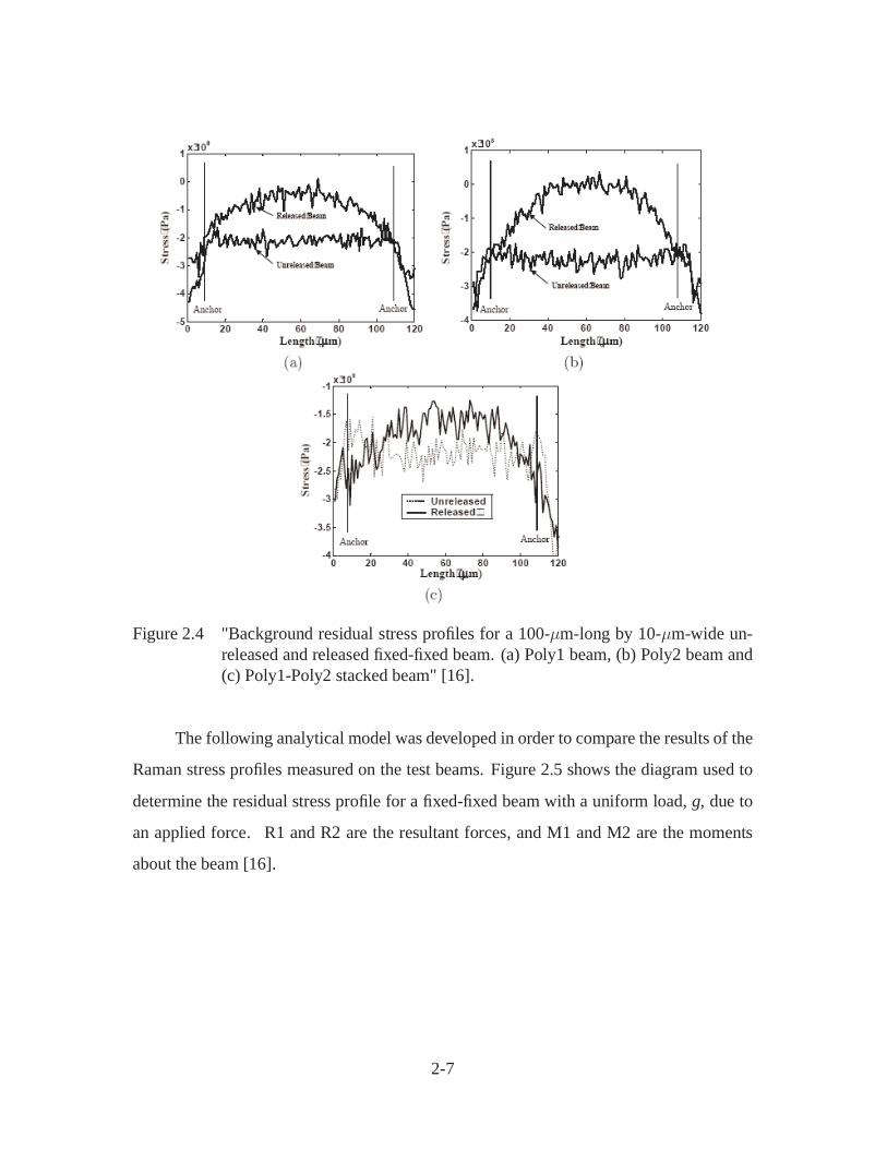
Figure 2.4 "Background residual stress profiles for a 100-µm-long by 10-µm-wide un-released and released fixed-fixed beam. (a) Poly1 beam, (b) Poly2 beam and(c) Poly1-Poly2 stacked beam" [16].
The following analytical model was developed in order to compare the results of the
Raman stress profiles measured on the test beams. Figure 2.5 shows the diagram used to
determine the residual stress profile for a fixed-fixed beam with a uniform load, g, due to
an applied force. R1 and R2 are the resultant forces, and M1 and M2 are the moments
about the beam [16].
2-7
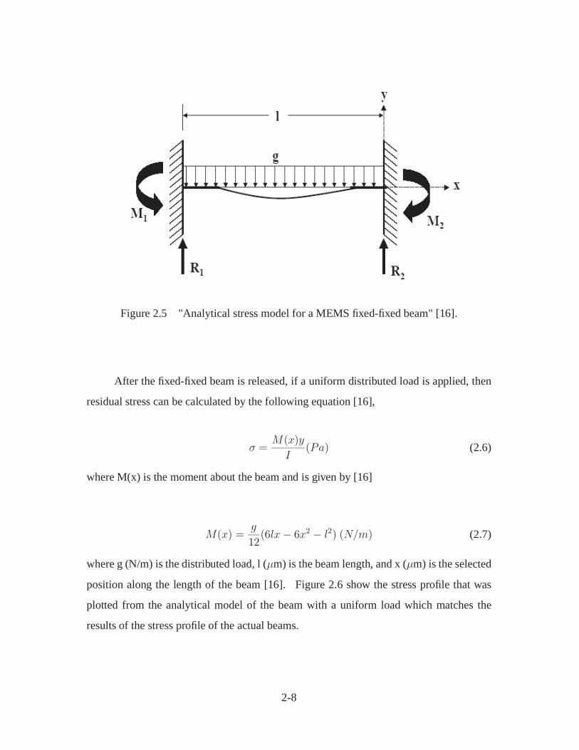
Figure 2.5 "Analytical stress model for a MEMS fixed-fixed beam" [16].
After the fixed-fixed beam is released, if a uniform distributed load is applied, then
residual stress can be calculated by the following equation [16],
σ =M(x)y
I(Pa) (2.6)
where M(x) is the moment about the beam and is given by [16]
M(x) =g
12(6lx− 6x2 − l2) (N/m) (2.7)
where g (N/m) is the distributed load, l (µm) is the beam length, and x (µm) is the selected
position along the length of the beam [16]. Figure 2.6 show the stress profile that was
plotted from the analytical model of the beam with a uniform load which matches the
results of the stress profile of the actual beams.
2-8

Figure 2.6 "Analytical stress profile of a fixed-fixed beam with a uniform load [16]."
2.4 Background Information on SiC
In order to understand SiC as a material for microdevices, it is necessary to study
the properties of SiC. SiC possesses one-dimensional polymorphism which is known as
polytypism. The different polytypes of SiC have the same planar arrangement of Si and C
atoms. The only difference in the polytypes is in the stacking arrangement of the identical
planes along either the <111> or <0001> crystal axes. These different arrangements
result in more than 250 SiC polytypes. Even though there are 250+ polytypes, there are
only three crystalline structures: cubic, hexagonal, and rhombohedral. In the past, the
cubic phase of SiC was called beta-SiC, and the hexagonal and rhombohedral structures
were called alpha-SiC. The modern, more descriptive nomenclature has been adopted
that identifies both the crystalline symmetry and stacking periodicity (C = cubic, H =
hexigonal, and R = rhombdahedral). Using this system, beta-SiC is called 3C-SiC. 3C-
SiC is the only cubic polytype known to exist. The most common alpha-SiC polytypes
have hexagonal symmetries and are called 6H-SiC, 4H-SiC, and 2H-SiC [5] (see Figure
2.7).
2-9
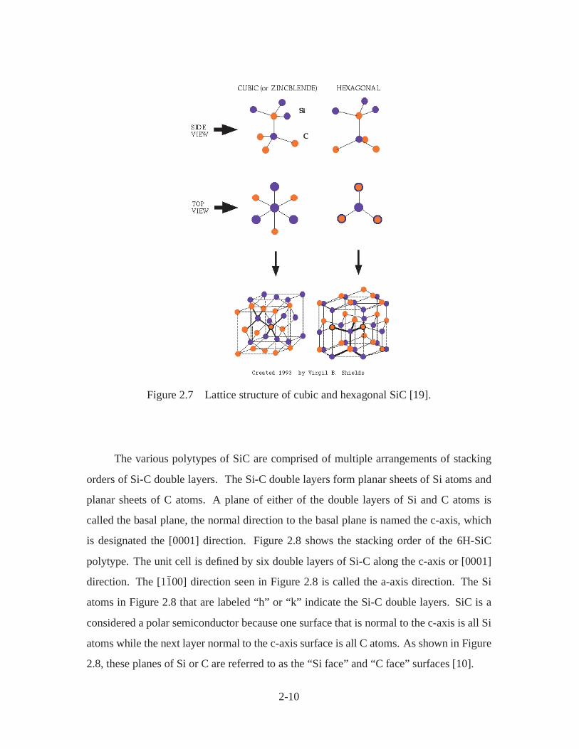
Figure 2.7 Lattice structure of cubic and hexagonal SiC [19].
The various polytypes of SiC are comprised of multiple arrangements of stacking
orders of Si-C double layers. The Si-C double layers form planar sheets of Si atoms and
planar sheets of C atoms. A plane of either of the double layers of Si and C atoms is
called the basal plane, the normal direction to the basal plane is named the c-axis, which
is designated the [0001] direction. Figure 2.8 shows the stacking order of the 6H-SiC
polytype. The unit cell is defined by six double layers of Si-C along the c-axis or [0001]
direction. The [1100] direction seen in Figure 2.8 is called the a-axis direction. The Si
atoms in Figure 2.8 that are labeled “h” or “k” indicate the Si-C double layers. SiC is a
considered a polar semiconductor because one surface that is normal to the c-axis is all Si
atoms while the next layer normal to the c-axis surface is all C atoms. As shown in Figure
2.8, these planes of Si or C are referred to as the “Si face” and “C face” surfaces [10].
2-10
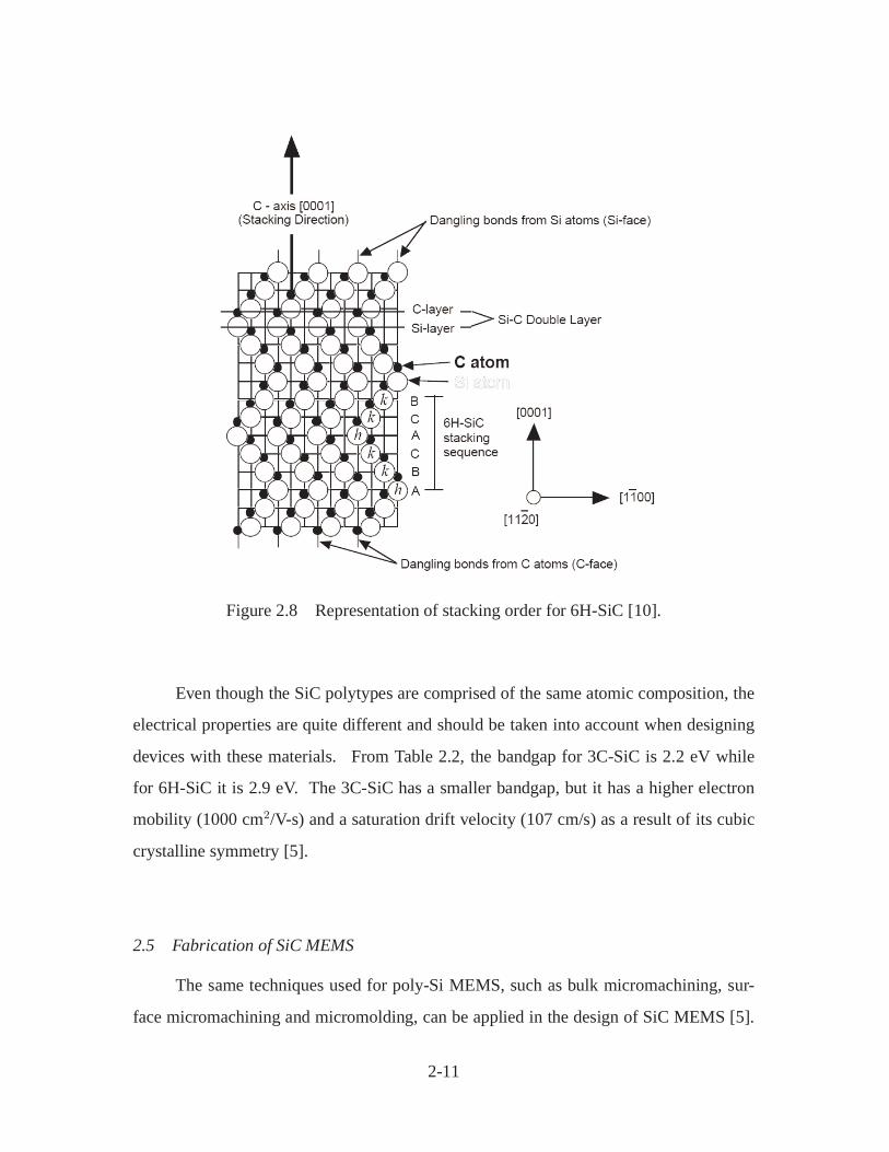
Figure 2.8 Representation of stacking order for 6H-SiC [10].
Even though the SiC polytypes are comprised of the same atomic composition, the
electrical properties are quite different and should be taken into account when designing
devices with these materials. From Table 2.2, the bandgap for 3C-SiC is 2.2 eV while
for 6H-SiC it is 2.9 eV. The 3C-SiC has a smaller bandgap, but it has a higher electron
mobility (1000 cm2/V-s) and a saturation drift velocity (107 cm/s) as a result of its cubic
crystalline symmetry [5].
2.5 Fabrication of SiC MEMS
The same techniques used for poly-Si MEMS, such as bulk micromachining, sur-
face micromachining and micromolding, can be applied in the design of SiC MEMS [5].
2-11

Table 2.2 Material Properties of 3C and 6H SiC at 300K [3]Property 3C-SiC 6H-SiC SiMelting Point (C) 1825(sublimes) 1825(sublimes) 1414Max. Operating Temp. (C) 873 1240 300Thermal Conductivity (C) 4.9 4.9 1.5Thermal Expansion Coeff. (*10−6 C−1) 3.8 4.2 2.6Young’s Modulus (GPa) 448 448 190Physical Stability Excellent Excellent GoodEnergy Gap (eV) 2.2 2.9 1.12Electron Mobility (cm2/V − s) 1000 500 1350Hole Mobility (cm2/V − s) 40 50 600Sat. Electron Drift Vel (*107 cm/s) 2.5 2 1Breakdown Voltage (*107 cm/s) 3 4-6 .3Dielectric Constant 9.7 13.2 11.9Lattice Constant (Å) 4.36 5.65 5.43
One such process that has been developed is known as the Multi-User Silicon Carbide
(MUSIC) process, which combines micromolding and micromachining techniques. The
MUSiC process is very similar to the Multi-User MEMS Processes (MUMPs) process
often used for micromachining poly-Si [5].
Bulk micromachining of SiC structures is normally done on 3C-SiC films on Si
substrates using Si bulk micromachining techniques. The technique is described as rel-
atively easy due to the chemical stability of SiC against Si anisotropic wet enchants like
KOH. However, for bulk micromachining of bulk SiC, no current anisotropic wet-etch
techniques have been identified [5].
With the limitations of bulk micromachining, SiC researchers have turned to micro-
molding techniques of poly-SiC to produce the same structures produced in Si MEMS.
Si molds are formed using deep reactive ion etching (DRIE), then coated with a thick
poly-SiC film deposited by chemical vapor deposition (CVD). The surface is then me-
chanically polished to remove the layer of poly-SiC exposing the Si mold. To release the
poly-SiC structure, the Si mold is chemically etched [5].
2-12
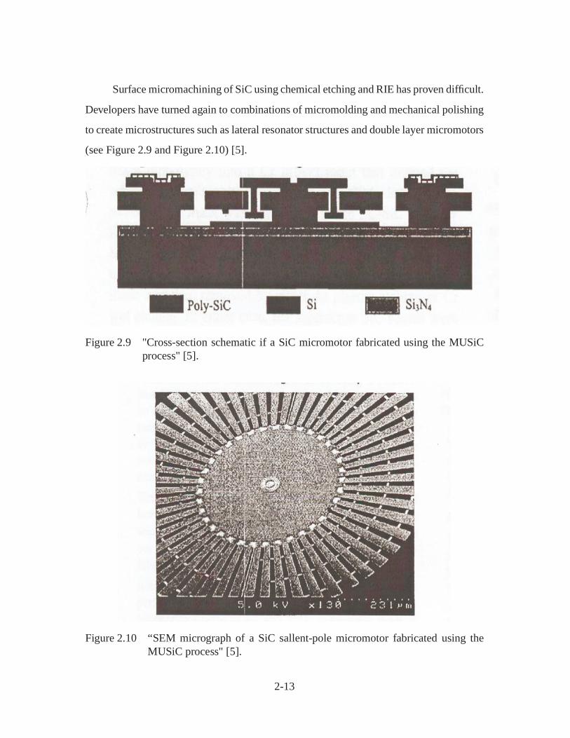
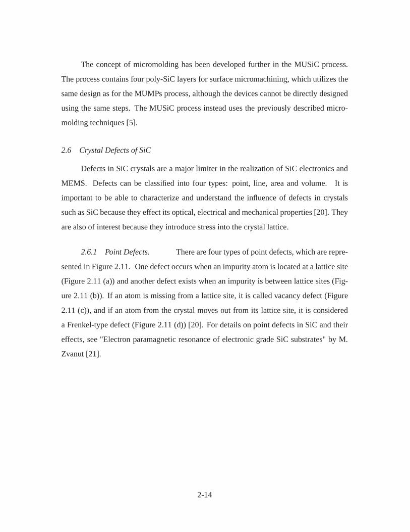
Surface micromachining of SiC using chemical etching and RIE has proven difficult.
Developers have turned again to combinations of micromolding and mechanical polishing
to create microstructures such as lateral resonator structures and double layer micromotors
(see Figure 2.9 and Figure 2.10) [5].
Figure 2.9 "Cross-section schematic if a SiC micromotor fabricated using the MUSiCprocess" [5].
Figure 2.10 “SEM micrograph of a SiC sallent-pole micromotor fabricated using theMUSiC process" [5].
2-13
The concept of micromolding has been developed further in the MUSiC process.
The process contains four poly-SiC layers for surface micromachining, which utilizes the
same design as for the MUMPs process, although the devices cannot be directly designed
using the same steps. The MUSiC process instead uses the previously described micro-
molding techniques [5].
2.6 Crystal Defects of SiC
Defects in SiC crystals are a major limiter in the realization of SiC electronics and
MEMS. Defects can be classified into four types: point, line, area and volume. It is
important to be able to characterize and understand the influence of defects in crystals
such as SiC because they effect its optical, electrical and mechanical properties [20]. They
are also of interest because they introduce stress into the crystal lattice.
2.6.1 Point Defects. There are four types of point defects, which are repre-
sented in Figure 2.11. One defect occurs when an impurity atom is located at a lattice site
(Figure 2.11 (a)) and another defect exists when an impurity is between lattice sites (Fig-
ure 2.11 (b)). If an atom is missing from a lattice site, it is called vacancy defect (Figure
2.11 (c)), and if an atom from the crystal moves out from its lattice site, it is considered
a Frenkel-type defect (Figure 2.11 (d)) [20]. For details on point defects in SiC and their
effects, see "Electron paramagnetic resonance of electronic grade SiC substrates" by M.
Zvanut [21].
2-14
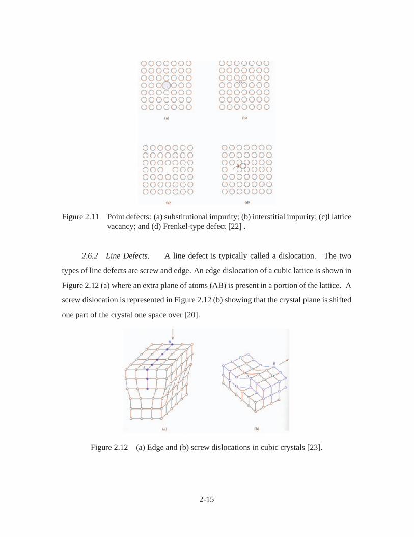
Figure 2.11 Point defects: (a) substitutional impurity; (b) interstitial impurity; (c)l latticevacancy; and (d) Frenkel-type defect [22] .
2.6.2 Line Defects. A line defect is typically called a dislocation. The two
types of line defects are screw and edge. An edge dislocation of a cubic lattice is shown in
Figure 2.12 (a) where an extra plane of atoms (AB) is present in a portion of the lattice. A
screw dislocation is represented in Figure 2.12 (b) showing that the crystal plane is shifted
one part of the crystal one space over [20].
Figure 2.12 (a) Edge and (b) screw dislocations in cubic crystals [23].
2-15
2.6.3 Area Defects. Area defects are large areas of the crystal which are discon-
tinuous. Grain bounderies such as the ones in polycrystalline material can be considered
defects. Another defect which will be considered in the results of this thesis are stacking
faults in which the stacking periodicity of the atom planes changed. If a plane is missing,
it is called an intrinsic stacking fault. If an extra plane is present, it is called an extrinsic
stacking fault [20].
Figure 2.13 Stacking faults in semiconductors: (a) intrinsic stacking fault; and (b) ex-trinsic stacking fault [22].
2.6.4 Volume Defects. Volume defects are formed from precipitants from im-
purities. When the crystal is formed, there exists a maximum concentration of impurities
that the crystal can allow. The impurities that exceed this level of concentration precipitate
and form the volume defects [20].
2.6.5 Micropipes. Micropipes are screw dislocations with a hollow core
which form hexagonal tube-like cavities that have diameters in the neighborhood of a few
µm, and form parallel to the c-axis of the hexagonal structure [24]. Most SiC experts
agree that micropipes are the most harmful defect in SiC. An image of an etched mi-
cropipe is shown in Figure 2.14. Under the current growth techniques used to produce
4H- and 6H-SiC wafers, there exist high densities of screw dislocations defects which,
like micropipes, cause a considerable amount of localized strain in the SiC. The strain will
effect the operation of both SiC MEMS and electronics [10].
2-16

Figure 2.14 Etched micropipe in a SiC diaphragm [8].
2.7 Literature Review
There has been an on going effort in the materials research community to correlate
the Raman spectrum of SiC to defects and stress in the SiC. Initial studies into the Raman
spectrum of 6H-SiC using laser excitation sources date back to 1968 with Feldman et
al. [25]. Since that time, many advances have been made in 6H-SiC crystal quality and
Raman spectrum techniques. The Raman spectrum for 6H-SiC is well characterized and
the peaks are shown in Figure 2.15 for a comparison to the Raman spectrum collected in
this research. The folded transverse optical (FTO) lines are x = 1 at 766-cm−1, x = 1/3 at
788-cm−1, and x = 0 at 796-cm−1. The folded longitudinal optical (FLO) line is for x = 0
at 966-cm−1 [18].
Where according to Feldman et al.:
For long-wavelength phonons we need to consider only the axial direc-tion of the large zone. (SiC polytype structures are characterized by a one-dimensional stacking sequence of planes. Consequently, the large zone isextended in only one direction, the axial direction, and all long wavelength
2-17
modes are found on the large-zone axis.) The standard large zone for 6H-SiCextends to 6π/c, where c is the axial dimension of the unit cell. Since 2π/cis a reciprocal lattice vector, the pseudomomentum vectors q = 0, 2π/c, 4π/c,and 6π/c are all equivalent to q = 0 in the Brillouin zone. Thus, if we definea reduced momentum x = q/qmax, the values of x accessible to Raman scattermeasurements are x = 0, 0.33, and 1 [25].
Raman spectroscopy can only detect the fundamental modes of vibration that are at
the center of the Brillouin zone where the momentum vector is k = 0. For that reason,
only the fundamental modes of vibration that occur at x = 0, 0.33 and 1 can be measured
by using Raman techniques [17]. For convenience, the intense lines at 766-cm−1,788-
cm−1and 966-cm−1 will be called TO1, TO2 and LO, respectively.
Figure 2.15 Raman Spectrum of 6H-SiC using 266-nm and 488-nm excitation sources[26].
According to Ferrero et al. [27], Figure 2.16 represents the Raman spectrum for
both 3C-SiC and 4H-SiC. The Raman peaks for the 4H-SiC were observed at 776 cm−1
for the FTO mode and at 964 cm−1 for the FLO mode. The Raman peaks for the 3C-SiC
were observed at 796 cm−1 for the FTO mode and 972 cm−1 for the FLO mode.
2-18
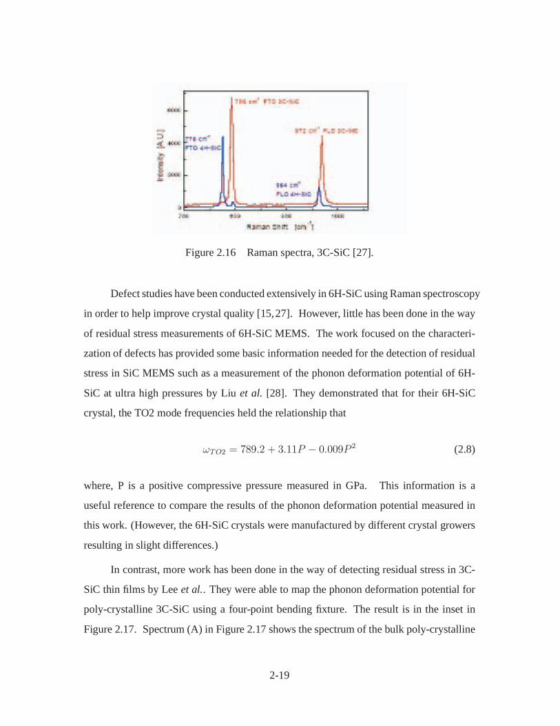
Figure 2.16 Raman spectra, 3C-SiC [27].
Defect studies have been conducted extensively in 6H-SiC using Raman spectroscopy
in order to help improve crystal quality [15,27]. However, little has been done in the way
of residual stress measurements of 6H-SiC MEMS. The work focused on the characteri-
zation of defects has provided some basic information needed for the detection of residual
stress in SiC MEMS such as a measurement of the phonon deformation potential of 6H-
SiC at ultra high pressures by Liu et al. [28]. They demonstrated that for their 6H-SiC
crystal, the TO2 mode frequencies held the relationship that
ωTO2 = 789.2 + 3.11P − 0.009P 2 (2.8)
where, P is a positive compressive pressure measured in GPa. This information is a
useful reference to compare the results of the phonon deformation potential measured in
this work. (However, the 6H-SiC crystals were manufactured by different crystal growers
resulting in slight differences.)
In contrast, more work has been done in the way of detecting residual stress in 3C-
SiC thin films by Lee et al.. They were able to map the phonon deformation potential for
poly-crystalline 3C-SiC using a four-point bending fixture. The result is in the inset in
Figure 2.17. Spectrum (A) in Figure 2.17 shows the spectrum of the bulk poly-crystalline
2-19
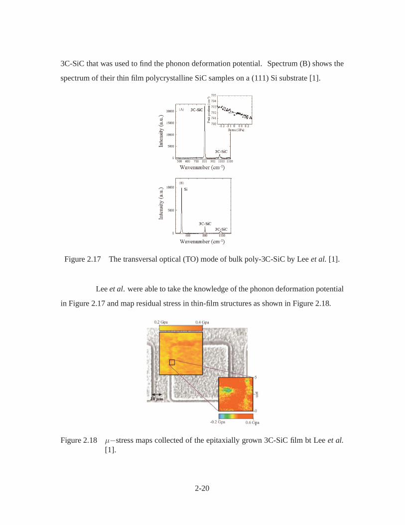
3C-SiC that was used to find the phonon deformation potential. Spectrum (B) shows the
spectrum of their thin film polycrystalline SiC samples on a (111) Si substrate [1].
Figure 2.17 The transversal optical (TO) mode of bulk poly-3C-SiC by Lee et al. [1].
Lee et al. were able to take the knowledge of the phonon deformation potential
in Figure 2.17 and map residual stress in thin-film structures as shown in Figure 2.18.
Figure 2.18 µ−stress maps collected of the epitaxially grown 3C-SiC film bt Lee et al.[1].
2-20
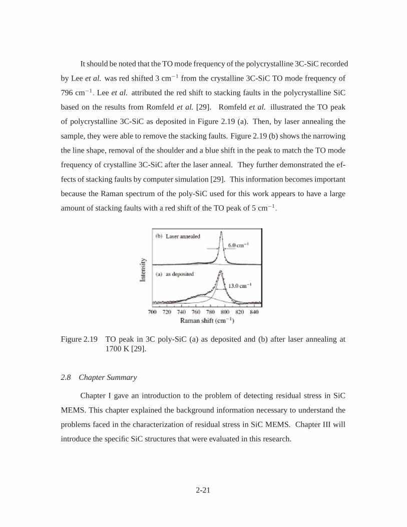
It should be noted that the TO mode frequency of the polycrystalline 3C-SiC recorded
by Lee et al. was red shifted 3 cm−1 from the crystalline 3C-SiC TO mode frequency of
796 cm−1. Lee et al. attributed the red shift to stacking faults in the polycrystalline SiC
based on the results from Romfeld et al. [29]. Romfeld et al. illustrated the TO peak
of polycrystalline 3C-SiC as deposited in Figure 2.19 (a). Then, by laser annealing the
sample, they were able to remove the stacking faults. Figure 2.19 (b) shows the narrowing
the line shape, removal of the shoulder and a blue shift in the peak to match the TO mode
frequency of crystalline 3C-SiC after the laser anneal. They further demonstrated the ef-
fects of stacking faults by computer simulation [29]. This information becomes important
because the Raman spectrum of the poly-SiC used for this work appears to have a large
amount of stacking faults with a red shift of the TO peak of 5 cm−1.
Figure 2.19 TO peak in 3C poly-SiC (a) as deposited and (b) after laser annealing at1700 K [29].
2.8 Chapter Summary
Chapter I gave an introduction to the problem of detecting residual stress in SiC
MEMS. This chapter explained the background information necessary to understand the
problems faced in the characterization of residual stress in SiC MEMS. Chapter III will
introduce the specific SiC structures that were evaluated in this research.
2-21
III. Samples
The introduction discussed the objective of this research, which is the detection of residual
stress in SiC MEMS. A review of the history and characteristics of SiC MEMS was also
covered. In this chapter, the materials that were investigated in this research are described.
The samples evaluated were fabricated from two different polytypes of SiC. The first
set of samples were MEMS fabricated from 6H-SiC and the second were thin films of
polycrystalline 3C-SiC deposited on (100) Si substrates (referred to as poly-SiC). This
chapter describes the structure of the samples.
3.1 NASA crystalline 6H-SiC accelerometer and pressure sensor
The NASA MEMS pressure sensors are described in detail to provide enough back-
ground to appreciate and understand the results of the experimental analysis. For a com-
plete description of the device function see references [8, 30].
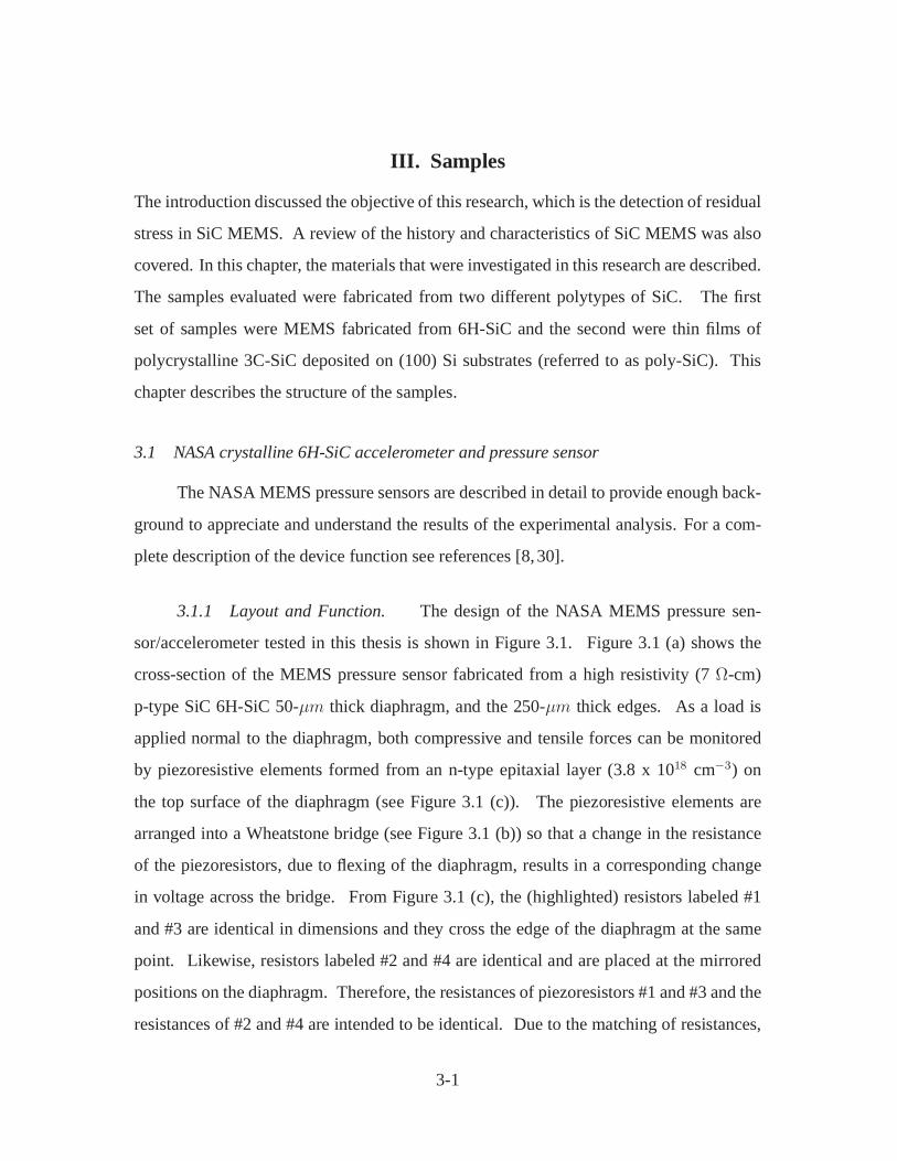
3.1.1 Layout and Function. The design of the NASA MEMS pressure sen-
sor/accelerometer tested in this thesis is shown in Figure 3.1. Figure 3.1 (a) shows the
cross-section of the MEMS pressure sensor fabricated from a high resistivity (7 Ω-cm)
p-type SiC 6H-SiC 50-µm thick diaphragm, and the 250-µm thick edges. As a load is
applied normal to the diaphragm, both compressive and tensile forces can be monitored
by piezoresistive elements formed from an n-type epitaxial layer (3.8 x 1018 cm−3) on
the top surface of the diaphragm (see Figure 3.1 (c)). The piezoresistive elements are
arranged into a Wheatstone bridge (see Figure 3.1 (b)) so that a change in the resistance
of the piezoresistors, due to flexing of the diaphragm, results in a corresponding change
in voltage across the bridge. From Figure 3.1 (c), the (highlighted) resistors labeled #1
and #3 are identical in dimensions and they cross the edge of the diaphragm at the same
point. Likewise, resistors labeled #2 and #4 are identical and are placed at the mirrored
positions on the diaphragm. Therefore, the resistances of piezoresistors #1 and #3 and the
resistances of #2 and #4 are intended to be identical. Due to the matching of resistances,
3-1
an enhancement of the output of the Wheatstone bridge should occur. In Figure 3.1 (c),
the diaphragm is apparent in the optical micrograph as a dark circle, due to the material’s
transparency. The rectangular dark regions that the resistive elements are connected to are
metal contacts. The device is packaged and the carrier leads are wire bonded to the metal
contacts [31]. There are two different devices that are tested: one with a diaphragm radius
of 650 µm, and an other with a diaphram radius of 550 µm.
Figure 3.1 (a) Cross-section of 6H-SiC MEMS diaphragm indicating points of stressfrom a shock. (b) Layout of the resistive elements forming a Wheatstonebridge. (c) Top view of the NASA 600 sample with highlights over thepiezoresistive elements [31].
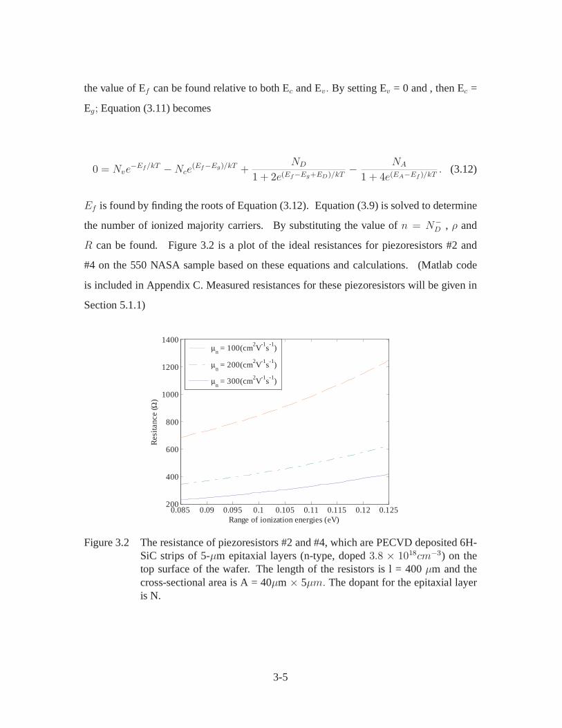
3.1.2 Resistivity of the piezoresistors #2 and #4 . The 6H-SiC structures are bulk
micro-machined by back-etching a 250-µm thick single-crystal 6H-SiC wafer (p-type, 7
Ω-cm) that includes a plasma enhanced chemical vapor deposition (PECVD) deposited
6H-SiC 5-µm epitaxial film ("epi-layer") (n-type, doped 3.8 x 1018 cm−3) on the top sur-
face of the wafer. The length of the piezoresistors #2 and #4 is 400 µm and the cross-
sectional area is 40 µm× 5 µm. The dopant for the epitaxial layer is nitrogen (N) [32]. N
3-2

is a shallow donor in 6H-SiC with ionization energies that have been measured between
0.085 and 0.125 eV [33].
According to Sze [20], the resistivity for an n-type semiconductor is defined as
ρ =1
qnµn(3.1)
where µn is electron Hall mobility in (cm2V −1s−1), q is the elementary charge, 1.602 ×10⁻¹⁹C, and n is the electron or majority carrier concentration (cm−3). The resistance, R,
of an element of length, l, and area, A, is
R = ρl
A=
1
Aqnµn. (3.2)
With a donor dopant level ND = 3 × 1018cm−3 at T = 300K, the electron Hall
mobility is µn ≈ 100 − 300(cm2V −1s−1) (see Figure A.1). Since the donor ionization
energies are greater than 3 kT,where k is Boltzman’s constant, 1.38 × 10⁻²³ JK, and T is
temprature (K), away from the conduction band (i.e., 0.085 eV > 3 kT = 0.075 eV ), the
dopants will not be fully ionized.
To determine the number of ionized majority carriers, the following equation from
Wolf et al. [34] must be balanced since
n+N−A = p +N
+D (3.3)
where p is the hole or minority carrier concentration (cm−3), n is the electron or majority
carrier concentration, N−A is the number of fully ionized acceptors, andN+
D is the number
of fully ionized donors. From Sze [20],
n = Nce−(EC−EF )/kT (3.4)
and
3-3

p = Nve−(Ef−Ev)/kT , (3.5)
whereNc is the density of states in the conduction band (cm−3),Nv is the density of states
in the valence band, Ef is the Fermi energy level (eV), Ev is the energy of top the edge
of the valance band, Ec is the energy of the bottom edge of the conduction band. From
Levinshtein et al. [33],
Nc ∼= 1.73× 10¹⁶ × T 3/2(cm−3) (3.6)
and
Nv ∼= 4.8× 10¹⁵ × T 3/2(cm−3). (3.7)
The number of ionized dopants are found by [34]
N−A =
NA1 + 4e(EA−Ef )/kT
(3.8)
and
N+D =
ND1 + 2e(Ef−ED)/kT
. (3.9)
Finally, the Varshney equation, which gives the energy gap as a function of lattice tempra-
ture, for 6H-SiC is [33]
Eg = Eg(0)− 6.5× 10⁻⁴ × T 2
T + 1200(eV ). (3.10)
By substituting (3.4)-(3.9) into (3.3) [35]:
0 = Nve−(Ef−Ev)/kT −Nce−(EC−Ef )/kT + ND
1 + 2e(Ef−ED)/kT− NA1 + 4e(EA−Ef )/kT
, (3.11)
3-4
the value of Ef can be found relative to both Ec and Ev. By setting Ev = 0 and , then Ec =
Eg; Equation (3.11) becomes
0 = Nve−Ef/kT −Nce(Ef−Eg)/kT + ND
1 + 2e(Ef−Eg+ED)/kT− NA1 + 4e(EA−Ef )/kT
. (3.12)
Ef is found by finding the roots of Equation (3.12). Equation (3.9) is solved to determine
the number of ionized majority carriers. By substituting the value of n = N−D , ρ and
R can be found. Figure 3.2 is a plot of the ideal resistances for piezoresistors #2 and
#4 on the 550 NASA sample based on these equations and calculations. (Matlab code
is included in Appendix C. Measured resistances for these piezoresistors will be given in
Section 5.1.1)
0.085 0.09 0.095 0.1 0.105 0.11 0.115 0.12 0.125200
400
600
800
1000
1200
1400
Range of ionization energies (eV)
Res
itan
ce (Ω
)
µn = 100(cm2V
-1s
-1)
µn = 200(cm2V-1s-1)
µn = 300(cm2V-1s-1)
Figure 3.2 The resistance of piezoresistors #2 and #4, which are PECVD deposited 6H-SiC strips of 5-µm epitaxial layers (n-type, doped 3.8 × 1018cm−3) on thetop surface of the wafer. The length of the resistors is l = 400 µm and thecross-sectional area is A = 40µm × 5µm. The dopant for the epitaxial layeris N.
3-5
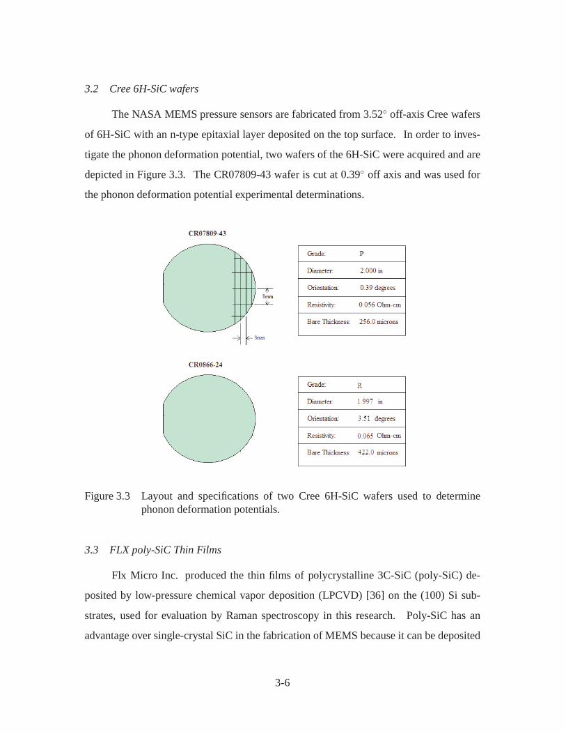
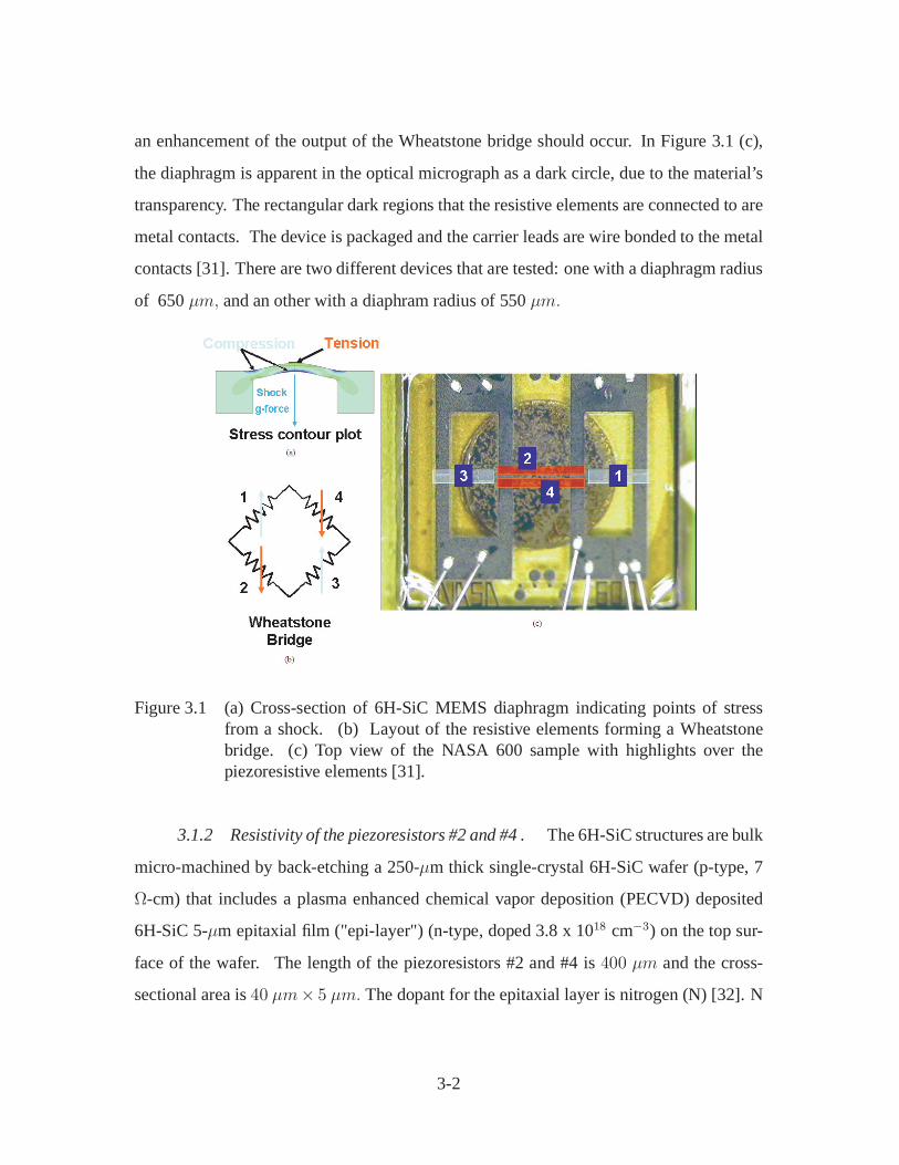
3.2 Cree 6H-SiC wafers
The NASA MEMS pressure sensors are fabricated from 3.52 off-axis Cree wafers
of 6H-SiC with an n-type epitaxial layer deposited on the top surface. In order to inves-
tigate the phonon deformation potential, two wafers of the 6H-SiC were acquired and are
depicted in Figure 3.3. The CR07809-43 wafer is cut at 0.39 off axis and was used for
the phonon deformation potential experimental determinations.
Figure 3.3 Layout and specifications of two Cree 6H-SiC wafers used to determinephonon deformation potentials.
3.3 FLX poly-SiC Thin Films
Flx Micro Inc. produced the thin films of polycrystalline 3C-SiC (poly-SiC) de-
posited by low-pressure chemical vapor deposition (LPCVD) [36] on the (100) Si sub-
strates, used for evaluation by Raman spectroscopy in this research. Poly-SiC has an
advantage over single-crystal SiC in the fabrication of MEMS because it can be deposited
3-6

on a sacrificial layer of Si dioxide (SiO2) or an electrically insulating layer of Si Nitride
(Si3N4) film [6]. Thus, the interest in measuring the Raman Shift for the characterization
of stresses in poly-SiC for MEMS structures was of interest here.
3.3.1 1.5-µm SiC on Si. A schematic cross-section of the 1.5-µm poly-SiC on
Si substrate is illustrated in Figure 3.4 (a). In Figure 3.4 (b), an optical micrograph was
taken displaying a metal mask of a comb drive that was deposited on top of the poly-SiC.
The magnification is 5X and the green dot in the middle is the laser spot of a 514-nm
argon-ion laser through the confocal microscope. (For more details on the microscope
setup, see the equipment chapter on the Raman spectrometer.)
Figure 3.4 (a) Cross-section of the 1.5-µm thick poly-SiC deposited by LPCVD [36] ona Si substrate. (b) Microscope image of the top of the FLX Micro inc. 1.5-µm poly-SiC on a Si substrate. The comb drive is a metal mask depositedonto the thin film.
3.3.2 5.5-µm SiC on Si. A schematic cross-section of the 5.5-µm SiC thin
films is depicted in Figure 3.5 (a). After the films were deposited, the back side of the
wafers were anisotopically etched by potassium hydroxide (KOH), leaving a suspended
membrane of SiC. In 3.5 (b), an optical micrograph of the top surface of the 5.5-µm
thin film is shown. The membrane was fractured during transport and dropped below
the support structure (the dark shape in the middle of the picture). The picture is shown
to reveal the edge of the diaphragm. Intact samples were used for all Raman spectral
3-7
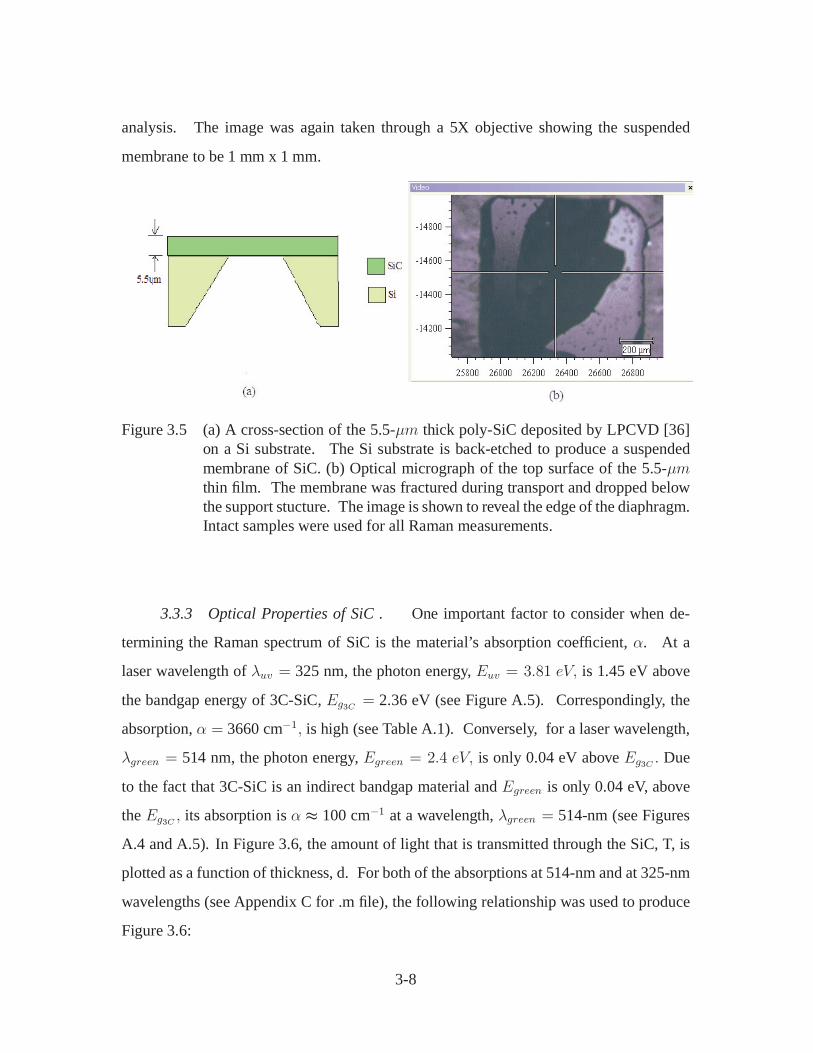
analysis. The image was again taken through a 5X objective showing the suspended
membrane to be 1 mm x 1 mm.
Figure 3.5 (a) A cross-section of the 5.5-µm thick poly-SiC deposited by LPCVD [36]on a Si substrate. The Si substrate is back-etched to produce a suspendedmembrane of SiC. (b) Optical micrograph of the top surface of the 5.5-µmthin film. The membrane was fractured during transport and dropped belowthe support stucture. The image is shown to reveal the edge of the diaphragm.Intact samples were used for all Raman measurements.
3.3.3 Optical Properties of SiC . One important factor to consider when de-
termining the Raman spectrum of SiC is the material’s absorption coefficient, α. At a
laser wavelength of λuv = 325 nm, the photon energy, Euv = 3.81 eV, is 1.45 eV above
the bandgap energy of 3C-SiC, Eg3C = 2.36 eV (see Figure A.5). Correspondingly, the
absorption, α = 3660 cm−1, is high (see Table A.1). Conversely, for a laser wavelength,
λgreen = 514 nm, the photon energy, Egreen = 2.4 eV, is only 0.04 eV above Eg3C . Due
to the fact that 3C-SiC is an indirect bandgap material and Egreen is only 0.04 eV, above
the Eg3C , its absorption is α ≈ 100 cm−1 at a wavelength, λgreen = 514-nm (see Figures
A.4 and A.5). In Figure 3.6, the amount of light that is transmitted through the SiC, T, is
plotted as a function of thickness, d. For both of the absorptions at 514-nm and at 325-nm
wavelengths (see Appendix C for .m file), the following relationship was used to produce
Figure 3.6:
3-8
10-1 100 101 102 1030
10
20
30
40
50
60
70
80
90
100
SiC film thickness (µm)
Perc
ent
of li
ght t
rans
mite
d3C-SiC at 325nm3C-SiC at 514nm6H-SiC at 325nm6H-SiC at 514nm
Figure 3.6 Percent of light transmitted as a function of thickness of SiC by the 325 nmand 512 nm lasers for both 6H and 3C polytypes. 3C-SiC absorption val-ues come from Figures A.1 and A.4. 6H-SiC absorption values come fromFigures A.2 and A.3.
T = e−αd (3.13)
The data become important when looking at thin films by Raman spectroscopy be-
cause it gives an indication of how much light will reach the Si substrate which is highly
Raman active for many wavelengths. Also included is the absoption of 6H-SiC for both
wavelengths at λ = 514 nm, α ≈ 20 cm−1(See Figure A.3) and at λ = 325 nm, α ≈ 5 ×103 cm−1(See Figure A.2).
3.4 Chapter Summary
In this chapter, samples fabricated from two different polytypes of SiC that
were investigated were described. The first one was MEMS fabricated from 6H-SiC and
3-9

the second set of samples were thin films of polycrystalline 3C-SiC deposited on (100)
Si substrates (referred to as poly-SiC). The next chapter describes the characterization
methods used to study the samples.
3-10
IV. Equipment and Experiments
The equipment for characterization of the SiC samples described in Chapter III are intro-
duced in this section. More detailed information is available on most of the equipment
through the manufacturers. Experimental procedures are also outlined.
4.1 Probe Station
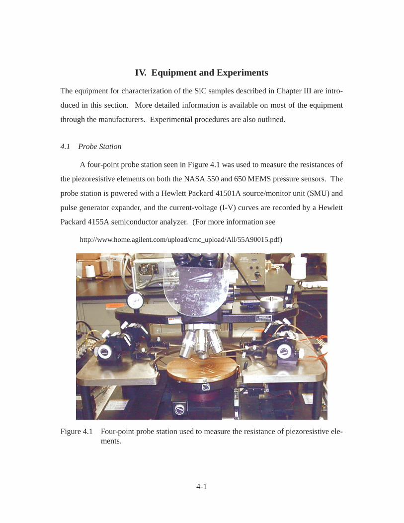
A four-point probe station seen in Figure 4.1 was used to measure the resistances of
the piezoresistive elements on both the NASA 550 and 650 MEMS pressure sensors. The
probe station is powered with a Hewlett Packard 41501A source/monitor unit (SMU) and
pulse generator expander, and the current-voltage (I-V) curves are recorded by a Hewlett
Packard 4155A semiconductor analyzer. (For more information see
http://www.home.agilent.com/upload/cmc_upload/All/55A90015.pdf)
Figure 4.1 Four-point probe station used to measure the resistance of piezoresistive ele-ments.
4-1
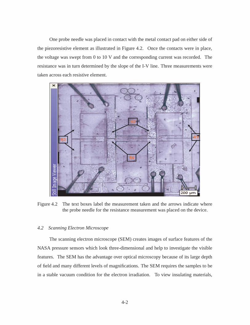
One probe needle was placed in contact with the metal contact pad on either side of
the piezoresistive element as illustrated in Figure 4.2. Once the contacts were in place,
the voltage was swept from 0 to 10 V and the corresponding current was recorded. The
resistance was in turn determined by the slope of the I-V line. Three measurements were
taken across each resistive element.
Figure 4.2 The text boxes label the measurement taken and the arrows indicate wherethe probe needle for the resistance measurement was placed on the device.
4.2 Scanning Electron Microscope
The scanning electron microscope (SEM) creates images of surface features of the
NASA pressure sensors which look three-dimensional and help to investigate the visible
features. The SEM has the advantage over optical microscopy because of its large depth
of field and many different levels of magnifications. The SEM requires the samples to be
in a stable vacuum condition for the electron irradiation. To view insulating materials,
4-2
a gold coating is needed to produce a conducting surface and to prevent electrical charge
effects. For SiC, the coating is not required because of its conduction properties [37].
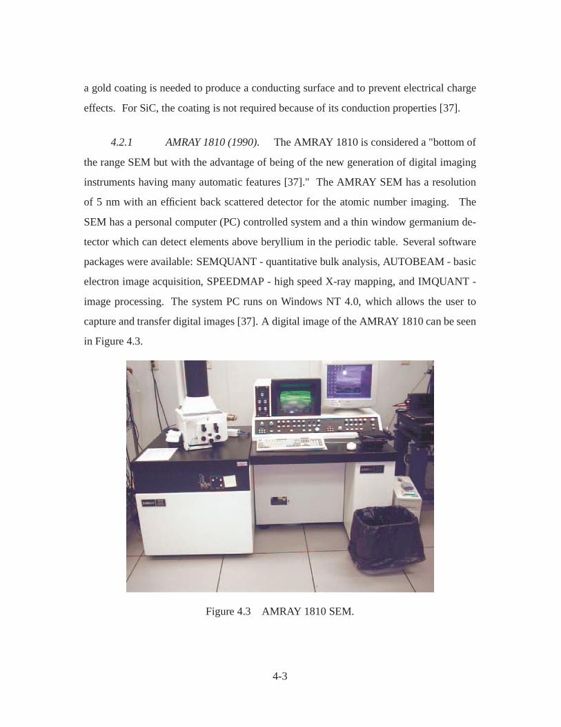
4.2.1 AMRAY 1810 (1990). The AMRAY 1810 is considered a "bottom of
the range SEM but with the advantage of being of the new generation of digital imaging
instruments having many automatic features [37]." The AMRAY SEM has a resolution
of 5 nm with an efficient back scattered detector for the atomic number imaging. The
SEM has a personal computer (PC) controlled system and a thin window germanium de-
tector which can detect elements above beryllium in the periodic table. Several software
packages were available: SEMQUANT - quantitative bulk analysis, AUTOBEAM - basic
electron image acquisition, SPEEDMAP - high speed X-ray mapping, and IMQUANT -
image processing. The system PC runs on Windows NT 4.0, which allows the user to
capture and transfer digital images [37]. A digital image of the AMRAY 1810 can be seen
in Figure 4.3.
Figure 4.3 AMRAY 1810 SEM.
4-3

4.3 Zygo Interferometer
The Zygo NewView was used to acquire three-dimensional surface structure data of
the pressure sensor for analysis. The system combines graphic images and high resolution
numerical analysis to accurately characterize the surface structure of the samples. The
NewView utilizes scanning white light interferometry in order to image and measure the
micro-structure and topography of surfaces in three dimensions [38]. A schematic of the
NewView Zygo interferometer system is shown in Figure 4.4.
Figure 4.4 Diagram of the New View Zygo interferometer system [38].
4.4 InVia Raman Spectrometer
A schematic of the InVia Raman specrometer, produced by Renishaw Inc., is shown
in Figure 4.5. The laser light enters the system and first passes through a beam expander
(labeled E) in order to collimate the light. The beam is guided through to the confocal
microscope where it is focused through by an objective onto the investigated sample (with
4-4

50X objective, the spot size is ∼1 µm in the focal plane). The samples are placed on
the piezoelectric stage in the focal plane of the microscope (labeled A). The light reflects
off the samples back through the microscope, and is passed through a notch filter (D)
to reduce the intensity of the Rayleigh line without affecting the Raman shift intensity.
The light then passes through the entrance slit (B) to the monochromator. Light reflects
off of the triangle mirror and is dispersed by a grating with a number of lines per mm
corresponding to the excitation wavelength. The dispersed light is then passed through the
50-µm exit slit onto a CCD array (F) [39].
Figure 4.5 Diagram of a Renishaw Raman spectrometer [39].
4.4.1 Spectral Resolution. The InVia Raman spectrometer is based on a single
monochromator. Therefore, the resolution of the spectrometer for the wavelengths of 325-
nm (UV) and 514-nm (green) may be calculated using the following equation:
4-5

∆λ =wa
fm, (4.1)
where w is the slit width, a is grating tooth spacing, f is the focal length of the monochro-
mator and m is the diffraction order. Examples for some of the wavelengths relevant to
this work are worked out below using the data from Renishaw.
Example 1 λ = 325nm;
∆λ = afmw = 1
200mm×2400(1/mm)50µm = 1. 041 7× 10⁻¹⁰m
∆ν = 1λ2∆λ = 1
(325nm)2× 1. 041 7× 10⁻¹⁰m = 9. 862 2cm−1
Example 2 λ = 514nm;
∆λ = afmw = 1
200mm×1800(1/mm)50µm = 1. 388 9× 10⁻¹⁰m
∆ν = 1λ2∆λ = 1
(514nm)2× 1.3889× 10−10m = 5. 257 1cm−1
Example 3 λ = 1064 nm;
∆λ = afmw = 1
200mm×1200(1/mm)50µm = 2. 083 3× 10⁻¹⁰m
∆ν = 1λ2∆λ = 1
(1064nm)2× 2. 083 3× 10⁻¹⁰m = 1. 840 2cm−1
Table 4.1 shows some of the advertised capabilities of the InVia Raman spectrometer
found on the world wide web (http://www.renishaw.com/UserFiles/acrobat/UKEnglish/SPD-
TN-014.pdf ). It should be noted that the advertised spectral resolution is only for the con-
figuration with the infrared (IR) laser, and that the laser wavelengths used for the Raman
experiments (325 nm and 514 nm) do not provide the advertised spectral resolution. Four
different lasers with the following wavelengths; 830 nm, 633 nm, 514 nm and 325 nm, are
available at AFRL/ML. Renishaw Inc. has provided a spread sheet that will calculate the
spectral resolution and other important parameters. A snap shot of the results for 514-nm
and 325-nm wavelengths can be found in the Appendix B Figures B.3 and B.2. The spec-
tral resolution computed by the Renishaw’s spread sheet closely matches the results of the
spectral resolution based on the monochromator equations above.
4-6

Table 4.1 Renishaw InVia Raman spectrometer advertised capabilities.Description Renishaw’s inVia Raman microscopeWavelength coverage ∼10 cm−1 to 9000 cm−1
Laser options multiple,from 244 nm to 830 nmDetector Si CCDNoise limitation signal shot noise limitedMicroscope spatial resolution < 1 µm (depending on configuration)Spectral resolution ∼1 cm−1(depending on configura-
tion)
4.4.2 Sampling Rate. The InVia Raman spectrometer has variable spectral reso-
lution based on the wavelength of the excitation source. Therefore, the sampling rate must
be dynamic. Raman spectra will be explained further in the results section, but Figure
4.6 (a) and (c) depict the two typical spectra. Figure 4.6 (a) is the Raman spectrum of
diamond powder, which has a main Raman peak with a line center at 1331 cm−1 relative
to the 325-nm laser line defined as 0 cm−1. Figure 4.6 (b) is a close up view of the Raman
line of the diamond powder showing only the data points collected which demonstrates
the sampling rate of the InVia Raman spectrometer using a 325-nm source to be 3 cm−1.
Figure 4.6 (c) is the Raman spectrum of 6H-SiC which has an LO Raman peak line center
at 966 cm−1 and is excited using a 514-nm laser. Figure 4.6 (d) is a close-up view of the
LO peak showing the sampling rate with a 514-nm source to be 2 cm−1.
4-7
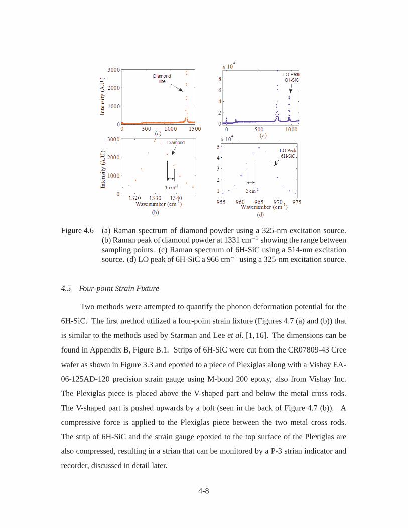
Figure 4.6 (a) Raman spectrum of diamond powder using a 325-nm excitation source.(b) Raman peak of diamond powder at 1331 cm−1 showing the range betweensampling points. (c) Raman spectrum of 6H-SiC using a 514-nm excitationsource. (d) LO peak of 6H-SiC a 966 cm−1 using a 325-nm excitation source.
4.5 Four-point Strain Fixture
Two methods were attempted to quantify the phonon deformation potential for the
6H-SiC. The first method utilized a four-point strain fixture (Figures 4.7 (a) and (b)) that
is similar to the methods used by Starman and Lee et al. [1, 16]. The dimensions can be
found in Appendix B, Figure B.1. Strips of 6H-SiC were cut from the CR07809-43 Cree
wafer as shown in Figure 3.3 and epoxied to a piece of Plexiglas along with a Vishay EA-
06-125AD-120 precision strain gauge using M-bond 200 epoxy, also from Vishay Inc.
The Plexiglas piece is placed above the V-shaped part and below the metal cross rods.
The V-shaped part is pushed upwards by a bolt (seen in the back of Figure 4.7 (b)). A
compressive force is applied to the Plexiglas piece between the two metal cross rods.
The strip of 6H-SiC and the strain gauge epoxied to the top surface of the Plexiglas are
also compressed, resulting in a strian that can be monitored by a P-3 strian indicator and
recorder, discussed in detail later.
4-8

(a) (b)(a) (b)
Figure 4.7 (a) Top view of the four-point strain fixture. (b) Sideview of the four-pointstrain fixture.
4.6 Vice
A second experimental setup to determine the phonon deformation potential of 6H-
SiC utilized a vice. A 1-cm2 sample of the CR07809-43 Cree wafer had an EA-06-
125AD-120 precision strain gauge was epoxied to the unpolished side of the sample using
M-bond 200. The sample was placed in a vice as shown in Figure 4.8. A stress was
applied directly to the crystal, and the strain on the crystal and strain gauge was monitored
by a P-3 strain indicator described in the next section. For each increment of stress applied
to the crystal, the corresponding Raman spectrum of the crystal was recorded and curve
fit to the line shape using Wire 2.0R
software to track the shift in the Raman peaks as a
function of the applied stress. Note, as the pressure was applied to the crystal the sample
slightly bucked upwards producing a tensile stress on the top surface. The buckling was
determined optically as a change in the focal plane of the microscope.
A third method for mapping the phonon deformation potential would be to use a
diamand anvil cell as reported by Liu et al. [28].
4-9
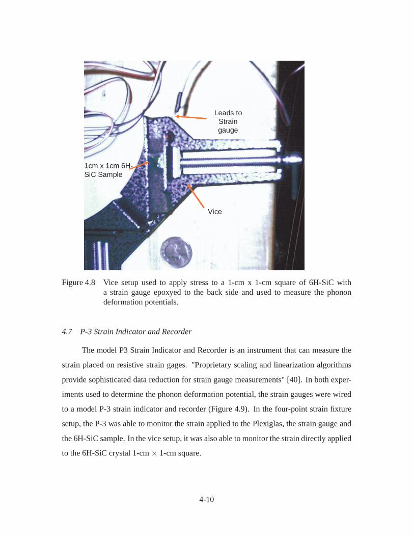
1cm x 1cm 6H-SiC Sample
Vice
Leads to Strain gauge
Figure 4.8 Vice setup used to apply stress to a 1-cm x 1-cm square of 6H-SiC witha strain gauge epoxyed to the back side and used to measure the phonondeformation potentials.
4.7 P-3 Strain Indicator and Recorder
The model P3 Strain Indicator and Recorder is an instrument that can measure the
strain placed on resistive strain gages. "Proprietary scaling and linearization algorithms
provide sophisticated data reduction for strain gauge measurements" [40]. In both exper-
iments used to determine the phonon deformation potential, the strain gauges were wired
to a model P-3 strain indicator and recorder (Figure 4.9). In the four-point strain fixture
setup, the P-3 was able to monitor the strain applied to the Plexiglas, the strain gauge and
the 6H-SiC sample. In the vice setup, it was also able to monitor the strain directly applied
to the 6H-SiC crystal 1-cm × 1-cm square.
4-10
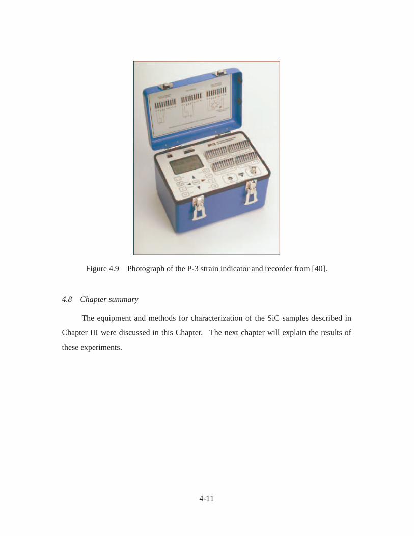
Figure 4.9 Photograph of the P-3 strain indicator and recorder from [40].
4.8 Chapter summary
The equipment and methods for characterization of the SiC samples described in
Chapter III were discussed in this Chapter. The next chapter will explain the results of
these experiments.
4-11

V. Results and Data Analysis
The previous chapters introduced the idea that µ−Raman spectroscopy can be used as
a method of detecting residual stress in SiC MEMS. The different sample materials were
described in Chapter III. This chapter presents and discusses the results of the experiments
outlined in Chapter IV.
5.1 NASA 550 and 650 6H-SiC MEMS
The investigation of the NASA MEMS samples led to promising results that are
discribed in the following sections.
5.1.1 Resistance of piezoresistors. In order to determine whether the residual
stress measured in the NASA 550 pressure sensor piezoresistors had any effect on the
balance of the Wheatstone bridge, the resistances of the piezoresistors were determined
by measuring the current-voltage (I-V) relationship using the four-point-probe station (see
Section 4.1). From the I-V information, Ohms law,
V = i×R (5.1)
was used to back out the resistances. Three measurements were recorded and averaged
across each resistor.
Table 5.1 shows the average measured resistances of the four piezoresistors on the
NASA 550 and 650 pressure sensors. In Figure 4.2, it was shown where the measurements
were taken. On each resistor the resistace was measured three times and the standard
deviation was computed using the following spread sheet function
(x− _x)2
(n− 1) (5.2)
5-1
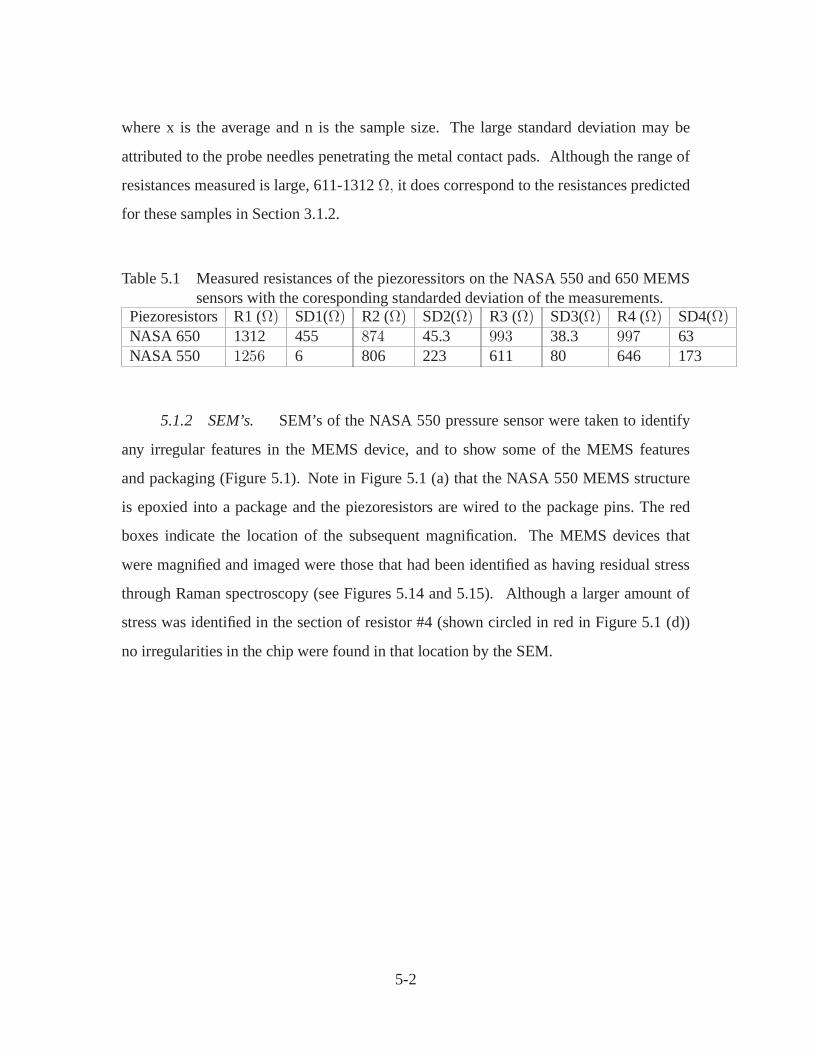
where x is the average and n is the sample size. The large standard deviation may be
attributed to the probe needles penetrating the metal contact pads. Although the range of
resistances measured is large, 611-1312 Ω, it does correspond to the resistances predicted
for these samples in Section 3.1.2.
Table 5.1 Measured resistances of the piezoressitors on the NASA 550 and 650 MEMSsensors with the coresponding standarded deviation of the measurements.
Piezoresistors R1 (Ω) SD1(Ω) R2 (Ω) SD2(Ω) R3 (Ω) SD3(Ω) R4 (Ω) SD4(Ω)NASA 650 1312 455 874 45.3 993 38.3 997 63NASA 550 1256 6 806 223 611 80 646 173
5.1.2 SEM’s. SEM’s of the NASA 550 pressure sensor were taken to identify
any irregular features in the MEMS device, and to show some of the MEMS features
and packaging (Figure 5.1). Note in Figure 5.1 (a) that the NASA 550 MEMS structure
is epoxied into a package and the piezoresistors are wired to the package pins. The red
boxes indicate the location of the subsequent magnification. The MEMS devices that
were magnified and imaged were those that had been identified as having residual stress
through Raman spectroscopy (see Figures 5.14 and 5.15). Although a larger amount of
stress was identified in the section of resistor #4 (shown circled in red in Figure 5.1 (d))
no irregularities in the chip were found in that location by the SEM.
5-2
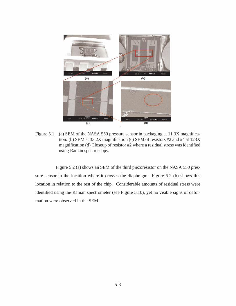
Figure 5.1 (a) SEM of the NASA 550 pressure sensor in packaging at 11.3X magnifica-tion. (b) SEM at 33.2X magnification (c) SEM of resistors #2 and #4 at 123Xmagnification (d) Closeup of resistor #2 where a residual stress was identifiedusing Raman spectroscopy.
Figure 5.2 (a) shows an SEM of the third piezoresistor on the NASA 550 pres-
sure sensor in the location where it crosses the diaphragm. Figure 5.2 (b) shows this
location in relation to the rest of the chip. Considerable amounts of residual stress were
identified using the Raman spectrometer (see Figure 5.10), yet no visible signs of defor-
mation were observed in the SEM.
5-3

(a) (b)(a) (b)(a) (b)(a) (b)
Figure 5.2 (a) SEM of resistor #3 on the NASA 550 pressure sensor in the location whereit crosses the diaphragm. (b) SEM of the NASA 550 pressure sensor showingthe location of (a)
5.1.3 Zygo Interferometer Data. An interferogram was made with a Zygo in-
terferometer to substantiate that a shift in the Raman spectrum of the resistive element
labeled #4 on the 550 NASA sample was caused by residual stress and not by an un-
even surface of that piezoresistor. The reason that the surface morphology is important
in Raman spectroscopy is that changes in the distance from the objective of the Raman
microscope to the object plane can cause a Raman shift if the laser is not refocused. The
Zygo, when operated properly, gives accurate measurements of the change in height of
the MEMS structures. In Figure 5.3, an interferometric measurement of resistors labeled
#2 and #4 (see Figure 3.1) were taken in an area identified as having residual stress by
Raman spectroscopy. It can be seen that there are only changes in their height where the
epilayer is grown, but that those structures are level on top and would not cause a Raman
shift. The two ellipses in green can be used as a reference to compare the interferogram
with the Raman map in Figure 5.15. Note that there are no visible defects in Figure 5.3
in the location of the residual stress shown in Figure 5.15, and that the area is completely
level from the interferogram.
5-4

Figure 5.3 An interferogram and a optical micrograph of the resistors #2 and #4 on theNASA 550 sample in a location where isolated residual stress was detectedusing Raman analysis.
Another interferometric measurement was recorded on resistor # 3 on the NASA
550 pressure sensor as shown in Figure 5.4. By Raman analysis, it was shown that as the
piezoresistor crosses the edge of the diaphragm, a considerable amount of residual stress
was detected (see Figure 5.10) that can effect the operation of the device. However,
through simple evaluation of the morphology of the structure, no variations could be de-
tected.
Figure 5.4 An interferogram and an optical micrograph of resistor # 3 on the NASA550 sample. Residual stress was identifed where the resistor crosses thediaphragm by using Raman spectroscopy.
5-5
5.1.4 Raman Spectroscopy on the NASA 550 MEMS. Several steps were taken
to determine the best way to collect the Raman spectral analysis data on sections of the
NASA 550 sample. The successful results are outlined in this section.
5.1.4.1 325-nm versus 514-nm Excitation. In order to determine which
frequency of light would be better to perform Raman spectral measurements on the crys-
talline 6H-SiC MEMS, both an Ar-ion laser with a wavelength of 514 nm and an ultra-
violet (UV) laser with a wavelength of 325 nm were used. For the 514 nm laser, a
1800/mm grating is designated and, for the 325-nm laser, a 2400/mm grating is desig-
nated. Even though the spectral resolution increases when a grating with a higher density
of lines is used, the system configuration still has better spectral resolution by using a
514-nm laser than the setup using the 325-nm laser. In Figure 5.5 (a), the spectrum of
crystalline 6H-SiC was recorded using the 514-nm excitation source. The TO1 peak at
766-cm−1, the TO2 peak at 788-cm−1and the LO peak at 966-cm−1are clearly discernible.
Each subplot in Figure 5.5 is zoomed in closer onto the TO peaks. In Figure 5.5 (b), the
Raman spectrum of crystalline 6H-SiC with a 325-nm laser excitation source is shown.
Notice that the spectral lines are less clearly resolved. The two reasons for this are that
the spectral resolution of the monochromator in the Raman system is lower for the 325-nm
excitation source than for the 514-nm source, and the 325-nm source can cause fluores-
cence because it exceeds the 3.0 eV band gap of 6H-SiC.
5-6
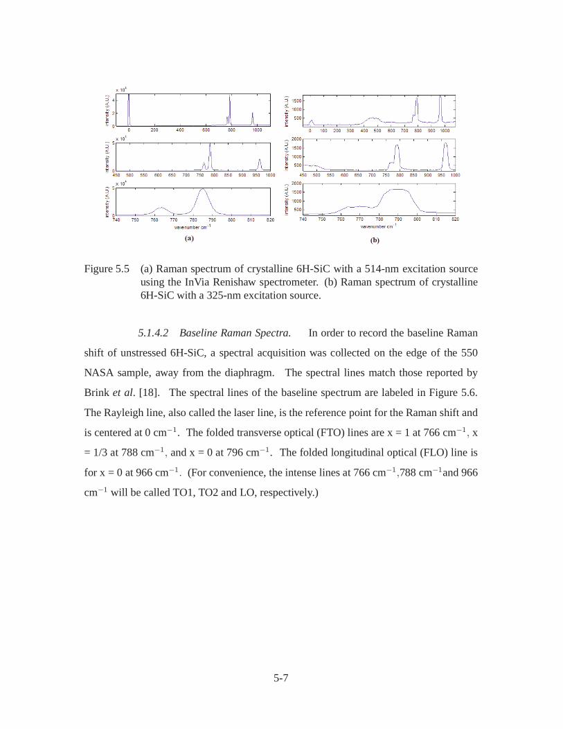
Figure 5.5 (a) Raman spectrum of crystalline 6H-SiC with a 514-nm excitation sourceusing the InVia Renishaw spectrometer. (b) Raman spectrum of crystalline6H-SiC with a 325-nm excitation source.
5.1.4.2 Baseline Raman Spectra. In order to record the baseline Raman
shift of unstressed 6H-SiC, a spectral acquisition was collected on the edge of the 550
NASA sample, away from the diaphragm. The spectral lines match those reported by
Brink et al. [18]. The spectral lines of the baseline spectrum are labeled in Figure 5.6.
The Rayleigh line, also called the laser line, is the reference point for the Raman shift and
is centered at 0 cm−1. The folded transverse optical (FTO) lines are x = 1 at 766 cm−1, x
= 1/3 at 788 cm−1, and x = 0 at 796 cm−1. The folded longitudinal optical (FLO) line is
for x = 0 at 966 cm−1. (For convenience, the intense lines at 766 cm−1,788 cm−1and 966
cm−1 will be called TO1, TO2 and LO, respectively.)
5-7
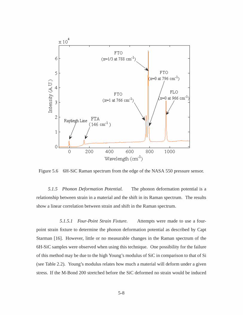
Figure 5.6 6H-SiC Raman spectrum from the edge of the NASA 550 pressure sensor.
5.1.5 Phonon Deformation Potential. The phonon deformation potential is a
relationship between strain in a material and the shift in its Raman spectrum. The results
show a linear correlation between strain and shift in the Raman spectrum.
5.1.5.1 Four-Point Strain Fixture. Attempts were made to use a four-
point strain fixture to determine the phonon deformation potential as described by Capt
Starman [16]. However, little or no measurable changes in the Raman spectrum of the
6H-SiC samples were observed when using this technique. One possibility for the failure
of this method may be due to the high Young’s modulus of SiC in comparison to that of Si
(see Table 2.2). Young’s modulus relates how much a material will deform under a given
stress. If the M-Bond 200 stretched before the SiC deformed no strain would be induced
5-8
on the crystal. In Starman and Lee et al. [1,16] experiments, they used thin films (1-2 µm)
which typically have a lower Young’s modulus than bulk samples [41]. In comparison, the
crystals that were tested in this experiment were 250-µm thick.
5.1.5.2 Vice. Measurement of the phonon deformation potential was also
attempted by the vice technique described in Chapter IV. The 6H-SiC sample was ex-
perimentally determined to have a shift in the TO1, TO2 and LO peaks as a function of
applied stress. As tensile stress was applied to the crystal, the peaks shifted to a lower
wavenumber in a linear fashion as seen in Figures 5.7 and 5.8; the data points were indi-
cated by blue circles. One important fact to note is that the resolution of the InVia Raman
spectrometer is larger then the smallest measurement tracked when measuring the Raman
shift in SiC as a function of stress. Because the Raman system is oversampled (refer to
Section 4.4.2) and each spectral peak is statistically fit with a Voigt profile using Wire
2.0R, the mean position of the peak is determined with resolution below the instrument
resolution. It is the mean positions that are plotted in Figures 5.7 and 5.8(top). The data
points were linearly fit using a least squares fit algorithm. The residuals chart (Figures
5.7 and 5.8 bottom) gives an indication of how closely the fit matched with the actual data
points. From the fit to the data shown in Figures 5.7 and 5.8, the TO1 and TO2 mode
frequencies are determined to be:
ωTO2(cm−1) = −3.02P + 788.4
ωTO1(cm−1) = −1.62P + 766.6 (5.3)
where P is a positive tensile pressure measured in GPa. The linearity of the TO2 mode
frequency is close to same as the results of Liu et al. [28]. The slight differences in the two
equations could be from different crystal faces, doping levels, crystal quality, experimental
setup or curve fitting techniques.
5-9

0 20 40 60 80 100 120 140 160-0.1
-0.05
0
0.05
0.1
0 50 100 150 200787.8
788
788.2
788.4
788.6
Pressure (MPa)
Wav
enum
ber
(cm-1
) y = - 0.0030216*x + 788.43
Wav
enum
ber
(cm-1
)
Pressure (MPa)
TO 2 linear
Figure 5.7 The top graph shows the line center of the TO2 peak as a function of uniaxialpressure applied normal to the c-axis of 6H-SiC. The bottom graph shows theresiduals of the linear least squares fit to the measured data points.
Figure 5.8 shows the line centers of the TO1 peak as a function of applied stress,
with a linear least squares fit and a plot of the corresponding residuals. By comparing the
slope of the TO1 line in Figure 5.8 with the slope of TO2 line in the Figure 5.7, it becomes
apparent that the TO2 line has a greater shift with respect to stress than the TO1 peak. The
fact that the TO1 peak shifts less than the TO2 peak was further confirmed in line scans
across the edge of the diaphragm of the NASA 550 pressure sensor, where the shift of the
line center of the two peaks was tracked separately (see Figure 5.10). From these results,
the TO2 peak is chosen to map areas of changes in the Raman shift due to residual stress.
5-10

0 20 40 60 80 100 120 140 160
-0.2
0
0.2residualsLinear: norm of residuals = 0.60969
Pressure (MPa)
Wav
enum
ber
(cm
-1)
0 20 40 60 80 100 120 140 160 180766.2
766.4
766.6
766.8
767
Pressure (MPa)
Wav
enum
ber
(cm
-1)
y = - 0.0016209*x + 766.57TO1 linear
Figure 5.8 The top graph shows the line center of the TO1 peak as a function of uniaxialpressure applied normal to the c-axis of 6H-SiC. The bottom graph shows theresiduals of the linear least squares fit to the measured data points.
5.1.5.3 Line Scans. Once the Raman spectra of 6H-SiC were determined
for unstressed and stressed crystals, measurements were performed by line scans to collect
the Raman spectra at each point on the sample in 5-µm steps using a computer controlled
piezoelectric stage. Figure 5.9 (a) shows the location of one line scan across resistor
#3. Figure 5.9 (b) shows where resistor #3 is located on the NASA 550 pressure sensor.
In Figure 5.9 it can be seen that the scan crosses the edge of the diaphragm which is
determined to be a location of residual stress from fabrication procedures.
5-11
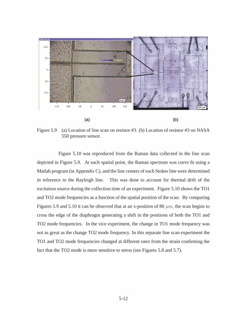
(a) (b)(a) (b)
Figure 5.9 (a) Location of line scan on resistor #3. (b) Location of resistor #3 on NASA550 pressure sensor.
Figure 5.10 was reproduced from the Raman data collected in the line scan
depicted in Figure 5.9. At each spatial point, the Raman spectrum was curve fit using a
Matlab program (in Appendix C), and the line centers of each Stokes line were determined
in reference to the Rayleigh line. This was done to account for thermal drift of the
excitation source during the collection time of an experiment. Figure 5.10 shows the TO1
and TO2 mode frequencies as a function of the spatial position of the scan. By comparing
Figures 5.9 and 5.10 it can be observed that at an x-position of 80 µm, the scan begins to
cross the edge of the diaphragm generating a shift in the positions of both the TO1 and
TO2 mode frequencies. In the vice experiment, the change in TO1 mode frequency was
not as great as the change TO2 mode frequency. In this separate line scan experiment the
TO1 and TO2 mode frequencies changed at different rates from the strain confirming the
fact that the TO2 mode is more sensitive to stress (see Figures 5.8 and 5.7).
5-12
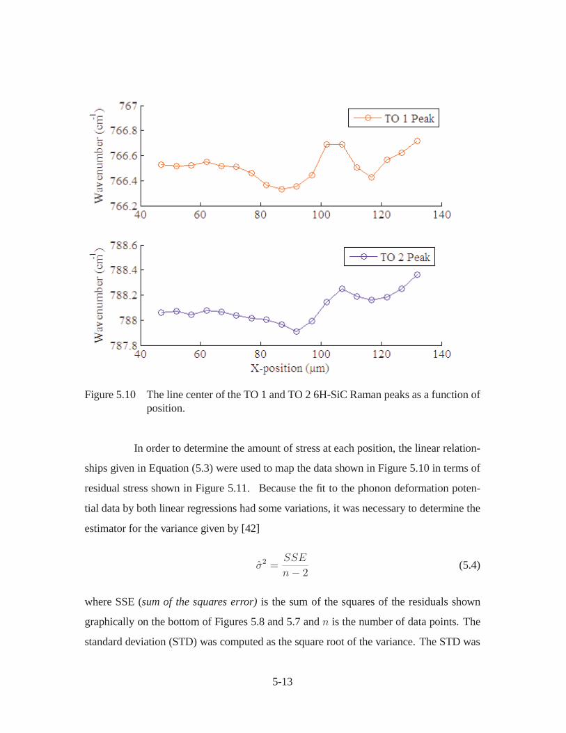
Figure 5.10 The line center of the TO 1 and TO 2 6H-SiC Raman peaks as a function ofposition.
In order to determine the amount of stress at each position, the linear relation-
ships given in Equation (5.3) were used to map the data shown in Figure 5.10 in terms of
residual stress shown in Figure 5.11. Because the fit to the phonon deformation poten-
tial data by both linear regressions had some variations, it was necessary to determine the
estimator for the variance given by [42]
σ2 =SSE
n− 2 (5.4)
where SSE (sum of the squares error) is the sum of the squares of the residuals shown
graphically on the bottom of Figures 5.8 and 5.7 and n is the number of data points. The
standard deviation (STD) was computed as the square root of the variance. The STD was
5-13
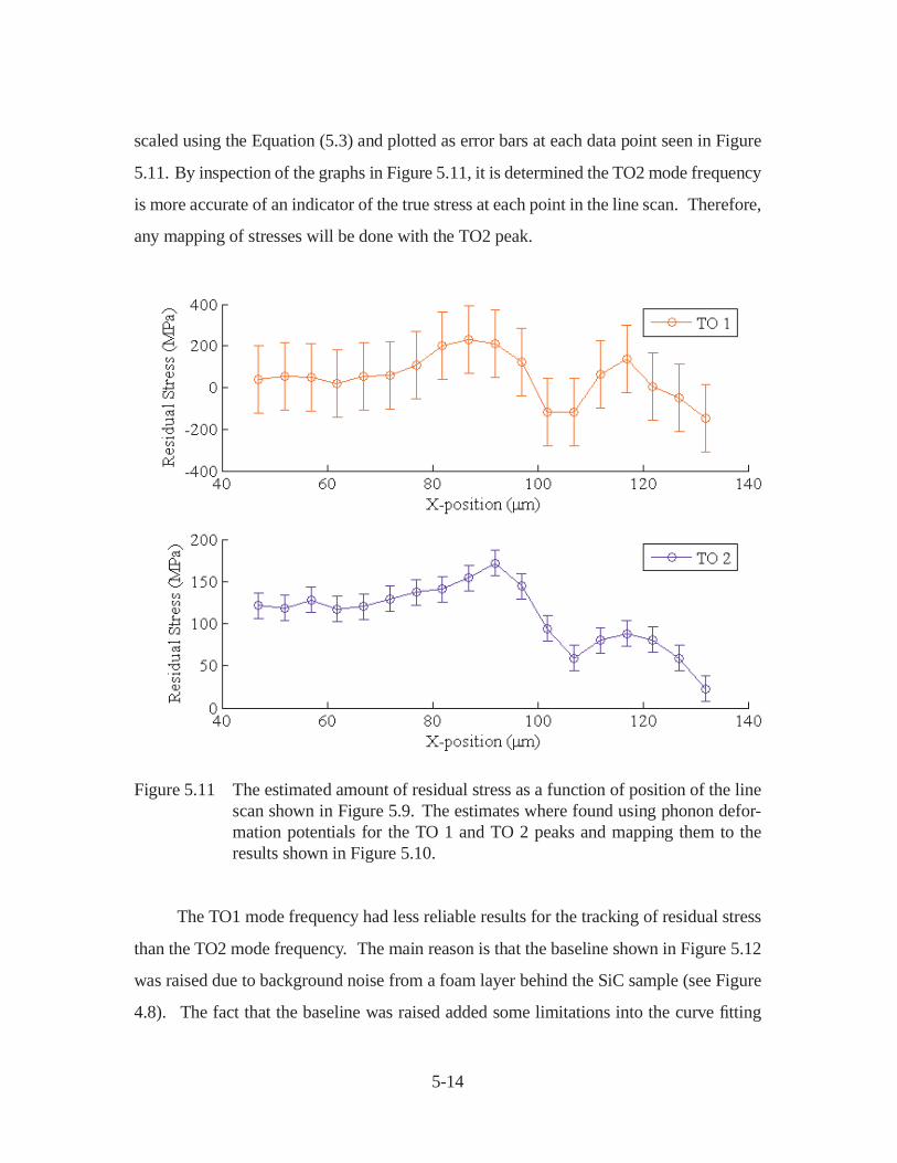
scaled using the Equation (5.3) and plotted as error bars at each data point seen in Figure
5.11. By inspection of the graphs in Figure 5.11, it is determined the TO2 mode frequency
is more accurate of an indicator of the true stress at each point in the line scan. Therefore,
any mapping of stresses will be done with the TO2 peak.
Figure 5.11 The estimated amount of residual stress as a function of position of the linescan shown in Figure 5.9. The estimates where found using phonon defor-mation potentials for the TO 1 and TO 2 peaks and mapping them to theresults shown in Figure 5.10.
The TO1 mode frequency had less reliable results for the tracking of residual stress
than the TO2 mode frequency. The main reason is that the baseline shown in Figure 5.12
was raised due to background noise from a foam layer behind the SiC sample (see Figure
4.8). The fact that the baseline was raised added some limitations into the curve fitting
5-14
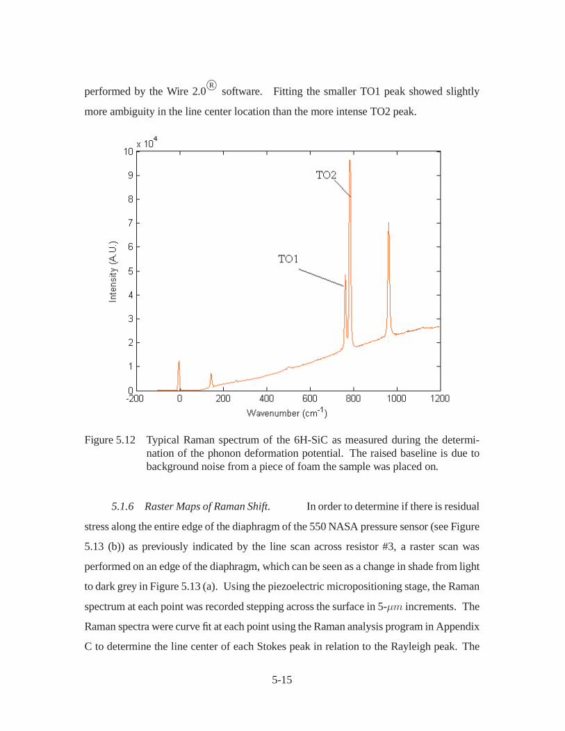
performed by the Wire 2.0R
software. Fitting the smaller TO1 peak showed slightly
more ambiguity in the line center location than the more intense TO2 peak.
Figure 5.12 Typical Raman spectrum of the 6H-SiC as measured during the determi-nation of the phonon deformation potential. The raised baseline is due tobackground noise from a piece of foam the sample was placed on.
5.1.6 Raster Maps of Raman Shift. In order to determine if there is residual
stress along the entire edge of the diaphragm of the 550 NASA pressure sensor (see Figure
5.13 (b)) as previously indicated by the line scan across resistor #3, a raster scan was
performed on an edge of the diaphragm, which can be seen as a change in shade from light
to dark grey in Figure 5.13 (a). Using the piezoelectric micropositioning stage, the Raman
spectrum at each point was recorded stepping across the surface in 5-µm increments. The
Raman spectra were curve fit at each point using the Raman analysis program in Appendix
C to determine the line center of each Stokes peak in relation to the Rayleigh peak. The
5-15

TO2 mode frequency was recorded at each spatial position and then converted to stress
units by Equation (5.3). A map of residual stress along the edge of the diaphragm was
then plotted as a function of spatial position as depicted in Figure 5.13 (c).
Figure 5.13 (a) Micrograph of diaphragm edge through a 20X objective with a coordi-nate system that matches the raster map location in (c). (b) Micrograph ofthe NASA 550 pressure sensor depicting the location of the edge of the di-aphragm. (c) The residual stress measured using of a raster scan across theedge of the diaphragm.
5.1.6.1 Raster Scans Across Piezoresistors. From the large variance in
resistance of the piezoresistors, the question arose whether residual stresses are playing a
part in those measurements. The residual stresses in resistors #2 and #4 were measured,
and are shown in Figures 5.14 and 5.15. The scan was performed on the sample (Figure
5-16
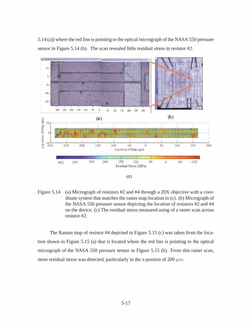
5.14 (a)) where the red line is pointing to the optical micrograph of the NASA 550 pressure
sensor in Figure 5.14 (b). The scan revealed little residual stress in resistor #2.
Figure 5.14 (a) Micrograph of resistors #2 and #4 through a 20X objective with a coor-dinate system that matches the raster map location in (c). (b) Micrograph ofthe NASA 550 pressure sensor depicting the location of resistors #2 and #4on the device. (c) The residual stress measured using of a raster scan acrossresistor #2.
The Raman map of resistor #4 depicted in Figure 5.15 (c) was taken from the loca-
tion shown in Figure 5.15 (a) that is located where the red line is pointing to the optical
micrograph of the NASA 550 pressure sensor in Figure 5.15 (b). From this raster scan,
more residual stress was detected, particularly in the x-postion of 200 µm.
5-17
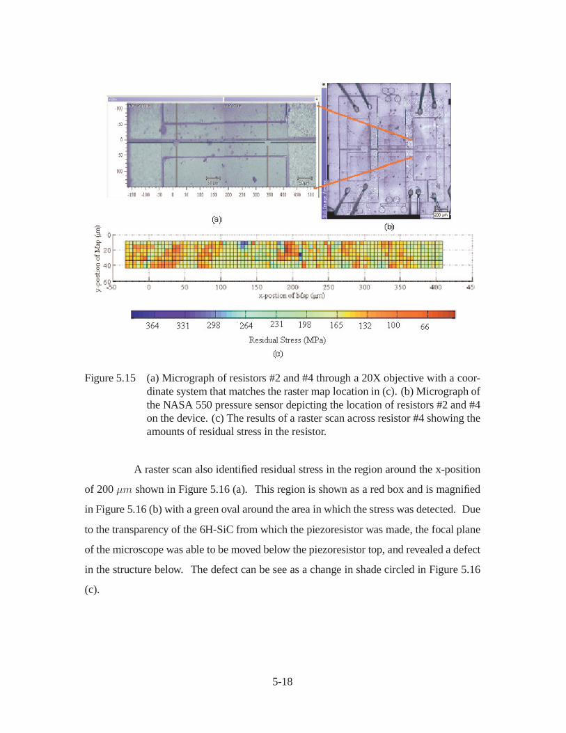
Figure 5.15 (a) Micrograph of resistors #2 and #4 through a 20X objective with a coor-dinate system that matches the raster map location in (c). (b) Micrograph ofthe NASA 550 pressure sensor depicting the location of resistors #2 and #4on the device. (c) The results of a raster scan across resistor #4 showing theamounts of residual stress in the resistor.
A raster scan also identified residual stress in the region around the x-position
of 200 µm shown in Figure 5.16 (a). This region is shown as a red box and is magnified
in Figure 5.16 (b) with a green oval around the area in which the stress was detected. Due
to the transparency of the 6H-SiC from which the piezoresistor was made, the focal plane
of the microscope was able to be moved below the piezoresistor top, and revealed a defect
in the structure below. The defect can be see as a change in shade circled in Figure 5.16
(c).
5-18
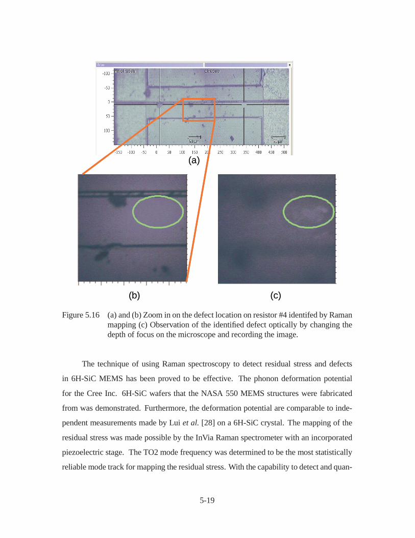
(a)
(b) (c)
(a)
(b) (c)
Figure 5.16 (a) and (b) Zoom in on the defect location on resistor #4 identifed by Ramanmapping (c) Observation of the identified defect optically by changing thedepth of focus on the microscope and recording the image.
The technique of using Raman spectroscopy to detect residual stress and defects
in 6H-SiC MEMS has been proved to be effective. The phonon deformation potential
for the Cree Inc. 6H-SiC wafers that the NASA 550 MEMS structures were fabricated
from was demonstrated. Furthermore, the deformation potential are comparable to inde-
pendent measurements made by Lui et al. [28] on a 6H-SiC crystal. The mapping of the
residual stress was made possible by the InVia Raman spectrometer with an incorporated
piezoelectric stage. The TO2 mode frequency was determined to be the most statistically
reliable mode track for mapping the residual stress. With the capability to detect and quan-
5-19
tify amounts of residual stress, the next step will be to determine a method of relieving the
stress from the fabrication processes.
5.2 Thin Film poly-SiC
Due to the nature of poly-SiC thin films (1.5 to 5 µm), the Raman spectra of the films
have proven to be more difficult to characterize than the Raman spectrum from the single-
crystal 6H-SiC MEMS devices provided by NASA. Attempts by Capt Stan Ness [39]
to identify residual stress in thin film poly-SiC by Raman spectroscopy using a 514-nm
excitation source on 1.5 to 2-µm films showed little success. In the experiments outlined in
this thesis, a 325-nm excitation source was used and 1.5–5-µm thick poly-SiC films were
investigated. The UV photons are well above the bandgap of SiC and are proven to be
highly absorptive (refer to in Figure A.1). This provides a resonant Raman effect, reduces
the amount of photons reaching the Si substrate, and therefore increases the signal-to-noise
ratio (SNR).
Several factors could influence the Raman spectra of the poly-SiC films including
possible stacking faults, grain boundaries, impurities and other polytypes found in the
poly-SiC. In addition, fluorescence of both the thin film of SiC and the Si substrate can
create background noise in the Raman spectrum and decrease the SNR.
5.2.1 325-nm versus 514-nm Excitation–Resonant Raman, Resolution and Lumi-
nescence. Raman spectroscopy of the same 1.5-µm poly-SiC thin films on (100) Si
substrate that Capt Ness [39] investigated with the 514-nm wavelength laser excitation
source was repeated. A cross-section of the sample is shown in Figure 3.4. The 514-nm
laser penetrates through the poly-SiC thin film with very little absorption or Raman ac-
tivity as shown in Figure 3.6, and much of the incident light is Raman scattered by the
Si substrate and shows up as the sharp peak at 521-cm−1 in Figure 5.17. Some of the
incident light is Raman scattered by the poly-SiC and shows up as broadened TO and LO
peaks.
5-20

For the same 1.5-µm poly-SiC thin films on (100) Si substrate, the 325-nm laser
excitation source produced much narrower TO and LO Raman peaks. The Raman spec-
trum recorded from the poly-SiC is shown in red in Figure 5.17. The characteristic modes
of 3C-SiC, TO at 791-cm−1 and the LO at 958-cm−1 were apparent. The Si mode was
also significantly diminished. The improved results using the UV excitation source are
attributed to two effects. One effect is the increased absorption of the poly-SiC film pre-
venting much of the incident laser light from reaching the substrate, and therefore reducing
the amount of Raman scattering from the substrate. The other effect is a resonant Raman
effect which increases the amplitude and sharpens TO and LO intensities as explained in
the Section 2.1 for this thesis and further detailed in Introduction to Raman Spectroscopy,
by Ferraro et al. [17].
0 200 400 600 800 1000 12000
1000
2000
3000
4000
5000
6000
7000
Wavenumber (cm-1
)
Inte
nsit
y (A
.U.)
325nm514nmSi
521 cm-1
3C-SiC TO791 cm-1
3C-SiC LO958 cm
-1
Laser Line
Figure 5.17 The blue spectral lines are from the Raman spectrum of a 1.5-µm poly-SiClayer on a (100) Si substrate measured using a 514-nm excitation source.The red spectral lines are of the same 1.5-µm poly-SiC film with a 325-nmexcitation source.
5.2.2 UV Raman Spectroscopy: Si versus SiC on Si. To further substantiate that
the peak around 500 cm−1 was due to the Si substrate, the Raman spectrum of (100) Si
5-21
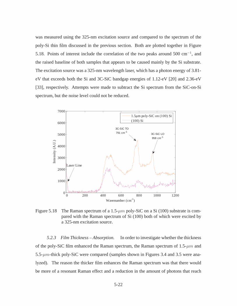
was measured using the 325-nm excitation source and compared to the spectrum of the
poly-Si thin film discussed in the previous section. Both are plotted together in Figure
5.18. Points of interest include the correlation of the two peaks around 500 cm−1, and
the raised baseline of both samples that appears to be caused mainly by the Si substrate.
The excitation source was a 325-nm wavelength laser, which has a photon energy of 3.81-
eV that exceeds both the Si and 3C-SiC bandgap energies of 1.12-eV [20] and 2.36-eV
[33], respectively. Attempts were made to subtract the Si spectrum from the SiC-on-Si
spectrum, but the noise level could not be reduced.
0 200 400 600 800 1000 12000
1000
2000
3000
4000
5000
6000
7000
Wavenumber (cm-1)
Inte
nsit
y (A
.U.)
1.5µm poly-SiC on (100) Si(100) Si
Laser Line
3C-SiC TO
791 cm-1 3C-SiC LO
958 cm-1
Figure 5.18 The Raman spectrum of a 1.5-µm poly-SiC on a Si (100) substrate is com-pared with the Raman spectrum of Si (100) both of which were excited bya 325-nm excitation source.
5.2.3 Film Thickness – Absorption. In order to investigate whether the thickness
of the poly-SiC film enhanced the Raman spectrum, the Raman spectrum of 1.5-µm and
5.5-µm-thick poly-SiC were compared (samples shown in Figures 3.4 and 3.5 were ana-
lyzed). The reason the thicker film enhances the Raman spectrum was that there would
be more of a resonant Raman effect and a reduction in the amount of photons that reach
5-22
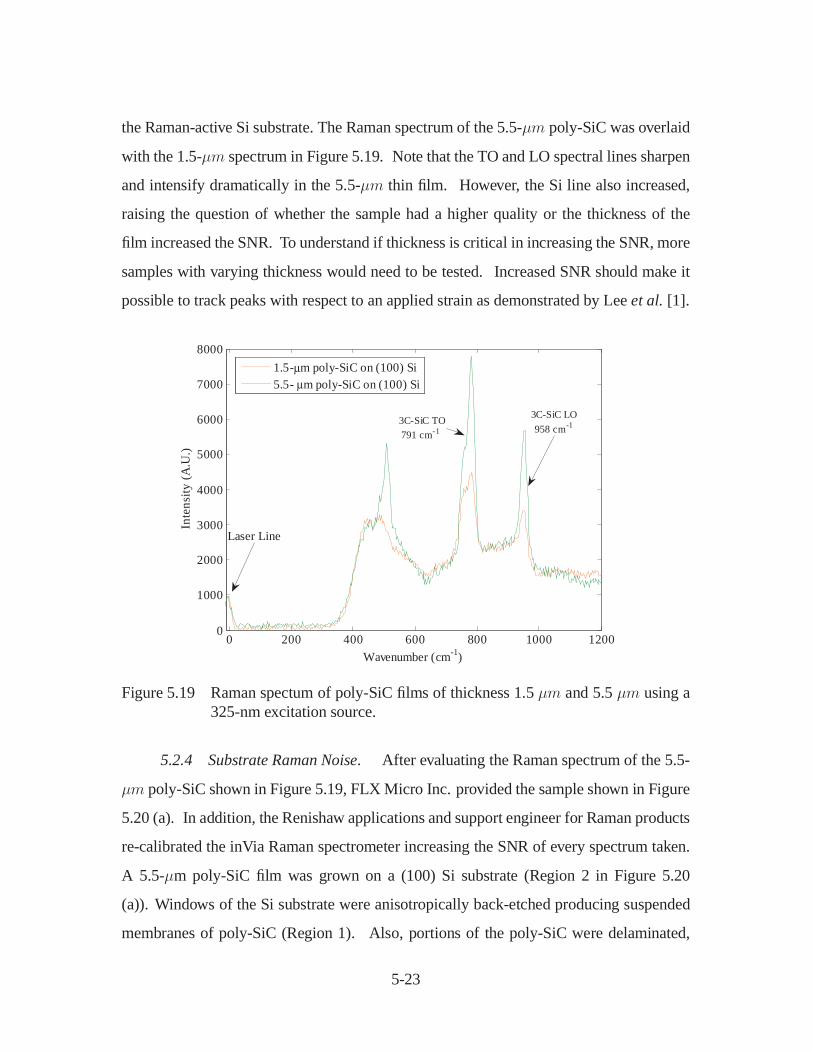
the Raman-active Si substrate. The Raman spectrum of the 5.5-µm poly-SiC was overlaid
with the 1.5-µm spectrum in Figure 5.19. Note that the TO and LO spectral lines sharpen
and intensify dramatically in the 5.5-µm thin film. However, the Si line also increased,
raising the question of whether the sample had a higher quality or the thickness of the
film increased the SNR. To understand if thickness is critical in increasing the SNR, more
samples with varying thickness would need to be tested. Increased SNR should make it
possible to track peaks with respect to an applied strain as demonstrated by Lee et al. [1].
0 200 400 600 800 1000 12000
1000
2000
3000
4000
5000
6000
7000
8000
Wavenumber (cm-1)
Inte
nsit
y (A
.U.)
1.5-µm poly-SiC on (100) Si5.5- µm poly-SiC on (100) Si
Laser Line
3C-SiC TO
791 cm-1
3C-SiC LO
958 cm-1
Figure 5.19 Raman spectum of poly-SiC films of thickness 1.5 µm and 5.5 µm using a325-nm excitation source.
5.2.4 Substrate Raman Noise. After evaluating the Raman spectrum of the 5.5-
µm poly-SiC shown in Figure 5.19, FLX Micro Inc. provided the sample shown in Figure
5.20 (a). In addition, the Renishaw applications and support engineer for Raman products
re-calibrated the inVia Raman spectrometer increasing the SNR of every spectrum taken.
A 5.5-µm poly-SiC film was grown on a (100) Si substrate (Region 2 in Figure 5.20
(a)). Windows of the Si substrate were anisotropically back-etched producing suspended
membranes of poly-SiC (Region 1). Also, portions of the poly-SiC were delaminated,
5-23
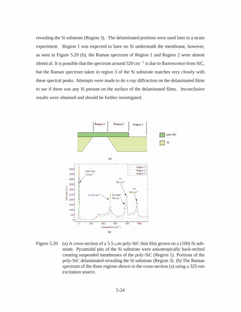
revealing the Si substrate (Region 3). The delaminated portions were used later in a strain
experiment. Region 1 was expected to have no Si underneath the membrane, however,
as seen in Figure 5.20 (b), the Raman spectrum of Region 1 and Region 2 were almost
identical. It is possible that the spectrum around 520 cm−1 is due to fluorescence from SiC,
but the Raman spectrum taken in region 3 of the Si substrate matches very closely with
these spectral peaks. Attempts were made to do x-ray diffraction on the delaminated films
to see if there was any Si present on the surface of the delaminated films. Inconclusive
results were obtained and should be further investigated.
Figure 5.20 (a) A cross-section of a 5.5-µm poly-SiC thin film grown on a (100) Si sub-strate. Pyramidal pits of the Si substrate were anisotropically back-etchedcreating suspended membranes of the poly-SiC (Region 1). Portions of thepoly-SiC delaminated revealing the Si substrate (Region 3). (b) The Ramanspectrum of the three regions shown in the cross-section (a) using a 325-nmexcitation source.
5-24
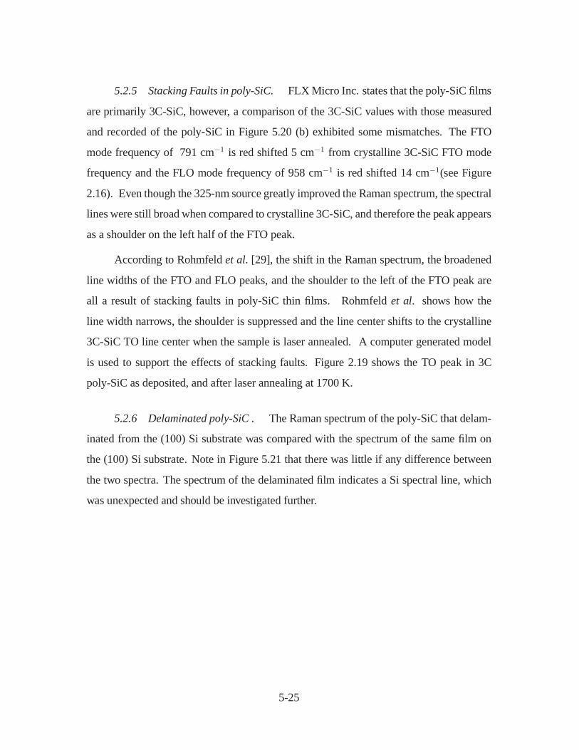
5.2.5 Stacking Faults in poly-SiC. FLX Micro Inc. states that the poly-SiC films
are primarily 3C-SiC, however, a comparison of the 3C-SiC values with those measured
and recorded of the poly-SiC in Figure 5.20 (b) exhibited some mismatches. The FTO
mode frequency of 791 cm−1 is red shifted 5 cm−1 from crystalline 3C-SiC FTO mode
frequency and the FLO mode frequency of 958 cm−1 is red shifted 14 cm−1(see Figure
2.16). Even though the 325-nm source greatly improved the Raman spectrum, the spectral
lines were still broad when compared to crystalline 3C-SiC, and therefore the peak appears
as a shoulder on the left half of the FTO peak.
According to Rohmfeld et al. [29], the shift in the Raman spectrum, the broadened
line widths of the FTO and FLO peaks, and the shoulder to the left of the FTO peak are
all a result of stacking faults in poly-SiC thin films. Rohmfeld et al. shows how the
line width narrows, the shoulder is suppressed and the line center shifts to the crystalline
3C-SiC TO line center when the sample is laser annealed. A computer generated model
is used to support the effects of stacking faults. Figure 2.19 shows the TO peak in 3C
poly-SiC as deposited, and after laser annealing at 1700 K.
5.2.6 Delaminated poly-SiC . The Raman spectrum of the poly-SiC that delam-
inated from the (100) Si substrate was compared with the spectrum of the same film on
the (100) Si substrate. Note in Figure 5.21 that there was little if any difference between
the two spectra. The spectrum of the delaminated film indicates a Si spectral line, which
was unexpected and should be investigated further.
5-25
Figure 5.21 The spectrum of 5.5-µm SiC on Si and SiC on Plexiglas.
The poly-SiC film was bonded, along with a strain gauge, to a piece of Plexiglas
glass using M-bond 200 adhesive. The assembly was then placed on the 4-point strain
fixture, and a uniform compressive stress was applied. The stress was measured by a
strain indicator and recorder. The TO, LO and laser line peaks were curve fit using Wire
2.0R
, and the center of the curves were tracked as a function of compressive stress. Unex-
pectedly, the peak centers did not shift as a function of stress (see Figure 5.22), indicating
that either no stress was felt by the film or the phonon modes are not sufficiently sensitive
to stress in this poly-SiC to monitor. More experiments should be made to identify the
phonon deformation potentials of the poly-SiC.
5-26
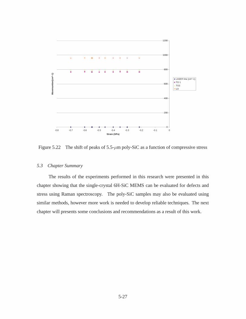
0
200
400
600
800
1000
1200
-0.8 -0.7 -0.6 -0.5 -0.4 -0.3 -0.2 -0.1 0
Strain (GPa)
Wa
ven
um
ber
(cm
^-1)
LASER line (cm^-1)
TO 1
TO2
LO
Figure 5.22 The shift of peaks of 5.5-µm poly-SiC as a function of compressive stress
5.3 Chapter Summary
The results of the experiments performed in this research were presented in this
chapter showing that the single-crystal 6H-SiC MEMS can be evaluated for defects and
stress using Raman spectroscopy. The poly-SiC samples may also be evaluated using
similar methods, however more work is needed to develop reliable techniques. The next
chapter will presents some conclusions and recommendations as a result of this work.
5-27
VI. Conclusions and Recommendations
The objective of this research, to determine a NDE method of identifying residual stress,
stress gradients and defects in SiC MEMS, was met. First the phonon deformation po-
tentials, that show a correlation between variations the Raman spectrum of SiC and stress
on the crystal structure, were determined. Then a NDE technique was developed that em-
ploys the spacial mapping of the Raman spectrum across SiC MEMS allowing for visual
identification of areas containing residual stress and defects.
6.1 Conclusions
The evolution of the stress states from raw materials to fabrication of SiC MEMS
is very important (i.e., process-induced changes in the microstucture). Baseline mea-
surements allow the understanding of the operation-based evolution of the microstructure
due to shock, high temperature, high voltage, ect. µ−Raman spectroscopy is becoming
important due to the repeated demonstrations of the ability to measure microstresses in
SiC materials. The experiments performed sought to address the underlying problem of
defects and microstress associated with SiC MEMS.
This research contributed to the state of the art in the detection and measurement
of residual stress in a variety of SiC-based MEMS structures. Raman spectroscopy pro-
vides the means to obtain microstructural information. The spectroscopic techniques
were adapted and applied to different crystal structures, both single crystalline and poly-
crystalline, and two different polytypes, 6H and 3C.
To the best of our knowledge, this work is the first study of residual stress corre-
sponding with defects in single crystal SiC MEMS devices. The work is also one of the
first studies on stress detection in polycrystalline SiC [20]. The results presented here are
important in the understanding of SiC materials. The measurement of deformation poten-
tial show linear results that correlate stress to Raman shift. Another important capability
of Raman spectroscopy is the mapping of residual stress states in MEMS devices. Defects
6-1
and stress networks within the samples were identified by Raman maps. Stacking-fault
observations in polycrystalline Raman spectra were evidenced by broadening of the Stokes
peaks.
The pioneering work in SiC represents a significant improvement in understanding
this development of residual stress in a variety of crystal structures. Raman spectroscopy
provides a non-destructive evaluation capability to optimize process output in device fab-
rication by identifying defects in raw material.
6.2 Recommendations for Future Work
In the work cmpleted for this thesis, Raman spectroscopy has been determined to be
a excellent method of locating residual stress and defects in SiC MEMS. The magnitude
of residual stress is further quantified by the determination of the phonon deformation po-
tential for 6H-SiC MEMS. To better quantify the relationship between stress and Raman
shift for 6H-SiC, a diamond anvil cell setup similar to Liu et al. [28] should be used to
compare the phonon deformation potential of 3.51 and 0.49 off axis 6H-SiC. With the
capability to detect and quantify amounts of residual stress in SiC MEMS, the next step
will be to determine a method of relieving the stress induced in the fabrication processes.
Some ideas on how to relieve the residual stress in the MEMS structures are with ion
implantation, high temperature annealing or by nuclear radiation [43].
Efforts in this research have also indicated that MEMS fabricated from thin-film
polycrystalline 3C-SiC on (100) Si substrates can be evaluated for residual stress using
UV resonate µ−Raman techniques. Investigation should include the recording of the
Raman spectrum of 10-µm thick poly-SiC film on (100) Si and comparing those results to
the Raman spectra of the 5.5-µm and 1.5-µm films to understand if thickness is crutical
in increasing the SNR. The next step in the research into thin film SiC should follow
the outline of Capt. Starman’s method of characterization of residual stress in thin-film
MEMS (see Section 2.3). The phonon deformation potential for 3C-SiC determined by
Lee et al. [1] should be verified. Some suggested methods are (1) an air pressure device
6-2
provided by FLX Micro Inc., (2) a 4-point bending fixture again (see [1]), (3) a vice to
induce stress as was used for the 6H-SiC or (4) the use of a diamond anvil cell. Once
this is complete, fix-fixed beams and cantilevers could be fabricated out of poly-SiC and
residual stress measured before and after release. Then, attempts to relieve stress could be
made using some of the techniques listed in the previous paragraph.
Another area of research interest is the identification of the cause of the strong Si
Raman mode detected in the delaminated thin films of poly-SiC (see Section 5.2.6). At-
tempts were made to do x-ray diffraction on the delaminated films to see if there was any
Si present on the surface of the film. Inconclusive results were obtained and should be
further investigated.
Another interesting area of research related to this work is the investigation of
MEMS made from other wide band gap semiconductor materials.
6-3

Appendix A. Properties of SiC
The Electron Hall Mobility shown in Figure A.1 is used in the calculation of the resistivity
of the piezoresistive elements #2 and #4 on the NASA 550 sample (see Section 3.1.2).
Figure A.1 Electron Hall mobility as a function of donor density [33]. Used to determineresistivity of 6H-SiC piezoresistors.
The absorption coefficients as a function of photon energy shown in Figures A.2
and A.3 were used in Section 3.3.3 to determine the percent of Transmission of light in
6H-SiC as a function of material thickness.
A-1
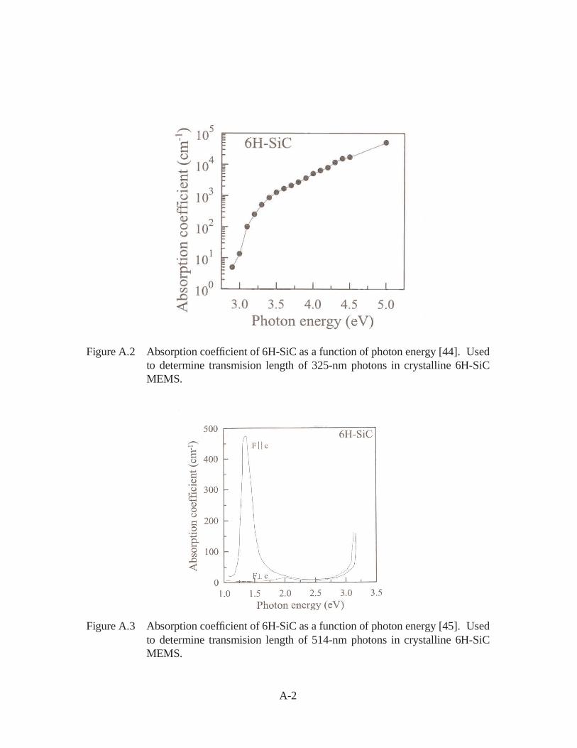
Figure A.2 Absorption coefficient of 6H-SiC as a function of photon energy [44]. Usedto determine transmision length of 325-nm photons in crystalline 6H-SiCMEMS.
Figure A.3 Absorption coefficient of 6H-SiC as a function of photon energy [45]. Usedto determine transmision length of 514-nm photons in crystalline 6H-SiCMEMS.
A-2
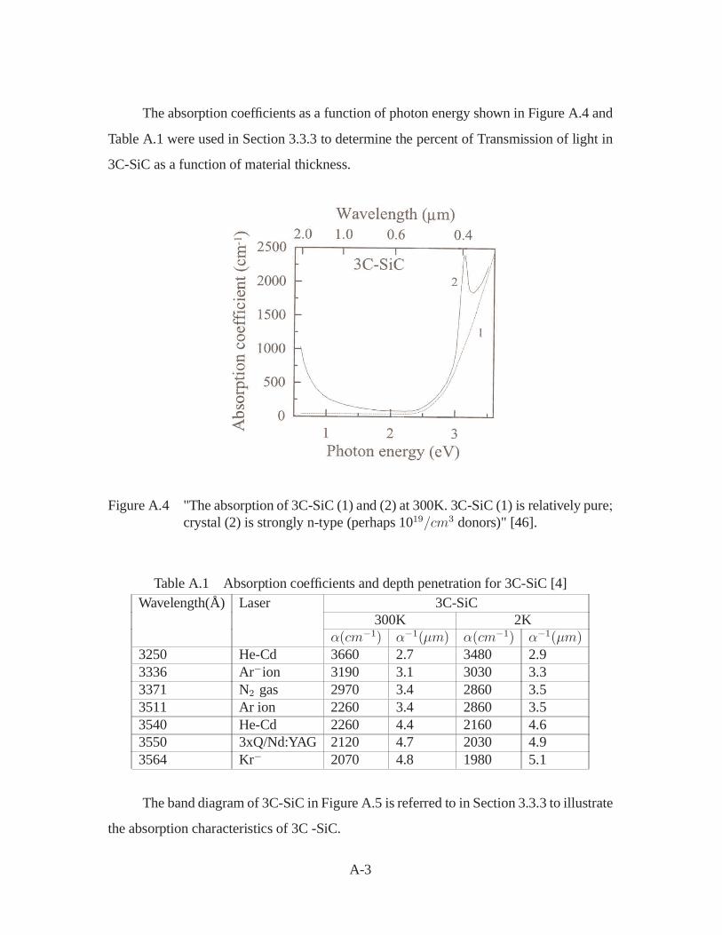
The absorption coefficients as a function of photon energy shown in Figure A.4 and
Table A.1 were used in Section 3.3.3 to determine the percent of Transmission of light in
3C-SiC as a function of material thickness.
Figure A.4 "The absorption of 3C-SiC (1) and (2) at 300K. 3C-SiC (1) is relatively pure;crystal (2) is strongly n-type (perhaps 1019/cm3 donors)" [46].
Table A.1 Absorption coefficients and depth penetration for 3C-SiC [4]Wavelength(Å) Laser 3C-SiC
300K 2Kα(cm−1) α−1(µm) α(cm−1) α−1(µm)
3250 He-Cd 3660 2.7 3480 2.93336 Ar−ion 3190 3.1 3030 3.33371 N2 gas 2970 3.4 2860 3.53511 Ar ion 2260 3.4 2860 3.53540 He-Cd 2260 4.4 2160 4.63550 3xQ/Nd:YAG 2120 4.7 2030 4.93564 Kr− 2070 4.8 1980 5.1
The band diagram of 3C-SiC in Figure A.5 is referred to in Section 3.3.3 to illustrate
the absorption characteristics of 3C -SiC.
A-3
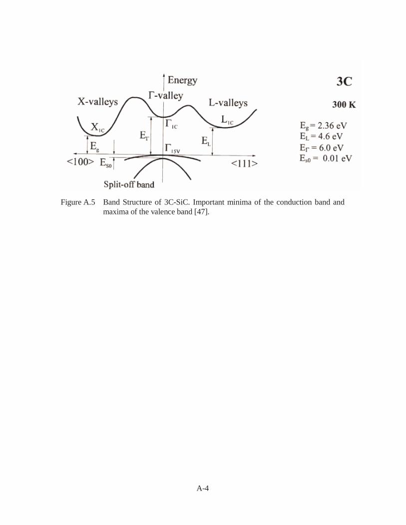
Figure A.5 Band Structure of 3C-SiC. Important minima of the conduction band andmaxima of the valence band [47].
A-4
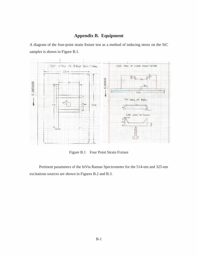
Appendix B. Equipment
A diagram of the four-point strain fixture test as a method of inducing stress on the SiC
samples is shown in Figure B.1.
Figure B.1 Four Point Strain Fixture
Pertinent parameters of the InVia Raman Spectrometer for the 514-nm and 325-nm
excitations sources are shown in Figures B.2 and B.3.
B-1
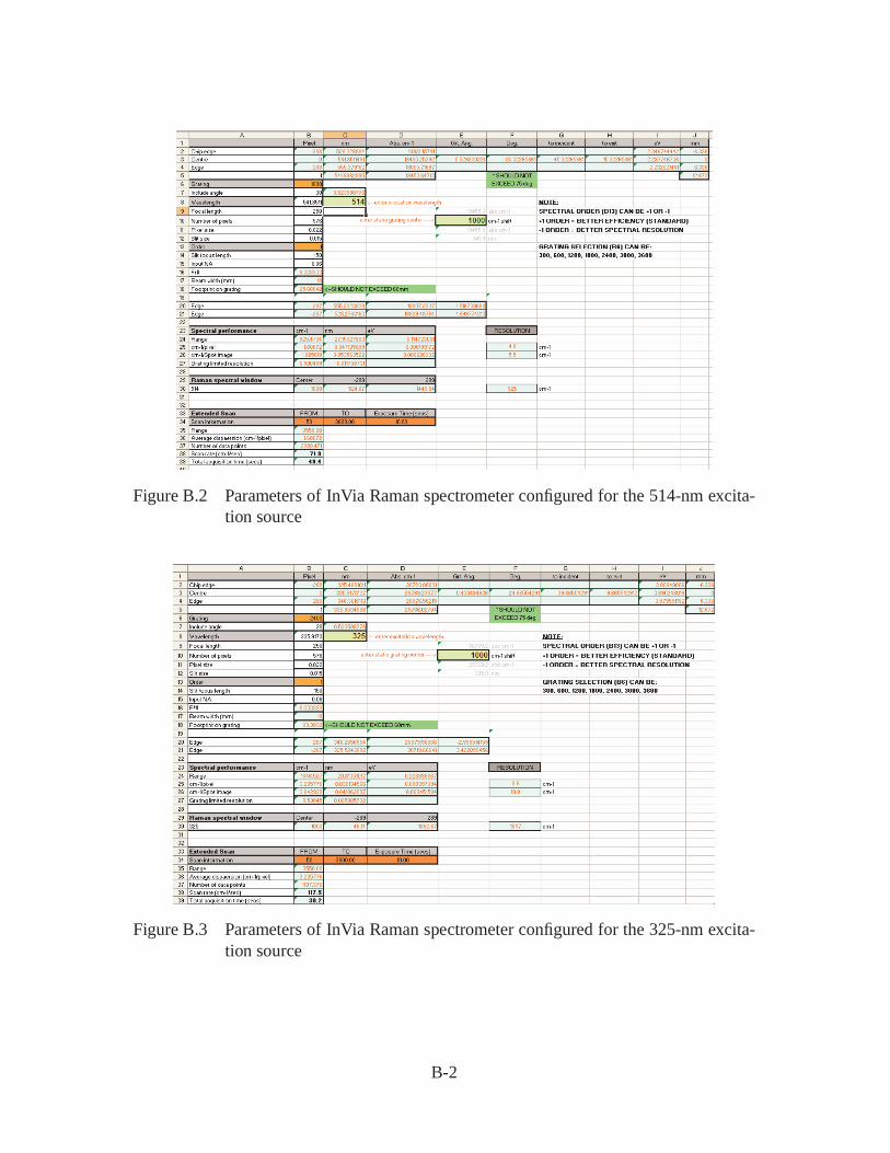
Figure B.2 Parameters of InVia Raman spectrometer configured for the 514-nm excita-tion source
Figure B.3 Parameters of InVia Raman spectrometer configured for the 325-nm excita-tion source
B-2
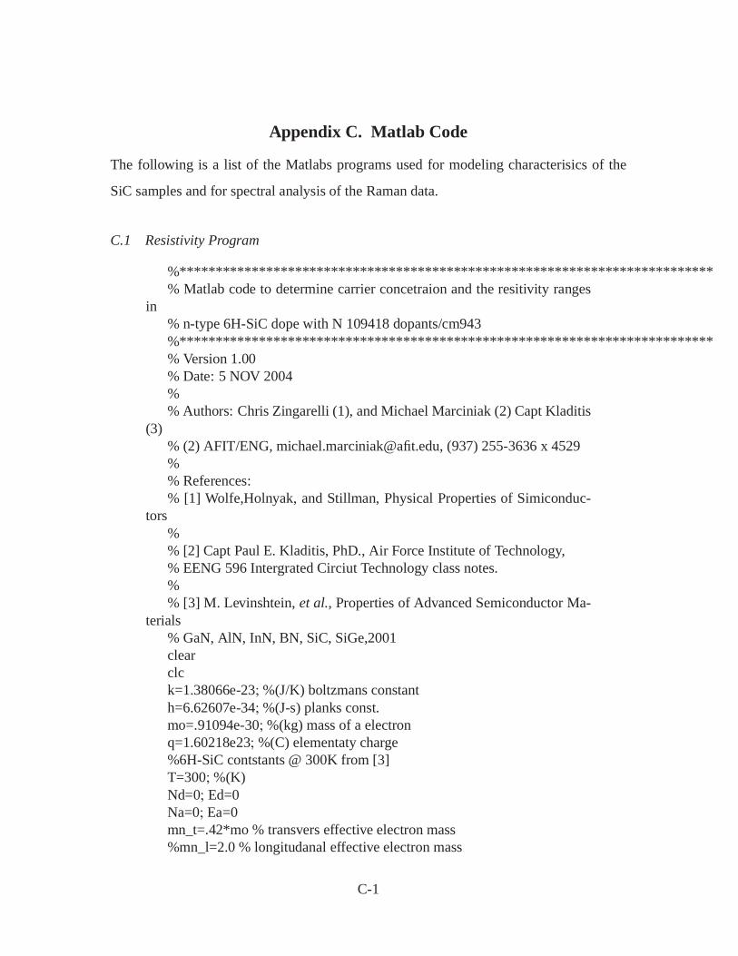
Appendix C. Matlab Code
The following is a list of the Matlabs programs used for modeling characterisics of the
SiC samples and for spectral analysis of the Raman data.
C.1 Resistivity Program
%**************************************************************************% Matlab code to determine carrier concetraion and the resitivity ranges
in% n-type 6H-SiC dope with N 109418 dopants/cm943%**************************************************************************% Version 1.00% Date: 5 NOV 2004%% Authors: Chris Zingarelli (1), and Michael Marciniak (2) Capt Kladitis
(3)% (2) AFIT/ENG, [email protected], (937) 255-3636 x 4529%% References:% [1] Wolfe,Holnyak, and Stillman, Physical Properties of Simiconduc-
tors%% [2] Capt Paul E. Kladitis, PhD., Air Force Institute of Technology,% EENG 596 Intergrated Circiut Technology class notes.%% [3] M. Levinshtein, et al., Properties of Advanced Semiconductor Ma-
terials% GaN, AlN, InN, BN, SiC, SiGe,2001clearclck=1.38066e-23;%(J/K) boltzmans constanth=6.62607e-34;%(J-s) planks const.mo=.91094e-30;%(kg) mass of a electronq=1.60218e23; %(C) elementaty charge%6H-SiC contstants @ 300K from [3]T=300;%(K)Nd=0; Ed=0Na=0; Ea=0mn_t=.42*mo % transvers effective electron mass%mn_l=2.0 % longitudanal effective electron mass
C-1
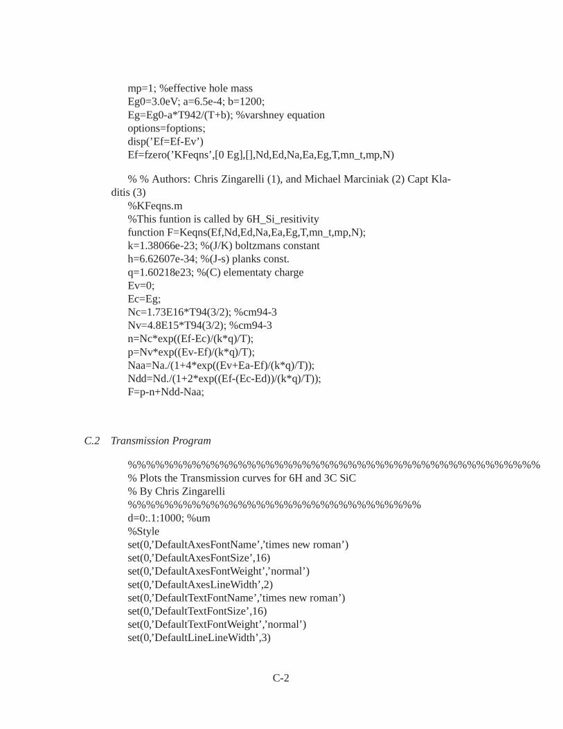
mp=1; %effective hole massEg0=3.0eV; a=6.5e-4; b=1200;Eg=Eg0-a*T942/(T+b);%varshney equationoptions=foptions;disp(’Ef=Ef-Ev’)Ef=fzero(’KFeqns’,[0 Eg],[],Nd,Ed,Na,Ea,Eg,T,mn_t,mp,N)
% % Authors: Chris Zingarelli (1), and Michael Marciniak (2) Capt Kla-ditis (3)
%KFeqns.m%This funtion is called by 6H_Si_resitivityfunction F=Keqns(Ef,Nd,Ed,Na,Ea,Eg,T,mn_t,mp,N);k=1.38066e-23;%(J/K) boltzmans constanth=6.62607e-34;%(J-s) planks const.q=1.60218e23; %(C) elementaty chargeEv=0;Ec=Eg;Nc=1.73E16*T94(3/2);%cm94-3Nv=4.8E15*T94(3/2);%cm94-3n=Nc*exp((Ef-Ec)/(k*q)/T);p=Nv*exp((Ev-Ef)/(k*q)/T);Naa=Na./(1+4*exp((Ev+Ea-Ef)/(k*q)/T));Ndd=Nd./(1+2*exp((Ef-(Ec-Ed))/(k*q)/T));F=p-n+Ndd-Naa;
C.2 Transmission Program
%%%%%%%%%%%%%%%%%%%%%%%%%%%%%%%%%%%%%%%%%%%%%% Plots the Transmission curves for 6H and 3C SiC% By Chris Zingarelli%%%%%%%%%%%%%%%%%%%%%%%%%%%%%%%%d=0:.1:1000;%um%Styleset(0,’DefaultAxesFontName’,’times new roman’)set(0,’DefaultAxesFontSize’,16)set(0,’DefaultAxesFontWeight’,’normal’)set(0,’DefaultAxesLineWidth’,2)set(0,’DefaultTextFontName’,’times new roman’)set(0,’DefaultTextFontSize’,16)set(0,’DefaultTextFontWeight’,’normal’)set(0,’DefaultLineLineWidth’,3)
C-2

% Absoption (um94-1)alpha_3C_325 = 3600e-4;alpha_3C_514 = 1.0e-2;alpha_6H_325 = 5000e-4;alpha_6H_514 = 2e-3;%transmissionT_3C_325=exp(-alpha_3C_325*d);T_3C_514=exp(-alpha_3C_514*d);T_6H_325=exp(-alpha_6H_325*d);T_6H_514=exp(-alpha_6H_514*d);semilogx(d,T_3C_325*100,’-’,d,T_3C_514*100,’-.’,d...,T_6H_325*100,’:’,d,T_6H_514*100,’–’);xlabel(’SiC film thickness (\mum)’);ylabel(’Percent of light transmited’);legend(’3C-SiC at 325nm’,’3C-SiC at 514nm’...,’6H-SiC at 325nm’,’6H-SiC at 514nm’);
C.3 Raman Analysis Program
%***************************************************% Micro-Raman Data Analysis Program (MRDAP)%*****************************************************% Version 2.10% Date: 04 January 2005% Changes: Add 3rd line in window, change tracking, add error analysis,% use own LSQ code.% S - folded (symmetry)% 0 Rayleigh% 126250 Fresnel lens line% 766.00 sto x = 1% 788.00 sto x = 1/3% 796.00 sto x = 0 (zone-centered)% 966.00 slo x = 0% Authors: Jason Foley(1), Chris Zingarelli (2), and Michael Marciniak
(2)% (1) AFRL/MNMF, [email protected], (850) 883-0584% (2) AFIT/ENG, [email protected], (937) 255-3636 x 4529%% References:% [1] Timucin, Dogan A., 2004, "A new computational framework for% atmospheric and surface remote sensing," Proc. ESTC 2004, B9P1,% pp. 1-7.
C-3

% [2] Puerta, Julio, and Martin, Pablo, 1981, "Three and four% generalized Lorentzian approximations for the Voigt% line shape," Appl. Opt., 20 (22), pp. 3923-3928.% [3] Foley, Jason R., et al., 2005, "Data reduction for micro-Raman% spectroscopy experiments," in preparation for submission to J.% Raman Spectroscopy.%function main()dbstop if errorclc;clear all;figure(1);clf;% Pseudocode% 1. Data Import% a. Baseline data file% b. Comparative data file(s)% 2. Plot% 3. Curve fitting% a. Gaussian + Lorentzian = Voigt!%————————————————————————-%% DATA IMPORT %%————————————————————————-%% File selection for data importation (GUI Codelet)% Set the default directorycd(’D:\Thesis\Zinger\Raman Spectrum’);for idf = 1:2 % Two passes: once for baseline, once for the rest of the data% Begin GUI codelet to select the data filesdirchange = true;while dirchange% Import data... dialog for file namecurrdir = cd;d = dir;str = d.name;isdir = [d.isdir];dirindices = find(isdir == true);dialogstr = str;for ii = 1:length(dirindices)dialogstr(ii) = [’<’,char(str(ii)),’>’];endif idf == 1;% SELECT BASELINE
C-4

[s,v] = listdlg(’PromptString’,’Select BASELINE data file:’,...’SelectionMode’,’single’,...’ListString’,dialogstr);else% SELECT DATA FILES (allow multiple files)[s,v] = listdlg(’PromptString’,’Select COMPARISON data file(s):’,...’SelectionMode’,’multiple’,...’ListString’,dialogstr);endif strcmp( ’..’,char(str(s)))% Chosen is directory... want to go up a levellastslash = max(findstr(currdir,’\’));currdir(lastslash+1:end) = [];cd(currdir);elseif strcmp( ’.’,char(str(s)))% Chosen is directory... want to refresh current directory... just% don’t allow anything to happen, as it will repopulate at% beginning of while loopelseif isdir(s)% Chosen is subdirectory... append to current path and start overcurrdir = [currdir,’\’,char(str(s))];cd(currdir);elsedirchange = false;endend% Read in data file(s)for iis = 1:length(s)filenameiis+idf-1 = d(s(iis)).name;if idf == 1;disp(sprintf(’Baseline file selected: %s.’,filenameiis+idf-1));elsedisp(sprintf(’Comparison file selected: %s.’,filenameiis+idf-1));end% Open the filefilecontents = importdata(filenameiis+idf-1);% try% head = file.textdata;% filedata = file.data;% colname = file.colheaders;% catchfiledata = filecontents;
C-5

% end[nrows,ncols] = size(filedata);switch ncolscase 2% Point scanscantypeiis+idf-1 = ’point’;Nscansiis+idf-1 = 1;dataiis+idf-1 = filedata(end:-1:1,1:2);case 4% X% Long vector of all positions...xveciis+idf-1 = filedata(end:-1:1,1);% Vector of unique positions (i.e., number of scans in the% x-direction)xscanposiis+idf-1 = unique(xveciis+idf-1);% Number of x’s that comprise each scanNxscanposiis+idf-1 = length(xscanposiis+idf-1);% Y% Long vector of all positions...yveciis+idf-1 = filedata(end:-1:1,2);% Vector of unique positions (i.e., number of scans in the% y-direction)yscanposiis+idf-1 = unique(yveciis+idf-1);% Number of y’s that comprise each scanNyscanposiis+idf-1 = length(yscanposiis+idf-1);if Nxscanposiis+idf-1 == 1% A vertical linescantypeiis+idf-1 = ’yline’;elseif Nyscanposiis+idf-1 == 1% A horizontal linescantypeiis+idf-1 = ’xline’;else% Area scan (raster, circle, or other)scantypeiis+idf-1 = ’area’;end% And in summary...Nscansiis+idf-1 = Nxscanposiis+idf-1*Nyscanposiis+idf-1;dataiis+idf-1 = filedata(end:-1:1,3:4);endendendNdatafiles = length(data);
C-6
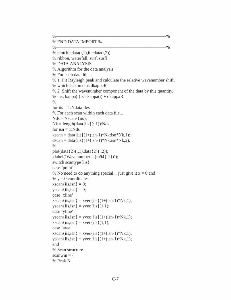
%————————————————————————-%% END DATA IMPORT %%————————————————————————-%% plot(filedata(:,1),filedata(:,2))% ribbon, waterfall, surf, surfl% DATA ANALYSIS% Algorithm for the data analysis% For each data file...% 1. Fit Rayleigh peak and calculate the relative wavenumber shift,% which is stored as dkappaR% 2. Shift the wavenumber component of the data by this quantity,% i.e., kappa(i) <- kappa(i) + dkappaR.%for iis = 1:Ndatafiles% For each scan within each data file...Nds = Nscansiis;Nk = length(dataiis(:,1))/Nds;for isn = 1:Ndskscan = dataiis(1+(isn-1)*Nk:isn*Nk,1);dscan = dataiis(1+(isn-1)*Nk:isn*Nk,2);%plot(data2(:,1),data2(:,2));xlabel(’Wavenumber k (m94-1)’);switch scantypeiiscase ’point’% No need to do anything special... just give it x = 0 and% y = 0 coordinates.xscaniis,isn = 0;yscaniis,isn = 0;case ’xline’xscaniis,isn = xveciis(1+(isn-1)*Nk,1);yscaniis,isn = yveciis(1,1);case ’yline’yscaniis,isn = yveciis(1+(isn-1)*Nk,1);xscaniis,isn = xveciis(1,1);case ’area’xscaniis,isn = xveciis(1+(isn-1)*Nk,1);yscaniis,isn = yveciis(1+(isn-1)*Nk,1);end% Scan structurescanwin = % Peak N
C-7

% kmin kmax Npeaks Name Center Sigma RelAmp-50 50 1 ’Rayleigh’ 0 1 1 ...” 0 1 0 ...” 0 1 0100 200 1 ’STA’ 150.5 3 1 ...” 0 1 0 ...” 0 1 0680 860 3 ’STO I,x=1’ 766.0 2 0.4 ...’STO II,x=1/3’ 788.0 2 1 ...’STO III,x=0’ 796.0 3 0.3900 1050 1 ’SLO’ 966.0 2 1 ...” 0 1 0 ...” 0 1 0;[Nwin,dum] = size(scanwin);for iw = 1:Nwin;% LINE WINDOWkmin = cell2mat(scanwin(iw,1));% cm94-1kmax = cell2mat(scanwin(iw,2)); % cm94-1a = min( find( kscan > kmin ) );% minimum indexb = max( find( kscan < kmax ) );% maximum indexNpeaks = cell2mat(scanwin(iw,3));% Number of peaks% PLOT DATA% Add to quick plotplot(kscan(a:b,1),dscan(a:b,1),’-r’);% LINE DATAk = kscan(a:b,1); % wavenumber datad = dscan(a:b,1); % intensity data% Estimate the noise in the sample from background data, i.e., the% 10 pts near the ends of the window for this peakidx = 10;bgydata = [d(1:idx,1);d(end-idx:end)];bgkdata = [k(1:idx,1);k(end-idx:end)];sigmad = std(bgydata);Rd = 1./sigmad;% Also, estimate the background from these pointsbgline = polyfit(bgkdata,bgydata,1);bgslope = bgline(1);bgoffset = bgline(2);% Estimate the peak values...pkpos = k(floor(mean(find(d == max(d))))); % finds middle of saturated
zone
C-8
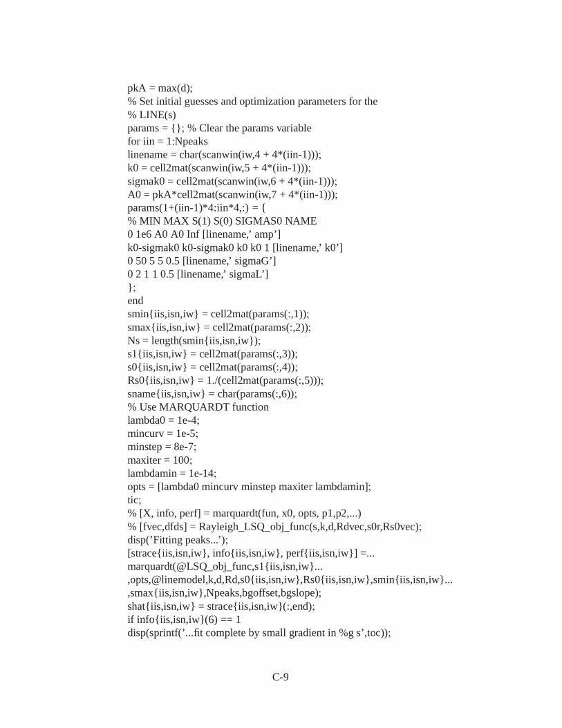
pkA = max(d);% Set initial guesses and optimization parameters for the% LINE(s)params = ; % Clear the params variablefor iin = 1:Npeakslinename = char(scanwin(iw,4 + 4*(iin-1)));k0 = cell2mat(scanwin(iw,5 + 4*(iin-1)));sigmak0 = cell2mat(scanwin(iw,6 + 4*(iin-1)));A0 = pkA*cell2mat(scanwin(iw,7 + 4*(iin-1)));params(1+(iin-1)*4:iin*4,:) = % MIN MAX S(1) S(0) SIGMAS0 NAME0 1e6 A0 A0 Inf [linename,’ amp’]k0-sigmak0 k0-sigmak0 k0 k0 1 [linename,’ k0’]0 50 5 5 0.5 [linename,’ sigmaG’]0 2 1 1 0.5 [linename,’ sigmaL’];endsminiis,isn,iw = cell2mat(params(:,1));smaxiis,isn,iw = cell2mat(params(:,2));Ns = length(sminiis,isn,iw);s1iis,isn,iw = cell2mat(params(:,3));s0iis,isn,iw = cell2mat(params(:,4));Rs0iis,isn,iw = 1./(cell2mat(params(:,5)));snameiis,isn,iw = char(params(:,6));% Use MARQUARDT functionlambda0 = 1e-4;mincurv = 1e-5;minstep = 8e-7;maxiter = 100;lambdamin = 1e-14;opts = [lambda0 mincurv minstep maxiter lambdamin];tic;% [X, info, perf] = marquardt(fun, x0, opts, p1,p2,...)% [fvec,dfds] = Rayleigh_LSQ_obj_func(s,k,d,Rdvec,s0r,Rs0vec);disp(’Fitting peaks...’);[straceiis,isn,iw, infoiis,isn,iw, perfiis,isn,iw] =...marquardt(@LSQ_obj_func,s1iis,isn,iw...,opts,@linemodel,k,d,Rd,s0iis,isn,iw,Rs0iis,isn,iw,sminiis,isn,iw...,smaxiis,isn,iw,Npeaks,bgoffset,bgslope);shatiis,isn,iw = straceiis,isn,iw(:,end);if infoiis,isn,iw(6) == 1disp(sprintf(’...fit complete by small gradient in %g s’,toc));
C-9

elseif infoiis,isn,iw(6) == 2disp(sprintf(’...fit complete by small step in %g s’,toc));elseif infoiis,isn,iw(6) == 3disp(sprintf(’...fit complete by max iterations in %g s’,toc));end[fhatiis,isn,iw,Jhatiis,isn,iw] = LSQ_obj_func(shatiis,isn,iw,...@linemodel,k,d,Rd,s0iis,isn,iw,Rs0iis,isn,iw,...sminiis,isn,iw,smaxiis,isn,iw,Npeaks,bgoffset,bgslope);% Perform error analysislastwarn(”);% clear all warnings% Mean square error for a MAP estimator is...MSEiis,isn,iw = inv( Jhatiis,isn,iw(1:end-Ns,:).’*Jhatiis,isn,iw(1:end-
Ns,:) + ...diag(Rs0iis,isn,iw).’*diag(Rs0iis,isn,iw) );if 126strcmp(lastwarn,”);trydisp(sprintf(’MSE is not well-conditioned: %g’,cond(MSE)));catchtryMSEiis,isn,iw = pinv( Jhatiis,isn,iw(1:end-Ns,:).’*Jhatriis,isn,iw(1:end-
Ns,:) + ...diag(Rs0iis,isn,iw).’*diag(Rs0iis,isn,iw) );catchMSEiis,isn,iw = zeros(Ns,Ns);endendendscaled_covarianceiis,isn,iw = MSEiis,isn,iw;sigmashatiis,isn,iw = diag(sqrt(MSEiis,isn,iw));sigmashatiis,isn,iw(find(sigmashatiis,isn,iw==0),1) = eps;for is = 1:Ns;scaled_covarianceiis,isn,iw(is,:) = ...scaled_covarianceiis,isn,iw(is,:)/sigmashatiis,isn,iw(is);scaled_covarianceiis,isn,iw(:,is) = ...scaled_covarianceiis,isn,iw(:,is)/sigmashatiis,isn,iw(is);end% Report estimation resultsfor is = 1:Nsdisp(sprintf(’%s = %g +/- %g; s(1) = %g.’,deblank(snameiis,isn,iw(is,:)),...shatiis,isn,iw(is),sigmashatiis,isn,iw(is),s1iis,isn,iw(is)));endif iw == 1;
C-10

% 2. Shift the wavenumber component of the data by this quantity,% i.e., kappa(i) <- kappa(i) + dkappaR.dkappaRiis,isn,iw = shatiis,isn,iw(2,1);kscan = kscan - dkappaRiis,isn,iw;% reloads each scan, so this is safeendendendend%% SAVE RESULTSfor iis = 2:Ndatafiles% SAVE TO DATA FILENds = Nscansiis;% Find the starting index of the file extensionstrstart = findstr(filenameiis,’.’);% Replace the file extension with a *.DAT file extensiondatfilename = [filenameiis(1:strstart),’dat’];% Write the header, which contains:% Line 1) the baseline data filenamefid = fopen(datfilename,’w’);HeaderString = [’Baseline data file: ’,filename1];fprintf(fid,’%s\n’,HeaderString);fprintf(fid,’\n’);% Line 2) the column headersDataColumnHeaders1 = ’x’;DataColumnHeaders2 = ’y’;count = 3;for iw = 1:Nwin;Ns = length(smin1,1,iw);for is = 1:NsDataColumnHeaderscount = deblank(sname1,1,iw(is,:));count = count + 1;endend%for ilf = 1:(length(DataColumnHeaders)-1)fprintf(fid,’%s, ’,DataColumnHeadersilf);endfprintf(fid,’%s’,DataColumnHeadersilf+1);% don’t need a commafprintf(fid,’\n’);for isn = 1:NdsDataColumnValues(1) = xscaniis,isn;
C-11
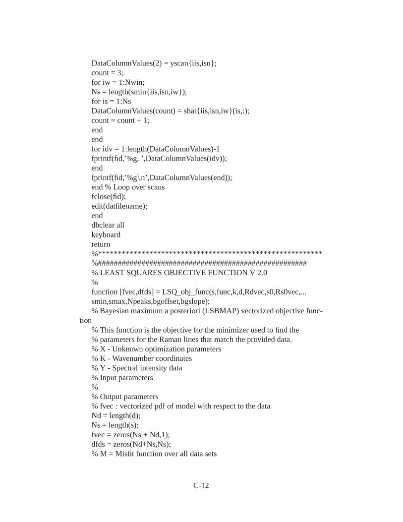
DataColumnValues(2) = yscaniis,isn;count = 3;for iw = 1:Nwin;Ns = length(sminiis,isn,iw);for is = 1:NsDataColumnValues(count) = shatiis,isn,iw(is,:);count = count + 1;endendfor idv = 1:length(DataColumnValues)-1fprintf(fid,’%g, ’,DataColumnValues(idv));endfprintf(fid,’%g\n’,DataColumnValues(end));end % Loop over scansfclose(fid);edit(datfilename);enddbclear allkeyboardreturn%*********************************************************%#####################################################% LEAST SQUARES OBJECTIVE FUNCTION V 2.0%function [fvec,dfds] = LSQ_obj_func(s,func,k,d,Rdvec,s0,Rs0vec,...smin,smax,Npeaks,bgoffset,bgslope);% Bayesian maximum a posteriori (LSBMAP) vectorized objective func-
tion% This function is the objective for the minimizer used to find the% parameters for the Raman lines that match the provided data.% X - Unknown optimization parameters% K - Wavenumber coordinates% Y - Spectral intensity data% Input parameters%% Output parameters% fvec : vectorized pdf of model with respect to the dataNd = length(d);Ns = length(s);fvec = zeros(Ns + Nd,1);dfds = zeros(Nd+Ns,Ns);% M = Misfit function over all data sets
C-12
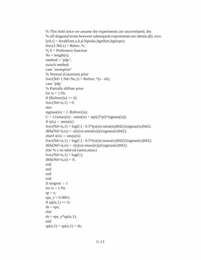
% This hold since we assume the experiments are uncorrelated; the% off-diagonal terms between subsequent experiments are identically zero.[y0,r] = feval(func,s,k,d,Npeaks,bgoffset,bgslope);fvec(1:Nd,1) = Rdvec.*r;% S = Preference functionNs = length(s);method = ’pdp’;switch methodcase ’normprior’% Normal (Gaussian) priorfvec(Nd+1:Nd+Ns,1) = Rs0vec.*(s - s0);case ’pdp’% Partially diffuse priorfor is = 1:Nsif (Rs0vec(is) == 0)fvec(Nd+is,1) = 0;elsesigmas(is) = 1./Rs0vec(is);C = 1/(smax(is) - smin(is) + sqrt(2*pi)*sigmas(is));if s(is) < smin(is)fvec(Nd+is,1) = log(C) - 0.5*((s(is)-smin(is))942)/(sigmas(is)942);dfds(Nd+is,is) = -((s(is)-smin(is)))/(sigmas(is)942);elseif s(is) > smax(is)fvec(Nd+is,1) = log(C) - 0.5*((s(is)-smax(is))942)/(sigmas(is)942);dfds(Nd+is,is) = -((s(is)-smax(is)))/(sigmas(is)942);else % s on interval (smin,smax)fvec(Nd+is,1) = log(C);dfds(Nd+is,is) = 0;endendendendif nargout > 1for is = 1:Nssp = s;eps_s = 0.0001;if sp(is,1) == 0;ds = eps;elseds = eps_s*sp(is,1);endsp(is,1) = sp(is,1) + ds;
C-13
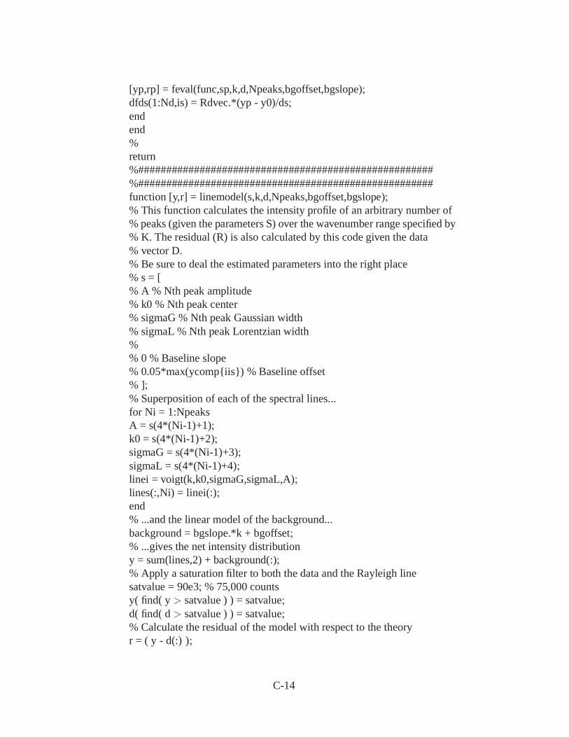
[yp,rp] = feval(func,sp,k,d,Npeaks,bgoffset,bgslope);dfds(1:Nd,is) = Rdvec.*(yp - y0)/ds;endend%return%#####################################################%#####################################################function [y,r] = linemodel(s,k,d,Npeaks,bgoffset,bgslope);% This function calculates the intensity profile of an arbitrary number of% peaks (given the parameters S) over the wavenumber range specified by% K. The residual (R) is also calculated by this code given the data% vector D.% Be sure to deal the estimated parameters into the right place% s = [% A % Nth peak amplitude% k0 % Nth peak center% sigmaG % Nth peak Gaussian width% sigmaL % Nth peak Lorentzian width%% 0 % Baseline slope% 0.05*max(ycompiis) % Baseline offset% ];% Superposition of each of the spectral lines...for Ni = 1:NpeaksA = s(4*(Ni-1)+1);k0 = s(4*(Ni-1)+2);sigmaG = s(4*(Ni-1)+3);sigmaL = s(4*(Ni-1)+4);linei = voigt(k,k0,sigmaG,sigmaL,A);lines(:,Ni) = linei(:);end% ...and the linear model of the background...background = bgslope.*k + bgoffset;% ...gives the net intensity distributiony = sum(lines,2) + background(:);% Apply a saturation filter to both the data and the Rayleigh linesatvalue = 90e3; % 75,000 countsy( find( y > satvalue ) ) = satvalue;d( find( d > satvalue ) ) = satvalue;% Calculate the residual of the model with respect to the theoryr = ( y - d(:) );
C-14
% Plot the resultsplot(k,d,’ok’,k,y,’-r’);xlabel(’Wavenumber (cm94-1)’);ylabel(’Intensity (A.U.)’);pause(0.001);return%########################################################%&&&&&&&&&&&&&&&&&&&&&&&&&&&&&&&&&&&&&&% VOIGT FUNCTION AND INTEGRAL%————————————————————————–function f = voigt(omega,omega0,sigmaG,sigmaL,A);% This is the "outer" subroutine for the Voigt profile...for iw = 1:length(omega)method = ’approximation’;switch methodcase ’approximation’% This is the approximation of the Voigt integral from Puerta and Martin,% 1981, ’Three and four generalized Lorentzian approximations for the
Voigt% line shape,’ Appl. Opt., 20 (22), pp. 3923-3928.p = abs(sigmaL/sigmaG); % must be positive to be in upper half-plane.d = ((omega(iw)-omega0)/sigmaG);z = p + i*d;f(iw) = 2*A*real(cef(i*z,10))/sqrt(pi);% f(iw) = A*real(erfw(z))/sqrt(pi);case ’integral’omegamax = 2.5*sigmaG;f(iw) = A*quadl(@voigtint,-omegamax,omegamax,[],[],...omega(iw),omega0,sigmaG,sigmaL);endendreturn%————————————————————————–% This is the integrand for the Voigt integral if usedfunction I = voigtint(omegastar,omega,omega0,sigmaG,sigmaL);% I = exp( - ((omegastar - omega0).942)./(sigmaG.942) ) ./...( (omegastar - omega - omega0).942 + sigmaL.942 );I = exp( - ((omegastar).942)./(sigmaG.942) ) ./ ...( ( (omega-omega0) - omegastar ).942 + sigmaL.942 );return%&&&&&&&&&&&&&&&&&&&&&&&&&&&&&&&&%
C-15
% CEF %% COMPLEX ERROR FUNCTION %%——————————————————————-%function w = cef(z,N)% Computes the function w(z) = exp(-z942) erfc(-iz) using a rational% series with N terms. It is assumed that Im(z) > 0 or Im(z) = 0.%% Andre Weideman, 1995M = 2*N;M2 = 2*M; k = [-M+1:1:M-1]’;% M2 = no. of sampling points.L = sqrt(N/sqrt(2));% Optimal choice of L.theta = k*pi/M; t = L*tan(theta/2); % Define variables theta and t.f = exp(-t.942).*(L942+t.942); f = [0; f];% Function to be transformed.a = real(fft(fftshift(f)))/M2;% Coefficients of transform.a = flipud(a(2:N+1));% Reorder coefficients.Z = (L+i*z)./(L-i*z); p = polyval(a,Z);% Polynomial evaluation.w = 2*p./(L-i*z).942+(1/sqrt(pi))./(L-i*z);% Evaluate w(z).%——————————————————————-%return % End CEF %%%&&&&&&&&&&&&&&&&&&&&&&&&&&&&&&&&function [X, info, perf] = marquardt(fun, x0, opts, varargin)%MARQUARDT Levenberg-Marquardt’s method for least squares.% Find xm = argminF(x) , where x is an n-vector and% F(x) = .5 * sum(f_i(x)942) .% The functions f_i(x) (i=1,...,m) and the Jacobian matrix J(x)% (with elements J(i,j) = Df_i/Dx_j ) must be given by a MATLAB% function with declaration% function [f, J] = fun(x,p1,p2,...)% p1,p2,... are parameters of the function. In connection with% nonlinear data fitting they may be arrays with coordinates of% the data points.%% Call% [X, info] = marquardt(fun, x0)% [X, info] = marquardt(fun, x0, opts, p1,p2,...)% [X, info, perf] = marquardt(.....)%% Input parameters% fun : Handle to the function.% x0 : Starting guess for xm .% opts : Vector with five elements.% opts(1) used in starting value for Marquardt parameter:
C-16
% mu = opts(1) * max(A0(i,i)) with A0 = J(x0)’*J(x0)% opts(2:4) used in stopping criteria:% ||F’||inf <= opts(2) or% ||dx||2 <= opts(3)*(opts(3) + ||x||2) or% no. of iteration steps exceeds opts(4) .% opts(5) lower bound on mu:% mu = opts(5) * max(A(i,i)) with A = J(x)’*J(x)% Default opts = [1e-3 1e-4 1e-8 100 1e-14]% If the input opts has less than 5 elements, it is% augmented by the default values.% p1,p2,.. are passed directly to the function FUN .%% Output parameters% X : If perf is present, then array, holding the iterates% columnwise. Otherwise, computed solution vector.% info : Performance information, vector with 6 elements:% info(1:4) = final values of% [F(x) ||F’||inf ||dx||2 mu/max(A(i,i))] ,% where A = J(x)’*J(x) .% info(5) = no. of iteration steps% info(6) = 1 : Stopped by small gradient% 2 : Stopped by small x-step% 3 : No. of iteration steps exceeded% -1 : x is not a real valued vector% -2 : f is not a real valued column vector% -3 : J is not a real valued matrix% -4 : Dimension mismatch in x, f, J% -5 : Overflow during computation% perf : Array, holding% perf(1,:) = values of F(x)% perf(2,:) = values of || F’(x) ||inf% perf(3,:) = mu-values.%% Method% Gauss-Newton with Levenberg-Marquardt damping, see eg% H.B. Nielsen, "Damping parameter in Marquardt’s method",% IMM-REP-1999-05, IMM, DTU, April 1999.% Version 04.05.18. hbn(a)imm.dtu.dk% Check parameters and function callif nargin < 3, opts = []; endopts = checkopts(opts, [1e-3 1e-4 1e-8 100 1e-14]);if nargin < 2, stop = -1;
C-17

else[stop x n] = checkx(x0);if 126stop, [stop F f J] = checkfJ(fun,x0,varargin:); endendif 126stopg = J’*f; ng = norm(g,inf); A = J’*J;if isinf(ng) | isinf(norm(A(:),inf)), stop = -5; endelseF = NaN; ng = NaN;endif stopX = x0; perf = []; info = [F ng 0 opts(1) 0 stop];returnend% Finish initializationmu = opts(1) * max(diag(A)); kmax = opts(4);Trace = nargout > 2;if TraceX = repmat(x,1,kmax+1);perf = repmat([F; ng; mu],1,kmax+1);endk = 1; nu = 2; nh = 0; stop = 0;% Iteratewhile 126stopif ng <= opts(2), stop = 1;elsemu = max(mu, opts(5)*max(diag(A)));[h mu] = geth(A,g,mu);nh = norm(h); nx = opts(3) + norm(x);if nh <= opts(3)*nx, stop = 2; endendif 126stopxnew = x + h; h = xnew - x; dL = (h’*(mu*h - g))/2;[stop Fn fn Jn] = checkfJ(fun, xnew, varargin:);if 126stopk = k + 1; dF = F - Fn;if TraceX(:,k) = xnew; perf(:,k) = [Fn norm(Jn’*fn,inf) mu]’; endif (dL > 0) & (dF > 0) % Update x and modify mux = xnew; F = Fn; J = Jn; f = fn;A = J’*J; g = J’*f; ng = norm(g,inf);mu = mu * max(1/3, 1 - (2*dF/dL - 1)943); nu = 2;
C-18

else % Same x, increase mumu = mu*nu; nu = 2*nu;endif k > kmax, stop = 3;elseif isinf(ng) | isinf(norm(A(:),inf)), stop = -5; endendendend% Set return valuesif TraceX = X(:,1:k); perf = perf(:,1:k);else, X = x; endif stop < 0, F = NaN; ng = NaN; endinfo = [F ng nh mu/max(diag(A)) k-1 stop];return%&&&&&&&&&&&&&&&&&&&&&&&&function opts = checkopts(opts, default)%CHECKOPTS Replace illegal values by default values.% Version 04.01.25. [email protected] = default; la = length(a); lo = length(opts);for i = 1 : min(la,lo)oi = opts(i);if isreal(oi) & 126isinf(oi) & 126isnan(oi) & oi > 0a(i) = opts(i);endendif lo > la, a = [a 1]; end % for linesearch purposeopts = a;return%&&&&&&&&&&&&&&&&&&&&&&function [err, x,n] = checkx(x0)%CHECKX Check vector% Version 04.01.25. [email protected] = 0; sx = size(x0); n = max(sx);if (min(sx) 126= 1) | 126isreal(x0) | any(isnan(x0(:))) | isinf(norm(x0(:)))err = -1; x = [];elsex = x0(:);endreturn%&&&&&&&&&&&&&&&&&&&&&&&&&function [err, F,f,J] = checkfJ(fun,x,varargin)
C-19

%CHECKFJ Check Matlab function which is called by a% nonlinear least squares solver.% Version 04.01.25. [email protected] = 0; F = NaN; n = length(x);if nargout > 3 % Check f and J[f J] = feval(fun,x,varargin:);sf = size(f); sJ = size(J);if sf(2) 126= 1 | 126isreal(f) | any(isnan(f(:))) | any(isinf(f(:)))err = -2; return, endif 126isreal(J) | any(isnan(J(:))) | any(isinf(J(:)))err = -3; return, endif sJ(1) 126= sf(1) | sJ(2) 126= nerr = -4; return, endelse % only check ff = feval(fun,x,varargin:);sf = size(f);if sf(2) 126= 1 | 126isreal(f) | any(isnan(f(:))) | any(isinf(f(:)))err = -2; return, endend% Objective functionF = (f’*f)/2;if isinf(F), err = -5; endreturn%&&&&&&&&&&&&&&&&&&&&&&function [h, mu] = geth(A,g,mu)% Solve (Ah + mu*I)h = -g with possible adjustment of mu% Version 04.01.24. [email protected]% Factorize with check of pos. def.n = size(A,1); chp = 1;while chp[R chp] = chol(A + mu*eye(n));if chp == 0 % check for near singularitychp = rcond(R) < 1e-15;endif chp, mu = 10*mu; endend% Solve (R’*R)h = -gh = R \ (R’ \ (-g));return%&&&&&&&&&&&&&&&&&&&&&&&&% % % % %% TRASH %
C-20
% % % % %% % % %% CAN %% % % %%################################################% RAYLEIGH OBJECTIVE FUNCTION%————————————————————————–function F = rayobjfunc(x,k,y);% This function is the objective for the minimizer used to find the% parameters for the Raman lines that match the provided data.% X - Unknown optimization parameters% K - Wavenumber coordinates% Y - Spectral intensity data% Deal the estimated parameters into the right place% s0 = [% 1 % 1st peak amplitude% 720 % 1st peak center% 20 % 1st peak Gaussian width% 10 % 1st peak Lorentzian width%% 0 % Baseline slope% 0.05*max(ycompiis) % Baseline offset% ];% Superposition of the Rayleigh line, modeled as a Voigt peakA(1) = x(1);k0(1) = x(2);sigmaG(1) = x(3);sigmaL(1) = x(4);rayline = voigt(k,k0(1),sigmaG(1),sigmaL(1),A(1));% ...and the linear model of the background...background = x(5).*k + x(6);% ...give the net intensity distributionytheory = rayline(:) + background(:);% Apply a saturation filter to both the data and the Rayleigh linesatvalue = 75e3; % 75,000 countsytheory( find( ytheory > satvalue ) ) = satvalue;y( find( y > satvalue ) ) = satvalue;% Overall figure of merit is then least squares estimate for the fit to% the data set we have calculated versus the provided data set.r = y(:) - ytheory;F = r.’*r;figure(99);
C-21

plot(k,y,’ok’,k,ytheory,’-r’);xlabel(’Wavenumber (cm94-1)’);ylabel(’Intensity (A.U.)’);pause(0.001);return%######################################%######################################function [y,r] = stokestripletmodel(s,k,d);% This function calculates the intensity profile of a triplet of Stokes% peaks (given the parameters X) over the wavenumber range specified
by K.% The residual (R) is also calculated by this code given the D(ata) vector.% Be sure to deal the estimated parameters into the right place% s = [% 1 % 1st peak amplitude% 720 % 1st peak center% 20 % 1st peak Gaussian width% 10 % 1st peak Lorentzian width%% 1 % 2nd peak amplitude% 600 % 2nd peak center% 10 % 2nd peak Gaussian width% 10 % 2nd peak Lorentzian width%% 1 % 3rd peak amplitude% 600 % 3rd peak center% 10 % 3rd peak Gaussian width% 10 % 3rd peak Lorentzian width%% 0 % Baseline slope% 0.05*max(ycompiis) % Baseline offset% ];% Superposition of line 1,...A(1) = s(1);k0(1) = s(2);sigmaG(1) = s(3);sigmaL(1) = s(4);line1 = voigt(k,k0(1),sigmaG(1),sigmaL(1),A(1));% ...line 2,...A(2) = s(5);k0(2) = s(6);sigmaG(2) = s(7);
C-22
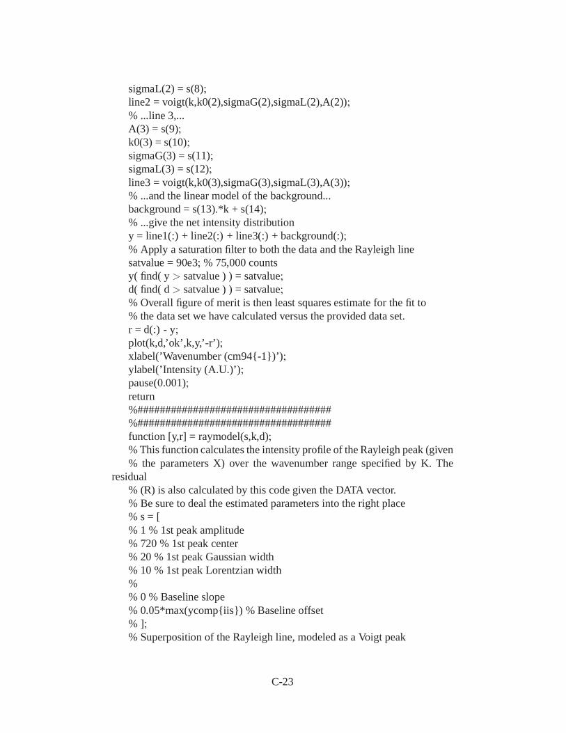
sigmaL(2) = s(8);line2 = voigt(k,k0(2),sigmaG(2),sigmaL(2),A(2));% ...line 3,...A(3) = s(9);k0(3) = s(10);sigmaG(3) = s(11);sigmaL(3) = s(12);line3 = voigt(k,k0(3),sigmaG(3),sigmaL(3),A(3));% ...and the linear model of the background...background = s(13).*k + s(14);% ...give the net intensity distributiony = line1(:) + line2(:) + line3(:) + background(:);% Apply a saturation filter to both the data and the Rayleigh linesatvalue = 90e3; % 75,000 countsy( find( y > satvalue ) ) = satvalue;d( find( d > satvalue ) ) = satvalue;% Overall figure of merit is then least squares estimate for the fit to% the data set we have calculated versus the provided data set.r = d(:) - y;plot(k,d,’ok’,k,y,’-r’);xlabel(’Wavenumber (cm94-1)’);ylabel(’Intensity (A.U.)’);pause(0.001);return%###################################%###################################function [y,r] = raymodel(s,k,d);% This function calculates the intensity profile of the Rayleigh peak (given% the parameters X) over the wavenumber range specified by K. The
residual% (R) is also calculated by this code given the DATA vector.% Be sure to deal the estimated parameters into the right place% s = [% 1 % 1st peak amplitude% 720 % 1st peak center% 20 % 1st peak Gaussian width% 10 % 1st peak Lorentzian width%% 0 % Baseline slope% 0.05*max(ycompiis) % Baseline offset% ];% Superposition of the Rayleigh line, modeled as a Voigt peak
C-23
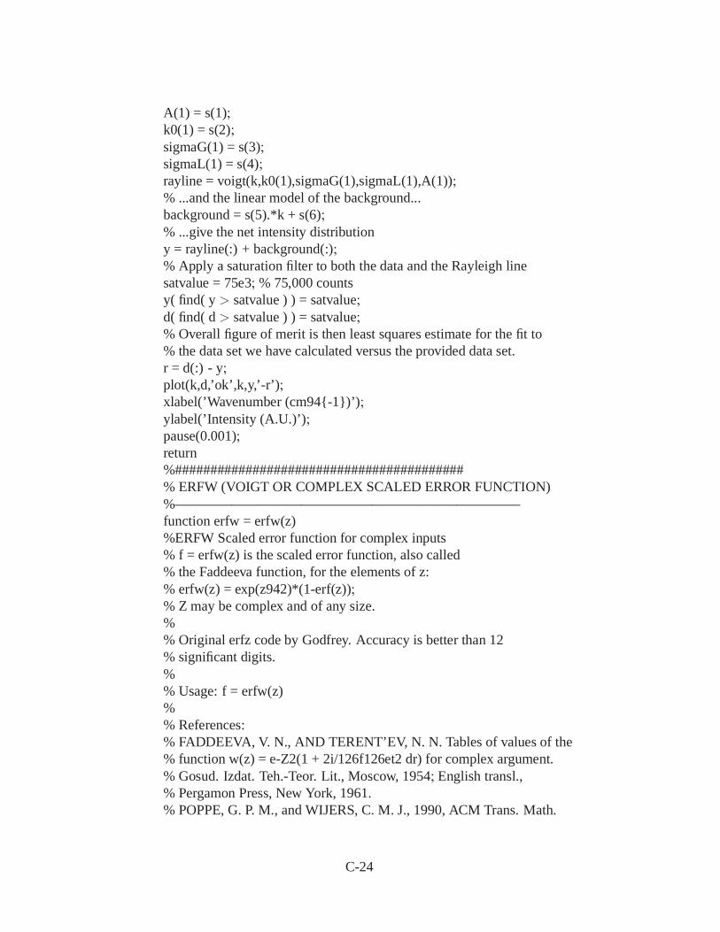
A(1) = s(1);k0(1) = s(2);sigmaG(1) = s(3);sigmaL(1) = s(4);rayline = voigt(k,k0(1),sigmaG(1),sigmaL(1),A(1));% ...and the linear model of the background...background = s(5).*k + s(6);% ...give the net intensity distributiony = rayline(:) + background(:);% Apply a saturation filter to both the data and the Rayleigh linesatvalue = 75e3; % 75,000 countsy( find( y > satvalue ) ) = satvalue;d( find( d > satvalue ) ) = satvalue;% Overall figure of merit is then least squares estimate for the fit to% the data set we have calculated versus the provided data set.r = d(:) - y;plot(k,d,’ok’,k,y,’-r’);xlabel(’Wavenumber (cm94-1)’);ylabel(’Intensity (A.U.)’);pause(0.001);return%#########################################% ERFW (VOIGT OR COMPLEX SCALED ERROR FUNCTION)%————————————————————————–function erfw = erfw(z)%ERFW Scaled error function for complex inputs% f = erfw(z) is the scaled error function, also called% the Faddeeva function, for the elements of z:% erfw(z) = exp(z942)*(1-erf(z));% Z may be complex and of any size.%% Original erfz code by Godfrey. Accuracy is better than 12% significant digits.%% Usage: f = erfw(z)%% References:% FADDEEVA, V. N., AND TERENT’EV, N. N. Tables of values of the% function w(z) = e-Z2(1 + 2i/126f126et2 dr) for complex argument.% Gosud. Izdat. Teh.-Teor. Lit., Moscow, 1954; English transl.,% Pergamon Press, New York, 1961.% POPPE, G. P. M., and WIJERS, C. M. J., 1990, ACM Trans. Math.
C-24
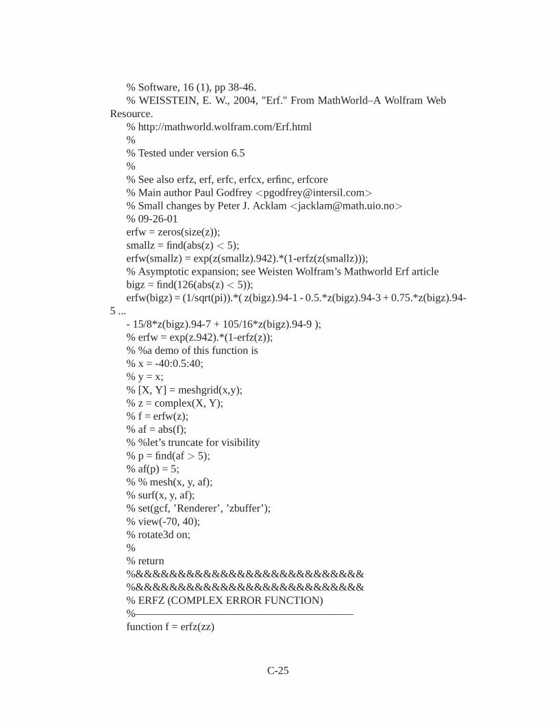
% Software, 16 (1), pp 38-46.% WEISSTEIN, E. W., 2004, "Erf." From MathWorld–A Wolfram Web
Resource.% http://mathworld.wolfram.com/Erf.html%% Tested under version 6.5%% See also erfz, erf, erfc, erfcx, erfinc, erfcore% Main author Paul Godfrey <[email protected]>% Small changes by Peter J. Acklam <[email protected]>% 09-26-01erfw = zeros(size(z));smallz = find(abs(z) < 5);erfw(smallz) = exp(z(smallz).942).*(1-erfz(z(smallz)));% Asymptotic expansion; see Weisten Wolfram’s Mathworld Erf articlebigz = find(126(abs(z) < 5));erfw(bigz) = (1/sqrt(pi)).*( z(bigz).94-1 - 0.5.*z(bigz).94-3 + 0.75.*z(bigz).94-
5 ...- 15/8*z(bigz).94-7 + 105/16*z(bigz).94-9 );% erfw = exp(z.942).*(1-erfz(z));% %a demo of this function is% x = -40:0.5:40;% y = x;% [X, Y] = meshgrid(x,y);% z = complex(X, Y);% f = erfw(z);% af = abs(f);% %let’s truncate for visibility% p = find(af > 5);% af(p) = 5;% % mesh(x, y, af);% surf(x, y, af);% set(gcf, ’Renderer’, ’zbuffer’);% view(-70, 40);% rotate3d on;%% return%&&&&&&&&&&&&&&&&&&&&&&&&&&&%&&&&&&&&&&&&&&&&&&&&&&&&&&&% ERFZ (COMPLEX ERROR FUNCTION)%————————————————————function f = erfz(zz)
C-25

%ERFZ Error function for complex inputs% f = erfz(z) is the error function for the elements of z.% Z may be complex and of any size.% Accuracy is better than 12 significant digits.%% Usage: f = erfz(z)%% Ref: Abramowitz & Stegun section 7.1% equations 7.1.9, 7.1.23, and 7.1.29%% Tested under version 5.3.1%% See also erf, erfc, erfcx, erfinc, erfcore% Main author Paul Godfrey <[email protected]>% Small changes by Peter J. Acklam <[email protected]>% 09-26-01error(nargchk(1, 1, nargin));% quick exit for empty inputif isempty(zz)f = zz;return;endtwopi = 2*pi;sqrtpi=1.772453850905516027298;f = zeros(size(zz));ff=f;az=abs(zz);p1=find(az<=8);p2=find(az> 8);if 126isempty(p1)z=zz(p1);nn = 32;x = real(z);y = imag(z);k1 = 2 / pi * exp(-x.*x);k2 = exp(-i*2*x.*y);s1 = erf(x);s2 = zeros(size(x));k = x 126= 0;% when x is non-zeros2(k) = k1(k) ./ (4*x(k)) .* (1 - k2(k));k = 126k;% when x is zeros2(k) = i / pi * y(k);
C-26
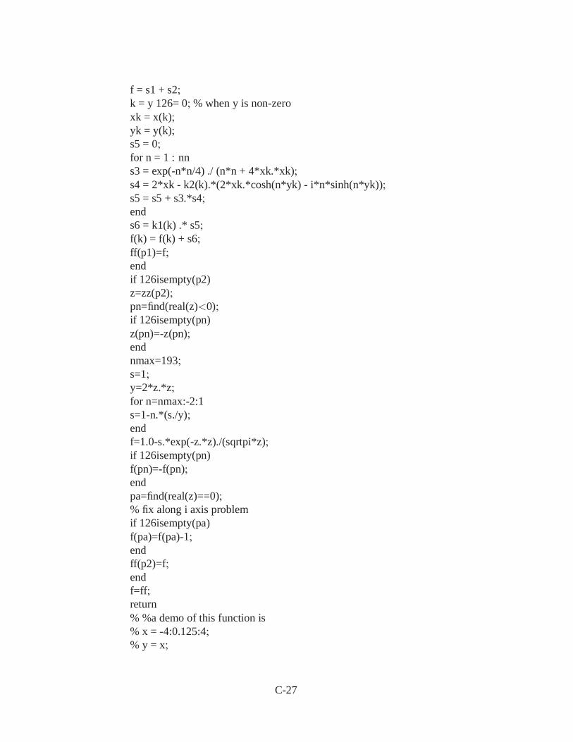
f = s1 + s2;k = y 126= 0;% when y is non-zeroxk = x(k);yk = y(k);s5 = 0;for n = 1 : nns3 = exp(-n*n/4) ./ (n*n + 4*xk.*xk);s4 = 2*xk - k2(k).*(2*xk.*cosh(n*yk) - i*n*sinh(n*yk));s5 = s5 + s3.*s4;ends6 = k1(k) .* s5;f(k) = f(k) + s6;ff(p1)=f;endif 126isempty(p2)z=zz(p2);pn=find(real(z)<0);if 126isempty(pn)z(pn)=-z(pn);endnmax=193;s=1;y=2*z.*z;for n=nmax:-2:1s=1-n.*(s./y);endf=1.0-s.*exp(-z.*z)./(sqrtpi*z);if 126isempty(pn)f(pn)=-f(pn);endpa=find(real(z)==0);% fix along i axis problemif 126isempty(pa)f(pa)=f(pa)-1;endff(p2)=f;endf=ff;return% %a demo of this function is% x = -4:0.125:4;% y = x;
C-27
% [X, Y] = meshgrid(x,y);% z = complex(X, Y);% f = erfz(z);% af = abs(f);% %let’s truncate for visibility% p = find(af > 5);% af(p) = 5;% mesh(x, y, af);% view(-70, 40);% rotate3d on;%% return%&&&&&&&&&&&&&&&&&&&&&&&&&&&%%% % STOKES LINES% k = kscan(a:b,1);% d = dscan(a:b,1);%% % Estimate the noise in the sample from the 10 pts near the ends% idx = 10;% sigmad = std([d(1:idx,1);d(end-idx:end)]);% bgoff = mean([d(1:idx,1);d(end-idx:end)]);% background offset% Rd = 1./sigmad;% pkpos = kr(floor(mean(find(d == max(d))))); % finds middle of flat
peak% pkAII = max(d); % strong STO x=1/3 peak% pkAI = 0.4*pkAII;% pkAIII = 0.1*pkAII;%%% % Set initial guesses and optimization parameters for RAMAN PEAKS% params = % % MIN MAX S(1) S(0) SIGMAS0 NAME% % Stokes line I – 766 STO (x = 1)% 0 1e6 pkAI pkAI Inf ’Stokes I [STO,x=1] line amplitude’% kminr kmaxr 766 766 03 ’Stokes I [STO,x=1] line center wavenumber’% 0 50 5 4 Inf ’Stokes I [STO,x=1] line Gaussian width’% 0 50 1 1 Inf ’Stokes I [STO,x=1] line Lorentzian width’% % Stokes line II – 788 STO (x = 1/3)% 0 1e6 pkAII pkAII Inf ’Stokes II [STO,x=1/3] line amplitude’
C-28
% kminr kmaxr 788 788 03 ’Stokes II [STO,x=1/3] line center wavenum-ber’
% 0 50 5 4 Inf ’Stokes II [STO,x=1/3] line Gaussian width’% 0 50 1 1 Inf ’Stokes II [STO,x=1/3] line Lorentzian width’% % Stokes line III – 796 STO (x = 0)% 0 1e6 pkAIII pkAIII Inf ’Stokes III [STO,x=0] line amplitude’% kminr kmaxr 796 796 03 ’Stokes III [STO,x=0] line center wavenum-
ber’% 0 50 5 4 Inf ’Stokes III [STO,x=0] line Gaussian width’% 0 50 1 1 Inf ’Stokes III [STO,x=0] line Lorentzian width’% % Background% -Inf Inf 0 0 1 ’Stokes line background slope’% -Inf Inf bgoff bgoff 0.1*bgoff ’Stokes line background offset’% ;%%%% sminiis,isn = cell2mat(params(:,1));% smaxiis,isn = cell2mat(params(:,2));% Ns = length(sminiis,isn);% if iis == 1% s1iis,isn = cell2mat(params(:,3));% else% s1iis,isn = shatiis-1;% end% s0iis,isn = cell2mat(params(:,4));% Rs0iis,isn = 1./(cell2mat(params(:,5)));% snameiis,isn = char(params(:,6));%% % Use MARQUARDT function% tic;% % [X, info, perf] = marquardt(fun, x0, opts, p1,p2,...)% % [fvec,dfds] = Rayleigh_LSQ_obj_func(s,k,d,Rdvec,s0r,Rs0vec);% [straceiis,isn, infoiis,isn, perfiis,isn] = marquardt...(@LSQ_obj_func,s1iis,isn...,opts,@linemodel,k,d,Rd,s0iis,isn,Rs0iis,isn,Npeaks);% toc;% shatiis,isn = straceiis,isn(:,end);% [fhatiis,isn,Jhatiis,isn] = LSQ_obj_func(shatiis,isn,@linemodel,k,d...,Rd,s0iis,isn,Rs0iis,isn,Npeaks);% % Perform error analysis% lastwarn(”);% clear all warnings
C-29

% % Mean square error for a MAP estimator is...% MSEiis,isn = inv( Jhatiis,isn(1:end-Nsr,:).’*Jhatiis,isn(1:end-Nsr,:)
+ ...% diag(Rs0iis,isn).’*diag(Rs0iis,isn) );% if 126strcmp(lastwarn,”);% try% disp(sprintf(’MSE is not well-conditioned: %g’,cond(MSE)));% catch% try% MSEiis,isn = pinv( Jhatiis,isn(1:end-Nsr,:).’*Jhatiis,isn(1:end-
Nsr,:) + ...% diag(Rs0iis,isn).’*diag(Rs0iis,isn) );% catch% MSEiis,isn = zeros(Ns,Ns);% end% end% end% scaled_covarianceiis,isn = MSEiis,isn;% sigmashatiis,isn = diag(sqrt(MSEiis,isn));% for is = 1:Ns;% scaled_covarianceiis,isn(is,:) = scaled_covarianceiis,isn(is,:).../sigmashatiis,isn(is);% scaled_covarianceiis,isn(:,is) = scaled_covarianceiis,isn(:,is).../sigmashatiis,isn(is);% end% % Report estimation results% for is = 1:Ns% disp(sprintf(’%s = %g +/- %g; s(1) = %g.’,deblank(snameiis,isn(is,:))...,shatiis,isn(is),sigmashatiis,isn(is),s1iis,isn(is)));% end% %_LINE_1__LINE_1__LINE_1__LINE_1__%%%%% % Peak centers are in 2 and 6... shift is then shat1(2)-shat2+(2)
etc.% kramanshift1iis,isn = shatiis,isn(2) - shat1,1(2);% disp(sprintf(’Shift for 1st peak from scan %g from %s is %g’...,isn,filenameiis,kramanshift1iis,isn));% kramanshift2iis,isn = shatiis,isn(6) - shat1,1(6);% disp(sprintf(’Shift for 2nd peak from scan %g from %s is %g’...
C-30
,isn,filenameiis,kramanshift2iis,isn));% kramanshift3iis,isn = shatiis,isn(10) - shat1,1(10);% disp(sprintf(’Shift for 3rd peak from scan %g from %s is %g’...,isn,filenameiis,kramanshift2iis,isn));% disp(’ ’);%%% % PLOT THE INFORMATION% switch scantypeiis% case ’point’% % No plots% case ’xline’% % PLOT% Nx = Nxscanposiis;% for ix = 1:Nx% xx(ix) = xscaniis,ix;% raman1(ix) = kramanshift1iis,ix;% raman2(ix) = kramanshift2iis,ix;% raman3(ix) = kramanshift3iis,ix;% end% figure;% plot(xx,raman1,xx,raman2,xx,raman3);% xlabel(’x (\it\mu\rmm)’);% ylabel(’Raman shift (cm94-1)’);% title(filenameiis,’Interpreter’,’none’);% case ’yline’% Ny = Nyscanposiis;% for iy = 1:Ny% yy(iy) = yscaniis,iy;% raman1(iy) = kramanshift1iis,iy;% raman2(iy) = kramanshift2iis,iy;% raman3(iy) = kramanshift3iis,iy;% end% figure;% plot(yy,raman1,yy,raman2,yy,raman3);% xlabel(’x (\it\mu\rmm)’);% ylabel(’Raman shift (cm94-1)’);% title(filenameiis,’Interpreter’,’none’);% case ’area’% Nx = Nxscanposiis;% Ny = Nyscanposiis;% for ix = 1:Nx
C-31

% for iy = 1:Ny% isn = iy + (ix-1)*Ny% xx(iy,ix) = xscaniis,isn;% yy(iy,ix) = yscaniis,isn;% raman1(iy,ix) = kramanshift1iis,isn;% raman2(iy,ix) = kramanshift2iis,isn;% raman3(iy,ix) = kramanshift3iis,isn;% end% end% figure;% surf(xx,yy,raman1);% xlabel(’x (\it\mu\rmm)’);% ylabel(’y (\it\mu\rmm)’);% zlabel(’Raman shift (cm94-1)’);% title(filenameiis,’Interpreter’,’none’);% end
C-32
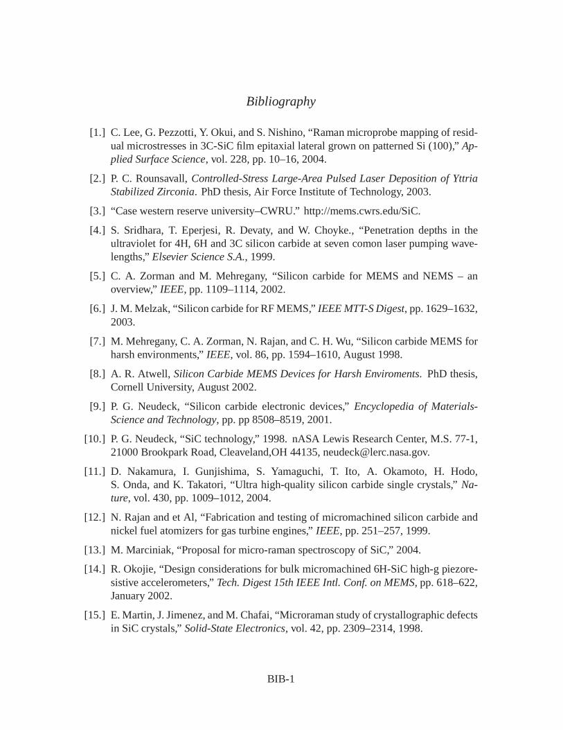
Bibliography
[1.] C. Lee, G. Pezzotti, Y. Okui, and S. Nishino, “Raman microprobe mapping of resid-ual microstresses in 3C-SiC film epitaxial lateral grown on patterned Si (100),” Ap-plied Surface Science, vol. 228, pp. 10–16, 2004.
[2.] P. C. Rounsavall, Controlled-Stress Large-Area Pulsed Laser Deposition of YttriaStabilized Zirconia. PhD thesis, Air Force Institute of Technology, 2003.
[3.] “Case western reserve university–CWRU.” http://mems.cwrs.edu/SiC.
[4.] S. Sridhara, T. Eperjesi, R. Devaty, and W. Choyke., “Penetration depths in theultraviolet for 4H, 6H and 3C silicon carbide at seven comon laser pumping wave-lengths,” Elsevier Science S.A., 1999.
[5.] C. A. Zorman and M. Mehregany, “Silicon carbide for MEMS and NEMS – anoverview,” IEEE, pp. 1109–1114, 2002.
[6.] J. M. Melzak, “Silicon carbide for RF MEMS,” IEEE MTT-S Digest, pp. 1629–1632,2003.
[7.] M. Mehregany, C. A. Zorman, N. Rajan, and C. H. Wu, “Silicon carbide MEMS forharsh environments,” IEEE, vol. 86, pp. 1594–1610, August 1998.
[8.] A. R. Atwell, Silicon Carbide MEMS Devices for Harsh Enviroments. PhD thesis,Cornell University, August 2002.
[9.] P. G. Neudeck, “Silicon carbide electronic devices,” Encyclopedia of Materials-Science and Technology, pp. pp 8508–8519, 2001.
[10.] P. G. Neudeck, “SiC technology,” 1998. nASA Lewis Research Center, M.S. 77-1,21000 Brookpark Road, Cleaveland,OH 44135, [email protected].
[11.] D. Nakamura, I. Gunjishima, S. Yamaguchi, T. Ito, A. Okamoto, H. Hodo,S. Onda, and K. Takatori, “Ultra high-quality silicon carbide single crystals,” Na-ture, vol. 430, pp. 1009–1012, 2004.
[12.] N. Rajan and et Al, “Fabrication and testing of micromachined silicon carbide andnickel fuel atomizers for gas turbine engines,” IEEE, pp. 251–257, 1999.
[13.] M. Marciniak, “Proposal for micro-raman spectroscopy of SiC,” 2004.
[14.] R. Okojie, “Design considerations for bulk micromachined 6H-SiC high-g piezore-sistive accelerometers,” Tech. Digest 15th IEEE Intl. Conf. on MEMS, pp. 618–622,January 2002.
[15.] E. Martin, J. Jimenez, and M. Chafai, “Microraman study of crystallographic defectsin SiC crystals,” Solid-State Electronics, vol. 42, pp. 2309–2314, 1998.
BIB-1
[16.] L. Starman, Characterization of Residual Stress in Microelectromechanical Systems(MEMS) Devices Using Raman Spectroscopy. PhD thesis, Air Force Institute ofTechnology, April 2002.
[17.] J. R. Ferraro and K. Nakamoto, Introductory Raman Spectroscopy. Academic Press,1994.
[18.] D. J. Brink, T. Maurice, S. Blanque, H. Kunert, J. Camassel, and J. Pascul, “Depthprofiling of high-energy hydrogen-impanted 6H-SiC,” Applied Optics, vol. 43, no. 6,pp. 1275–1280, 20 February 2004.
[19.] “What is silicon carbide?,” tech. rep., NASA Jet Propulsion Labratory, January2003. http://vshields.jpl.nasa.gov/SiC/CubicHex.html.
[20.] S. Sze, Semiconductor Devices: Physics and Technology. John Wiley & Sons, 2002.
[21.] M. E. Zvanut, “Electron paramagnetic resonance of electronic-grade SiC sub-strates,” Journal of Physics: Condensded Matter, vol. 16, pp. 1341–1367, 2004.
[22.] B. El-Kareh, Fundamentals of Semiconductors Processing Technologies. Boston:Kluwer Academic, 1995.
[23.] C. A. Wert and R. M. Thomson, Physics of Solids. McGraw-Hill, 1964.
[24.] R. Madar, “Silicon carbide in contention,” Nature, vol. 430, pp. 974–975, 2004.
[25.] D. W. Feldman, J. H. Parker, W. Choyke, and L. Patrick, “Raman scattering in 6H-SiC,” Physical Review, vol. 170, no. 3, pp. 698–704, 15 June 1968.
[26.] T.Tomoita, S.Saito, M.Baba, M. Hundhusen, T. Suemoto, and S. Nakashima, “Se-lective resonace effects of the folded longitudinal phonon modes in the raman spec-tra of SiC,” Physical Review B, vol. 62, 15 November 2000.
[27.] S. Ferrero and et al, “Defect characterization of 4H-SiCwafers for power electronic device applications,” January 2003.http://www2.polito.it/research/thinfims/papers/Bo_def.pdf.
[28.] J. Liu and Y. K. Vohra, “Raman modes of 6H polytype of silicon carbide to ultrahighpressures: A comparison with silicon and diamond,” Physical review letters, vol. 72,pp. 4105–4108, 27 June 1994.
[29.] S. Rohmfeld, M. Hundhausen, and L. Ley, “Raman scattering in polycrystalline3C-SiC: Influence of stacking faults,” Physical Review B, vol. 58, no. 15, pp. 9858–9862, 15 October 1998.
[30.] K. Bradley, J. Foley, A. Cash, S. Roberson, A. Beliveau, and R. Okojie, “Tesingand analysis of piezoresistive signals from silicon carbide MEMS accelerometerswith application to penetration fuzing,” Air Force Research Labs,Applied RasearchAssociates,NASA Glenn Research Center, NDIA Fuze Conference-Charlotte, NC,2004.
BIB-2
[31.] J. Foley. Personal Correspondance, Air Force Munitions Labratory; Muntions Di-rectorate Fuzes Branch (AFRL/MNMF), [email protected].
[32.] Cree Inc, Silicon Carbide Substrates, 1998. Product Specifications: 4H SiliconCarbide (n/p-type, Semi-Insulating); 6H Silicon Carbide (n/p-type).
[33.] M. E. Levinshtein, S. L. Rumyantsev, and M. S. Shur, Properties of Advanced Semi-conductor Material: GaN, AlN, InN, BN, SiC, SiGe. John Wiley & Sons, 2001.
[34.] Wolfe, Holonyak, and Stillman, Physical Properties of Semiconductors.
[35.] P. E. Kladitis, “EENG 596 intergrated ciruit technology lecture notes,” Fall 2003.Midterm Soln. to Problem #3.
[36.] J. Melzak. Flx Microweb site: www.flxmicro.com.
[37.] Http://Www.Cp.Umist.Ac.Uk/CPC/Facilities/Electron, “Corrosion & protectioncentre: Research facilities:scanning electron microscopy.”
[38.] Z. Corporation, NewView 5000 Operating Manual OMP-0423H, 2002.
[39.] S. Ness, “Stress analysis of silicon carbide microelectromechanical systems(MEMS) devices using raman spectroscopy,” Master’s thesis, Air Force Instituteof Technology, March 2003.
[40.] V. Micro-Measurements, Model P3 Strain Indicator and Recorder: InstructionManual. Vishay Micro-Measurements P.O. Box 27777 Raleigh, NC 27611 USATelephone: (919) 365-3800 Facsimile: (919) 365-3945 [email protected], September 2003.
[41.] W. Sharp, B. Yuan, R. Vaidyanathan, and R. Edwards, “Measurements of young’smodulus, poisson’s ratio, and the tensile strength of polysilicon,” Proceedings of theTenth Annual Workshop of Micro Electro Mechanical Systems, pp. 424–429, 1997.
[42.] J. S. Milton and J. C. Arnold, Introduction to Probability and Statistics Principlesand Application for Engineering and the Computing Sciences. New York, NewYork: McGraw Hill, 2003.
[43.] D. Petrosky, “Personal correspondence.” Suggestion that Nuclear Radiation couldrelieve stress in SiC, 2004.
[44.] H. R. Philipp and E. Taft, Silicon Carbide – a High Temperature Semiconductor.Oxford: Pergamon Press, 1960.
[45.] E. I. Radovanova, Ph.D. Thesis. PhD thesis, The Ioffe Institute of Russian Academyof Science, 1970.
[46.] L. Patrick and W. Choyke, “Optical absorption in n-type cubic SiC,” Physical Re-view, vol. 186, pp. 775–777, 15 October 1969.
[47.] C. Persson and U. Lindefelt, “Relativistic band structure calculation of cubic andhexagonal SiC polytypes,” J. Appl. Phys., pp. 5496–5508., 1997.
BIB-3

REPORT DOCUMENTATION PAGE Form ApprovedOMB No. 0704-0188
1. REPORT DATE (DD-MM-YYYY)22-03-2005
2. REPORT TYPE Master's Thesis
4. TITLE AND SUBTITLEDetection of Residual Stress in SiC MEMS Using µ-Raman Spectroscopy
5a. CONTRACT NUMBER
6. AUTHOR(S)Zingarelli,John,C. 1Lt USAF
7. PERFORMING ORGANIZATION NAME(S) AND ADDRESS(ES)Air Force Institute of Technology, Graduate School of Engineering and Management (AFIT/EN), 2950 Hobson Way, WPAFB OH 45433-7765.
9. SPONSORING/MONITORING AGENCY NAME(S) AND ADDRESS(ES)Jason R. Foley, Mechanical Engineer AFRL/MNMF 306 W. Eglin Blvd., Bldg 432 Eglin AFB, FL 32542-5430
8. PERFORMING ORGANIZATION REPORT NUMBER
AFIT/GEO/ENP/05-06
10. SPONSOR/MONITOR'S ACRONYM(S)
13. SUPPLEMENTARY NOTES
12. DISTRIBUTION/AVAILABILITY STATEMENTAPPROVED FOR PUBLIC RELEASE; DISTRIBUTION UNLIMITED
14. ABSTRACTMicro-Raman (µ-Raman) spectroscopy is used to measure residual stress in two silicon carbide (SiC) poly-types: single-crystal,hexagonally symmetric 6H-SiC, and polycrystalline, cubic 3C-SiC thin films deposited on Si substrates. Both are used inmicro-electrical-mechanical systems (MEMS) devices. By employing an incorporated piezoelectric stage with submicronpositioning capabilities along with the Raman spectral acquisition, spatial scans are performed to reveal areas in the 6H-SiCMEMS structures that contain residual stress. Shifts in the transverse optical (TO) Stokes peaks of up to 2 cm^-1 are correlated tothe material strain induced by the MEMS fabrication process through the development of phonon deformation potential curves forthis material. The 3C-SiC films, with thicknesses ranging from 1.5-5 µm, are deposited by CVD on (100) Si substrates and arealso investigated to determine their residual stress. An ultraviolet excitation source (v = 325 nm, hv = 3.82 eV) was determinedto be more effective for the detection of Raman shifts in these thin films than the 514-nm source, since the absorption coefficient inSiC at 300 K at 325 nm is 3660 cm-1, while that at 514 nm is less than 100 cm-1.
15. SUBJECT TERMSMicro-electro-mechanical Systems, MEMS, Raman Spectroscopy, Silicon Carbide, 3C-SiC, 6H-SiC, Residual Stress
18. NUMBER OF PAGES
137
19a. NAME OF RESPONSIBLE PERSON Marciniak, Michael A Civ AFIT/ENP a. REPORT
Ub. ABSTRACT
Uc. THIS PAGE
U
17. LIMITATION OF ABSTRACT
UU
Standard Form 298 (Rev. 8/98)Prescribed by ANSI Std. Z39.18
PLEASE DO NOT RETURN YOUR FORM TO THE ABOVE ORGANIZATION. 3. DATES COVERED (From - To)
Feb 2004-Mar 2005
5b. GRANT NUMBER
5c. PROGRAM ELEMENT NUMBER
5d. PROJECT NUMBER
5e. TASK NUMBER
5f. WORK UNIT NUMBER
11. SPONSOR/MONITOR'S REPORT NUMBER(S)
16. SECURITY CLASSIFICATION OF:
19b. TELEPHONE NUMBER (Include area code)(937)255-3636 ext.4529
The public reporting burden for this collection of information is estimated to average 1 hour per response, including the time for reviewing instructions, searching existing data sources,gathering and maintaining the data needed, and completing and reviewing the collection of information. Send comments regarding this burden estimate or any other aspect of this collectionof information, including suggestions for reducing the burden, to the Department of Defense, Executive Services and Communications Directorate (0704-0188). Respondents should be awarethat notwithstanding any other provision of law, no person shall be subject to any penalty for failing to comply with a collection of information if it does not display a currently valid OMBcontrol number.