Embed Size (px)
Citation preview

Raman Spectroscopy of GrapheneApplications in Epitaxial Graphene/SiC
MVS Chandrashekhar
Department of Electrical EngineeringUniversity of South Carolina
Columbia, SC 29208

Outline• Introduction• The Raman Effect• Phonons in Crystals• Raman Spectra of Carbon Materials– Double Resonant D-peak
• Raman Spectrum of Graphene• Raman Spectrum of Epitaxial Graphene– Applications
• Conclusion
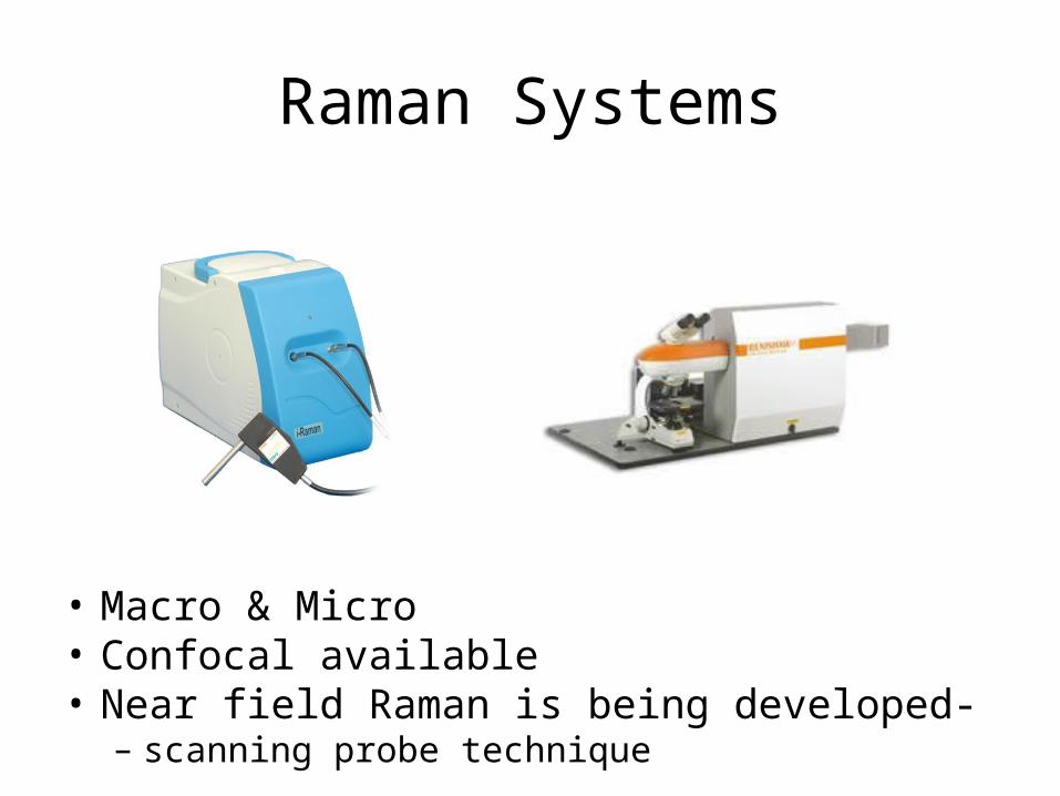
Raman Systems
• Macro & Micro• Confocal available• Near field Raman is being developed-– scanning probe technique
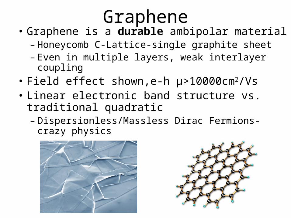
Graphene• Graphene is a durable ambipolar material– Honeycomb C-Lattice-single graphite sheet– Even in multiple layers, weak interlayer coupling
• Field effect shown,e-h µ>10000cm2/Vs• Linear electronic band structure vs. traditional
quadratic– Dispersionless/Massless Dirac Fermions-crazy physics
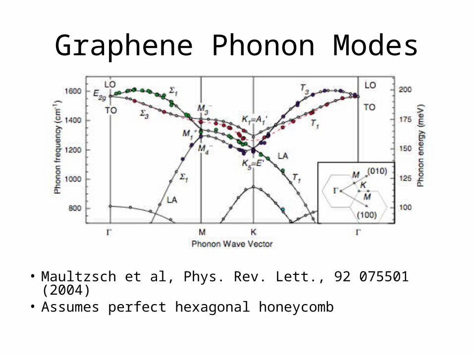
Graphene Phonon Modes
• Maultzsch et al, Phys. Rev. Lett., 92 075501 (2004)• Assumes perfect hexagonal honeycomb
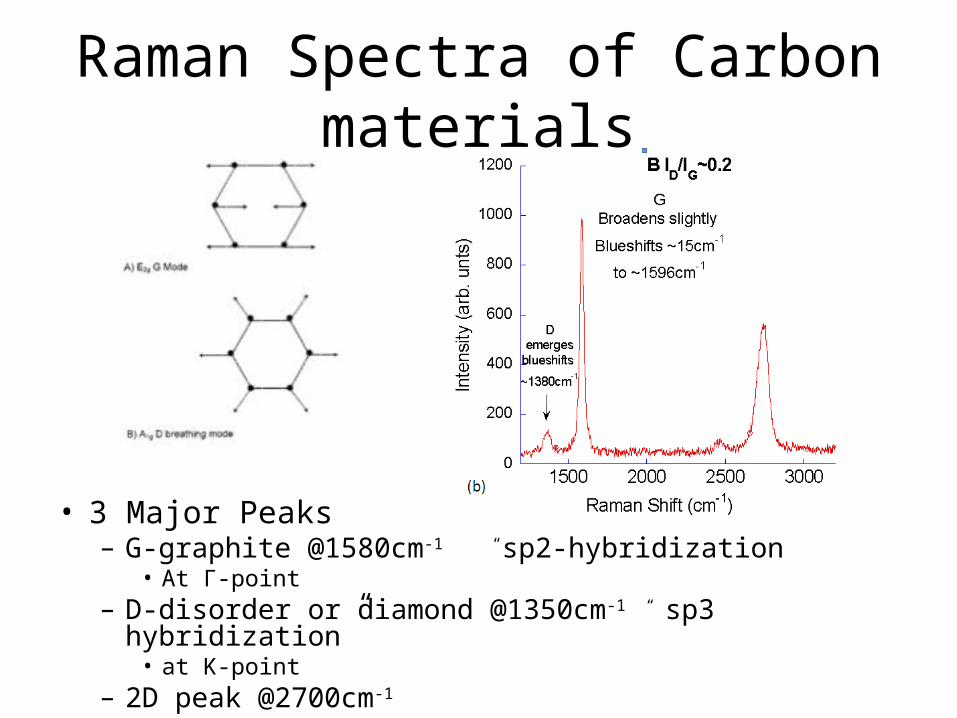
Raman Spectra of Carbon materials
• 3 Major Peaks– G-graphite @1580cm-1 “sp2-hybridization”
• At Γ-point– D-disorder or diamond @1350cm-1 “ sp3 hybridization”
• at K-point– 2D peak @2700cm-1
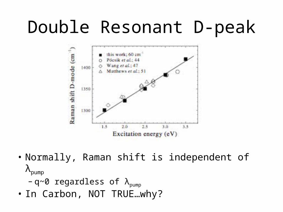
Double Resonant D-peak
• Normally, Raman shift is independent of λpump
– q~0 regardless of λpump
• In Carbon, NOT TRUE…why?
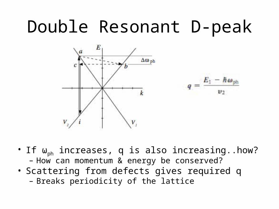
Double Resonant D-peak
• If ωph increases, q is also increasing..how?– How can momentum & energy be conserved?
• Scattering from defects gives required q– Breaks periodicity of the lattice

Identifying Carbon Allotropes
• Many different allotropes of carbon
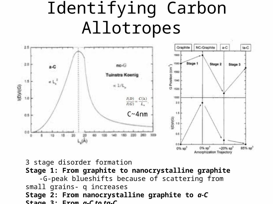
Identifying Carbon Allotropes
3 stage disorder formationStage 1: From graphite to nanocrystalline graphite
-G-peak blueshifts because of scattering from small grains- q increasesStage 2: From nanocrystalline graphite to a-CStage 3: From a-C to ta-C
C~4nm

Raman Spectrum of Graphene
• D-peak only at edges –”disorder”• 2D peak intensity changes with thickness
Graf et al. arxiv (2006)
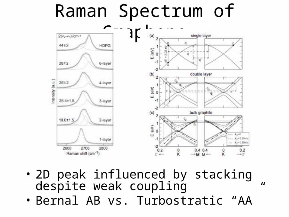
Raman Spectrum of Graphene
• 2D peak influenced by stacking despite weak coupling
• Bernal AB vs. Turbostratic “AA”
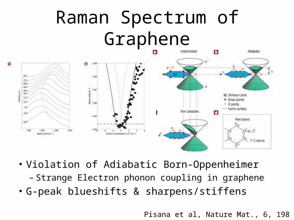
Raman Spectrum of Graphene
• Violation of Adiabatic Born-Oppenheimer– Strange Electron phonon coupling in graphene
• G-peak blueshifts & sharpens/stiffensPisana et al, Nature Mat., 6, 198 (2007)
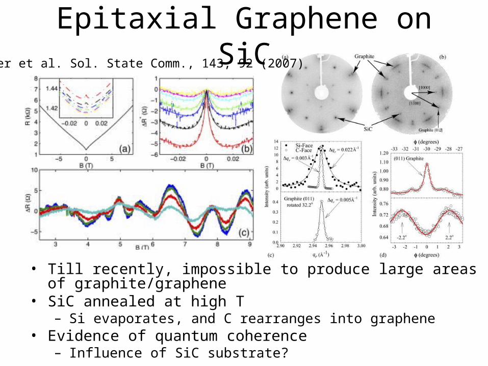
Epitaxial Graphene on SiC
• Till recently, impossible to produce large areas of graphite/graphene• SiC annealed at high T
– Si evaporates, and C rearranges into graphene• Evidence of quantum coherence
– Influence of SiC substrate?
De Heer et al. Sol. State Comm., 143, 92 (2007)

Epitaxial Graphene Growth
• 1300C-1600C, 15mins-60mins• C-face and Si-face • Vacuum in cold wall & Hot wall BP ~10-7 Torr• We will address general trends common in both
Cold Wall Hot Wall

Basic Material Properties
• Typical Si-face RT mobility ~1000cm2/Vs• Highest Si-face mobility > 5000cm2 /Vs at 120K

C-face vs. Si-face
• 2D peak is very different for the two– C-face turbostratic-single peak-looks like single layer as c-
axis symmetry is broken-Symmetric peak– Si-face Bernal stack-splits-Asymmetric peak
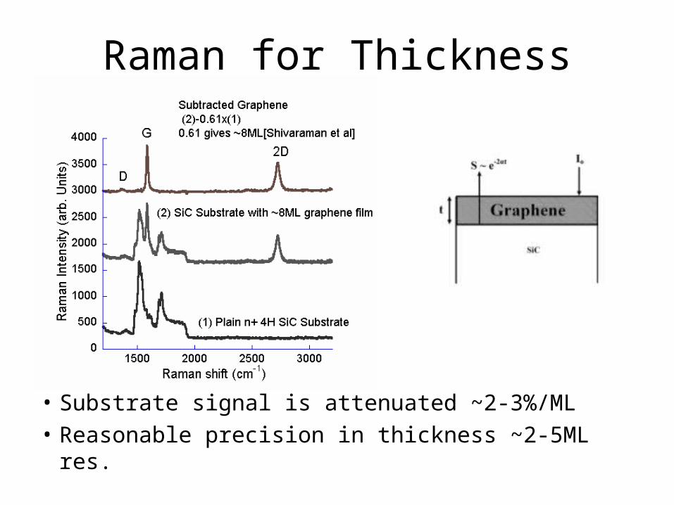
Raman for Thickness
• Substrate signal is attenuated ~2-3%/ML• Reasonable precision in thickness ~2-5ML res.
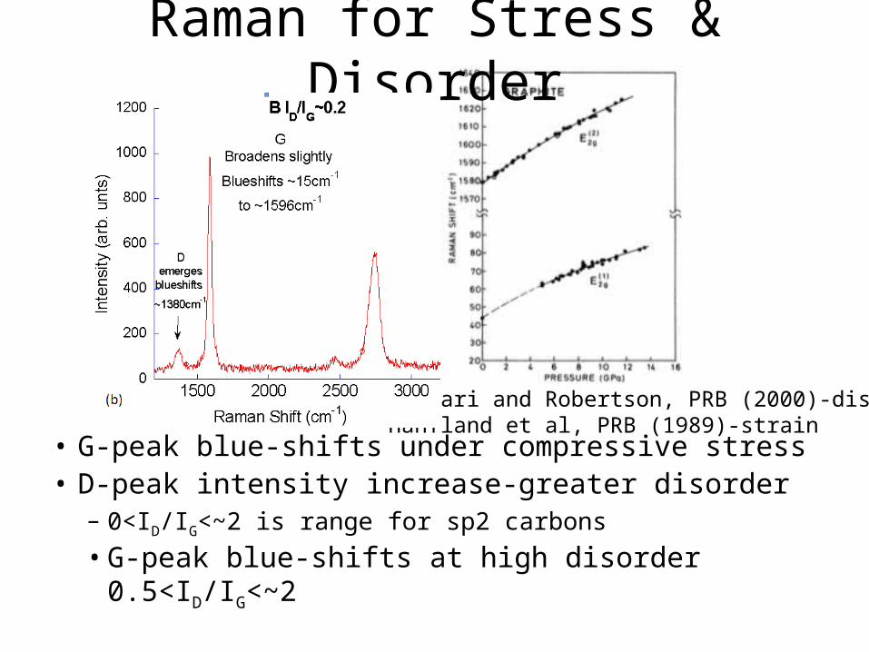
Raman for Stress & Disorder
• G-peak blue-shifts under compressive stress• D-peak intensity increase-greater disorder– 0<ID/IG<~2 is range for sp2 carbons
• G-peak blue-shifts at high disorder 0.5<ID/IG<~2
Ferrari and Robertson, PRB (2000)-disorderHanfland et al, PRB (1989)-strain

Stress & Disorder Cont.
• Two Major “Buckets”• I.Low disorder ID/IG<0.2, slow growth stress branch• III.High disorder, high growth ID/IG>0.5 disorder
branch– Stress relief believed to be through loss of registry

Stress & Disorder Branches• Stress Branch • Disorder branch
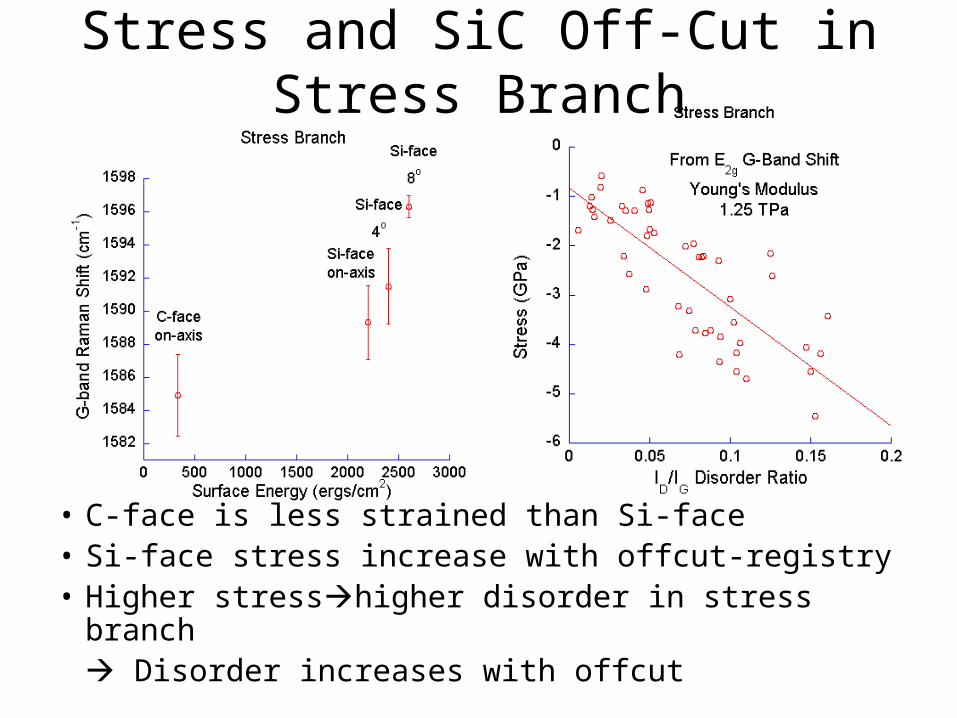
Stress and SiC Off-Cut in Stress Branch
• C-face is less strained than Si-face• Si-face stress increase with offcut-registry• Higher stresshigher disorder in stress branch
Disorder increases with offcut
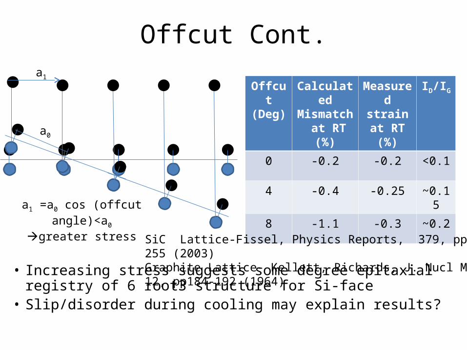
Offcut Cont.
• Increasing stress suggests some degree epitaxial registry of 6 root3 structure for Si-face
• Slip/disorder during cooling may explain results?
a0
a1
a1 =a0 cos (offcut angle)<a0
greater stress
Offcut (Deg)
Calculated Mismatch at RT (%)
Measured strain at RT (%)
ID/IG
0 -0.2 -0.2 <0.1
4 -0.4 -0.25 ~0.15
8 -1.1 -0.3 ~0.2
SiC Lattice-Fissel, Physics Reports, 379, pp149-255 (2003)Graphite Lattice- Kellett, Richards, J. Nucl Mat., 12, pp184-192 (1964)

Released Graphene Membranes
• Release gets rid of stress-no substrate• D-peak emerges-etch induced disorder?

Epitaxial Graphene Mobility
• Correlation 2D peak width and Hall mobilityRobinson et al, Nano Lett., 9, 2873 (2009)
Conclusions• Raman discovered by CV Raman• In crystals, shift is caused by lattice vibrations• Vibrations couple with electrons and EM fields• Large area graphene can be produced on SiC• Raman can completely characterize epitaxial
graphene– Thickness, stress, grain size, mobility, stacking

Questions?


![Electronic structure of epitaxial graphene layers on SiC ... to those found on exfoliated graphene [2, 3, 8, 9]. Besides being a more practical and scalable approach to 2D graphene](https://img.pdfslide.us/doc/110x75/5cb88a6988c993f5538b72ed/electronic-structure-of-epitaxial-graphene-layers-on-sic-to-those-found-on-exfoliated.jpg)