Embed Size (px)
Citation preview

Detection of Foreign Objectsin close proximity to an inductive charger
Master’s thesis in Master Programme Systems, Control and Mechatronics
PATRIC STRANDBERGKARL TAGEMAN
Department of Signals and SystemsCHALMERS UNIVERSITY OF TECHNOLOGYGothenburg, Sweden 2016


Master’s thesis 2016:EX070/2016
Detection of Foreign Objects
in close proximity to an inductive charger
PATRIC STRANDBERGKARL TAGEMAN
Department of Signals and SystemsChalmers University of Technology
Gothenburg, Sweden 2016

Detection of Foreign Objectsin close proximity to an inductive chargerPATRIC STRANDBERGKARL TAGEMAN
© PATRIC STRANDBERGKARL TAGEMAN, 2016.
Supervisor: CHRISTIAN EKMAN, QRTECHExaminer: TOMAS MCKELVEY, Signals and Systems
Master’s Thesis 2016:EX070/2016Department of Signals and SystemsChalmers University of TechnologySE-412 96 GothenburgTelephone +46 31 772 1000
iv
AbstractA prototype of a detection unit has been developed, constructed and evaluated. It iscapable of detecting live beings, as well as conductive objects. The area of applicationis together with an inductive charger and its purpose is to detect if live beings or con-ductive objects are too close to the inductive charger. The detection unit consists oftwo subsystems, one for each type of object. For live beings, ultrasonic sensors are usedand for conductive objects search coil sensors. The system is operational and can detectlive beings down to a width of approximately 10 cm and conductive objects the size ofa coin.
Keywords: Inductive Charging, Metal Detector, Search Coil Sensor, MagneticFields, Ultrasonic Sensors
v


AcknowledgementsWe want to thank QRTECH for the opportunity to do our Master Thesis there, andthe support and response they have provided during the entire project. We want togive a special thank to our supervisors, Christian Ekman and Carl Petterson for thevaluable support, help and feedback they have given us. Lastly we also want to thankour examiner Tomas McKelvey for the great input he provided.
Patric & KarlGothenburg, Sweden 2016
vii


Contents
1 Introduction 11.1 Background . . . . . . . . . . . . . . . . . . . . . . . . . . . . . . . . . . 11.2 Purpose . . . . . . . . . . . . . . . . . . . . . . . . . . . . . . . . . . . . 11.3 Problem Formulation . . . . . . . . . . . . . . . . . . . . . . . . . . . . . 2
1.3.1 Requirement Specification . . . . . . . . . . . . . . . . . . . . . . 21.4 Scope . . . . . . . . . . . . . . . . . . . . . . . . . . . . . . . . . . . . . 21.5 Method . . . . . . . . . . . . . . . . . . . . . . . . . . . . . . . . . . . . 2
2 Theory 52.1 Exposure to time-varying magnetic fields . . . . . . . . . . . . . . . . . . 5
2.1.1 Live Beings . . . . . . . . . . . . . . . . . . . . . . . . . . . . . . 52.1.2 Conductive Objects . . . . . . . . . . . . . . . . . . . . . . . . . . 5
2.2 Resonance . . . . . . . . . . . . . . . . . . . . . . . . . . . . . . . . . . . 62.2.1 Quality Factor . . . . . . . . . . . . . . . . . . . . . . . . . . . . . 8
3 Choice of Sensor Technologies 93.1 Detection of Live Beings . . . . . . . . . . . . . . . . . . . . . . . . . . . 93.2 Detection of Conductive Objects . . . . . . . . . . . . . . . . . . . . . . . 11
4 Design of Sensor Array 134.1 Ultrasonic . . . . . . . . . . . . . . . . . . . . . . . . . . . . . . . . . . . 13
4.1.1 Environment Protection in Final Production Version . . . . . . . 144.2 Search Coil Sensor . . . . . . . . . . . . . . . . . . . . . . . . . . . . . . 15
4.2.1 Basics . . . . . . . . . . . . . . . . . . . . . . . . . . . . . . . . . 154.2.2 Induction Balance . . . . . . . . . . . . . . . . . . . . . . . . . . . 154.2.3 Design Parameters . . . . . . . . . . . . . . . . . . . . . . . . . . 164.2.4 Operating Frequency . . . . . . . . . . . . . . . . . . . . . . . . . 184.2.5 Placement . . . . . . . . . . . . . . . . . . . . . . . . . . . . . . . 184.2.6 Input and Output . . . . . . . . . . . . . . . . . . . . . . . . . . . 19
5 Electronics Design 215.1 Power Supply . . . . . . . . . . . . . . . . . . . . . . . . . . . . . . . . . 225.2 Detection of Live Beings . . . . . . . . . . . . . . . . . . . . . . . . . . . 22
5.2.1 Ultrasonic Sensors . . . . . . . . . . . . . . . . . . . . . . . . . . 22
ix
Contents
5.2.2 Ultrasonic Receivers . . . . . . . . . . . . . . . . . . . . . . . . . 235.2.3 Peak Detectors . . . . . . . . . . . . . . . . . . . . . . . . . . . . 235.2.4 External ADC . . . . . . . . . . . . . . . . . . . . . . . . . . . . . 25
5.3 Detection of Conductive Objects . . . . . . . . . . . . . . . . . . . . . . . 265.3.1 Electronic Oscillator . . . . . . . . . . . . . . . . . . . . . . . . . 26
5.3.1.1 Choice of Frequency . . . . . . . . . . . . . . . . . . . . 275.3.1.2 Simulation . . . . . . . . . . . . . . . . . . . . . . . . . 28
5.3.2 Transmitter Amplifier . . . . . . . . . . . . . . . . . . . . . . . . 305.3.3 Transmitter Coils . . . . . . . . . . . . . . . . . . . . . . . . . . . 325.3.4 Receiver Coils . . . . . . . . . . . . . . . . . . . . . . . . . . . . . 345.3.5 Filter . . . . . . . . . . . . . . . . . . . . . . . . . . . . . . . . . . 365.3.6 Peak detector . . . . . . . . . . . . . . . . . . . . . . . . . . . . . 37
5.4 User and Charging Station alert . . . . . . . . . . . . . . . . . . . . . . . 385.5 MCU . . . . . . . . . . . . . . . . . . . . . . . . . . . . . . . . . . . . . . 38
5.5.1 TTL . . . . . . . . . . . . . . . . . . . . . . . . . . . . . . . . . . 395.5.2 Software Implementation . . . . . . . . . . . . . . . . . . . . . . . 40
5.6 PCB Layout . . . . . . . . . . . . . . . . . . . . . . . . . . . . . . . . . . 42
6 Results 456.1 Detection of Live Beings . . . . . . . . . . . . . . . . . . . . . . . . . . . 456.2 Detection of Conductive Objects . . . . . . . . . . . . . . . . . . . . . . . 48
6.2.1 Verification . . . . . . . . . . . . . . . . . . . . . . . . . . . . . . 486.2.1.1 Transmitter Side . . . . . . . . . . . . . . . . . . . . . . 486.2.1.2 Receiver Side . . . . . . . . . . . . . . . . . . . . . . . . 48
6.2.2 Current Measurement . . . . . . . . . . . . . . . . . . . . . . . . 496.2.3 Test of Search Coil Without Presence of Charge field . . . . . . . 506.2.4 Test of Search Coil With Presence of Charge field . . . . . . . . . 52
7 Discussion 557.1 Detection of Conductive Objects . . . . . . . . . . . . . . . . . . . . . . . 55
7.1.1 Colpitts Oscillator . . . . . . . . . . . . . . . . . . . . . . . . . . 567.1.2 Performance close to the inductive charger . . . . . . . . . . . . . 57
7.2 Detection of Live Beings . . . . . . . . . . . . . . . . . . . . . . . . . . . 57
8 Conclusion 59
Bibliography 61
A Appendix 1 I
x
1Introduction
This chapter covers the introduction of this project.
1.1 BackgroundWireless, or inductive charging, will be an important technology to facilitate a mass-adoption of electric vehicles. Wireless charging is easier to use compared to its coun-terpart - a power cord [1]. A wireless charging station can be installed in a garage andthe driver can simply park on top of the charging pad to initiate charging. It is alsopossible for the technology to be implemented in roads, allowing the car to be chargedwhile driving, effectively giving you unlimited range [2].
The batteries in electric vehicles have a very large capacity. To charge these ata reasonable rate, a large amount of power have to be transferred in a short amountof time. The strength of the magnetic field used is proportional to the transferredpower. This means that the magnetic field used for charging will be strong. To achievehigh efficiency, the field used will also have a high-frequency. A magnetic field withthese properties can be hazardous if unwanted conductive objects enter the field as eddycurrents will be induced in the objects. Highly conductive objects, such as metallicobjects, will be rapidly heated. This can cause both injury and material damage. Inliving beings the effect of the charging field will cause currents along nerves which cancause muscle spasms and, if the field is strong enough, even nerve damage. Accordingto the International Commission on Non-Ionizing Radiation guidelines [3] the limit forgeneral public exposure to magnetic fields is 6.25 µT in the frequency range 3−150kHz.This will be surpassed by the field generated by the charger.
It it is not feasible to fence in the dangerous space. Instead, detecting unwantedobjects entering the field, and then temporarily turning the field off, is a possible wayto make sure that inductive charging is safe.
1.2 PurposeThe purpose was to design and construct a prototype of a detection unit. It shouldbe capable of detecting conductive objects and live beings while in proximity to analternating high-strength magnetic field. The detection unit should also be able toinform the user and alert the charging station if an object has been detected.
1
1. Introduction
1.3 Problem FormulationThe main problem of this project was to design and construct a detection unit capableof detecting both live beings and conductive objects in a high frequency magnetic field.Detecting live beings and conductive objects were considered as two different problemswhich required different types of sensors. The electronics should be able to function inproximity to the charging station.
1.3.1 Requirement SpecificationThe requirement specification for a final version of the detection unit is listed below.Since the charging system that this project work with was incomplete, the specificationis based on preliminary information given by the designers of the charging station.
• Live beings equal or larger in size to a fist should be detected• The area of detection of living beings should be a square with length equal to the
inner width of a typical wheel-pair, approximately 1.3m.• Conductive objects should be detected before they are within the area where dan-
gerous heating can occur; i.e. between the sender and receiver coil of the chargingsystem.
• Conductive object equal or larger in size to a one SEK coin should be detected• The detection unit should be able to send a start/stop signal to the charging station• The detection unit should alert the user when charging has been stopped
1.4 ScopeThe detection unit is constructed for use in a laboratory environment. This means thatthe device is not going to be designed to be weather-resistant, or to survive being runover by a car. It will be tested together with the charging station although not at fullcapacity. Since this project will only develop a prototype of the detection unit it isnot required to cover the entire area in the specification. The requirement concerningsizes and communication should still be fulfilled by the prototype in the covered area.It should also be possible to extend the detection technologies used in the prototype tocover the entire area.
The project will assume to have access to a dc source with desired voltage. In theprototype this will be supplied through a dc power supply.
1.5 MethodA literature study was first carried out in order to get familiar with the topic andcurrent technologies. Different sensor technologies that already exists or can be appliedwas then evaluated using pros and cons in order to determine suitable ways of detectinglive beings as well as conductive objects. The needed electronics was designed and
2
1. Introduction
simulated using LTSpice, a software capable of simulating electric circuits. The circuitswas simultaneously verified and modified using prototypes in a trial and error fashionbefore the final version was constructed. The circuit board containing all the electronicswas created using Altium Designer. A microcontroller unit (MCU) was used to controlthe system and all its sensors. It was used to monitor the sensor readings and if adetection was reported communicate this to the charging station and user. The softwarewas written using the Arduino API, which is based on C code but has many built-inlibraries and functions which made the embedded programming more simple.
3

1. Introduction
4
2Theory
This chapter will list existing theory relevant to this master thesis.
2.1 Exposure to time-varying magnetic fieldsExposure to magnetic fields affect different kinds of materials differently depending ona number of factors. Among these are the frequency of the magnetic field and theconductivity and permeability of the material. This section will differentiate betweenthe effects caused to live beings and conductive objects.
2.1.1 Live BeingsLive beings have small amounts of currents running through them that occur naturallyas part of functions within the body. One well-known example is nerve signals whichconsist of small electrical impulses, but most biochemical reactions uses charged particlesin their functions [9]. A low frequency (LF) field, which is the designation for fields in therange of 30kHz − 300kHz, influence these charged particles through induced currents.A strong magnetic field implies a high induced current. If this current is strong enough,it is possible for it to stimulate nerves and muscles, and disturb other processes inthe body as well [9]. Another problem is energy absorption. All materials that areelectrically conductive, (which includes live beings) absorbs energy in the form of heatwhen exposed to alternating magnetic fields. For live beings this generally requiresfrequencies above 100kHz. The International Commission On Non-Ionizing RadiationProtection, (ICNIRP) has published guidelines concerning general public exposure tomagnetic fields. Between 3kHz and 150kHz, the exposure limits is 6.25 µT [3].
2.1.2 Conductive ObjectsConductive objects exposed to an alternating magnetic field will be subject to a processcalled induction heating. When the field flows through a conductive material, eddycurrents will be induced due to Faraday’s law
ε = −dΦB
dt(2.1)
5
2. Theory
where ε is induced voltage and dΦB
dtthe rate of change in magnetic flux. Because of the
resistivity in conductive objects the eddy currents will generate heat according to Joule’sfirst law
H ∝ RI2t (2.2)
This relationship states that the amount of heat generated is proportional to the resis-tance of the conductor, the current squared and the time. The magnitude of the inducededdy currents depends on several factors. Among these are the strength of the magneticfield itself as well as the frequency of the drive current. Object size, form and materialwill also affect the current. Magnetic materials such as steel is particularly susceptibleto inductive heating. The alternating magnetic field causes the magnetic dipoles of thesematerials to oscillate. This oscillation creates friction which causes additional heatingto occur, [5], [6].
Conductive objects will also affect the magnetic field and make it weaker or stronger,locally, depending on material. Eddy currents induced in conductive objects creates sec-ondary magnetic fields which will work in opposite direction from the original fieldresulting in a net magnetic field weaker than before. Conductive objects containingferromagnetic materials such as iron will behave as an inductor core which increasesinductance and creates a stronger magnetic field.
The definition of self inductance for a coil is described by
L = NΦI
(2.3)
where N is number of turns, Φ is magnetic flux and I is current. Thus, a change in themagnetic field will change the inductance of the coil exposed the field.
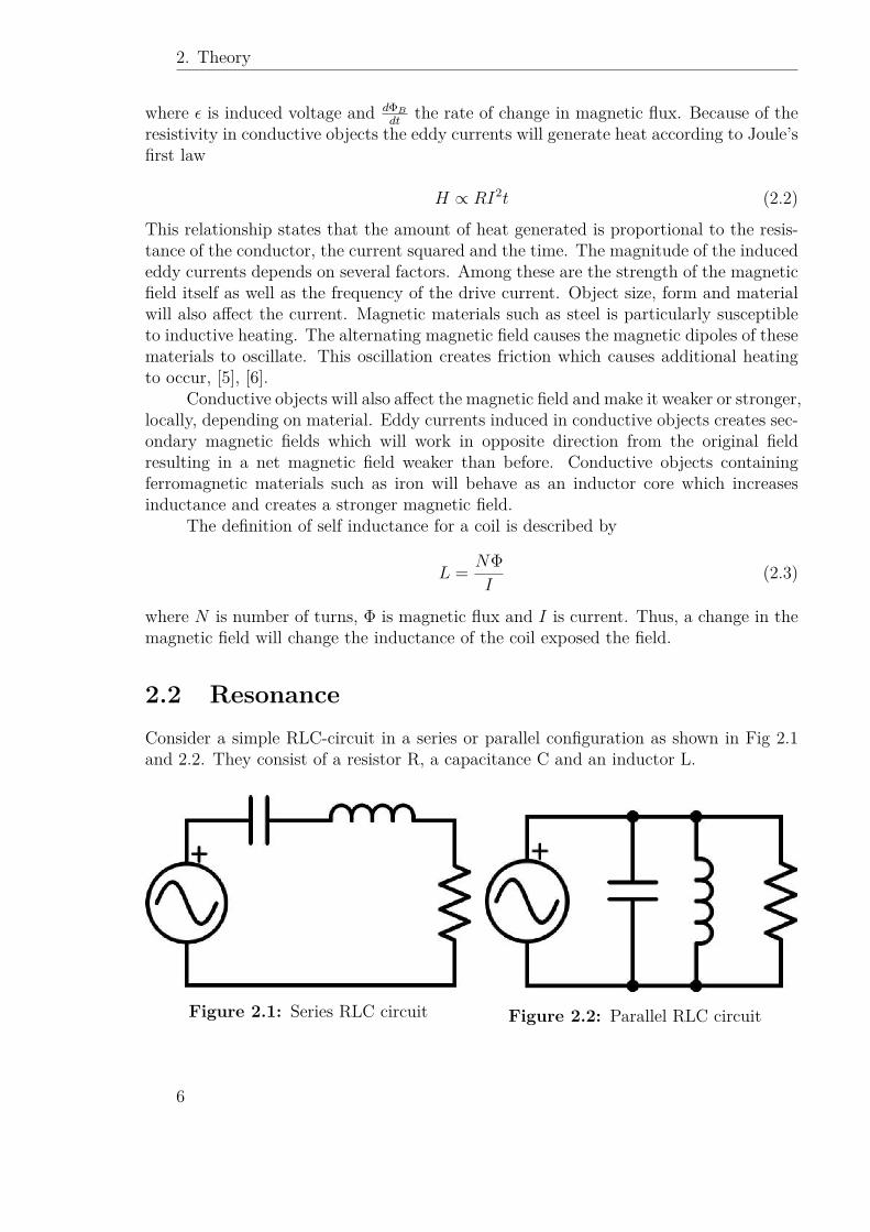
2.2 ResonanceConsider a simple RLC-circuit in a series or parallel configuration as shown in Fig 2.1and 2.2. They consist of a resistor R, a capacitance C and an inductor L.
Figure 2.1: Series RLC circuit Figure 2.2: Parallel RLC circuit
6
2. Theory
The impedance of these circuits are
ZS = ZR + ZC + ZL = R + 1jωC
+ jωL (2.4)
for the series circuit and1ZP
= 1ZR
+ 1ZC
+ 1ZL
= 1R
+ jωC + 1jωL
(2.5)
for the parallel circuit. Equation 2.4 and 2.5 can be rearranged as a real and an imaginarypart.
ZS = R + jω2LC − 1
ωC(2.6)
and
ZP = ω2C2R
1− 2ω2CL+ ω4C2L2 + ω2C2 + jωCR− ω3C2LR
1− 2ω2CL+ ω4C2L2 + ω2C2 (2.7)
At a certain frequency the imaginary parts in Eq. 2.6 and 2.7 becomes zero and forboth configurations this happens when ω = 1√
LC. This frequency is called the resonance
frequency and denoted ω0, and is related to the inductance and capacitance by
ω0 = 1√LC
(2.8)
When in resonance the LC part of the circuit acts as a short circuit for the se-ries configuration and as an open circuit for the parallel configuration. Therefore, theimpedance simplifies to
ZS = ZP = R (2.9)Ohm’s law described by Eq. 2.10 gives the relationship between the input voltage,
the system impedance, and the current.V = Z · I (2.10)
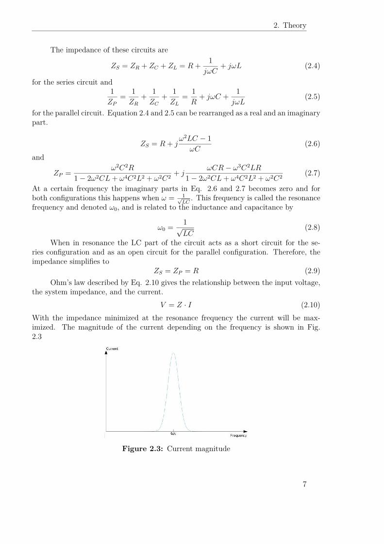
With the impedance minimized at the resonance frequency the current will be max-imized. The magnitude of the current depending on the frequency is shown in Fig.2.3
Figure 2.3: Current magnitude
7
2. Theory
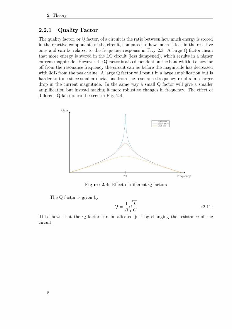
2.2.1 Quality FactorThe quality factor, or Q factor, of a circuit is the ratio between how much energy is storedin the reactive components of the circuit, compared to how much is lost in the resistiveones and can be related to the frequency response in Fig. 2.3. A large Q factor meanthat more energy is stored in the LC circuit (less dampened), which results in a highercurrent magnitude. However the Q factor is also dependent on the bandwidth, i.e how faroff from the resonance frequency the circuit can be before the magnitude has decreasedwith 3dB from the peak value. A large Q factor will result in a large amplification but isharder to tune since smaller deviations from the resonance frequency results in a largerdrop in the current magnitude. In the same way a small Q factor will give a smalleramplification but instead making it more robust to changes in frequency. The effect ofdifferent Q factors can be seen in Fig. 2.4.
Figure 2.4: Effect of different Q factors
The Q factor is given by
Q = 1R
√L
C(2.11)
This shows that the Q factor can be affected just by changing the resistance of thecircuit.
8
3Choice of Sensor Technologies
Several methods for detecting conductive objects and detecting live beings already existsfor many applications. Pros and cons of using these different methods in the limitedspace under a car will be evaluated in this chapter. According to the requirementspecification, live beings larger or equal in size to a hedgehog should be detected whileconductive objects the size of a coin and larger should be detected. It is desirable toavoid false positives. However, it is more important to eliminate false negatives. Forexample, there should under no circumstances be a large living being under the car whilethe charging is in progress. If the same sensor was to be used for detection of both livebeings and conductive objects, one would expect a large amount of false positives. Thisis because sensors that can detect both would be unable to distinguish between smallconductive objects and other kinds of small objects. Therefore a decision was made touse two different kinds of sensors, one for live beings and one for conductive objects.
3.1 Detection of Live BeingsThe following methods were considered to use for detection of live beings.
• Motion detectors (Passive infrared (PIR) and ultrasound)• IR heat sensor or cameras• Camera and image analysis• Ultrasonic distance sensors• Ultrasonic tripwires
Ultrasonic motion detectors work by sending out an ultrasonic pulse and thenmeasuring the frequency of the echo. The Doppler effect will cause the frequency of theresponse to increase if the detected object was moving towards the sensor, or decreaseif the object was moving away. PIR sensors work by measuring the amount of infraredradiation that is hitting the sensor. If this amount changes between one time instanceand the next, the sensor knows that an object has moved. A downside of motion detectorsis that they can not differentiate between an object leaving the area of detection andan object that has simply stopped moving. This means that motion sensors can not beused to detect the absence of live beings. Therefore, it cannot be used to automaticallyrestart the charging process when a live being has left the dangerous space.
IR heat sensors sense the temperature of objects by detecting how much infrared
9
3. Choice of Sensor Technologies
light they emit. Since the temperature of live beings usually differ from the ground’s,this could be used to detect them. One downside is that the sensor has to be placed closeto the ground, and asphalt can be rather hot in summer. This could make it difficult todetect live beings as the temperature gap between the live being and the ground mightnot be large enough that the sensor can differentiate between them. Another downsideis that a sufficiently thick shielding object can block the sensor.
Using a camera in combination with image analysis could also be blocked by ashielding object. Although, the camera would be able to detect a shielding object andsend a signal to stop the charging if that was the case. Furthermore, the camera lens issensitive to dirt and using a camera is the most complex and expensive method.
Ultrasonic distance sensors work by sending a directional burst of ultrasonic soundand then measuring the time until an echo returns. An advantage of using this sensor isthat it can be placed horizontally. This is because the distance measurement allows thesensor to distinguish between an object inside versus and object outside the dangerousarea. A downside is that the sensitivity is dependent on the surface properties of theobject. They work best with hard flat surfaces. Sound absorbent surfaces like fur givesreduced range and area of detection.
Ultrasonic tripwires are pairs of ultrasonic transmitters and receivers that sendpulses between them. If an object is between them, it will block and deflect the sound.The decrease in amplitude of the sound will then be detected by the receiver. Multiplereceivers can listen to the same transmitter to give better coverage. However, sufficientcoverage requires many sensors. A side effect of this is that the electronics neededincreases with every added sensor. Another downside shared by both ultrasonic tripwiresand distance sensors is that they will detect inanimate objects as well as live beings.
A decision was made to use a combination of ultrasonic distance sensors and trip-wires. This do not require a position on the underside of the car, nor do they requirespecial ground clearance, as cameras and heat sensors do. Having the sensors built-in tothe car rather than in the charging stations would require more of them. This is becausethere will be more cars than charging stations. It would also require adding wirelesscommunication to the system. Adding ground clearance for the sensors makes it likelythat they eventually will be damaged, by for example accidentally be hit by the car whenparking. The main reason to use them rather than motion detectors was that ultrasonicdistance sensors enables the system to know when the live being detected has left thedangerous area. In comparison, false alarms from inanimate objects, which is possiblewith ultrasonic distance sensors, is a smaller issue since the detection area will be undera car. It will also be possible to detect larger conductive objects making the conductiveobjects detection subsystem more reliable. Another advantage of using both distancesensors and tripwires is that the ultrasonic pulse from the distance sensors can be usedas the transmitter for the tripwires. A combination of these two systems will give anincreased sensor coverage and making it easier to detect sound absorbing materials likefur with the same number of sensors.
10
3. Choice of Sensor Technologies
3.2 Detection of Conductive ObjectsFor detection of conductive objects, two common techniques were considered
• Magnetometer• Inductive sensor
Magnetometers are used to measure the direction and strength of magnetic fields.Thus, it can be used to detect metals because of the changes in the magnetic field theycause. They are mostly used in applications with static magnetic fields such as Earth’smagnetic field. However, a few sensors can measure alternating fields up to a few kHz.With the charging field being approximately 90kHz this means that an external fieldwould have to be created using much lower frequency. However, the sensors are sensitiveto alternating fields other than the one it measures because it causes interference withthe detection and limits its effectiveness, [7], [8].
Inductive sensors are used in many modern metal detectors, e.g. treasure huntingand traffic light systems. These systems, also known as search coil sensors or inductionloop sensors consist of two coils, a transmitter and a receiver coil. The pair functionsmuch in the same way as a transformer. An ac voltage is applied to the transmittercoil which generates an alternating magnetic field. The receiver coil then acts as anantenna and current is induced in it. Both coils are also connected to an LC circuitusing the same resonance frequency. A reference point is first established with no con-ductive object nearby. When a conductive object is placed in close proximity it will,as previously mentioned, cause changes to the magnetic field and the inductance of thecoils. The change to the magnetic field will result in a change in the induced current.Furthermore, the change in inductance means that the system no longer operates at itsresonance frequency, which will decrease the induced current. The magnitude of dropwill depend on the Q factor. A larger Q factor will result in a bigger voltage drop. Theconductive object will also absorb some of the magnetic energy as heat, which will causean additional drop. Finally, there will be a phase shift in the induced current. Thephase shift occurs because of the phase response of the material. An inductive materialwhich conducts electricity easily is slow to react to changes in the current compared toa resistive material which does not conduct electricity easily.
Since the detection unit will be in close proximity to the charging field, using amagnetometer becomes problematic. A search coil sensor is deemed more reliable andwill be used in this project. It is not necessary to distinguish between different types ofconductive materials and it will thus not be necessary to study the phase shift. Instead,the amplitude of the induced voltage will be monitored to see if it differs from thereference value.
11

3. Choice of Sensor Technologies
12
4Design of Sensor Array
Ultrasonic distance sensors and ultrasonic receivers was purchased as finished compo-nents. The components are described in Chapter 5, only the placement of the sensorsare discussed in this chapter. The search coil sensors was designed from scratch sincesuitable complete search coils was not available for purchase.
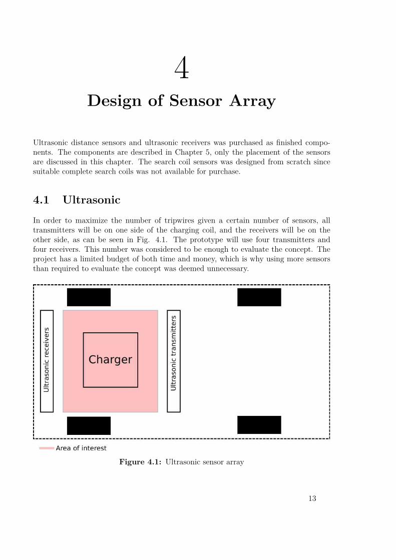
4.1 UltrasonicIn order to maximize the number of tripwires given a certain number of sensors, alltransmitters will be on one side of the charging coil, and the receivers will be on theother side, as can be seen in Fig. 4.1. The prototype will use four transmitters andfour receivers. This number was considered to be enough to evaluate the concept. Theproject has a limited budget of both time and money, which is why using more sensorsthan required to evaluate the concept was deemed unnecessary.
Figure 4.1: Ultrasonic sensor array
13
4. Design of Sensor Array
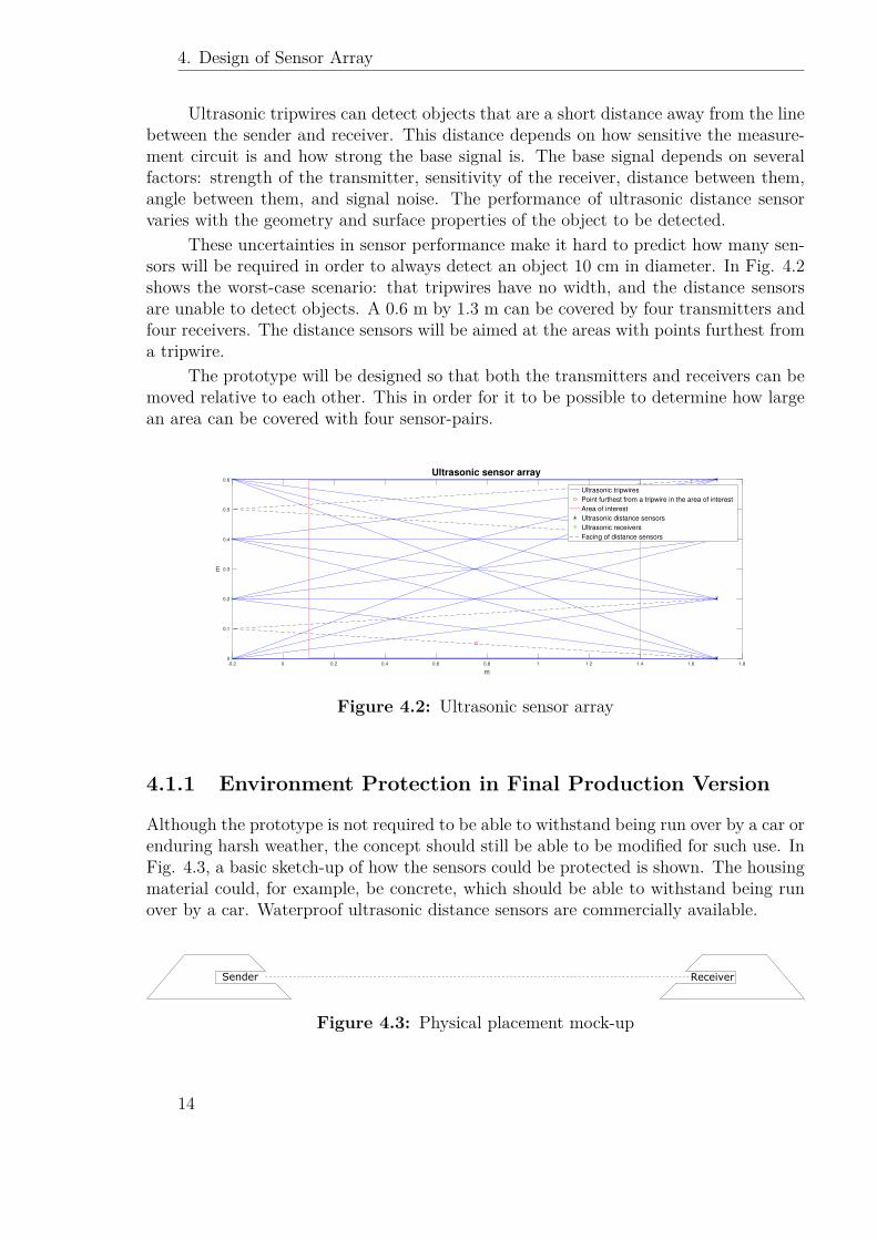
Ultrasonic tripwires can detect objects that are a short distance away from the linebetween the sender and receiver. This distance depends on how sensitive the measure-ment circuit is and how strong the base signal is. The base signal depends on severalfactors: strength of the transmitter, sensitivity of the receiver, distance between them,angle between them, and signal noise. The performance of ultrasonic distance sensorvaries with the geometry and surface properties of the object to be detected.
These uncertainties in sensor performance make it hard to predict how many sen-sors will be required in order to always detect an object 10 cm in diameter. In Fig. 4.2shows the worst-case scenario: that tripwires have no width, and the distance sensorsare unable to detect objects. A 0.6 m by 1.3 m can be covered by four transmitters andfour receivers. The distance sensors will be aimed at the areas with points furthest froma tripwire.
The prototype will be designed so that both the transmitters and receivers can bemoved relative to each other. This in order for it to be possible to determine how largean area can be covered with four sensor-pairs.
-0.2 0 0.2 0.4 0.6 0.8 1 1.2 1.4 1.6 1.8
m
0
0.1
0.2
0.3
0.4
0.5
0.6
m
Ultrasonic sensor array
Ultrasonic tripwires
Point furthest from a tripwire in the area of interest
Area of interest
Ultrasonic distance sensors
Ultrasonic receivers
Facing of distance sensors
Figure 4.2: Ultrasonic sensor array
4.1.1 Environment Protection in Final Production Version
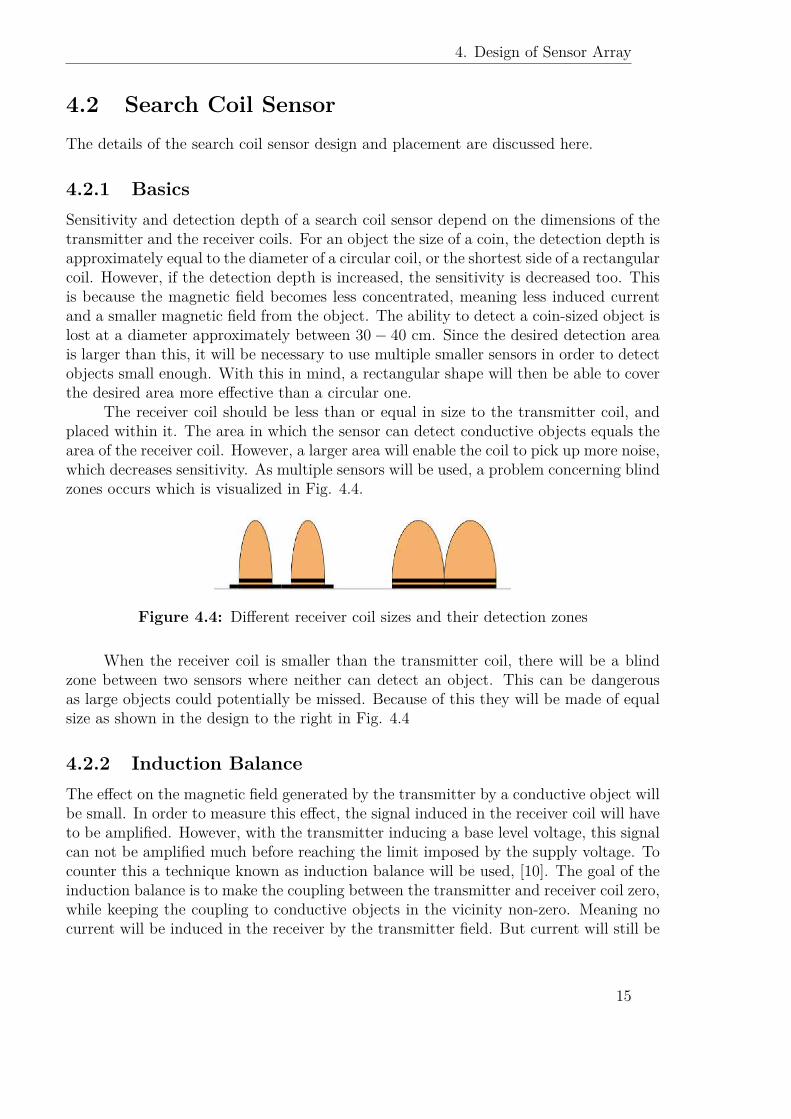
Although the prototype is not required to be able to withstand being run over by a car orenduring harsh weather, the concept should still be able to be modified for such use. InFig. 4.3, a basic sketch-up of how the sensors could be protected is shown. The housingmaterial could, for example, be concrete, which should be able to withstand being runover by a car. Waterproof ultrasonic distance sensors are commercially available.
Sender Receiver
Figure 4.3: Physical placement mock-up
14
4. Design of Sensor Array
4.2 Search Coil SensorThe details of the search coil sensor design and placement are discussed here.
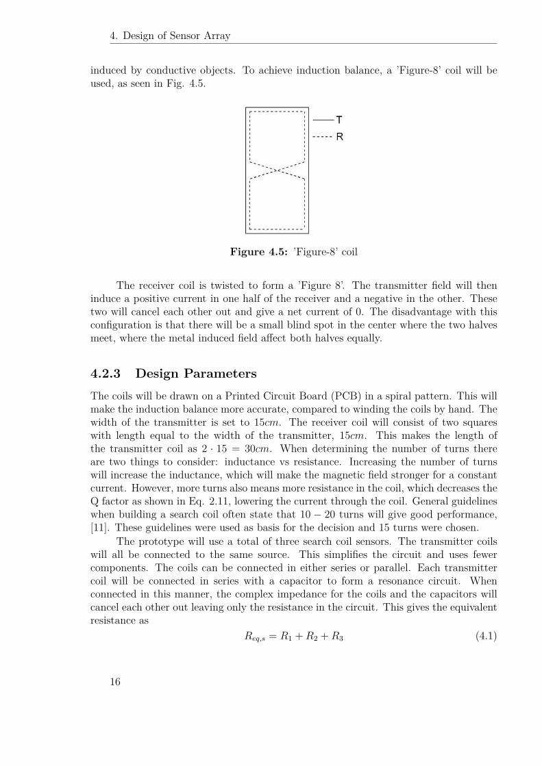
4.2.1 BasicsSensitivity and detection depth of a search coil sensor depend on the dimensions of thetransmitter and the receiver coils. For an object the size of a coin, the detection depth isapproximately equal to the diameter of a circular coil, or the shortest side of a rectangularcoil. However, if the detection depth is increased, the sensitivity is decreased too. Thisis because the magnetic field becomes less concentrated, meaning less induced currentand a smaller magnetic field from the object. The ability to detect a coin-sized object islost at a diameter approximately between 30− 40 cm. Since the desired detection areais larger than this, it will be necessary to use multiple smaller sensors in order to detectobjects small enough. With this in mind, a rectangular shape will then be able to coverthe desired area more effective than a circular one.
The receiver coil should be less than or equal in size to the transmitter coil, andplaced within it. The area in which the sensor can detect conductive objects equals thearea of the receiver coil. However, a larger area will enable the coil to pick up more noise,which decreases sensitivity. As multiple sensors will be used, a problem concerning blindzones occurs which is visualized in Fig. 4.4.
Figure 4.4: Different receiver coil sizes and their detection zones
When the receiver coil is smaller than the transmitter coil, there will be a blindzone between two sensors where neither can detect an object. This can be dangerousas large objects could potentially be missed. Because of this they will be made of equalsize as shown in the design to the right in Fig. 4.4
4.2.2 Induction BalanceThe effect on the magnetic field generated by the transmitter by a conductive object willbe small. In order to measure this effect, the signal induced in the receiver coil will haveto be amplified. However, with the transmitter inducing a base level voltage, this signalcan not be amplified much before reaching the limit imposed by the supply voltage. Tocounter this a technique known as induction balance will be used, [10]. The goal of theinduction balance is to make the coupling between the transmitter and receiver coil zero,while keeping the coupling to conductive objects in the vicinity non-zero. Meaning nocurrent will be induced in the receiver by the transmitter field. But current will still be
15
4. Design of Sensor Array
induced by conductive objects. To achieve induction balance, a ’Figure-8’ coil will beused, as seen in Fig. 4.5.
Figure 4.5: ’Figure-8’ coil
The receiver coil is twisted to form a ’Figure 8’. The transmitter field will theninduce a positive current in one half of the receiver and a negative in the other. Thesetwo will cancel each other out and give a net current of 0. The disadvantage with thisconfiguration is that there will be a small blind spot in the center where the two halvesmeet, where the metal induced field affect both halves equally.
4.2.3 Design ParametersThe coils will be drawn on a Printed Circuit Board (PCB) in a spiral pattern. This willmake the induction balance more accurate, compared to winding the coils by hand. Thewidth of the transmitter is set to 15cm. The receiver coil will consist of two squareswith length equal to the width of the transmitter, 15cm. This makes the length ofthe transmitter coil as 2 · 15 = 30cm. When determining the number of turns thereare two things to consider: inductance vs resistance. Increasing the number of turnswill increase the inductance, which will make the magnetic field stronger for a constantcurrent. However, more turns also means more resistance in the coil, which decreases theQ factor as shown in Eq. 2.11, lowering the current through the coil. General guidelineswhen building a search coil often state that 10 − 20 turns will give good performance,[11]. These guidelines were used as basis for the decision and 15 turns were chosen.
The prototype will use a total of three search coil sensors. The transmitter coilswill all be connected to the same source. This simplifies the circuit and uses fewercomponents. The coils can be connected in either series or parallel. Each transmittercoil will be connected in series with a capacitor to form a resonance circuit. Whenconnected in this manner, the complex impedance for the coils and the capacitors willcancel each other out leaving only the resistance in the circuit. This gives the equivalentresistance as
Req,s = R1 +R2 +R3 (4.1)
16
4. Design of Sensor Array
for a series configuration and1
Req,p
= 1R1
+ 1R1
+ 1R1→ Req,p = R1R2R3
R1R2 +R1R3 +R2R3(4.2)
for a parallel configuration, with index 1, 2, and 3 corresponding to coil 1, 2, and 3. Thecoils will be identical in size and shape and thus R1 = R2 = R3 = R, and Eq. 4.1, and4.2 simplifies to
Req,s = 3R (4.3)and
Req,p = R
3 (4.4)
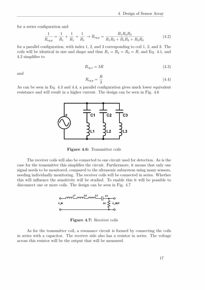
As can be seen in Eq. 4.3 and 4.4, a parallel configuration gives much lower equivalentresistance and will result in a higher current. The design can be seen in Fig. 4.6
Figure 4.6: Transmitter coils
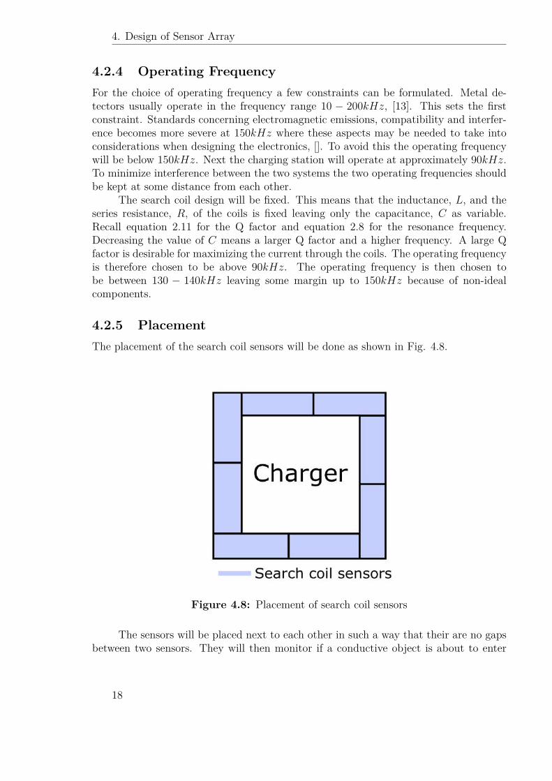
The receiver coils will also be connected to one circuit used for detection. As is thecase for the transmitter this simplifies the circuit. Furthermore, it means that only onesignal needs to be monitored, compared to the ultrasonic subsystem using many sensors,needing individually monitoring. The receiver coils will be connected in series. Whetherthis will influence the sensitivity will be studied. To enable this it will be possible todisconnect one or more coils. The design can be seen in Fig. 4.7
Figure 4.7: Receiver coils
As for the transmitter coil, a resonance circuit is formed by connecting the coilsin series with a capacitor. The receiver side also has a resistor in series. The voltageacross this resistor will be the output that will be measured.
17
4. Design of Sensor Array
4.2.4 Operating FrequencyFor the choice of operating frequency a few constraints can be formulated. Metal de-tectors usually operate in the frequency range 10 − 200kHz, [13]. This sets the firstconstraint. Standards concerning electromagnetic emissions, compatibility and interfer-ence becomes more severe at 150kHz where these aspects may be needed to take intoconsiderations when designing the electronics, []. To avoid this the operating frequencywill be below 150kHz. Next the charging station will operate at approximately 90kHz.To minimize interference between the two systems the two operating frequencies shouldbe kept at some distance from each other.
The search coil design will be fixed. This means that the inductance, L, and theseries resistance, R, of the coils is fixed leaving only the capacitance, C as variable.Recall equation 2.11 for the Q factor and equation 2.8 for the resonance frequency.Decreasing the value of C means a larger Q factor and a higher frequency. A large Qfactor is desirable for maximizing the current through the coils. The operating frequencyis therefore chosen to be above 90kHz. The operating frequency is then chosen tobe between 130 − 140kHz leaving some margin up to 150kHz because of non-idealcomponents.
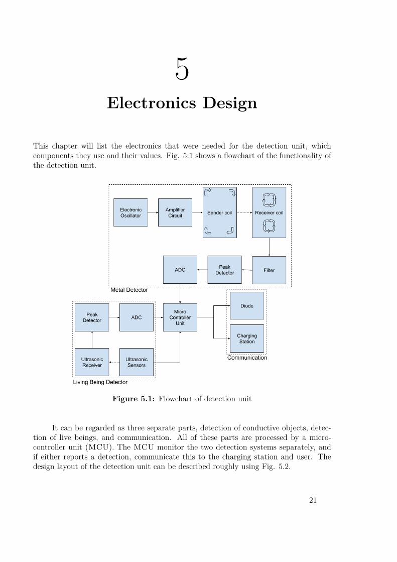
4.2.5 PlacementThe placement of the search coil sensors will be done as shown in Fig. 4.8.
Charger
Figure 4.8: Placement of search coil sensors
The sensors will be placed next to each other in such a way that their are no gapsbetween two sensors. They will then monitor if a conductive object is about to enter
18

4. Design of Sensor Array
the charging area.
4.2.6 Input and OutputBoth the input and the output to the search coil sensor will be an ac voltage. The inputis applied to the transmitter coil and the output is obtained at the receiver coil.
19

4. Design of Sensor Array
20
5Electronics Design
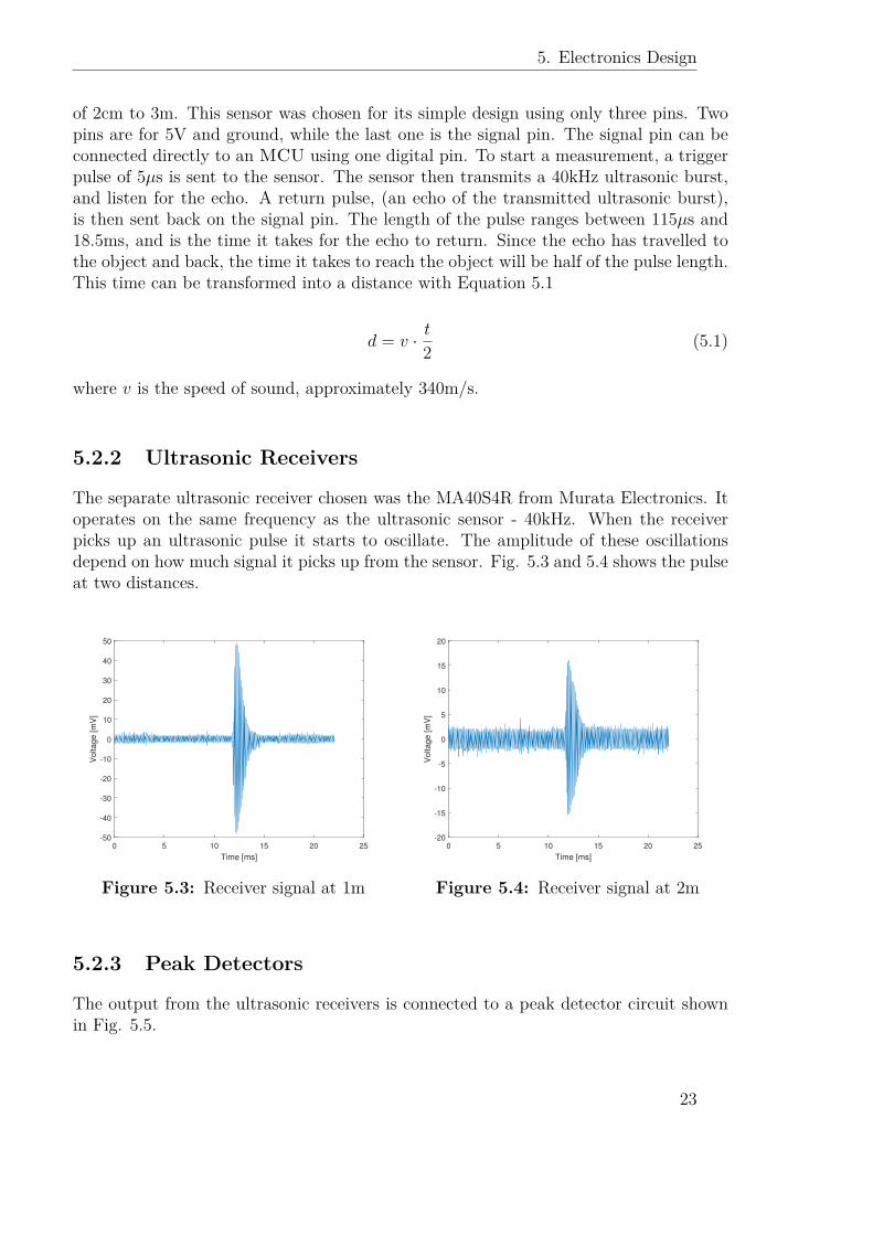
This chapter will list the electronics that were needed for the detection unit, whichcomponents they use and their values. Fig. 5.1 shows a flowchart of the functionality ofthe detection unit.
Figure 5.1: Flowchart of detection unit
It can be regarded as three separate parts, detection of conductive objects, detec-tion of live beings, and communication. All of these parts are processed by a micro-controller unit (MCU). The MCU monitor the two detection systems separately, andif either reports a detection, communicate this to the charging station and user. Thedesign layout of the detection unit can be described roughly using Fig. 5.2.
21

5. Electronics Design
Figure 5.2: Detection unit layout
The search coil sensors are placed around the charging unit. They are connectedto a printed circuit board (PCB) containing all subparts for the conductive objectdetection, as well as the MCU. The ultrasonic sensors are connected directly to theMCU using one of its digital pins each. They are also disconnected from the rest of theelectronics, to allowing change of positions. Each ultrasonic receiver is placed on a PCBof their own. Each PCB contains their own separate set of the subblock Peak Detector.The receivers are placed close to an external Analog-to-Digital Converter (ADC) inorder to minimize the length of the analog signal lines. Finally, the ADC is connectedto the MCU using digital pins.
5.1 Power SupplyInput to the PCB will be a 12V dc voltage supplied from an external power supply.Some components, like the MCU, require 5V. Thus a voltage regulator was needed. Forthis, an LM7805 linear voltage regulator from Fairchild was chosen. It uses three pins,input voltage, ground, and output voltage. The input voltage has a maximum limit of35V. The output voltage is fixed at 5V, and can deliver up to 1A of continuous outputcurrent.
5.2 Detection of Live BeingsThis section lists the electronics that was used for the live being detection system.
5.2.1 Ultrasonic SensorsFor the ultrasonic sensors, the PING))) Ultrasonic Distance Sensor from PARALLAXwas chosen. Equipped with both a transmitter and a receiver, it has a detection range
22
5. Electronics Design
of 2cm to 3m. This sensor was chosen for its simple design using only three pins. Twopins are for 5V and ground, while the last one is the signal pin. The signal pin can beconnected directly to an MCU using one digital pin. To start a measurement, a triggerpulse of 5µs is sent to the sensor. The sensor then transmits a 40kHz ultrasonic burst,and listen for the echo. A return pulse, (an echo of the transmitted ultrasonic burst),is then sent back on the signal pin. The length of the pulse ranges between 115µs and18.5ms, and is the time it takes for the echo to return. Since the echo has travelled tothe object and back, the time it takes to reach the object will be half of the pulse length.This time can be transformed into a distance with Equation 5.1
d = v · t2 (5.1)
where v is the speed of sound, approximately 340m/s.
5.2.2 Ultrasonic Receivers
The separate ultrasonic receiver chosen was the MA40S4R from Murata Electronics. Itoperates on the same frequency as the ultrasonic sensor - 40kHz. When the receiverpicks up an ultrasonic pulse it starts to oscillate. The amplitude of these oscillationsdepend on how much signal it picks up from the sensor. Fig. 5.3 and 5.4 shows the pulseat two distances.
0 5 10 15 20 25
Time [ms]
-50
-40
-30
-20
-10
0
10
20
30
40
50
Voltage [m
V]
Figure 5.3: Receiver signal at 1m
0 5 10 15 20 25
Time [ms]
-20
-15
-10
-5
0
5
10
15
20
Voltage [m
V]
Figure 5.4: Receiver signal at 2m
5.2.3 Peak Detectors
The output from the ultrasonic receivers is connected to a peak detector circuit shownin Fig. 5.5.
23
5. Electronics Design
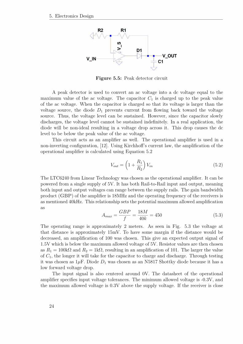
Figure 5.5: Peak detector circuit
A peak detector is used to convert an ac voltage into a dc voltage equal to themaximum value of the ac voltage. The capacitor C1 is charged up to the peak valueof the ac voltage. When the capacitor is charged so that its voltage is larger than thevoltage source, the diode D1 prevents current from flowing back toward the voltagesource. Thus, the voltage level can be sustained. However, since the capacitor slowlydischarges, the voltage level cannot be sustained indefinitely. In a real application, thediode will be non-ideal resulting in a voltage drop across it. This drop causes the dclevel to be below the peak value of the ac voltage.
This circuit acts as an amplifier as well. The operational amplifier is used in anon-inverting configuration, [12]. Using Kirchhoff’s current law, the amplification of theoperational amplifier is calculated using Equation 5.2
Vout =(
1 + R1
R2
)Vin (5.2)
The LTC6240 from Linear Technology was chosen as the operational amplifier. It can bepowered from a single supply of 5V. It has both Rail-to-Rail input and output, meaningboth input and output voltages can range between the supply rails. The gain bandwidthproduct (GBP) of the amplifier is 18MHz and the operating frequency of the receivers isas mentioned 40kHz. This relationship sets the potential maximum allowed amplificationas
Amax = GBP
f= 18M
40k = 450 (5.3)
The operating range is approximately 2 meters. As seen in Fig. 5.3 the voltage atthat distance is approximately 15mV. To have some margin if the distance would bedecreased, an amplification of 100 was chosen. This give an expected output signal of1.5V which is below the maximum allowed voltage of 5V. Resistor values are then chosenas R1 = 100kΩ and R2 = 1kΩ, resulting in an amplification of 101. The larger the valueof C1, the longer it will take for the capacitor to charge and discharge. Through testingit was chosen as 1µF. Diode D1 was chosen as an N5817 Shottky diode because it has alow forward voltage drop.
The input signal is also centered around 0V. The datasheet of the operationalamplifier specifies input voltage tolerances. The minimum allowed voltage is -0.3V, andthe maximum allowed voltage is 0.3V above the supply voltage. If the receiver is close
24
5. Electronics Design
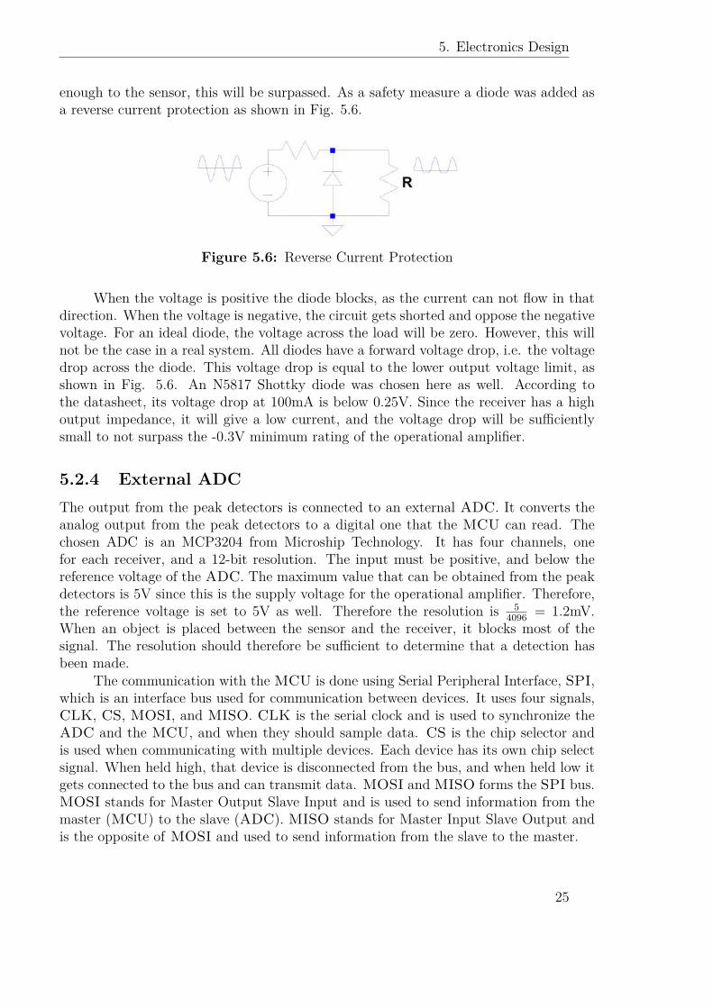
enough to the sensor, this will be surpassed. As a safety measure a diode was added asa reverse current protection as shown in Fig. 5.6.
Figure 5.6: Reverse Current Protection
When the voltage is positive the diode blocks, as the current can not flow in thatdirection. When the voltage is negative, the circuit gets shorted and oppose the negativevoltage. For an ideal diode, the voltage across the load will be zero. However, this willnot be the case in a real system. All diodes have a forward voltage drop, i.e. the voltagedrop across the diode. This voltage drop is equal to the lower output voltage limit, asshown in Fig. 5.6. An N5817 Shottky diode was chosen here as well. According tothe datasheet, its voltage drop at 100mA is below 0.25V. Since the receiver has a highoutput impedance, it will give a low current, and the voltage drop will be sufficientlysmall to not surpass the -0.3V minimum rating of the operational amplifier.
5.2.4 External ADCThe output from the peak detectors is connected to an external ADC. It converts theanalog output from the peak detectors to a digital one that the MCU can read. Thechosen ADC is an MCP3204 from Microship Technology. It has four channels, onefor each receiver, and a 12-bit resolution. The input must be positive, and below thereference voltage of the ADC. The maximum value that can be obtained from the peakdetectors is 5V since this is the supply voltage for the operational amplifier. Therefore,the reference voltage is set to 5V as well. Therefore the resolution is 5
4096 = 1.2mV.When an object is placed between the sensor and the receiver, it blocks most of thesignal. The resolution should therefore be sufficient to determine that a detection hasbeen made.
The communication with the MCU is done using Serial Peripheral Interface, SPI,which is an interface bus used for communication between devices. It uses four signals,CLK, CS, MOSI, and MISO. CLK is the serial clock and is used to synchronize theADC and the MCU, and when they should sample data. CS is the chip selector andis used when communicating with multiple devices. Each device has its own chip selectsignal. When held high, that device is disconnected from the bus, and when held low itgets connected to the bus and can transmit data. MOSI and MISO forms the SPI bus.MOSI stands for Master Output Slave Input and is used to send information from themaster (MCU) to the slave (ADC). MISO stands for Master Input Slave Output andis the opposite of MOSI and used to send information from the slave to the master.
25
5. Electronics Design
5.3 Detection of Conductive ObjectsThe conductive objects detection system consists of two subsystems, sender and receiver.
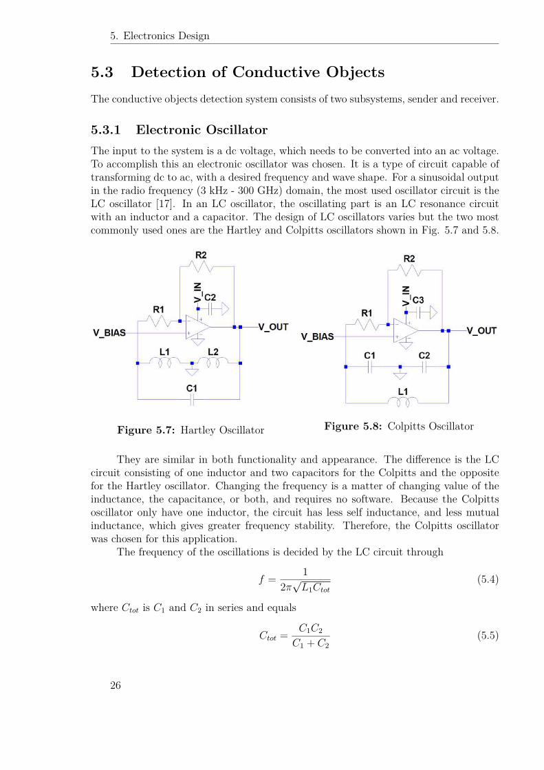
5.3.1 Electronic OscillatorThe input to the system is a dc voltage, which needs to be converted into an ac voltage.To accomplish this an electronic oscillator was chosen. It is a type of circuit capable oftransforming dc to ac, with a desired frequency and wave shape. For a sinusoidal outputin the radio frequency (3 kHz - 300 GHz) domain, the most used oscillator circuit is theLC oscillator [17]. In an LC oscillator, the oscillating part is an LC resonance circuitwith an inductor and a capacitor. The design of LC oscillators varies but the two mostcommonly used ones are the Hartley and Colpitts oscillators shown in Fig. 5.7 and 5.8.
Figure 5.7: Hartley Oscillator Figure 5.8: Colpitts Oscillator
They are similar in both functionality and appearance. The difference is the LCcircuit consisting of one inductor and two capacitors for the Colpitts and the oppositefor the Hartley oscillator. Changing the frequency is a matter of changing value of theinductance, the capacitance, or both, and requires no software. Because the Colpittsoscillator only have one inductor, the circuit has less self inductance, and less mutualinductance, which gives greater frequency stability. Therefore, the Colpitts oscillatorwas chosen for this application.
The frequency of the oscillations is decided by the LC circuit through
f = 12π√L1Ctot
(5.4)
where Ctot is C1 and C2 in series and equals
Ctot = C1C2
C1 + C2(5.5)
26
5. Electronics Design
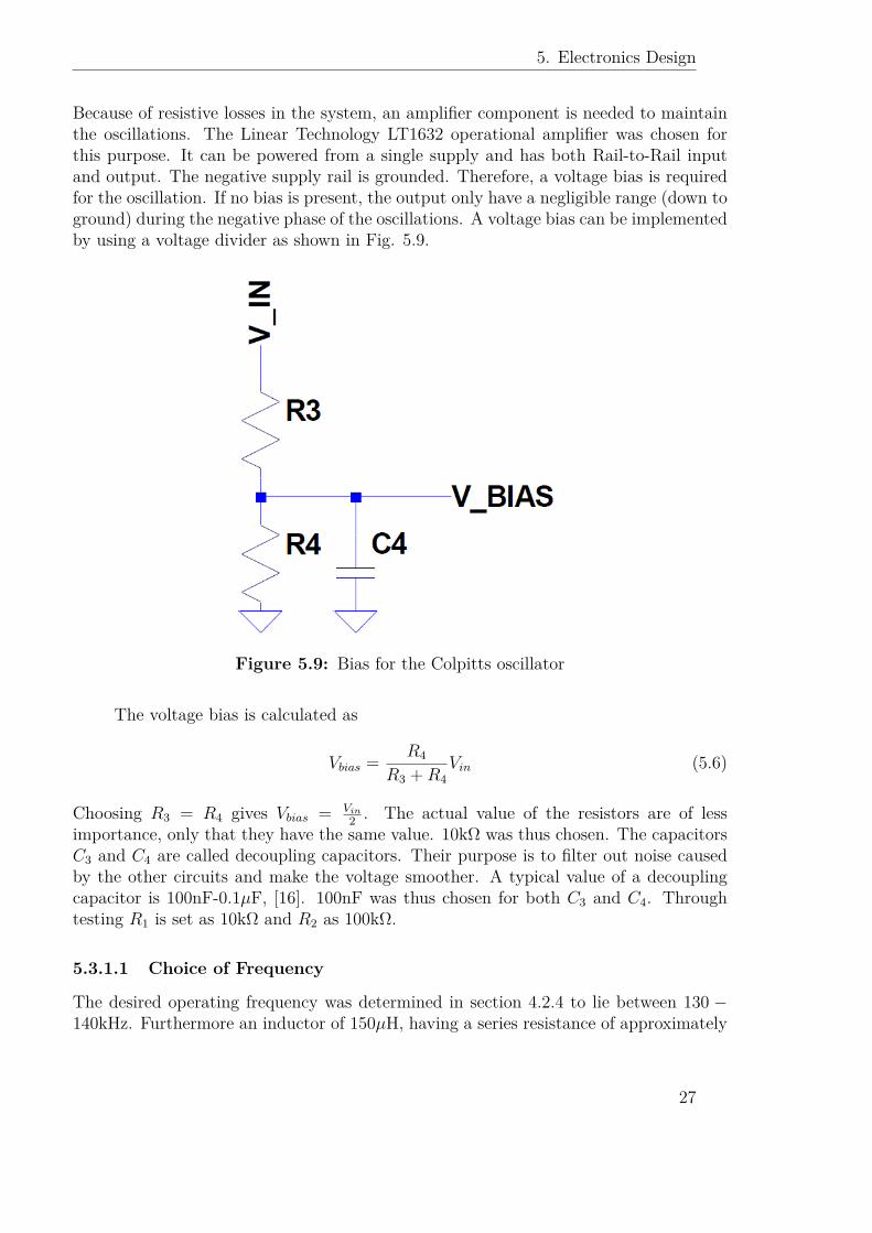
Because of resistive losses in the system, an amplifier component is needed to maintainthe oscillations. The Linear Technology LT1632 operational amplifier was chosen forthis purpose. It can be powered from a single supply and has both Rail-to-Rail inputand output. The negative supply rail is grounded. Therefore, a voltage bias is requiredfor the oscillation. If no bias is present, the output only have a negligible range (down toground) during the negative phase of the oscillations. A voltage bias can be implementedby using a voltage divider as shown in Fig. 5.9.
Figure 5.9: Bias for the Colpitts oscillator
The voltage bias is calculated as
Vbias = R4
R3 +R4Vin (5.6)
Choosing R3 = R4 gives Vbias = Vin
2 . The actual value of the resistors are of lessimportance, only that they have the same value. 10kΩ was thus chosen. The capacitorsC3 and C4 are called decoupling capacitors. Their purpose is to filter out noise causedby the other circuits and make the voltage smoother. A typical value of a decouplingcapacitor is 100nF-0.1µF, [16]. 100nF was thus chosen for both C3 and C4. Throughtesting R1 is set as 10kΩ and R2 as 100kΩ.
5.3.1.1 Choice of Frequency
The desired operating frequency was determined in section 4.2.4 to lie between 130 −140kHz. Furthermore an inductor of 150µH, having a series resistance of approximately
27

5. Electronics Design
10Ω, was chosen for the LC-circuit. The necessary capacitance, for a frequency of135kHz, can then be calculated as
Ctot = 14π2f 2L
= 14π21350002150µ = 9.27nF
Then if choosing C2 as 100nF the value of C1 can be calculated as
C1 = CtotC2
Ctot − C2= 9.27n100n
9.27n− 100n = 10.2nF
Closest value is then 10nF.
5.3.1.2 Simulation
The simulations in this section was performed using LTspice.
Figure 5.10: Simulation of output fromColpitts oscillator with an ideal induc-tance
Figure 5.11: Simulation of outputfrom Colpitts oscillator with an non-idealinductance(10Ω series resistance).
Simulation of the oscillator yields the graphs above. Fig. 5.10 shows the outputfrom the oscillator without series resistance in the inductor, and Fig. 5.11 shows theoutput from the oscillator with series resistance in the inductor. As can be seen the seriesresistance cause a decrease in amplitude from 10V peak-to-peak, with a max value of11V, to 1.5V peak-to-peak with a max value of 7.5V. There are also some distortionsto the voltage. The distortions will be ignored because they are relatively small. Theamplitude of the oscillator will be increased by the use of an amplifier circuit as seen inFig. 5.12.
28
5. Electronics Design
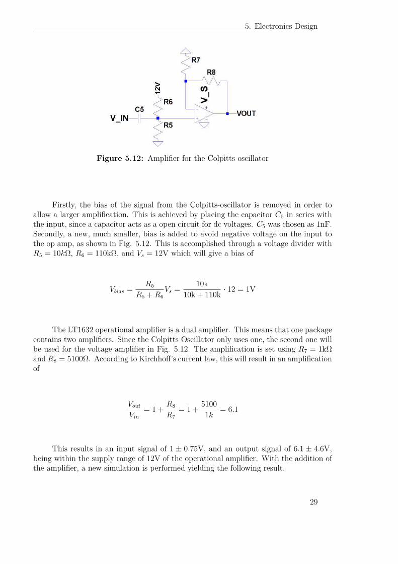
Figure 5.12: Amplifier for the Colpitts oscillator
Firstly, the bias of the signal from the Colpitts-oscillator is removed in order toallow a larger amplification. This is achieved by placing the capacitor C5 in series withthe input, since a capacitor acts as a open circuit for dc voltages. C5 was chosen as 1nF.Secondly, a new, much smaller, bias is added to avoid negative voltage on the input tothe op amp, as shown in Fig. 5.12. This is accomplished through a voltage divider withR5 = 10kΩ, R6 = 110kΩ, and Vs = 12V which will give a bias of
Vbias = R5
R5 +R6Vs = 10k
10k + 110k · 12 = 1V
The LT1632 operational amplifier is a dual amplifier. This means that one packagecontains two amplifiers. Since the Colpitts Oscillator only uses one, the second one willbe used for the voltage amplifier in Fig. 5.12. The amplification is set using R7 = 1kΩandR8 = 5100Ω. According to Kirchhoff’s current law, this will result in an amplificationof
Vout
Vin
= 1 + R8
R7= 1 + 5100
1k = 6.1
This results in an input signal of 1 ± 0.75V, and an output signal of 6.1 ± 4.6V,being within the supply range of 12V of the operational amplifier. With the addition ofthe amplifier, a new simulation is performed yielding the following result.
29
5. Electronics Design
Figure 5.13: Colpitts Oscillator with am-plifier
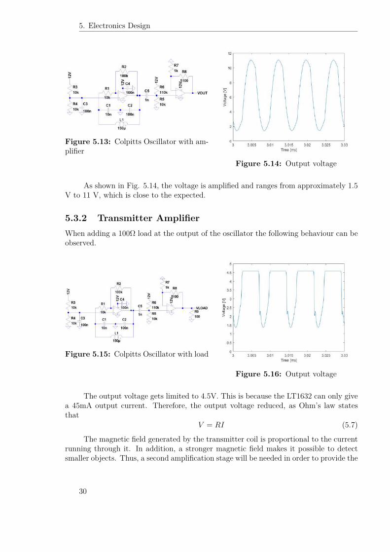
Figure 5.14: Output voltage
As shown in Fig. 5.14, the voltage is amplified and ranges from approximately 1.5V to 11 V, which is close to the expected.
5.3.2 Transmitter AmplifierWhen adding a 100Ω load at the output of the oscillator the following behaviour can beobserved.
Figure 5.15: Colpitts Oscillator with load
Figure 5.16: Output voltage
The output voltage gets limited to 4.5V. This is because the LT1632 can only givea 45mA output current. Therefore, the output voltage reduced, as Ohm’s law statesthat
V = RI (5.7)
The magnetic field generated by the transmitter coil is proportional to the currentrunning through it. In addition, a stronger magnetic field makes it possible to detectsmaller objects. Thus, a second amplification stage will be needed in order to provide the
30
5. Electronics Design
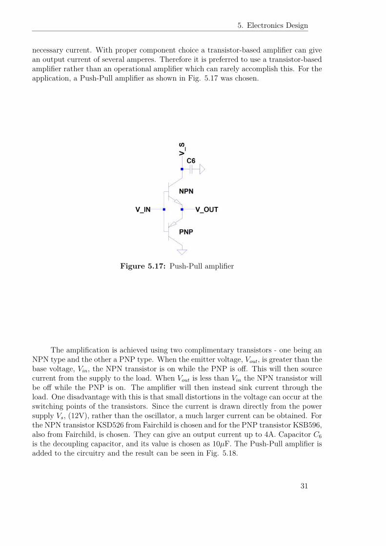
necessary current. With proper component choice a transistor-based amplifier can givean output current of several amperes. Therefore it is preferred to use a transistor-basedamplifier rather than an operational amplifier which can rarely accomplish this. For theapplication, a Push-Pull amplifier as shown in Fig. 5.17 was chosen.
Figure 5.17: Push-Pull amplifier
The amplification is achieved using two complimentary transistors - one being anNPN type and the other a PNP type. When the emitter voltage, Vout, is greater than thebase voltage, Vin, the NPN transistor is on while the PNP is off. This will then sourcecurrent from the supply to the load. When Vout is less than Vin the NPN transistor willbe off while the PNP is on. The amplifier will then instead sink current through theload. One disadvantage with this is that small distortions in the voltage can occur at theswitching points of the transistors. Since the current is drawn directly from the powersupply Vs, (12V), rather than the oscillator, a much larger current can be obtained. Forthe NPN transistor KSD526 from Fairchild is chosen and for the PNP transistor KSB596,also from Fairchild, is chosen. They can give an output current up to 4A. Capacitor C6is the decoupling capacitor, and its value is chosen as 10µF. The Push-Pull amplifier isadded to the circuitry and the result can be seen in Fig. 5.18.
31
5. Electronics Design
3 3.005 3.01 3.015 3.02 3.025 3.03
Time [ms]
0
2
4
6
8
10
12
Voltage [V
]
Figure 5.18: Push-Pull output with load
With the added circuitry, the voltage can be sustained at the desired voltage level,and the subsequent current is higher.
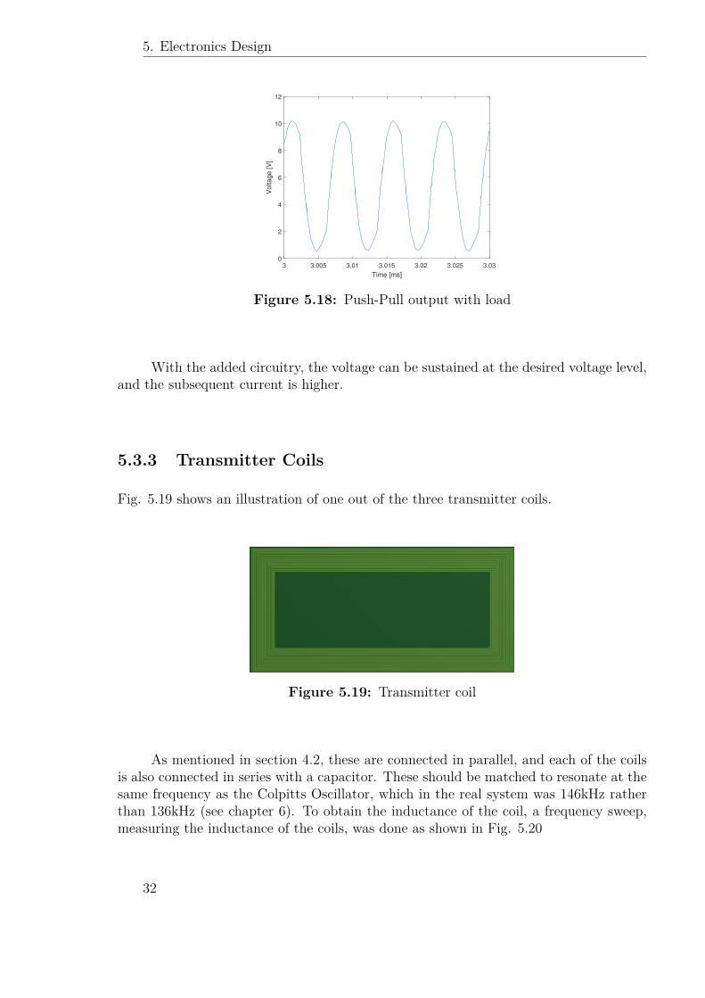
5.3.3 Transmitter Coils
Fig. 5.19 shows an illustration of one out of the three transmitter coils.
Figure 5.19: Transmitter coil
As mentioned in section 4.2, these are connected in parallel, and each of the coilsis also connected in series with a capacitor. These should be matched to resonate at thesame frequency as the Colpitts Oscillator, which in the real system was 146kHz ratherthan 136kHz (see chapter 6). To obtain the inductance of the coil, a frequency sweep,measuring the inductance of the coils, was done as shown in Fig. 5.20
32
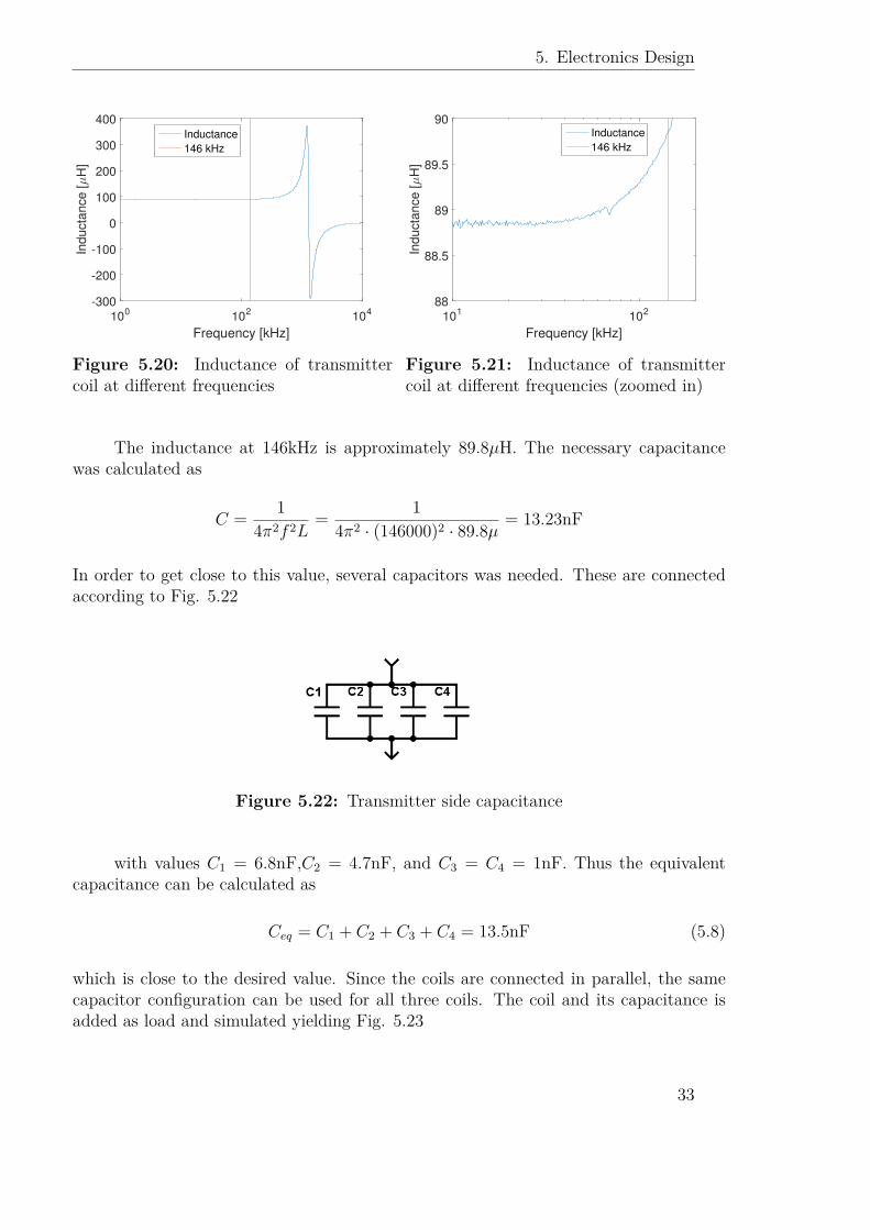
5. Electronics Design
100
102
104
Frequency [kHz]
-300
-200
-100
0
100
200
300
400
Ind
ucta
nce
[µ
H]
Inductance
146 kHz
Figure 5.20: Inductance of transmittercoil at different frequencies
101
102
Frequency [kHz]
88
88.5
89
89.5
90
Ind
ucta
nce
[µ
H]
Inductance
146 kHz
Figure 5.21: Inductance of transmittercoil at different frequencies (zoomed in)
The inductance at 146kHz is approximately 89.8µH. The necessary capacitancewas calculated as
C = 14π2f 2L
= 14π2 · (146000)2 · 89.8µ = 13.23nF
In order to get close to this value, several capacitors was needed. These are connectedaccording to Fig. 5.22
Figure 5.22: Transmitter side capacitance
with values C1 = 6.8nF,C2 = 4.7nF, and C3 = C4 = 1nF. Thus the equivalentcapacitance can be calculated as
Ceq = C1 + C2 + C3 + C4 = 13.5nF (5.8)
which is close to the desired value. Since the coils are connected in parallel, the samecapacitor configuration can be used for all three coils. The coil and its capacitance isadded as load and simulated yielding Fig. 5.23
33
5. Electronics Design
3 3.01 3.02 3.03
Time [ms]
-1
-0.5
0
0.5
1
Cu
rre
nt
[A]
Figure 5.23: Simulation of current through one coil
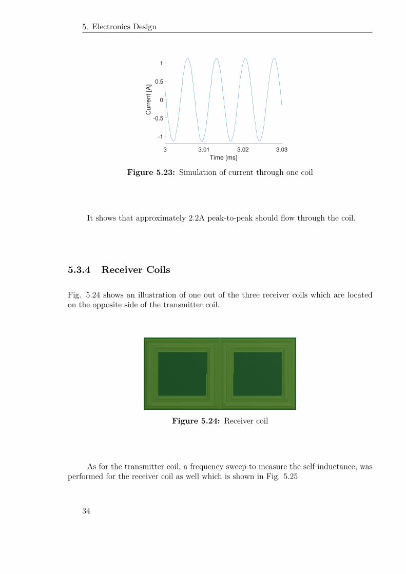
It shows that approximately 2.2A peak-to-peak should flow through the coil.
5.3.4 Receiver Coils
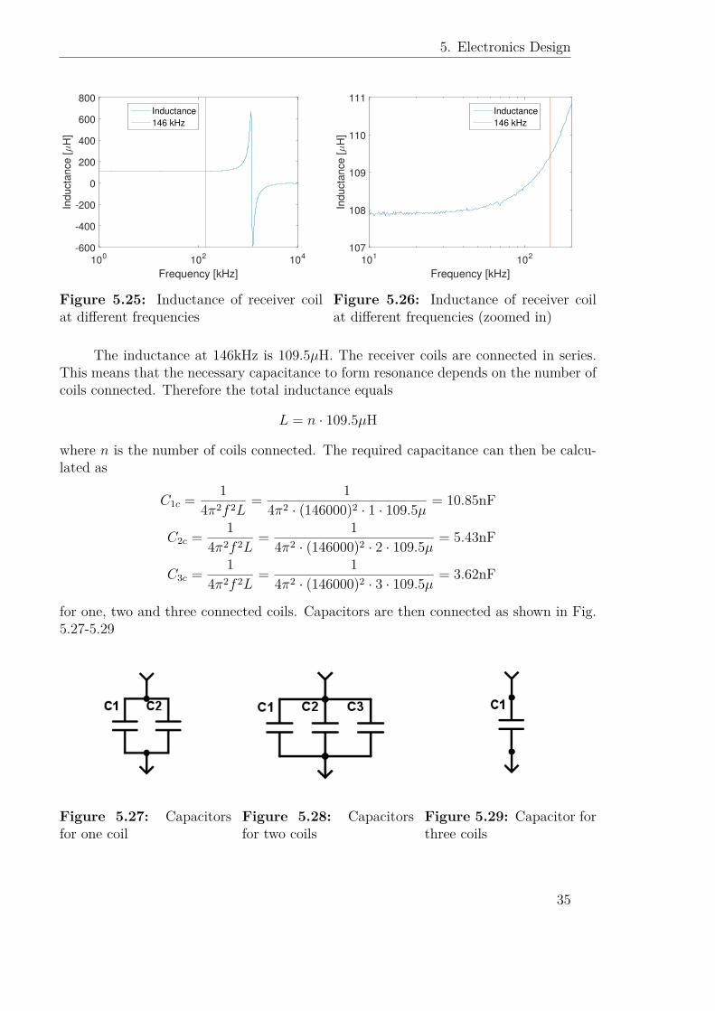
Fig. 5.24 shows an illustration of one out of the three receiver coils which are locatedon the opposite side of the transmitter coil.
Figure 5.24: Receiver coil
As for the transmitter coil, a frequency sweep to measure the self inductance, wasperformed for the receiver coil as well which is shown in Fig. 5.25
34
5. Electronics Design
100
102
104
Frequency [kHz]
-600
-400
-200
0
200
400
600
800
Ind
ucta
nce
[µ
H]
Inductance
146 kHz
Figure 5.25: Inductance of receiver coilat different frequencies
101
102
Frequency [kHz]
107
108
109
110
111
Ind
ucta
nce
[µ
H]
Inductance
146 kHz
Figure 5.26: Inductance of receiver coilat different frequencies (zoomed in)
The inductance at 146kHz is 109.5µH. The receiver coils are connected in series.This means that the necessary capacitance to form resonance depends on the number ofcoils connected. Therefore the total inductance equals
L = n · 109.5µH
where n is the number of coils connected. The required capacitance can then be calcu-lated as
C1c = 14π2f 2L
= 14π2 · (146000)2 · 1 · 109.5µ = 10.85nF
C2c = 14π2f 2L
= 14π2 · (146000)2 · 2 · 109.5µ = 5.43nF
C3c = 14π2f 2L
= 14π2 · (146000)2 · 3 · 109.5µ = 3.62nF
for one, two and three connected coils. Capacitors are then connected as shown in Fig.5.27-5.29
Figure 5.27: Capacitorsfor one coil
Figure 5.28: Capacitorsfor two coils
Figure 5.29: Capacitor forthree coils
35
5. Electronics Design
with C1 = 10nF, and C2 = 1nF for one coil, C1 = 3.3nF, C2 = C3 = 1nF for twocoils and C1 = 3.3nF for three coils.
The resistor the voltage will be measured across was chosen as 1Ω to give smalleffect on the Q factor.
5.3.5 FilterThe purpose of the search coil system is to operate in close proximity to the chargingstation. Therefore, the magnetic field from the charger can interfere with the detection,and create distortions in the signal. A band-stop filter centered around the frequencyof the charging station can filter out this interference while the search coil operatingfrequency remains unaffected. The frequency of the search coil system, 146kHz, is stillfairly close to the frequency of the charging station - 90kHz. Therefore, a filter with ahigh Q factor is needed in order to attenuate the 90kHz signal enough while leaving the146kHz signal intact. These types of filters are called notch filters, and in Fig. 5.30 onepossible implementation is shown.
Figure 5.30: Notch Filter Schematic
The circuit is a tunable notch filter and presented in the datasheet of the LinearTechnology LT1632 operational amplifier as a typical application. The component valueswere taken from the proposed circuit in the datasheet with the exception of R andR15. Also C12 were added as a decoupling capacitor and C13 and R21 for bias removal.Component values from the datasheet were
Table 5.1: Notch filter component values
C C7 C8 C9 R10 R11 R12 R13 R14 R16 R17 R181nF 2.2µF 4.7µF 4.7µF 500Ω 1kΩ 1kΩ 1kΩ 1kΩ 1kΩ 10kΩ 10kΩ
The notch frequency is calculated as
fnotch = 12πRC (5.9)
36
5. Electronics Design
By rearraning it the value of R can be obtained
R = 12πfnotchC
= 12π · 90000 · 1n = 1.77kΩ (5.10)
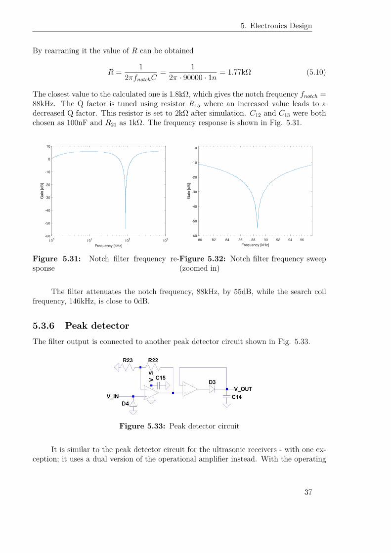
The closest value to the calculated one is 1.8kΩ, which gives the notch frequency fnotch =88kHz. The Q factor is tuned using resistor R15 where an increased value leads to adecreased Q factor. This resistor is set to 2kΩ after simulation. C12 and C13 were bothchosen as 100nF and R21 as 1kΩ. The frequency response is shown in Fig. 5.31.
100 101 102 103
Frequency [kHz]
-60
-50
-40
-30
-20
-10
0
10
Gain
[dB
]
Figure 5.31: Notch filter frequency re-sponse
80 82 84 86 88 90 92 94 96
Frequency [kHz]
-60
-50
-40
-30
-20
-10
0
Gain
[dB
]
Figure 5.32: Notch filter frequency sweep(zoomed in)
The filter attenuates the notch frequency, 88kHz, by 55dB, while the search coilfrequency, 146kHz, is close to 0dB.
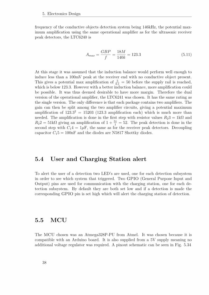
5.3.6 Peak detectorThe filter output is connected to another peak detector circuit shown in Fig. 5.33.
Figure 5.33: Peak detector circuit
It is similar to the peak detector circuit for the ultrasonic receivers - with one ex-ception; it uses a dual version of the operational amplifier instead. With the operating
37
5. Electronics Design
frequency of the conductive objects detection system being 146kHz, the potential max-imum amplification using the same operational amplifier as for the ultrasonic receiverpeak detectors, the LTC6240 is
Amax = GBP
f= 18M
140k = 123.3 (5.11)
At this stage it was assumed that the induction balance would perform well enough toinduce less than a 100mV peak at the receiver end with no conductive object present.This gives a potential max amplification of 5
0.1 = 50 before the supply rail is reached,which is below 123.3. However with a better induction balance, more amplification couldbe possible. It was thus deemed desirable to have more margin. Therefore the dualversion of the operational amplifier, the LTC6241 was chosen. It has the same rating asthe single version. The only difference is that each package contains two amplifiers. Thegain can then be split among the two amplifier circuits, giving a potential maximumamplification of 123.32 = 15203 (123.3 amplification each) which is much more thanneeded. The amplification is done in the first step with resistor values R23 = 1kΩ andR22 = 51kΩ giving an amplification of 1 + 51
1 = 52. The peak detection is done in thesecond step with C14 = 1µF, the same as for the receiver peak detectors. Decouplingcapacitor C15 = 100nF and the diodes are N5817 Shottky diodes.
5.4 User and Charging Station alert
To alert the user of a detection two LED’s are used, one for each detection subsystemin order to see which system that triggered. Two GPIO (General Purpose Input andOutput) pins are used for communication with the charging station, one for each de-tection subsystem. By default they are both set low and if a detection is made thecorresponding GPIO pin is set high which will alert the charging station of detection.
5.5 MCU
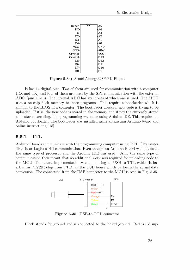
The MCU chosen was an Atmega328P-PU from Atmel. It was chosen because it iscompatible with an Arduino board. It is also supplied from a 5V supply meaning noadditional voltage regulator was required. A pinout schematic can be seen in Fig. 5.34
38
5. Electronics Design
Reset-
RX-
TX-
D2-
D3-
D4-
VCC-
GND-
Crystal-
Crystal-
D5-
D6-
D7-
D8-
-A5
-A4
-A3
-A2
-A1
-A0
-GND
-ARef
-VCC
-D13
-D12
-D11
-D10
-D9
Figure 5.34: Atmel Atmega328P-PU Pinout
It has 14 digital pins. Two of them are used for communication with a computer(RX and TX) and four of them are used by the SPI communication with the externalADC (pins 10-13). The internal ADC has six inputs of which one is used. The MCUuses a on-chip flash memory to store programs. This require a bootloader which issimiliar to the BIOS in a computer. The bootloader checks if new code is trying to beuploaded. If it is, the new code is stored in the memory and if not the currently storedcode starts executing. The programming was done using Arduino IDE. This requires anArduino bootloader. The bootloader was installed using an existing Arduino board andonline instructions, [15].
5.5.1 TTLArduino Boards communicate with the programming computer using TTL, (TransistorTransistor Logic) serial communication. Even though an Arduino Board was not used,the same type of processor and the Arduino IDE was used. Using the same type ofcommunication then meant that no additional work was required for uploading code tothe MCU. The actual implementation was done using an USB-to-TTL cable. It hasa builtin FT232R chip from FTDI in the USB house which performs the actual dataconversion. The connection from the USB connector to the MCU is seen in Fig. 5.35
Black
Brown
Red
Orange
Yellow
Green
TTL Header
NC
MCU
Reset
TX
RX
C
USB
Figure 5.35: USB-to-TTL connector
Black stands for ground and is connected to the board ground. Red is 5V sup-
39
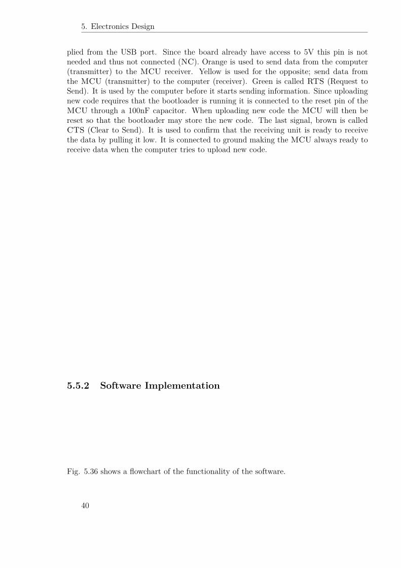
5. Electronics Design
plied from the USB port. Since the board already have access to 5V this pin is notneeded and thus not connected (NC). Orange is used to send data from the computer(transmitter) to the MCU receiver. Yellow is used for the opposite; send data fromthe MCU (transmitter) to the computer (receiver). Green is called RTS (Request toSend). It is used by the computer before it starts sending information. Since uploadingnew code requires that the bootloader is running it is connected to the reset pin of theMCU through a 100nF capacitor. When uploading new code the MCU will then bereset so that the bootloader may store the new code. The last signal, brown is calledCTS (Clear to Send). It is used to confirm that the receiving unit is ready to receivethe data by pulling it low. It is connected to ground making the MCU always ready toreceive data when the computer tries to upload new code.
5.5.2 Software Implementation
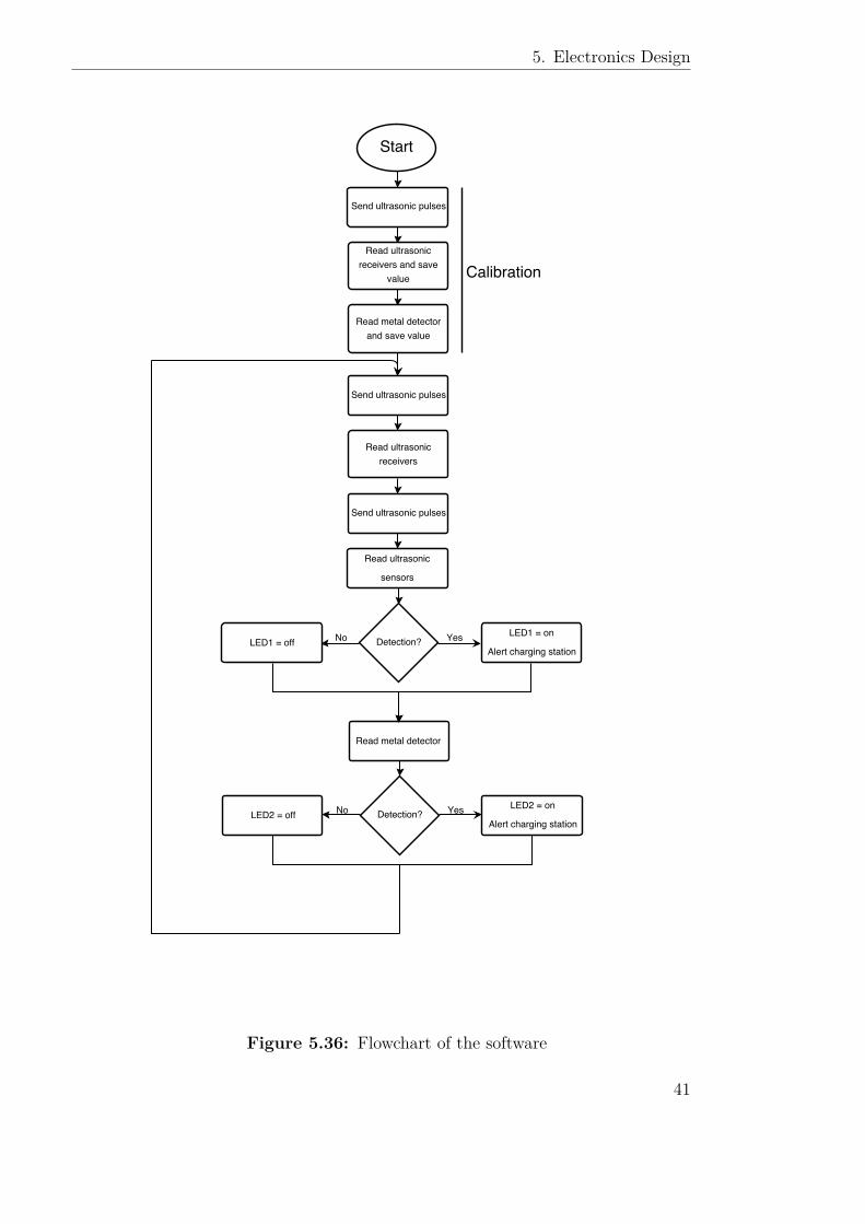
Fig. 5.36 shows a flowchart of the functionality of the software.
40
5. Electronics Design
Figure 5.36: Flowchart of the software
41
5. Electronics Design
When the system is powered up calibration of the conductive objects detector andthe ultrasonic tripwires is performed. First 20 samples from the conductive objectsdetection system is read, and the mean value of those, is saved as the zero level of themetal detector. The same process is then made for the 16 ultrasonic tripwires.
Then the main loop of the program begins. Every loop, the outputs from theconductive objects detector and the receivers are compared with the saved zero levels.The last four differences are summed. If the difference in any case is larger than thethreshold, a detection is reported. The ultrasonic distance sensors measure the distanceto the closest object. If any object is closer than 170 cm a detection is reported. If adetection is made, one of the LEDs are switched on and on of the GPIO pins are sethigh depending on which subsystem that registered a detection, ultrasonic or conductiveobjects.
For testing purposes, the program is able to send data over the TTL cable back toa computer. This in order to make it easier to evaluate the system.
5.6 PCB Layout
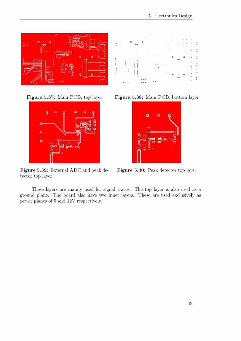
With the circuitry design completed and component choice made, a PCB layout wascreated. On the PCB all components was placed and traces drawn between them.The layout was designed manually using Altium Designer. There exist some generalguidelines for designing a PCB layout, for example [14]. However there are no consensusregarding an optimal design and greatly varies from one designer to another. Fig. 5.37-5.40 shows the top and bottom layer of the different PCB’s.
42
5. Electronics Design
PAC101 PAC102 COC1
PAC202 PAC201
COC2
PAC302
PAC301
COC3
PAC402
PAC401
COC4 PAC501
PAC502
COC5
PAC601
PAC602
COC6
PAC702
PAC701
COC7
PAC801 PAC802 COC8
PAC901 PAC902
COC9 PAC1001
PAC1002
COC10
PAC1101 PAC1102
COC11
PAC1201 PAC1202
COC12
PAC1301
PAC1302 COC13
PAC1401 PAC1402
COC14 PAC1501 PAC1502
COC15
PAC1601
PAC1602
COC16
PAC1701 PAC1702
COC17
PAC1801
PAC1802
COC18
PAC1901 PAC1902
COC19
PAC2001
PAC2002
COC20 PAC2101 PAC2102
COC21
PAC2401
PAC2402
COC24
PAC2501 PAC2502 COC25
PAD101
PAD102
COD1
PAD202 PAD201
COD2
PAD302 PAD301
COD3
PAD601
PAD602
COD6
PAIC103 PAIC102 PAIC101
COIC1
PAIC208
PAIC207
PAIC206
PAIC205 PAIC204
PAIC203
PAIC202
PAIC201
COIC2
PAIC308
PAIC307
PAIC306
PAIC305 PAIC304
PAIC303
PAIC302
PAIC301
COIC3
PAIC408
PAIC407
PAIC406
PAIC405 PAIC404
PAIC403
PAIC402
PAIC401
COIC4 PAJ102
PAJ101
COJ1
PAJ202
PAJ201
COJ2
PAJ302
PAJ301
COJ3
PAJ402
PAJ401
COJ4
PAJ501
COJ5
PAJ601
COJ6
PAJ701
COJ7
PAJ801
COJ8
PAJ902
PAJ901
COJ9
PAJ1002
PAJ1001
COJ10
PAJ1101
COJ11
PAJ1201
COJ12
PAJ1301
COJ13
PAJ14028
PAJ14015
PAJ14027
PAJ14026
PAJ14025
PAJ14024
PAJ14023
PAJ14022
PAJ14021
PAJ14020
PAJ14019
PAJ14018
PAJ14017
PAJ14016 PAJ14013
PAJ14012
PAJ14011
PAJ14010
PAJ1409
PAJ1408
PAJ1407
PAJ1406
PAJ1405
PAJ1404
PAJ1403
PAJ1402
PAJ1401
PAJ14014
COJ14
PAJ1501
COJ15
PAJ1901 PAJ1902 PAJ1903
PAJ1904 PAJ1905 PAJ1906
COJ19
PAJ2002 PAJ2001 COJ20
PAJ2102 PAJ2101 COJ21
PAJ2201
COJ22
PAJ2701
PAJ2702
PAJ2703
PAJ2704
PAJ2705
PAJ2706
COJ27
PAJ2801
PAJ2802
COJ28
PAJ2902
PAJ2901
COJ29
PAJ3001
COJ30
PAJ3101
COJ31
PAJ3201
COJ32
PAJ3301
COJ33
PAJ3401
COJ34
PAJ3501
COJ35
PAJ3601
COJ36
PAJ3701
COJ37
PAJ3801
COJ38
PAJ3901
COJ39
PAJ4001
COJ40
PAJ4101
COJ41
PAL101 PAL102 COL1
PAMP10
COMP1
PAMP20
COMP2
PAMP30
COMP3
PAQ103 PAQ102 PAQ101
COQ1
PAQ203 PAQ202 PAQ201
COQ2
PAR102
PAR101
COR1
PAR202 PAR201
COR2
PAR302 PAR301
COR3 PAR402
PAR401
COR4
PAR502
PAR501
COR5
PAR602
PAR601
COR6
PAR702 PAR701
COR7
PAR802 PAR801
COR8 PAR902 PAR901
COR9
PAR1002 PAR1001 COR10
PAR1102 PAR1101
COR11
PAR1202 PAR1201
COR12
PAR1302
PAR1301
COR13 PAR1402
PAR1401
COR14
PAR1502
PAR1501
COR15
PAR1602
PAR1601
COR16
PAR1702
PAR1701
COR17 PAR1802
PAR1801
COR18
PAR1902
PAR1901
COR19
PAR2002
PAR2001
COR20
PAR2102 PAR2101
COR21
PAR2202
PAR2201
COR22
PAR2302 PAR2301
COR23
PAR2402 PAR2401
COR24
PAR2502 PAR2501
COR25
PAR2602
PAR2601
COR26
PAR2702
PAR2701
COR27
PAR2802 PAR2801
COR28
PAR2902
PAR2901
COR29
PAR3002
PAR3001
COR30
PAR3102 PAR3101
COR31
PAR3202
PAR3201
COR32 PAR3302
PAR3301
COR33 PAR4002 PAR4001
COR40
PAR4102 PAR4101
COR41
PAR4202
PAR4201
COR42
PAR4302
PAR4301
COR43
PAX102
PAX101
COX1
PAC201
PAC501
PAC1301
PAC2001
PAIC103
PAIC308
PAIC408
PAJ1407
PAJ1906 PAJ2002
PAR501
PAR2301
PAR2601
PAR4201
PAC301
PAC1001
PAC2501
PAIC208
PAJ2802
PAQ102
PAR701
PAR802
PAR4001
PAC101
PAC202
PAC302
PAC402 PAC502
PAC602
PAC701
PAC902
PAC1002
PAC1102 PAC1201
PAC1302
PAC1802
PAC1902
PAC2002 PAC2102
PAC2502
PAD101
PAD302
PAD601
PAIC102
PAIC204
PAIC304
PAIC404
PAJ601
PAJ1408
PAJ14022
PAJ1905 PAJ2001
PAJ2701
PAJ2702
PAJ2801
PAJ3601
PAJ3701
PAQ202
PAR101
PAR902
PAR1002
PAR1202
PAR2002
PAR2502
PAR2701
PAR2801
PAR2902
PAR3302
PAR4102
PAC102
PAIC101
PAR4002
PAR4101
PAC401
PAJ1409
PAX102 PAC601
PAJ14020
PAJ14021 PAR502
PAC702 PAJ14010 PAX101
PAC801
PAC1202
PAIC201
PAL102
PAR1401
PAC802
PAIC205
PAR702
PAR1001
PAC901 PAIC203
PAR801
PAR901
PAC1101
PAL101 PAR1302
PAC1401
PAC1502
PAR1502 PAR1701
PAC1402
PAIC303
PAR1501 PAR1801
PAC1601
PAIC301
PAR1602 PAR2101
PAC1701 PAIC307
PAR2202
PAC1702
PAR1802
PAC1801 PAR1902
PAC1901
PAIC305 PAR2302
PAR2402
PAR2501
PAC2401 PAJ1401 PAR4202
PAC2402
PAJ2706
PAD102
PAR602
PAD202 PAIC407
PAD602
PAR4302
PAIC202
PAR1301
PAR1402
PAIC206 PAR1102
PAR1201
PAIC207
PAQ101
PAQ201
PAR1101
PAIC302
PAR1601 PAR1901
PAIC306
PAR1702 PAR2201
PAIC401
PAIC405
PAR3001
PAIC402
PAR2702 PAR3002
PAIC406
PAR2802
PAR3102
PAJ101 PAJ1101
PAR201
PAR301
PAJ102
PAJ301
PAJ501
PAJ201 PAJ801
PAJ202
PAJ902
PAJ2902
PAQ103
PAQ203
PAJ302
PAJ401
PAJ3001 PAJ402
PAJ3101
PAJ701 PAJ3801
PAJ901 PAJ3401
PAJ1001
PAJ1404
PAJ1002
PAJ1405
PAJ1201
PAJ4101
PAR102
PAJ1301
PAJ1406
PAJ1402 PAJ2704
PAJ1403 PAJ2705
PAJ14011
PAJ2101
PAJ14012
PAJ2102
PAJ14013
PAJ2201
PAJ14014
PAR601
PAJ14015
PAR4301
PAJ14016
PAJ1904
PAJ14017
PAJ1901
PAJ14018
PAJ1902
PAJ14019
PAJ1903
PAC2101
PAD201
PAJ14023
PAJ1501
PAR3101
PAJ2901 PAJ3501
PAJ3201 PAJ3901
PAJ3301 PAJ4001
PAC1501
PAR202
PAD301
PAIC403
PAR302 PAR401
PAR3202 PAR3301
PAC1602 PAR402 PAR2001
PAR2102
PAR2401
PAR2602 PAR2901 PAR3201
Figure 5.37: Main PCB, top layer
PAC101 PAC102 COC1
PAC202 PAC201
COC2
PAC302
PAC301
COC3
PAC402
PAC401
COC4 PAC501
PAC502
COC5
PAC601
PAC602
COC6
PAC702
PAC701
COC7
PAC801 PAC802 COC8
PAC901 PAC902
COC9 PAC1001
PAC1002
COC10
PAC1101 PAC1102
COC11
PAC1201 PAC1202
COC12
PAC1301
PAC1302 COC13
PAC1401 PAC1402
COC14 PAC1501 PAC1502
COC15
PAC1601
PAC1602
COC16
PAC1701 PAC1702
COC17
PAC1801
PAC1802
COC18
PAC1901 PAC1902
COC19
PAC2001
PAC2002
COC20 PAC2101 PAC2102
COC21
PAC2401
PAC2402
COC24
PAC2501 PAC2502 COC25
PAD101
PAD102
COD1
PAD202 PAD201
COD2
PAD302 PAD301
COD3
PAD601
PAD602
COD6
PAIC103 PAIC102 PAIC101
COIC1
PAIC208
PAIC207
PAIC206
PAIC205 PAIC204
PAIC203
PAIC202
PAIC201
COIC2
PAIC308
PAIC307
PAIC306
PAIC305 PAIC304
PAIC303
PAIC302
PAIC301
COIC3
PAIC408
PAIC407
PAIC406
PAIC405 PAIC404
PAIC403
PAIC402
PAIC401
COIC4 PAJ102
PAJ101
COJ1
PAJ202
PAJ201
COJ2
PAJ302
PAJ301
COJ3
PAJ402
PAJ401
COJ4
PAJ501
COJ5
PAJ601
COJ6
PAJ701
COJ7
PAJ801
COJ8
PAJ902
PAJ901
COJ9
PAJ1002
PAJ1001
COJ10
PAJ1101
COJ11
PAJ1201
COJ12
PAJ1301
COJ13
PAJ14028
PAJ14015
PAJ14027
PAJ14026
PAJ14025
PAJ14024
PAJ14023
PAJ14022
PAJ14021
PAJ14020
PAJ14019
PAJ14018
PAJ14017
PAJ14016 PAJ14013
PAJ14012
PAJ14011
PAJ14010
PAJ1409
PAJ1408
PAJ1407
PAJ1406
PAJ1405
PAJ1404
PAJ1403
PAJ1402
PAJ1401
PAJ14014
COJ14
PAJ1501
COJ15
PAJ1901 PAJ1902 PAJ1903
PAJ1904 PAJ1905 PAJ1906
COJ19
PAJ2002 PAJ2001 COJ20
PAJ2102 PAJ2101 COJ21
PAJ2201
COJ22
PAJ2701
PAJ2702
PAJ2703
PAJ2704
PAJ2705
PAJ2706
COJ27
PAJ2801
PAJ2802
COJ28
PAJ2902
PAJ2901
COJ29
PAJ3001
COJ30
PAJ3101
COJ31
PAJ3201
COJ32
PAJ3301
COJ33
PAJ3401
COJ34
PAJ3501
COJ35
PAJ3601
COJ36
PAJ3701
COJ37
PAJ3801
COJ38
PAJ3901
COJ39
PAJ4001
COJ40
PAJ4101
COJ41
PAL101 PAL102 COL1
PAMP10
COMP1
PAMP20
COMP2
PAMP30
COMP3
PAQ103 PAQ102 PAQ101
COQ1
PAQ203 PAQ202 PAQ201
COQ2
PAR102
PAR101
COR1
PAR202 PAR201
COR2
PAR302 PAR301
COR3 PAR402
PAR401
COR4
PAR502
PAR501
COR5
PAR602
PAR601
COR6
PAR702 PAR701
COR7
PAR802 PAR801
COR8 PAR902 PAR901
COR9
PAR1002 PAR1001 COR10
PAR1102 PAR1101
COR11
PAR1202 PAR1201
COR12
PAR1302
PAR1301
COR13 PAR1402
PAR1401
COR14
PAR1502
PAR1501
COR15
PAR1602
PAR1601
COR16
PAR1702
PAR1701
COR17 PAR1802
PAR1801
COR18
PAR1902
PAR1901
COR19
PAR2002
PAR2001
COR20
PAR2102 PAR2101
COR21
PAR2202
PAR2201
COR22
PAR2302 PAR2301
COR23
PAR2402 PAR2401
COR24
PAR2502 PAR2501
COR25
PAR2602
PAR2601
COR26
PAR2702
PAR2701
COR27
PAR2802 PAR2801
COR28
PAR2902
PAR2901
COR29
PAR3002
PAR3001
COR30
PAR3102 PAR3101
COR31
PAR3202
PAR3201
COR32 PAR3302
PAR3301
COR33 PAR4002 PAR4001
COR40
PAR4102 PAR4101
COR41
PAR4202
PAR4201
COR42
PAR4302
PAR4301
COR43
PAX102
PAX101
COX1
PAC201
PAC501
PAC1301
PAC2001
PAIC103
PAIC308
PAIC408
PAJ1407
PAJ1906 PAJ2002
PAR501
PAR2301
PAR2601
PAR4201
PAC301
PAC1001
PAC2501
PAIC208
PAJ2802
PAQ102
PAR701
PAR802
PAR4001
PAC101
PAC202
PAC302
PAC402 PAC502
PAC602
PAC701
PAC902
PAC1002
PAC1102 PAC1201
PAC1302
PAC1802
PAC1902
PAC2002 PAC2102
PAC2502
PAD101
PAD302
PAD601
PAIC102
PAIC204
PAIC304
PAIC404
PAJ601
PAJ1408
PAJ14022
PAJ1905 PAJ2001
PAJ2701
PAJ2702
PAJ2801
PAJ3601
PAJ3701
PAQ202
PAR101
PAR902
PAR1002
PAR1202
PAR2002
PAR2502
PAR2701
PAR2801
PAR2902
PAR3302
PAR4102
PAC102
PAIC101
PAR4002
PAR4101
PAC401
PAJ1409
PAX102 PAC601
PAJ14020
PAJ14021 PAR502
PAC702 PAJ14010 PAX101
PAC801
PAC1202
PAIC201
PAL102
PAR1401
PAC802
PAIC205
PAR702
PAR1001
PAC901 PAIC203
PAR801
PAR901
PAC1101
PAL101 PAR1302
PAC1401
PAC1502
PAR1502 PAR1701
PAC1402
PAIC303
PAR1501 PAR1801
PAC1601
PAIC301
PAR1602 PAR2101
PAC1701 PAIC307
PAR2202
PAC1702
PAR1802
PAC1801 PAR1902
PAC1901
PAIC305 PAR2302
PAR2402
PAR2501
PAC2401 PAJ1401 PAR4202
PAC2402
PAJ2706
PAD102
PAR602
PAD202 PAIC407
PAD602
PAR4302
PAIC202
PAR1301
PAR1402
PAIC206 PAR1102
PAR1201
PAIC207
PAQ101
PAQ201
PAR1101
PAIC302
PAR1601 PAR1901
PAIC306
PAR1702 PAR2201
PAIC401
PAIC405
PAR3001
PAIC402
PAR2702 PAR3002
PAIC406
PAR2802
PAR3102
PAJ101 PAJ1101
PAR201
PAR301
PAJ102
PAJ301
PAJ501
PAJ201 PAJ801
PAJ202
PAJ902
PAJ2902
PAQ103
PAQ203
PAJ302
PAJ401
PAJ3001 PAJ402
PAJ3101
PAJ701 PAJ3801
PAJ901 PAJ3401
PAJ1001
PAJ1404
PAJ1002
PAJ1405
PAJ1201
PAJ4101
PAR102
PAJ1301
PAJ1406
PAJ1402 PAJ2704
PAJ1403 PAJ2705
PAJ14011
PAJ2101
PAJ14012
PAJ2102
PAJ14013
PAJ2201
PAJ14014
PAR601
PAJ14015
PAR4301
PAJ14016
PAJ1904
PAJ14017
PAJ1901
PAJ14018
PAJ1902
PAJ14019
PAJ1903
PAC2101
PAD201
PAJ14023
PAJ1501
PAR3101
PAJ2901 PAJ3501
PAJ3201 PAJ3901
PAJ3301 PAJ4001
PAC1501
PAR202
PAD301
PAIC403
PAR302 PAR401
PAR3202 PAR3301
PAC1602 PAR402 PAR2001
PAR2102
PAR2401
PAR2602 PAR2901 PAR3201
Figure 5.38: Main PCB, bottom layer
PAC220PDS101
PAC220PDS102
COC220PDS1
PAC230PDS101
PAC230PDS102 COC230PDS1 PAD40PDS102 PAD40PDS101
COD40PDS1
PAD50PDS102 PAD50PDS101 COD50PDS1
PAIC501 PAIC502 PAIC503 PAIC504 PAIC505 PAIC506 PAIC507
PAIC508 PAIC509 PAIC5010 PAIC5011 PAIC5012 PAIC5013 PAIC5014 COIC5
PAIC60PDS108
PAIC60PDS107
PAIC60PDS106
PAIC60PDS105 PAIC60PDS104
PAIC60PDS103
PAIC60PDS102
PAIC60PDS101
COIC60PDS1
PAJ2302 PAJ2301 PAJ2303
COJ23
PAJ2402 PAJ2401 PAJ2403
COJ24
PAJ2502
PAJ2501
PAJ2503
COJ25
PAJ2601
PAJ2602
PAJ2603
PAJ2604
PAJ2605
PAJ2606
COJ26
PAR340PDS102
PAR340PDS101 COR340PDS1 PAR350PDS101
PAR350PDS102
COR350PDS1
PAR360PDS102
PAR360PDS101
COR360PDS1 PAR370PDS102
PAR370PDS101
COR370PDS1 PAR380PDS102
PAR380PDS101
COR380PDS1 PAR390PDS102
PAR390PDS101 COR390PDS1 PAC220PDS101
PAIC5013 PAIC5014
PAIC60PDS107
PAJ2303 PAJ2403
PAJ2503
PAJ2606
PAR340PDS101 PAC220PDS102
PAC230PDS102
PAD50PDS102
PAIC507
PAIC5012
PAIC60PDS104
PAJ2302 PAJ2402
PAJ2502
PAJ2605
PAR350PDS101
PAR360PDS102
PAR390PDS102
PAC230PDS101 PAD40PDS101
PAIC504
PAR370PDS101
PAD40PDS102 PAIC60PDS106
PAD50PDS101
PAIC60PDS103
PAR380PDS102 PAR390PDS101
PAIC501
PAJ2301
PAIC502
PAJ2401
PAIC503
PAJ2501 PAIC508
PAJ2604 PAIC509
PAJ2601 PAIC5010 PAJ2602 PAIC5011
PAJ2603
PAIC60PDS102
PAR350PDS102 PAR370PDS102
PAR340PDS102 PAR360PDS101
PAR380PDS101
Figure 5.39: External ADC and peak de-tector top layer
PAC220PDS201
PAC220PDS202
COC220PDS2
PAC230PDS201
PAC230PDS202 COC230PDS2 PAD40PDS202 PAD40PDS201
COD40PDS2
PAD50PDS202 PAD50PDS201 COD50PDS2 PAIC60PDS208
PAIC60PDS207
PAIC60PDS206
PAIC60PDS205 PAIC60PDS204
PAIC60PDS203
PAIC60PDS202
PAIC60PDS201
COIC60PDS2
PAJ1602 PAJ1601 PAJ1603
COJ16
PAR340PDS202
PAR340PDS201 COR340PDS2 PAR350PDS201
PAR350PDS202
COR350PDS2
PAR360PDS202
PAR360PDS201
COR360PDS2 PAR370PDS202
PAR370PDS201
COR370PDS2 PAR380PDS202
PAR380PDS201
COR380PDS2 PAR390PDS202
PAR390PDS201 COR390PDS2 PAC220PDS201 PAIC60PDS207
PAJ1603
PAR340PDS201 PAC220PDS202
PAC230PDS202
PAD50PDS202
PAIC60PDS204
PAJ1602
PAR350PDS201
PAR360PDS202
PAR390PDS202
PAD40PDS202 PAIC60PDS206
PAD50PDS201
PAIC60PDS203
PAR380PDS202 PAR390PDS201
PAIC60PDS202
PAR350PDS202 PAR370PDS202
PAC230PDS201 PAD40PDS201
PAJ1601
PAR370PDS201
PAR340PDS202 PAR360PDS201
PAR380PDS201
Figure 5.40: Peak detector top layer
These layers are mainly used for signal traces. The top layer is also used as aground plane. The board also have two inner layers. These are used exclusively aspower planes of 5 and 12V respectively.
43

5. Electronics Design
44
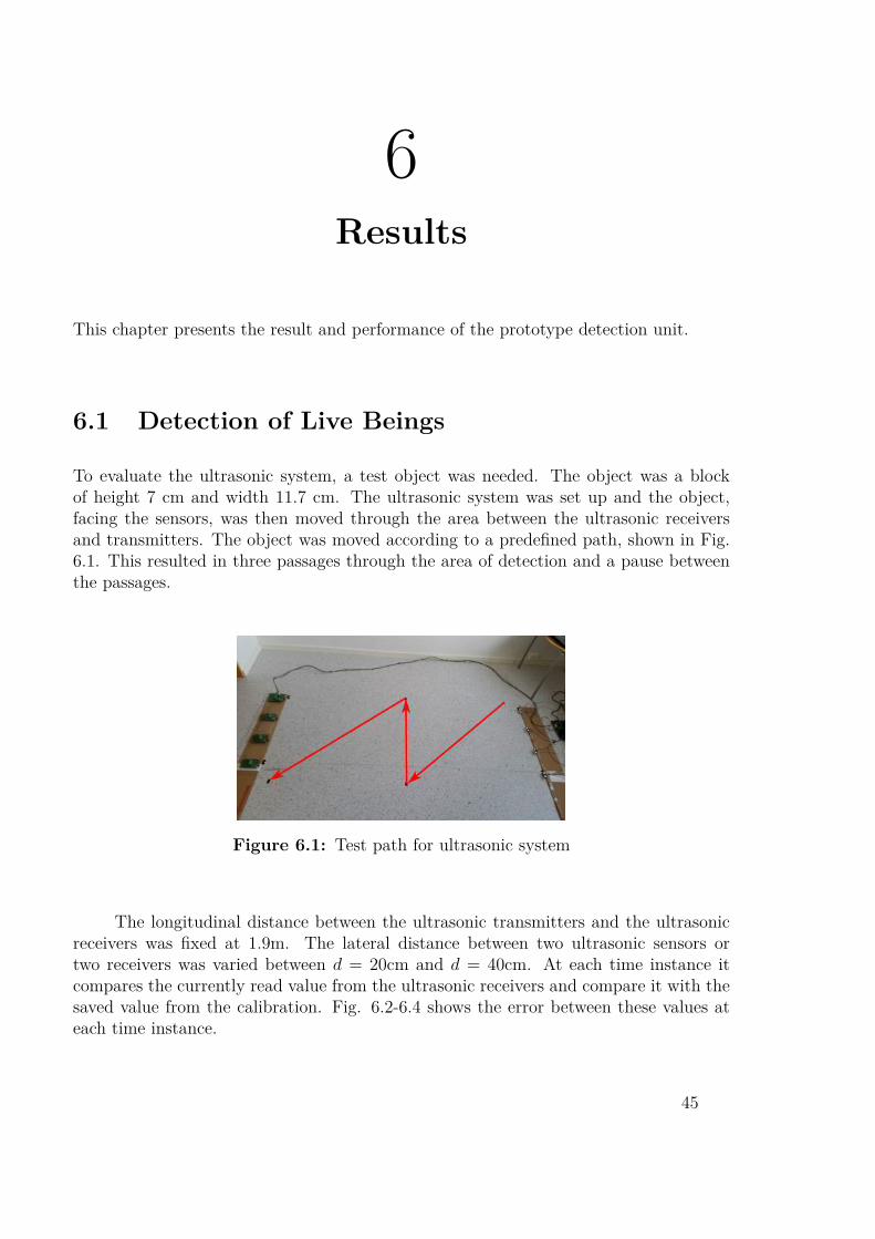
6Results
This chapter presents the result and performance of the prototype detection unit.
6.1 Detection of Live Beings
To evaluate the ultrasonic system, a test object was needed. The object was a blockof height 7 cm and width 11.7 cm. The ultrasonic system was set up and the object,facing the sensors, was then moved through the area between the ultrasonic receiversand transmitters. The object was moved according to a predefined path, shown in Fig.6.1. This resulted in three passages through the area of detection and a pause betweenthe passages.
Figure 6.1: Test path for ultrasonic system
The longitudinal distance between the ultrasonic transmitters and the ultrasonicreceivers was fixed at 1.9m. The lateral distance between two ultrasonic sensors ortwo receivers was varied between d = 20cm and d = 40cm. At each time instance itcompares the currently read value from the ultrasonic receivers and compare it with thesaved value from the calibration. Fig. 6.2-6.4 shows the error between these values ateach time instance.
45
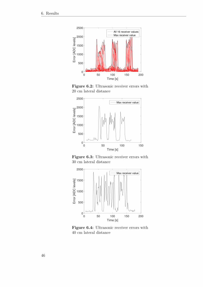
6. Results
0 50 100 150 200
Time [s]
0
500
1000
1500
2000
2500
Err
or
[AD
C le
ve
ls]
All 16 receiver values
Max receiver value
Figure 6.2: Ultrasonic receiver errors with20 cm lateral distance
0 50 100 150
Time [s]
0
500
1000
1500
2000
2500
Err
or
[AD
C le
ve
ls]
Max receiver value
Figure 6.3: Ultrasonic receiver errors with30 cm lateral distance
0 50 100 150 200
Time [s]
0
500
1000
1500
2000
Err
or
[AD
C le
ve
ls]
Max receiver value
Figure 6.4: Ultrasonic receiver errors with40 cm lateral distance
46
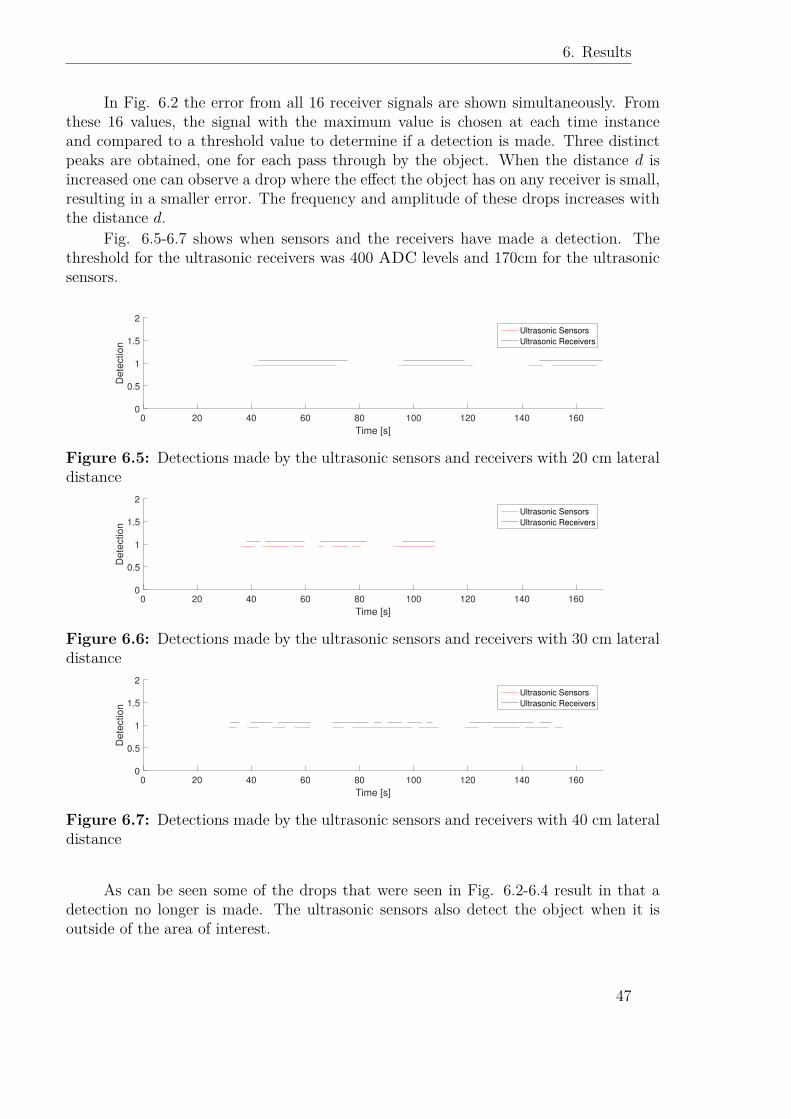
6. Results
In Fig. 6.2 the error from all 16 receiver signals are shown simultaneously. Fromthese 16 values, the signal with the maximum value is chosen at each time instanceand compared to a threshold value to determine if a detection is made. Three distinctpeaks are obtained, one for each pass through by the object. When the distance d isincreased one can observe a drop where the effect the object has on any receiver is small,resulting in a smaller error. The frequency and amplitude of these drops increases withthe distance d.
Fig. 6.5-6.7 shows when sensors and the receivers have made a detection. Thethreshold for the ultrasonic receivers was 400 ADC levels and 170cm for the ultrasonicsensors.
0 20 40 60 80 100 120 140 160
Time [s]
0
0.5
1
1.5
2
De
tectio
n
Ultrasonic Sensors
Ultrasonic Receivers
Figure 6.5: Detections made by the ultrasonic sensors and receivers with 20 cm lateraldistance
0 20 40 60 80 100 120 140 160
Time [s]
0
0.5
1
1.5
2
De
tectio
n
Ultrasonic Sensors
Ultrasonic Receivers
Figure 6.6: Detections made by the ultrasonic sensors and receivers with 30 cm lateraldistance
0 20 40 60 80 100 120 140 160
Time [s]
0
0.5
1
1.5
2
De
tectio
n
Ultrasonic Sensors
Ultrasonic Receivers
Figure 6.7: Detections made by the ultrasonic sensors and receivers with 40 cm lateraldistance
As can be seen some of the drops that were seen in Fig. 6.2-6.4 result in that adetection no longer is made. The ultrasonic sensors also detect the object when it isoutside of the area of interest.
47
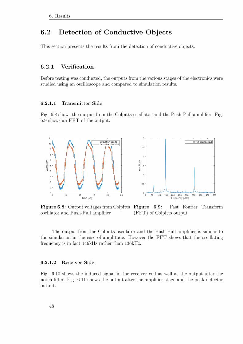
6. Results
6.2 Detection of Conductive Objects
This section presents the results from the detection of conductive objects.
6.2.1 Verification
Before testing was conducted, the outputs from the various stages of the electronics werestudied using an oscilloscope and compared to simulation results.
6.2.1.1 Transmitter Side
Fig. 6.8 shows the output from the Colpitts oscillator and the Push-Pull amplifier. Fig.6.9 shows an FFT of the output.
Time [µs]
0 5 10 15 20 25
Vo
lta
ge
[V
]
1
2
3
4
5
6
7
8
9
10
11
Output from Colpitts
Output from Push-Pull
Figure 6.8: Output voltages from Colpittsoscillator and Push-Pull amplifier
Frequency [kHz]
0 50 100 150 200 250 300 350 400 450 500
Am
plit
ud
e
0
0.5
1
1.5
2
2.5
3
FFT of Colpitts output
Figure 6.9: Fast Fourier Transform(FFT) of Colpitts output
The output from the Colpitts oscillator and the Push-Pull amplifier is similar tothe simulation in the case of amplitude. However the FFT shows that the oscillatingfrequency is in fact 146kHz rather than 136kHz.
6.2.1.2 Receiver Side
Fig. 6.10 shows the induced signal in the receiver coil as well as the output after thenotch filter. Fig. 6.11 shows the output after the amplifier stage and the peak detectoroutput.
48
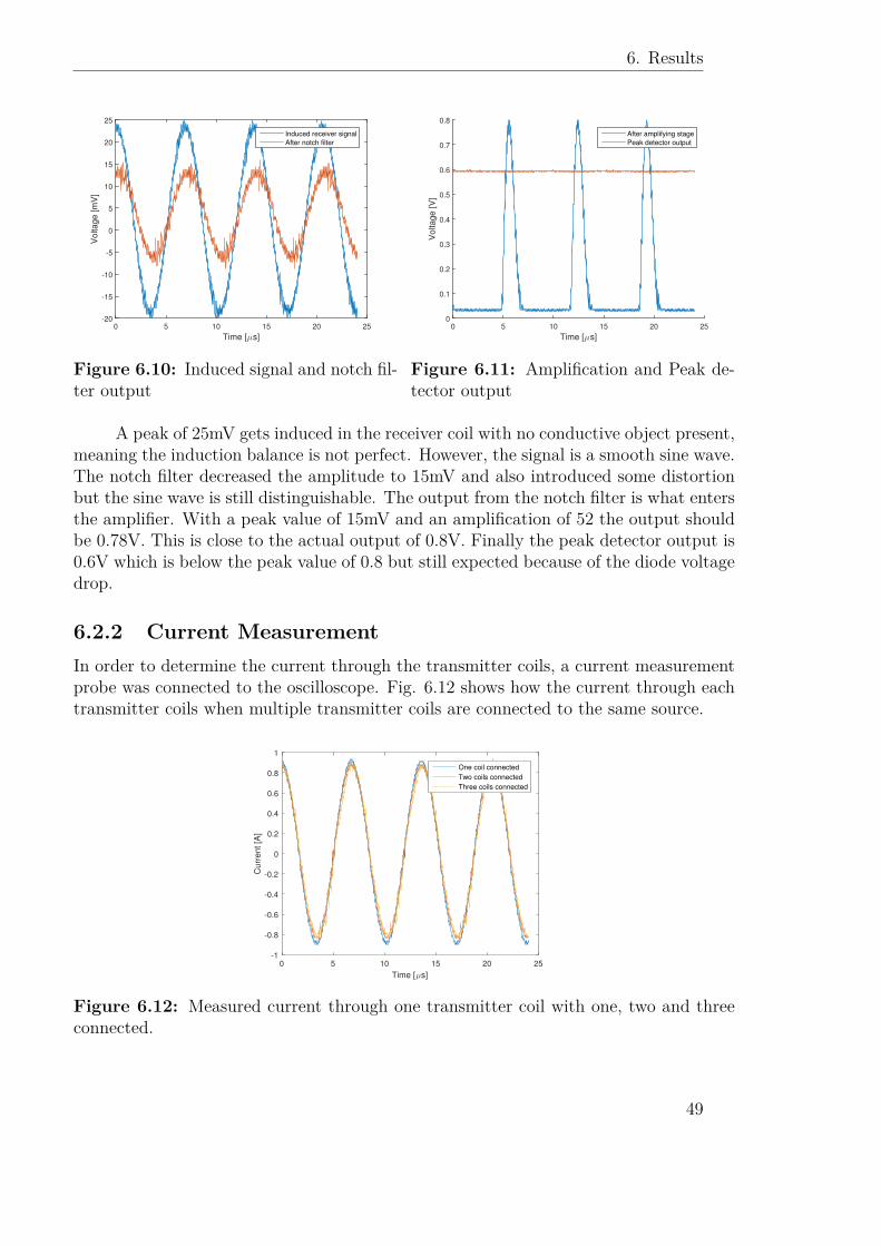
6. Results
Time [µs]
0 5 10 15 20 25
Vo
lta
ge
[m
V]
-20
-15
-10
-5
0
5
10
15
20
25
Induced receiver signal
After notch filter
Figure 6.10: Induced signal and notch fil-ter output
Time [µs]
0 5 10 15 20 25
Volta
ge
[V
]
0
0.1
0.2
0.3
0.4
0.5
0.6
0.7
0.8
After amplifying stage
Peak detector output
Figure 6.11: Amplification and Peak de-tector output
A peak of 25mV gets induced in the receiver coil with no conductive object present,meaning the induction balance is not perfect. However, the signal is a smooth sine wave.The notch filter decreased the amplitude to 15mV and also introduced some distortionbut the sine wave is still distinguishable. The output from the notch filter is what entersthe amplifier. With a peak value of 15mV and an amplification of 52 the output shouldbe 0.78V. This is close to the actual output of 0.8V. Finally the peak detector output is0.6V which is below the peak value of 0.8 but still expected because of the diode voltagedrop.
6.2.2 Current MeasurementIn order to determine the current through the transmitter coils, a current measurementprobe was connected to the oscilloscope. Fig. 6.12 shows how the current through eachtransmitter coils when multiple transmitter coils are connected to the same source.
0 5 10 15 20 25
Time [µs]
-1
-0.8
-0.6
-0.4
-0.2
0
0.2
0.4
0.6
0.8
1
Curr
ent [A
]
One coil connected
Two coils connected
Three coils connected
Figure 6.12: Measured current through one transmitter coil with one, two and threeconnected.
49
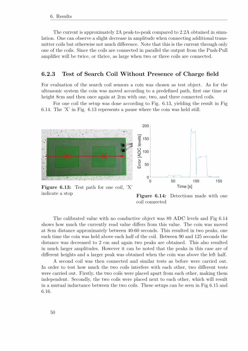
6. Results
The current is approximately 2A peak-to-peak compared to 2.2A obtained in simu-lation. One can observe a slight decrease in amplitude when connecting additional trans-mitter coils but otherwise not much difference. Note that this is the current through onlyone of the coils. Since the coils are connected in parallel the output from the Push-Pullamplifier will be twice, or thrice, as large when two or three coils are connected.
6.2.3 Test of Search Coil Without Presence of Charge field
For evaluation of the search coil sensors a coin was chosen as test object. As for theultrasonic system the coin was moved according to a predefined path, first one time atheight 8cm and then once again at 2cm with one, two, and three connected coils.
For one coil the setup was done according to Fig. 6.13, yielding the result in Fig6.14. The ’X’ in Fig. 6.13 represents a pause where the coin was held still.
Figure 6.13: Test path for one coil, ’X’indicate a stop
0 50 100 150
Time [s]
0
50
100
150
200
Err
or
[AD
C le
ve
ls]
Figure 6.14: Detections made with onecoil connected
The calibrated value with no conductive object was 89 ADC levels and Fig 6.14shows how much the currently read value differs from this value. The coin was movedat 8cm distance approximately between 40-60 seconds. This resulted in two peaks, oneeach time the coin was held above each half of the coil. Between 90 and 125 seconds thedistance was decreased to 2 cm and again two peaks are obtained. This also resultedin much larger amplitudes. However it can be noted that the peaks in this case are ofdifferent heights and a larger peak was obtained when the coin was above the left half.
A second coil was then connected and similar tests as before were carried out.In order to test how much the two coils interfere with each other, two different testswere carried out. Firstly, the two coils were placed apart from each other, making themindependent. Secondly, the two coils were placed next to each other, which will resultin a mutual inductance between the two coils. These setups can be seen in Fig 6.15 and6.16.
50
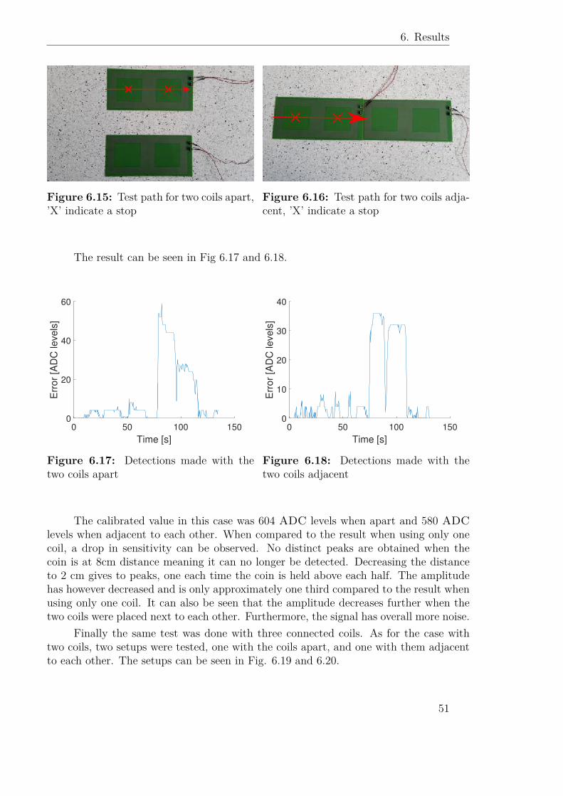
6. Results
Figure 6.15: Test path for two coils apart,’X’ indicate a stop
Figure 6.16: Test path for two coils adja-cent, ’X’ indicate a stop
The result can be seen in Fig 6.17 and 6.18.
0 50 100 150
Time [s]
0
20
40
60
Err
or
[AD
C le
ve
ls]
Figure 6.17: Detections made with thetwo coils apart
0 50 100 150
Time [s]
0
10
20
30
40
Err
or
[AD
C le
ve
ls]
Figure 6.18: Detections made with thetwo coils adjacent
The calibrated value in this case was 604 ADC levels when apart and 580 ADClevels when adjacent to each other. When compared to the result when using only onecoil, a drop in sensitivity can be observed. No distinct peaks are obtained when thecoin is at 8cm distance meaning it can no longer be detected. Decreasing the distanceto 2 cm gives to peaks, one each time the coin is held above each half. The amplitudehas however decreased and is only approximately one third compared to the result whenusing only one coil. It can also be seen that the amplitude decreases further when thetwo coils were placed next to each other. Furthermore, the signal has overall more noise.
Finally the same test was done with three connected coils. As for the case withtwo coils, two setups were tested, one with the coils apart, and one with them adjacentto each other. The setups can be seen in Fig. 6.19 and 6.20.
51
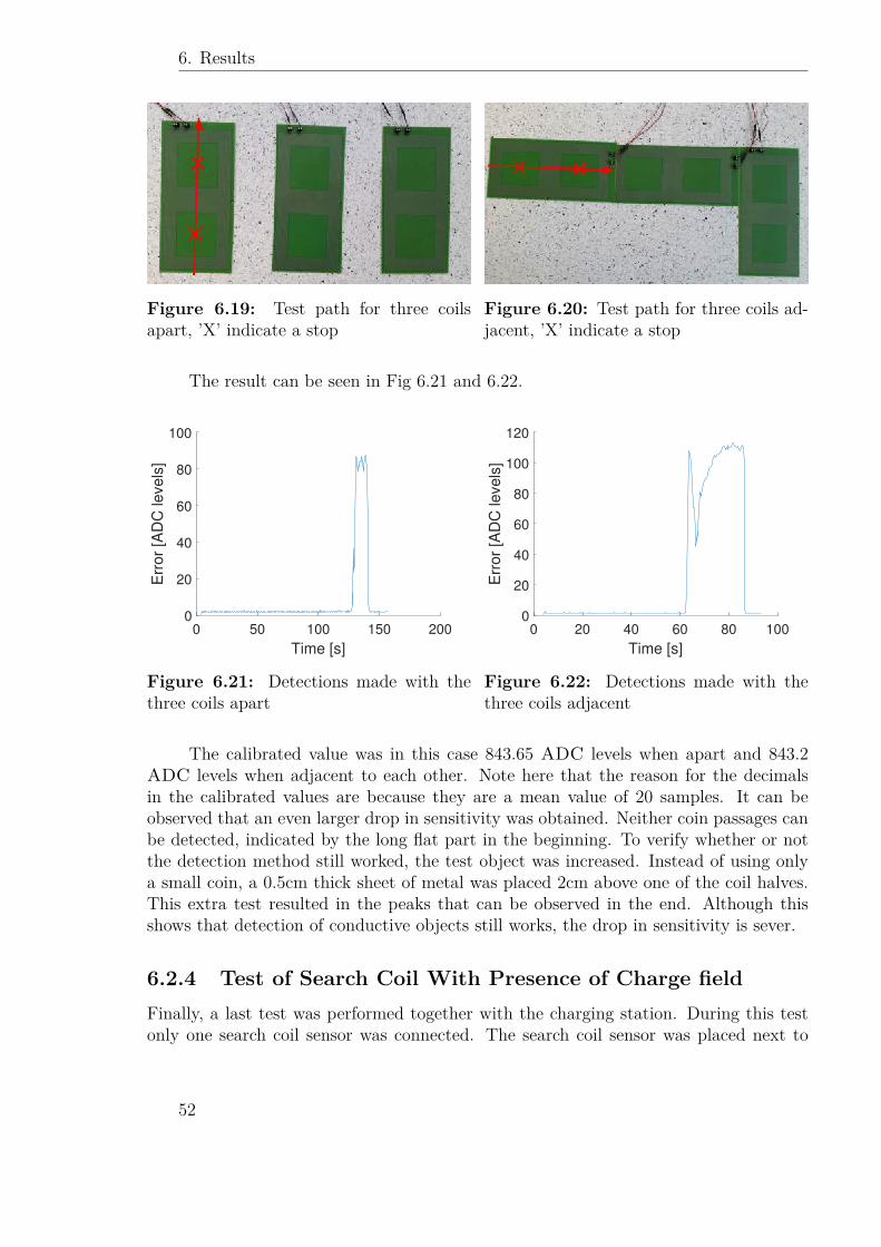
6. Results
Figure 6.19: Test path for three coilsapart, ’X’ indicate a stop
Figure 6.20: Test path for three coils ad-jacent, ’X’ indicate a stop
The result can be seen in Fig 6.21 and 6.22.
0 50 100 150 200
Time [s]
0
20
40
60
80
100
Err
or
[AD
C le
ve
ls]
Figure 6.21: Detections made with thethree coils apart
0 20 40 60 80 100
Time [s]
0
20
40
60
80
100
120
Err
or
[AD
C le
ve
ls]
Figure 6.22: Detections made with thethree coils adjacent
The calibrated value was in this case 843.65 ADC levels when apart and 843.2ADC levels when adjacent to each other. Note here that the reason for the decimalsin the calibrated values are because they are a mean value of 20 samples. It can beobserved that an even larger drop in sensitivity was obtained. Neither coin passages canbe detected, indicated by the long flat part in the beginning. To verify whether or notthe detection method still worked, the test object was increased. Instead of using onlya small coin, a 0.5cm thick sheet of metal was placed 2cm above one of the coil halves.This extra test resulted in the peaks that can be observed in the end. Although thisshows that detection of conductive objects still works, the drop in sensitivity is sever.
6.2.4 Test of Search Coil With Presence of Charge fieldFinally, a last test was performed together with the charging station. During this testonly one search coil sensor was connected. The search coil sensor was placed next to
52
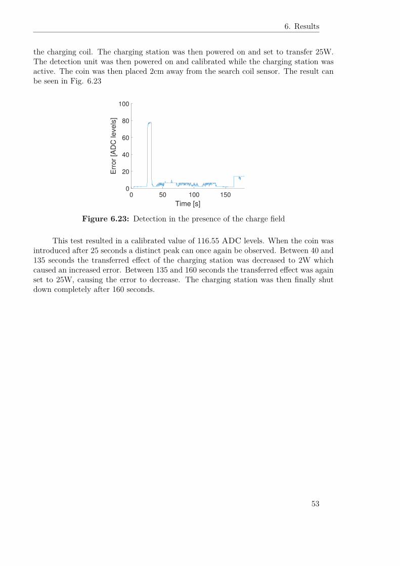
6. Results
the charging coil. The charging station was then powered on and set to transfer 25W.The detection unit was then powered on and calibrated while the charging station wasactive. The coin was then placed 2cm away from the search coil sensor. The result canbe seen in Fig. 6.23
0 50 100 150
Time [s]
0
20
40
60
80
100
Err
or
[AD
C le
ve
ls]
Figure 6.23: Detection in the presence of the charge field
This test resulted in a calibrated value of 116.55 ADC levels. When the coin wasintroduced after 25 seconds a distinct peak can once again be observed. Between 40 and135 seconds the transferred effect of the charging station was decreased to 2W whichcaused an increased error. Between 135 and 160 seconds the transferred effect was againset to 25W, causing the error to decrease. The charging station was then finally shutdown completely after 160 seconds.
53

6. Results
54
7Discussion
The performance of the system and possible improvements are discussed here.
7.1 Detection of Conductive ObjectsThe search coil sensor system fulfils the specification under some circumstances, specif-ically how many coils that were used. The system had no problem detecting even smallconductive objects as long as only one coil was used. Increasing this number severelyreduced the sensitivity.
Having more than one transmitter coil connected to the source in parallel, as in thesystem constructed during this master thesis, did not affect the performance much. Asshown in Fig. 6.12, the current through the coils were fairly consistent when adding morecoils, with only some minor decrease in amplitude. This might be because the coils andcapacitors do not have the exact same values as specified, because of tolerances. Whenthese values change, it may result in a lower Q factor and a resulting lower current.The maximum number of transmitter coils that can be connected in this way dependson how much output current the Push-Pull amplifier can deliver and the Q-factor ofthe transmitter coil plus its capacitor. The currently chosen components can deliver8A peak-to-peak. Also, currently 2A peak-to-peak is obtained in each transmitter coil.This would then result in a maximum number of four transmitter coils. In order tohave more transmitter coils, one of several things can be done. Firstly, one can chooseother components capable of deliver more current. Secondly, one can use more than oneamplifier circuit and have each amplifier circuit serve its own transmitter coils. Thirdly,the properties of the coil itself can be changed in order to lower resistance. Lastly, onecan also lower the Q factor of the transmitter coil and its capacitor. This is however notrecommended as this would result in decreased sensitivity.
Connecting several receiver coils in series decreased the sensitivity. This is ex-pected, since adding coils in series will increase the total resistance. This, in turn,decreases the Q-factor, and in turn, reduces the current flowing through the coils. Thereduced current makes it more difficult to detect an object and smaller objects will notgive a large enough current to be detected. This explains the gradually lost sensitivitywhere a coin could be detected at 8cm with one coil, 2cm with two coils and not atall with three coils. Connecting more than one receiver coil to the same measurementcircuit is thus not recommended. The solution to having more than one receiver coil isthen to have more measurement circuits, i.e a filter and peak detector circuit. The MCU
55
7. Discussion
could then monitor them individually with no resulting loss in sensitivity. Alternatively,a switch might be used to decide which receiver coil that is connected at which time.
Another option would be to increase the sensitivity. This would then make itpossible to detect smaller conductive objects. It can be achieved with a larger amplifi-cation. The amplification is currently limited by the base voltage, i.e. the voltage whenno conductive objects are present. The input voltage to the ADC must not exceed thereference voltage of it or it will break. The internal ADC of the MCU had a maximumrating of 5V. However, an external ADC with a higher voltage rating could have beenused. The induction balance also affects how much the signal can be amplified. Thisis because it is directly related to the base level voltage and the better the inductionbalance, the lower the base voltage will be.
When the coin was 2cm from the coil, different amplitudes were obtained depend-ing on which half of the coil the coin was above. This may be related to the imperfectinduction balance. In one of the halves the coin induced voltage will work in the samedirection as the imbalance, meaning their amplitudes will stack, Vcoin +Vimb. The result-ing error then becomes Vcoin +Vimb−Vimb = Vcoin. In the other half the they will insteadoppose each other and the amplitude will instead become |Vimb − Vcoin|. The resultingerror then becomes ||Vimb − Vcoin| − Vimb| = |Vcoin| if Vimb ≥ Vcoin and |Vcoin − 2Vimb| ifVimb < Vcoin. The conclusion of this is that if the coin induced voltage is greater than thebase voltage, which may be the case when the coin is close to the coil, the resulting errorwill be less in one half compared to the other one. In this case it is not a problem sincethe error is still enough to trigger a detection. However, a situation may occur wherethe error becomes zero, (Vcoin = 1
2Vimb). The object would then not be detected. Thisproblem only occurs as a result of only measure the amplitude of the induced voltage.If Vimb < Vcoin the error will be smaller but it will also be phase shifted 180. If thedetection system thus measured both amplitude and phase the phase shift alone couldtrigger a detection.
Another thing to consider when using multiple search coil sensors is the mutualinductance occurring when they are placed close to each other. As can be seen in Fig.6.18 the error was decreased when the coils were close to each other. This is because themutual inductance cause the Q-factor to decrease and the resulting drop in sensitivity.The tuning of the resonance circuits were done assuming the coils were independentfrom each other. As this was not the case, this can easily be solved by instead measuringthe inductance when the coils are adjacent and use that inductance when tuning theresonance circuits instead.
7.1.1 Colpitts OscillatorAccording to theory, the operating frequency of the Colpitts Oscillator should have been136kHz. However, in the constructed system this was not case. Instead the frequencywas 146kHz. This can be explained by the fact that the components have some straycapacitance, and that the components are non-ideal. The capacitances used in theLC circuit of the Colpitts Oscillator had a tolerance of 10%, while the inductanceshad a tolerance of 20%. This gives a potential frequency swing between 119-160kHz. A
56
7. Discussion
finished product, ready for manufacturing, could use components with lower tolerances todecrease this frequency range. The resonance circuits need to be tuned to the resonancefrequency. To achieve this, there are two alternatives. Firstly, components with lowertolerances could be chosen. Secondly, the output from the oscillator could be measuredin order to tune every resonance circuit individually.
Since the resonance circuits should be tuned to this frequency, either componentswith very low tolerance would have to be used, or the output from the oscillator wouldhave to be measured in order to perform individual tuning.
7.1.2 Performance close to the inductive chargerThe test with the detection unit together with the inductive charger was done in orderto see if interference from the charging field will cause any problem to the electronicsboard or the search coil sensor. It was also done to test the performance of the filter. Itshould be noted here that there is a large difference between the power transfer being25W, as in the test, or 3000W, as in full strength, but it can still give an indication of itsperformance. The test showed that the sensitivity was not affected much by the chargingstation. The coin was placed in front of the receiver half corresponding to the fourthpeak in Fig. 6.14 which were carried out without the charging station. The amplitudesare then very similar, approximately 80 ADC levels. The largest difference was that thebase level voltage changed from 89 to 116.55 ADC levels. This means that the filter isnot perfect. The filter was not tuned as good as it could have been, which can have alarge impact on performance. The error changed when the effect of the charging stationwas changed. This can be problematic for several reasons. First, depending one howstable the power transfer will be, it can be more difficult to detect small objects as thethreshold must be set higher to counter variations in the power transfer. Secondly itbecomes a problem when an object has been detected and the charging station turnsoff. A study can be done here to see if the impact varies between runs. If it does not itcan be implemented as a constant and accounted for. If it does, a recalibration may beneeded after a detection is made and then again when restarting. The charging stationdid not seem to have an affect on the electronics board at a distance of 40 cm.
7.2 Detection of Live BeingsThe system for detecting live beings performed overall very well and the method shouldbe applicable in a commercial product. The biggest advantage is that, as long as thesensor density is high enough, no objects will be missed. The biggest downside is thatthe system can not distinguish between different kinds of objects and all objects of alarge enough size will be detected, not only live beings. This was known when designingthe system and was considered an acceptable downside as the area under the car ismostly free of objects anyway. Another downside is that if an object is placed vary closeto one of the transmitters or receivers it will give a large error even if the object is small.This could lead to unwanted detections.
57
7. Discussion
By studying Fig. 6.2-6.4 and Fig. 6.5-6.7 the effect of increasing the lateral distancebetween the sensors can be seen. When the distance is 20cm, the error is well abovethe threshold of 400 ADC levels at all times when the object is in the area of interest.When starting to increase the distance, gaps starts to appear where the object getsmissed. This is seen in the sudden drops in the error. The more the lateral distance isincreased, the more frequent these drops happen, and with a larger amplitude. Whenthese drops is large enough to take the error below 400 ADC levels, the object getsmissed. The reason for why these gaps occur can be related to Fig. 4.2. Even at 20cmlateral distance there are blind spots in the detection area. They are just small enoughso that the test object, which were set as minimum size to detect, does not fit in theseblind spots. When the distance increases, the size of these blind spots increase as well.This then makes it possible for the object to be missed.
It can also be noted that the use of ultrasonic distance sensors appear to be largelyunnecessary. Only when the lateral distance was 40 cm, in Fig.6.7, did the distance sen-sors detect the object while the tripwires did not. They are also overall more unreliablewhich can be seen in Fig. 6.5-6.7 where gaps in the detection occur more frequent for theultrasonic sensors than for the tripwires. This is because the performance of a ultrasonicsensor is dependent on the size and shape of the object. The further away the object is,the larger it needs to be. It must also not absorb the ultrasonic pulses, nor deflect themfor the sensors to receive the echo. Another problem with the sensors were that theysometimes detected the object when it was outside the area of detection which is seen inFig. 6.5-6.7 where the detections for the sensors starts/ends before/after the receivers.Since they also add both cost and complexity to the system, their use can not be trulymotivated. However, they could possibly be regarded as an extra layer of redundancy.
Before the system will be ready for a commercial product, issues that were con-sidered to be outside the scope of this project must be solved. Namely, weather andimpact resistance. Some general ideas for solutions are found in Section 4.1.1, but thesewill require further development.
One last thing to consider is the presence of the inductive charger. The magneticfield generated by the charger can interfere with the electronics. This did not seem tocause any trouble for the electronics when the conductive objects sub-system was testedtogether with the charging station. Since the ultrasonic receivers and sensors will beplaced further away from the charging station this should not be a problem, althoughthis has not been tested.
58
8Conclusion
A prototype of a detection unit has been developed, constructed and evaluated. It iscapable of detecting live beings, as well as conductive objects. The area of applicationis together with an inductive charger and its purpose is to detect if live beings or con-ductive objects are too close to the inductive charger. The detection unit consists of twosubsystems, one for each type of object. For live beings, ultrasonic sensors and ultra-sonic receivers was used. The sensors measure the distance to the closest object and thereceivers act as tripwires and detect a blocking object. Four sensors and four receiverswere placed on opposite sides of the detection area - approximately 1.9 meters apart.The lateral gap between two sensors (and receivers) were varied between 20 and 40cmcovering an area of 1.9x0.6 to 1.9x1.2 meters. Four sensors and receivers were enoughto detect an 11cm wide object in the detection area. However, it was shown that blindspots appears when the gap between the transmitters and receivers is too large.
Search coil sensors utilizing induction balance was used to detect conductive ob-jects. The operating frequency was 146kHz. This is high enough to minimize interferencewith the operating frequency of approximately 90kHz of the charging station. The sen-sors had no problem detecting a coin-sized object at 8 cm height, although sensitivitydropped quickly when connecting multiple sensors in series. The sensors still functionedwell in close proximity to the charging station, while the station was transferring on lowpower.
59

8. Conclusion
60

Bibliography
[1] Dr. Joachim G. Taiber.(2014,July)Overview about Wireless Charging of Electrified Vehicles – basic principles andchallenges[Online]Available:http://tec.ieee.org/newsletter/july-august-2014/overview-about-wireless-charging-of-electrified-vehicles-%E2%80%93-basic-principles-and-challenges
[2] Highways England and A. Jones MP. (2015, August, 11)Off road trials for "electric highways" technology[Online]Available:https://www.gov.uk/government/news/off-road-trials-for-electric-highways-technology
[3] ICNIRP PUBLICATION. (1998)ICNIRP Guideline for Limiting Exposure to Time-Varying Electric, Magnetic andElectromagnetic fields (up to 300 GHz)[Online]Available:http://www.icnirp.org/cms/upload/publications/ICNIRPemfgdl.pdf
[4] Learn EMC. (2016)Available:http://learnemc.com/
[5] Induction AtmospheresWhat is Induction Heating[Online]Available:http://www.gh-ia.com/induction_heating.html
[6] Richard E. Haimbaugh. (2001, December, 1)Theory of Heating by Induction[Online]Available:http://www.asminternational.org/documents/10192/1849770/ACFAA5C.pdf
[7] J. Russel Boulding and N. Robs LaneSubsurface Characterization and Monitoring Techniques: A Desk Reference Guide.Eastern Research Group, Inc, Lexington, MA, May 1993
[8] John C. Springmann and James W. Cutler. (2012)Attitude-independent magnetometer calibration with time-varying bias. Journal ofGuidance, Control, and Dynamics 35.4 (2012): 1080-1088.[Online]Available:
61

Bibliography
http://digitalcommons.usu.edu/cgi/viewcontent.cgi?article=1153&context=smallsat
[9] World Health Organization WHOWhat are electromagnetic fields?[Online]Available:http://www.who.int/peh-emf/about/WhatisEMF/en/
[10] C. MorelandCoil Basics[Online]Available:http://www.geotech1.com/pages/metdet/info/coils.pdf
[11] Charles D. Rakes. (2015, January, 6)Basic Circuitry of Metal Detection[Online]Available:http://www.talkingelectronics.com/projects/200TrCcts/MetalDetectors/MetalDetectors-1.html
[12] ElectronicsTutorialsNon-inverting Operational Amplifier [Online]Available:http://www.electronics-tutorials.ws/opamp/opamp_3.html
[13] U.S. Department of Transportation, Federal Highway Administration. (2006, May)Chapter 2, Traffic Detector Handbook: Third Edition—Volume I [Online]Available:http://www.fhwa.dot.gov/publications/research/operations/its/06108/02.cfm
[14] Texas Instruments. (2009, November)PCB Design Guidlines for Reduced EMI [Online]Available:http://www.ti.com/lit/an/szza009/szza009.pdf
[15] ArduinoFrom Arduino to a Microcontroller on a Breadboard[Online]Available:https://www.arduino.cc/en/Tutorial/ArduinoToBreadboard
[16] Analog Devices. (2009, Mars)Decoupling Techniques[Online]Available:http://www.analog.com/media/en/training-seminars/tutorials/MT-101.pdf
[17] D. Chattopadhyay and P.C. RakshitElectronics Fundamentals and applications. 7 edition. New Age International (P)Ltd., Publishers, India, 2006
62
AAppendix 1
Code for the MCU.1 #d e f i n e US1 2 // U l t r a son i c Sensor 1
#d e f i n e US2 3 // U l t r a son i c Sensor 23 #d e f i n e US3 5 // U l t r a son i c Sensor 3
#d e f i n e US4 6 // U l t r a son i c Sensor 45 #d e f i n e SELPIN 10 // SPI S e l e c t i o n Pin
#d e f i n e MOSI 11 // SPI MOSI7 #d e f i n e MISO 12 // SPI MISO
#d e f i n e SPICLOCK 13 // SPI Clock9 #d e f i n e CALNUM 20 // Number o f data po in t s f o r c a l i b r a t i o n
#d e f i n e MEANNUM 5 // Number o f data po in t s f o r d e t e c t i o n11 #d e f i n e LED1 8 // LED to i n d i c a t e l i v e being detec ted
#d e f i n e LED2 9 // LED to i n d i c a t e metal detec ted13 #d e f i n e LBGPIO 4 // GPIO to inducate l i v e being detec ted
#d e f i n e METALGPIO 7 // GPIO to i n d i c a t e metal detec ted15 #d e f i n e METDETPIN A0// Metal d e t e c t o r input
17 // ///////////////////////////////// /// General Var ib l e s ///////////
19 // ///////////////////////////////i n t va l ;
21 unsigned long timeStamp ;
23 // //////////////////////////////////Metal Detector Var i ab l e s //////
25 // ///////////////////////////////double metalSensorValue ;
27 double metalAvg ;double metalError [MEANNUM] ;
29 double metal_cummulative_error ;
31 // /////////////////////////////////// U l t r a son i c Var i ab l e s /////////
33 // ///////////////////////////////
35 // Tr ipwiresi n t readva lue 1 ;
37 i n t readva lue 2 ;i n t readva lue 3 ;
39 i n t readva lue 4 ;double US_averages [ 16 ] ;
I
A. Appendix 1
41 double US_cummulative_error [ 16 ] ;double US_error [ 16 ] [MEANNUM] ;
43
// Distance Sensors45 double US_D_detected [ 4 ] ;
47 // ////////////////////////////////// Ca l i b ra t i on and setup /////////
49 // ///////////////////////////////
51 void setup ( )
53 pinMode (SELPIN , OUTPUT) ;pinMode (MOSI, OUTPUT) ;
55 pinMode (MISO, INPUT) ;pinMode (SPICLOCK, OUTPUT) ;
57 pinMode (LED1 , OUTPUT) ;pinMode (LED2 , OUTPUT) ;
59 pinMode (LBGPIO, OUTPUT) ;pinMode (METALGPIO, OUTPUT) ;
61
d i g i t a l W r i t e (SELPIN ,HIGH) ;63 d i g i t a l W r i t e (MOSI,LOW) ;
d i g i t a l W r i t e (SPICLOCK,LOW) ;65 d i g i t a l W r i t e (LED1 ,LOW) ;
d i g i t a l W r i t e (LED2 ,LOW) ;67 d i g i t a l W r i t e (LBGPIO,LOW) ;
d i g i t a l W r i t e (METALGPIO,LOW) ;69
S e r i a l . begin ( 9600 ) ;71 delay ( 500 ) ;
73 c a l i b r a t i o n ( ) ;
75
void c a l i b r a t i o n ( ) 77 // Ca l ib ra t e both senso r systems and f l a s h l i g h t s when done
79 f o r ( i n t i=0 ; i < CALNUM; i++)t r ipwi re s_read (US1 ) ;
81 store_US_averages ( 0 ) ;de lay ( 20 ) ;
83 t r ipwi re s_read (US2 ) ;store_US_averages ( 4 ) ;
85 delay ( 20 ) ;t r ipwi re s_read (US3 ) ;
87 store_US_averages ( 8 ) ;de lay ( 20 ) ;
89 t r ipwi re s_read (US4 ) ;store_US_averages ( 12 ) ;
91 delay ( 20 ) ;
II
A. Appendix 1
93 metalAvg = metalAvg + analogRead (METDETPIN) ;
95 metalAvg = metalAvg/CALNUM;S e r i a l . p r i n t l n ( metalAvg ) ;
97
f o r ( i n t i=0 ; i < 3 ; i++)99 d i g i t a l W r i t e (LED1 ,HIGH) ;
d i g i t a l W r i t e (LED2 ,LOW) ;101 delay ( 100 ) ;
d i g i t a l W r i t e (LED1 ,LOW) ;103 d i g i t a l W r i t e (LED2 ,HIGH) ;
de lay ( 100 ) ;105
d i g i t a l W r i t e (LED2 ,LOW) ;107
109 void store_US_averages ( i n t o f f s e t ) // Store averages f o r u l t r a s o n i c r e c e i v e r s
111 US_averages [ 0+o f f s e t ] = US_averages [ 0+o f f s e t ]+ readva lue 1/CALNUM;US_averages [ 1+o f f s e t ] = US_averages [ 1+o f f s e t ]+ readva lue 2/CALNUM;
113 US_averages [ 2+o f f s e t ] = US_averages [ 2+o f f s e t ]+ readva lue 3/CALNUM;US_averages [ 3+o f f s e t ] = US_averages [ 3+o f f s e t ]+ readva lue 4/CALNUM;
115
117 void store_US_error ( i n t o f f set_x , i n t o f f s e t_y ) // Store e r r o r f o r u l t r a s o n i c r e c e i v e r s
119 US_error [ 0+of f s e t_x ] [ o f f s e t_y ] = abs ( readva lue 1−US_averages [ 0+of f s e t_x ] );
US_error [ 1+of f s e t_x ] [ o f f s e t_y ] = abs ( readva lue 2−US_averages [ 1+of f s e t_x ] );
121 US_error [ 2+of f s e t_x ] [ o f f s e t_y ] = abs ( readva lue 3−US_averages [ 2+of f s e t_x ] );
US_error [ 3+of f s e t_x ] [ o f f s e t_y ] = abs ( readva lue 4−US_averages [ 3+of f s e t_x ] );
123
125 void update_cumulative_error ( i n t index ) // Ca lcu la te cummulatice e r r o r f o r u l t r a s o n i c r e c e i v e r s
127 f o r ( i n t i=0 ; i < 16 ; i++)US_cummulative_error [ i ] = US_cummulative_error [ i ]+US_error [ i ] [ index ]−
US_error [ i ] [ ( index+1 ) % MEANNUM] ;129
131
double getMaximumValue ( double ∗ array , i n t s i z e ) 133 // Return maximum value o f array
i n t maxIndex = 0 ;135 double max = array [ maxIndex ] ;
f o r ( i n t i=1 ; i<s i z e ; i++)137 i f (max<array [ i ] )
max = array [ i ] ;139 maxIndex = i ;
III
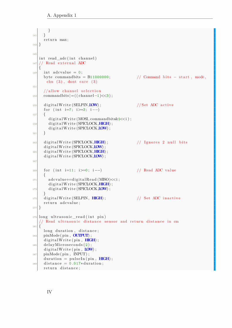
A. Appendix 1
141
return max ;143
145
i n t read_adc ( i n t channel )147 // Read e x t e r n a l ADC
149 i n t adcvalue = 0 ;
byte commandbits = B11000000 ; // Command b i t s − s ta r t , mode ,chn (3 ) , dont care (3 )
151
// a l low channel s e l e c t i o n153 commandbits |=(( channel−1 )<<3 ) ;
155 d i g i t a l W r i t e (SELPIN ,LOW) ; // Set ADC a c t i v ef o r ( i n t i=7 ; i>=3 ; i−−)
157 d i g i t a l W r i t e (MOSI, commandbits&1<<i ) ;
159 d i g i t a l W r i t e (SPICLOCK,HIGH) ;d i g i t a l W r i t e (SPICLOCK,LOW) ;
161
163 d i g i t a l W r i t e (SPICLOCK,HIGH) ; // Ignore s 2 n u l l b i t sd i g i t a l W r i t e (SPICLOCK,LOW) ;
165 d i g i t a l W r i t e (SPICLOCK,HIGH) ;d i g i t a l W r i t e (SPICLOCK,LOW) ;
167
169 f o r ( i n t i=11 ; i>=0 ; i−−) // Read ADC value
171 adcvalue+=dig i ta lRead (MISO)<<i ;d i g i t a l W r i t e (SPICLOCK,HIGH) ;
173 d i g i t a l W r i t e (SPICLOCK,LOW) ;
175 d i g i t a l W r i t e (SELPIN , HIGH) ; // Set ADC i n a c t i v ere turn adcvalue ;
177
179 long u l t ra son i c_read ( i n t pin )// Read u l t r a s o n i c d i s t anc e s enso r and return d i s t anc e in cm
181 long duration , d i s t ance ;
183 pinMode ( pin , OUTPUT) ;d i g i t a l W r i t e ( pin , HIGH) ;
185 delayMicroseconds ( 2 ) ;d i g i t a l W r i t e ( pin , LOW) ;
187 pinMode ( pin , INPUT) ;durat ion = pu l s e In ( pin , HIGH) ;
189 d i s t ance = 0.017∗ durat ion ;r e turn d i s t anc e ;
IV
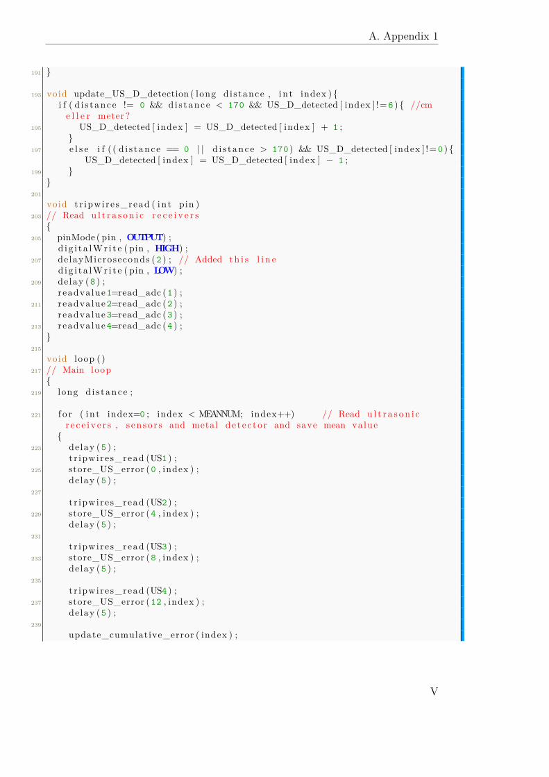
A. Appendix 1
191
193 void update_US_D_detection ( long d i s tance , i n t index ) i f ( d i s t ance != 0 && di s t anc e < 170 && US_D_detected [ index ] != 6 ) //cm
e l l e r meter ?195 US_D_detected [ index ] = US_D_detected [ index ] + 1 ;
197 e l s e i f ( ( d i s t anc e == 0 | | d i s t anc e > 170 ) && US_D_detected [ index ] != 0 )
US_D_detected [ index ] = US_D_detected [ index ] − 1 ;199
201
void t r ipwi re s_read ( i n t pin )203 // Read u l t r a s o n i c r e c e i v e r s
205 pinMode ( pin , OUTPUT) ;
d i g i t a l W r i t e ( pin , HIGH) ;207 delayMicroseconds ( 2 ) ; // Added t h i s l i n e
d i g i t a l W r i t e ( pin , LOW) ;209 delay ( 8 ) ;
readva lue 1=read_adc ( 1 ) ;211 readva lue 2=read_adc ( 2 ) ;
readva lue 3=read_adc ( 3 ) ;213 readva lue 4=read_adc ( 4 ) ;
215
void loop ( )217 // Main loop
219 long d i s t ance ;
221 f o r ( i n t index=0 ; index < MEANNUM; index++) // Read u l t r a s o n i cr e c e i v e r s , s e n s o r s and metal d e t e c t o r and save mean value
223 delay ( 5 ) ;
t r ipwi re s_read (US1 ) ;225 store_US_error ( 0 , index ) ;
de lay ( 5 ) ;227
t r ipwi re s_read (US2 ) ;229 store_US_error ( 4 , index ) ;
de lay ( 5 ) ;231
t r ipwi re s_read (US3 ) ;233 store_US_error ( 8 , index ) ;
de lay ( 5 ) ;235
t r ipwi re s_read (US4 ) ;237 store_US_error ( 12 , index ) ;
de lay ( 5 ) ;239
update_cumulative_error ( index ) ;
V
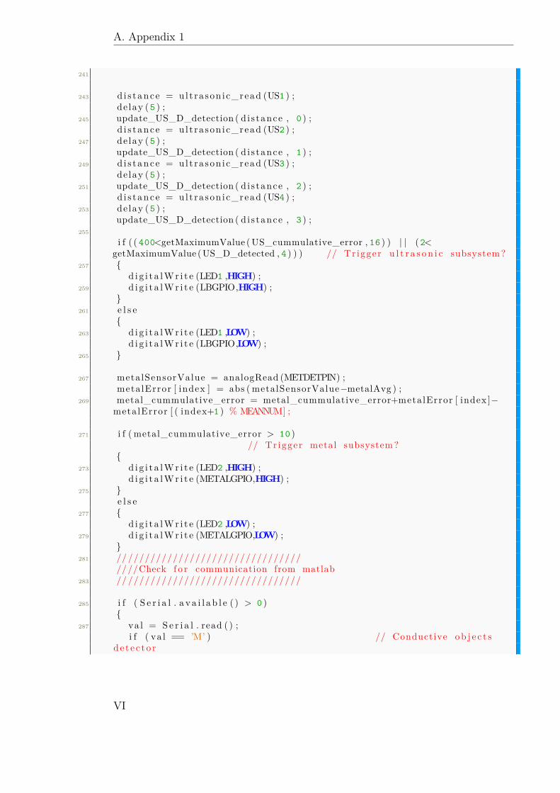
A. Appendix 1
241
243 d i s t ance = ul t ra son i c_read (US1 ) ;de lay ( 5 ) ;
245 update_US_D_detection ( d i s tance , 0 ) ;d i s t ance = ul t ra son i c_read (US2 ) ;
247 delay ( 5 ) ;update_US_D_detection ( d i s tance , 1 ) ;
249 d i s t ance = ul t ra son i c_read (US3 ) ;de lay ( 5 ) ;
251 update_US_D_detection ( d i s tance , 2 ) ;d i s t ance = ul t ra son i c_read (US4 ) ;
253 delay ( 5 ) ;update_US_D_detection ( d i s tance , 3 ) ;
255
i f ( ( 400<getMaximumValue ( US_cummulative_error , 16 ) ) | | ( 2<getMaximumValue ( US_D_detected , 4 ) ) ) // Tr igger u l t r a s o n i c subsystem ?
257 d i g i t a l W r i t e (LED1 ,HIGH) ;
259 d i g i t a l W r i t e (LBGPIO,HIGH) ;
261 e l s e
263 d i g i t a l W r i t e (LED1 ,LOW) ;d i g i t a l W r i t e (LBGPIO,LOW) ;
265
267 metalSensorValue = analogRead (METDETPIN) ;metalError [ index ] = abs ( metalSensorValue−metalAvg ) ;
269 metal_cummulative_error = metal_cummulative_error+metalError [ index ]−metalError [ ( index+1 ) % MEANNUM] ;
271 i f ( metal_cummulative_error > 10 )// Tr igger metal subsystem ?
273 d i g i t a l W r i t e (LED2 ,HIGH) ;
d i g i t a l W r i t e (METALGPIO,HIGH) ;275
e l s e277
d i g i t a l W r i t e (LED2 ,LOW) ;279 d i g i t a l W r i t e (METALGPIO,LOW) ;
281 // ///////////////////////////////
////Check f o r communication from matlab283 // ///////////////////////////////
285 i f ( S e r i a l . a v a i l a b l e ( ) > 0 )
287 va l = S e r i a l . read ( ) ;i f ( va l == ’M’ ) // Conductive o b j e c t s
de t e c t o r
VI
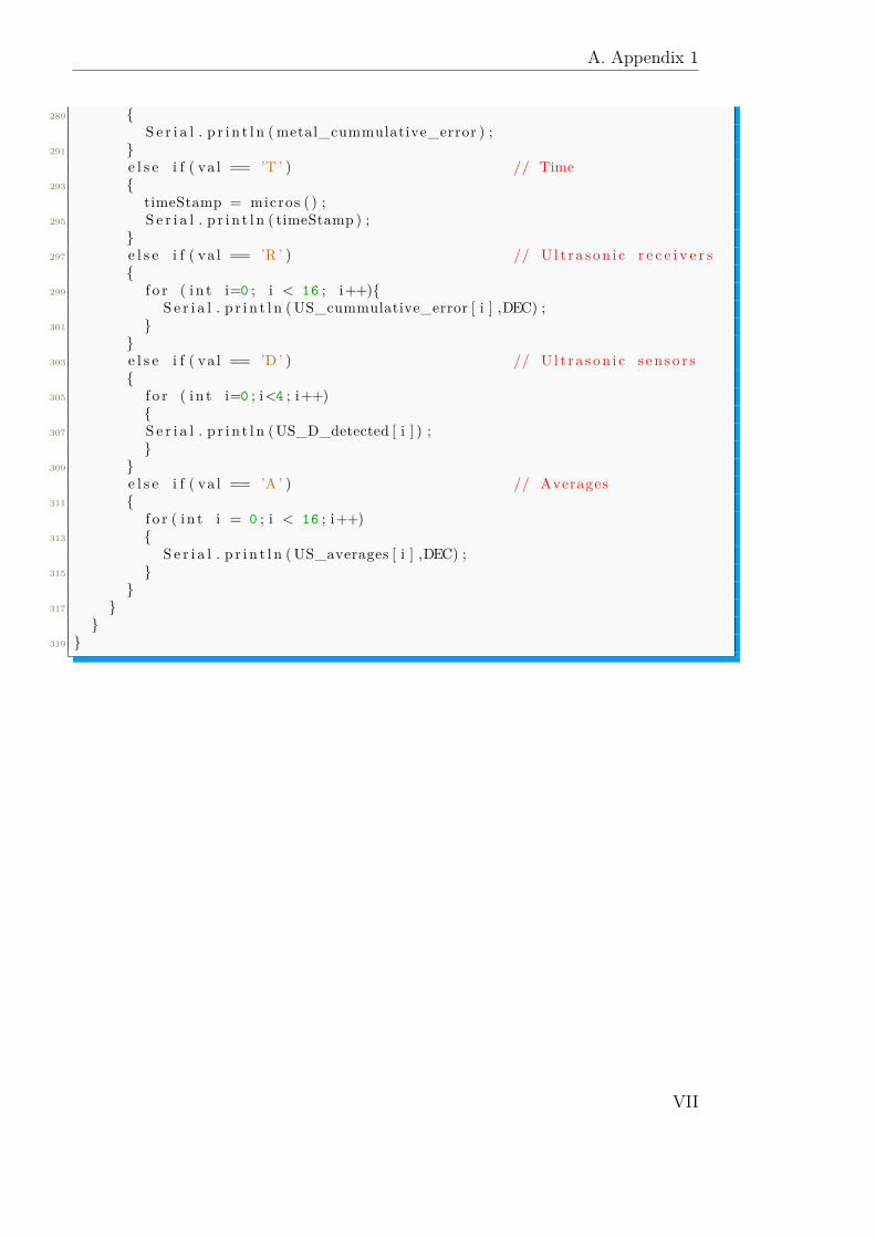
A. Appendix 1
289 S e r i a l . p r i n t l n ( metal_cummulative_error ) ;
291 e l s e i f ( va l == ’T ’ ) // Time
293 timeStamp = micros ( ) ;
295 S e r i a l . p r i n t l n ( timeStamp ) ;
297 e l s e i f ( va l == ’R ’ ) // U l t r a son i c r e c e i v e r s
299 f o r ( i n t i=0 ; i < 16 ; i++)S e r i a l . p r i n t l n ( US_cummulative_error [ i ] ,DEC) ;
301
303 e l s e i f ( va l == ’D’ ) // U l t r a son i c s en s o r s
305 f o r ( i n t i=0 ; i<4 ; i++)
307 S e r i a l . p r i n t l n ( US_D_detected [ i ] ) ;
309 e l s e i f ( va l == ’A ’ ) // Averages
311 f o r ( i n t i = 0 ; i < 16 ; i++)
313 S e r i a l . p r i n t l n ( US_averages [ i ] ,DEC) ;
315
317
319
VII