Embed Size (px)
Citation preview
Renesas Electronics America Inc.
© 2012 Renesas Electronics America Inc. All rights reserved.
Class ID:
Designing with External Flash Memory on Renesas Platforms
Douglas Crane, Segment Manager
Micron Technology
CL23A
© 2012 Renesas Electronics America Inc. All rights reserved. 2
Douglas Crane
Doug is a 27 year veteran in the electronics field. He currently works for Micron Technology as a Sr. Segment Manager driving application strategies, enabling the memory sub-system ecosystem and identifying roadmap requirements for embedded solutions group. Doug has been in the memory business for 16 years, 6 of which is with Micron and 10 with Toshiba in technical marketing roles for memory products. Prior to his memory experience, he spent 11 years involved in systems engineering at McDonnell Douglas and Rockwell. Doug has a BS in Applied Physics from University of California Irvine, MSEE from Cal State Fullerton, and an MBA from the University of Southern California. Doug has been involved in memory standards committee of JEDEC as well as been in the JEDEC board of directors
© 2012 Renesas Electronics America Inc. All rights reserved. 3
Renesas Technology & Solution Portfolio
© 2012 Renesas Electronics America Inc. All rights reserved. 4
Agenda
Market Trends
System Considerations
Flash Cell Architectures
RX62N PCM Demo
Flash Memory Choices
Summary
© 2012 Renesas Electronics America Inc. All rights reserved. 5
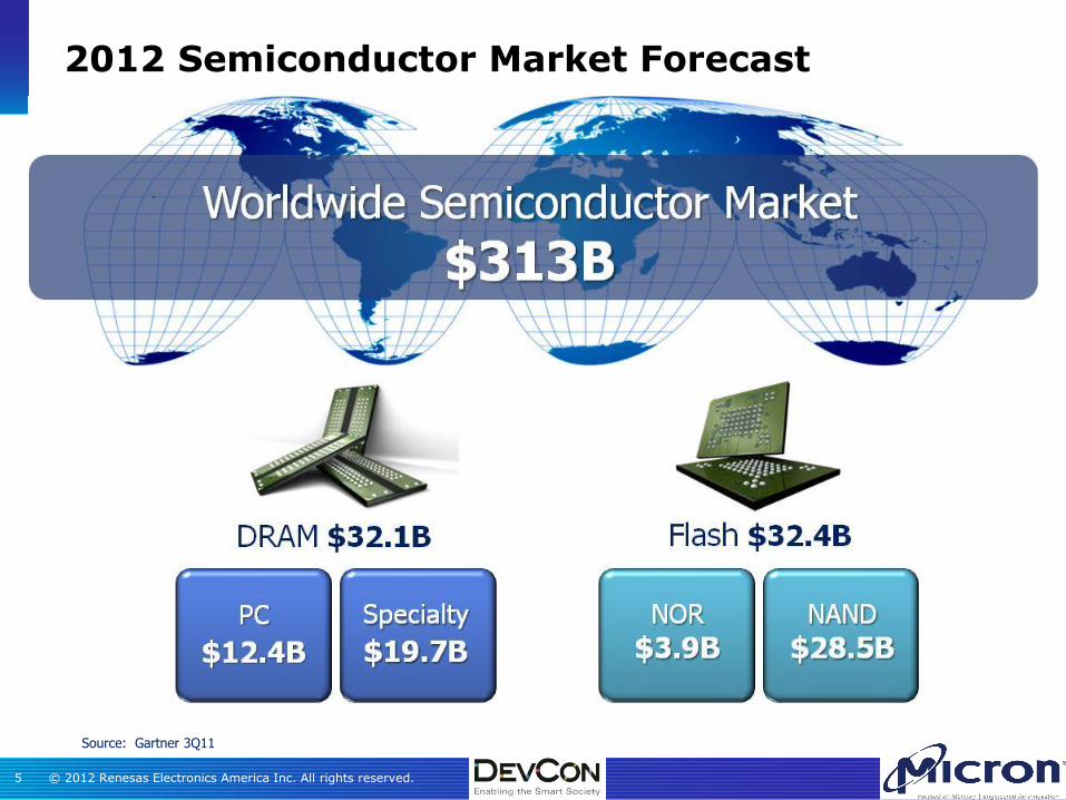
Source: Gartner 3Q11
2012 Semiconductor Market Forecast
© 2012 Renesas Electronics America Inc. All rights reserved. 6
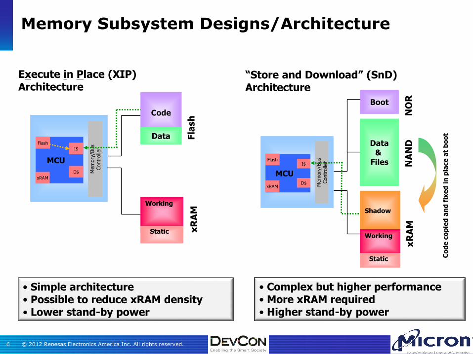
Memory Subsystem Designs/Architecture
Execute in Place (XIP) Architecture
“Store and Download” (SnD) Architecture
• Simple architecture • Possible to reduce xRAM density • Lower stand-by power
• Complex but higher performance • More xRAM required • Higher stand-by power
MCU
Mem
ory
/Bus
Contr
olle
r I$
D$
Code
Data Fla
sh
x
RA
M
Working
Working
Static
Boot
Data &
Files NA
ND
x
RA
M
Working
Static
Shadow
Co
de
co
pie
d a
nd
fix
ed
in
pla
ce
at
bo
ot
NO
R
MCU
Mem
ory
/Bus
Contr
olle
r
I$
D$
Flash
xRAM
Flash
xRAM

© 2012 Renesas Electronics America Inc. All rights reserved. 7
Platform Internal Flash
External Flash Memory
SNOR PNOR Managed
NAND
x32
RH850 256K-8MB
V850 16KB-2MB
RX 32K-2MB 128Mb
SuperH
SH2/2A 16K-2MB
SH4/4A X
H8SX 128K-1MB
X8/ x16
RL78 2KB-512KB 8Mb
SoC R Car H1 X eMMC
R Car M1x X eMMC
Platform Memory Mapping
© 2012 Renesas Electronics America Inc. All rights reserved. 8
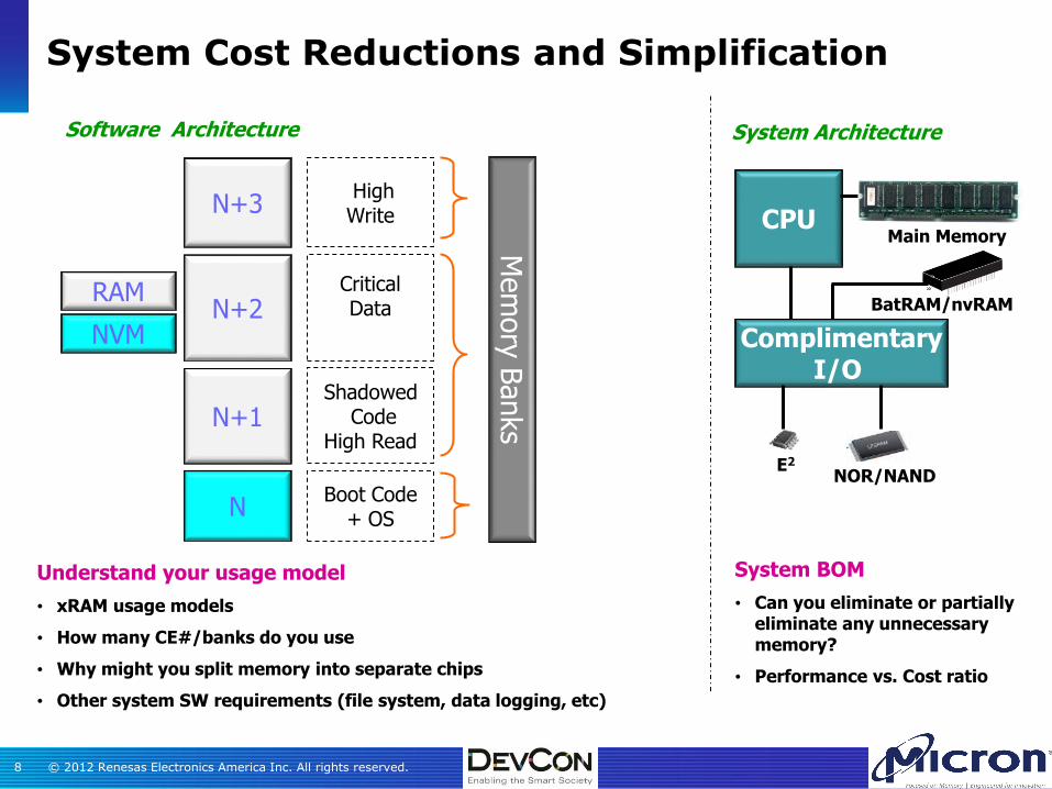
System Cost Reductions and Simplification
Understand your usage model
• xRAM usage models
• How many CE#/banks do you use
• Why might you split memory into separate chips
• Other system SW requirements (file system, data logging, etc)
Software Architecture
System BOM
• Can you eliminate or partially eliminate any unnecessary memory?
• Performance vs. Cost ratio
System Architecture
N+1
N
NVM
RAM
Boot Code + OS
Shadowed Code
High Read
N+2 Critical
Data
N+3 High Write
Mem
ory
Banks
Complimentary I/O
CPU Main Memory
E2
NOR/NAND
BatRAM/nvRAM
© 2012 Renesas Electronics America Inc. All rights reserved. 9
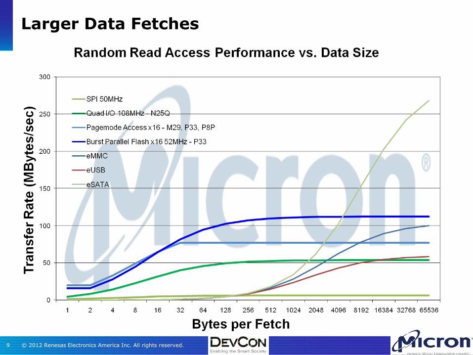
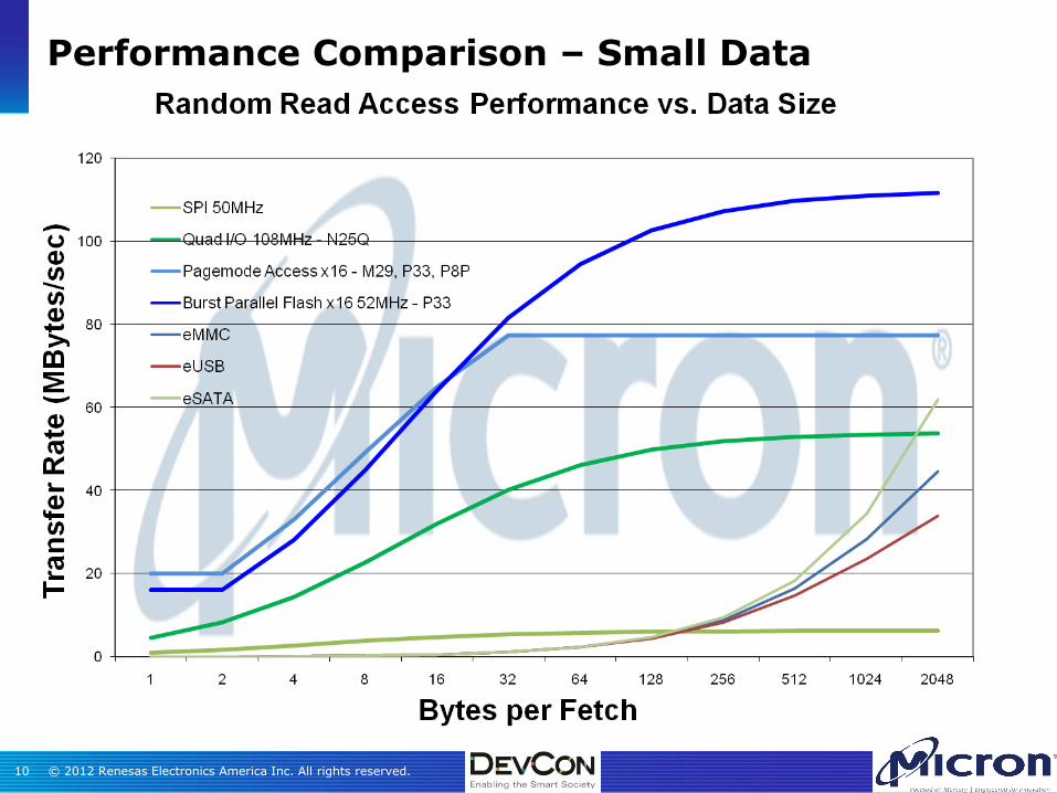
Larger Data Fetches
© 2012 Renesas Electronics America Inc. All rights reserved. 10
Performance Comparison – Small Data
© 2012 Renesas Electronics America Inc. All rights reserved. 11
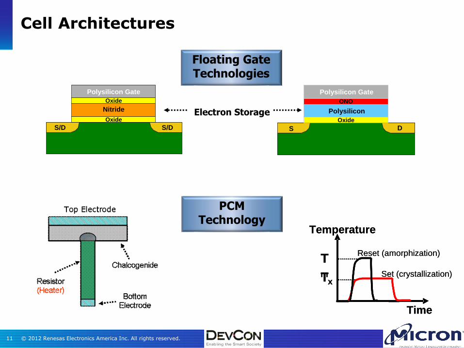
Cell Architectures
Floating Gate Technologies
S/D S/D
Polysilicon Gate
Oxide
Nitride
Oxide
S D
Polysilicon Gate
Oxide
ONO
Polysilicon
PCM Technology
Time
Temperature
Tx
Tm
Reset (amorphization)
Set (crystallization)
Time
Temperature
Tx
Tm
Reset (amorphization)
Set (crystallization)
Electron Storage
© 2012 Renesas Electronics America Inc. All rights reserved. 12
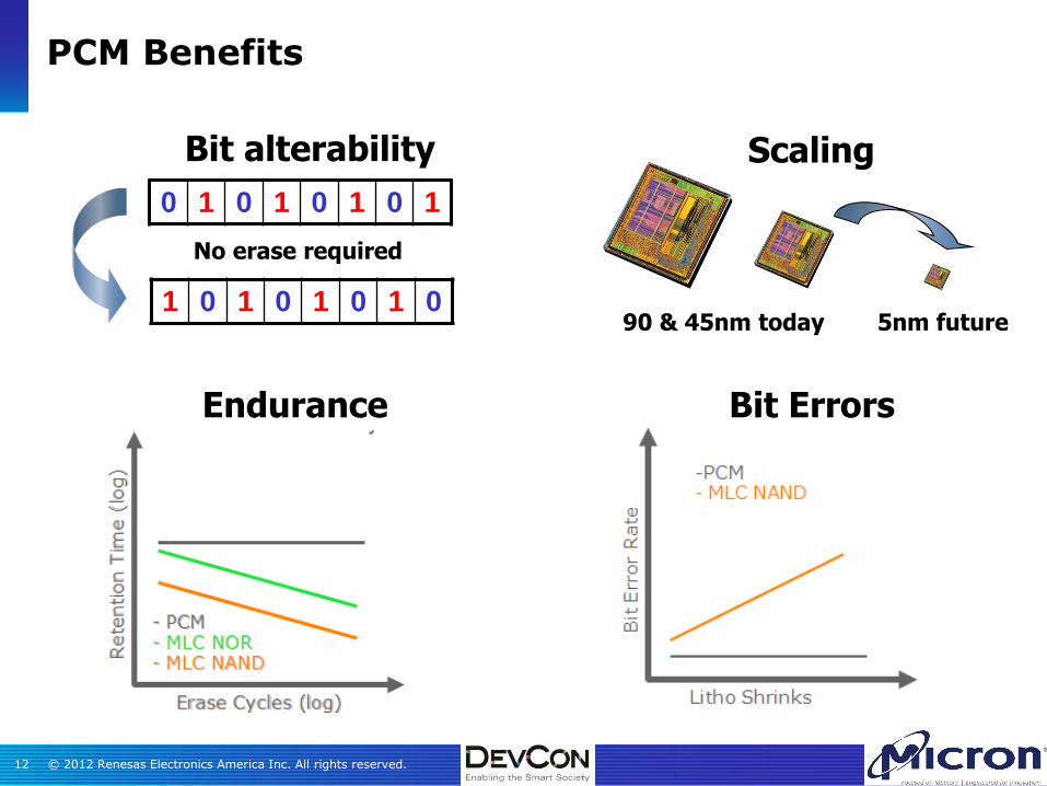
PCM Benefits
Bit Errors Endurance
Bit alterability Scaling
90 & 45nm today 5nm future
0 1 0 1 0 1 0 1
1 0 1 0 1 0 1 0
No erase required
© 2012 Renesas Electronics America Inc. All rights reserved. 13
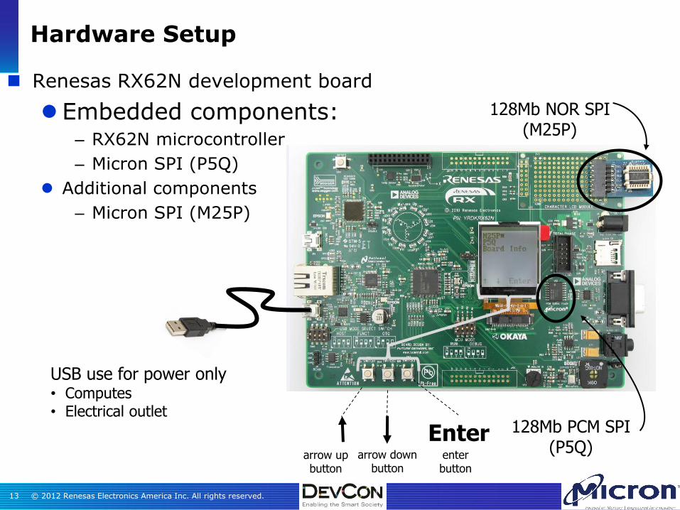
Renesas RX62N development board
Embedded components: – RX62N microcontroller
– Micron SPI (P5Q)
Additional components
– Micron SPI (M25P)
Hardware Setup
Enter arrow up button
arrow down button
enter button
128Mb NOR SPI (M25P)
128Mb PCM SPI (P5Q)
USB use for power only • Computes • Electrical outlet
© 2012 Renesas Electronics America Inc. All rights reserved. 14
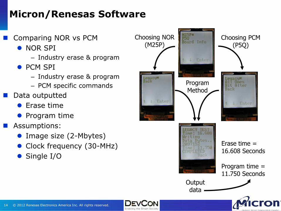
Comparing NOR vs PCM
NOR SPI
– Industry erase & program
PCM SPI
– Industry erase & program
– PCM specific commands
Data outputted
Erase time
Program time
Assumptions:
Image size (2-Mbytes)
Clock frequency (30-MHz)
Single I/O
Micron/Renesas Software
Choosing NOR (M25P)
Choosing PCM (P5Q)
Program Method
Erase time = 16.608 Seconds
Program time = 11.750 Seconds
Output data
© 2012 Renesas Electronics America Inc. All rights reserved. 15
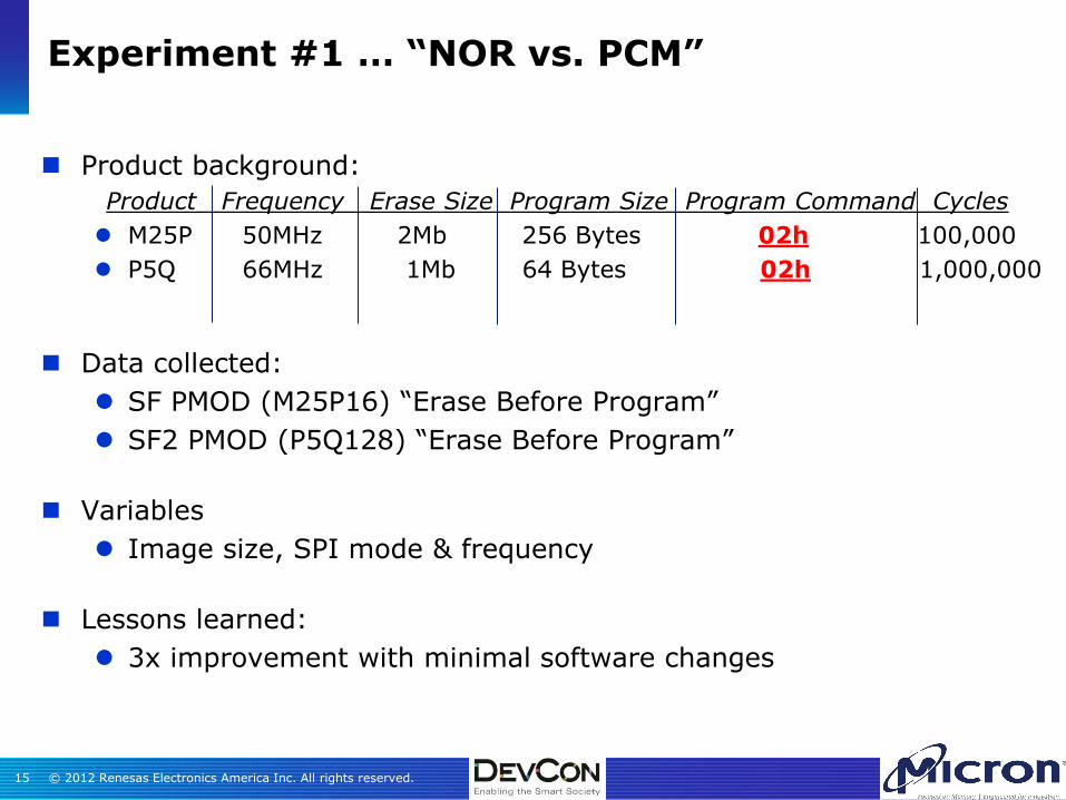
Product background:
Product Frequency Erase Size Program Size Program Command Cycles
M25P 50MHz 2Mb 256 Bytes 02h 100,000
P5Q 66MHz 1Mb 64 Bytes 02h 1,000,000
Data collected:
SF PMOD (M25P16) “Erase Before Program”
SF2 PMOD (P5Q128) “Erase Before Program”
Variables
Image size, SPI mode & frequency
Lessons learned:
3x improvement with minimal software changes
Experiment #1 … “NOR vs. PCM”
© 2012 Renesas Electronics America Inc. All rights reserved. 16
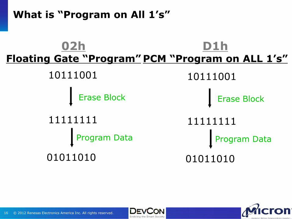
What is “Program on All 1’s”
02h Floating Gate “Program”
D1h PCM “Program on ALL 1’s”
10111001
11111111
01011010
Erase Block
Program Data
10111001
11111111
01011010
Erase Block
Program Data
© 2012 Renesas Electronics America Inc. All rights reserved. 17
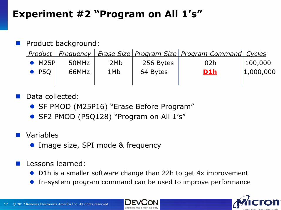
Product background:
Product Frequency Erase Size Program Size Program Command Cycles
M25P 50MHz 2Mb 256 Bytes 02h 100,000
P5Q 66MHz 1Mb 64 Bytes D1h 1,000,000
Data collected:
SF PMOD (M25P16) “Erase Before Program”
SF2 PMOD (P5Q128) “Program on All 1’s”
Variables
Image size, SPI mode & frequency
Lessons learned:
D1h is a smaller software change than 22h to get 4x improvement
In-system program command can be used to improve performance
Experiment #2 “Program on All 1’s”
© 2012 Renesas Electronics America Inc. All rights reserved. 18
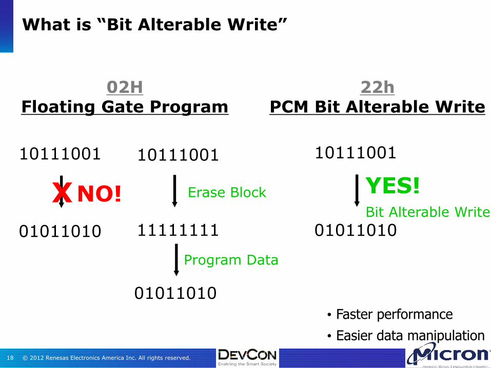
What is “Bit Alterable Write”
02H Floating Gate Program
22h PCM Bit Alterable Write
10111001
01011010
10111001 10111001
01011010
YES! X
11111111
01011010
NO! Erase Block
Program Data
• Faster performance
• Easier data manipulation
Bit Alterable Write
© 2012 Renesas Electronics America Inc. All rights reserved. 19
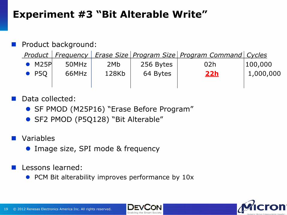
Product background:
Product Frequency Erase Size Program Size Program Command Cycles
M25P 50MHz 2Mb 256 Bytes 02h 100,000
P5Q 66MHz 128Kb 64 Bytes 22h 1,000,000
Data collected:
SF PMOD (M25P16) “Erase Before Program”
SF2 PMOD (P5Q128) “Bit Alterable”
Variables
Image size, SPI mode & frequency
Lessons learned:
PCM Bit alterability improves performance by 10x
Experiment #3 “Bit Alterable Write”
© 2012 Renesas Electronics America Inc. All rights reserved. 20
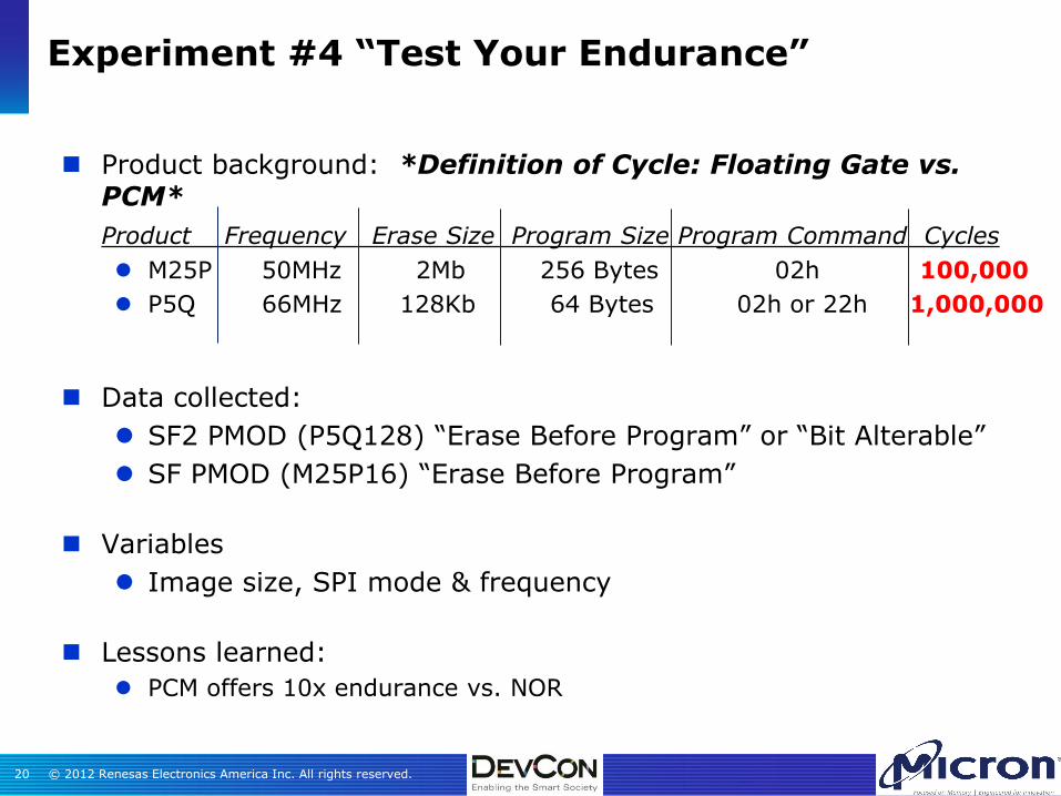
Product background: *Definition of Cycle: Floating Gate vs. PCM*
Product Frequency Erase Size Program Size Program Command Cycles
M25P 50MHz 2Mb 256 Bytes 02h 100,000
P5Q 66MHz 128Kb 64 Bytes 02h or 22h 1,000,000
Data collected:
SF2 PMOD (P5Q128) “Erase Before Program” or “Bit Alterable”
SF PMOD (M25P16) “Erase Before Program”
Variables
Image size, SPI mode & frequency
Lessons learned:
PCM offers 10x endurance vs. NOR
Experiment #4 “Test Your Endurance”
© 2012 Renesas Electronics America Inc. All rights reserved. 21
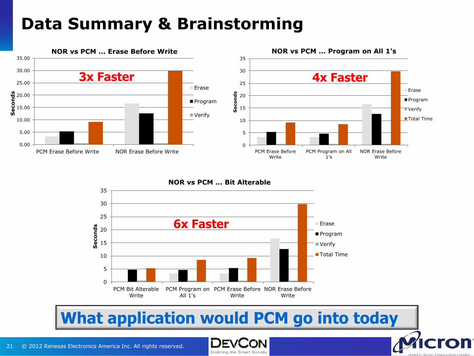
What application would PCM go into today
0.00
5.00
10.00
15.00
20.00
25.00
30.00
35.00
PCM Erase Before Write NOR Erase Before Write
Seco
nd
s
NOR vs PCM ... Erase Before Write
Erase
Program
Verify
0
5
10
15
20
25
30
35
PCM Erase Before
Write
PCM Program on All
1's
NOR Erase Before
Write
Seco
nd
s
NOR vs PCM ... Program on All 1's
Erase
Program
Verify
Total Time
0
5
10
15
20
25
30
35
PCM Bit AlterableWrite
PCM Program onAll 1's
PCM Erase BeforeWrite
NOR Erase BeforeWrite
Seco
nd
s
NOR vs PCM ... Bit Alterable
Erase
Program
Verify
Total Time
Data Summary & Brainstorming
3x Faster 4x Faster
6x Faster
© 2012 Renesas Electronics America Inc. All rights reserved. 22
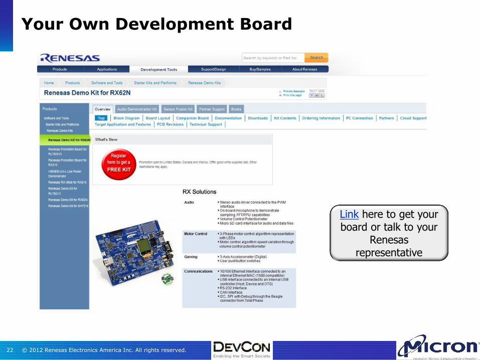
Your Own Development Board
Link here to get your board or talk to your
Renesas representative
© 2012 Renesas Electronics America Inc. All rights reserved. 23
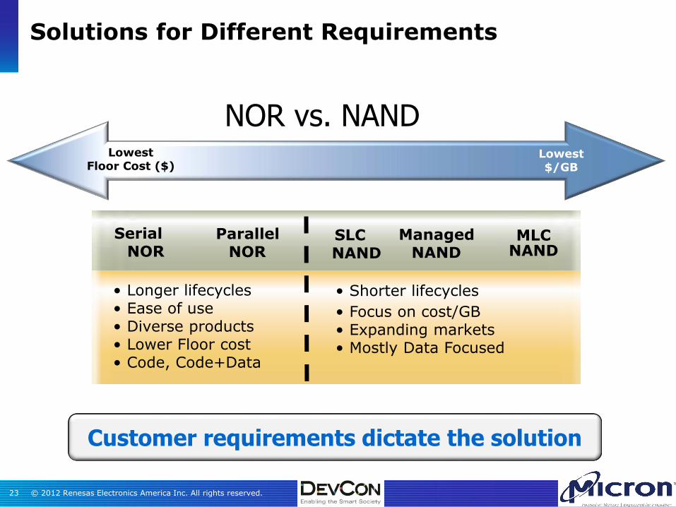
Solutions for Different Requirements
• Shorter lifecycles
• Focus on cost/GB • Expanding markets • Mostly Data Focused
• Longer lifecycles • Ease of use • Diverse products • Lower Floor cost • Code, Code+Data
Lowest Floor Cost ($)
Lowest $/GB
Serial NOR
Parallel NOR
SLC NAND
Managed NAND
MLC NAND
NOR vs. NAND
Customer requirements dictate the solution
© 2012 Renesas Electronics America Inc. All rights reserved. 24
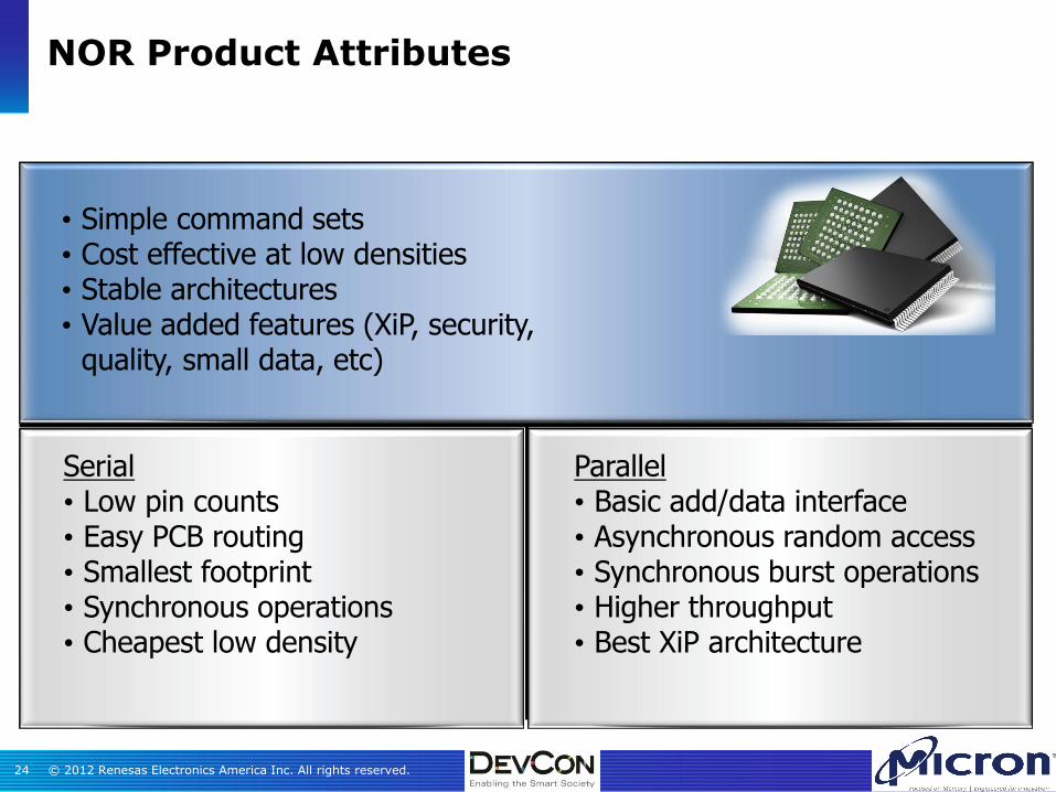
NOR Product Attributes
• Simple command sets • Cost effective at low densities • Stable architectures • Value added features (XiP, security,
quality, small data, etc)
Serial • Low pin counts • Easy PCB routing • Smallest footprint • Synchronous operations • Cheapest low density
Parallel • Basic add/data interface • Asynchronous random access • Synchronous burst operations • Higher throughput • Best XiP architecture
© 2012 Renesas Electronics America Inc. All rights reserved. 25
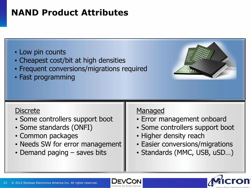
NAND Product Attributes
• Low pin counts • Cheapest cost/bit at high densities • Frequent conversions/migrations required • Fast programming
Discrete • Some controllers support boot • Some standards (ONFI) • Common packages • Needs SW for error management • Demand paging – saves bits
Managed • Error management onboard • Some controllers support boot • Higher density reach • Easier conversions/migrations • Standards (MMC, USB, uSD…)
© 2012 Renesas Electronics America Inc. All rights reserved. 26
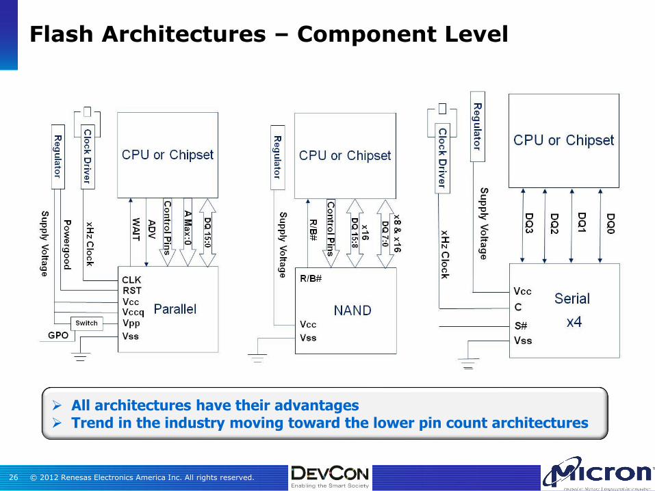
Flash Architectures – Component Level
All architectures have their advantages Trend in the industry moving toward the lower pin count architectures
© 2012 Renesas Electronics America Inc. All rights reserved. 27
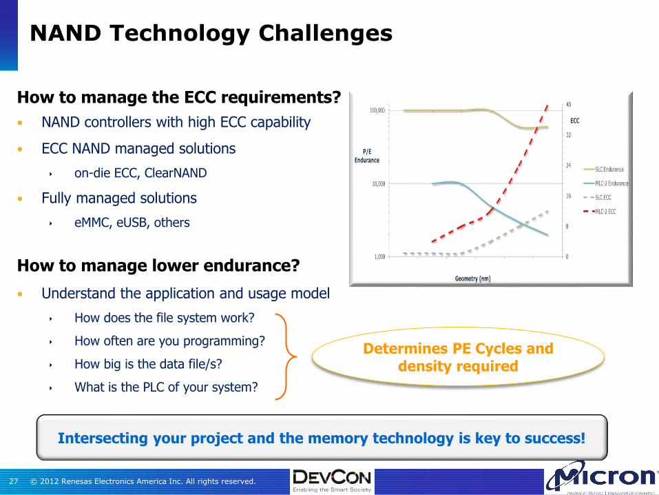
NAND Technology Challenges
How to manage the ECC requirements?
• NAND controllers with high ECC capability
• ECC NAND managed solutions
on-die ECC, ClearNAND
• Fully managed solutions
eMMC, eUSB, others
How to manage lower endurance?
• Understand the application and usage model
How does the file system work?
How often are you programming?
How big is the data file/s?
What is the PLC of your system?
Intersecting your project and the memory technology is key to success!
Determines PE Cycles and density required
© 2012 Renesas Electronics America Inc. All rights reserved. 28
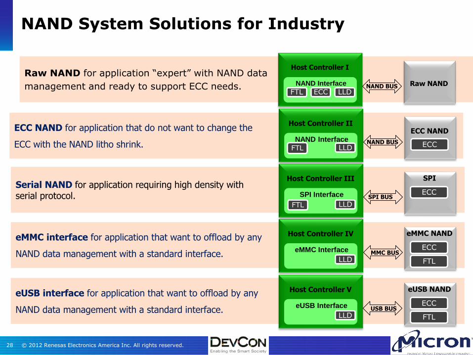
eMMC interface for application that want to offload by any
NAND data management with a standard interface.
Serial NAND for application requiring high density with serial protocol.
ECC NAND for application that do not want to change the
ECC with the NAND litho shrink.
Raw NAND for application “expert” with NAND data
management and ready to support ECC needs.
NAND System Solutions for Industry
Raw NAND
Host Controller I
NAND Interface
LLD ECC FTL NAND BUS
ECC NAND Host Controller II
NAND Interface LLD FTL
NAND BUS ECC
eMMC NAND
ECC
FTL
Host Controller IV
eMMC Interface
LLD MMC BUS
SPI
ECC
Host Controller III
SPI Interface
LLD SPI BUS
FTL
eUSB interface for application that want to offload by any
NAND data management with a standard interface.
eUSB NAND
ECC
FTL
Host Controller V
eUSB Interface
LLD USB BUS
© 2012 Renesas Electronics America Inc. All rights reserved. 29
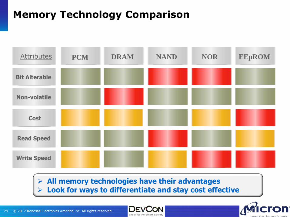
Memory Technology Comparison
Attributes
Bit Alterable
Non-volatile
Cost
Read Speed
Write Speed
DRAM NAND NOR EEpROM PCM
All memory technologies have their advantages Look for ways to differentiate and stay cost effective
© 2012 Renesas Electronics America Inc. All rights reserved. 30
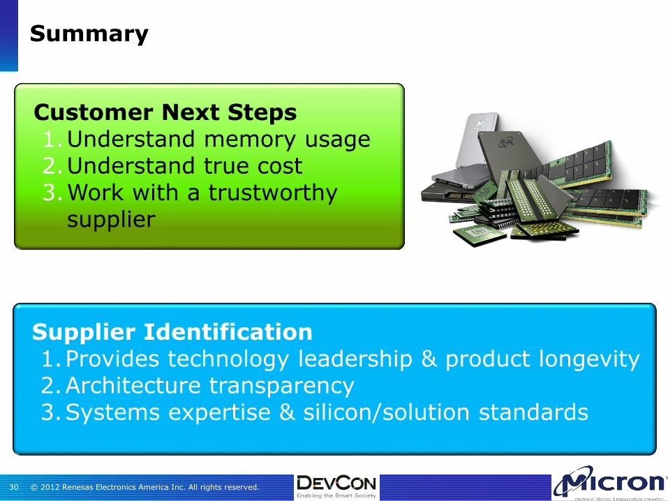
Customer Next Steps 1.Understand memory usage 2.Understand true cost 3.Work with a trustworthy
supplier
Summary
Supplier Identification 1.Provides technology leadership & product longevity 2.Architecture transparency 3.Systems expertise & silicon/solution standards
© 2012 Renesas Electronics America Inc. All rights reserved. 31
Questions?

© 2012 Renesas Electronics America Inc. All rights reserved. 32
Please Provide Your Feedback…
Please utilize the ‘Guidebook’ application to leave feedback
or
Ask me for the paper feedback form for you to use…
Renesas Electronics America Inc.
© 2012 Renesas Electronics America Inc. All rights reserved.
Class ID: