Embed Size (px)
Citation preview
ETRI Journal, Volume 33, Number 3, June 2011 © 2011 Antonio Lopez Martin et al. 393
A systematic approach for the design of two-stage class AB CMOS unity-gain buffers is proposed. It is based on the inclusion of a class AB operation to class A Miller amplifier topologies in unity-gain negative feedback by a simple technique that does not modify quiescent currents, supply requirements, noise performance, or static power. Three design examples are fabricated in a 0.5 μm CMOS process. Measurement results show slew rate improvement factors of approximately 100 for the class AB buffers versus their class A counterparts for the same quiescent power consumption (< 200 μW).
Keywords: Analog integrated circuits, CMOS buffer, CMOS voltage follower, quasi-floating gate.
Manuscript received Aug. 3, 2010; revised Oct. 5, 2010; accepted Oct. 25, 2010. This work was supported by the Spanish Dirección General de Investigación and FEDER
funds under grant TEC2010-21563-C02. Antonio Lopez Martin (phone: +34948169311, email: [email protected]) and Jose
Maria Algueta Miguel (email: [email protected]) are with the Department of Electrical and Electronic Engineering, Public University of Navarra, Navarra, Spain.
Lucia Acosta (email: [email protected]) and Ramón Gonzalez Carvajal (email: [email protected]) are with the Department of Electrical and Computer Engineering, University of Seville, Seville, Spain.
Jaime Ramírez-Angulo (email: [email protected]) is with the Department of Electrical and Computer Engineering, New Mexico State University, Las Cruces, New Mexico, USA.
doi:10.4218/etrij.11.0110.0465
I. Introduction
Class AB buffers are required in low-power analog design and mixed-signal design to drive low impedance loads. In these scenarios, adequate dynamic performance must be compatible with low quiescent power consumption. This requirement is not viable if buffers operate in class A since, in this case, the load current is limited by the quiescent current of the output stage, leading to a tradeoff between slew rate and quiescent power. Class AB implementations solve this design constraint by providing dynamic currents to the load which are not limited by the quiescent currents. Several class AB buffers have been proposed which are mainly based on using a properly biased push-pull output stage [1]-[5]. However, typical shortcomings of these proposals are that the additional circuitry employed to get class AB operation often increases power consumption, decreases current efficiency (defined as the percentage of supply current that is delivered to the load), and sometimes does not feature accurate control of quiescent currents. Another typical shortcoming of some buffers is that there is a DC level shift between the input and the output voltage [6], [7], which is often dependent on temperature and process variations and that can be important if the buffer is used in a single-ended configuration.
In this paper, we propose a technique to systematically derive two-stage class AB unity-gain buffers from class A implementations. The technique is based on the use of quasi-floating gate (QFG) techniques [8]-[11] which allow the inclusion of a class AB operation without requiring additional power consumption or supply voltage and featuring a simple and accurate control of quiescent currents.
The paper is organized as follows. Section II describes the
Design of Two-Stage Class AB CMOS Buffers: A Systematic Approach
Antonio Lopez Martin, Jose Maria Algueta Miguel, Lucia Acosta, Jaime Ramírez-Angulo, and Ramón Gonzalez Carvajal
394 Antonio Lopez Martin et al. ETRI Journal, Volume 33, Number 3, June 2011
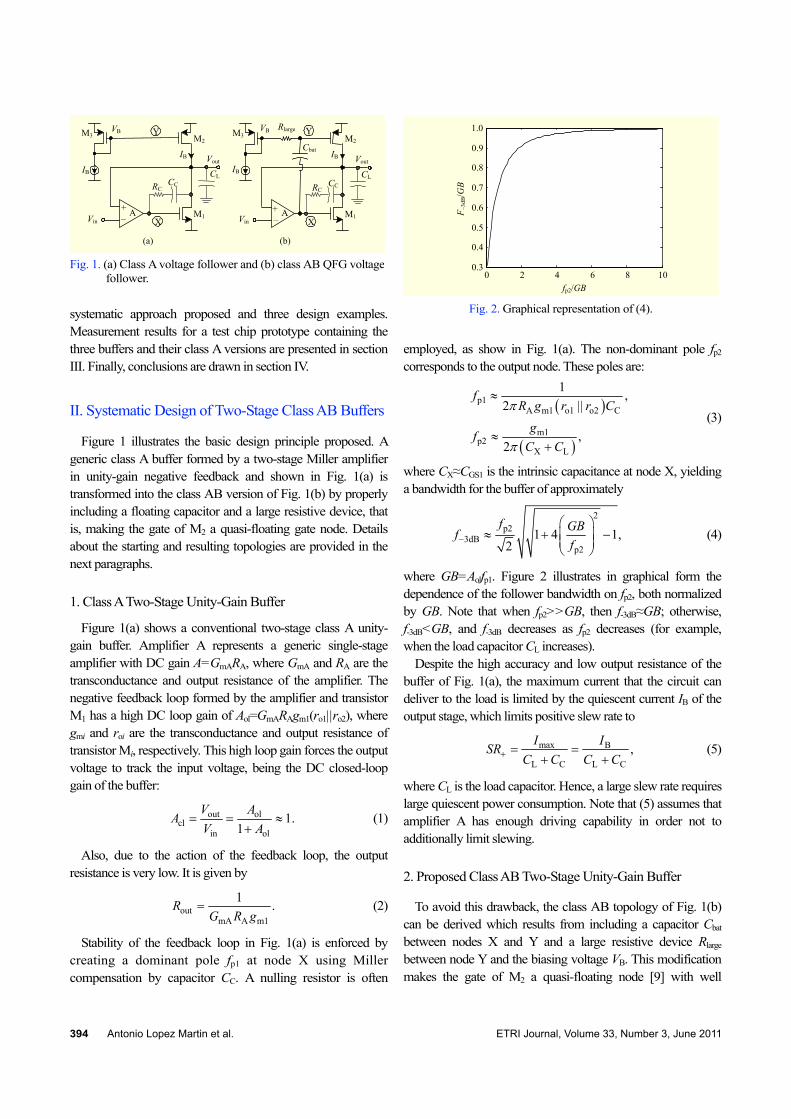
Fig. 1. (a) Class A voltage follower and (b) class AB QFG voltagefollower.
IB Vout
M1
M2 M3
IB
+ –
A Vin
RC CC IB
M1
M2M3
IB
+ –
A Vin
RC CC
Cbat
VB VB Rlarge
X
Y
X
Y
CL Vout
CL
(a) (b)
systematic approach proposed and three design examples. Measurement results for a test chip prototype containing the three buffers and their class A versions are presented in section III. Finally, conclusions are drawn in section IV.
II. Systematic Design of Two-Stage Class AB Buffers
Figure 1 illustrates the basic design principle proposed. A generic class A buffer formed by a two-stage Miller amplifier in unity-gain negative feedback and shown in Fig. 1(a) is transformed into the class AB version of Fig. 1(b) by properly including a floating capacitor and a large resistive device, that is, making the gate of M2 a quasi-floating gate node. Details about the starting and resulting topologies are provided in the next paragraphs.
1. Class A Two-Stage Unity-Gain Buffer
Figure 1(a) shows a conventional two-stage class A unity-gain buffer. Amplifier A represents a generic single-stage amplifier with DC gain A=GmARA, where GmA and RA are the transconductance and output resistance of the amplifier. The negative feedback loop formed by the amplifier and transistor M1 has a high DC loop gain of Aol=GmARAgm1(ro1||ro2), where gmi and roi are the transconductance and output resistance of transistor Mi, respectively. This high loop gain forces the output voltage to track the input voltage, being the DC closed-loop gain of the buffer:
out olcl
in ol1.
1V A
AV A
= = ≈+
(1)
Also, due to the action of the feedback loop, the output resistance is very low. It is given by
outmA A m1
1 .RG R g
= (2)
Stability of the feedback loop in Fig. 1(a) is enforced by creating a dominant pole fp1 at node X using Miller compensation by capacitor CC. A nulling resistor is often
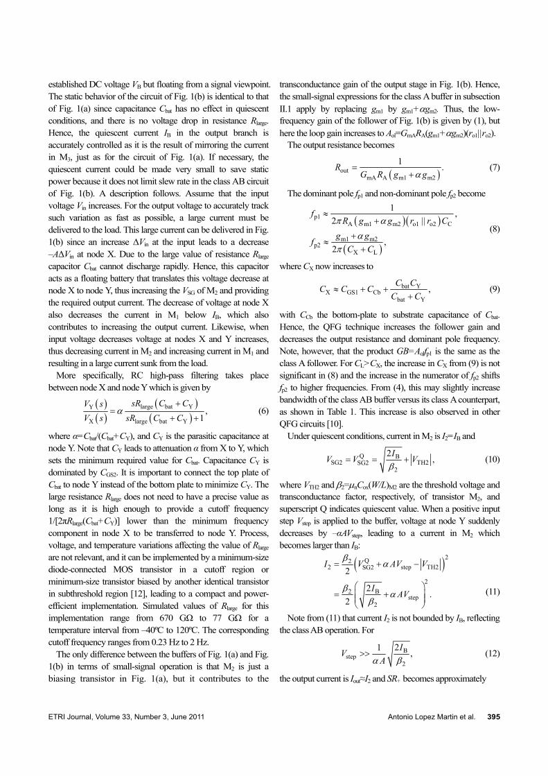
Fig. 2. Graphical representation of (4).
0 2 4 6 8 100.3
0.4
0.5
0.6
0.7
0.8
0.9
1.0
fp2/GB
F –3d
B/G
B
employed, as show in Fig. 1(a). The non-dominant pole fp2 corresponds to the output node. These poles are:
( )
( )
p1A m1 o1 o2 C
m1p2
X L
1 ,2 ||
,2
fR g r r C
gfC C
π
π
≈
≈+
(3)
where CX≈CGS1 is the intrinsic capacitance at node X, yielding a bandwidth for the buffer of approximately
2p2
3dBp2
1 4 1,2
f GBff−
⎛ ⎞≈ + −⎜ ⎟⎜ ⎟
⎝ ⎠ (4)
where GB=Aolfp1. Figure 2 illustrates in graphical form the dependence of the follower bandwidth on fp2, both normalized by GB. Note that when fp2>>GB, then f-3dB≈GB; otherwise, f-3dB<GB, and f-3dB decreases as fp2 decreases (for example, when the load capacitor CL increases).
Despite the high accuracy and low output resistance of the buffer of Fig. 1(a), the maximum current that the circuit can deliver to the load is limited by the quiescent current IB of the output stage, which limits positive slew rate to
max B
L C L C,
I ISR
C C C C+ = =+ +
(5)
where CL is the load capacitor. Hence, a large slew rate requires large quiescent power consumption. Note that (5) assumes that amplifier A has enough driving capability in order not to additionally limit slewing.
2. Proposed Class AB Two-Stage Unity-Gain Buffer
To avoid this drawback, the class AB topology of Fig. 1(b) can be derived which results from including a capacitor Cbat between nodes X and Y and a large resistive device Rlarge between node Y and the biasing voltage VB. This modification makes the gate of M2 a quasi-floating node [9] with well
ETRI Journal, Volume 33, Number 3, June 2011 Antonio Lopez Martin et al. 395
established DC voltage VB but floating from a signal viewpoint. The static behavior of the circuit of Fig. 1(b) is identical to that of Fig. 1(a) since capacitance Cbat has no effect in quiescent conditions, and there is no voltage drop in resistance Rlarge. Hence, the quiescent current IB in the output branch is accurately controlled as it is the result of mirroring the current in M3, just as for the circuit of Fig. 1(a). If necessary, the quiescent current could be made very small to save static power because it does not limit slew rate in the class AB circuit of Fig. 1(b). A description follows. Assume that the input voltage Vin increases. For the output voltage to accurately track such variation as fast as possible, a large current must be delivered to the load. This large current can be delivered in Fig. 1(b) since an increase ΔVin at the input leads to a decrease –AΔVin at node X. Due to the large value of resistance Rlarge capacitor Cbat cannot discharge rapidly. Hence, this capacitor acts as a floating battery that translates this voltage decrease at node X to node Y, thus increasing the VSG of M2 and providing the required output current. The decrease of voltage at node X also decreases the current in M1 below IB, which also contributes to increasing the output current. Likewise, when input voltage decreases voltage at nodes X and Y increases, thus decreasing current in M2 and increasing current in M1 and resulting in a large current sunk from the load.
More specifically, RC high-pass filtering takes place between node X and node Y which is given by
( )( )
( )( )
large bat YY
X large bat Y,
1sR C CV s
V s sR C Cα
+=
+ + (6)
where α=Cbat/(Cbat+CY), and CY is the parasitic capacitance at node Y. Note that CY leads to attenuation α from X to Y, which sets the minimum required value for Cbat. Capacitance CY is dominated by CGS2. It is important to connect the top plate of Cbat to node Y instead of the bottom plate to minimize CY. The large resistance Rlarge does not need to have a precise value as long as it is high enough to provide a cutoff frequency 1/[2πRlarge(Cbat+CY)] lower than the minimum frequency component in node X to be transferred to node Y. Process, voltage, and temperature variations affecting the value of Rlarge are not relevant, and it can be implemented by a minimum-size diode-connected MOS transistor in a cutoff region or minimum-size transistor biased by another identical transistor in subthreshold region [12], leading to a compact and power-efficient implementation. Simulated values of Rlarge for this implementation range from 670 GΩ to 77 GΩ for a temperature interval from –40ºC to 120ºC. The corresponding cutoff frequency ranges from 0.23 Hz to 2 Hz.
The only difference between the buffers of Fig. 1(a) and Fig. 1(b) in terms of small-signal operation is that M2 is just a biasing transistor in Fig. 1(a), but it contributes to the
transconductance gain of the output stage in Fig. 1(b). Hence, the small-signal expressions for the class A buffer in subsection II.1 apply by replacing gm1 by gm1+αgm2. Thus, the low-frequency gain of the follower of Fig. 1(b) is given by (1), but here the loop gain increases to Aol=GmARA(gm1+αgm2)(ro1||ro2).
The output resistance becomes
( )outmA A m1 m2
1 .RG R g gα
=+
(7)
The dominant pole fp1 and non-dominant pole fp2 become
( ) ( )
( )
p1A m1 m2 o1 o2 C
m1 m2p2
X L
1 ,2 ||
,2
fR g g r r C
g gfC C
π α
απ
≈+
+≈
+
(8)
where CX now increases to
bat YX GS1 Cb
bat Y,
C CC C C
C C≈ + +
+ (9)
with CCb the bottom-plate to substrate capacitance of Cbat. Hence, the QFG technique increases the follower gain and decreases the output resistance and dominant pole frequency. Note, however, that the product GB=Aolfp1 is the same as the class A follower. For CL>CX, the increase in CX from (9) is not significant in (8) and the increase in the numerator of fp2 shifts fp2 to higher frequencies. From (4), this may slightly increase bandwidth of the class AB buffer versus its class A counterpart, as shown in Table 1. This increase is also observed in other QFG circuits [10].
Under quiescent conditions, current in M2 is I2=IB and
Q BSG2 TH2SG2
2
2,
IV V V
β= = + (10)
where VTH2 and β2=μnCox(W/L)M2 are the threshold voltage and transconductance factor, respectively, of transistor M2, and superscript Q indicates quiescent value. When a positive input step Vstep is applied to the buffer, voltage at node Y suddenly decreases by –αAVstep, leading to a current in M2 which becomes larger than IB:
( )2Q22 step TH2SG2
22 B
step2
2
2.
2
I V AV V
IAV
βα
βα
β
= + −
⎛ ⎞= +⎜ ⎟⎜ ⎟
⎝ ⎠
(11)
Note from (11) that current I2 is not bounded by IB, reflecting the class AB operation. For
Bstep
2
21 ,I
VAα β
>> (12)
the output current is Iout≈I2 and SR+ becomes approximately
396 Antonio Lopez Martin et al. ETRI Journal, Volume 33, Number 3, June 2011
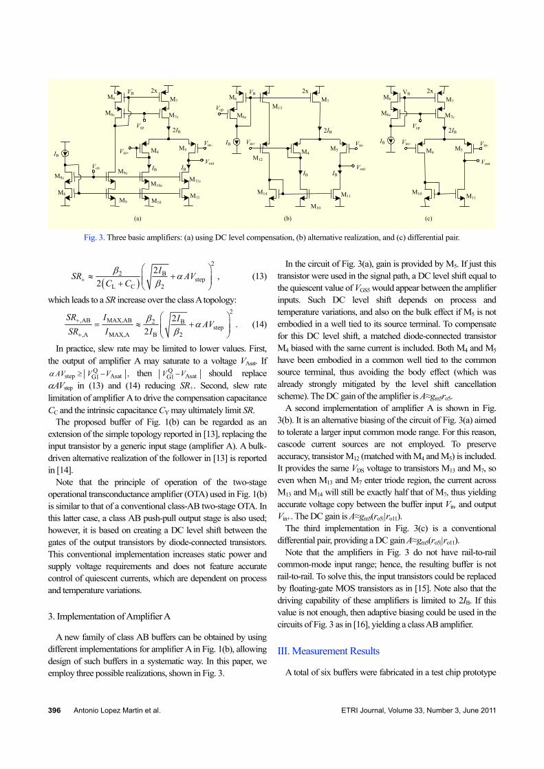
Fig. 3. Three basic amplifiers: (a) using DC level compensation, (b) alternative realization, and (c) differential pair.
M7 M6
M7c M6c
Vcp
M8
IB
Vcn M8c
M4 M5
2IB
Vin+ Vin-
IB IB Vout
M9
M9c
M10
M10c
M11
M11c
2x VB M7
M6
M6c
Vcp
IB
M4M5
2IB
Vin-
IB IB
Vout
M11
2xVB
Vin+
M14
M10
M7M6
M7cM6c
Vcp
M4 M5
2IB
Vin+ Vin-
Vout
M10 M11
2x VB
M12
M13
IB
(a) (b) (c)
( )
22 B
stepL C 2
2,
2I
SR AVC C
βα
β+
⎛ ⎞≈ +⎜ ⎟⎜ ⎟+ ⎝ ⎠
(13)
which leads to a SR increase over the class A topology: 2
,AB MAX,AB 2 Bstep
,A MAX,A B 2
2.
2SR I I
AVSR I I
βα
β+
+
⎛ ⎞= ≈ +⎜ ⎟⎜ ⎟
⎝ ⎠ (14)
In practice, slew rate may be limited to lower values. First, the output of amplifier A may saturate to a voltage VAsat. If
Qstep AsatG1 ,AV V Vα ≥ − then Q
AsatG1V V− should replace αAVstep in (13) and (14) reducing SR+. Second, slew rate limitation of amplifier A to drive the compensation capacitance CC and the intrinsic capacitance CY may ultimately limit SR.
The proposed buffer of Fig. 1(b) can be regarded as an extension of the simple topology reported in [13], replacing the input transistor by a generic input stage (amplifier A). A bulk-driven alternative realization of the follower in [13] is reported in [14].
Note that the principle of operation of the two-stage operational transconductance amplifier (OTA) used in Fig. 1(b) is similar to that of a conventional class-AB two-stage OTA. In this latter case, a class AB push-pull output stage is also used; however, it is based on creating a DC level shift between the gates of the output transistors by diode-connected transistors. This conventional implementation increases static power and supply voltage requirements and does not feature accurate control of quiescent currents, which are dependent on process and temperature variations.
3. Implementation of Amplifier A
A new family of class AB buffers can be obtained by using different implementations for amplifier A in Fig. 1(b), allowing design of such buffers in a systematic way. In this paper, we employ three possible realizations, shown in Fig. 3.
In the circuit of Fig. 3(a), gain is provided by M5. If just this transistor were used in the signal path, a DC level shift equal to the quiescent value of VGS5 would appear between the amplifier inputs. Such DC level shift depends on process and temperature variations, and also on the bulk effect if M5 is not embodied in a well tied to its source terminal. To compensate for this DC level shift, a matched diode-connected transistor M4 biased with the same current is included. Both M4 and M5 have been embodied in a common well tied to the common source terminal, thus avoiding the body effect (which was already strongly mitigated by the level shift cancellation scheme). The DC gain of the amplifier is A≈gm5ro5.
A second implementation of amplifier A is shown in Fig. 3(b). It is an alternative biasing of the circuit of Fig. 3(a) aimed to tolerate a larger input common mode range. For this reason, cascode current sources are not employed. To preserve accuracy, transistor M12 (matched with M4 and M5) is included. It provides the same VDS voltage to transistors M13 and M7, so even when M13 and M7 enter triode region, the current across M13 and M14 will still be exactly half that of M7, thus yielding accurate voltage copy between the buffer input Vin- and output Vin+. The DC gain is A≈gm5(ro5||ro11).
The third implementation in Fig. 3(c) is a conventional differential pair, providing a DC gain A≈gm5(ro5||ro11).
Note that the amplifiers in Fig. 3 do not have rail-to-rail common-mode input range; hence, the resulting buffer is not rail-to-rail. To solve this, the input transistors could be replaced by floating-gate MOS transistors as in [15]. Note also that the driving capability of these amplifiers is limited to 2IB. If this value is not enough, then adaptive biasing could be used in the circuits of Fig. 3 as in [16], yielding a class AB amplifier.
III. Measurement Results
A total of six buffers were fabricated in a test chip prototype
ETRI Journal, Volume 33, Number 3, June 2011 Antonio Lopez Martin et al. 397
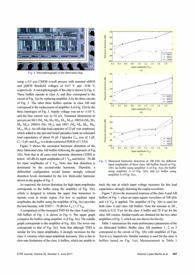
Fig. 4. Microphotograph of the fabricated chip.
AB buffer #3 AB buffer #2 AB buffer #1
using a 0.5 μm CMOS n-well process with nominal nMOS and pMOS threshold voltages of 0.67 V and –0.96 V, respectively. A microphotograph of the chip is shown in Fig. 4. Three buffers operate in class A, and they correspond to the circuit of Fig. 1(a) by replacing amplifier A by the three circuits of Fig. 3. The other three buffers operate in class AB and correspond to the replacement of amplifier A in Fig. 1(b) by the three topologies of Fig. 3. Supply voltage was set to ±1.65 V, and the bias current was IB=10 μA. Transistor dimensions in μm/μm are 60/1 (M1, M8, M9, M10, M11, M14), 100/0.6 (M2, M3, M6, M6c), 200/0.6 (M7, M7c), and 100/1 (M4, M5, M8c, M9c, M11c, M12). An off-chip load capacitor of 22 pF was employed, which added to the pad and board parasitics leads an estimated load capacitance of about 30 pF. Capacitor Cbat was of 1 pF, CC=2 pF, and Rlarge is a diode-connected PMOS of 1.5/0.6.
Figure 5 shows the measured harmonic distortion of the three fabricated class AB buffers following the approach of Fig. 1(b). Note that in all cases total harmonic distortion (THD) is below –60 dB for input amplitudes of 1 Vpp and below –50 dB for input amplitudes of 2 Vpp. Note also that distortion is dominated by the second-order harmonic. Therefore, a differential configuration would feature strongly reduced distortion levels dominated by the low third-order harmonic shown in the graphs of Fig. 5.
As expected, the lowest distortion for high input amplitudes corresponds to the buffer using the amplifier of Fig. 3(b), which is designed to tolerate the upper bias transistors to operate even in triode region. For low to medium input amplitudes, the buffer using the amplifier of Fig. 3(c) provides the best linearity, with THD < –70 dB for Vin ≤ 1.5 Vpp.
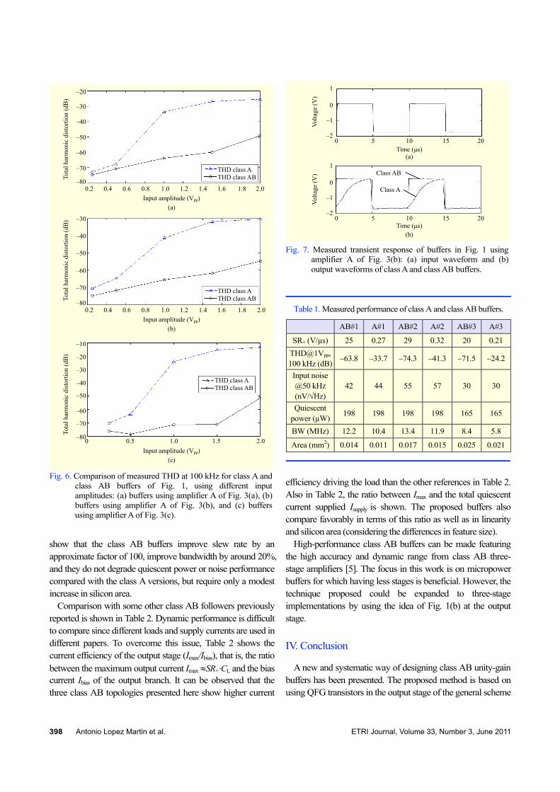
A comparison of the measured THD for the class A and class AB buffers of Fig. 1 is shown in Fig. 6. The upper graph compares the buffers using amplifier A of Fig. 3(a). The middle graph corresponds to the amplifier of Fig. 3(b). The lower one corresponds to that of Fig. 3(c). Note that although THD is similar for low input amplitudes, it strongly increases for the class A versions when input amplitude increases. This is due to slew-rate limitations of the class A buffers, which are unable to
Fig. 5. Measured harmonic distortion at 100 kHz for differentinput amplitudes of three class AB buffers based on Fig.1(b): (a) buffer using amplifier A of Fig. 3(a), (b) bufferusing amplifier A of Fig. 3(b), and (c) buffer usingamplifier A of Fig. 3(c).
0.2 0.4 0.6 0.8 1.0 1.2 1.4 1.6 1.8Input amplitude (Vpp)
–50
–60
–70
–80
–90
–100
Har
mon
ic d
isto
rtion
(dB
)
HD2HD3THD
(a)
0.2 0.4 0.6 0.8 1.0 1.2 1.4 1.6 1.8Input amplitude (Vpp)
–50
–60
–70
–80
–90H
arm
onic
dis
torti
on (d
B)
HD2HD3THD
(b)
0.2 0.4 0.6 0.8 1.0 1.2 1.4 1.6 1.8Input amplitude (Vpp)
Har
mon
ic d
isto
rtion
(dB
)
HD2HD3THD
(c)
–50
–60
–70
–80
–90
–100
track the rate at which input voltage increases for this load capacitance, strongly distorting the output waveform.
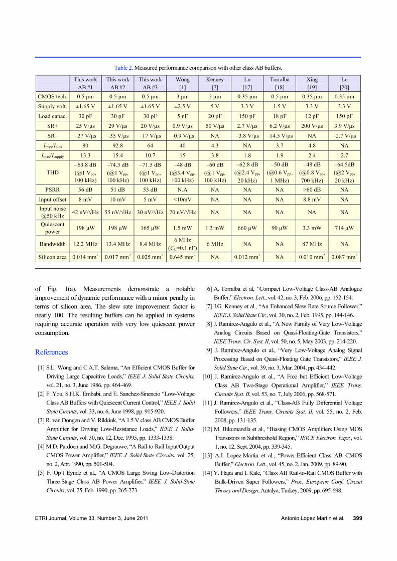
Figure 7 shows the measured response of the class A and AB buffers of Fig. 1 when an input square waveform of 100 kHz and 1.8 Vpp is applied. The amplifier of Fig. 3(b) is used for both class A and class AB buffers. Note the increase in SR+, which is 0.32 V/μs for the class A buffer and 29 V/μs for the class AB version. Similar results are obtained for the two other amplifiers of Fig. 3, which are not shown for brevity.
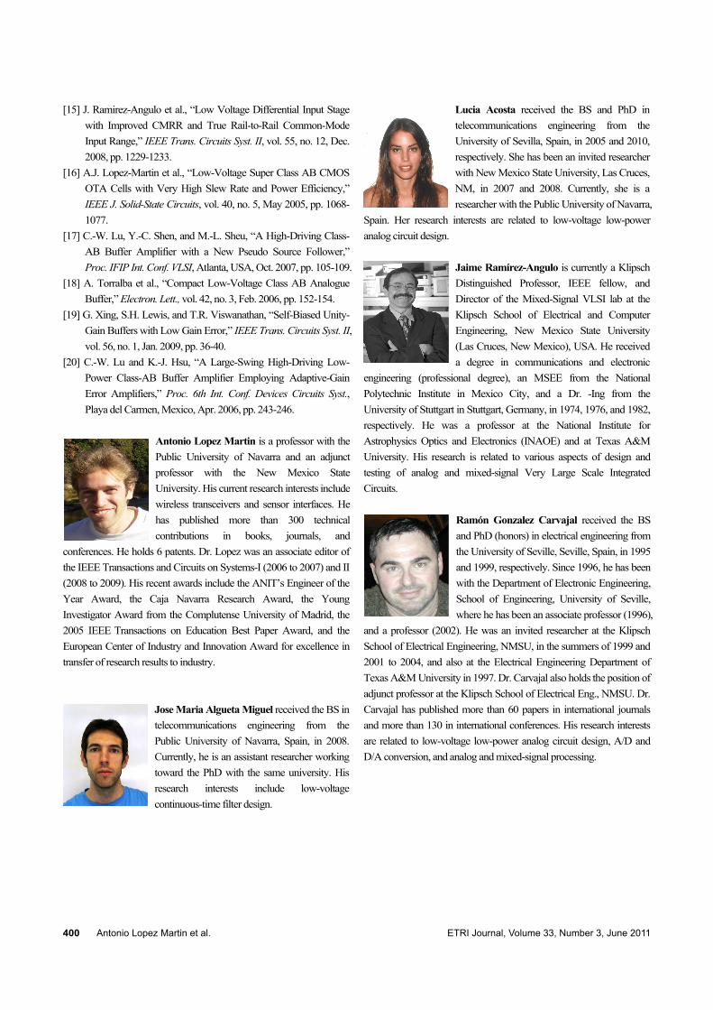
Table 1 summarizes the main performance parameters of the six fabricated buffers. Buffer class AB numbers 1, 2, or 3 correspond to the circuit of Fig. 1(b) with amplifier of Figs. 3(a) to (c), respectively. Similar notation is used for the class A buffers based on Fig. 1(a). Measurements in Table 1
398 Antonio Lopez Martin et al. ETRI Journal, Volume 33, Number 3, June 2011
THD class A
Fig. 6. Comparison of measured THD at 100 kHz for class A andclass AB buffers of Fig. 1, using different inputamplitudes: (a) buffers using amplifier A of Fig. 3(a), (b)buffers using amplifier A of Fig. 3(b), and (c) buffersusing amplifier A of Fig. 3(c).
0.2 0.4 0.6 0.8 1.0 1.2 1.4 1.6 1.8Input amplitude (Vpp)
–30
–40
–50
–60
–70
–80Tota
l har
mon
ic d
isto
rtion
(dB
)
THD class ATHD class AB
(a)
–20
0.2 0.4 0.6 0.8 1.0 1.2 1.4 1.6 1.8Input amplitude (Vpp)
–30
–40
–50
–60
–70
–80Tota
l har
mon
ic d
isto
rtion
(dB
)
THD class ATHD class AB
(b)
0 0.5 1.0 1.5 2.0Input amplitude (Vpp)
(c)
–30
–40
–50
–60
–70
–80Tota
l har
mon
ic d
isto
rtion
(dB
) –20
–10
THD class ATHD class AB
2.0
2.0
show that the class AB buffers improve slew rate by an approximate factor of 100, improve bandwidth by around 20%, and they do not degrade quiescent power or noise performance compared with the class A versions, but require only a modest increase in silicon area.
Comparison with some other class AB followers previously reported is shown in Table 2. Dynamic performance is difficult to compare since different loads and supply currents are used in different papers. To overcome this issue, Table 2 shows the current efficiency of the output stage (Imax/Ibias), that is, the ratio between the maximum output current Imax ≈SR+·CL and the bias current Ibias of the output branch. It can be observed that the three class AB topologies presented here show higher current
Fig. 7. Measured transient response of buffers in Fig. 1 usingamplifier A of Fig. 3(b): (a) input waveform and (b)output waveforms of class A and class AB buffers.
0 5 10 15 20
(a)
0 5 10 15 20
(b) Time (µs)
1
0
–1
–2
Volta
ge (V
)
1
0
–1
–2
Volta
ge (V
) Class AB
Class A
Time (µs)
Table 1. Measured performance of class A and class AB buffers.
AB#1 A#1 AB#2 A#2 AB#3 A#3
SR+ (V/µs) 25 0.27 29 0.32 20 0.21THD@1Vpp, 100 kHz (dB) –63.8 –33.7 –74.3 –41.3 –71.5 –24.2
Input noise @50 kHz (nV/√Hz)
42 44 55 57 30 30
Quiescent power (µW) 198 198 198 198 165 165
BW (MHz) 12.2 10.4 13.4 11.9 8.4 5.8
Area (mm2) 0.014 0.011 0.017 0.015 0.025 0.021
efficiency driving the load than the other references in Table 2. Also in Table 2, the ratio between Imax and the total quiescent current supplied Isupply is shown. The proposed buffers also compare favorably in terms of this ratio as well as in linearity and silicon area (considering the differences in feature size).
High-performance class AB buffers can be made featuring the high accuracy and dynamic range from class AB three-stage amplifiers [5]. The focus in this work is on micropower buffers for which having less stages is beneficial. However, the technique proposed could be expanded to three-stage implementations by using the idea of Fig. 1(b) at the output stage.
IV. Conclusion
A new and systematic way of designing class AB unity-gain buffers has been presented. The proposed method is based on using QFG transistors in the output stage of the general scheme
ETRI Journal, Volume 33, Number 3, June 2011 Antonio Lopez Martin et al. 399
Table 2. Measured performance comparison with other class AB buffers.
This work
AB #1 This work
AB #2 This work
AB #3 Wong
[1] Kenney
[7] Lu
[17] Torralba
[18] Xing [19]
Lu [20]
CMOS tech. 0.5 μm 0.5 μm 0.5 μm 3 μm 2 μm 0.35 μm 0.5 μm 0.35 μm 0.35 μm
Supply volt. ±1.65 V ±1.65 V ±1.65 V ±2.5 V 5 V 3.3 V 1.5 V 3.3 V 3.3 V
Load capac. 30 pF 30 pF 30 pF 5 nF 20 pF 150 pF 18 pF 12 pF 150 pF
SR+ 25 V/μs 29 V/μs 20 V/μs 0.9 V/μs 50 V/μs 2.7 V/μs 6.2 V/μs 200 V/μs 3.9 V/μs
SR– –27 V/μs –35 V/μs –17 V/μs –0.9 V/μs NA –3.8 V/μs –14.5 V/μs NA –2.7 V/μs
Imax/Ibias 80 92.8 64 40 4.3 NA 3.7 4.8 NA
Imax/Isupply 13.3 15.4 10.7 15 3.8 1.8 1.9 2.4 2.7
THD –63.8 dB (@1 Vpp, 100 kHz)
–74.3 dB (@1 Vpp, 100 kHz)
–71.5 dB (@1 Vpp, 100 kHz)
–48 dB (@3.4 Vpp, 100 kHz)
–60 dB (@1 Vpp, 100 kHz)
–62.8 dB(@2.4 Vpp,
20 kHz)
–50 dB (@0.6 Vpp,
1 MHz)
–48 dB (@0.8 Vpp, 700 kHz)
–64.5dB(@2 Vpp,20 kHz)
PSRR 56 dB 51 dB 53 dB N.A NA NA NA >60 dB NA Input offset 8 mV 10 mV 5 mV <10mV NA NA NA 8.8 mV NA Input noise @50 kHz 42 nV/√Hz 55 nV/√Hz 30 nV/√Hz 70 nV/√Hz NA NA NA NA NA
Quiescent power 198 μW 198 μW 165 μW 1.5 mW 1.3 mW 660 μW 90 μW 3.3 mW 714 μW
Bandwidth 12.2 MHz 13.4 MHz 8.4 MHz 6 MHz
(CL=0.1 nF)6 MHz NA NA 87 MHz NA
Silicon area 0.014 mm2 0.017 mm2 0.025 mm2 0.645 mm2 NA 0.012 mm2 NA 0.010 mm2 0.087 mm2
of Fig. 1(a). Measurements demonstrate a notable improvement of dynamic performance with a minor penalty in terms of silicon area. The slew rate improvement factor is nearly 100. The resulting buffers can be applied in systems requiring accurate operation with very low quiescent power consumption.
References
[1] S.L. Wong and C.A.T. Salama, “An Efficient CMOS Buffer for Driving Large Capacitive Loads,” IEEE J. Solid State Circuits, vol. 21, no. 3, June 1986, pp. 464-469.
[2] F. You, S.H.K. Embabi, and E. Sanchez-Sinencio “Low-Voltage Class AB Buffers with Quiescent Current Control,” IEEE J. Solid State Circuits, vol. 33, no. 6, June 1998, pp. 915-920.
[3] R. van Dongen and V. Rikkink, “A 1.5 V class AB CMOS Buffer Amplifier for Driving Low-Resistance Loads,” IEEE J. Solid-State Circuits, vol. 30, no. 12, Dec. 1995, pp. 1333-1338.
[4] M.D. Pardoen and M.G. Degrauwe, “A Rail-to-Rail Input/Output CMOS Power Amplifier,” IEEE J. Solid-State Circuits, vol. 25, no. 2, Apr. 1990, pp. 501-504.
[5] F. Op’t Eynde et al., “A CMOS Large Swing Low-Distortion Three-Stage Class AB Power Amplifier,” IEEE J. Solid-State Circuits, vol. 25, Feb. 1990, pp. 265-273.
[6] A. Torralba et al, “Compact Low-Voltage Class-AB Analogue Buffer,” Electron. Lett., vol. 42, no. 3, Feb. 2006, pp. 152-154.
[7] J.G. Kenney et al., “An Enhanced Slew Rate Source Follower,” IEEE J. Solid State Cir., vol. 30, no. 2, Feb. 1995, pp. 144-146.
[8] J. Ramirez-Angulo et al., “A New Family of Very Low-Voltage Analog Circuits Based on Quasi-Floating-Gate Transistors,” IEEE Trans. Cir. Syst. II, vol. 50, no. 5, May 2003, pp. 214-220.
[9] J. Ramirez-Angulo et al., “Very Low-Voltage Analog Signal Processing Based on Quasi-Floating Gate Transistors,” IEEE J. Solid State Cir., vol. 39, no. 3, Mar. 2004, pp. 434-442.
[10] J. Ramirez-Angulo et al., “A Free but Efficient Low-Voltage Class AB Two-Stage Operational Amplifier,” IEEE Trans. Circuits Syst. II, vol. 53, no. 7, July 2006, pp. 568-571.
[11] J. Ramirez-Angulo et al., “Class-AB Fully Differential Voltage Followers,” IEEE Trans. Circuits Syst. II, vol. 55, no. 2, Feb. 2008, pp. 131-135.
[12] M. Bikumandla et al., “Biasing CMOS Amplifiers Using MOS Transistors in Subthreshold Region,” IEICE Electron. Expr., vol. 1, no. 12, Sept. 2004, pp. 339-345.
[13] A.J. Lopez-Martin et al., “Power-Efficient Class AB CMOS Buffer,” Electron. Lett., vol. 45, no. 2, Jan. 2009, pp. 89-90.
[14] Y. Haga and I. Kale, “Class AB Rail-to-Rail CMOS Buffer with Bulk-Driven Super Followers,” Proc. European Conf. Circuit Theory and Design, Antalya, Turkey, 2009, pp. 695-698.
400 Antonio Lopez Martin et al. ETRI Journal, Volume 33, Number 3, June 2011
[15] J. Ramirez-Angulo et al., “Low Voltage Differential Input Stage with Improved CMRR and True Rail-to-Rail Common-Mode Input Range,” IEEE Trans. Circuits Syst. II, vol. 55, no. 12, Dec. 2008, pp. 1229-1233.
[16] A.J. Lopez-Martin et al., “Low-Voltage Super Class AB CMOS OTA Cells with Very High Slew Rate and Power Efficiency,” IEEE J. Solid-State Circuits, vol. 40, no. 5, May 2005, pp. 1068-1077.
[17] C.-W. Lu, Y.-C. Shen, and M.-L. Sheu, “A High-Driving Class-AB Buffer Amplifier with a New Pseudo Source Follower,” Proc. IFIP Int. Conf. VLSI, Atlanta, USA, Oct. 2007, pp. 105-109.
[18] A. Torralba et al., “Compact Low-Voltage Class AB Analogue Buffer,” Electron. Lett., vol. 42, no. 3, Feb. 2006, pp. 152-154.
[19] G. Xing, S.H. Lewis, and T.R. Viswanathan, “Self-Biased Unity-Gain Buffers with Low Gain Error,” IEEE Trans. Circuits Syst. II, vol. 56, no. 1, Jan. 2009, pp. 36-40.
[20] C.-W. Lu and K.-J. Hsu, “A Large-Swing High-Driving Low-Power Class-AB Buffer Amplifier Employing Adaptive-Gain Error Amplifiers,” Proc. 6th Int. Conf. Devices Circuits Syst., Playa del Carmen, Mexico, Apr. 2006, pp. 243-246.
Antonio Lopez Martin is a professor with the Public University of Navarra and an adjunct professor with the New Mexico State University. His current research interests include wireless transceivers and sensor interfaces. He has published more than 300 technical contributions in books, journals, and
conferences. He holds 6 patents. Dr. Lopez was an associate editor of the IEEE Transactions and Circuits on Systems-I (2006 to 2007) and II (2008 to 2009). His recent awards include the ANIT’s Engineer of the Year Award, the Caja Navarra Research Award, the Young Investigator Award from the Complutense University of Madrid, the 2005 IEEE Transactions on Education Best Paper Award, and the European Center of Industry and Innovation Award for excellence in transfer of research results to industry.
Jose Maria Algueta Miguel received the BS in telecommunications engineering from the Public University of Navarra, Spain, in 2008. Currently, he is an assistant researcher working toward the PhD with the same university. His research interests include low-voltage continuous-time filter design.
Lucia Acosta received the BS and PhD in telecommunications engineering from the University of Sevilla, Spain, in 2005 and 2010, respectively. She has been an invited researcher with New Mexico State University, Las Cruces, NM, in 2007 and 2008. Currently, she is a researcher with the Public University of Navarra,
Spain. Her research interests are related to low-voltage low-power analog circuit design.
Jaime Ramírez-Angulo is currently a Klipsch Distinguished Professor, IEEE fellow, and Director of the Mixed-Signal VLSI lab at the Klipsch School of Electrical and Computer Engineering, New Mexico State University (Las Cruces, New Mexico), USA. He received a degree in communications and electronic
engineering (professional degree), an MSEE from the National Polytechnic Institute in Mexico City, and a Dr. -Ing from the University of Stuttgart in Stuttgart, Germany, in 1974, 1976, and 1982, respectively. He was a professor at the National Institute for Astrophysics Optics and Electronics (INAOE) and at Texas A&M University. His research is related to various aspects of design and testing of analog and mixed-signal Very Large Scale Integrated Circuits.
Ramón Gonzalez Carvajal received the BS and PhD (honors) in electrical engineering from the University of Seville, Seville, Spain, in 1995 and 1999, respectively. Since 1996, he has been with the Department of Electronic Engineering, School of Engineering, University of Seville, where he has been an associate professor (1996),
and a professor (2002). He was an invited researcher at the Klipsch School of Electrical Engineering, NMSU, in the summers of 1999 and 2001 to 2004, and also at the Electrical Engineering Department of Texas A&M University in 1997. Dr. Carvajal also holds the position of adjunct professor at the Klipsch School of Electrical Eng., NMSU. Dr. Carvajal has published more than 60 papers in international journals and more than 130 in international conferences. His research interests are related to low-voltage low-power analog circuit design, A/D and D/A conversion, and analog and mixed-signal processing.