Embed Size (px)
Citation preview
Hugo Alexandre de Andrade Serra
Licenciado em Ciências daEngenharia Electrotécnica e de Computadores
Design of Switched-Capacitor Filters usingLow Gain Amplifiers
Dissertação para obtenção do Grau de Mestre emEngenharia Electrotécnica e de Computadores
Orientador : Prof. Doutor Nuno Filipe Silva Veríssimo Paulino,Prof. Auxiliar, Universidade Nova de Lisboa
Júri:
Presidente: Prof. Doutor João Carlos Palma Goes
Arguente: Prof. Doutor Manuel de Medeiros Silva
Vogal: Prof. Doutor Luís Augusto Bica Gomes de Oliveira
Setembro, 2012

iii
Design of Switched-Capacitor Filters using Low Gain Amplifiers
Copyright c© Hugo Alexandre de Andrade Serra, Faculdade de Ciências e Tecnologia,Universidade Nova de Lisboa
A Faculdade de Ciências e Tecnologia e a Universidade Nova de Lisboa têm o direito,perpétuo e sem limites geográficos, de arquivar e publicar esta dissertação através de ex-emplares impressos reproduzidos em papel ou de forma digital, ou por qualquer outromeio conhecido ou que venha a ser inventado, e de a divulgar através de repositórioscientíficos e de admitir a sua cópia e distribuição com objectivos educacionais ou de in-vestigação, não comerciais, desde que seja dado crédito ao autor e editor.

iv

Acknowledgements
Firstly I would like to thank my advisor, Prof. Nuno Paulino, for his help, support,dedication, and patience in the work done in this thesis. I would like to show my grat-itude to Prof. Luís Oliveira, Prof. João Goes, and Prof. João Pedro Oliveira for the waythey taught electronic disciplines, which led me to choose electronics. I would also liketo thank Prof. Rui Tavares for his technical support with the simulation server.
I am grateful to colleagues António Furtado, Filipe Martins, João Silva, José Vieira,Nuno Pereira, Pedro Leitão for their friendship and fun times.
Last but not least I wish to thank my family for their continuous support over theyears.
v

vi
Abstract
Analog filters are extremely important blocks in several electronic systems such asRF transceivers or sigma delta modulators. They allow selecting between signals withdifferent frequency and eliminating unwanted signals.
In modern deep-submicron CMOS technologies the intrinsic gain of the transistors islow and has a large variability, making the design of moderate and high gain amplifiersextremely difficult.
The objective of this thesis is to study switched-capacitor (SC) circuits based on thelow-pass and band-pass Sallen-Key topologies, since they do not require high gain am-plifiers. The strategy used to achieve this objective is to replace the operational amplifier(opamp) with a voltage buffer. Doing this simplifies the design of the amplifier althoughit also eliminates the virtual ground node from the circuit. Without this node parasiticinsensitive SC networks cannot be used. Due to modern parasitic extraction softwarethat can reliably predict the values of parasitic capacitances, the historical disadvantageof parasitic sensitive SC networks (parallel SC) is no longer critical, allowing its influenceto be compensated during the design process.
Different types of switches were simulated to determine the one with the least non-linear effects. Two techniques (common mode voltage adjustment and source degenera-tion) were used to reduce the distortion introduced by the buffers.
Low-pass (second and sixth order) and band-pass (second and fourth order) SC fil-ters were simulated in differential configuration in standard 130 nm CMOS technology,having obtained for the low-pass filter a distortion of -62 dB for the biquad section and-54 dB for the sixth-order filter, for a cutoff frequency of 1MHz and when operating at100 MHz of clock frequency. The total power consumption was 986 µW and 5.838 mW,respectively.
Keywords: Fully-differential voltage combiner, Parasitic capacitances compensation,Sallen-Key topologies, Source follower with gds compensation, Switched-capacitor cir-cuits.
vii

viii
Resumo
O objetivo desta tese é estudar filtros com condensadores-comutados baseados nas to-pologias passa-baixo e passa-banda Sallen-Key, visto não necessitarem de amplificadorescom ganho elevado. Este objetivo é atingido substituindo o amplificador por um segui-dor de tensão, simplificando o projeto do amplificador, embora o nó de massa virtual docircuito seja eliminado. Sem este nó, não podem ser utilizados ramos de condensadores-comutados insensíveis a parasitas. Devido a softwares de extração de parasitas moder-nos, a desvantagem histórica dos ramos de condensadores-comutados sensíveis a para-sitas deixa de ser crítica, permitindo a compensação da sua influência durante o projeto.
Diferentes interruptores foram simulados para determinar qual é menos influenciadopor efeitos não lineares. Relativamente aos seguidores, duas técnicas (ajustamento datensão de modo comum e degeneração da source) foram utilizadas de forma a melhorara distorção que introduzem.
Filtros passa-baixo (de segunda e sexta ordem) e passa-banda (de segunda e quartaordem) foram simulados em configuração diferencial em tecnologia CMOS de 130 nm,tendo sido obtido para o filtro passa-baixo uma distorção de -62 dB para a secção biqua-drática e -54 dB para o filtro de sexta ordem, para uma frequência de corte de 1 MHze uma frequência de relógio de 100 MHz. O consumo total foi de 986 µW e 5.838 mW,respetivamente.
Palavras-chave: Circuitos de condensadores comutados, Compensação de capacidadesparasitas, Fully-differential voltage combiner, Source follower com compensação de gds,Topologias Sallen-Key.
ix

x
Contents
Acknowledgements v
Abstract vii
Resumo ix
List of Figures xv
List of Tables xix
Abbreviations xxiii
1 Introduction 1
1.1 Background and Motivation . . . . . . . . . . . . . . . . . . . . . . . . . . . 1
1.2 Thesis Organization . . . . . . . . . . . . . . . . . . . . . . . . . . . . . . . . 2
1.3 Contributions . . . . . . . . . . . . . . . . . . . . . . . . . . . . . . . . . . . 3
2 Switched-Capacitor Circuits 5
2.1 Switched-Capacitor Filters Building Blocks . . . . . . . . . . . . . . . . . . 5
2.1.1 Operational Amplifiers . . . . . . . . . . . . . . . . . . . . . . . . . 5
2.1.2 Switches . . . . . . . . . . . . . . . . . . . . . . . . . . . . . . . . . . 5
2.1.3 Capacitors . . . . . . . . . . . . . . . . . . . . . . . . . . . . . . . . . 6
2.1.4 Non-Overlapping Clock Phases . . . . . . . . . . . . . . . . . . . . . 7
2.2 Switched-Capacitor Resistor Emulation Networks . . . . . . . . . . . . . . 7
2.2.1 Parasitic-Sensitive Integrator . . . . . . . . . . . . . . . . . . . . . . 9
2.2.2 Parasitic-Insensitive Integrator . . . . . . . . . . . . . . . . . . . . . 10
2.2.3 Signal Flow Graph Analysis . . . . . . . . . . . . . . . . . . . . . . . 12
2.3 Sallen-Key Topology . . . . . . . . . . . . . . . . . . . . . . . . . . . . . . . 13
2.3.1 Low-pass Sallen-Key Topology . . . . . . . . . . . . . . . . . . . . . 13
2.3.2 Band-pass Sallen-Key Topology . . . . . . . . . . . . . . . . . . . . 14
xi
xii CONTENTS
3 Low Pass Filter Topologies 173.1 Introduction . . . . . . . . . . . . . . . . . . . . . . . . . . . . . . . . . . . . 173.2 Continuous-time Sallen-Key Low-Pass Filter . . . . . . . . . . . . . . . . . 173.3 Switched-Capacitor Low-Pass Filter . . . . . . . . . . . . . . . . . . . . . . 18
3.3.1 Single-Ended Switched-Capacitor Low-Pass Filter . . . . . . . . . . 183.3.2 Differential Switched-Capacitor Low-Pass Filter . . . . . . . . . . . 20
3.4 Switched-Capacitor Filters Using Cascaded Sections . . . . . . . . . . . . . 223.5 Conclusions . . . . . . . . . . . . . . . . . . . . . . . . . . . . . . . . . . . . 24
4 Band Pass Filter Topologies 254.1 Introduction . . . . . . . . . . . . . . . . . . . . . . . . . . . . . . . . . . . . 254.2 Continuous-time Sallen-Key Band-Pass Filter . . . . . . . . . . . . . . . . . 254.3 Switched-Capacitor Band-Pass Filter . . . . . . . . . . . . . . . . . . . . . . 26
4.3.1 Single-Ended Switched-Capacitor Band-Pass Filter . . . . . . . . . 264.3.2 Differential Switched-Capacitor Band-Pass Filter . . . . . . . . . . . 28
4.4 Switched-Capacitor Filters Using Cascaded Sections . . . . . . . . . . . . . 294.5 Conclusions . . . . . . . . . . . . . . . . . . . . . . . . . . . . . . . . . . . . 30
5 Non-Ideal Effects 315.1 Introduction . . . . . . . . . . . . . . . . . . . . . . . . . . . . . . . . . . . . 315.2 Non-linear effects due to real switches . . . . . . . . . . . . . . . . . . . . . 31
5.2.1 Filter Analysis . . . . . . . . . . . . . . . . . . . . . . . . . . . . . . . 315.2.2 Simulation Results . . . . . . . . . . . . . . . . . . . . . . . . . . . . 32
5.3 Clock Boost Circuit . . . . . . . . . . . . . . . . . . . . . . . . . . . . . . . . 355.3.1 Clock Boost Circuit Analysis . . . . . . . . . . . . . . . . . . . . . . 355.3.2 Simulation Results . . . . . . . . . . . . . . . . . . . . . . . . . . . . 38
5.4 Low-Voltage Clock Boost Circuit . . . . . . . . . . . . . . . . . . . . . . . . 395.4.1 Low-Voltage Clock Boost Circuit Analysis . . . . . . . . . . . . . . 395.4.2 Simulation Results . . . . . . . . . . . . . . . . . . . . . . . . . . . . 40
5.5 Source Follower with gds Compensation . . . . . . . . . . . . . . . . . . . . 435.5.1 Source Follower with gds Compensation . . . . . . . . . . . . . . . . 435.5.2 Complementary Source Follower with gds Compensation . . . . . . 465.5.3 Source Follower with gds and Body Effect Compensation . . . . . . 485.5.4 Simulation Results . . . . . . . . . . . . . . . . . . . . . . . . . . . . 51
5.6 Low-Voltage Fully-Differential Voltage-Combiner . . . . . . . . . . . . . . 545.6.1 Fully-Differential Voltage Combiner . . . . . . . . . . . . . . . . . . 555.6.2 Complementary Fully-Differential Voltage-Combiner . . . . . . . . 575.6.3 Simulation Results . . . . . . . . . . . . . . . . . . . . . . . . . . . . 60
6 Switched Capacitor Filter Implementation 636.1 Introduction . . . . . . . . . . . . . . . . . . . . . . . . . . . . . . . . . . . . 636.2 Second-Order Low-Pass SC Filter . . . . . . . . . . . . . . . . . . . . . . . . 63

CONTENTS xiii
6.2.1 Filter using Clock Boost and Complementary Source Follower withgds Compensation . . . . . . . . . . . . . . . . . . . . . . . . . . . . 64
6.2.2 Filter using Low-Voltage Clock Boost and Voltage Combiner at 1.2 V 656.2.3 Filter using Low-Voltage Clock Boost and Voltage Combiner at 0.9 V 67
6.3 Sixth-Order Low-Pass SC Filter . . . . . . . . . . . . . . . . . . . . . . . . . 686.3.1 Section with low quality factor . . . . . . . . . . . . . . . . . . . . . 686.3.2 Section with medium quality factor . . . . . . . . . . . . . . . . . . 706.3.3 Section with high quality factor . . . . . . . . . . . . . . . . . . . . . 716.3.4 Cascaded Sections . . . . . . . . . . . . . . . . . . . . . . . . . . . . 72
6.4 Second-Order Band-Pass SC Filter . . . . . . . . . . . . . . . . . . . . . . . 736.5 Fourth-Order Band-Pass SC Filter . . . . . . . . . . . . . . . . . . . . . . . . 75
6.5.1 First Filter Section . . . . . . . . . . . . . . . . . . . . . . . . . . . . 756.5.2 Second Filter Section . . . . . . . . . . . . . . . . . . . . . . . . . . . 766.5.3 Cascaded Sections . . . . . . . . . . . . . . . . . . . . . . . . . . . . 78
7 Conclusion and Future Work 797.1 Conclusion . . . . . . . . . . . . . . . . . . . . . . . . . . . . . . . . . . . . . 797.2 Future Work . . . . . . . . . . . . . . . . . . . . . . . . . . . . . . . . . . . . 81
A Butterworth Filtering Transfer Function 83A.1 Continuous-Time Low-Pass Butterworth Transfer Function . . . . . . . . . 83
A.1.1 First-Order prototype transfer function . . . . . . . . . . . . . . . . 84A.1.2 Second-Order prototype transfer function . . . . . . . . . . . . . . . 84
A.2 Discrete-Time Low-Pass Butterworth Transfer Function . . . . . . . . . . . 85A.2.1 First-Order prototype transfer function . . . . . . . . . . . . . . . . 85A.2.2 Second-Order prototype transfer function . . . . . . . . . . . . . . . 86
A.3 Continuous-Time Band-Pass Butterworth Transfer Function . . . . . . . . 86A.4 Discrete-Time Band-Pass Butterworth Transfer Function . . . . . . . . . . 87
A.4.1 Second-Order prototype transfer function . . . . . . . . . . . . . . . 87
B Impulse Response Simulation and Bode Diagram Plotting 89
Bibliography 91

xiv CONTENTS
List of Figures
2.1 Example of the rds resistance of MOS transistors as function of the Vin(Vs)
voltage. . . . . . . . . . . . . . . . . . . . . . . . . . . . . . . . . . . . . . . . 6
2.2 NMOS switch model considering source and drain parasitic capacitances. 6
2.3 Two-phase clock generator. . . . . . . . . . . . . . . . . . . . . . . . . . . . 7
2.4 Non-overlapping clock phase scheme. . . . . . . . . . . . . . . . . . . . . . 7
2.5 Switched-capacitor parasitic-sensitive integrator. . . . . . . . . . . . . . . . 9
2.6 Switched-capacitor parasitic-insensitive integrator. . . . . . . . . . . . . . . 10
2.7 Four-input switched-capacitor summing/integrator stage. . . . . . . . . . 12
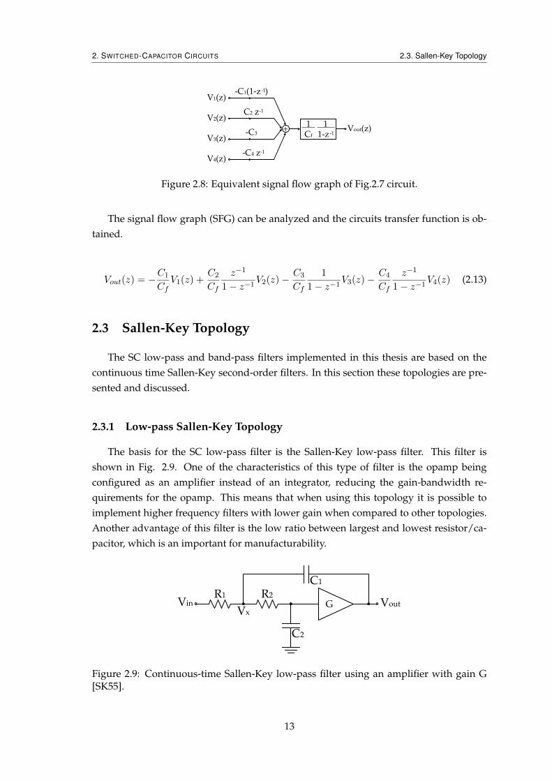
2.8 Equivalent signal flow graph of Fig.2.7 circuit. . . . . . . . . . . . . . . . . 13
2.9 Continuous-time Sallen-Key low-pass filter using an amplifier with gain G[SK55]. . . . . . . . . . . . . . . . . . . . . . . . . . . . . . . . . . . . . . . . 13
2.10 Continuous-time Sallen-Key band-pass filter. . . . . . . . . . . . . . . . . . 14
3.1 Continuous-time Sallen-Key low-pass filter. . . . . . . . . . . . . . . . . . . 17
3.2 Single-ended low-pass SC filter. . . . . . . . . . . . . . . . . . . . . . . . . . 18
3.3 Low-pass SC filter during: (a) Clock phase 1 (b) Clock phase 2 . . . . . . . 18
3.4 Discrete-time frequency responses. . . . . . . . . . . . . . . . . . . . . . . . 20
3.5 Capacitor in single-ended (a) and differential configuration (b) . . . . . . . 20
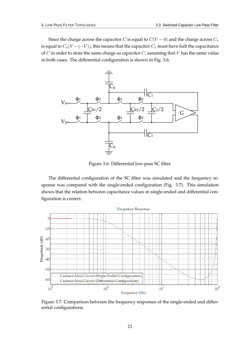
3.6 Differential low-pass SC filter. . . . . . . . . . . . . . . . . . . . . . . . . . . 21
3.7 Comparison between the frequency responses of the single-ended and dif-ferential configurations. . . . . . . . . . . . . . . . . . . . . . . . . . . . . . 21
3.8 Frequency response of each second-order section . . . . . . . . . . . . . . . 23
3.9 Frequency Response of the sixth-order filter . . . . . . . . . . . . . . . . . . 23
4.1 Continuous-time Sallen-Key band-pass filter. . . . . . . . . . . . . . . . . . 25
4.2 Single-ended band-pass SC filter. . . . . . . . . . . . . . . . . . . . . . . . . 26
4.3 Band-pass SC filter during: (a) Clock phase 1 (b) Clock phase 2 . . . . . . . 26
4.4 Discrete-time frequency responses. . . . . . . . . . . . . . . . . . . . . . . . 28
4.5 Differential band-pass SC filter. . . . . . . . . . . . . . . . . . . . . . . . . . 28
xv
xvi LIST OF FIGURES
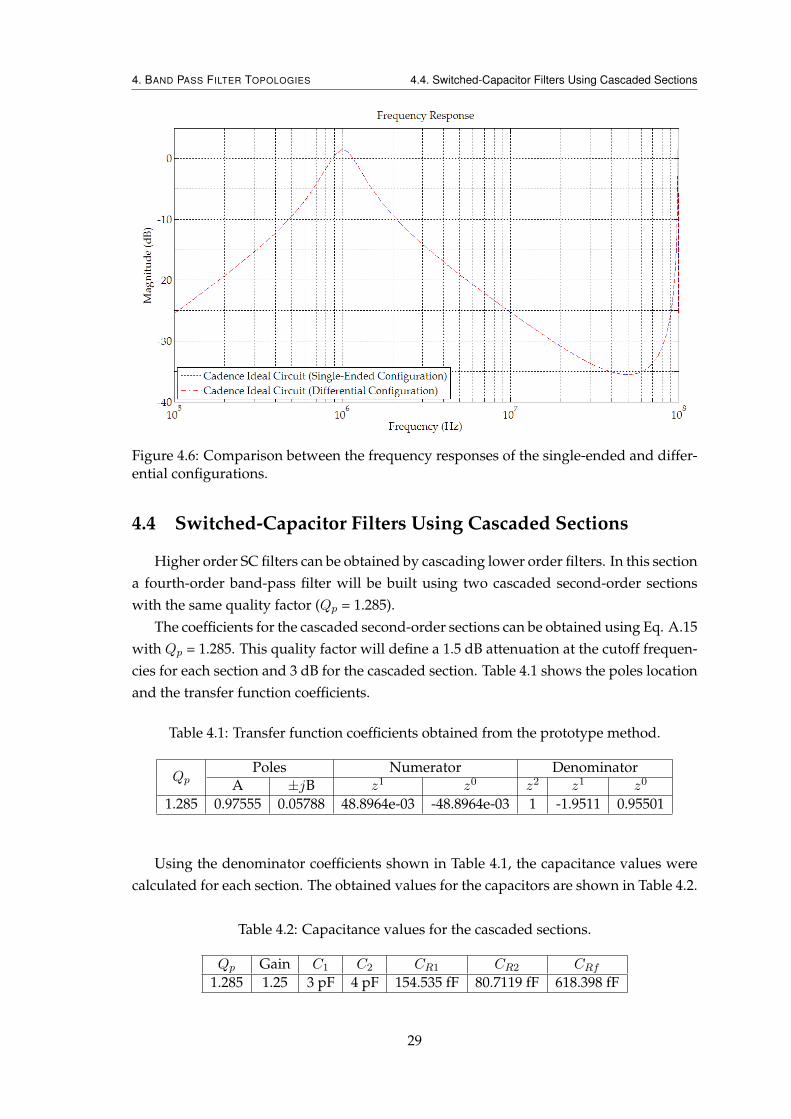
4.6 Comparison between the frequency responses of the single-ended and dif-ferential configurations. . . . . . . . . . . . . . . . . . . . . . . . . . . . . . 29
4.7 Frequency response of the second-order section . . . . . . . . . . . . . . . 30
4.8 Frequency response of the fourth-order filter . . . . . . . . . . . . . . . . . 30
5.1 Passive first-order low-pass filter. . . . . . . . . . . . . . . . . . . . . . . . . 32
5.2 First-order low-pass SC filter. . . . . . . . . . . . . . . . . . . . . . . . . . . 32
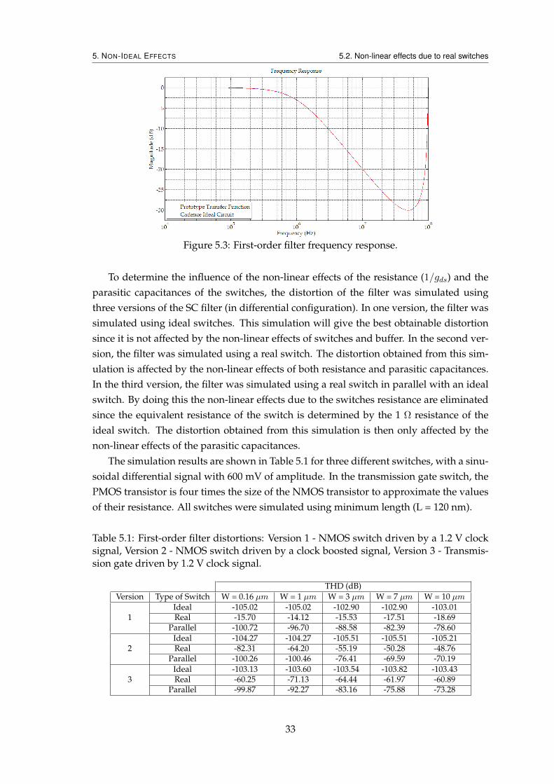
5.3 First-order filter frequency response. . . . . . . . . . . . . . . . . . . . . . . 33
5.4 Ideal charge pump representation. . . . . . . . . . . . . . . . . . . . . . . . 35
5.5 Clock boost circuit [DK99]. . . . . . . . . . . . . . . . . . . . . . . . . . . . . 36
5.6 Clock boost circuit considering parasitic capacitances. . . . . . . . . . . . . 36
5.7 Simplified clock boost circuit considering parasitic capacitances. . . . . . . 37
5.8 Simplified clock boost circuit during: (a) Clock phase 1 (b) Clock phase 2 . 37
5.9 Clock boosted phase 1. . . . . . . . . . . . . . . . . . . . . . . . . . . . . . . 38
5.10 Effect of clock boosting on the switches conductance . . . . . . . . . . . . . 39
5.11 Clock boost circuit [MS12]. . . . . . . . . . . . . . . . . . . . . . . . . . . . . 39
5.12 Phase overlap due to clock speed increase beyond the circuit bandwidth. . 40
5.13 Voltage boosting at 10 MHz. . . . . . . . . . . . . . . . . . . . . . . . . . . . 41
5.14 Clock boosted phase 1 for three different supply voltages. . . . . . . . . . . 41
5.15 Effect of clock boosting on the switches conductance for three differentsupply voltages. . . . . . . . . . . . . . . . . . . . . . . . . . . . . . . . . . . 42
5.16 Distortion with and without clock boosting in function of the switches width. 42
5.17 Basic buffer topology. . . . . . . . . . . . . . . . . . . . . . . . . . . . . . . . 43
5.18 Source follower with gds compensation. . . . . . . . . . . . . . . . . . . . . 44
5.19 Source follower with gds compensation low frequency small signal model. 44
5.20 Source follower with gds compensation low frequency small signal modelconsidering thermal noise. . . . . . . . . . . . . . . . . . . . . . . . . . . . . 45
5.21 Source follower with gds compensation medium frequency small signalmodel. . . . . . . . . . . . . . . . . . . . . . . . . . . . . . . . . . . . . . . . 46
5.22 Complementary source follower with gds compensation. . . . . . . . . . . 46
5.23 Complementary source follower with gds compensation low frequency smallsignal model. . . . . . . . . . . . . . . . . . . . . . . . . . . . . . . . . . . . 47
5.24 Complementary source follower with gds compensation low frequency smallsignal model considering thermal noise. . . . . . . . . . . . . . . . . . . . . 47
5.25 Complementary source follower with gds compensation medium frequencysmall signal model. . . . . . . . . . . . . . . . . . . . . . . . . . . . . . . . . 48
5.26 Source follower with gds and body effect compensation: (a) Normal ver-sion (b) Complementary version . . . . . . . . . . . . . . . . . . . . . . . . 49
5.27 Source follower with gds and body effect compensation low frequency smallsignal model. . . . . . . . . . . . . . . . . . . . . . . . . . . . . . . . . . . . 49
LIST OF FIGURES xvii
5.28 Source follower with gds and body effect compensation low frequency smallsignal model considering thermal noise. . . . . . . . . . . . . . . . . . . . . 50
5.29 Source follower with gds and body effect compensation medium frequencysmall signal model. . . . . . . . . . . . . . . . . . . . . . . . . . . . . . . . . 50
5.30 Relationship between the gain of the circuits and the DC voltage. . . . . . 51
5.31 Basic single-ended topology. . . . . . . . . . . . . . . . . . . . . . . . . . . . 55
5.32 Single-ended configuration of the voltage-combiner amplifier. . . . . . . . 55
5.33 Voltage-combiner amplifier low frequency small signal model. . . . . . . . 55
5.34 Voltage-combiner amplifier low frequency small signal model consideringthermal noise. . . . . . . . . . . . . . . . . . . . . . . . . . . . . . . . . . . . 56
5.35 Voltage-combiner amplifier medium frequency small signal model. . . . . 57
5.36 Single-ended configuration of the complementary voltage-combiner am-plifier. . . . . . . . . . . . . . . . . . . . . . . . . . . . . . . . . . . . . . . . . 57
5.37 Complementary voltage-combiner amplifier low frequency small signalmodel. . . . . . . . . . . . . . . . . . . . . . . . . . . . . . . . . . . . . . . . 58
5.38 Complementary voltage-combiner amplifier low frequency small signalmodel considering thermal noise. . . . . . . . . . . . . . . . . . . . . . . . . 58
5.39 Complementary voltage-combiner amplifier medium frequency small sig-nal model. . . . . . . . . . . . . . . . . . . . . . . . . . . . . . . . . . . . . . 59
5.40 Relation between the gain of the circuits and the DC voltage. . . . . . . . . 60
5.41 Complementary differential folded amplifier with source degeneration us-ing MOS transistors. . . . . . . . . . . . . . . . . . . . . . . . . . . . . . . . 61
6.1 Low-pass SC filter considering parasitic capacitances. . . . . . . . . . . . . 64
6.2 Clock boost (a) and buffer (b) used in this section . . . . . . . . . . . . . . . 64
6.3 Frequency responses of the second-order filter. . . . . . . . . . . . . . . . . 65
6.4 Clock boost (a) and amplifier (b) used in this section . . . . . . . . . . . . . 66
6.5 Frequency responses of the second-order filter at 1.2 V. . . . . . . . . . . . 67
6.6 Frequency responses of the second-order filter at 0.9 V. . . . . . . . . . . . 68
6.7 Clock boost (a) and buffer (b) used in this section . . . . . . . . . . . . . . . 69
6.8 Frequency responses of the low quality factor filter. . . . . . . . . . . . . . 69
6.9 Clock boost (a) and buffer (b) used in this section . . . . . . . . . . . . . . . 70
6.10 Frequency responses of the medium quality factor filter. . . . . . . . . . . . 70
6.11 Clock boost (a) and buffer (b) used in this section . . . . . . . . . . . . . . . 71
6.12 Frequency responses of the high quality factor filter. . . . . . . . . . . . . . 72
6.13 Frequency responses of the sixth-order filter. . . . . . . . . . . . . . . . . . 72
6.14 Band-pass SC filter considering parasitic capacitances. . . . . . . . . . . . . 73
6.15 Clock boost (a) and amplifier (b) used in this section . . . . . . . . . . . . . 74
6.16 Frequency responses of the filter. . . . . . . . . . . . . . . . . . . . . . . . . 75
6.17 Clock boost (a) and amplifier (b) used in this section . . . . . . . . . . . . . 76
6.18 Frequency responses of the first section of the filter. . . . . . . . . . . . . . 76
xviii LIST OF FIGURES
6.19 Clock boost (a) and amplifier (b) used in this section . . . . . . . . . . . . . 776.20 Frequency responses of the second section of the filter. . . . . . . . . . . . 776.21 Frequency responses of the fourth-order filter. . . . . . . . . . . . . . . . . 78
B.1 Procedure to obtain transfer function from a SC filter. . . . . . . . . . . . . 89
List of Tables
2.1 SC resistor emulation circuits [AH02]. . . . . . . . . . . . . . . . . . . . . . 9
2.2 Charge in the capacitors in each phase. . . . . . . . . . . . . . . . . . . . . . 10
2.3 Charge in the capacitors in each phase. . . . . . . . . . . . . . . . . . . . . . 11
2.4 Charge in the capacitors in each phase. . . . . . . . . . . . . . . . . . . . . . 12
3.1 Transfer function coefficients obtained from Matlab. . . . . . . . . . . . . . 22
3.2 Capacitance values for each section. . . . . . . . . . . . . . . . . . . . . . . 22
4.1 Transfer function coefficients obtained from the prototype method. . . . . 29
4.2 Capacitance values for the cascaded sections. . . . . . . . . . . . . . . . . . 29
5.1 First-order filter distortions: Version 1 - NMOS switch driven by a 1.2 Vclock signal, Version 2 - NMOS switch driven by a clock boosted signal,Version 3 - Transmission gate driven by 1.2 V clock signal. . . . . . . . . . 33
5.2 Influence of the resistance and parasitic capacitances in the overall distor-tion: Version 1 - NMOS switch driven by a 1.2 V clock signal, Version 2 -NMOS switch driven by a clock boosted signal, Version 3 - Transmissiongate driven by 1.2 V clock signal. . . . . . . . . . . . . . . . . . . . . . . . . 34
5.3 Simulated clock boost circuit parasitic capacitance values. . . . . . . . . . 38
5.4 HSL130E transistor parameters: (a) Source follower (SF) with gds compen-sation with DC @ 0.6 V (b) Complementary source follower (CSF) with gdscompensation with DC @ 0.6 V (c) SF with gds compensation with DC @0.45 V (d) CSF with gds compensation with DC @ 0.75 V. . . . . . . . . . . . 52
5.5 RF_12 transistor parameters: (a) Source follower with gds compensationwith DC @ 0.6 V (b) Complementary source follower with gds compensa-tion with DC @ 0.6 V (c) Source follower with gds compensation with DC@ 0.45 V (d) Complementary source follower with gds compensation withDC @ 0.75 V. . . . . . . . . . . . . . . . . . . . . . . . . . . . . . . . . . . . . 53
xix
xx LIST OF TABLES
5.6 Simulation results for the buffers with a common mode voltage of 0.6 V:(a) Source follower (SF) with gds compensation (b) Complementary sourcefollower (CSF) with gds compensation (c) SF with gds and body effect com-pensation (d) CSF with gds and body effect compensation. . . . . . . . . . 53
5.7 Simulated results for the buffers with a common mode voltage of 0.45/0.75V: (a) Source follower (SF) with gds compensation (b) Complementary sourcefollower (CSF) with gds compensation (c) SF with gds and body effect com-pensation (d) CSF with gds and body effect compensation. . . . . . . . . . 54
5.8 Simulated results for the amplifiers with a common mode voltage of 0.6V: (a) Differential folded amplifier (b) Complementary differential foldedamplifier. . . . . . . . . . . . . . . . . . . . . . . . . . . . . . . . . . . . . . . 61
5.9 Simulated results for the complementary differential folded amplifier withsource degeneration. . . . . . . . . . . . . . . . . . . . . . . . . . . . . . . . 62
5.10 Transistor parameters: (a) Differential folded amplifier (DFA) with supply@ 1.2 V (b) DFA with supply @ 0.9 V (c) Complementary differential foldedamplifier (CDFA) with supply @ 1.2 V (d) CDFA with supply @ 0.9 V. . . . 62
6.1 Filter capacitances and distortion results: (a) Using ideal components (b)Using real buffers (c) Using real switches (d) Using real components. (?single-ended capacitor) . . . . . . . . . . . . . . . . . . . . . . . . . . . . . . 65
6.2 Filter capacitances and distortion results: (a) Using ideal components (b)Using real amplifiers (c) Using real switches (d) Using real components. (?single-ended capacitor) . . . . . . . . . . . . . . . . . . . . . . . . . . . . . . 66
6.3 Filter capacitances and distortion results: (a) Using ideal components (b)Using real amplifiers (c) Using real switches (d) Using real components. (?single-ended capacitor) . . . . . . . . . . . . . . . . . . . . . . . . . . . . . . 67
6.4 Filter capacitances and distortion results: (a) Using ideal components (b)Using real buffers (c) Using real switches (d) Using real components. (?single-ended capacitor) . . . . . . . . . . . . . . . . . . . . . . . . . . . . . . 69
6.5 Filter capacitances and distortion results: (a) Using ideal components (b)Using real buffers (c) Using real switches (d) Using real components. (?single-ended capacitor) . . . . . . . . . . . . . . . . . . . . . . . . . . . . . . 70
6.6 Filter capacitances and distortion results: (a) Using ideal components (b)Using real buffers (c) Using real switches (d) Using real components. (?single-ended capacitor) . . . . . . . . . . . . . . . . . . . . . . . . . . . . . . 71
6.7 Filter capacitances: (a) Using ideal components (b) Using real switches (c)Using real components. (? single-ended capacitor) . . . . . . . . . . . . . . 74
6.8 Filter capacitances: (a) Using ideal components (b) Using real switches (c)Using real components. (? single-ended capacitor) . . . . . . . . . . . . . . 75
6.9 Filter capacitances: (a) Using ideal components (b) Using real switches (c)Using real components. (? single-ended capacitor) . . . . . . . . . . . . . . 77
LIST OF TABLES xxi
A.1 Obtaining the Butterworth transfer function coefficients using Matlab fora continuous-time low-pass filter. . . . . . . . . . . . . . . . . . . . . . . . . 83
A.2 Obtaining the Butterworth transfer function coefficients using Matlab fora discrete-time low-pass filter. . . . . . . . . . . . . . . . . . . . . . . . . . . 85
A.3 Obtaining the Butterworth transfer function poles using Matlab for a discrete-time low-pass filter. . . . . . . . . . . . . . . . . . . . . . . . . . . . . . . . . 85
A.4 Obtaining the Butterworth transfer function coefficients using Matlab fora continuous band-pass filter. . . . . . . . . . . . . . . . . . . . . . . . . . . 86
A.5 Obtaining the Butterworth transfer function coefficients using Matlab fora discrete band-pass filter. . . . . . . . . . . . . . . . . . . . . . . . . . . . . 87
B.1 Example of how to plot the Bode Diagram. . . . . . . . . . . . . . . . . . . 90

xxii LIST OF TABLES
Abbreviations
A/D Analog/Digital
CDFA Complementary Differential Folded Amplifier
CMOS Complementary Metal-Oxide-Semiconductor
CSF Complementary Source Follower
D/A Digital/Analog
DFA Differential Folded Amplifier
FOM Figure Of Merit
IC Integrated Circuit
KCL Kirchhoff’s Current Law
KVL Kirchhoff’s Voltage Law
MOSFET Metal-Oxide-Semiconductor Field-Effect Transistor
OpAmp Operational Amplifier
SC Switched-Capacitor
SF Source Follower
SFG Signal Flow Graph
VCVS Voltage Controlled Voltage Source
xxiii

xxiv
1Introduction
1.1 Background and Motivation
Interest in switched-capacitor networks started in the late 70s due to the possibilityof implementing analog filters using monolithic integrated circuit (IC) technology andbecause it is possible to obtain a good accuracy in the ratio between two capacitor values.Since typically high value resistors are needed in the implementation of analog filters,they can be generated using small on-chip capacitors, which makes it an attractive optionfor monolithic fabrication, since it occupies a small substrate area.
SC circuits operate as discrete-time circuits without the use of converters (A/D orD/A). When used as filters, these circuits have an accurate frequency response, goodlinearity, and good dynamic range. The accuracy of these circuits comes from the timeconstants being determined by capacitor ratios, which in real applications can have anaccuracy of nearly 0.1% while in integrated RC circuits the time constant error can rangefrom 20% to 50%. Another advantage is the incorporation of a certain degree of frequencytuning by varying the clock frequency [CJM12].
Although there are several advantages in using this type of technology, there are alsoseveral non-ideal properties that need to be considered, like clock feedthrough, offseterror, noise, and parasitic capacitances [CRCR77]. Usually SC filters need an antialiasingfilter at the input and a smoothing filter at the output [GT86].
The scaling-down of transistors in advanced deep-submicron CMOS technologiesresults in the reduction of the intrinsic gain (gm/gds), making the design of high gainopamps increasingly difficult. This limitation has large impact on the performance offilter circuits.
The objective of this thesis is to study the low-pass and band-pass Sallen-Key topolo-gies since they do not require high gain amplifiers. The strategy used is to replace theopamp with a voltage buffer. Doing this simplifies the design of the amplifier although
1
1. INTRODUCTION 1.2. Thesis Organization
it also eliminates the virtual ground node from the circuit. Without this node, parasiticinsensitive SC networks cannot be used. Due to modern parasitic extraction softwarethat can reliably predict the values of parasitic capacitances, the historical disadvantageof parasitic sensitive SC networks (parallel SC) is no longer critical, allowing its influenceto be compensated during the design process.
Since the first SC circuits used parallel SC networks, the filter topologies studied inthis thesis will be converted to SC circuits using this type of network, and the topologiesadapted, if need be, to work in modern nm CMOS technologies.
1.2 Thesis Organization
Besides this introductory chapter, this thesis is organized in six more chapters.In Chapter 2, an overview of SC filters and their main building blocks is presented,
including advantages and non-ideal properties that need to be considered in this type ofcircuits. SC resistor emulation networks are also presented and an integrator is describedusing two different networks in order to show the advantage of using certain SC net-works to neglect non-ideal properties when an amplifier is used. The transfer functionsof the low-pass and band-pass Sallen-Key topologies are also presented in this chapter.
In Chapter 3, the low-pass near-unity gain Sallen-Key topology is presented alongwith the design equations and transfer function. Using this topology and adapting it,a SC single-ended version is obtained. The design equations and transfer function arealso presented, and the topology is simulated using ideal components. The differentialconfiguration of the low-pass SC filter is presented. A sixth-order filter is also obtainedby cascading biquadratic sections and simulated using ideal components.
Chapter 4 has the same structure as the previous chapter, but a band-pass filter is con-sidered and a fourth-order filter is obtained from cascading biquadratic sections (insteadof a sixth-order filter).
In Chapter 5, the non-ideal effects that result from using real components are de-scribed. The non-linear effects due to real switches is studied using different types ofswitches in a first-order SC filter and varying the switches size. Two clock boost cir-cuits that can be used to reduce the non-linear effects of switches are presented, and theswitches conductance with and without the use of these circuits is compared. One ofthese circuits is capable of operating at lower voltages. Two different buffers are also pre-sented, in normal and in complementary configurations, along with low frequency gain,high frequency gain and noise equations.
In Chapter 6, the filter circuits are simulated using real components. The results ofthe simulations are presented when all components are ideal, when the switches are realand the remaining components ideal, when the buffers/amplifiers are real and the re-maining components ideal, and when all components are real in order to determine theinfluence of each real component in the overall performance of the filter. The circuitsinclude second-order low-pass filters, two operating at 1.2 V using the buffers presented
2
1. INTRODUCTION 1.3. Contributions
in the previous chapter, one operating at 0.9 V, and a sixth-order filter obtained from cas-cading three biquadratic sections operating at 1.2 V. The band-pass filter circuit was alsosimulated for a second-order filter, and a fourth-order filter obtained from cascading twobiquadratic sections, all operating at 1.2 V.
In the seventh and last chapter, the results obtained are discussed and the conclusionsof these work are presented. Using these conclusions further possible research sugges-tions are advised.
1.3 Contributions
The main contribution of this thesis is the implementation of SC filters based on theSallen-Key topology (low-pass and band-pass) using near-unity gain amplifiers. This re-quired the compensation of parasitic capacitances due to the filters sensitivity to thesenon-linear effects when the virtual ground of an amplifier is not present. To minimizethese non-linear effects, different switch configurations (NMOS switch, clock boostedNMOS switch, and transmission gate switch) were studied to determine the switch withbest performance, and in which conditions (switches width) in order to facilitate the com-pensation of these effects. To reduce the filters harmonic distortion, different techniques(common mode voltage adjustment and source degeneration) were successfully used. Alow voltage version of a low-pass filter was also implemented.
Different parts of the work developed in this thesis are being used to submit papers tothe IEEE International Symposium on Circuits and Systems (ISCAS) and Doctoral Con-ference on Computing, Electrical and Industrial Systems (DoCEIS).
3
1. INTRODUCTION 1.3. Contributions
4
2Switched-Capacitor Circuits
2.1 Switched-Capacitor Filters Building Blocks
SC filters can be implemented using switches, capacitors, opamps, and non-overlappingclock generators.
2.1.1 Operational Amplifiers
Opamps in SC circuits provide a virtual ground node. Parasitic capacitances con-nected to this node do not influence the performance of the circuit, since they will beconnected to ground during one clock phase and to the virtual ground during the other.Opamps also have non-ideal effects that affect the performance of SC circuits like DCgain, unity gain frequency and phase margin, slew-rate, and common mode voltage.
2.1.2 Switches
SC circuits require switches with high off resistance in order to minimize the chargeleakage when the switches are open, and low on resistance so that the circuit can settlein less than half a clock period. MOSFET transistors satisfy both these requirements,since they have very high off resistance and low on resistance (GΩ and kΩ, respectively),depending on the transistors size. Increasing the width of the transistor will decrease thevalue of both of these resistances.
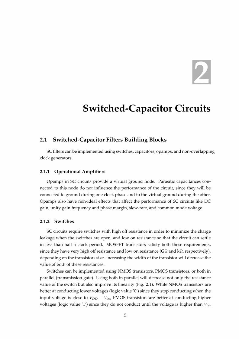
Switches can be implemented using NMOS transistors, PMOS transistors, or both inparallel (transmission gate). Using both in parallel will decrease not only the resistancevalue of the switch but also improve its linearity (Fig. 2.1). While NMOS transistors arebetter at conducting lower voltages (logic value ’0’) since they stop conducting when theinput voltage is close to VDD − Vtn, PMOS transistors are better at conducting highervoltages (logic value ’1’) since they do not conduct until the voltage is higher than Vtp.
5
2. SWITCHED-CAPACITOR CIRCUITS 2.1. Switched-Capacitor Filters Building Blocks
Transmission gates are good at transmitting ’0’s and ’1’s since lower voltages will travelvia the NMOS transistor and higher voltages will travel via the PMOS transistor.
RdsPMOS RdsNMOS
Transmission Gate (Parallel)
Figure 2.1: Example of the rds resistance of MOS transistors as function of the Vin(Vs)voltage.
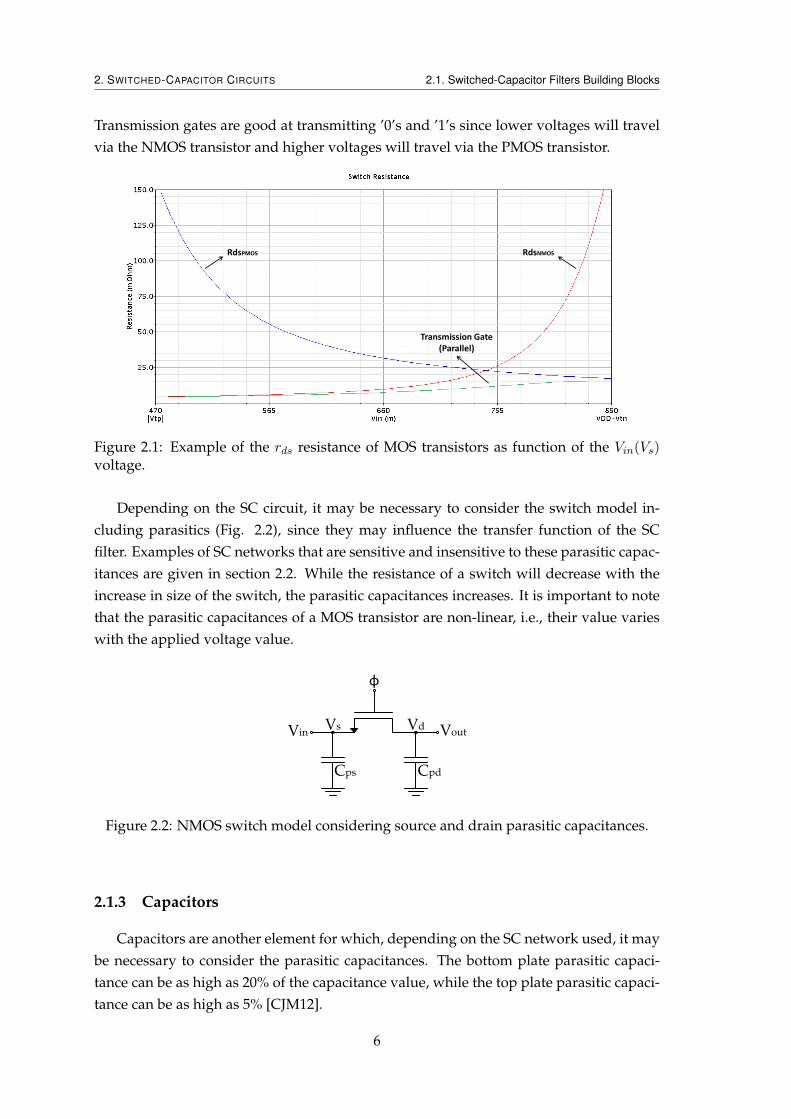
Depending on the SC circuit, it may be necessary to consider the switch model in-cluding parasitics (Fig. 2.2), since they may influence the transfer function of the SCfilter. Examples of SC networks that are sensitive and insensitive to these parasitic capac-itances are given in section 2.2. While the resistance of a switch will decrease with theincrease in size of the switch, the parasitic capacitances increases. It is important to notethat the parasitic capacitances of a MOS transistor are non-linear, i.e., their value varieswith the applied voltage value.
φ
CpdCps
VoutVinVs Vd
Figure 2.2: NMOS switch model considering source and drain parasitic capacitances.
2.1.3 Capacitors
Capacitors are another element for which, depending on the SC network used, it maybe necessary to consider the parasitic capacitances. The bottom plate parasitic capaci-tance can be as high as 20% of the capacitance value, while the top plate parasitic capaci-tance can be as high as 5% [CJM12].
6
2. SWITCHED-CAPACITOR CIRCUITS 2.2. Switched-Capacitor Resistor Emulation Networks
2.1.4 Non-Overlapping Clock Phases
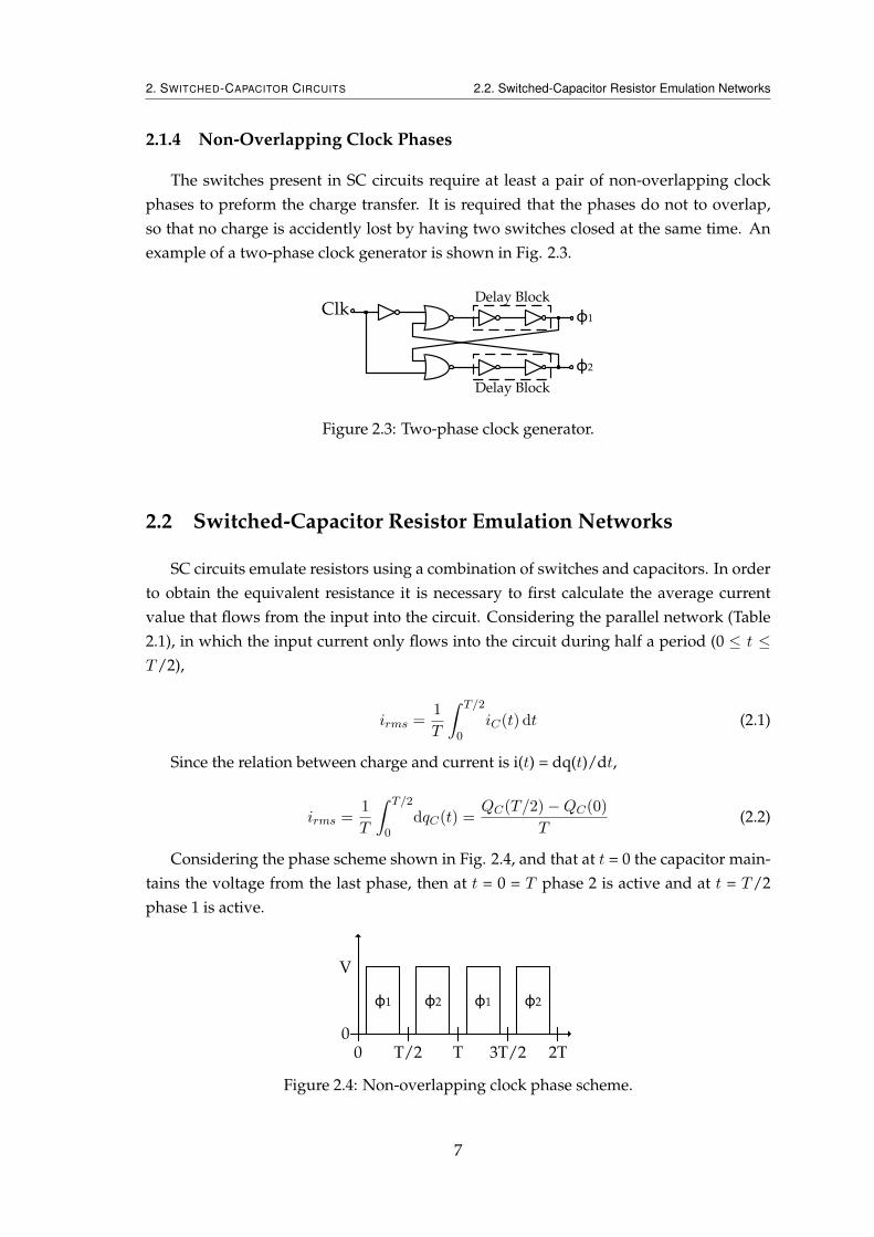
The switches present in SC circuits require at least a pair of non-overlapping clockphases to preform the charge transfer. It is required that the phases do not to overlap,so that no charge is accidently lost by having two switches closed at the same time. Anexample of a two-phase clock generator is shown in Fig. 2.3.
Clk φ1
φ2
Delay Block
Delay Block
Figure 2.3: Two-phase clock generator.
2.2 Switched-Capacitor Resistor Emulation Networks
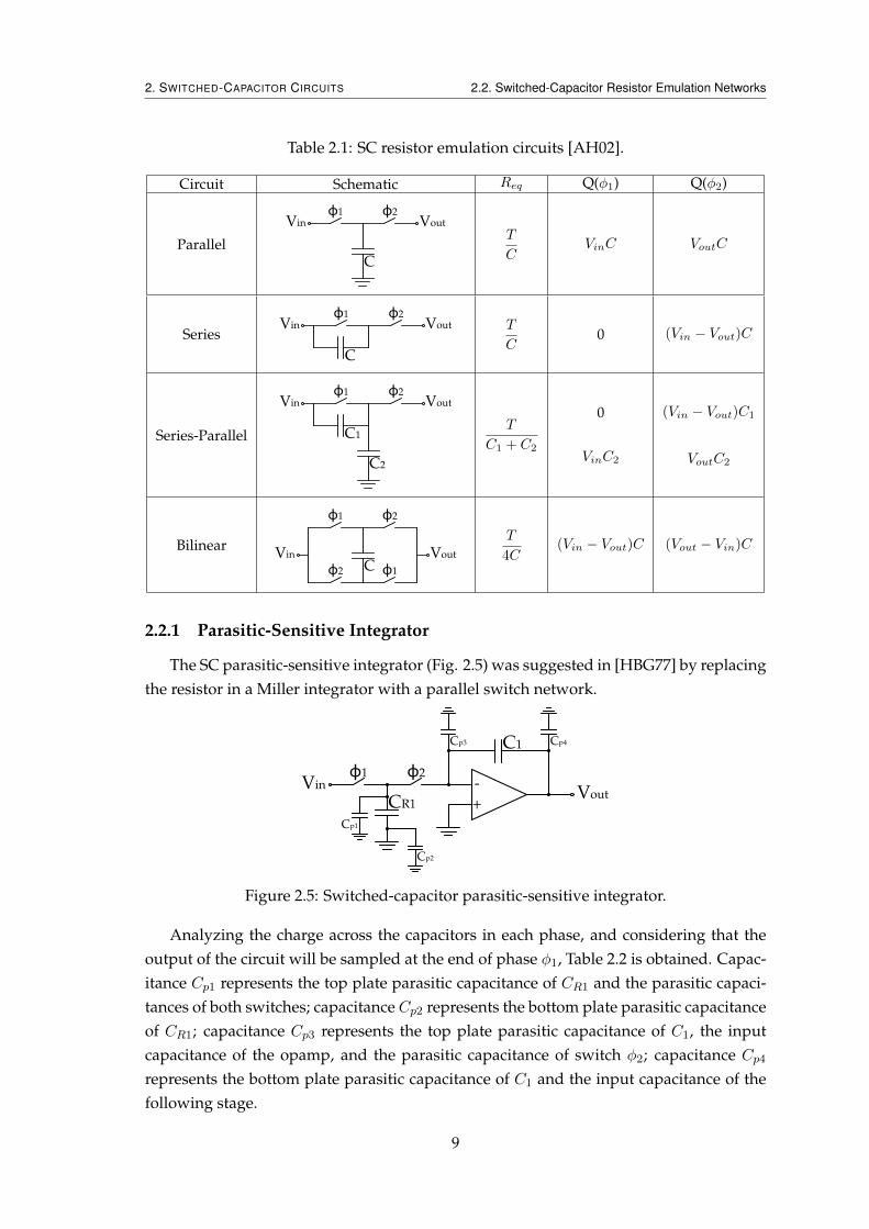
SC circuits emulate resistors using a combination of switches and capacitors. In orderto obtain the equivalent resistance it is necessary to first calculate the average currentvalue that flows from the input into the circuit. Considering the parallel network (Table2.1), in which the input current only flows into the circuit during half a period (0 ≤ t ≤T/2),
irms =1
T
∫ T/2
0iC(t) dt (2.1)
Since the relation between charge and current is i(t) = dq(t)/dt,
irms =1
T
∫ T/2
0dqC(t) =
QC(T/2)−QC(0)
T(2.2)
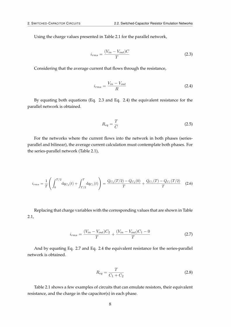
Considering the phase scheme shown in Fig. 2.4, and that at t = 0 the capacitor main-tains the voltage from the last phase, then at t = 0 = T phase 2 is active and at t = T/2phase 1 is active.
φ1
V
0
φ1φ2 φ2
T/2 T 3T/2 2T0
Figure 2.4: Non-overlapping clock phase scheme.
7
2. SWITCHED-CAPACITOR CIRCUITS 2.2. Switched-Capacitor Resistor Emulation Networks
Using the charge values presented in Table 2.1 for the parallel network,
irms =(Vin − Vout)C
T(2.3)
Considering that the average current that flows through the resistance,
irms =Vin − Vout
R(2.4)
By equating both equations (Eq. 2.3 and Eq. 2.4) the equivalent resistance for theparallel network is obtained.
Req =T
C(2.5)
For the networks where the current flows into the network in both phases (series-parallel and bilinear), the average current calculation must contemplate both phases. Forthe series-parallel network (Table 2.1),
irms =1
T
(∫ T/2
0
dqC2(t) +
∫ T
T/2
dqC1(t)
)=QC2
(T/2)−QC2(0)
T+QC1
(T )−QC1(T/2)
T(2.6)
Replacing that charge variables with the corresponding values that are shown in Table2.1,
irms =(Vin − Vout)C2
T+
(Vin − Vout)C1 − 0
T(2.7)
And by equating Eq. 2.7 and Eq. 2.4 the equivalent resistance for the series-parallelnetwork is obtained.
Req =T
C1 + C2(2.8)
Table 2.1 shows a few examples of circuits that can emulate resistors, their equivalentresistance, and the charge in the capacitor(s) in each phase.
8
2. SWITCHED-CAPACITOR CIRCUITS 2.2. Switched-Capacitor Resistor Emulation Networks
Table 2.1: SC resistor emulation circuits [AH02].
Circuit Schematic Req Q(φ1) Q(φ2)
Parallel
Vinφ1 φ2
C
Vout
T
CVinC VoutC
Seriesφ1
C
Voutφ2
Vin T
C0 (Vin − Vout)C
Series-Parallel
φ1
C1
Voutφ2
C2
Vin
T
C1 + C2
0
VinC2
(Vin − Vout)C1
VoutC2
BilinearVin
φ1 φ2
CVout
φ2 φ1
T
4C(Vin − Vout)C (Vout − Vin)C
2.2.1 Parasitic-Sensitive Integrator
The SC parasitic-sensitive integrator (Fig. 2.5) was suggested in [HBG77] by replacingthe resistor in a Miller integrator with a parallel switch network.
Vout-
+
Vin
CR1
φ1 φ2
C1
Cp1
Cp2
Cp3 Cp4
Figure 2.5: Switched-capacitor parasitic-sensitive integrator.
Analyzing the charge across the capacitors in each phase, and considering that theoutput of the circuit will be sampled at the end of phase φ1, Table 2.2 is obtained. Capac-itance Cp1 represents the top plate parasitic capacitance of CR1 and the parasitic capaci-tances of both switches; capacitance Cp2 represents the bottom plate parasitic capacitanceof CR1; capacitance Cp3 represents the top plate parasitic capacitance of C1, the inputcapacitance of the opamp, and the parasitic capacitance of switch φ2; capacitance Cp4
represents the bottom plate parasitic capacitance of C1 and the input capacitance of thefollowing stage.
9
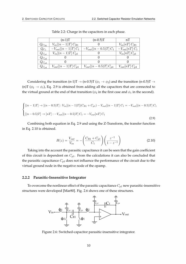
2. SWITCHED-CAPACITOR CIRCUITS 2.2. Switched-Capacitor Resistor Emulation Networks
Table 2.2: Charge in the capacitors in each phase.
(n-1)T (n-0.5)T nTQCR1
Vin[(n− 1)T ] CR1 0 Vin[nT ] CR1
QC1 −Vout[(n− 1)T ] C1 −Vout[(n− 0.5)T ] C1 −Vout[nT ] C1
QCp1 Vin[(n− 1)T ] Cp1 0 Vin[nT ] Cp1
QCp2 0 0 0QCp3 0 0 0QCp4 Vout[(n− 1)T ] Cp4 Vout[(n− 0.5)T ] Cp4 Vout[nT ] Cp4
Considering the transition (n-1)T→ (n-0.5)T (φ1 → φ2) and the transition (n-0.5)T→(n)T (φ2 → φ1), Eq. 2.9 is obtained from adding all the capacitors that are connected tothe virtual ground at the end of that transition (φ2 in the first case and φ1 in the second).
[(n− 1)T ]→ [(n− 0.5)T ] : Vin[(n− 1)T ](CR1 + Cp1)− Vout[(n− 1)T ] C1 = −Vout[(n− 0.5)T ] C1
[(n− 0.5)T ]→ [nT ] : −Vout[(n− 0.5)T ] C1 = −Vout[nT ] C1
(2.9)
Combining both equation in Eq. 2.9 and using the Z-Transform, the transfer functionin Eq. 2.10 is obtained.
H(z) =VoutVin
= −
(CR1 + Cp1
C1
)(z−1
1− z−1
)(2.10)
Taking into the account the parasitic capacitance it can be seen that the gain coefficientof this circuit is dependent on Cp1. From the calculations it can also be concluded thatthe parasitic capacitance Cp3 does not influence the performance of the circuit due to thevirtual ground node in the negative node of the opamp.
2.2.2 Parasitic-Insensitive Integrator
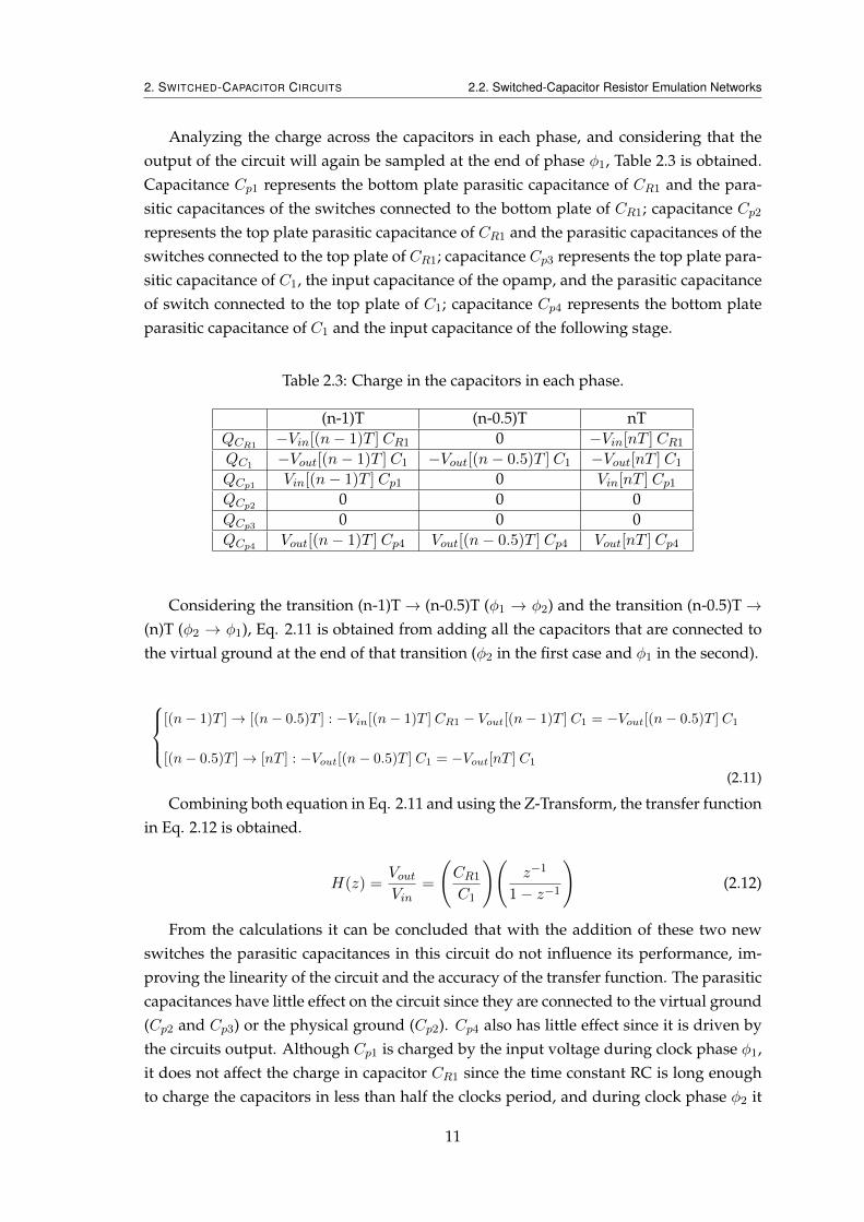
To overcome the nonlinear effect of the parasitic capacitanceCp1 new parasitic-insensitivestructures were developed [Mar80]. Fig. 2.6 shows one of these structures.
Vout-
+
Vin
CR1
φ1 φ2
C1
Cp2
Cp3 Cp4
φ2
Cp1
φ1
Figure 2.6: Switched-capacitor parasitic-insensitive integrator.
10
2. SWITCHED-CAPACITOR CIRCUITS 2.2. Switched-Capacitor Resistor Emulation Networks
Analyzing the charge across the capacitors in each phase, and considering that theoutput of the circuit will again be sampled at the end of phase φ1, Table 2.3 is obtained.Capacitance Cp1 represents the bottom plate parasitic capacitance of CR1 and the para-sitic capacitances of the switches connected to the bottom plate of CR1; capacitance Cp2
represents the top plate parasitic capacitance of CR1 and the parasitic capacitances of theswitches connected to the top plate of CR1; capacitance Cp3 represents the top plate para-sitic capacitance of C1, the input capacitance of the opamp, and the parasitic capacitanceof switch connected to the top plate of C1; capacitance Cp4 represents the bottom plateparasitic capacitance of C1 and the input capacitance of the following stage.
Table 2.3: Charge in the capacitors in each phase.
(n-1)T (n-0.5)T nTQCR1
−Vin[(n− 1)T ] CR1 0 −Vin[nT ] CR1
QC1 −Vout[(n− 1)T ] C1 −Vout[(n− 0.5)T ] C1 −Vout[nT ] C1
QCp1 Vin[(n− 1)T ] Cp1 0 Vin[nT ] Cp1
QCp2 0 0 0QCp3 0 0 0QCp4 Vout[(n− 1)T ] Cp4 Vout[(n− 0.5)T ] Cp4 Vout[nT ] Cp4
Considering the transition (n-1)T→ (n-0.5)T (φ1 → φ2) and the transition (n-0.5)T→(n)T (φ2 → φ1), Eq. 2.11 is obtained from adding all the capacitors that are connected tothe virtual ground at the end of that transition (φ2 in the first case and φ1 in the second).
[(n− 1)T ]→ [(n− 0.5)T ] : −Vin[(n− 1)T ] CR1 − Vout[(n− 1)T ] C1 = −Vout[(n− 0.5)T ] C1
[(n− 0.5)T ]→ [nT ] : −Vout[(n− 0.5)T ] C1 = −Vout[nT ] C1
(2.11)
Combining both equation in Eq. 2.11 and using the Z-Transform, the transfer functionin Eq. 2.12 is obtained.
H(z) =VoutVin
=
(CR1
C1
)(z−1
1− z−1
)(2.12)
From the calculations it can be concluded that with the addition of these two newswitches the parasitic capacitances in this circuit do not influence its performance, im-proving the linearity of the circuit and the accuracy of the transfer function. The parasiticcapacitances have little effect on the circuit since they are connected to the virtual ground(Cp2 and Cp3) or the physical ground (Cp2). Cp4 also has little effect since it is driven bythe circuits output. Although Cp1 is charged by the input voltage during clock phase φ1,it does not affect the charge in capacitor CR1 since the time constant RC is long enoughto charge the capacitors in less than half the clocks period, and during clock phase φ2 it
11
2. SWITCHED-CAPACITOR CIRCUITS 2.2. Switched-Capacitor Resistor Emulation Networks
is discharged to ground via the φ2 switch, not influencing the charge that is being trans-ferred to C1. Although the parasitic capacitances do not influence the circuits transferfunction, they do increase the time constant RC making the settling time slower.
2.2.3 Signal Flow Graph Analysis
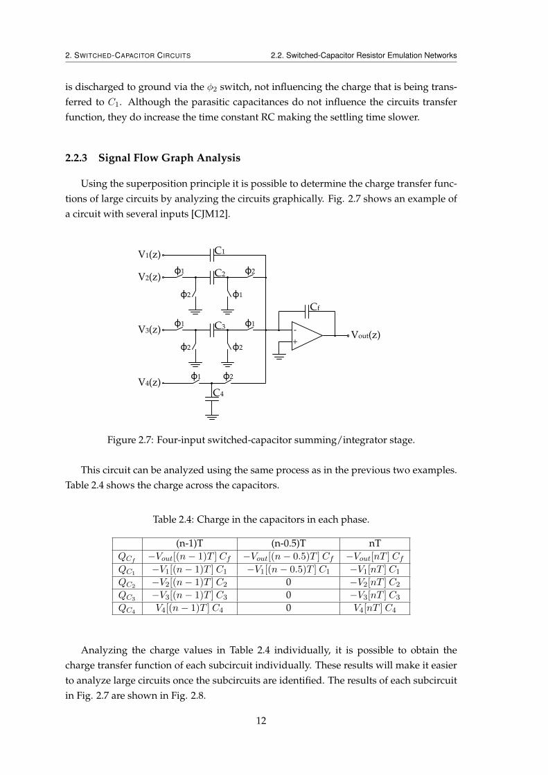
Using the superposition principle it is possible to determine the charge transfer func-tions of large circuits by analyzing the circuits graphically. Fig. 2.7 shows an example ofa circuit with several inputs [CJM12].
Vout(z)-
+
C4
φ1 φ2
Cf
C1
V2(z) C2φ1 φ2
φ2 φ1
V3(z) C3φ1 φ1
φ2 φ2
V4(z)
V1(z)
Figure 2.7: Four-input switched-capacitor summing/integrator stage.
This circuit can be analyzed using the same process as in the previous two examples.Table 2.4 shows the charge across the capacitors.
Table 2.4: Charge in the capacitors in each phase.
(n-1)T (n-0.5)T nTQCf
−Vout[(n− 1)T ] Cf −Vout[(n− 0.5)T ] Cf −Vout[nT ] Cf
QC1 −V1[(n− 1)T ] C1 −V1[(n− 0.5)T ] C1 −V1[nT ] C1
QC2 −V2[(n− 1)T ] C2 0 −V2[nT ] C2
QC3 −V3[(n− 1)T ] C3 0 −V3[nT ] C3
QC4 V4[(n− 1)T ] C4 0 V4[nT ] C4
Analyzing the charge values in Table 2.4 individually, it is possible to obtain thecharge transfer function of each subcircuit individually. These results will make it easierto analyze large circuits once the subcircuits are identified. The results of each subcircuitin Fig. 2.7 are shown in Fig. 2.8.
12
2. SWITCHED-CAPACITOR CIRCUITS 2.3. Sallen-Key Topology
-C1(1-z )V1(z)
-1
C2 zV2(z)
-1
-C3V3(z)
-C4 zV4(z)
-1
+. 1 .
Cf
. 1 .
1-z .
-1Vout(z)
Figure 2.8: Equivalent signal flow graph of Fig.2.7 circuit.
The signal flow graph (SFG) can be analyzed and the circuits transfer function is ob-tained.
Vout(z) = −C1
CfV1(z) +
C2
Cf
z−1
1− z−1V2(z)−
C3
Cf
1
1− z−1V3(z)−
C4
Cf
z−1
1− z−1V4(z) (2.13)
2.3 Sallen-Key Topology
The SC low-pass and band-pass filters implemented in this thesis are based on thecontinuous time Sallen-Key second-order filters. In this section these topologies are pre-sented and discussed.
2.3.1 Low-pass Sallen-Key Topology
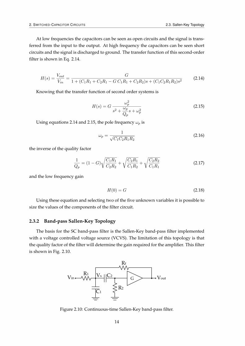
The basis for the SC low-pass filter is the Sallen-Key low-pass filter. This filter isshown in Fig. 2.9. One of the characteristics of this type of filter is the opamp beingconfigured as an amplifier instead of an integrator, reducing the gain-bandwidth re-quirements for the opamp. This means that when using this topology it is possible toimplement higher frequency filters with lower gain when compared to other topologies.Another advantage of this filter is the low ratio between largest and lowest resistor/ca-pacitor, which is an important for manufacturability.
VinR1 R2
C1
C2
VoutVx
G
Figure 2.9: Continuous-time Sallen-Key low-pass filter using an amplifier with gain G[SK55].
13
2. SWITCHED-CAPACITOR CIRCUITS 2.3. Sallen-Key Topology
At low frequencies the capacitors can be seen as open circuits and the signal is trans-ferred from the input to the output. At high frequency the capacitors can be seen shortcircuits and the signal is discharged to ground. The transfer function of this second-orderfilter is shown in Eq. 2.14.
H(s) =VoutVin
=G
1 + (C1R1 + C2R1 −GC1R1 + C2R2)s+ (C1C2R1R2)s2(2.14)
Knowing that the transfer function of second order systems is
H(s) = Gω2p
s2 +ωp
Qps+ ω2
p
(2.15)
Using equations 2.14 and 2.15, the pole frequency ωp is
ωp =1√
C1C2R1R2(2.16)
the inverse of the quality factor
1
Qp= (1−G)
√C1R1
C2R2+
√C2R1
C1R2+
√C2R2
C1R1(2.17)
and the low frequency gain
H(0) = G (2.18)
Using these equation and selecting two of the five unknown variables it is possible tosize the values of the components of the filter circuit.
2.3.2 Band-pass Sallen-Key Topology
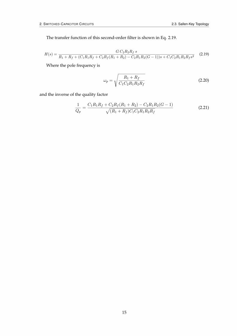
The basis for the SC band-pass filter is the Sallen-Key band-pass filter implementedwith a voltage controlled voltage source (VCVS). The limitation of this topology is thatthe quality factor of the filter will determine the gain required for the amplifier. This filteris shown in Fig. 2.10.
VinR1
R2
VoutVx
C1
C2
Rf
G
Figure 2.10: Continuous-time Sallen-Key band-pass filter.
14
2. SWITCHED-CAPACITOR CIRCUITS 2.3. Sallen-Key Topology
The transfer function of this second-order filter is shown in Eq. 2.19.
H(s) =GC2R2Rf s
R1 +Rf + (C1R1Rf + C2Rf (R1 +R2)− C2R1R2(G− 1))s+ C1C2R1R2Rfs2(2.19)
Where the pole frequency is
ωp =
√R1 +Rf
C1C2R1R2Rf(2.20)
and the inverse of the quality factor
1
Qp=C1R1Rf + C2Rf (R1 +R2)− C2R1R2(G− 1)√
(R1 +Rf )C1C2R1R2Rf
(2.21)
15
2. SWITCHED-CAPACITOR CIRCUITS 2.3. Sallen-Key Topology
16
3Low Pass Filter Topologies
3.1 Introduction
Low-pass filters are systems that allow the passing without attenuation of signalswith frequency below the cutoff frequency, while attenuating those with frequency aboveit. The amount of attenuation the signals with higher frequency suffer is dependent ontheir frequency and the order of the filter.
In this chapter low-pass SC filters based on the continuous-time version of the Sallen-Key low-pass filter [SK55] will be presented and discussed when using ideal components.Higher order low-pass SC filters using cascaded sections will also be discussed in thischapter.
3.2 Continuous-time Sallen-Key Low-Pass Filter
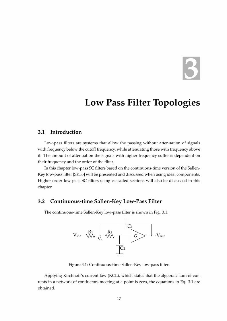
The continuous-time Sallen-Key low-pass filter is shown in Fig. 3.1.
VinR1 R2
C1
C2
VoutVx
G
Figure 3.1: Continuous-time Sallen-Key low-pass filter.
Applying Kirchhoff’s current law (KCL), which states that the algebraic sum of cur-rents in a network of conductors meeting at a point is zero, the equations in Eq. 3.1 areobtained.
17
3. LOW PASS FILTER TOPOLOGIES 3.3. Switched-Capacitor Low-Pass Filter
Vx − VinR1
+Vx − (1/G)Vout
R2+ (Vx − Vout) sC1 = 0
(1/G)Vout − VxR2
+ (1/G)Vout sC2 = 0
(3.1)
Combining both equations (Eq. 3.1) the filters transfer function is obtained. Thistransfer function (Eq. 3.2) shows that the Sallen-Key topology under consideration hereis a second-order low-pass filter.
H(s) =VoutVin
=G
1 + (C1R1 + C2R1 −GC1R1 + C2R2)s+ (C1C2R1R2)s2(3.2)
Several approximations can be used when designing filters. In this case the filterwill be designed using the Butterworth prototype transfer function which is described inAppendix A.1.
3.3 Switched-Capacitor Low-Pass Filter
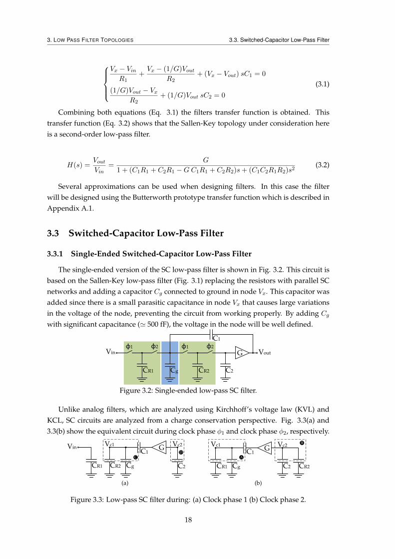
3.3.1 Single-Ended Switched-Capacitor Low-Pass Filter
The single-ended version of the SC low-pass filter is shown in Fig. 3.2. This circuit isbased on the Sallen-Key low-pass filter (Fig. 3.1) replacing the resistors with parallel SCnetworks and adding a capacitor Cg connected to ground in node Vx. This capacitor wasadded since there is a small parasitic capacitance in node Vx that causes large variationsin the voltage of the node, preventing the circuit from working properly. By adding Cg
with significant capacitance (' 500 fF), the voltage in the node will be well defined.
Vin Vout
Cg
Gφ1 φ2φ1 φ2
CR1 CR2 C2
C1
Figure 3.2: Single-ended low-pass SC filter.
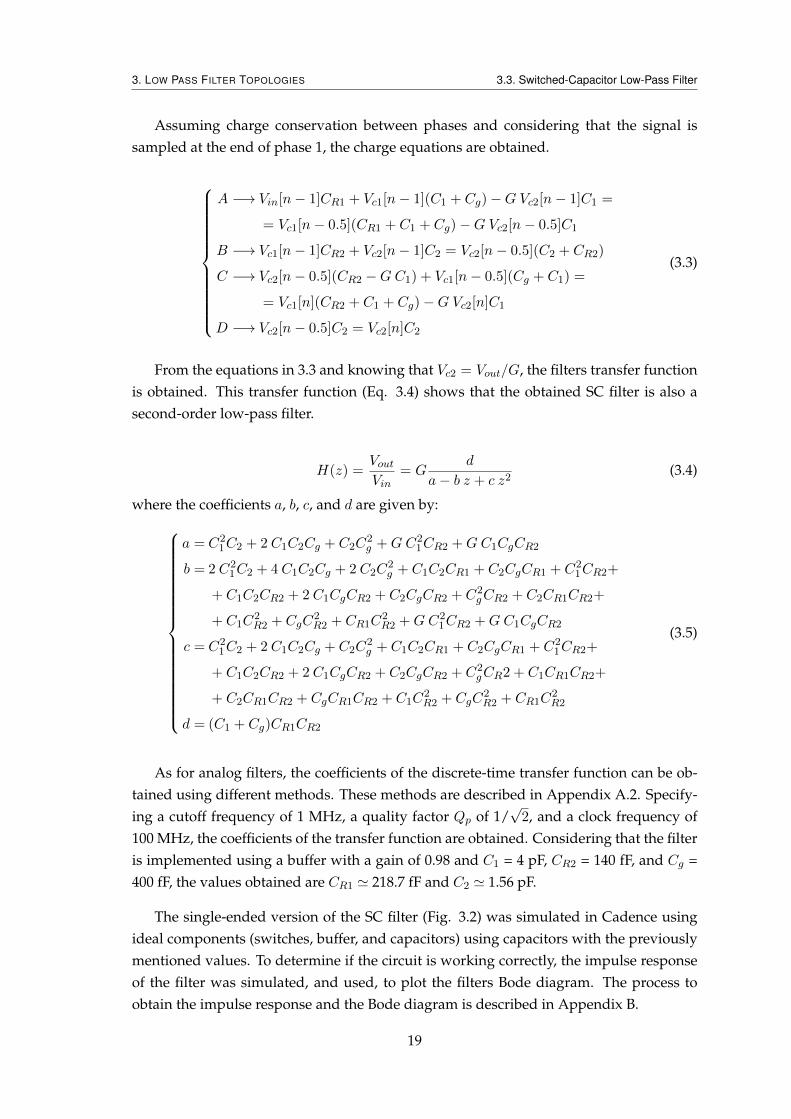
Unlike analog filters, which are analyzed using Kirchhoff’s voltage law (KVL) andKCL, SC circuits are analyzed from a charge conservation perspective. Fig. 3.3(a) and3.3(b) show the equivalent circuit during clock phase φ1 and clock phase φ2, respectively.
CgCR1 CR2
C1
C2
GVc1 Vc2Vin
C
D
(a)
CR1
Vc1 Vc2G
Cg C2 CR2
C1A
B
(b)
Figure 3.3: Low-pass SC filter during: (a) Clock phase 1 (b) Clock phase 2.
18
3. LOW PASS FILTER TOPOLOGIES 3.3. Switched-Capacitor Low-Pass Filter
Assuming charge conservation between phases and considering that the signal issampled at the end of phase 1, the charge equations are obtained.
A −→ Vin[n− 1]CR1 + Vc1[n− 1](C1 + Cg)−G Vc2[n− 1]C1 =
= Vc1[n− 0.5](CR1 + C1 + Cg)−G Vc2[n− 0.5]C1
B −→ Vc1[n− 1]CR2 + Vc2[n− 1]C2 = Vc2[n− 0.5](C2 + CR2)
C −→ Vc2[n− 0.5](CR2 −GC1) + Vc1[n− 0.5](Cg + C1) =
= Vc1[n](CR2 + C1 + Cg)−G Vc2[n]C1
D −→ Vc2[n− 0.5]C2 = Vc2[n]C2
(3.3)
From the equations in 3.3 and knowing that Vc2 = Vout/G, the filters transfer functionis obtained. This transfer function (Eq. 3.4) shows that the obtained SC filter is also asecond-order low-pass filter.
H(z) =VoutVin
= Gd
a− b z + c z2(3.4)
where the coefficients a, b, c, and d are given by:
a = C21C2 + 2 C1C2Cg + C2C
2g +GC2
1CR2 +GC1CgCR2
b = 2 C21C2 + 4 C1C2Cg + 2 C2C
2g + C1C2CR1 + C2CgCR1 + C2
1CR2+
+ C1C2CR2 + 2 C1CgCR2 + C2CgCR2 + C2gCR2 + C2CR1CR2+
+ C1C2R2 + CgC
2R2 + CR1C
2R2 +GC2
1CR2 +GC1CgCR2
c = C21C2 + 2 C1C2Cg + C2C
2g + C1C2CR1 + C2CgCR1 + C2
1CR2+
+ C1C2CR2 + 2 C1CgCR2 + C2CgCR2 + C2gCR2 + C1CR1CR2+
+ C2CR1CR2 + CgCR1CR2 + C1C2R2 + CgC
2R2 + CR1C
2R2
d = (C1 + Cg)CR1CR2
(3.5)
As for analog filters, the coefficients of the discrete-time transfer function can be ob-tained using different methods. These methods are described in Appendix A.2. Specify-ing a cutoff frequency of 1 MHz, a quality factor Qp of 1/
√2, and a clock frequency of
100 MHz, the coefficients of the transfer function are obtained. Considering that the filteris implemented using a buffer with a gain of 0.98 and C1 = 4 pF, CR2 = 140 fF, and Cg =400 fF, the values obtained are CR1 ' 218.7 fF and C2 ' 1.56 pF.
The single-ended version of the SC filter (Fig. 3.2) was simulated in Cadence usingideal components (switches, buffer, and capacitors) using capacitors with the previouslymentioned values. To determine if the circuit is working correctly, the impulse responseof the filter was simulated, and used, to plot the filters Bode diagram. The process toobtain the impulse response and the Bode diagram is described in Appendix B.
19
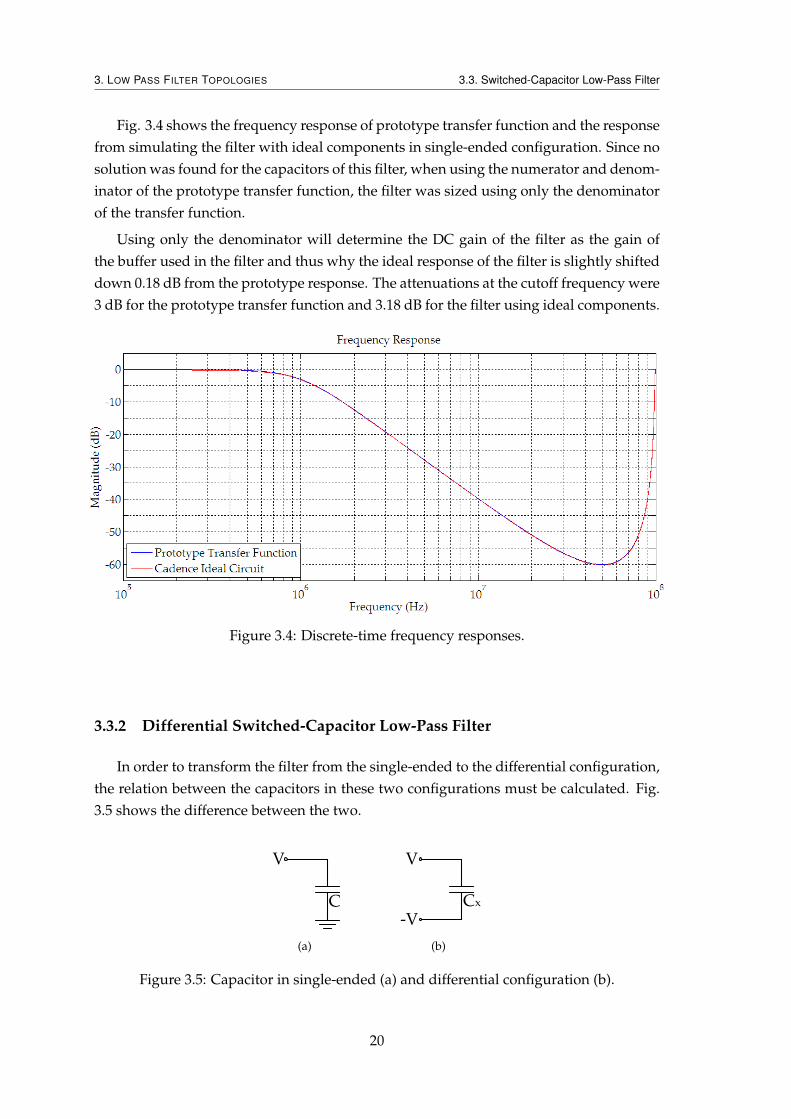
3. LOW PASS FILTER TOPOLOGIES 3.3. Switched-Capacitor Low-Pass Filter
Fig. 3.4 shows the frequency response of prototype transfer function and the responsefrom simulating the filter with ideal components in single-ended configuration. Since nosolution was found for the capacitors of this filter, when using the numerator and denom-inator of the prototype transfer function, the filter was sized using only the denominatorof the transfer function.
Using only the denominator will determine the DC gain of the filter as the gain ofthe buffer used in the filter and thus why the ideal response of the filter is slightly shifteddown 0.18 dB from the prototype response. The attenuations at the cutoff frequency were3 dB for the prototype transfer function and 3.18 dB for the filter using ideal components.
Figure 3.4: Discrete-time frequency responses.
3.3.2 Differential Switched-Capacitor Low-Pass Filter
In order to transform the filter from the single-ended to the differential configuration,the relation between the capacitors in these two configurations must be calculated. Fig.3.5 shows the difference between the two.
V
C
(a)
V
Cx
-V
(b)
Figure 3.5: Capacitor in single-ended (a) and differential configuration (b).
20
3. LOW PASS FILTER TOPOLOGIES 3.3. Switched-Capacitor Low-Pass Filter
Since the charge across the capacitor C is equal to C(V − 0) and the charge across Cx
is equal to Cx(V − (−V )), this means that the capacitor Cx must have half the capacitanceof C in order to store the same charge as capacitor C, assuming that V has the same valuein both cases. The differential configuration is shown in Fig. 3.6.
Vin
Cg
Cg
CR1/2 CR2/2 C2/2
C1
C1
Vip
φ1 φ2
φ1 φ2
φ1 φ2
φ1 φ2G
Figure 3.6: Differential low-pass SC filter.
The differential configuration of the SC filter was simulated and the frequency re-sponse was compared with the single-ended configuration (Fig. 3.7). This simulationshows that the relation between capacitance values in single-ended and differential con-figuration is correct.
Figure 3.7: Comparison between the frequency responses of the single-ended and differ-ential configurations.
21
3. LOW PASS FILTER TOPOLOGIES 3.4. Switched-Capacitor Filters Using Cascaded Sections
3.4 Switched-Capacitor Filters Using Cascaded Sections
Higher order SC filters can be obtained by cascading lower order filters. In this sec-tion a sixth-order low-pass filter will be built using three cascaded second-order sections,maintaining a 3 dB attenuation at the cutoff frequency.
In order to obtain this attenuation at the cutoff frequency, each of the second-ordersections must have a specific quality factor. Using Eq. A.2 with n = 6, the denominatorsfor the three second-order sections (Eq. 3.6) can be obtained.
T (S) =1
S2 + 0.5176S + 1
1
S2 + 1.4142S + 1
1
S2 + 1.9319S + 1(3.6)
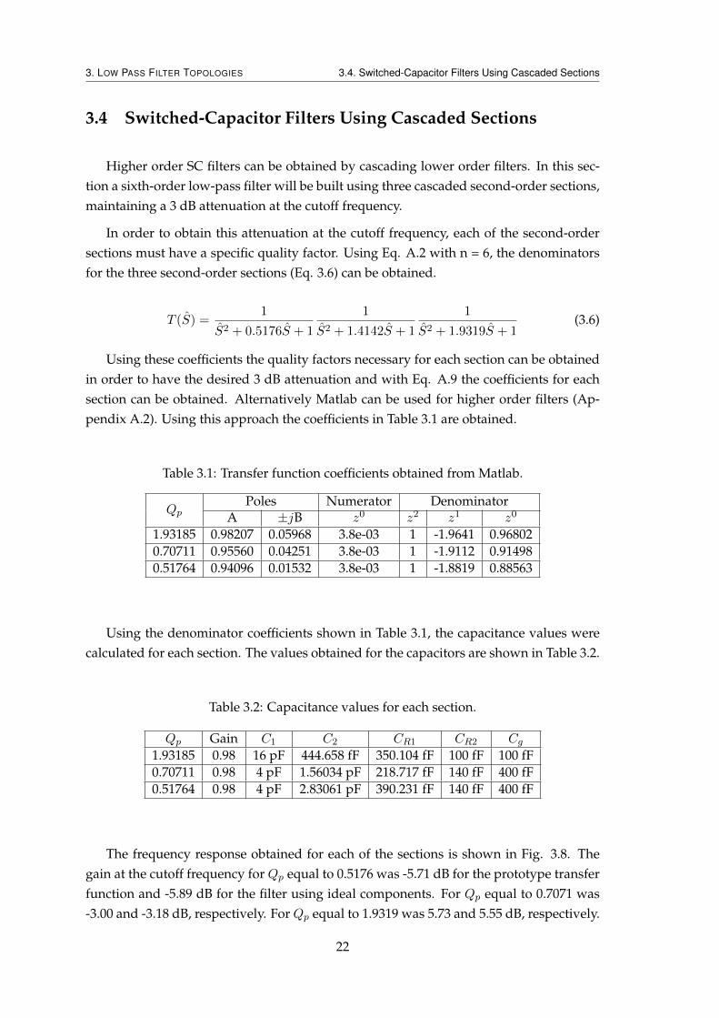
Using these coefficients the quality factors necessary for each section can be obtainedin order to have the desired 3 dB attenuation and with Eq. A.9 the coefficients for eachsection can be obtained. Alternatively Matlab can be used for higher order filters (Ap-pendix A.2). Using this approach the coefficients in Table 3.1 are obtained.
Table 3.1: Transfer function coefficients obtained from Matlab.
QpPoles Numerator Denominator
A ±jB z0 z2 z1 z0
1.93185 0.98207 0.05968 3.8e-03 1 -1.9641 0.968020.70711 0.95560 0.04251 3.8e-03 1 -1.9112 0.914980.51764 0.94096 0.01532 3.8e-03 1 -1.8819 0.88563
Using the denominator coefficients shown in Table 3.1, the capacitance values werecalculated for each section. The values obtained for the capacitors are shown in Table 3.2.
Table 3.2: Capacitance values for each section.
Qp Gain C1 C2 CR1 CR2 Cg
1.93185 0.98 16 pF 444.658 fF 350.104 fF 100 fF 100 fF0.70711 0.98 4 pF 1.56034 pF 218.717 fF 140 fF 400 fF0.51764 0.98 4 pF 2.83061 pF 390.231 fF 140 fF 400 fF
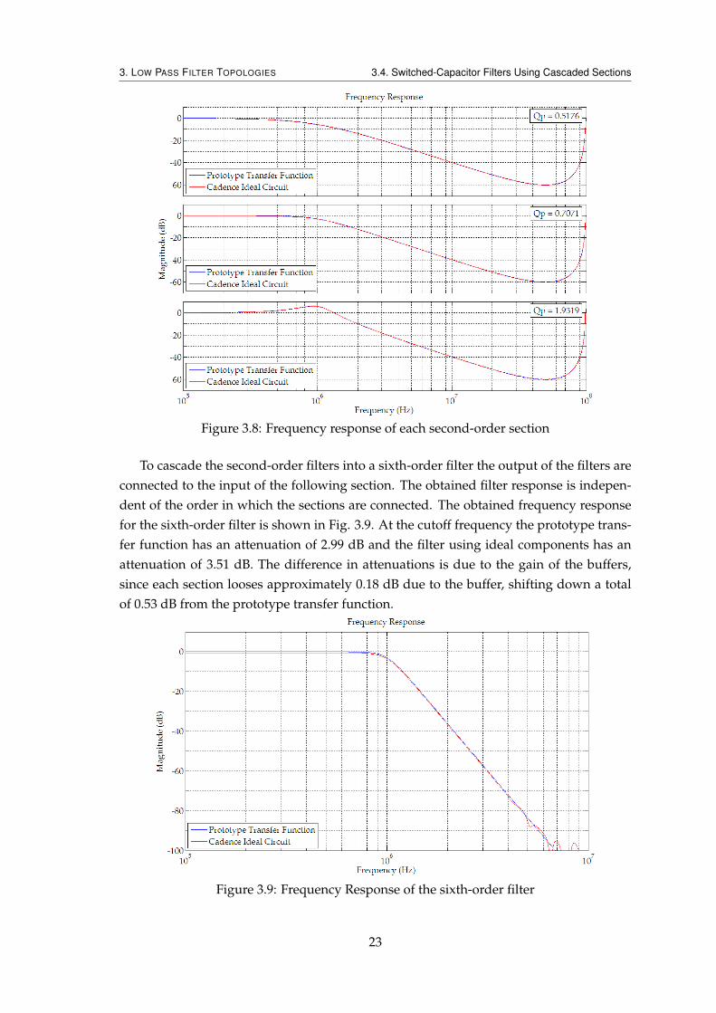
The frequency response obtained for each of the sections is shown in Fig. 3.8. Thegain at the cutoff frequency for Qp equal to 0.5176 was -5.71 dB for the prototype transferfunction and -5.89 dB for the filter using ideal components. For Qp equal to 0.7071 was-3.00 and -3.18 dB, respectively. For Qp equal to 1.9319 was 5.73 and 5.55 dB, respectively.
22
3. LOW PASS FILTER TOPOLOGIES 3.4. Switched-Capacitor Filters Using Cascaded Sections
Figure 3.8: Frequency response of each second-order section
To cascade the second-order filters into a sixth-order filter the output of the filters areconnected to the input of the following section. The obtained filter response is indepen-dent of the order in which the sections are connected. The obtained frequency responsefor the sixth-order filter is shown in Fig. 3.9. At the cutoff frequency the prototype trans-fer function has an attenuation of 2.99 dB and the filter using ideal components has anattenuation of 3.51 dB. The difference in attenuations is due to the gain of the buffers,since each section looses approximately 0.18 dB due to the buffer, shifting down a totalof 0.53 dB from the prototype transfer function.
Figure 3.9: Frequency Response of the sixth-order filter
23
3. LOW PASS FILTER TOPOLOGIES 3.5. Conclusions
3.5 Conclusions
This chapter presented from an ideal point of view that it is possible to implementlow-pass SC filters based on the Sallen-Key low-pass filter using near unity-gain buffers.It was also described how to obtain higher order filters based on second-order sectionswhile maintaining an attenuation of approximately -3 dB at the cutoff frequency. Thedifferences between the prototype transfer function frequency response and the idealcircuits response was due to the buffers gain. Since the filter was designed consideringonly the denominator of the prototype transfer function, the DC gain of the filter is equalto the buffers gain.
24
4Band Pass Filter Topologies
4.1 Introduction
Band-pass filters are systems that allow the passing of signals within a band of fre-quencies, while attenuating the frequencies outside the defined ranged. The amount ofattenuation the signals suffers outside the frequency range is dependent on the signalsfrequency and the order of the filter.
In this chapter band-pass SC filters based on the continuous-time version of the Sallen-Key band-pass filter implemented with a VCVS will be presented and discussed whenusing ideal components. Higher order band-pass SC filters using cascaded sections willalso be discussed in this chapter.
4.2 Continuous-time Sallen-Key Band-Pass Filter
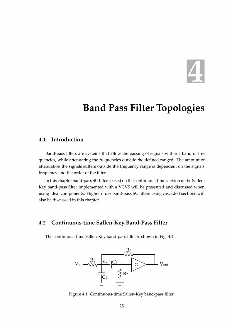
The continuous-time Sallen-Key band-pass filter is shown in Fig. 4.1.
VinR1
R2
VoutVx
C1
C2
Rf
G
Figure 4.1: Continuous-time Sallen-Key band-pass filter.
25
4. BAND PASS FILTER TOPOLOGIES 4.3. Switched-Capacitor Band-Pass Filter
Applying KCL to node Vx, the equations in Eq. 4.1 are obtained.Vx − VinR1
+Vx − Vout
Rf+ (Vx − (1/G)Vout) sC2 + Vx sC1 = 0
((1/G)Vout − Vx) sC2 +(1/G)Vout
R2= 0
(4.1)
Combining both equations (Eq. 4.1) the filters transfer function is obtained. Thistransfer function (Eq. 4.2) shows that the Sallen-Key topology under consideration hereis a second-order band-pass filter (one zero and two poles).
H(s) =GC2R2Rf s
Rf + C2R2Rf s+R1(1 + C1Rf s+ C2 s(R2 −GR2 +Rf + C1R2Rf s))(4.2)
Two methods to design a continuous-time band-pass filter using the Butterworth pro-totype transfer function is described in Appendix A.3.
4.3 Switched-Capacitor Band-Pass Filter
4.3.1 Single-Ended Switched-Capacitor Band-Pass Filter
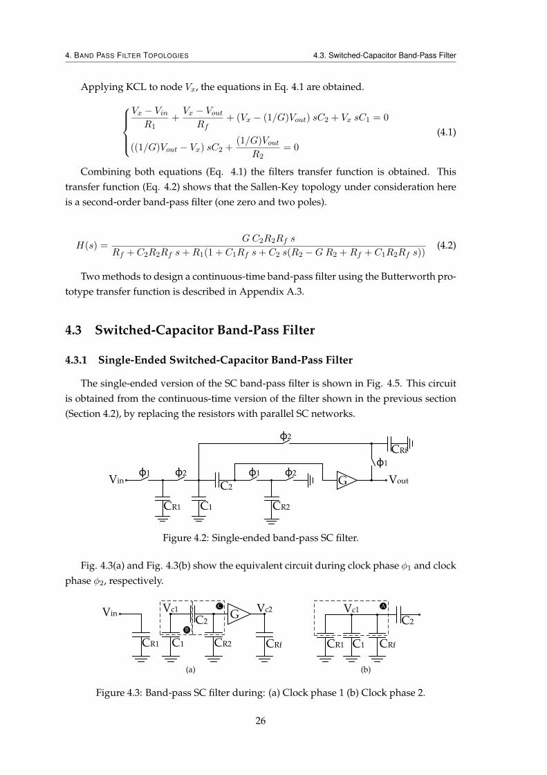
The single-ended version of the SC band-pass filter is shown in Fig. 4.5. This circuitis obtained from the continuous-time version of the filter shown in the previous section(Section 4.2), by replacing the resistors with parallel SC networks.
Vin Vout
CR1 C1
C2G
φ1 φ2
φ2
φ1
CRf
φ1 φ2
CR2
Figure 4.2: Single-ended band-pass SC filter.
Fig. 4.3(a) and Fig. 4.3(b) show the equivalent circuit during clock phase φ1 and clockphase φ2, respectively.
CR2CR1 C1
C2
CRf
GVc1 Vc2Vin
B
C
(a)
CR1
Vc1
C1
C2
A
CRf
(b)
Figure 4.3: Band-pass SC filter during: (a) Clock phase 1 (b) Clock phase 2.
26
4. BAND PASS FILTER TOPOLOGIES 4.3. Switched-Capacitor Band-Pass Filter
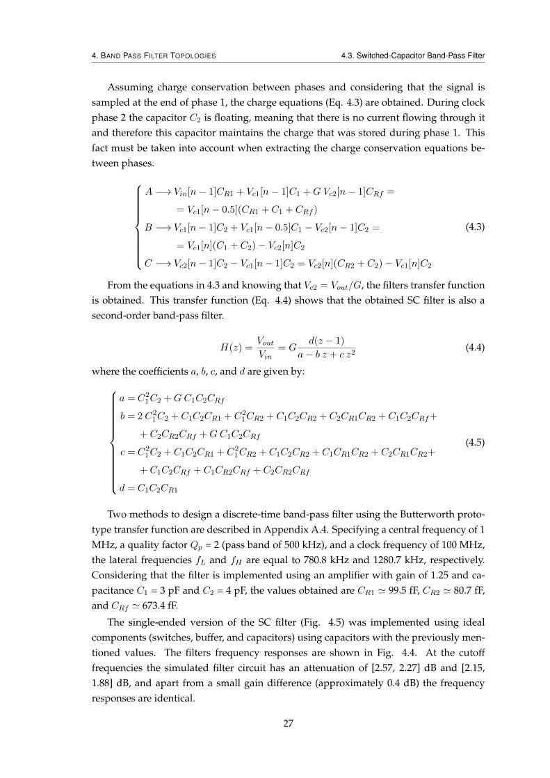
Assuming charge conservation between phases and considering that the signal issampled at the end of phase 1, the charge equations (Eq. 4.3) are obtained. During clockphase 2 the capacitor C2 is floating, meaning that there is no current flowing through itand therefore this capacitor maintains the charge that was stored during phase 1. Thisfact must be taken into account when extracting the charge conservation equations be-tween phases.
A −→ Vin[n− 1]CR1 + Vc1[n− 1]C1 +G Vc2[n− 1]CRf =
= Vc1[n− 0.5](CR1 + C1 + CRf )
B −→ Vc1[n− 1]C2 + Vc1[n− 0.5]C1 − Vc2[n− 1]C2 =
= Vc1[n](C1 + C2)− Vc2[n]C2
C −→ Vc2[n− 1]C2 − Vc1[n− 1]C2 = Vc2[n](CR2 + C2)− Vc1[n]C2
(4.3)
From the equations in 4.3 and knowing that Vc2 = Vout/G, the filters transfer functionis obtained. This transfer function (Eq. 4.4) shows that the obtained SC filter is also asecond-order band-pass filter.
H(z) =VoutVin
= Gd(z − 1)
a− b z + c z2(4.4)
where the coefficients a, b, c, and d are given by:
a = C21C2 +GC1C2CRf
b = 2 C21C2 + C1C2CR1 + C2
1CR2 + C1C2CR2 + C2CR1CR2 + C1C2CRf+
+ C2CR2CRf +GC1C2CRf
c = C21C2 + C1C2CR1 + C2
1CR2 + C1C2CR2 + C1CR1CR2 + C2CR1CR2+
+ C1C2CRf + C1CR2CRf + C2CR2CRf
d = C1C2CR1
(4.5)
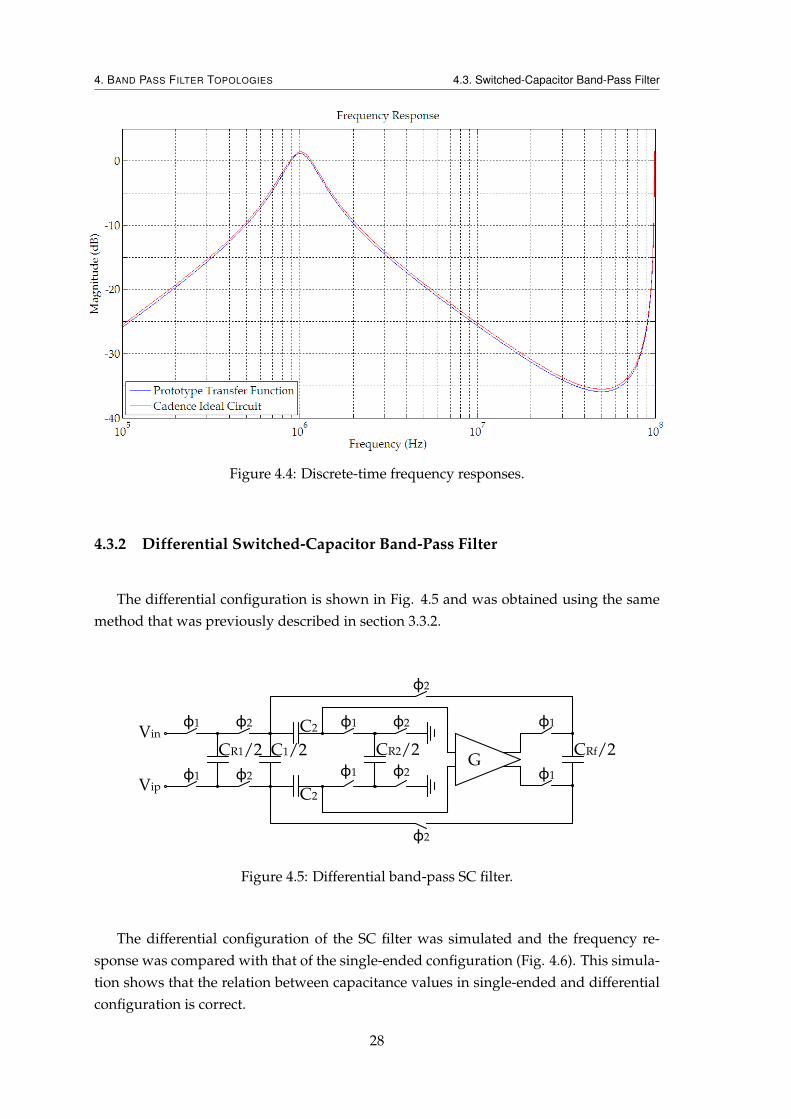
Two methods to design a discrete-time band-pass filter using the Butterworth proto-type transfer function are described in Appendix A.4. Specifying a central frequency of 1MHz, a quality factor Qp = 2 (pass band of 500 kHz), and a clock frequency of 100 MHz,the lateral frequencies fL and fH are equal to 780.8 kHz and 1280.7 kHz, respectively.Considering that the filter is implemented using an amplifier with gain of 1.25 and ca-pacitance C1 = 3 pF and C2 = 4 pF, the values obtained are CR1 ' 99.5 fF, CR2 ' 80.7 fF,and CRf ' 673.4 fF.
The single-ended version of the SC filter (Fig. 4.5) was implemented using idealcomponents (switches, buffer, and capacitors) using capacitors with the previously men-tioned values. The filters frequency responses are shown in Fig. 4.4. At the cutofffrequencies the simulated filter circuit has an attenuation of [2.57, 2.27] dB and [2.15,1.88] dB, and apart from a small gain difference (approximately 0.4 dB) the frequencyresponses are identical.
27
4. BAND PASS FILTER TOPOLOGIES 4.3. Switched-Capacitor Band-Pass Filter
Figure 4.4: Discrete-time frequency responses.
4.3.2 Differential Switched-Capacitor Band-Pass Filter
The differential configuration is shown in Fig. 4.5 and was obtained using the samemethod that was previously described in section 3.3.2.
Vin
CR1/2 C1/2
C2φ1 φ2
Vipφ1 φ2
CR2/2
C2
φ1 φ2
φ1 φ2
CRf/2
φ1
φ1
φ2
φ2
G
Figure 4.5: Differential band-pass SC filter.
The differential configuration of the SC filter was simulated and the frequency re-sponse was compared with that of the single-ended configuration (Fig. 4.6). This simula-tion shows that the relation between capacitance values in single-ended and differentialconfiguration is correct.
28
4. BAND PASS FILTER TOPOLOGIES 4.4. Switched-Capacitor Filters Using Cascaded Sections
Figure 4.6: Comparison between the frequency responses of the single-ended and differ-ential configurations.
4.4 Switched-Capacitor Filters Using Cascaded Sections
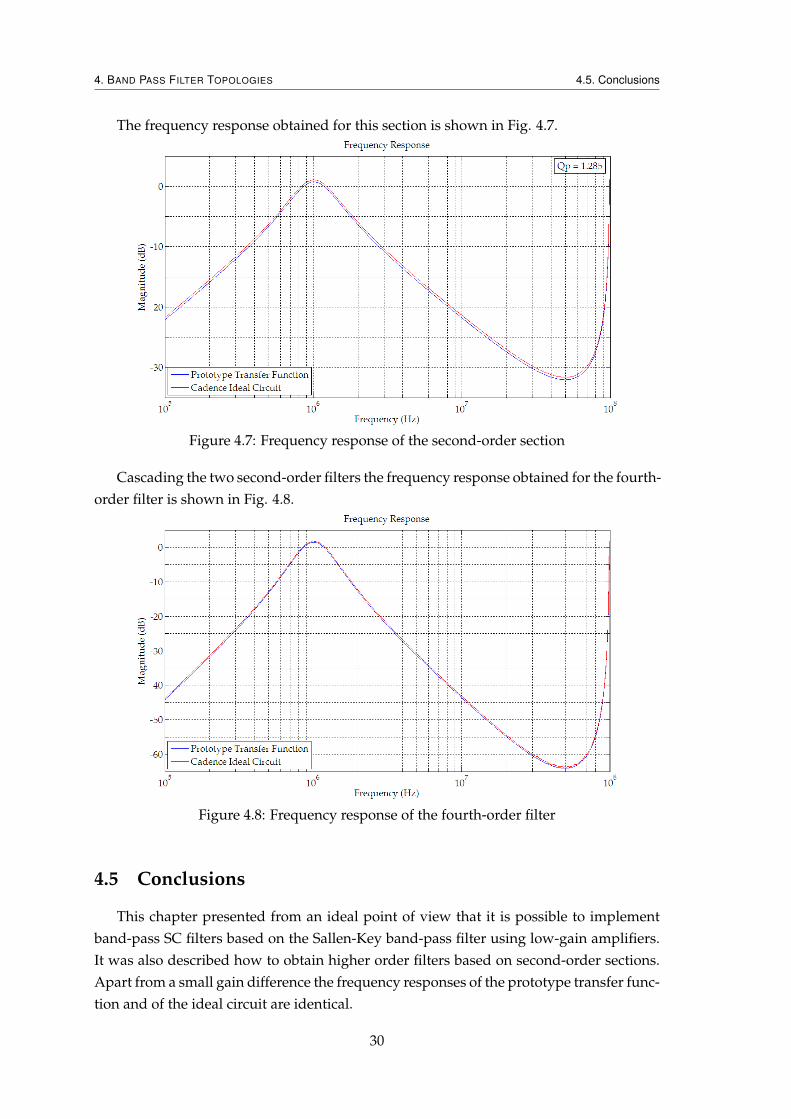
Higher order SC filters can be obtained by cascading lower order filters. In this sectiona fourth-order band-pass filter will be built using two cascaded second-order sectionswith the same quality factor (Qp = 1.285).
The coefficients for the cascaded second-order sections can be obtained using Eq. A.15with Qp = 1.285. This quality factor will define a 1.5 dB attenuation at the cutoff frequen-cies for each section and 3 dB for the cascaded section. Table 4.1 shows the poles locationand the transfer function coefficients.
Table 4.1: Transfer function coefficients obtained from the prototype method.
QpPoles Numerator Denominator
A ±jB z1 z0 z2 z1 z0
1.285 0.97555 0.05788 48.8964e-03 -48.8964e-03 1 -1.9511 0.95501
Using the denominator coefficients shown in Table 4.1, the capacitance values werecalculated for each section. The obtained values for the capacitors are shown in Table 4.2.
Table 4.2: Capacitance values for the cascaded sections.
Qp Gain C1 C2 CR1 CR2 CRf
1.285 1.25 3 pF 4 pF 154.535 fF 80.7119 fF 618.398 fF
29
4. BAND PASS FILTER TOPOLOGIES 4.5. Conclusions
The frequency response obtained for this section is shown in Fig. 4.7.
Figure 4.7: Frequency response of the second-order section
Cascading the two second-order filters the frequency response obtained for the fourth-order filter is shown in Fig. 4.8.
Figure 4.8: Frequency response of the fourth-order filter
4.5 Conclusions
This chapter presented from an ideal point of view that it is possible to implementband-pass SC filters based on the Sallen-Key band-pass filter using low-gain amplifiers.It was also described how to obtain higher order filters based on second-order sections.Apart from a small gain difference the frequency responses of the prototype transfer func-tion and of the ideal circuit are identical.
30
5Non-Ideal Effects
5.1 Introduction
In the previous two chapters the topologies of a low-pass and a band-pass filter havebeen presented using ideal components. In this chapter the non-ideal effects from usingreal components will be presented and discussed.
5.2 Non-linear effects due to real switches
Ideal switches have a very small constant resistance when they are closed, and a veryhigh constant resistance when they are open. Real switches (transistors), however, haveconsiderable resistance when they are closed and the value depends on the VGS voltageof the transistor, introducing distortion in the signal. Another source of distortion isthe parasitic capacitances of the real switch since their value also changes with the fournode voltages. In addition to the variation with the voltage, both the resistance and theparasitic capacitances change with the switches size. To determine the relation betweenthe non-linear effects of the switches and their sizes, a first-order low-pass SC filter will beanalyzed and simulated, since it’s a simple circuit with only two switches in single-endedconfiguration.
5.2.1 Filter Analysis
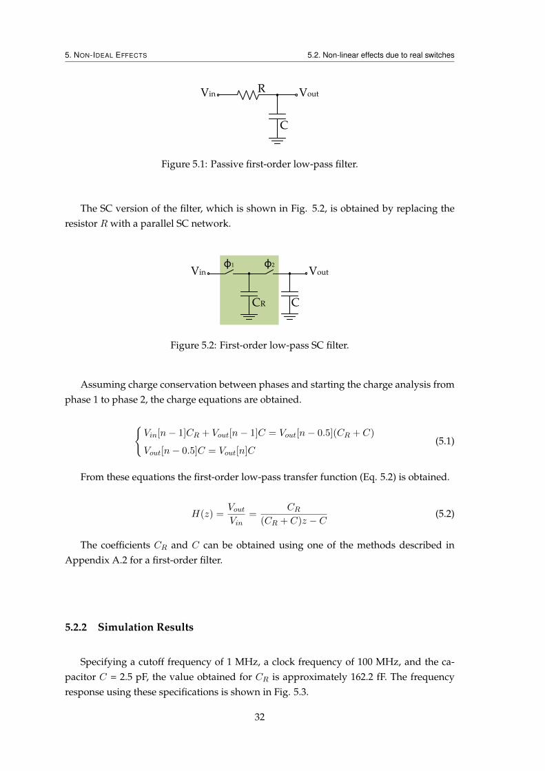
Fig. 5.1 shows a passive first-order low-pass filter from which the SC version is de-rived.
31
5. NON-IDEAL EFFECTS 5.2. Non-linear effects due to real switches
VinR
C
Vout
Figure 5.1: Passive first-order low-pass filter.
The SC version of the filter, which is shown in Fig. 5.2, is obtained by replacing theresistor R with a parallel SC network.
Vin Voutφ1 φ2
CCR
Figure 5.2: First-order low-pass SC filter.
Assuming charge conservation between phases and starting the charge analysis fromphase 1 to phase 2, the charge equations are obtained.
Vin[n− 1]CR + Vout[n− 1]C = Vout[n− 0.5](CR + C)
Vout[n− 0.5]C = Vout[n]C(5.1)
From these equations the first-order low-pass transfer function (Eq. 5.2) is obtained.
H(z) =VoutVin
=CR
(CR + C)z − C(5.2)
The coefficients CR and C can be obtained using one of the methods described inAppendix A.2 for a first-order filter.
5.2.2 Simulation Results
Specifying a cutoff frequency of 1 MHz, a clock frequency of 100 MHz, and the ca-pacitor C = 2.5 pF, the value obtained for CR is approximately 162.2 fF. The frequencyresponse using these specifications is shown in Fig. 5.3.
32
5. NON-IDEAL EFFECTS 5.2. Non-linear effects due to real switches
Figure 5.3: First-order filter frequency response.
To determine the influence of the non-linear effects of the resistance (1/gds) and theparasitic capacitances of the switches, the distortion of the filter was simulated usingthree versions of the SC filter (in differential configuration). In one version, the filter wassimulated using ideal switches. This simulation will give the best obtainable distortionsince it is not affected by the non-linear effects of switches and buffer. In the second ver-sion, the filter was simulated using a real switch. The distortion obtained from this sim-ulation is affected by the non-linear effects of both resistance and parasitic capacitances.In the third version, the filter was simulated using a real switch in parallel with an idealswitch. By doing this the non-linear effects due to the switches resistance are eliminatedsince the equivalent resistance of the switch is determined by the 1 Ω resistance of theideal switch. The distortion obtained from this simulation is then only affected by thenon-linear effects of the parasitic capacitances.
The simulation results are shown in Table 5.1 for three different switches, with a sinu-soidal differential signal with 600 mV of amplitude. In the transmission gate switch, thePMOS transistor is four times the size of the NMOS transistor to approximate the valuesof their resistance. All switches were simulated using minimum length (L = 120 nm).
Table 5.1: First-order filter distortions: Version 1 - NMOS switch driven by a 1.2 V clocksignal, Version 2 - NMOS switch driven by a clock boosted signal, Version 3 - Transmis-sion gate driven by 1.2 V clock signal.
THD (dB)Version Type of Switch W = 0.16 µm W = 1 µm W = 3 µm W = 7 µm W = 10 µm
1Ideal -105.02 -105.02 -102.90 -102.90 -103.01Real -15.70 -14.12 -15.53 -17.51 -18.69
Parallel -100.72 -96.70 -88.58 -82.39 -78.60
2Ideal -104.27 -104.27 -105.51 -105.51 -105.21Real -82.31 -64.20 -55.19 -50.28 -48.76
Parallel -100.26 -100.46 -76.41 -69.59 -70.19
3Ideal -103.13 -103.60 -103.54 -103.82 -103.43Real -60.25 -71.13 -64.44 -61.97 -60.89
Parallel -99.87 -92.27 -83.16 -75.88 -73.28
33
5. NON-IDEAL EFFECTS 5.2. Non-linear effects due to real switches
From Table 5.1 it can be concluded that when driven by a 1.2 V clock signal, theNMOS switch has very high distortion. The source of this distortion is the switches re-sistance that is very non-linear with the variation of the input voltage. In this case itcan be seen that the non-linear resistance dominates over the non-linear parasitic capac-itances. When driven by a clock boosted signal, the distortion introduced by the NMOSswitch decreases considerably. This is due to the decrease in the non-linear variation ofthe switches resistance with the input voltage, which will be seen later (Fig. 5.10). Thedistortion introduced by a transmission gate driven by a 1.2 V clock signal also decreases,but less than in the clock boosted NMOS switch.
Table 5.2 quantifies how much the non-linear effects of the MOS switches, i. e., thenon-linear resistance and the non-linear parasitic capacitances, increase the distortion ofthe SC circuit. The objective of this table is to clarify which non-linear effect dominatesthe overall distortion of the circuit when the width of the switches varies. The valuespresented in the table are calculated based on the distortion values presented on Table5.1 and represent the added distortion that each non-linear effect of the switch causes inthe circuit when compared to using ideal switches.
The added distortion of the parasitic capacitances is calculated subtracting the distor-tion of the ideal circuit from the distortion of the circuit with ideal switches in parallelwith real switches. The added distortion of the real switches (including both non-linearresistance and non-linear parasitic capacitances) is calculated subtracting the distortionof the ideal circuit from the distortion of the real circuit. Finally in order to better under-stand the dominant cause of distortion in the circuit, the difference between the distortionof the real circuit and the distortion of the circuit with the ideal switches in parallel withthe real switches is also calculated.
Table 5.2: Influence of the resistance and parasitic capacitances in the overall distortion:Version 1 - NMOS switch driven by a 1.2 V clock signal, Version 2 - NMOS switch drivenby a clock boosted signal, Version 3 - Transmission gate driven by 1.2 V clock signal.
Distortion (dB)Influence due to Version W = 0.16 µm W = 1 µm W = 3 µm W = 7 µm W = 10 µm
Parasitic capacitances1 4.3086 8.3282 14.3186 20.5033 24.41192 4.0116 3.8129 29.0997 35.9156 35.01813 3.2598 11.3249 20.3846 27.9446 30.1463
Parasitic capacitances 1 89.3278 90.9076 87.3650 85.3835 84.3211and 2 21.9645 40.0682 50.3245 55.2281 56.4415
resistance 3 42.8830 32.4657 39.0956 41.8570 42.5393
Resistance1 85.0192 82.5794 73.0464 64.8802 59.90922 17.9529 36.2553 21.2247 19.3125 21.42353 39.6232 21.1408 18.7110 13.9124 12.3931
From Table 5.2 it can be seen that the distortion introduced by the parasitic capaci-tances increases with the size of the switch, which means that the non-linearity of thesecapacitances increases with the width of the transistor and will become harder to com-pensate their effect in larger switches. As for the switches resistance, its non-linearity
34
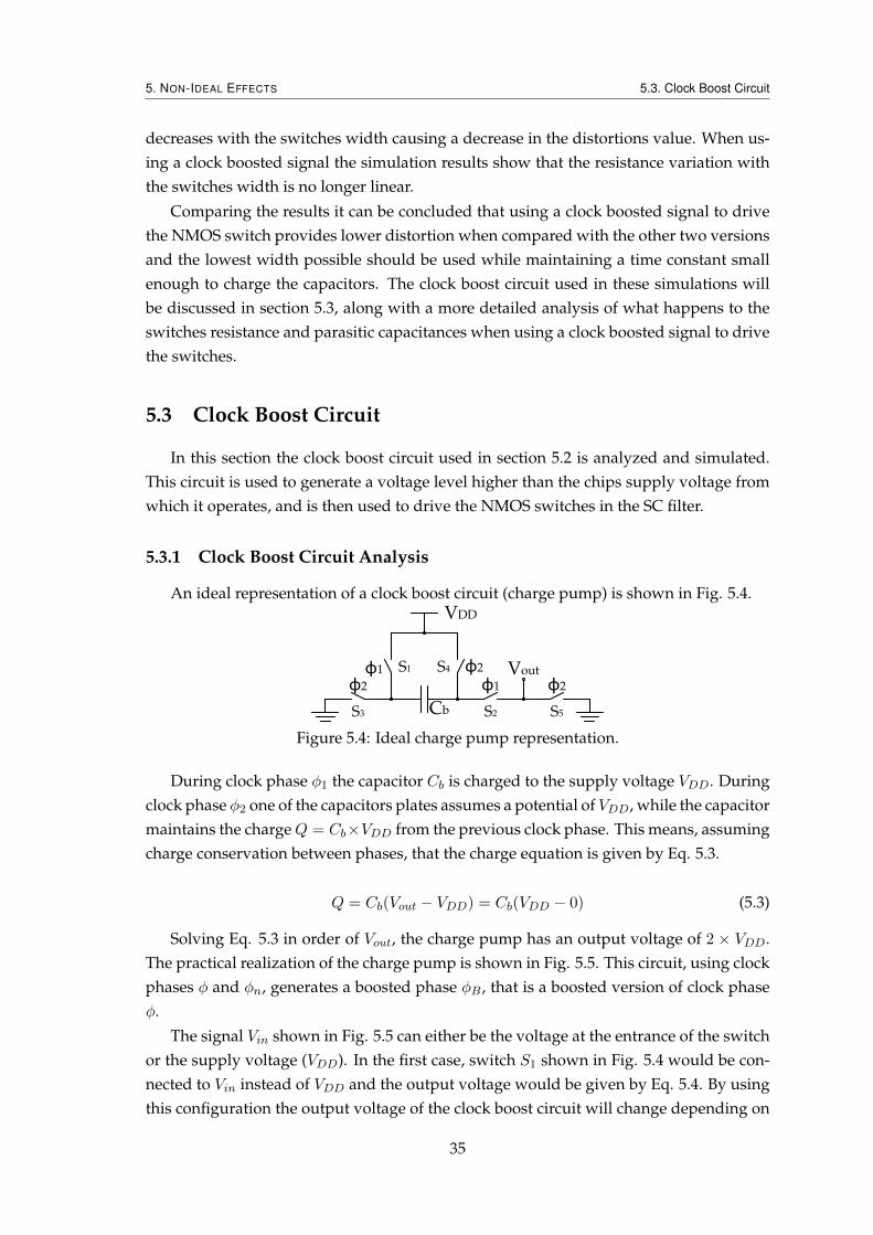
5. NON-IDEAL EFFECTS 5.3. Clock Boost Circuit
decreases with the switches width causing a decrease in the distortions value. When us-ing a clock boosted signal the simulation results show that the resistance variation withthe switches width is no longer linear.
Comparing the results it can be concluded that using a clock boosted signal to drivethe NMOS switch provides lower distortion when compared with the other two versionsand the lowest width possible should be used while maintaining a time constant smallenough to charge the capacitors. The clock boost circuit used in these simulations willbe discussed in section 5.3, along with a more detailed analysis of what happens to theswitches resistance and parasitic capacitances when using a clock boosted signal to drivethe switches.
5.3 Clock Boost Circuit
In this section the clock boost circuit used in section 5.2 is analyzed and simulated.This circuit is used to generate a voltage level higher than the chips supply voltage fromwhich it operates, and is then used to drive the NMOS switches in the SC filter.
5.3.1 Clock Boost Circuit Analysis
An ideal representation of a clock boost circuit (charge pump) is shown in Fig. 5.4.
Cb
VDD
φ1
φ1
φ2S1 S4
S2
φ2
S3
Vout
φ2
S5
Figure 5.4: Ideal charge pump representation.
During clock phase φ1 the capacitor Cb is charged to the supply voltage VDD. Duringclock phase φ2 one of the capacitors plates assumes a potential of VDD, while the capacitormaintains the chargeQ = Cb×VDD from the previous clock phase. This means, assumingcharge conservation between phases, that the charge equation is given by Eq. 5.3.
Q = Cb(Vout − VDD) = Cb(VDD − 0) (5.3)
Solving Eq. 5.3 in order of Vout, the charge pump has an output voltage of 2 × VDD.The practical realization of the charge pump is shown in Fig. 5.5. This circuit, using clockphases φ and φn, generates a boosted phase φB , that is a boosted version of clock phaseφ.
The signal Vin shown in Fig. 5.5 can either be the voltage at the entrance of the switchor the supply voltage (VDD). In the first case, switch S1 shown in Fig. 5.4 would be con-nected to Vin instead of VDD and the output voltage would be given by Eq. 5.4. By usingthis configuration the output voltage of the clock boost circuit will change depending on
35
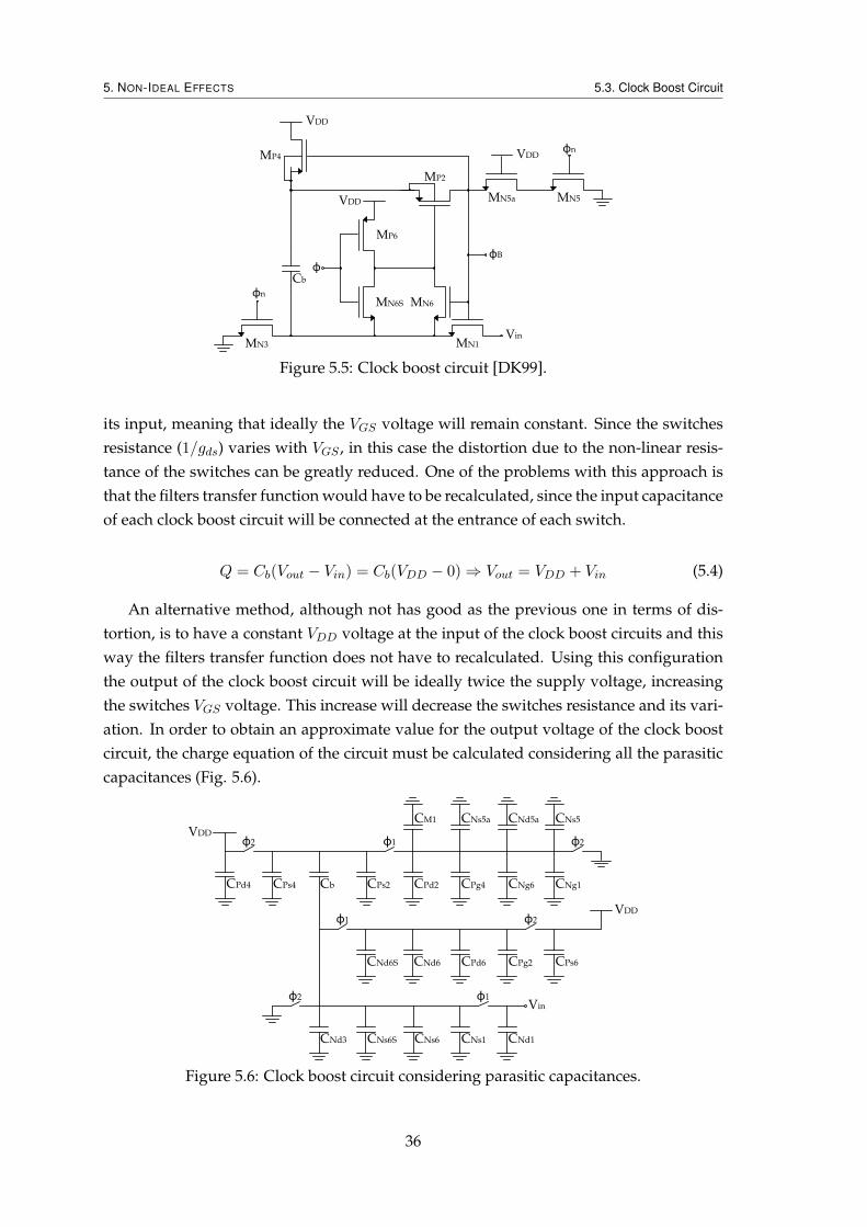
5. NON-IDEAL EFFECTS 5.3. Clock Boost Circuit
φ
φn
Vin
VDD
VDD
VDD
Cb
MN5a MN5
MN1
MN6S MN6
MP6
MP2
MP4
φB
φn
MN3
Figure 5.5: Clock boost circuit [DK99].
its input, meaning that ideally the VGS voltage will remain constant. Since the switchesresistance (1/gds) varies with VGS , in this case the distortion due to the non-linear resis-tance of the switches can be greatly reduced. One of the problems with this approach isthat the filters transfer function would have to be recalculated, since the input capacitanceof each clock boost circuit will be connected at the entrance of each switch.
Q = Cb(Vout − Vin) = Cb(VDD − 0)⇒ Vout = VDD + Vin (5.4)
An alternative method, although not has good as the previous one in terms of dis-tortion, is to have a constant VDD voltage at the input of the clock boost circuits and thisway the filters transfer function does not have to recalculated. Using this configurationthe output of the clock boost circuit will be ideally twice the supply voltage, increasingthe switches VGS voltage. This increase will decrease the switches resistance and its vari-ation. In order to obtain an approximate value for the output voltage of the clock boostcircuit, the charge equation of the circuit must be calculated considering all the parasiticcapacitances (Fig. 5.6).
VDD
CPd4 CPs4 Cb CPs2 CPd2 CPg4 CNg6 CNg1
CM1 CNs5a CNd5a CNs5
CNd6S CNd6 CPd6 CPg2
VDD
CPs6
CNd3 CNs6S CNs6 CNs1 CNd1
Vin
φ2 φ1 φ2
φ1 φ2
φ2 φ1
Figure 5.6: Clock boost circuit considering parasitic capacitances.
36
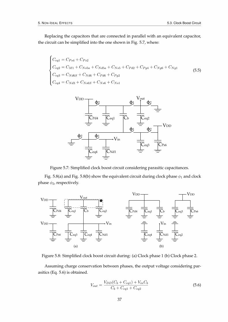
5. NON-IDEAL EFFECTS 5.3. Clock Boost Circuit
Replacing the capacitors that are connected in parallel with an equivalent capacitor,the circuit can be simplified into the one shown in Fig. 5.7, where:
Ceq1 = CPs4 + CPs2
Ceq2 = CM1 + CNs5a + CNd5a + CNs5 + CPd2 + CPg4 + CNg6 + CNg1
Ceq3 = CNd6S + CNd6 + CPd6 + CPg2
Ceq4 = CNd3 + CNs6S + CNs6 + CNs1
(5.5)
VDD
CPd4 Ceq1 Cb Ceq2
Ceq3
VDD
CPs6
Ceq4 CNd1
Vin
φ2 φ1 φ2
φ1 φ2
φ2 φ1
Vout
Figure 5.7: Simplified clock boost circuit considering parasitic capacitances.
Fig. 5.8(a) and Fig. 5.8(b) show the equivalent circuit during clock phase φ1 and clockphase φ2, respectively.
VDD
CPd4 Ceq1 Cb Ceq2
VDD
CPs6 Ceq4 CNd1
Vin
Vout
Ceq3
1
(a)
VDD
CPd4 Ceq1 Cb
Ceq2
Ceq3
VDD
CPs6
Ceq4 CNd1
Vin
(b)
Figure 5.8: Simplified clock boost circuit during: (a) Clock phase 1 (b) Clock phase 2.
Assuming charge conservation between phases, the output voltage considering par-asitics (Eq. 5.6) is obtained.
Vout =VDD(Cb + Ceq1) + VinCb
Cb + Ceq1 + Ceq2(5.6)
37
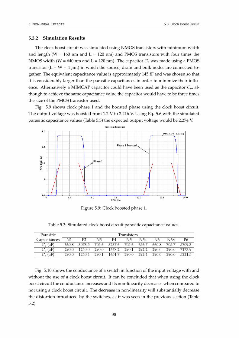
5. NON-IDEAL EFFECTS 5.3. Clock Boost Circuit
5.3.2 Simulation Results
The clock boost circuit was simulated using NMOS transistors with minimum widthand length (W = 160 nm and L = 120 nm) and PMOS transistors with four times theNMOS width (W = 640 nm and L = 120 nm). The capacitor Cb was made using a PMOStransistor (L = W = 4 µm) in which the source, drain and bulk nodes are connected to-gether. The equivalent capacitance value is approximately 145 fF and was chosen so thatit is considerably larger than the parasitic capacitances in order to minimize their influ-ence. Alternatively a MIMCAP capacitor could have been used as the capacitor Cb, al-though to achieve the same capacitance value the capacitor would have to be three timesthe size of the PMOS transistor used.
Fig. 5.9 shows clock phase 1 and the boosted phase using the clock boost circuit.The output voltage was boosted from 1.2 V to 2.216 V. Using Eq. 5.6 with the simulatedparasitic capacitance values (Table 5.3) the expected output voltage would be 2.274 V.
Phase 1
Phase 1 Boosted
Figure 5.9: Clock boosted phase 1.
Table 5.3: Simulated clock boost circuit parasitic capacitance values.
Parasitic TransistorsCapacitances N1 P2 N3 P4 N5 N5a N6 N6S P6
Cg (aF) 660.8 3073.5 705.6 3237.6 705.6 656.7 660.8 705.7 5709.3Cd (aF) 290.0 1240.0 290.0 1578.2 290.1 292.2 290.0 290.0 7173.9Cs (aF) 290.0 1240.4 290.1 1651.7 290.0 292.4 290.0 290.0 5221.5
Fig. 5.10 shows the conductance of a switch in function of the input voltage with andwithout the use of a clock boost circuit. It can be concluded that when using the clockboost circuit the conductance increases and its non-linearity decreases when compared tonot using a clock boost circuit. The decrease in non-linearity will substantially decreasethe distortion introduced by the switches, as it was seen in the previous section (Table5.2).
38
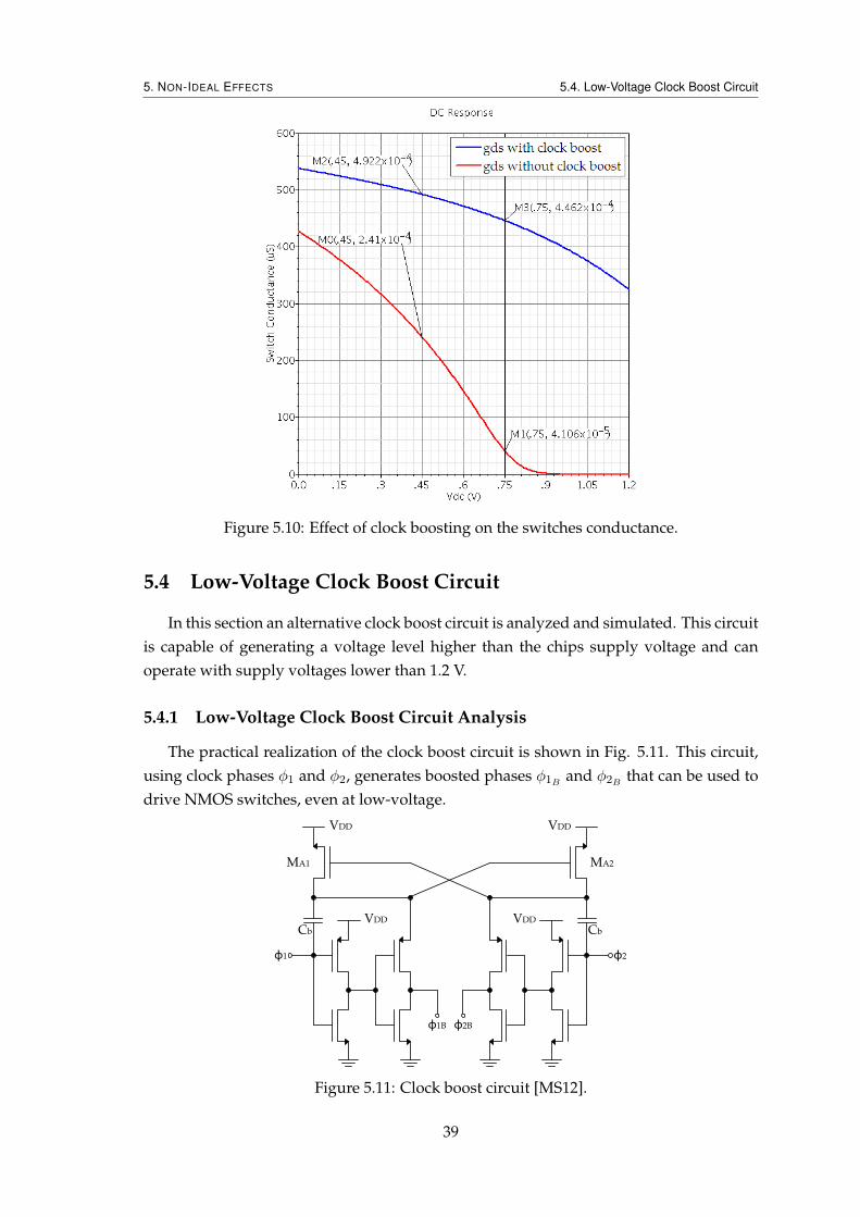
5. NON-IDEAL EFFECTS 5.4. Low-Voltage Clock Boost Circuit
Figure 5.10: Effect of clock boosting on the switches conductance.
5.4 Low-Voltage Clock Boost Circuit
In this section an alternative clock boost circuit is analyzed and simulated. This circuitis capable of generating a voltage level higher than the chips supply voltage and canoperate with supply voltages lower than 1.2 V.
5.4.1 Low-Voltage Clock Boost Circuit Analysis
The practical realization of the clock boost circuit is shown in Fig. 5.11. This circuit,using clock phases φ1 and φ2, generates boosted phases φ1B and φ2B that can be used todrive NMOS switches, even at low-voltage.
φ1
φ1B
Cb
VDD
MA1
VDD
φ2
φ2B
Cb
VDD
MA2
VDD
Figure 5.11: Clock boost circuit [MS12].
39
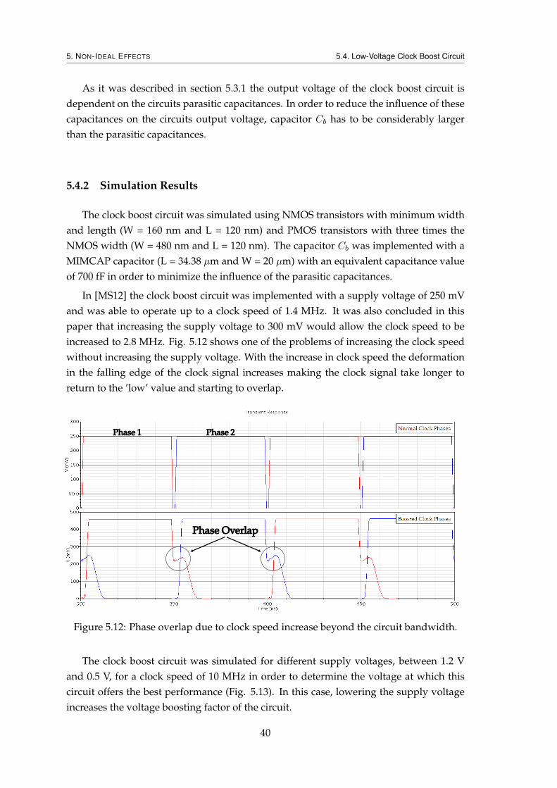
5. NON-IDEAL EFFECTS 5.4. Low-Voltage Clock Boost Circuit
As it was described in section 5.3.1 the output voltage of the clock boost circuit isdependent on the circuits parasitic capacitances. In order to reduce the influence of thesecapacitances on the circuits output voltage, capacitor Cb has to be considerably largerthan the parasitic capacitances.
5.4.2 Simulation Results
The clock boost circuit was simulated using NMOS transistors with minimum widthand length (W = 160 nm and L = 120 nm) and PMOS transistors with three times theNMOS width (W = 480 nm and L = 120 nm). The capacitor Cb was implemented with aMIMCAP capacitor (L = 34.38 µm and W = 20 µm) with an equivalent capacitance valueof 700 fF in order to minimize the influence of the parasitic capacitances.
In [MS12] the clock boost circuit was implemented with a supply voltage of 250 mVand was able to operate up to a clock speed of 1.4 MHz. It was also concluded in thispaper that increasing the supply voltage to 300 mV would allow the clock speed to beincreased to 2.8 MHz. Fig. 5.12 shows one of the problems of increasing the clock speedwithout increasing the supply voltage. With the increase in clock speed the deformationin the falling edge of the clock signal increases making the clock signal take longer toreturn to the ’low’ value and starting to overlap.
Phase Overlap
Phase 1 Phase 2
Figure 5.12: Phase overlap due to clock speed increase beyond the circuit bandwidth.
The clock boost circuit was simulated for different supply voltages, between 1.2 Vand 0.5 V, for a clock speed of 10 MHz in order to determine the voltage at which thiscircuit offers the best performance (Fig. 5.13). In this case, lowering the supply voltageincreases the voltage boosting factor of the circuit.
40
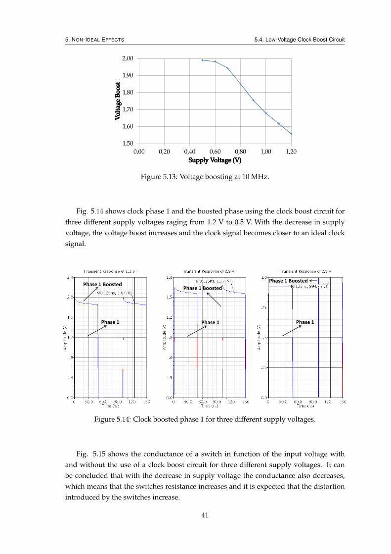
5. NON-IDEAL EFFECTS 5.4. Low-Voltage Clock Boost Circuit
1,50
1,60
1,70
1,80
1,90
2,00
0,00 0,20 0,40 0,60 0,80 1,00 1,20
Vo
ltag
e B
oo
st
Supply Voltage (V)
Figure 5.13: Voltage boosting at 10 MHz.
Fig. 5.14 shows clock phase 1 and the boosted phase using the clock boost circuit forthree different supply voltages raging from 1.2 V to 0.5 V. With the decrease in supplyvoltage, the voltage boost increases and the clock signal becomes closer to an ideal clocksignal.
Phase 1
Phase 1 Boosted
Phase 1
Phase 1 Boosted
Phase 1
Phase 1 Boosted
Figure 5.14: Clock boosted phase 1 for three different supply voltages.
Fig. 5.15 shows the conductance of a switch in function of the input voltage withand without the use of a clock boost circuit for three different supply voltages. It canbe concluded that with the decrease in supply voltage the conductance also decreases,which means that the switches resistance increases and it is expected that the distortionintroduced by the switches increase.
41
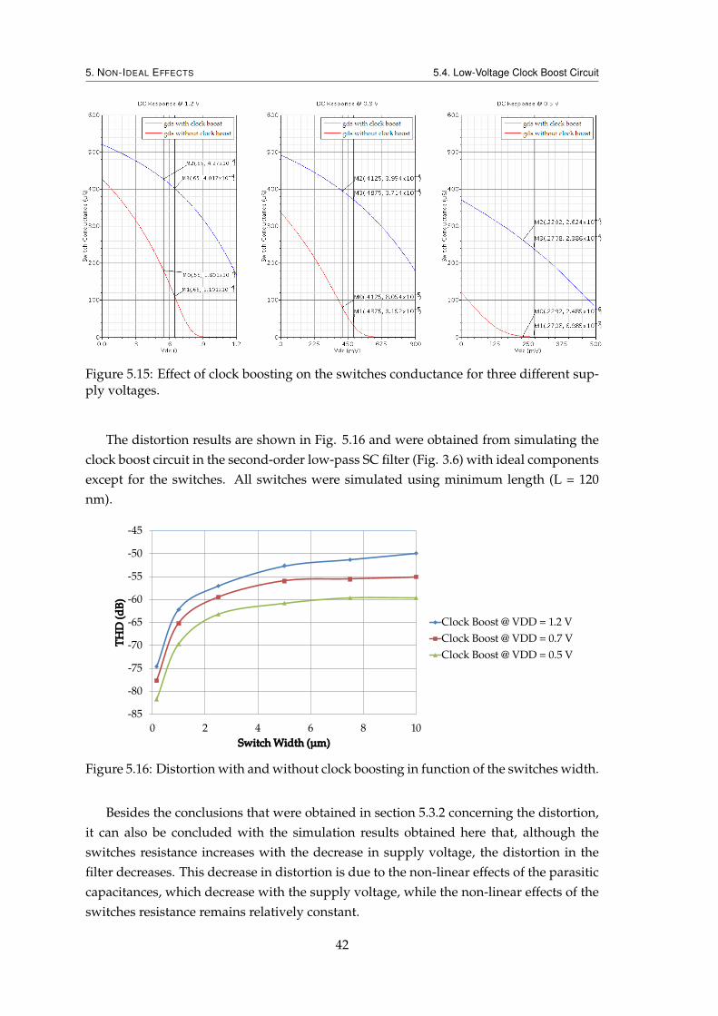
5. NON-IDEAL EFFECTS 5.4. Low-Voltage Clock Boost Circuit
Figure 5.15: Effect of clock boosting on the switches conductance for three different sup-ply voltages.
The distortion results are shown in Fig. 5.16 and were obtained from simulating theclock boost circuit in the second-order low-pass SC filter (Fig. 3.6) with ideal componentsexcept for the switches. All switches were simulated using minimum length (L = 120nm).
-85
-80
-75
-70
-65
-60
-55
-50
-45
0 2 4 6 8 10
TH
D (
dB
)
Switch Width (µm)
Clock Boost @ VDD = 1.2 V
Clock Boost @ VDD = 0.7 V
Clock Boost @ VDD = 0.5 V
Figure 5.16: Distortion with and without clock boosting in function of the switches width.
Besides the conclusions that were obtained in section 5.3.2 concerning the distortion,it can also be concluded with the simulation results obtained here that, although theswitches resistance increases with the decrease in supply voltage, the distortion in thefilter decreases. This decrease in distortion is due to the non-linear effects of the parasiticcapacitances, which decrease with the supply voltage, while the non-linear effects of theswitches resistance remains relatively constant.
42
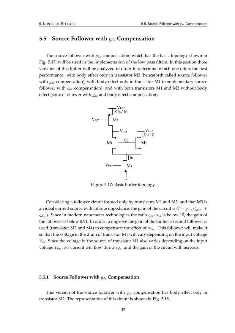
5. NON-IDEAL EFFECTS 5.5. Source Follower with gds Compensation
5.5 Source Follower with gds Compensation
The source follower with gds compensation, which has the basic topology shown inFig. 5.17, will be used in the implementation of the low pass filters. In this section threeversions of this buffer will be analyzed in order to determine which one offers the bestperformance: with body effect only in transistor M2 (henceforth called source followerwith gds compensation), with body effect only in transistor M1 (complementary sourcefollower with gds compensation), and with both transistors M1 and M2 without bodyeffect (source follower with gds and body effect compensation).
M3
M1 M2
M4
9IB/10
Vin
Vbp
Vout
VDD
VDD
Vbn
IB/10
IB
Figure 5.17: Basic buffer topology.
Considering a follower circuit formed only by transistors M1 and M3, and that M3 isan ideal current source with infinite impedance, the gain of the circuit is G = gm1/(gm1 +
gds1). Since in modern nanometer technologies the ratio gm/gds is below 10, the gain ofthe follower is below 0.91. In order to improve the gain of the buffer, a second follower isused (transistor M2 and M4) to compensate the effect of gds1 . This follower will make itso that the voltage in the drain of transistor M1 will vary depending on the input voltageVin. Since the voltage in the source of transistor M1 also varies depending on the inputvoltage Vin, less current will flow throw rds1 and the gain of the circuit will increase.
5.5.1 Source Follower with gds Compensation
This version of the source follower with gds compensation has body effect only intransistor M2. The representation of this circuit is shown in Fig. 5.18.
43
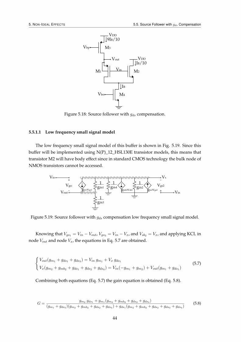
5. NON-IDEAL EFFECTS 5.5. Source Follower with gds Compensation
M3
M1 M2
M4
9IB/10
Vin
Vbp
Vout
VDD
VDD
Vbn
IB/10
IB
Figure 5.18: Source follower with gds compensation.
5.5.1.1 Low frequency small signal model
The low frequency small signal model of this buffer is shown in Fig. 5.19. Since thisbuffer will be implemented using N(P)_12_HSL130E transistor models, this means thattransistor M2 will have body effect since in standard CMOS technology the bulk node ofNMOS transistors cannot be accessed.
Vin Vx
gmb2vsb2 gm2vgs2
Vout Vin
1 .
gds1
1 .
gds3
1 .
gds2gm1vgs1
1 .
gds4
+
-
Vgs1
-
+
Vgs2
Figure 5.19: Source follower with gds compensation low frequency small signal model.
Knowing that Vgs1 = Vin − Vout, Vgs2 = Vin − Vx, and Vsb2 = Vx, and applying KCL innode Vout and node Vx, the equations in Eq. 5.7 are obtained.
Vout(gm1 + gds1 + gds3) = Vin gm1 + Vx gds1
Vx(gm2 + gmb2 + gds1 + gds2 + gds4) = Vin(−gm1 + gm2) + Vout(gm1 + gds1)(5.7)
Combining both equations (Eq. 5.7) the gain equation is obtained (Eq. 5.8).
G =gm2
gds1 + gm1(gm2
+ gmb2 + gds2 + gds4)
(gm1 + gds3)(gm2 + gmb2 + gds2 + gds4) + gds1(gm2 + gmb2 + gds2 + gds3 + gds4)(5.8)
44
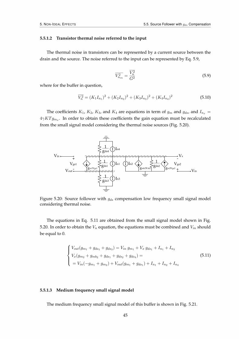
5. NON-IDEAL EFFECTS 5.5. Source Follower with gds Compensation
5.5.1.2 Transistor thermal noise referred to the input
The thermal noise in transistors can be represented by a current source between thedrain and the source. The noise referred to the input can be represented by Eq. 5.9,
V 2nin
=V 2n
G2(5.9)
where for the buffer in question,
V 2n = (K1In1)2 + (K2In2)2 + (K3In3)2 + (K4In4)2 (5.10)
The coefficients K1, K2, K3, and K4 are equations in term of gm and gds, and Inx =
4γKTgmx . In order to obtain these coefficients the gain equation must be recalculatedfrom the small signal model considering the thermal noise sources (Fig. 5.20).
Vin Vx
gmb2vsb2 gm2vgs2
Vout Vin
1 .
gds1
1 .
gds3
1 .
gds2gm1vgs1
+
-
Vgs1
-
+
Vgs2
In3
In1
1 .
gds4In4
In2
Figure 5.20: Source follower with gds compensation low frequency small signal modelconsidering thermal noise.
The equations in Eq. 5.11 are obtained from the small signal model shown in Fig.5.20. In order to obtain the Vn equation, the equations must be combined and Vin shouldbe equal to 0.
Vout(gm1 + gds1 + gds3) = Vin gm1 + Vx gds1 + In1 + In3
Vx(gm2 + gmb2 + gds1 + gds2 + gds4) =
= Vin(−gm1 + gm2) + Vout(gm1 + gds1) + In1 + In2 + In4
(5.11)
5.5.1.3 Medium frequency small signal model
The medium frequency small signal model of this buffer is shown in Fig. 5.21.
45
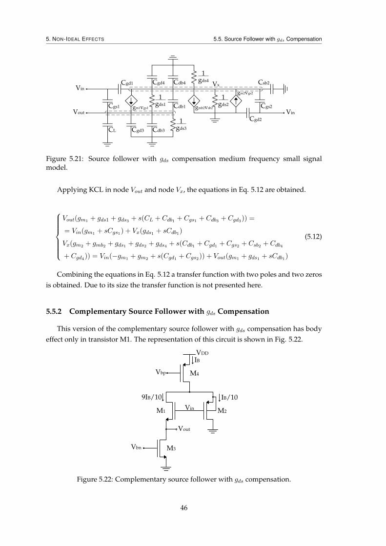
5. NON-IDEAL EFFECTS 5.5. Source Follower with gds Compensation
VinVx
Cgs1
Cgd1
Cgd3 Cdb3
Cdb1 gmb2vsb2
gm2vgs2
Csb2
Cgs2
Cgd2
Vout Vin
1 .
gds1
1 .
gds3
1 .
gds2gm1vgs1
Cgd4 Cdb4
1 .
gds4
CL
Figure 5.21: Source follower with gds compensation medium frequency small signalmodel.
Applying KCL in node Vout and node Vx, the equations in Eq. 5.12 are obtained.
Vout(gm1 + gds1 + gds3 + s(CL + Cdb1 + Cgs1 + Cdb3 + Cgd3)) =
= Vin(gm1 + sCgs1) + Vx(gds1 + sCdb1)
Vx(gm2 + gmb2 + gds1 + gds2 + gds4 + s(Cdb1 + Cgd1 + Cgs2 + Csb2 + Cdb4
+ Cgd4)) = Vin(−gm1 + gm2 + s(Cgd1 + Cgs2)) + Vout(gm1 + gds1 + sCdb1)
(5.12)
Combining the equations in Eq. 5.12 a transfer function with two poles and two zerosis obtained. Due to its size the transfer function is not presented here.
5.5.2 Complementary Source Follower with gds Compensation
This version of the complementary source follower with gds compensation has bodyeffect only in transistor M1. The representation of this circuit is shown in Fig. 5.22.
VDD
M4Vbp
IB
Vin
Vout
M2
IB/10
M1
M3Vbn
9IB/10
Figure 5.22: Complementary source follower with gds compensation.
46
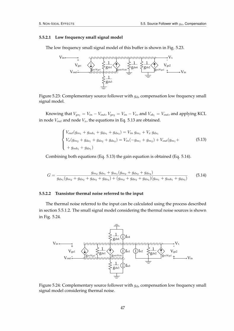
5. NON-IDEAL EFFECTS 5.5. Source Follower with gds Compensation
5.5.2.1 Low frequency small signal model
The low frequency small signal model of this buffer is shown in Fig. 5.23.
Vin Vx
gmb1vsb1 gm2vgs2
Vout Vin
1 .
gds1
1 .
gds3
1 .
gds2gm1vgs1
+
-
Vgs1
-
+
Vgs2 1 .
gds4
Figure 5.23: Complementary source follower with gds compensation low frequency smallsignal model.
Knowing that Vgs1 = Vin − Vout, Vgs2 = Vin − Vx, and Vsb1 = Vout, and applying KCLin node Vout and node Vx, the equations in Eq. 5.13 are obtained.
Vout(gm1 + gmb1 + gds1 + gds3) = Vin gm1 + Vx gds1
Vx(gm2 + gds1 + gds2 + gds4) = Vin(−gm1 + gm2) + Vout(gm1+
+ gmb1 + gds1)
(5.13)
Combining both equations (Eq. 5.13) the gain equation is obtained (Eq. 5.14).
G =gm2 gds1 + gm1(gm2 + gds2 + gds4)
gds1(gm2 + gds2 + gds3 + gds4) + (gm2 + gds2 + gds4)(gm1 + gmb1 + gds3)(5.14)
5.5.2.2 Transistor thermal noise referred to the input
The thermal noise referred to the input can be calculated using the process describedin section 5.5.1.2. The small signal model considering the thermal noise sources is shownin Fig. 5.24.
Vin Vx
gmb1vsb1 gm2vgs2
Vout Vin
1 .
gds1
1 .
gds3
1 .
gds2gm1vgs1
+
-
Vgs1
-
+
Vgs2
In3
In1
1 .
gds4In4
In2
Figure 5.24: Complementary source follower with gds compensation low frequency smallsignal model considering thermal noise.
47
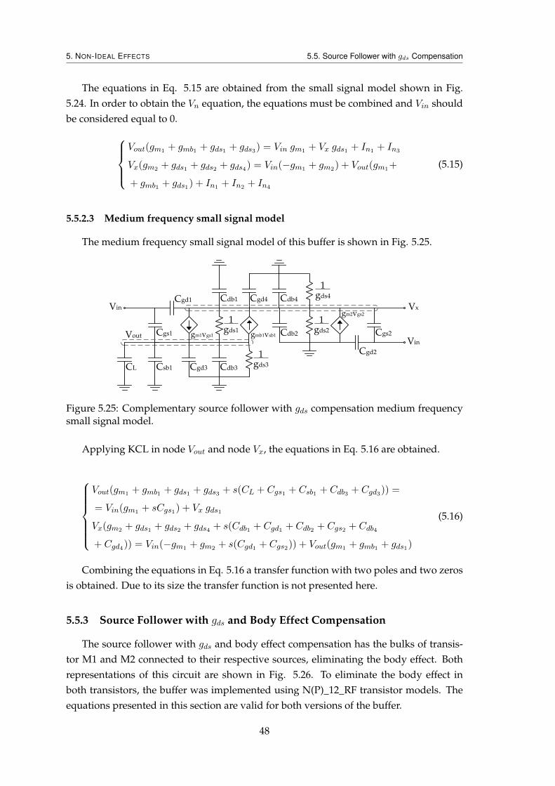
5. NON-IDEAL EFFECTS 5.5. Source Follower with gds Compensation
The equations in Eq. 5.15 are obtained from the small signal model shown in Fig.5.24. In order to obtain the Vn equation, the equations must be combined and Vin shouldbe considered equal to 0.
Vout(gm1 + gmb1 + gds1 + gds3) = Vin gm1 + Vx gds1 + In1 + In3
Vx(gm2 + gds1 + gds2 + gds4) = Vin(−gm1 + gm2) + Vout(gm1+
+ gmb1 + gds1) + In1 + In2 + In4
(5.15)
5.5.2.3 Medium frequency small signal model
The medium frequency small signal model of this buffer is shown in Fig. 5.25.
Vin
Cgs1
Cgd1
Cgd3 Cdb3
gm2vgs2
Cgs2
Cgd2
Vout
1 .
gds1
1 .
gds3
1 .
gds2gm1vgs1
Cgd4 Cdb4
1 .
gds4
gmb1vsb1 Cdb2
Vx
Vin
Csb1
Cdb1
CL
Figure 5.25: Complementary source follower with gds compensation medium frequencysmall signal model.
Applying KCL in node Vout and node Vx, the equations in Eq. 5.16 are obtained.
Vout(gm1 + gmb1 + gds1 + gds3 + s(CL + Cgs1 + Csb1 + Cdb3 + Cgd3)) =
= Vin(gm1 + sCgs1) + Vx gds1
Vx(gm2 + gds1 + gds2 + gds4 + s(Cdb1 + Cgd1 + Cdb2 + Cgs2 + Cdb4
+ Cgd4)) = Vin(−gm1 + gm2 + s(Cgd1 + Cgs2)) + Vout(gm1 + gmb1 + gds1)
(5.16)
Combining the equations in Eq. 5.16 a transfer function with two poles and two zerosis obtained. Due to its size the transfer function is not presented here.
5.5.3 Source Follower with gds and Body Effect Compensation
The source follower with gds and body effect compensation has the bulks of transis-tor M1 and M2 connected to their respective sources, eliminating the body effect. Bothrepresentations of this circuit are shown in Fig. 5.26. To eliminate the body effect inboth transistors, the buffer was implemented using N(P)_12_RF transistor models. Theequations presented in this section are valid for both versions of the buffer.
48
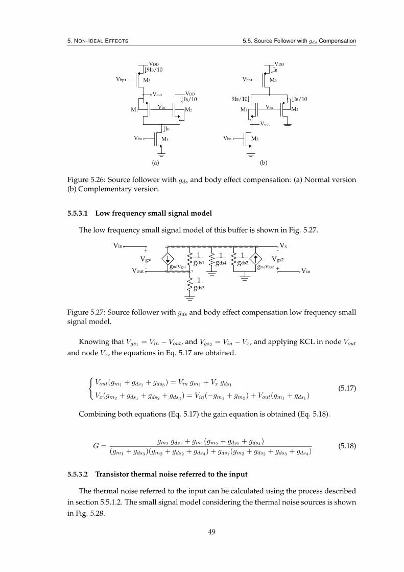
5. NON-IDEAL EFFECTS 5.5. Source Follower with gds Compensation
M3
M1 M2
M4
9IB/10
Vin
Vbp
Vout
VDD
VDD
Vbn
IB/10
IB
(a)
VDD
M4Vbp
IB
Vin
Vout
M2
IB/10
M1
M3Vbn
9IB/10
(b)
Figure 5.26: Source follower with gds and body effect compensation: (a) Normal version(b) Complementary version.
5.5.3.1 Low frequency small signal model
The low frequency small signal model of this buffer is shown in Fig. 5.27.
Vin Vx
gm2vgs2
Vout Vin
1 .
gds1
1 .
gds3
1 .
gds2 gm1vgs1
+
-
Vgs1
-
+
Vgs2 1 .
gds4
Figure 5.27: Source follower with gds and body effect compensation low frequency smallsignal model.
Knowing that Vgs1 = Vin − Vout, and Vgs2 = Vin − Vx, and applying KCL in node Voutand node Vx, the equations in Eq. 5.17 are obtained.
Vout(gm1 + gds1 + gds3) = Vin gm1 + Vx gds1
Vx(gm2 + gds1 + gds2 + gds4) = Vin(−gm1 + gm2) + Vout(gm1 + gds1)(5.17)
Combining both equations (Eq. 5.17) the gain equation is obtained (Eq. 5.18).
G =gm2 gds1 + gm1(gm2 + gds2 + gds4)
(gm1 + gds3)(gm2 + gds2 + gds4) + gds1(gm2 + gds2 + gds3 + gds4)(5.18)
5.5.3.2 Transistor thermal noise referred to the input
The thermal noise referred to the input can be calculated using the process describedin section 5.5.1.2. The small signal model considering the thermal noise sources is shownin Fig. 5.28.
49
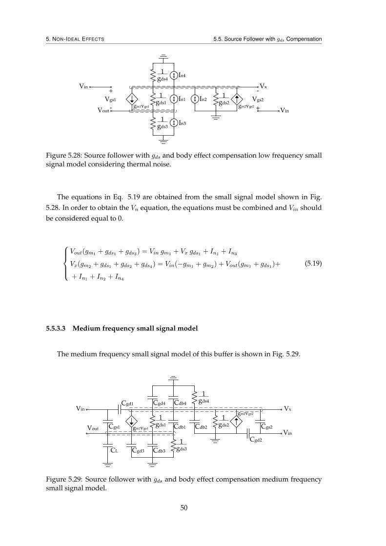
5. NON-IDEAL EFFECTS 5.5. Source Follower with gds Compensation
Vin Vx
Vout Vin
1 .
gds1
1 .
gds3
gm1vgs1
+
-
Vgs1
-
+
Vgs2
In3
In1
1 .
gds4In4
In2
gm2vgs2
1 .
gds2
Figure 5.28: Source follower with gds and body effect compensation low frequency smallsignal model considering thermal noise.
The equations in Eq. 5.19 are obtained from the small signal model shown in Fig.5.28. In order to obtain the Vn equation, the equations must be combined and Vin shouldbe considered equal to 0.
Vout(gm1 + gds1 + gds3) = Vin gm1 + Vx gds1 + In1 + In3
Vx(gm2 + gds1 + gds2 + gds4) = Vin(−gm1 + gm2) + Vout(gm1 + gds1)+
+ In1 + In2 + In4
(5.19)
5.5.3.3 Medium frequency small signal model
The medium frequency small signal model of this buffer is shown in Fig. 5.29.
Vin
Cgs1
Cgd1
Cgd3 Cdb3
gm2vgs2
Cgs2
Cgd2
Vout
1 .
gds1
1 .
gds3
1 .
gds2gm1vgs1
Cgd4 Cdb4
1 .
gds4
Cdb2
Vx
Vin
CL
Cdb1
Figure 5.29: Source follower with gds and body effect compensation medium frequencysmall signal model.
50
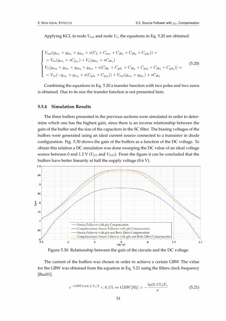
5. NON-IDEAL EFFECTS 5.5. Source Follower with gds Compensation
Applying KCL in node Vout and node Vx, the equations in Eq. 5.20 are obtained.
Vout(gm1 + gds1 + gds3 + s(CL + Cgs1 + Cdb1 + Cdb3 + Cgd3)) =
= Vin(gm1 + sCgs1) + Vx(gds1 + sCdb1)
Vx(gm2 + gds1 + gds2 + gds4 + s(Cdb1 + Cgd1 + Cdb2 + Cgs2 + Cdb4 + Cgd4)) =
= Vin(−gm1 + gm2 + s(Cgd1 + Cgs2)) + Vout(gm1 + gds1) + sCdb1
(5.20)
Combining the equations in Eq. 5.20 a transfer function with two poles and two zerosis obtained. Due to its size the transfer function is not presented here.
5.5.4 Simulation Results
The three buffers presented in the previous sections were simulated in order to deter-mine which one has the highest gain, since there is an inverse relationship between thegain of the buffer and the size of the capacitors in the SC filter. The biasing voltages of thebuffers were generated using an ideal current source connected to a transistor in diodeconfiguration. Fig. 5.30 shows the gain of the buffers as a function of the DC voltage. Toobtain this relation a DC simulation was done sweeping the DC value of an ideal voltagesource between 0 and 1.2 V (VSS and VDD). From the figure it can be concluded that thebuffers have better linearity at half the supply voltage (0.6 V).
Figure 5.30: Relationship between the gain of the circuits and the DC voltage.
The current of the buffers was chosen in order to achieve a certain GBW. The valuefor the GBW was obtained from the equation in Eq. 5.21 using the filters clock frequency[Raz01].
e−GBW [rad/s] Ts/2 < 0.1%⇔ GBW [Hz] > − ln(0.1%)Fs
π(5.21)
51
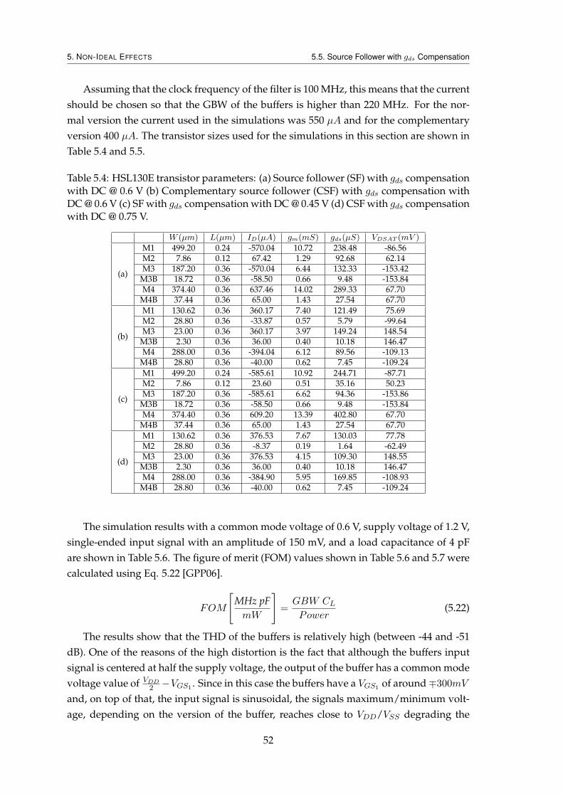
5. NON-IDEAL EFFECTS 5.5. Source Follower with gds Compensation
Assuming that the clock frequency of the filter is 100 MHz, this means that the currentshould be chosen so that the GBW of the buffers is higher than 220 MHz. For the nor-mal version the current used in the simulations was 550 µA and for the complementaryversion 400 µA. The transistor sizes used for the simulations in this section are shown inTable 5.4 and 5.5.
Table 5.4: HSL130E transistor parameters: (a) Source follower (SF) with gds compensationwith DC @ 0.6 V (b) Complementary source follower (CSF) with gds compensation withDC @ 0.6 V (c) SF with gds compensation with DC @ 0.45 V (d) CSF with gds compensationwith DC @ 0.75 V.
W (µm) L(µm) ID(µA) gm(mS) gds(µS) VDSAT (mV )
(a)
M1 499.20 0.24 -570.04 10.72 238.48 -86.56M2 7.86 0.12 67.42 1.29 92.68 62.14M3 187.20 0.36 -570.04 6.44 132.33 -153.42
M3B 18.72 0.36 -58.50 0.66 9.48 -153.84M4 374.40 0.36 637.46 14.02 289.33 67.70
M4B 37.44 0.36 65.00 1.43 27.54 67.70
(b)
M1 130.62 0.36 360.17 7.40 121.49 75.69M2 28.80 0.36 -33.87 0.57 5.79 -99.64M3 23.00 0.36 360.17 3.97 149.24 148.54
M3B 2.30 0.36 36.00 0.40 10.18 146.47M4 288.00 0.36 -394.04 6.12 89.56 -109.13
M4B 28.80 0.36 -40.00 0.62 7.45 -109.24
(c)
M1 499.20 0.24 -585.61 10.92 244.71 -87.71M2 7.86 0.12 23.60 0.51 35.16 50.23M3 187.20 0.36 -585.61 6.62 94.36 -153.86
M3B 18.72 0.36 -58.50 0.66 9.48 -153.84M4 374.40 0.36 609.20 13.39 402.80 67.70
M4B 37.44 0.36 65.00 1.43 27.54 67.70
(d)
M1 130.62 0.36 376.53 7.67 130.03 77.78M2 28.80 0.36 -8.37 0.19 1.64 -62.49M3 23.00 0.36 376.53 4.15 109.30 148.55
M3B 2.30 0.36 36.00 0.40 10.18 146.47M4 288.00 0.36 -384.90 5.95 169.85 -108.93
M4B 28.80 0.36 -40.00 0.62 7.45 -109.24
The simulation results with a common mode voltage of 0.6 V, supply voltage of 1.2 V,single-ended input signal with an amplitude of 150 mV, and a load capacitance of 4 pFare shown in Table 5.6. The figure of merit (FOM) values shown in Table 5.6 and 5.7 werecalculated using Eq. 5.22 [GPP06].
FOM
[MHz pFmW
]=GBW CL
Power(5.22)
The results show that the THD of the buffers is relatively high (between -44 and -51dB). One of the reasons of the high distortion is the fact that although the buffers inputsignal is centered at half the supply voltage, the output of the buffer has a common modevoltage value of VDD
2 −VGS1 . Since in this case the buffers have a VGS1 of around∓300mV
and, on top of that, the input signal is sinusoidal, the signals maximum/minimum volt-age, depending on the version of the buffer, reaches close to VDD/VSS degrading the
52
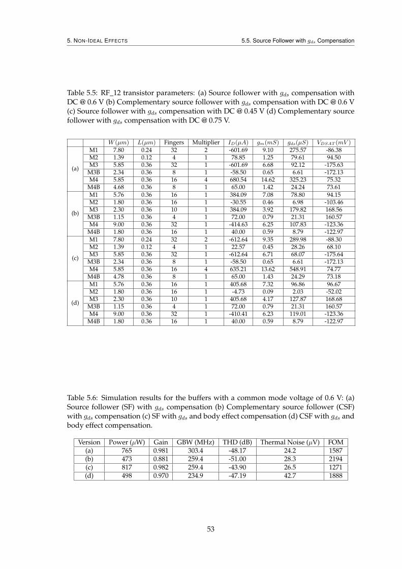
5. NON-IDEAL EFFECTS 5.5. Source Follower with gds Compensation
Table 5.5: RF_12 transistor parameters: (a) Source follower with gds compensation withDC @ 0.6 V (b) Complementary source follower with gds compensation with DC @ 0.6 V(c) Source follower with gds compensation with DC @ 0.45 V (d) Complementary sourcefollower with gds compensation with DC @ 0.75 V.
W (µm) L(µm) Fingers Multiplier ID(µA) gm(mS) gds(µS) VDSAT (mV )
(a)
M1 7.80 0.24 32 2 -601.69 9.10 275.57 -86.38M2 1.39 0.12 4 1 78.85 1.25 79.61 94.50M3 5.85 0.36 32 1 -601.69 6.68 92.12 -175.63
M3B 2.34 0.36 8 1 -58.50 0.65 6.61 -172.13M4 5.85 0.36 16 4 680.54 14.62 325.23 75.32
M4B 4.68 0.36 8 1 65.00 1.42 24.24 73.61
(b)
M1 5.76 0.36 16 1 384.09 7.08 78.80 94.15M2 1.80 0.36 16 1 -30.55 0.46 6.98 -103.46M3 2.30 0.36 10 1 384.09 3.92 179.82 168.56
M3B 1.15 0.36 4 1 72.00 0.79 21.31 160.57M4 9.00 0.36 32 1 -414.63 6.25 107.83 -123.36
M4B 1.80 0.36 16 1 40.00 0.59 8.79 -122.97
(c)
M1 7.80 0.24 32 2 -612.64 9.35 289.98 -88.30M2 1.39 0.12 4 1 22.57 0.45 28.26 68.10M3 5.85 0.36 32 1 -612.64 6.71 68.07 -175.64
M3B 2.34 0.36 8 1 -58.50 0.65 6.61 -172.13M4 5.85 0.36 16 4 635.21 13.62 548.91 74.77
M4B 4.78 0.36 8 1 65.00 1.43 24.29 73.18
(d)
M1 5.76 0.36 16 1 405.68 7.32 96.86 96.67M2 1.80 0.36 16 1 -4.73 0.09 2.03 -52.02M3 2.30 0.36 10 1 405.68 4.17 127.87 168.68
M3B 1.15 0.36 4 1 72.00 0.79 21.31 160.57M4 9.00 0.36 32 1 -410.41 6.23 119.01 -123.36
M4B 1.80 0.36 16 1 40.00 0.59 8.79 -122.97
Table 5.6: Simulation results for the buffers with a common mode voltage of 0.6 V: (a)Source follower (SF) with gds compensation (b) Complementary source follower (CSF)with gds compensation (c) SF with gds and body effect compensation (d) CSF with gds andbody effect compensation.
Version Power (µW) Gain GBW (MHz) THD (dB) Thermal Noise (µV) FOM(a) 765 0.981 303.4 -48.17 24.2 1587(b) 473 0.881 259.4 -51.00 28.3 2194(c) 817 0.982 259.4 -43.90 26.5 1271(d) 498 0.970 234.9 -47.19 42.7 1888
53
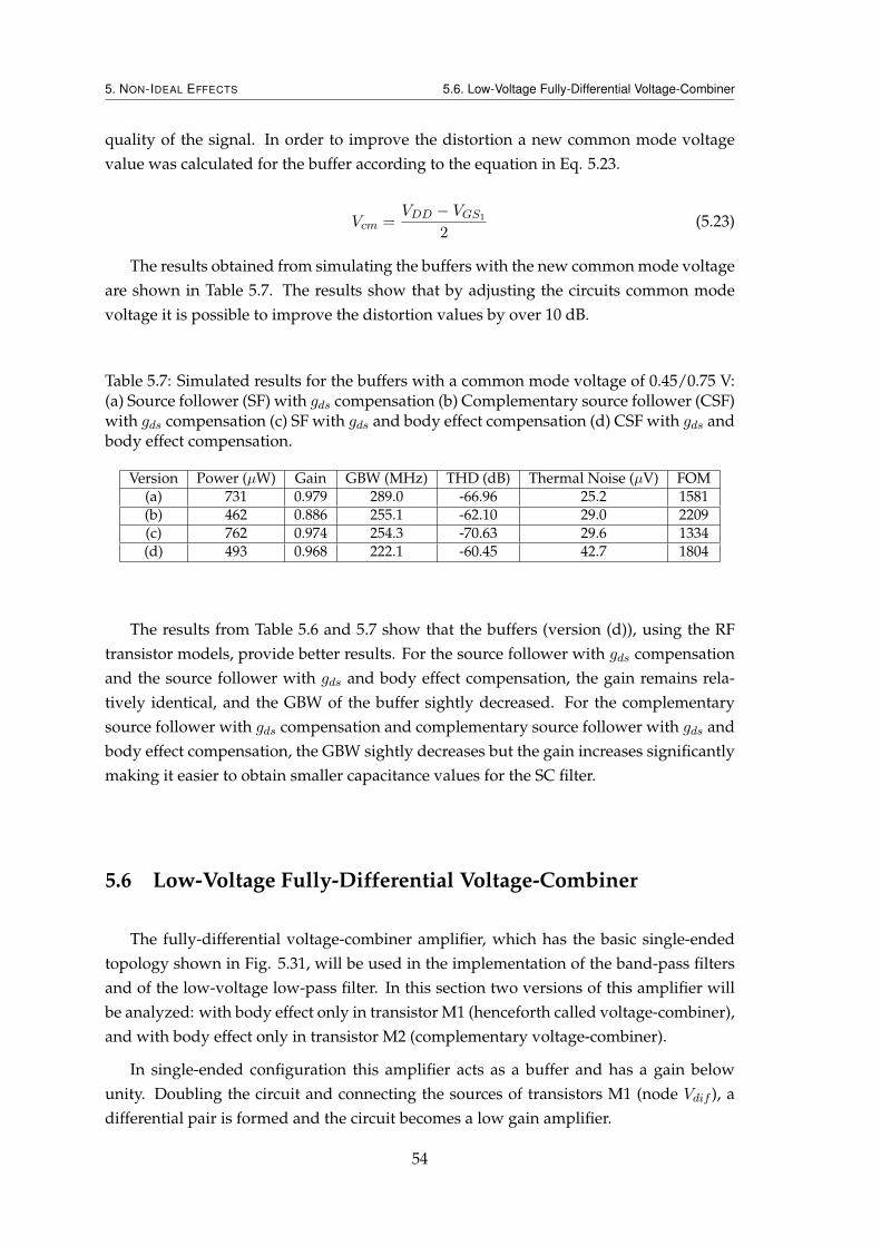
5. NON-IDEAL EFFECTS 5.6. Low-Voltage Fully-Differential Voltage-Combiner
quality of the signal. In order to improve the distortion a new common mode voltagevalue was calculated for the buffer according to the equation in Eq. 5.23.
Vcm =VDD − VGS1
2(5.23)
The results obtained from simulating the buffers with the new common mode voltageare shown in Table 5.7. The results show that by adjusting the circuits common modevoltage it is possible to improve the distortion values by over 10 dB.
Table 5.7: Simulated results for the buffers with a common mode voltage of 0.45/0.75 V:(a) Source follower (SF) with gds compensation (b) Complementary source follower (CSF)with gds compensation (c) SF with gds and body effect compensation (d) CSF with gds andbody effect compensation.
Version Power (µW) Gain GBW (MHz) THD (dB) Thermal Noise (µV) FOM(a) 731 0.979 289.0 -66.96 25.2 1581(b) 462 0.886 255.1 -62.10 29.0 2209(c) 762 0.974 254.3 -70.63 29.6 1334(d) 493 0.968 222.1 -60.45 42.7 1804
The results from Table 5.6 and 5.7 show that the buffers (version (d)), using the RFtransistor models, provide better results. For the source follower with gds compensationand the source follower with gds and body effect compensation, the gain remains rela-tively identical, and the GBW of the buffer sightly decreased. For the complementarysource follower with gds compensation and complementary source follower with gds andbody effect compensation, the GBW sightly decreases but the gain increases significantlymaking it easier to obtain smaller capacitance values for the SC filter.
5.6 Low-Voltage Fully-Differential Voltage-Combiner
The fully-differential voltage-combiner amplifier, which has the basic single-endedtopology shown in Fig. 5.31, will be used in the implementation of the band-pass filtersand of the low-voltage low-pass filter. In this section two versions of this amplifier willbe analyzed: with body effect only in transistor M1 (henceforth called voltage-combiner),and with body effect only in transistor M2 (complementary voltage-combiner).
In single-ended configuration this amplifier acts as a buffer and has a gain belowunity. Doubling the circuit and connecting the sources of transistors M1 (node Vdif ), adifferential pair is formed and the circuit becomes a low gain amplifier.
54
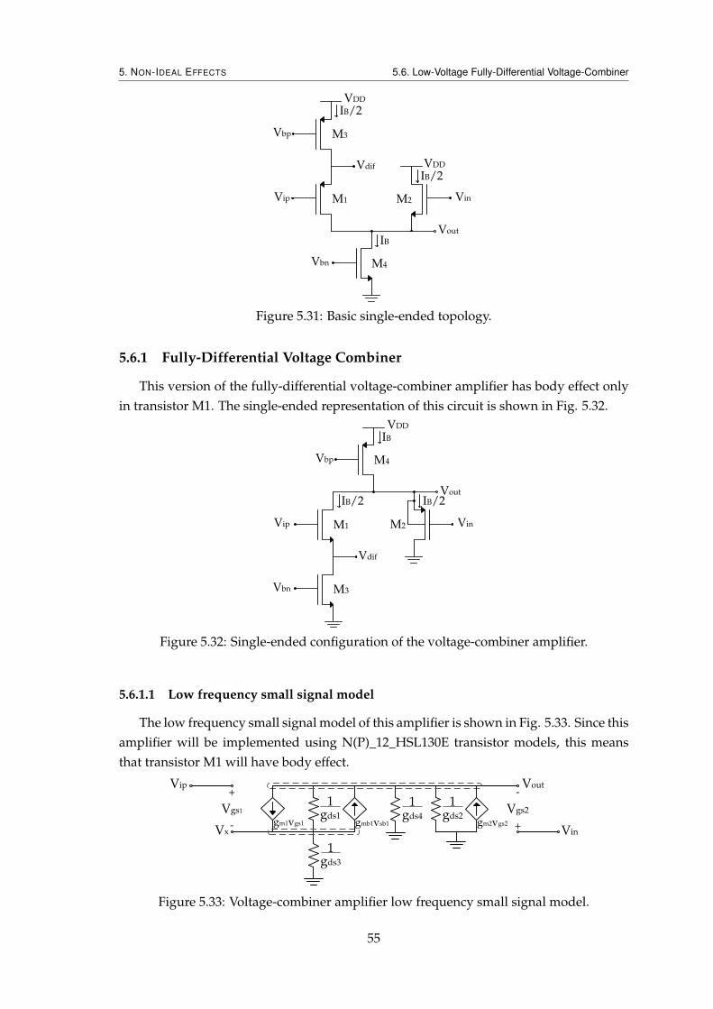
5. NON-IDEAL EFFECTS 5.6. Low-Voltage Fully-Differential Voltage-Combiner
Vbp
Vip
IB/2VDD
M3
M1
M4Vbn
IB
M2 Vin
VDD
IB/2
Vout
Vdif
Figure 5.31: Basic single-ended topology.
5.6.1 Fully-Differential Voltage Combiner
This version of the fully-differential voltage-combiner amplifier has body effect onlyin transistor M1. The single-ended representation of this circuit is shown in Fig. 5.32.
IB
VDD
Vbp
Vout
Vin
IB/2
M1Vip
IB/2
M3Vbn
M4
M2
Vdif
Figure 5.32: Single-ended configuration of the voltage-combiner amplifier.
5.6.1.1 Low frequency small signal model
The low frequency small signal model of this amplifier is shown in Fig. 5.33. Since thisamplifier will be implemented using N(P)_12_HSL130E transistor models, this meansthat transistor M1 will have body effect.
Vip Vout
gmb1vsb1 gm2vgs2
Vx Vin
1 .
gds1
1 .
gds3
1 .
gds2gm1vgs1
+
-
Vgs1
-
+
Vgs2 1 .
gds4
Figure 5.33: Voltage-combiner amplifier low frequency small signal model.
55
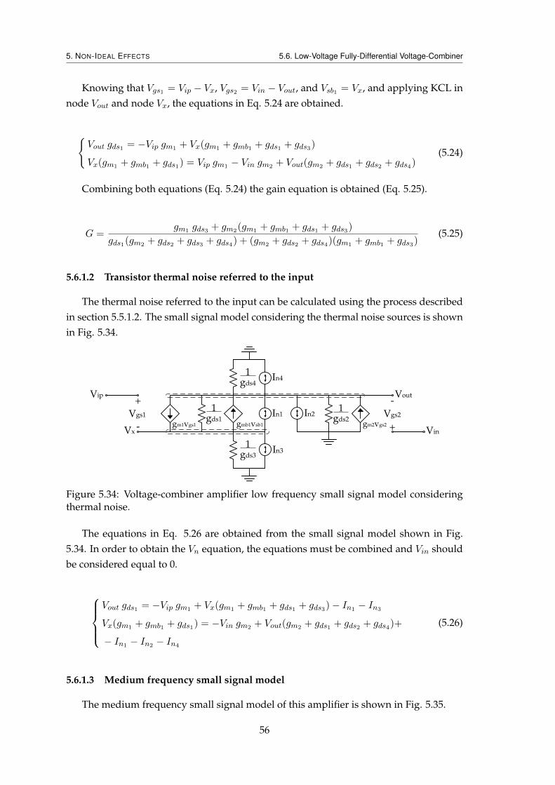
5. NON-IDEAL EFFECTS 5.6. Low-Voltage Fully-Differential Voltage-Combiner
Knowing that Vgs1 = Vip − Vx, Vgs2 = Vin − Vout, and Vsb1 = Vx, and applying KCL innode Vout and node Vx, the equations in Eq. 5.24 are obtained.
Vout gds1 = −Vip gm1 + Vx(gm1 + gmb1 + gds1 + gds3)
Vx(gm1 + gmb1 + gds1) = Vip gm1 − Vin gm2 + Vout(gm2 + gds1 + gds2 + gds4)(5.24)
Combining both equations (Eq. 5.24) the gain equation is obtained (Eq. 5.25).
G =gm1 gds3 + gm2(gm1 + gmb1 + gds1 + gds3)
gds1(gm2 + gds2 + gds3 + gds4) + (gm2 + gds2 + gds4)(gm1 + gmb1 + gds3)(5.25)
5.6.1.2 Transistor thermal noise referred to the input
The thermal noise referred to the input can be calculated using the process describedin section 5.5.1.2. The small signal model considering the thermal noise sources is shownin Fig. 5.34.
Vip Vout
gmb1vsb1 gm2vgs2
Vx Vin
1 .
gds1
1 .
gds3
1 .
gds2gm1vgs1
+
-
Vgs1
-
+
Vgs2
In3
In1
1 .
gds4In4
In2
Figure 5.34: Voltage-combiner amplifier low frequency small signal model consideringthermal noise.
The equations in Eq. 5.26 are obtained from the small signal model shown in Fig.5.34. In order to obtain the Vn equation, the equations must be combined and Vin shouldbe considered equal to 0.
Vout gds1 = −Vip gm1 + Vx(gm1 + gmb1 + gds1 + gds3)− In1 − In3
Vx(gm1 + gmb1 + gds1) = −Vin gm2 + Vout(gm2 + gds1 + gds2 + gds4)+
− In1 − In2 − In4
(5.26)
5.6.1.3 Medium frequency small signal model
The medium frequency small signal model of this amplifier is shown in Fig. 5.35.
56
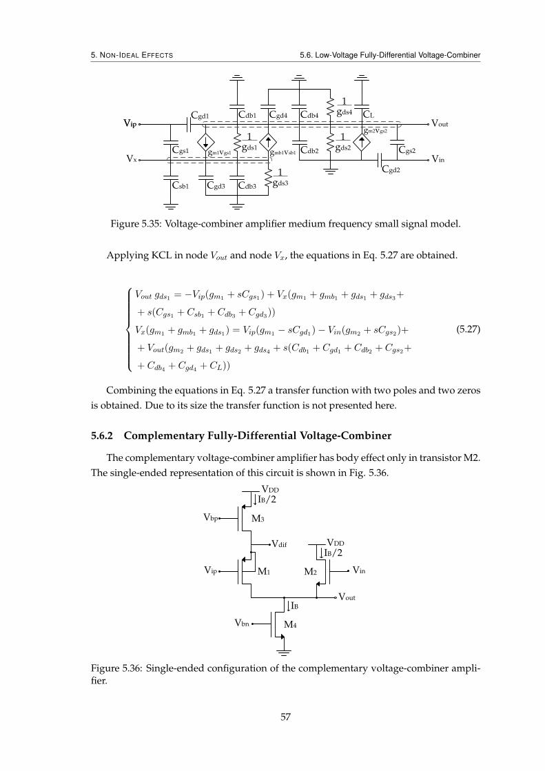
5. NON-IDEAL EFFECTS 5.6. Low-Voltage Fully-Differential Voltage-Combiner
Vip
Cgs1
Cgd1
Cgd3 Cdb3
gm2vgs2
Cgs2
Cgd2
1 .
gds1
1 .
gds3
1 .
gds2gm1vgs1
Cgd4 Cdb4
1 .
gds4
gmb1vsb1 Cdb2
Vout
Vin
Csb1
Cdb1 CL
Vip
Vx
Figure 5.35: Voltage-combiner amplifier medium frequency small signal model.
Applying KCL in node Vout and node Vx, the equations in Eq. 5.27 are obtained.
Vout gds1 = −Vip(gm1 + sCgs1) + Vx(gm1 + gmb1 + gds1 + gds3+
+ s(Cgs1 + Csb1 + Cdb3 + Cgd3))
Vx(gm1 + gmb1 + gds1) = Vip(gm1 − sCgd1)− Vin(gm2 + sCgs2)+
+ Vout(gm2 + gds1 + gds2 + gds4 + s(Cdb1 + Cgd1 + Cdb2 + Cgs2+
+ Cdb4 + Cgd4 + CL))
(5.27)
Combining the equations in Eq. 5.27 a transfer function with two poles and two zerosis obtained. Due to its size the transfer function is not presented here.
5.6.2 Complementary Fully-Differential Voltage-Combiner
The complementary voltage-combiner amplifier has body effect only in transistor M2.The single-ended representation of this circuit is shown in Fig. 5.36.
Vbp
Vip
IB/2VDD
M3
M4Vbn
IB
M2 Vin
VDD
IB/2
Vout
M1
Vdif
Figure 5.36: Single-ended configuration of the complementary voltage-combiner ampli-fier.
57
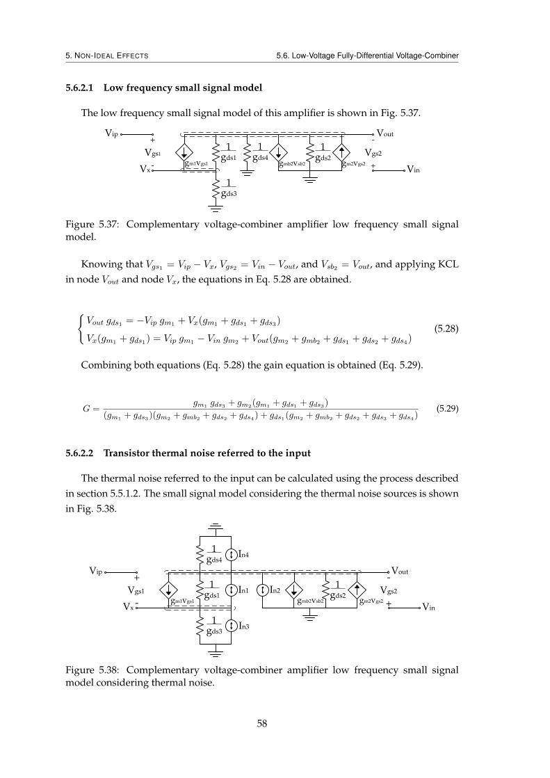
5. NON-IDEAL EFFECTS 5.6. Low-Voltage Fully-Differential Voltage-Combiner
5.6.2.1 Low frequency small signal model
The low frequency small signal model of this amplifier is shown in Fig. 5.37.
Vip Vout
gmb2vsb2 gm2vgs2
Vx Vin
1 .
gds1
1 .
gds3
1 .
gds2gm1vgs1
1 .
gds4
+
-
Vgs1
-
+
Vgs2
Figure 5.37: Complementary voltage-combiner amplifier low frequency small signalmodel.
Knowing that Vgs1 = Vip − Vx, Vgs2 = Vin − Vout, and Vsb2 = Vout, and applying KCLin node Vout and node Vx, the equations in Eq. 5.28 are obtained.
Vout gds1 = −Vip gm1 + Vx(gm1 + gds1 + gds3)
Vx(gm1 + gds1) = Vip gm1 − Vin gm2 + Vout(gm2 + gmb2 + gds1 + gds2 + gds4)(5.28)
Combining both equations (Eq. 5.28) the gain equation is obtained (Eq. 5.29).
G =gm1
gds3 + gm2(gm1
+ gds1 + gds3)
(gm1+ gds3)(gm2
+ gmb2 + gds2 + gds4) + gds1(gm2+ gmb2 + gds2 + gds3 + gds4)
(5.29)
5.6.2.2 Transistor thermal noise referred to the input
The thermal noise referred to the input can be calculated using the process describedin section 5.5.1.2. The small signal model considering the thermal noise sources is shownin Fig. 5.38.
Vip Vout
gmb2vsb2 gm2vgs2
Vx Vin
1 .
gds1
1 .
gds3
1 .
gds2gm1vgs1
+
-
Vgs1
-
+
Vgs2
In3
In1
1 .
gds4In4
In2
Figure 5.38: Complementary voltage-combiner amplifier low frequency small signalmodel considering thermal noise.
58
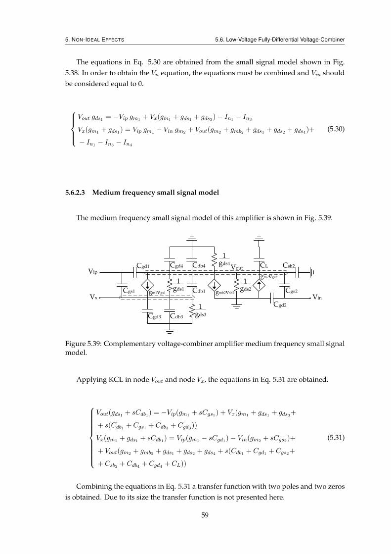
5. NON-IDEAL EFFECTS 5.6. Low-Voltage Fully-Differential Voltage-Combiner
The equations in Eq. 5.30 are obtained from the small signal model shown in Fig.5.38. In order to obtain the Vn equation, the equations must be combined and Vin shouldbe considered equal to 0.
Vout gds1 = −Vip gm1 + Vx(gm1 + gds1 + gds3)− In1 − In3
Vx(gm1 + gds1) = Vip gm1 − Vin gm2 + Vout(gm2 + gmb2 + gds1 + gds2 + gds4)+
− In1 − In3 − In4
(5.30)
5.6.2.3 Medium frequency small signal model
The medium frequency small signal model of this amplifier is shown in Fig. 5.39.
VipVout
Cgs1
Cgd1
Cgd3 Cdb3
Cdb1 gmb2vsb2
gm2vgs2
Csb2
Cgs2
Cgd2
Vx Vin
1 .
gds1
1 .
gds3
1 .
gds2gm1vgs1
Cgd4 Cdb4
1 .
gds4 CL
Figure 5.39: Complementary voltage-combiner amplifier medium frequency small signalmodel.
Applying KCL in node Vout and node Vx, the equations in Eq. 5.31 are obtained.
Vout(gds1 + sCdb1) = −Vip(gm1 + sCgs1) + Vx(gm1 + gds1 + gds3+
+ s(Cdb1 + Cgs1 + Cdb3 + Cgd3))
Vx(gm1 + gds1 + sCdb1) = Vip(gm1 − sCgd1)− Vin(gm2 + sCgs2)+
+ Vout(gm2 + gmb2 + gds1 + gds2 + gds4 + s(Cdb1 + Cgd1 + Cgs2+
+ Csb2 + Cdb4 + Cgd4 + CL))
(5.31)
Combining the equations in Eq. 5.31 a transfer function with two poles and two zerosis obtained. Due to its size the transfer function is not presented here.
59
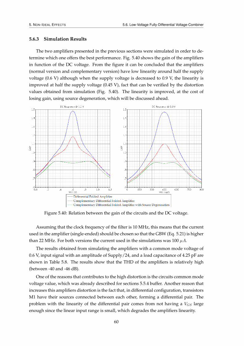
5. NON-IDEAL EFFECTS 5.6. Low-Voltage Fully-Differential Voltage-Combiner
5.6.3 Simulation Results
The two amplifiers presented in the previous sections were simulated in order to de-termine which one offers the best performance. Fig. 5.40 shows the gain of the amplifiersin function of the DC voltage. From the figure it can be concluded that the amplifiers(normal version and complementary version) have low linearity around half the supplyvoltage (0.6 V) although when the supply voltage is decreased to 0.9 V, the linearity isimproved at half the supply voltage (0.45 V), fact that can be verified by the distortionvalues obtained from simulation (Fig. 5.40). The linearity is improved, at the cost oflosing gain, using source degeneration, which will be discussed ahead.
Figure 5.40: Relation between the gain of the circuits and the DC voltage.
Assuming that the clock frequency of the filter is 10 MHz, this means that the currentused in the amplifier (single-ended) should be chosen so that the GBW (Eq. 5.21) is higherthan 22 MHz. For both versions the current used in the simulations was 100 µA.
The results obtained from simulating the amplifiers with a common mode voltage of0.6 V, input signal with an amplitude of Supply/24, and a load capacitance of 4.25 pF areshown in Table 5.8. The results show that the THD of the amplifiers is relatively high(between -40 and -46 dB).
One of the reasons that contributes to the high distortion is the circuits common modevoltage value, which was already described for sections 5.5.4 buffer. Another reason thatincreases this amplifiers distortion is the fact that, in differential configuration, transistorsM1 have their sources connected between each other, forming a differential pair. Theproblem with the linearity of the differential pair comes from not having a VGS largeenough since the linear input range is small, which degrades the amplifiers linearity.
60
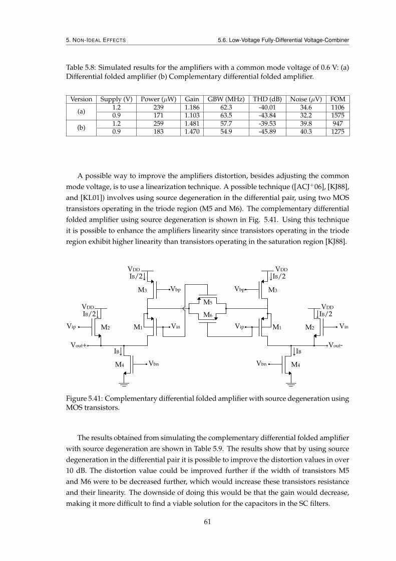
5. NON-IDEAL EFFECTS 5.6. Low-Voltage Fully-Differential Voltage-Combiner
Table 5.8: Simulated results for the amplifiers with a common mode voltage of 0.6 V: (a)Differential folded amplifier (b) Complementary differential folded amplifier.
Version Supply (V) Power (µW) Gain GBW (MHz) THD (dB) Noise (µV) FOM
(a) 1.2 239 1.186 62.3 -40.01 34.6 11060.9 171 1.103 63.5 -43.84 32.2 1575
(b) 1.2 259 1.481 57.7 -39.53 39.8 9470.9 183 1.470 54.9 -45.89 40.3 1275
A possible way to improve the amplifiers distortion, besides adjusting the commonmode voltage, is to use a linearization technique. A possible technique ([ACJ+06], [KJ88],and [KL01]) involves using source degeneration in the differential pair, using two MOStransistors operating in the triode region (M5 and M6). The complementary differentialfolded amplifier using source degeneration is shown in Fig. 5.41. Using this techniqueit is possible to enhance the amplifiers linearity since transistors operating in the trioderegion exhibit higher linearity than transistors operating in the saturation region [KJ88].
M5
M6
Vbp
Vip
IB/2VDD
M3
M4Vbn
IB
M2 Vin
VDD
IB/2
Vout-
M1
Vbp
Vin
IB/2VDD
M3
M4 Vbn
IB
M2Vip
VDD
IB/2
Vout+
M1
Figure 5.41: Complementary differential folded amplifier with source degeneration usingMOS transistors.
The results obtained from simulating the complementary differential folded amplifierwith source degeneration are shown in Table 5.9. The results show that by using sourcedegeneration in the differential pair it is possible to improve the distortion values in over10 dB. The distortion value could be improved further if the width of transistors M5and M6 were to be decreased further, which would increase these transistors resistanceand their linearity. The downside of doing this would be that the gain would decrease,making it more difficult to find a viable solution for the capacitors in the SC filters.
61
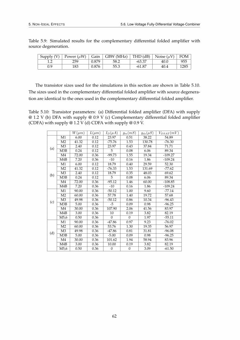
5. NON-IDEAL EFFECTS 5.6. Low-Voltage Fully-Differential Voltage-Combiner
Table 5.9: Simulated results for the complementary differential folded amplifier withsource degeneration.
Supply (V) Power (µW) Gain GBW (MHz) THD (dB) Noise (µV) FOM1.2 259 0.879 58.2 -63.37 40.0 9550.9 183 0.876 55.3 -61.87 40.4 1285
The transistor sizes used for the simulations in this section are shown in Table 5.10.The sizes used in the complementary differential folded amplifier with source degenera-tion are identical to the ones used in the complementary differential folded amplifier.
Table 5.10: Transistor parameters: (a) Differential folded amplifier (DFA) with supply@ 1.2 V (b) DFA with supply @ 0.9 V (c) Complementary differential folded amplifier(CDFA) with supply @ 1.2 V (d) CDFA with supply @ 0.9 V.
W (µm) L(µm) ID(µA) gm(mS) gds(µS) VDSAT (mV )
(a)
M1 6.00 0.12 23.97 0.51 38.22 54.89M2 41.32 0.12 -75.76 1.53 130.78 -76.30M3 2.40 0.12 23.97 0.43 37.84 71.71
M3B 0.24 0.12 5 0.08 6.06 89.34M4 72.00 0.36 -99.73 1.55 19.34 -109.27
M4B 7.20 0.36 -10 0.16 1.86 -109.24
(b)
M1 6.00 0.12 18.79 0.40 29.59 52.30M2 41.32 0.12 -76.33 1.53 131.69 -77.62M3 2.40 0.12 18.79 0.35 48.03 69.62
M3B 0.24 0.12 5 0.08 6.06 89.34M4 72.00 0.36 -95.12 1.46 60.00 -108.85
M4B 7.20 0.36 -10 0.16 1.86 -109.24
(c)
M1 90.00 0.36 -50.12 1.00 9.60 -77.14M2 60.00 0.36 57.78 1.40 19.72 57.68M3 49.98 0.36 -50.12 0.86 10.34 -96.43
M3B 5.00 0.36 -5 0.09 0.98 -96.25M4 30.00 0.36 107.90 2.06 41.56 83.97
M4B 3.00 0.36 10 0.19 3.82 82.19M5,6 0.50 0.36 0 0 1.97 -55.11
(d)
M1 90.00 0.36 -47.86 0.97 9.23 -76.02M2 60.00 0.36 53.76 1.30 19.35 56.97M3 49.98 0.36 -47.86 0.81 31.81 -96.08
M3B 5.00 0.36 -5.00 0.09 0.98 -96.25M4 30.00 0.36 101.62 1.94 58.94 83.96
M4B 3.00 0.36 10.00 0.19 3.82 82.19M5,6 0.50 0.36 0 0 3.09 -61.50
62
6Switched Capacitor Filter
Implementation
6.1 Introduction
In the previous chapter the non-ideal effects of using real components were presentedand discussed. In this chapter the filter circuits will be simulated taking into account thenon-ideal effects. Due to these effects the band-pass filter will be altered, adding a newcapacitor to the circuit. This is done in order to take into account the input capacitance ofthe low gain amplifier and facilitate the compensation of this capacitance.
6.2 Second-Order Low-Pass SC Filter
The simulation results of the second-order low-pass SC filter using real componentswill be presented in this section. The results of the simulations will be presented when allcomponents are ideal, when the switches are real and the remaining components ideal,when the buffers/amplifiers are real and the remaining components ideal, and when allcomponents are real in order to determine the influence of each real component in theoverall performance of the filter.
When replacing the ideal buffer with a real buffer the value of capacitance C2 mustbe recalculated in order to compensate the input capacitance of the real buffer. An ap-proximate value for the input capacitance can be obtained from the DC simulation ofthe circuit. When using real switches instead of ideal, the filters capacitance values mustalso be recalculated in order to compensate the switches parasitic capacitances Cd andCs. An approximate value for these capacitances can also be obtained from the DC simu-lation. The single-ended version of the low-pass filter considering the switches parasiticcapacitances and the buffers input capacitance is shown in Fig. 6.1.
63
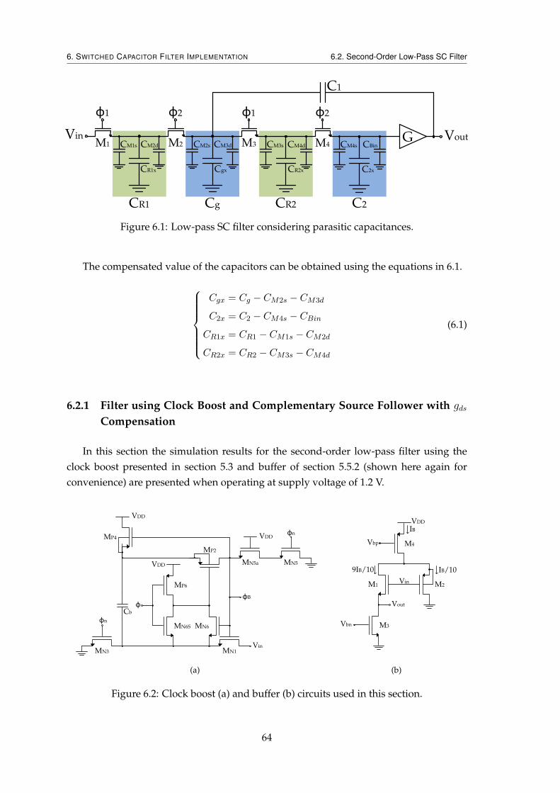
6. SWITCHED CAPACITOR FILTER IMPLEMENTATION 6.2. Second-Order Low-Pass SC Filter
C2CR2Cg
Vin VoutG
φ1
CR1x
C1
CM1sM1
φ2
M2CM2d
CR1
Cgx
CM2s
φ1
M3CM3d CM3s
CR2x
φ2
M4CM4d CM4s
C2x
CBin
Figure 6.1: Low-pass SC filter considering parasitic capacitances.
The compensated value of the capacitors can be obtained using the equations in 6.1.
Cgx = Cg − CM2s − CM3d
C2x = C2 − CM4s − CBin
CR1x = CR1 − CM1s − CM2d
CR2x = CR2 − CM3s − CM4d
(6.1)
6.2.1 Filter using Clock Boost and Complementary Source Follower with gds
Compensation
In this section the simulation results for the second-order low-pass filter using theclock boost presented in section 5.3 and buffer of section 5.5.2 (shown here again forconvenience) are presented when operating at supply voltage of 1.2 V.
φ
φn
Vin
VDD
VDD
VDD
Cb
MN5a MN5
MN1
MN6S MN6
MP6
MP2
MP4
φB
φn
MN3
(a)
VDD
M4Vbp
IB
Vin
Vout
M2
IB/10
M1
M3Vbn
9IB/10
(b)
Figure 6.2: Clock boost (a) and buffer (b) circuits used in this section.
64
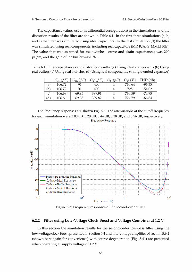
6. SWITCHED CAPACITOR FILTER IMPLEMENTATION 6.2. Second-Order Low-Pass SC Filter
The capacitance values used (in differential configuration) in the simulations and thedistortion results of the filter are shown in Table 6.1. In the first three simulations (a, b,and c) the filter was simulated using ideal capacitors. In the last simulation (d) the filterwas simulated using real components, including real capacitors (MIMCAPS_MML130E).The value that was assumed for the switches source and drain capacitances was 290pF/m, and the gain of the buffer was 0.97.
Table 6.1: Filter capacitances and distortion results: (a) Using ideal components (b) Usingreal buffers (c) Using real switches (d) Using real components. (? single-ended capacitor)
CR1(fF ) CR2(fF ) Cg?(fF ) C1
?(pF ) C2(fF ) THD (dB)(a) 106.72 70 400 4 760.64 -96.35(b) 106.72 70 400 4 725 -54.02(c) 106.68 69.95 399.91 4 760.59 -74.95(d) 106.66 69.98 399.82 4 724.79 -66.84
The frequency responses are shown Fig. 6.3. The attenuations at the cutoff frequencyfor each simulation were 3.00 dB, 3.28 dB, 3.44 dB, 3.38 dB, and 3.56 dB, respectively.
Figure 6.3: Frequency responses of the second-order filter.
6.2.2 Filter using Low-Voltage Clock Boost and Voltage Combiner at 1.2 V
In this section the simulation results for the second-order low-pass filter using thelow-voltage clock boost presented in section 5.4 and low-voltage amplifier of section 5.6.2(shown here again for convenience) with source degeneration (Fig. 5.41) are presentedwhen operating at supply voltage of 1.2 V.
65
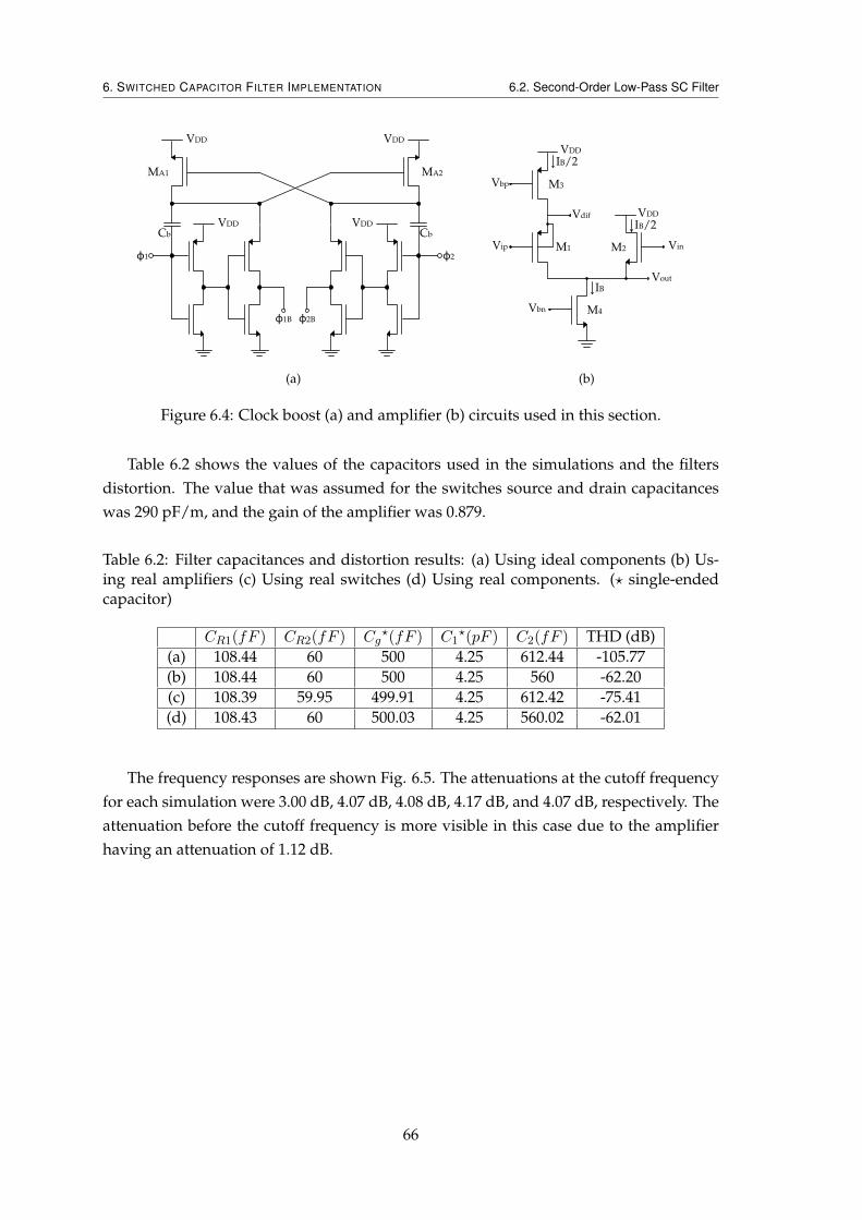
6. SWITCHED CAPACITOR FILTER IMPLEMENTATION 6.2. Second-Order Low-Pass SC Filter
φ1
φ1B
Cb
VDD
MA1
VDD
φ2
φ2B
Cb
VDD
MA2
VDD
(a)
Vbp
Vip
IB/2VDD
M3
M4Vbn
IB
M2 Vin
VDD
IB/2
Vout
M1
Vdif
(b)
Figure 6.4: Clock boost (a) and amplifier (b) circuits used in this section.
Table 6.2 shows the values of the capacitors used in the simulations and the filtersdistortion. The value that was assumed for the switches source and drain capacitanceswas 290 pF/m, and the gain of the amplifier was 0.879.
Table 6.2: Filter capacitances and distortion results: (a) Using ideal components (b) Us-ing real amplifiers (c) Using real switches (d) Using real components. (? single-endedcapacitor)
CR1(fF ) CR2(fF ) Cg?(fF ) C1
?(pF ) C2(fF ) THD (dB)(a) 108.44 60 500 4.25 612.44 -105.77(b) 108.44 60 500 4.25 560 -62.20(c) 108.39 59.95 499.91 4.25 612.42 -75.41(d) 108.43 60 500.03 4.25 560.02 -62.01
The frequency responses are shown Fig. 6.5. The attenuations at the cutoff frequencyfor each simulation were 3.00 dB, 4.07 dB, 4.08 dB, 4.17 dB, and 4.07 dB, respectively. Theattenuation before the cutoff frequency is more visible in this case due to the amplifierhaving an attenuation of 1.12 dB.
66
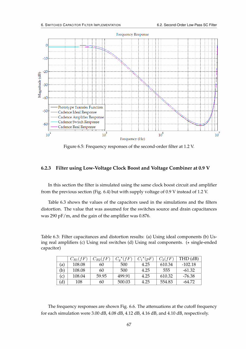
6. SWITCHED CAPACITOR FILTER IMPLEMENTATION 6.2. Second-Order Low-Pass SC Filter
Figure 6.5: Frequency responses of the second-order filter at 1.2 V.
6.2.3 Filter using Low-Voltage Clock Boost and Voltage Combiner at 0.9 V
In this section the filter is simulated using the same clock boost circuit and amplifierfrom the previous section (Fig. 6.4) but with supply voltage of 0.9 V instead of 1.2 V.
Table 6.3 shows the values of the capacitors used in the simulations and the filtersdistortion. The value that was assumed for the switches source and drain capacitanceswas 290 pF/m, and the gain of the amplifier was 0.876.
Table 6.3: Filter capacitances and distortion results: (a) Using ideal components (b) Us-ing real amplifiers (c) Using real switches (d) Using real components. (? single-endedcapacitor)
CR1(fF ) CR2(fF ) Cg?(fF ) C1
?(pF ) C2(fF ) THD (dB)(a) 108.08 60 500 4.25 610.34 -102.18(b) 108.08 60 500 4.25 555 -61.32(c) 108.04 59.95 499.91 4.25 610.32 -76.38(d) 108 60 500.03 4.25 554.83 -64.72
The frequency responses are shown Fig. 6.6. The attenuations at the cutoff frequencyfor each simulation were 3.00 dB, 4.08 dB, 4.12 dB, 4.16 dB, and 4.10 dB, respectively.
67
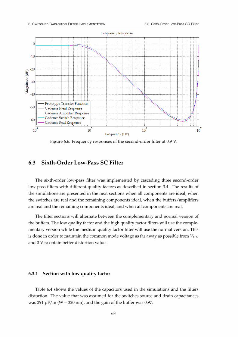
6. SWITCHED CAPACITOR FILTER IMPLEMENTATION 6.3. Sixth-Order Low-Pass SC Filter
Figure 6.6: Frequency responses of the second-order filter at 0.9 V.
6.3 Sixth-Order Low-Pass SC Filter
The sixth-order low-pass filter was implemented by cascading three second-orderlow-pass filters with different quality factors as described in section 3.4. The results ofthe simulations are presented in the next sections when all components are ideal, whenthe switches are real and the remaining components ideal, when the buffers/amplifiersare real and the remaining components ideal, and when all components are real.
The filter sections will alternate between the complementary and normal version ofthe buffers. The low quality factor and the high quality factor filters will use the comple-mentary version while the medium quality factor filter will use the normal version. Thisis done in order to maintain the common mode voltage as far away as possible from VDD
and 0 V to obtain better distortion values.
6.3.1 Section with low quality factor
Table 6.4 shows the values of the capacitors used in the simulations and the filtersdistortion. The value that was assumed for the switches source and drain capacitanceswas 291 pF/m (W = 320 nm), and the gain of the buffer was 0.97.
68
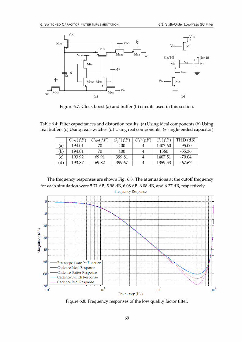
6. SWITCHED CAPACITOR FILTER IMPLEMENTATION 6.3. Sixth-Order Low-Pass SC Filter
φ
φn
Vin
VDD
VDD
VDD
Cb
MN5a MN5
MN1
MN6S MN6
MP6
MP2
MP4
φB
φn
MN3
(a)
VDD
M4Vbp
IB
Vin
Vout
M2
IB/10
M1
M3Vbn
9IB/10
(b)
Figure 6.7: Clock boost (a) and buffer (b) circuits used in this section.
Table 6.4: Filter capacitances and distortion results: (a) Using ideal components (b) Usingreal buffers (c) Using real switches (d) Using real components. (? single-ended capacitor)
CR1(fF ) CR2(fF ) Cg?(fF ) C1
?(pF ) C2(fF ) THD (dB)(a) 194.01 70 400 4 1407.60 -95.00(b) 194.01 70 400 4 1360 -55.36(c) 193.92 69.91 399.81 4 1407.51 -70.04(d) 193.87 69.82 399.67 4 1359.53 -67.67
The frequency responses are shown Fig. 6.8. The attenuations at the cutoff frequencyfor each simulation were 5.71 dB, 5.98 dB, 6.08 dB, 6.08 dB, and 6.27 dB, respectively.
Figure 6.8: Frequency responses of the low quality factor filter.
69
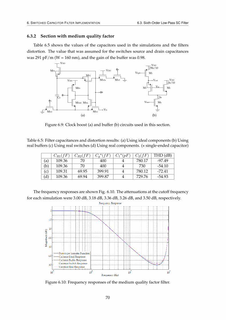
6. SWITCHED CAPACITOR FILTER IMPLEMENTATION 6.3. Sixth-Order Low-Pass SC Filter
6.3.2 Section with medium quality factor
Table 6.5 shows the values of the capacitors used in the simulations and the filtersdistortion. The value that was assumed for the switches source and drain capacitanceswas 291 pF/m (W = 160 nm), and the gain of the buffer was 0.98.
φ
φn
Vin
VDD
VDD
VDD
Cb
MN5a MN5
MN1
MN6S MN6
MP6
MP2
MP4
φB
φn
MN3
(a)
M3
M1 M2
M4
9IB/10
Vin
Vbp
Vout
VDD
VDD
Vbn
IB/10
IB
(b)
Figure 6.9: Clock boost (a) and buffer (b) circuits used in this section.
Table 6.5: Filter capacitances and distortion results: (a) Using ideal components (b) Usingreal buffers (c) Using real switches (d) Using real components. (? single-ended capacitor)
CR1(fF ) CR2(fF ) Cg?(fF ) C1
?(pF ) C2(fF ) THD (dB)(a) 109.36 70 400 4 780.17 -97.49(b) 109.36 70 400 4 730 -54.10(c) 109.31 69.95 399.91 4 780.12 -72.41(d) 109.36 69.94 399.87 4 729.76 -54.93
The frequency responses are shown Fig. 6.10. The attenuations at the cutoff frequencyfor each simulation were 3.00 dB, 3.18 dB, 3.36 dB, 3.26 dB, and 3.50 dB, respectively.
Figure 6.10: Frequency responses of the medium quality factor filter.
70
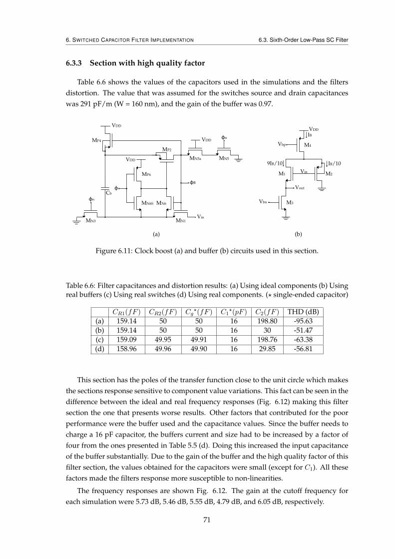
6. SWITCHED CAPACITOR FILTER IMPLEMENTATION 6.3. Sixth-Order Low-Pass SC Filter
6.3.3 Section with high quality factor
Table 6.6 shows the values of the capacitors used in the simulations and the filtersdistortion. The value that was assumed for the switches source and drain capacitanceswas 291 pF/m (W = 160 nm), and the gain of the buffer was 0.97.
φ
φn
Vin
VDD
VDD
VDD
Cb
MN5a MN5
MN1
MN6S MN6
MP6
MP2
MP4
φB
φn
MN3
(a)
VDD
M4Vbp
IB
Vin
Vout
M2
IB/10
M1
M3Vbn
9IB/10
(b)
Figure 6.11: Clock boost (a) and buffer (b) circuits used in this section.
Table 6.6: Filter capacitances and distortion results: (a) Using ideal components (b) Usingreal buffers (c) Using real switches (d) Using real components. (? single-ended capacitor)
CR1(fF ) CR2(fF ) Cg?(fF ) C1
?(pF ) C2(fF ) THD (dB)(a) 159.14 50 50 16 198.80 -95.63(b) 159.14 50 50 16 30 -51.47(c) 159.09 49.95 49.91 16 198.76 -63.38(d) 158.96 49.96 49.90 16 29.85 -56.81
This section has the poles of the transfer function close to the unit circle which makesthe sections response sensitive to component value variations. This fact can be seen in thedifference between the ideal and real frequency responses (Fig. 6.12) making this filtersection the one that presents worse results. Other factors that contributed for the poorperformance were the buffer used and the capacitance values. Since the buffer needs tocharge a 16 pF capacitor, the buffers current and size had to be increased by a factor offour from the ones presented in Table 5.5 (d). Doing this increased the input capacitanceof the buffer substantially. Due to the gain of the buffer and the high quality factor of thisfilter section, the values obtained for the capacitors were small (except for C1). All thesefactors made the filters response more susceptible to non-linearities.
The frequency responses are shown Fig. 6.12. The gain at the cutoff frequency foreach simulation were 5.73 dB, 5.46 dB, 5.55 dB, 4.79 dB, and 6.05 dB, respectively.
71
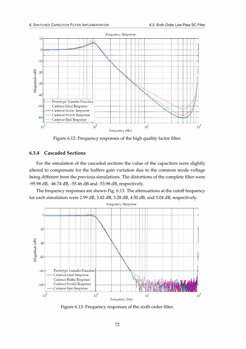
6. SWITCHED CAPACITOR FILTER IMPLEMENTATION 6.3. Sixth-Order Low-Pass SC Filter
Figure 6.12: Frequency responses of the high quality factor filter.
6.3.4 Cascaded Sections
For the simulation of the cascaded sections the value of the capacitors were slightlyaltered to compensate for the buffers gain variation due to the common mode voltagebeing different from the previous simulations. The distortions of the complete filter were-95.98 dB, -46.74 dB, -55.46 dB and -53.98 dB, respectively.
The frequency responses are shown Fig. 6.13. The attenuations at the cutoff frequencyfor each simulation were 2.99 dB, 3.82 dB, 3.28 dB, 4.50 dB, and 3.04 dB, respectively.
Figure 6.13: Frequency responses of the sixth-order filter.
72
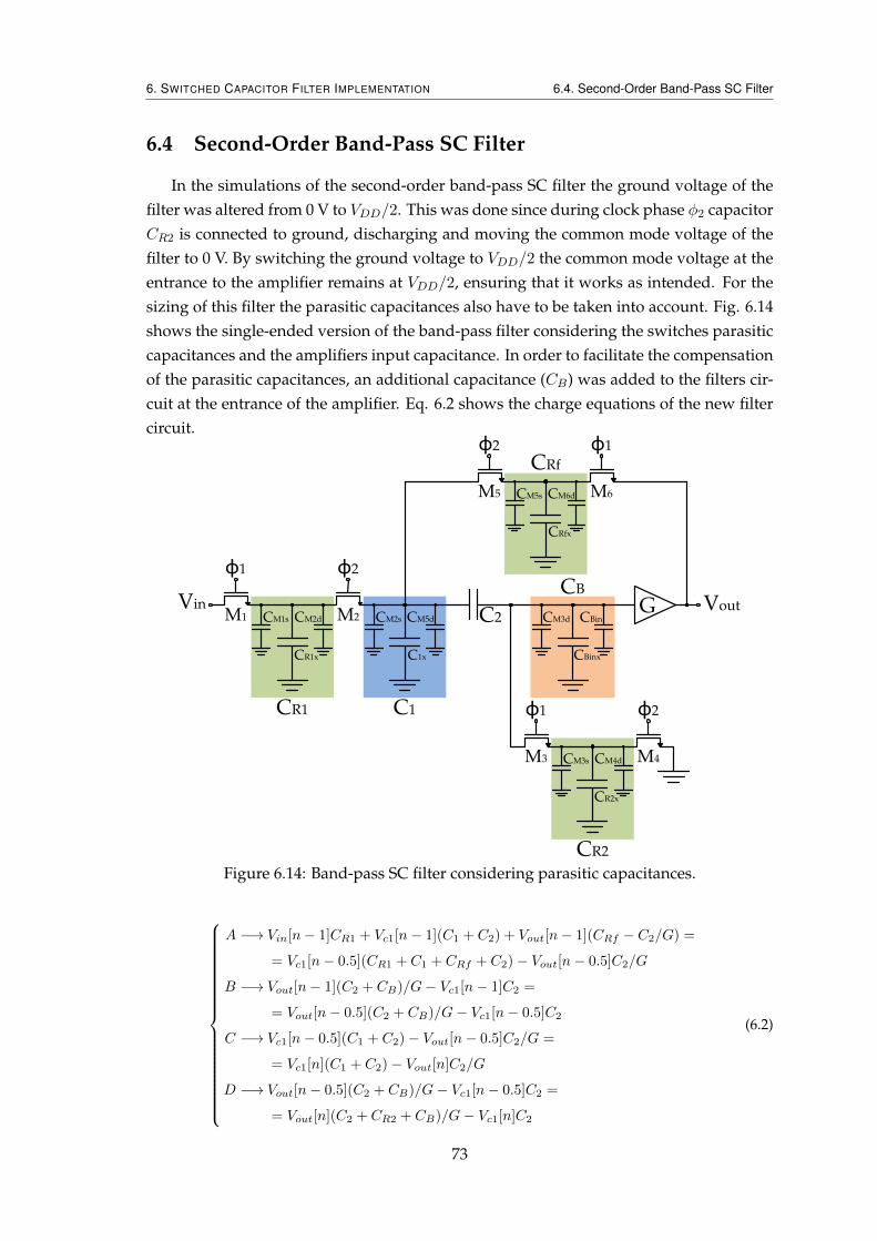
6. SWITCHED CAPACITOR FILTER IMPLEMENTATION 6.4. Second-Order Band-Pass SC Filter
6.4 Second-Order Band-Pass SC Filter
In the simulations of the second-order band-pass SC filter the ground voltage of thefilter was altered from 0 V to VDD/2. This was done since during clock phase φ2 capacitorCR2 is connected to ground, discharging and moving the common mode voltage of thefilter to 0 V. By switching the ground voltage to VDD/2 the common mode voltage at theentrance to the amplifier remains at VDD/2, ensuring that it works as intended. For thesizing of this filter the parasitic capacitances also have to be taken into account. Fig. 6.14shows the single-ended version of the band-pass filter considering the switches parasiticcapacitances and the amplifiers input capacitance. In order to facilitate the compensationof the parasitic capacitances, an additional capacitance (CB) was added to the filters cir-cuit at the entrance of the amplifier. Eq. 6.2 shows the charge equations of the new filtercircuit.
C1
Vin
φ1
CR1x
CM1sM1
φ2
M2CM2d
CR1
CM2s
C1x
CM5d C2
CBinx
CM3d
φ1
CR2x
CM3sM3
φ2
M4CM4d
CR2
φ2
CRfx
CM5sM5
φ1
M6CM6d
CRf
CBVoutG
CBin
Figure 6.14: Band-pass SC filter considering parasitic capacitances.
A −→ Vin[n− 1]CR1 + Vc1[n− 1](C1 + C2) + Vout[n− 1](CRf − C2/G) =
= Vc1[n− 0.5](CR1 + C1 + CRf + C2)− Vout[n− 0.5]C2/G
B −→ Vout[n− 1](C2 + CB)/G− Vc1[n− 1]C2 =
= Vout[n− 0.5](C2 + CB)/G− Vc1[n− 0.5]C2
C −→ Vc1[n− 0.5](C1 + C2)− Vout[n− 0.5]C2/G =
= Vc1[n](C1 + C2)− Vout[n]C2/G
D −→ Vout[n− 0.5](C2 + CB)/G− Vc1[n− 0.5]C2 =
= Vout[n](C2 + CR2 + CB)/G− Vc1[n]C2
(6.2)
73
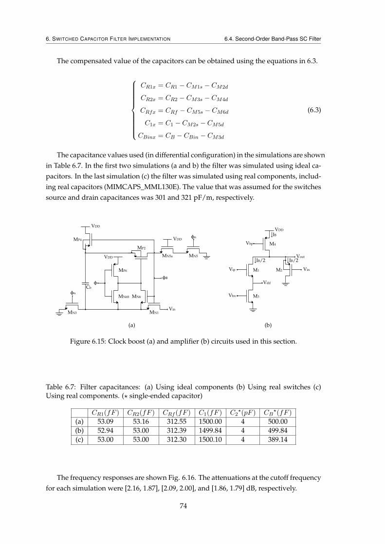
6. SWITCHED CAPACITOR FILTER IMPLEMENTATION 6.4. Second-Order Band-Pass SC Filter
The compensated value of the capacitors can be obtained using the equations in 6.3.
CR1x = CR1 − CM1s − CM2d
CR2x = CR2 − CM3s − CM4d
CRfx = CRf − CM5s − CM6d
C1x = C1 − CM2s − CM5d
CBinx = CB − CBin − CM3d
(6.3)
The capacitance values used (in differential configuration) in the simulations are shownin Table 6.7. In the first two simulations (a and b) the filter was simulated using ideal ca-pacitors. In the last simulation (c) the filter was simulated using real components, includ-ing real capacitors (MIMCAPS_MML130E). The value that was assumed for the switchessource and drain capacitances was 301 and 321 pF/m, respectively.
φ
φn
Vin
VDD
VDD
VDD
Cb
MN5a MN5
MN1
MN6S MN6
MP6
MP2
MP4
φB
φn
MN3
(a)
IB
VDD
Vbp
Vout
Vin
IB/2
M1Vip
IB/2
M3Vbn
M4
M2
Vdif
(b)
Figure 6.15: Clock boost (a) and amplifier (b) circuits used in this section.
Table 6.7: Filter capacitances: (a) Using ideal components (b) Using real switches (c)Using real components. (? single-ended capacitor)
CR1(fF ) CR2(fF ) CRf (fF ) C1(fF ) C2?(pF ) CB
?(fF )
(a) 53.09 53.16 312.55 1500.00 4 500.00(b) 52.94 53.00 312.39 1499.84 4 499.84(c) 53.00 53.00 312.30 1500.10 4 389.14
The frequency responses are shown Fig. 6.16. The attenuations at the cutoff frequencyfor each simulation were [2.16, 1.87], [2.09, 2.00], and [1.86, 1.79] dB, respectively.
74
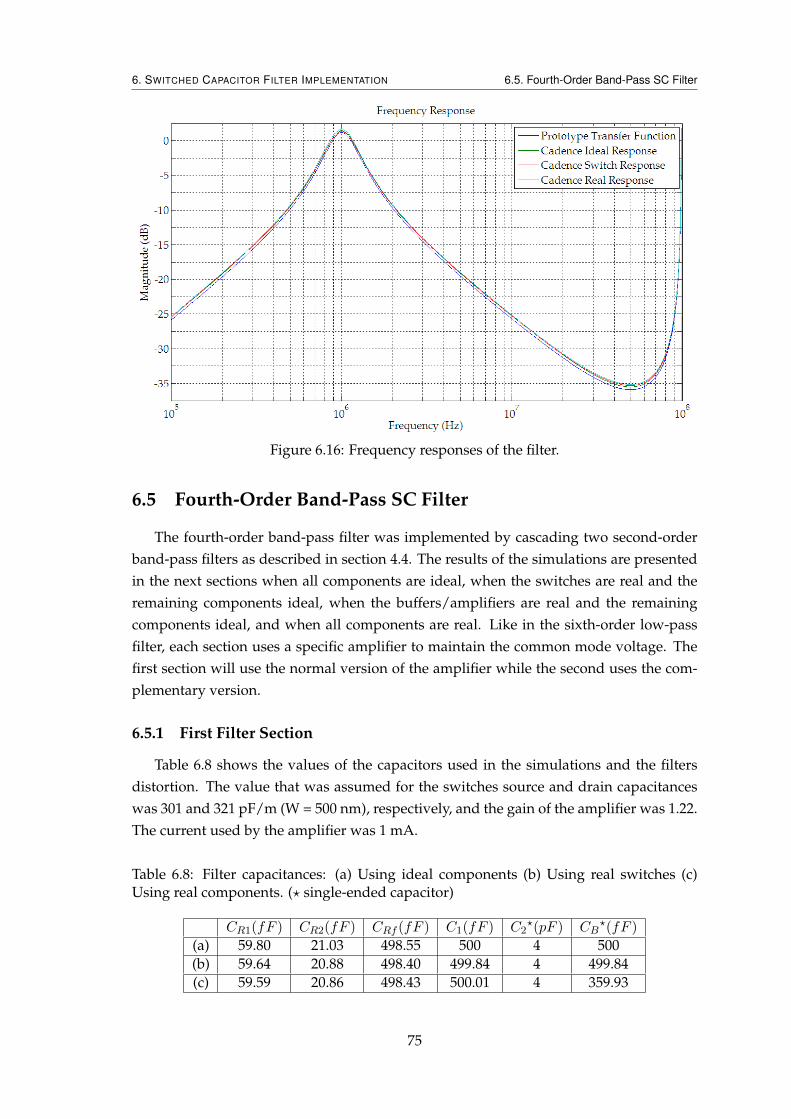
6. SWITCHED CAPACITOR FILTER IMPLEMENTATION 6.5. Fourth-Order Band-Pass SC Filter
Figure 6.16: Frequency responses of the filter.
6.5 Fourth-Order Band-Pass SC Filter
The fourth-order band-pass filter was implemented by cascading two second-orderband-pass filters as described in section 4.4. The results of the simulations are presentedin the next sections when all components are ideal, when the switches are real and theremaining components ideal, when the buffers/amplifiers are real and the remainingcomponents ideal, and when all components are real. Like in the sixth-order low-passfilter, each section uses a specific amplifier to maintain the common mode voltage. Thefirst section will use the normal version of the amplifier while the second uses the com-plementary version.
6.5.1 First Filter Section
Table 6.8 shows the values of the capacitors used in the simulations and the filtersdistortion. The value that was assumed for the switches source and drain capacitanceswas 301 and 321 pF/m (W = 500 nm), respectively, and the gain of the amplifier was 1.22.The current used by the amplifier was 1 mA.
Table 6.8: Filter capacitances: (a) Using ideal components (b) Using real switches (c)Using real components. (? single-ended capacitor)
CR1(fF ) CR2(fF ) CRf (fF ) C1(fF ) C2?(pF ) CB
?(fF )
(a) 59.80 21.03 498.55 500 4 500(b) 59.64 20.88 498.40 499.84 4 499.84(c) 59.59 20.86 498.43 500.01 4 359.93
75
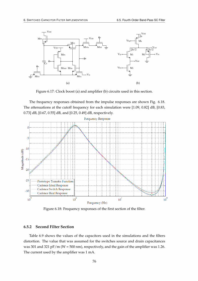
6. SWITCHED CAPACITOR FILTER IMPLEMENTATION 6.5. Fourth-Order Band-Pass SC Filter
φ
φn
Vin
VDD
VDD
VDD
Cb
MN5a MN5
MN1
MN6S MN6
MP6
MP2
MP4
φB
φn
MN3
(a)
IB
VDD
Vbp
Vout
Vin
IB/2
M1Vip
IB/2
M3Vbn
M4
M2
Vdif
(b)
Figure 6.17: Clock boost (a) and amplifier (b) circuits used in this section.
The frequency responses obtained from the impulse responses are shown Fig. 6.18.The attenuations at the cutoff frequency for each simulation were [1.09, 0.82] dB, [0.83,0.73] dB, [0.67, 0.55] dB, and [0.25, 0.49] dB, respectively.
Figure 6.18: Frequency responses of the first section of the filter.
6.5.2 Second Filter Section
Table 6.9 shows the values of the capacitors used in the simulations and the filtersdistortion. The value that was assumed for the switches source and drain capacitanceswas 301 and 321 pF/m (W = 500 nm), respectively, and the gain of the amplifier was 1.26.The current used by the amplifier was 1 mA.
76
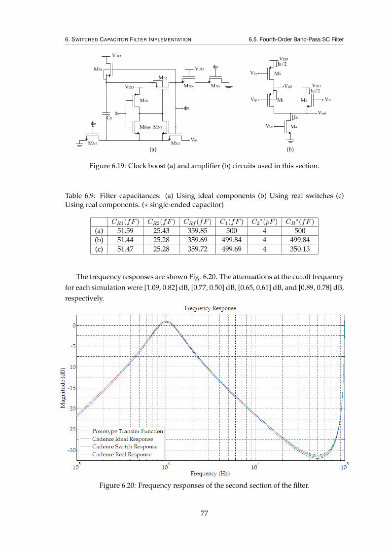
6. SWITCHED CAPACITOR FILTER IMPLEMENTATION 6.5. Fourth-Order Band-Pass SC Filter
φ
φn
Vin
VDD
VDD
VDD
Cb
MN5a MN5
MN1
MN6S MN6
MP6
MP2
MP4
φB
φn
MN3
(a)
Vbp
Vip
IB/2VDD
M3
M4Vbn
IB
M2 Vin
VDD
IB/2
Vout
M1
Vdif
(b)
Figure 6.19: Clock boost (a) and amplifier (b) circuits used in this section.
Table 6.9: Filter capacitances: (a) Using ideal components (b) Using real switches (c)Using real components. (? single-ended capacitor)
CR1(fF ) CR2(fF ) CRf (fF ) C1(fF ) C2?(pF ) CB
?(fF )
(a) 51.59 25.43 359.85 500 4 500(b) 51.44 25.28 359.69 499.84 4 499.84(c) 51.47 25.28 359.72 499.69 4 350.13
The frequency responses are shown Fig. 6.20. The attenuations at the cutoff frequencyfor each simulation were [1.09, 0.82] dB, [0.77, 0.50] dB, [0.65, 0.61] dB, and [0.89, 0.78] dB,respectively.
Figure 6.20: Frequency responses of the second section of the filter.
77
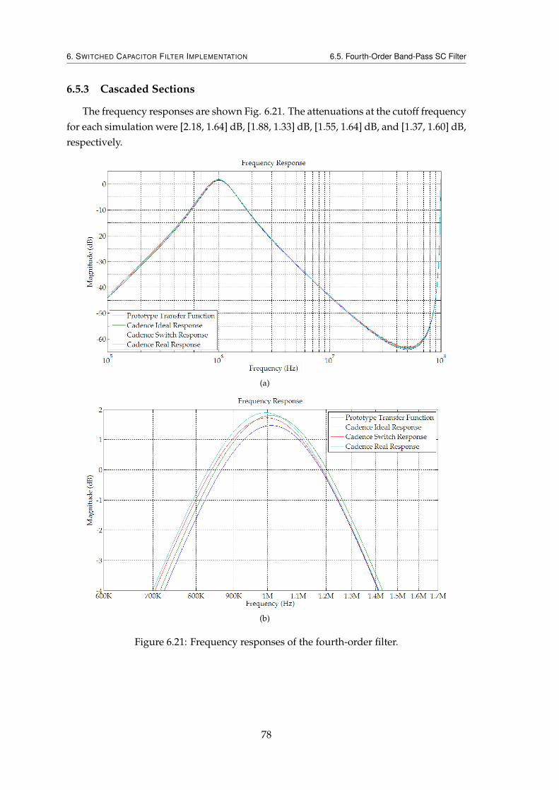
6. SWITCHED CAPACITOR FILTER IMPLEMENTATION 6.5. Fourth-Order Band-Pass SC Filter
6.5.3 Cascaded Sections
The frequency responses are shown Fig. 6.21. The attenuations at the cutoff frequencyfor each simulation were [2.18, 1.64] dB, [1.88, 1.33] dB, [1.55, 1.64] dB, and [1.37, 1.60] dB,respectively.
(a)
(b)
Figure 6.21: Frequency responses of the fourth-order filter.
78
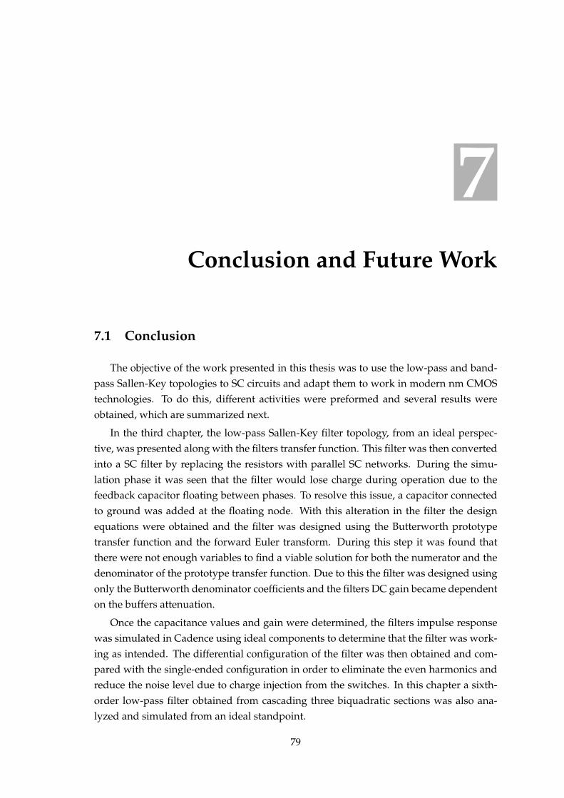
7Conclusion and Future Work
7.1 Conclusion
The objective of the work presented in this thesis was to use the low-pass and band-pass Sallen-Key topologies to SC circuits and adapt them to work in modern nm CMOStechnologies. To do this, different activities were preformed and several results wereobtained, which are summarized next.
In the third chapter, the low-pass Sallen-Key filter topology, from an ideal perspec-tive, was presented along with the filters transfer function. This filter was then convertedinto a SC filter by replacing the resistors with parallel SC networks. During the simu-lation phase it was seen that the filter would lose charge during operation due to thefeedback capacitor floating between phases. To resolve this issue, a capacitor connectedto ground was added at the floating node. With this alteration in the filter the designequations were obtained and the filter was designed using the Butterworth prototypetransfer function and the forward Euler transform. During this step it was found thatthere were not enough variables to find a viable solution for both the numerator and thedenominator of the prototype transfer function. Due to this the filter was designed usingonly the Butterworth denominator coefficients and the filters DC gain became dependenton the buffers attenuation.
Once the capacitance values and gain were determined, the filters impulse responsewas simulated in Cadence using ideal components to determine that the filter was work-ing as intended. The differential configuration of the filter was then obtained and com-pared with the single-ended configuration in order to eliminate the even harmonics andreduce the noise level due to charge injection from the switches. In this chapter a sixth-order low-pass filter obtained from cascading three biquadratic sections was also ana-lyzed and simulated from an ideal standpoint.
79
7. CONCLUSION AND FUTURE WORK 7.1. Conclusion
In the fourth chapter, the band-pass Sallen-Key filter topology, from an ideal per-spective, was presented and the same steps from the previous chapter were taken. Thistopology, however, did not have problems of floating capacitors, but due to capacitorCR2 discharging to ground during clock phase φ2 the common mode voltage of the fil-ter was lost. To avoid loosing the common mode voltage, the capacitor was connectedto VDD/2 during clock phase φ2. Unlike the low-pass version, the band-pass filter wasdesigned using both the numerator and the denominator of the prototype transfer func-tion. In the simulation using real components, the filter had a small gain over the pro-totype frequency response. A fourth-order band-pass filter obtained from cascading twobiquadratic sections was also analyzed and simulated from an ideal standpoint.
In the fifth chapter, the non-ideal effects of using real components was studied. Threetypes of switches were simulated in a first-order SC filter, to determine which one of-fered the best performance in terms of harmonic distortion. From the simulations it wasdetermined that increasing the width of the switches reduces the non-linear effects intro-duced by the switches resistance, but increasing the width of the switches increases thenon-linear effects of the parasitic capacitances, increasing the difficulty in compensatingthem during the design phase. Overall, it was determined that a NMOS switch driven bya boosted clock signal offers the best performance when narrow switches are used. Twoclock boost circuits were presented and simulated, one for regular 1.2 V operation andone for operation at both 1.2 V and 0.9 V. For this second clock boost circuit it was deter-mined that the minimum supply voltage at which this circuit correctly operates dependson the clock frequency. If the clock frequency is increased beyond the circuit bandwidththe phases will overlap and cannot be used in the SC filters.
The non-ideal effects of buffers were also analyzed in the fifth chapter. Two bufferswere analyzed (DC gain, thermal noise referred to the input, and transfer function) intheir normal and in their complementary configuration. This was done to allow the cas-cading the biquadratic sections and maintain the common mode voltage away from theground and supply voltages, since signals begin to saturate close to these voltages in-creasing the harmonic distortion they introduce in the filter. In the complementary con-figuration of the source follower with gds compensation, which is used in the low-passfilters, it was seen that the gain of the circuit was lower than the normal configurationdue to the body effect in one of the transistors. To compensate the body effect, RF tran-sistor models were used in both configurations since both NMOS and PMOS devices canconnect their bulks and sources together, when using these models, eliminating the bodyeffect and improving the buffers gain. To improve the harmonic distortion introduced bythese buffers, the common mode voltage was adjusted from VDD/2 to (VDD − VGS1)/2 sothat the common mode voltage value of both the input and output signal stay as far awayas possible from the supply voltage and ground. Using this technique the harmonic dis-tortion improved in over 10 dB. Two configurations of the fully-differential voltage com-biner were also analyzed. This amplifier is used in the band-pass filter since it has a gain
80
7. CONCLUSION AND FUTURE WORK 7.2. Future Work
higher than 1 and is also used in the low-voltage low-pass filter with source degenera-tion to improve the differential pairs linearity at the cost of losing gain. Using the sourcedegeneration technique it was possible to improve the amplifiers harmonic distortion byover 10 dB.
In the seventh chapter, several filters were simulated: when all components are ideal,when the switches are real and the remaining components ideal, when the buffers/am-plifiers are real and the remaining components ideal, and when all components are realin order to determine the influence of each non-ideal component in the frequency re-sponse of the filter. From the simulation it was concluded that the buffer/amplifier isthe element of the filter responsible for introducing the most distortion. While the out-put capacitance of the buffer/amplifier can be neglected, the input capacitance must becompensated during the design phase of the filter. In the band-pass filter, to facilitate thecompensation of the amplifiers input capacitance, a new capacitance was added to thefilters circuit, and the design equations were recalculated. During the simulation of thesixth-order low-pass filter it was determined that when using high quality factors, thefilter is more sensitive to component variations and thus more susceptible to the compo-nents non-linearities.
7.2 Future Work
Following the work done in this thesis new investigation topics emerged from theresults obtained. Some of these objectives are described below.
Improve the overall performance of the filter:
While the distortion obtained from simulations of the low-pass filters varied between-55 and -68 dB, these results can be improved further. In terms of switches, the distortionthey introduce in the filter can be further reduced using clock boosting circuits whichdrive them depending on the switches input voltage. This, however, will require thestudy and compensation of the input parasitic capacitances of the clock boost circuit,since they will influence the filter performance.
Other techniques and/or buffers and low gain amplifiers circuits should be studied inorder to improve the performance of these circuits. In this work the buffer and amplifierwere the elements which introduced most distortion in the filter. The input parasitic ca-pacitances of these circuits should be taken into account, since their non-linear variationwill affect the performance of the filter.
Development of a systematic design methodology:
Development of a systematic design methodology, based on genetic algorithms, toobtain the best possible performance of a given circuit taking into consideration all thedesign variables.
81
7. CONCLUSION AND FUTURE WORK
Research of other SC circuit topologies:
Research and study other SC circuit topologies suitable to implement filtering func-tions using voltage buffers or low gain amplifiers, specifically circuit topologies that al-low the implementation of bilinear transform based filters should be investigated, sincethey do not require clock frequencies as high as the Euler transforms.
82
AButterworth Filtering Transfer
Function
A.1 Continuous-Time Low-Pass Butterworth Transfer Function
In order to obtain the values for the components in a filter, using the circuits transferfunction, a prototype transfer function must be used. In this section it is described howto obtain the numeric values for the coefficients of the transfer function, using the But-terworth prototype transfer function. This transfer function can be obtained in severalways. It is possible to use a software tool, such as Matlab, to determine the prototypetransfer function. In this case, it is necessary to indicate the order of the filter N and thedesired cutoff frequency ωp in [rad/s] (Table A.1), where n and d represent the values forthe coefficients of the numerator and the denominator, respectively.
Table A.1: Obtaining the Butterworth transfer function coefficients using Matlab for acontinuous-time low-pass filter.
[n,d]=butter(N,ωp,’s’)
Alternatively, the filter can be designed using the mathematical equations first em-ployed by S. Butterworth [SS04]. Using these equations, besides specifying the order ofthe filter and the cutoff frequency, it is also necessary to select the desired attenuationAmax at the cutoff frequency. The previous parameter is used to calculate the value of εwhich is necessary to obtain the coefficients of the transfer function. The equation in Eq.A.1 shows how ε is calculated.
ε =
√10
Amax10 − 1 (A.1)
83
A. BUTTERWORTH FILTERING TRANSFER FUNCTION
When the order of the filter is known, one of the equations in Eq. A.2 can be usedto determine the denominator of the prototype transfer function [GK71], where Bn is thedenominator of the normalized prototype transfer function, and S is the normalized s
plane.
Bn(S) =
n2∏
k=1
[S2 − 2 S cos
(π
2k + n− 1
2n
)+ 1
]for even n
Bn(S) = (S + 1)
n−12∏
k=1
[S2 − 2 S cos
(π
2k + n− 1
2n
)+ 1
]for odd n
(A.2)
A.1.1 First-Order prototype transfer function
To implement a first-order filter, using Eq. A.2 with n = 1, the normalized prototypetransfer function (Eq. A.3) is obtained.
T (S) =1
S + 1(A.3)
Depending on the type of filter (low-pass, band-pass, high-pass) the variable S isreplaced with certain coefficients. To implement a low-pass filter, using Eq. A.3 with thelow-pass coefficients, the first-order low-pass filter prototype transfer function (Eq. A.4)is obtained.
T
(S =
s
ωpε
1N
)=
ωp
ωp + ε1N s
(A.4)
A.1.2 Second-Order prototype transfer function
To implement a second-order filter, using Eq. A.2 with n = 2, the normalized pro-totype transfer function (Eq. A.5) is obtained. This means that the quality factor for asecond-order Butterworth filter is Qp = 1/1.4142 = 1/
√2 =√
2/2.
T (S) =1
S2 + 1.4142S + 1(A.5)
Using Eq. A.5 with the low-pass coefficients, the second-order low-pass filter proto-type transfer function (Eq. A.6) is obtained.
T
(S =
s
ωpε
1N
)=
ω2p
ω2p +
ωpε1N
Qps+ ε
2N s2
(A.6)
Using either software tools or the Butterworth mathematical equations, the coeffi-cients for the prototype transfer functions can be obtained. Since usually there are more
84
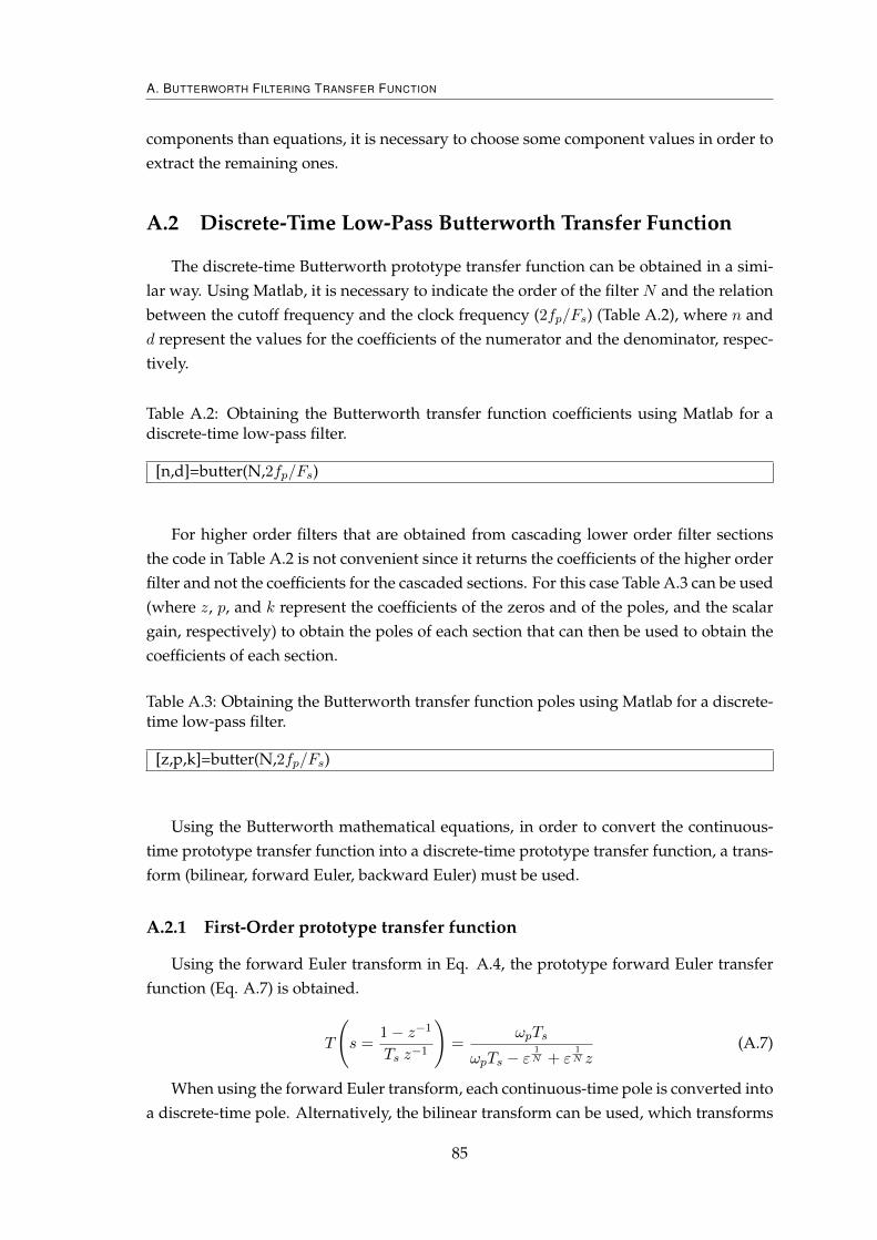
A. BUTTERWORTH FILTERING TRANSFER FUNCTION
components than equations, it is necessary to choose some component values in order toextract the remaining ones.
A.2 Discrete-Time Low-Pass Butterworth Transfer Function
The discrete-time Butterworth prototype transfer function can be obtained in a simi-lar way. Using Matlab, it is necessary to indicate the order of the filter N and the relationbetween the cutoff frequency and the clock frequency (2fp/Fs) (Table A.2), where n andd represent the values for the coefficients of the numerator and the denominator, respec-tively.
Table A.2: Obtaining the Butterworth transfer function coefficients using Matlab for adiscrete-time low-pass filter.
[n,d]=butter(N,2fp/Fs)
For higher order filters that are obtained from cascading lower order filter sectionsthe code in Table A.2 is not convenient since it returns the coefficients of the higher orderfilter and not the coefficients for the cascaded sections. For this case Table A.3 can be used(where z, p, and k represent the coefficients of the zeros and of the poles, and the scalargain, respectively) to obtain the poles of each section that can then be used to obtain thecoefficients of each section.
Table A.3: Obtaining the Butterworth transfer function poles using Matlab for a discrete-time low-pass filter.
[z,p,k]=butter(N,2fp/Fs)
Using the Butterworth mathematical equations, in order to convert the continuous-time prototype transfer function into a discrete-time prototype transfer function, a trans-form (bilinear, forward Euler, backward Euler) must be used.
A.2.1 First-Order prototype transfer function
Using the forward Euler transform in Eq. A.4, the prototype forward Euler transferfunction (Eq. A.7) is obtained.
T
(s =
1− z−1
Ts z−1
)=
ωpTs
ωpTs − ε1N + ε
1N z
(A.7)
When using the forward Euler transform, each continuous-time pole is converted intoa discrete-time pole. Alternatively, the bilinear transform can be used, which transforms
85
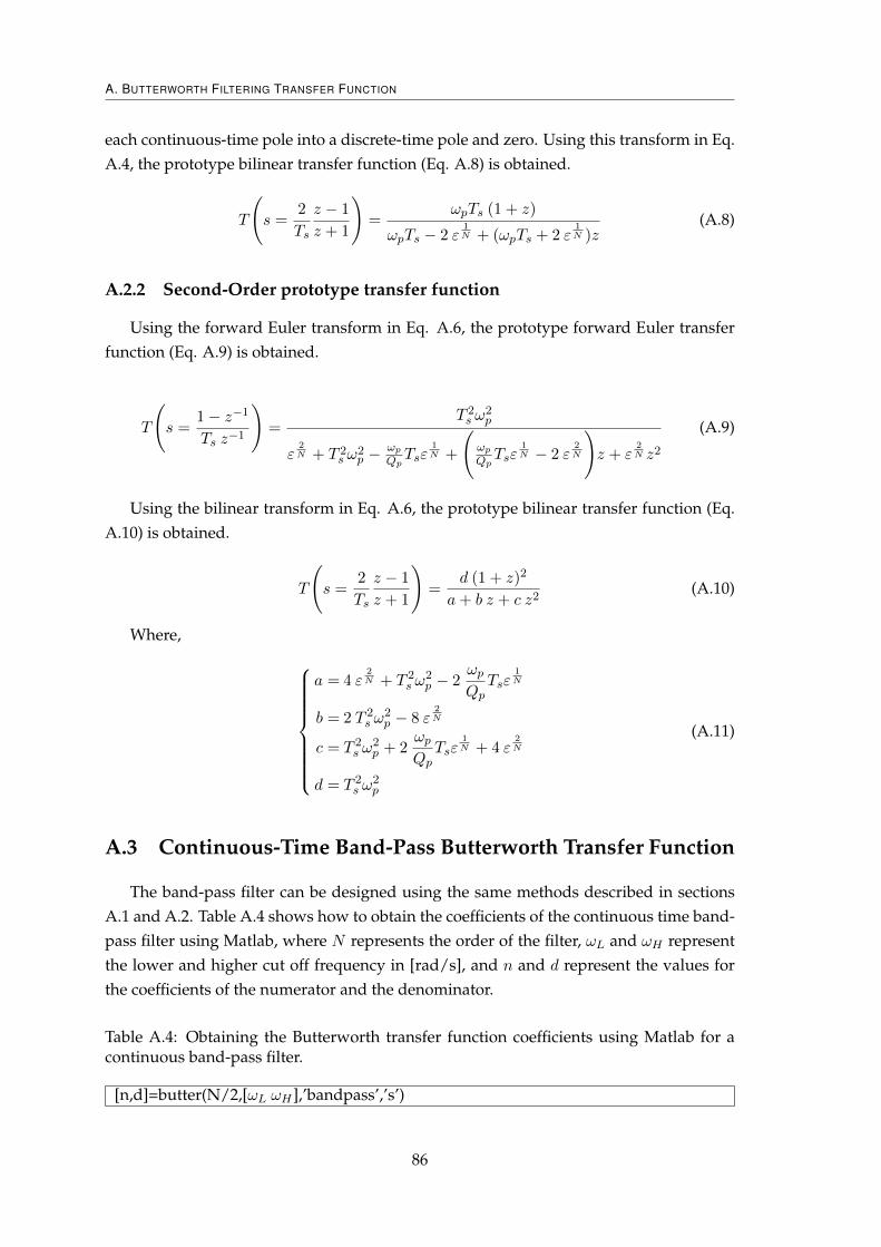
A. BUTTERWORTH FILTERING TRANSFER FUNCTION
each continuous-time pole into a discrete-time pole and zero. Using this transform in Eq.A.4, the prototype bilinear transfer function (Eq. A.8) is obtained.
T
(s =
2
Ts
z − 1
z + 1
)=
ωpTs (1 + z)
ωpTs − 2 ε1N + (ωpTs + 2 ε
1N )z
(A.8)
A.2.2 Second-Order prototype transfer function
Using the forward Euler transform in Eq. A.6, the prototype forward Euler transferfunction (Eq. A.9) is obtained.
T
(s =
1− z−1
Ts z−1
)=
T 2s ω
2p
ε2N + T 2
s ω2p −
ωp
QpTsε
1N +
(ωp
QpTsε
1N − 2 ε
2N
)z + ε
2N z2
(A.9)
Using the bilinear transform in Eq. A.6, the prototype bilinear transfer function (Eq.A.10) is obtained.
T
(s =
2
Ts
z − 1
z + 1
)=
d (1 + z)2
a+ b z + c z2(A.10)
Where,
a = 4 ε2N + T 2
s ω2p − 2
ωp
QpTsε
1N
b = 2 T 2s ω
2p − 8 ε
2N
c = T 2s ω
2p + 2
ωp
QpTsε
1N + 4 ε
2N
d = T 2s ω
2p
(A.11)
A.3 Continuous-Time Band-Pass Butterworth Transfer Function
The band-pass filter can be designed using the same methods described in sectionsA.1 and A.2. Table A.4 shows how to obtain the coefficients of the continuous time band-pass filter using Matlab, where N represents the order of the filter, ωL and ωH representthe lower and higher cut off frequency in [rad/s], and n and d represent the values forthe coefficients of the numerator and the denominator.
Table A.4: Obtaining the Butterworth transfer function coefficients using Matlab for acontinuous band-pass filter.
[n,d]=butter(N/2,[ωL ωH ],’bandpass’,’s’)
86
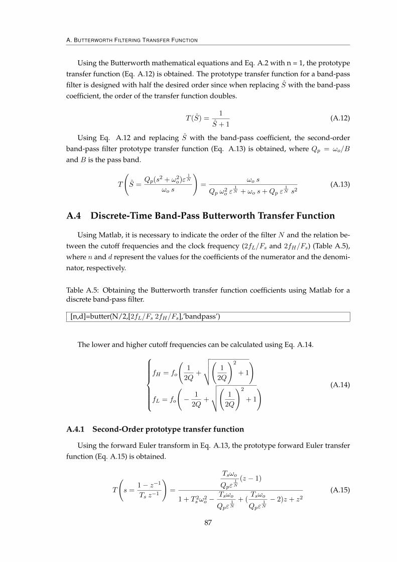
A. BUTTERWORTH FILTERING TRANSFER FUNCTION
Using the Butterworth mathematical equations and Eq. A.2 with n = 1, the prototypetransfer function (Eq. A.12) is obtained. The prototype transfer function for a band-passfilter is designed with half the desired order since when replacing S with the band-passcoefficient, the order of the transfer function doubles.
T (S) =1
S + 1(A.12)
Using Eq. A.12 and replacing S with the band-pass coefficient, the second-orderband-pass filter prototype transfer function (Eq. A.13) is obtained, where Qp = ωo/B
and B is the pass band.
T
(S =
Qp(s2 + ω2
o)ε1N
ωo s
)=
ωo s
Qp ω2o ε
1N + ωo s+Qp ε
1N s2
(A.13)
A.4 Discrete-Time Band-Pass Butterworth Transfer Function
Using Matlab, it is necessary to indicate the order of the filter N and the relation be-tween the cutoff frequencies and the clock frequency (2fL/Fs and 2fH/Fs) (Table A.5),where n and d represent the values for the coefficients of the numerator and the denomi-nator, respectively.
Table A.5: Obtaining the Butterworth transfer function coefficients using Matlab for adiscrete band-pass filter.
[n,d]=butter(N/2,[2fL/Fs 2fH/Fs],’bandpass’)
The lower and higher cutoff frequencies can be calculated using Eq. A.14.fH = fo
(1
2Q+
√√√√( 1
2Q
)2
+ 1
)
fL = fo
(− 1
2Q+
√√√√( 1
2Q
)2
+ 1
) (A.14)
A.4.1 Second-Order prototype transfer function
Using the forward Euler transform in Eq. A.13, the prototype forward Euler transferfunction (Eq. A.15) is obtained.
T
(s =
1− z−1
Ts z−1
)=
Tsωo
Qpε1N
(z − 1)
1 + T 2s ω
2o −
Tsωo
Qpε1N
+ (Tsωo
Qpε1N
− 2)z + z2(A.15)
87
A. BUTTERWORTH FILTERING TRANSFER FUNCTION
Using the bilinear transform in Eq. A.13, the prototype bilinear transfer function (Eq.A.16) is obtained.
T
(s =
2
Ts
z − 1
z + 1
)=
d (z2 − 1)
a+ b z + c z2(A.16)
Where,
a = − 2 Tsωo + 4Qpε1N +QpT
2s ω
2oε
1N
b = − 8Qpε1N + 2QpT
2s ω
2oε
1N
c = 2 Tsωo + 4Qpε1N +QpT
2s ω
2oε
1N
d = 2 Tsωo
(A.17)
88
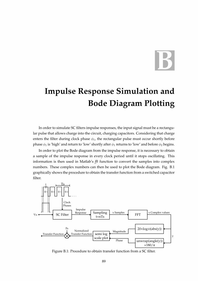
BImpulse Response Simulation and
Bode Diagram Plotting
In order to simulate SC filters impulse responses, the input signal must be a rectangu-lar pulse that allows charge into the circuit, charging capacitors. Considering that chargeenters the filter during clock phase φ1, the rectangular pulse must occur shortly beforephase φ1 is ’high’ and return to ’low’ shortly after φ1 returns to ’low’ and before φ2 begins.
In order to plot the Bode diagram from the impulse response, it is necessary to obtaina sample of the impulse response in every clock period until it stops oscillating. Thisinformation is then used in Matlab’s fft function to convert the samples into complexnumbers. These complex numbers can then be used to plot the Bode diagram. Fig. B.1graphically shows the procedure to obtain the transfer function from a switched capacitorfilter.
φ1 φ1φ2 φ2
SC FilterVin
Clock Phases
Impulse Response Sampling
t+nTs
t
x SamplesFFT
x Complex values
20×log10(abs(y))
y
unwrap(angle(y))×180/π
Magnitude
Phase
Fs
semi logscale plot
Normalized Transfer FunctionTransfer Function
Ts
Figure B.1: Procedure to obtain transfer function from a SC filter.
89
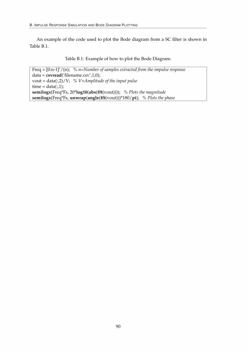
B. IMPULSE RESPONSE SIMULATION AND BODE DIAGRAM PLOTTING
An example of the code used to plot the Bode diagram from a SC filter is shown inTable B.1.
Table B.1: Example of how to plot the Bode Diagram.
Freq = [0:n-1]’/(n); % n=Number of samples extracted from the impulse responsedata = csvread(’filename.csv’,1,0);vout = data(:,2)/V; % V=Amplitude of the input pulsetime = data(:,1);semilogx(Freq*Fs, 20*log10(abs(fft(vout)))); % Plots the magnitudesemilogx(Freq*Fs, unwrap(angle(fft(vout)))*180/pi); % Plots the phase
90
Bibliography
[ACJ+06] L. Acosta, R. G. Carvajal, M. Jimenez, J. Ramirez-Angulo, and A. Loper-Martin. A CMOS transconductor with 90 dB SFDR and low sensitivity tomismatch. In IEEE Int. Symp. on Circuits and Systems (ISCAS 2006), pages 69–72, May. 2006.
[AH02] P.E. Allen and D.R. Holberg. CMOS Analog Circuit Design. The Oxford Seriesin Electrical and Computer Engineering. Oxford University Press, USA, 2002.
[CJM12] T.C. Carusone, D.A. Johns, and K.W. Martin. Analog Integrated Circuit Design.Wiley Desktop Editions. John Wiley & Sons, 2012.
[CRCR77] J. T. Caves, S. D. Rosenbaum, M. A. Copeland, and C. F. Rahim. Sampledanalog filtering using switched-capacitors as resistors equivalents. In IEEE J.Solid State Circuits, volume SC-12, no. 6, pages 592–599, Dec. 1977.
[DK99] M. Dessouky and A. Kaiser. Input switch configuration suitable for rail-to-railoperation of switched opamp circuits. In Electronics Letters, volume 35, no. 1,pages 8–10, Jan. 1999.
[GK71] R. M. Golden and J. F. Kaiser. Root and delay parameters for normalizedbessel and butterworth low-pass transfer functions. In IEEE Trans. Audio andElectroacoustics, volume AU-19, no. 1, pages 64–71, Mar. 1971.
[GPP06] A. D. Grasso, G. Palumbo, and S. Pennisi. Three-stage CMOS OTA for largecapacitive loads with efficient frequency compensation scheme. In IEEE Trans.Circuits and Systems II: Express Briefs, volume 53, no. 10, pages 1044–1048, Oct.2006.
[GT86] Roubik Gregorian and G.C. Temes. Analog MOS integrated circuits for signalprocessing. Wiley series on filters. Wiley, 1986.
[HBG77] B. J. Hosticka, R. W. Brodersen, and P. R. Gray. MOS sampled data recur-sive filters using switched capacitor integrators. In IEEE J. Solid State Circuits,volume SC-12, no. 6, pages 600–608, Dec. 1977.
91
BIBLIOGRAPHY
[KJ88] F. Krummenacher and N. Joehl. A 4-MHz CMOS continuous-time filter withon-chip automatic tuning. In IEEE J. Solid-State Circuits, volume 23, no. 3,pages 750–758, Jun. 1988.
[KL01] Ko-Chi Kuo and A. Leuciuc. A linear MOS transconductor using source de-generation and adaptive biasing. In IEEE Trans. Circuits and Systems II: Analogand Digital Signal Processing, volume 48, no. 10, pages 937–943, Oct. 2001.
[Mar80] K. Martin. Improved circuits for the realization of switched-capacitor filters.In IEEE Trans. Circuits and Systems, volume SC-27, no. 4, pages 237–244, Apr.1980.
[MS12] F. Michel and M.S.J. Steyaert. A 250 mV 7.5 µW 61 dB SNDR SC ∆Σ modulatorusing near-threshold-voltage-biased inverter amplifiers in 130 nm CMOS. InIEEE J. Solid-State Circuits, volume 47, no. 3, pages 709–721, Mar. 2012.
[Raz01] Behzad Razavi. Design of Analog CMOS Integrated Circuits. McGraw-Hill, Inc.,New York, USA, 2001.
[SK55] R. P. Sallen and E. L. Key. A practical method of designing RC active filters.In IRE Trans. Circuit Theory, volume CT-2, pages 74–85, Mar. 1955.
[SS04] Adel S. Sedra and Kenneth C. Smith. Microelectronic Circuits. The OxfordSeries in Electrical and Computer Engineering. Oxford University Press, USA,2004.
92