Embed Size (px)
Citation preview

Switched-Capacitor Circuit Implementations • SC Biquads: Block Diagram Representations and Implementations • SC Techniques for reduced area and high Q-filters • Other SC applications
ECE 622(ESS) 1

PRACTICAL CONSIDERATIONS FOR OP AMPS
Key op amp specifications:
•Gain
•Speed (BW)
•Supply voltages
•Output swing
•Noise
•Power
+
−
2

NON-IDEAL EFFECTS OF OP AMPS
A. FINITE DC GAIN For a two integrator biquadratic filter:
QAQ
AQ
QA
A
o
o
aoo
ooA
−≅
+=
+=
21211
1ωω
Therefore: - deviations are negligible - Q deviations can be significant
oω
B. FINITE BANDWIDTH • Bandwidth is very critical for high frequency applications
3

How to determine the GB of an Op Amp? • The required GB is a function of the clock frequency and the feedback topology around the Op Amp. • A rule of thumb to select GB requires to satisfy the following inequality: a GB T/2 > 5 or GBT> 10/a where T is the period of the clock frequency, a is the capacitor ratio between the sum of all the feedback capacitors divided by the sum of all the capacitors connected to the input terminal of the Op Amp. More details later
4

MULTI-STAGE OP AMP DESIGN A. SINGLE-ENDED CONFIGURATION • High gain • CMRR = 0 • Nested compensation trades BW for stability
B. FULLY DIFFERENTIAL CONFIGURATION • High gain • Good CMRR • Rail-to-rail output swing • Higher bandwidth (less compensation) • Requires and additional CMFB and dynamic reset 5

Noise due to the switches
• The switch noise density can be expressed as
• Because two switches are present
kTRswitch4v 2noise,sw =
vin
Vnoise Rswitch
C
Rswitch
∫ π==
BW
2total,sw RswitchC
kTRswitch4dfkTRswitch8v
CkT4v total,sw π
=or
4kT=16x10-21V2C For C=1 pF the noise level is around 70 µV C=10 pF ==> noise level is around 20 µV
6
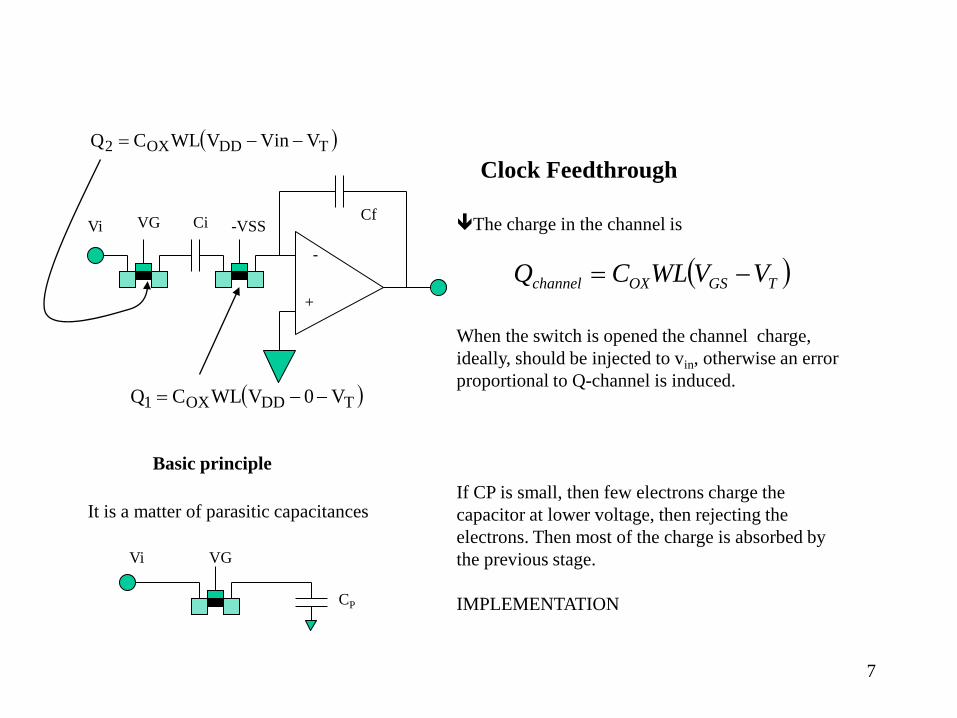
Clock Feedthrough
The charge in the channel is
When the switch is opened the channel charge, ideally, should be injected to vin, otherwise an error proportional to Q-channel is induced.
If CP is small, then few electrons charge the capacitor at lower voltage, then rejecting the electrons. Then most of the charge is absorbed by the previous stage.
IMPLEMENTATION
( )TGSOXchannel VVWLCQ −=-
+
Ci VG -VSS Vi Cf
It is a matter of parasitic capacitances
VG Vi
CP
( )TDDOX1 V0VWLCQ −−=
( )TDDOX2 VVinVWLCQ −−=
Basic principle
7
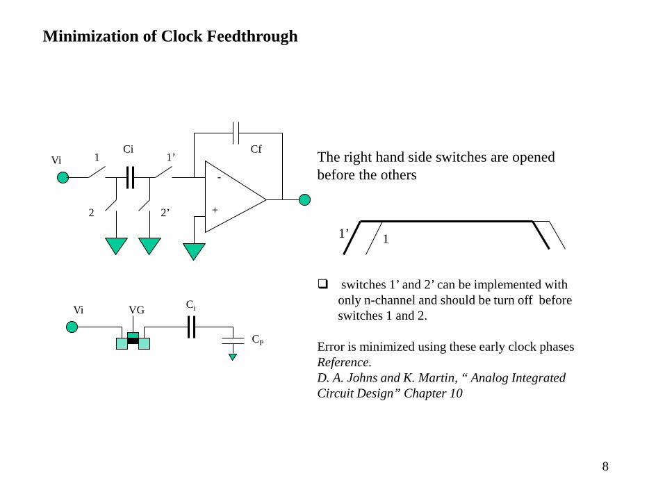
Minimization of Clock Feedthrough
The right hand side switches are opened before the others
switches 1’ and 2’ can be implemented with
only n-channel and should be turn off before switches 1 and 2.
Error is minimized using these early clock phases Reference. D. A. Johns and K. Martin, “ Analog Integrated Circuit Design” Chapter 10
-
+
Vi Cf
VG Vi
CP
1 1’
2 2’
Ci
Ci
1’ 1
8

Switch Resistance
-
+
Cf VDD VDD
vi
VSS VSS
Ci VT=VT0+∆V
Body effect
vi
Rs
( )VTVVDDWCLRs
iOXn −−µ=
Vi=VDD-VT
For VDD=1.5 V, and VT=1 ==> Vi<0.5 V !!! And for VDD=0.75 V ?
9
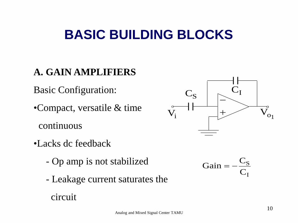
BASIC BUILDING BLOCKS
A. GAIN AMPLIFIERS
Basic Configuration:
•Compact, versatile & time
continuous
•Lacks dc feedback
- Op amp is not stabilized
- Leakage current saturates the
circuit
−+
o o
iV
IC
1oV
SC
I
SCCGain −=
Analog and Mixed Signal Center TAMU 10

Improved Gain Amplifier •Low sensitivity to the op amp
offset voltage and open loop
gain (due to charge
cancellation
•Additional capacitor between
nodes A and B eliminates the
“spikes” during the non-
overlapping clock phases I
SCCgain −=
−+
o o
iV
HC
oVSC•
1φ
2φ••
A
B
•• •
1φ
2φ
•• •
IC 1φ
2φ
11

B. Integrators Conventional stray-insensitive integrators: •Non-inverting:
•Inverting:
−+
o
iV
ICooV
SC••
o
eoVo
1φ
2φ
• •
1φ
2φ
2φ
1φ•
−+
o
iV
ICooV
SC••
o
eoVo
1φ
2φ
• •1φ
2φ2φ
1φ•
12

Type of Integrator
Mapping Transfer (Equivalent) Function
Magnitude, )e(H Tjω
Phase, )e(HA Tj
RGω
−+
• •
1V
2C
oV1R
1V
−+
• •
2C
oV1C
1φ 2φ
Inverting (Forward)
Non-Inverting
Inverting (Backward)
−+
• •
2C
oV
1C
iV• •
1φ
2φ
2φ
1φ
−+
• •
2C
oV
1C
iV• •
1φ
2φ2φ
1φ
ωωo
))2/Tsin(
2/T(
atVFor
o
2o
ωω
ωω
φ
))2/Tsin(
2/T(
atVFor
o
1o
ωω
ωω
φ
))2/Tsin(
2/T(
atVFor
o
2o
ωω
ωω
φ
))2/Tsin(
2/T(
atVFor
o
1o
ωω
ωω
φ
))2/Tsin(
2/T(
atVFor
o
2o
ωω
ωω
φ
))2/Tsin(
2/T(
atVFor
o
1o
ωω
ωω
φ
2π
2π
2T
2ω
−π
2π
−
2T
2ω
−π
−
2π
2T
2ω
+π
In the S-Plane LDI
Forward
LDI Forward
Backward
LDI
SCSR1)S(H.e.i o
21
ω−==
)Z1
Z(CC)Z(H 1
2/1
2
1−
−
−−=
)Z1
Z(CC)Z(H 1
1
2
1−
−
−−=
)Z1
Z(CC)Z(H 1
2/1
2
1−
−
−=
)Za
Z(CC)Z(H 1
1
2
1−
−
−−=
)Z1
Z(CC)Z(H 1
2/1
2
1−
−
−−=
)Z11(
CC)Z(H 1
2
1−−
−=
13

Basic SC first-order low-pass
−+
inV1R
2R
CoutV
−+inV
CoutV1C
• •1φ
2φ2φ
1φ
2C• •
1φ
2φ2φ
1φ
Active RC prototype
2
12sCR1
R/R)s(H+
−=
2,1i,fC/1C/TR Siieq ===
1)C/C1(zz)C/C()z(H
2
1−+
−=
0Zzero =
)C/C1/(1Z 2pole +=
14

Improved Integrator with reduced capacitance spread
Problem: offset Solution: use an offset & low dc gain compensated integrator as the 2nd stage (only valid for two-integrator loop applications)
−+
oinV C e
oV1C• •
1φ
2φ2φ
1φ
2C
• •
1φ
2φ
2φ
o o• •
••
3C
4C
1'42
31oin
eooe
z11
CCCC
)z(V)z(V)z(H −−
−==
34'4 CCC +=
15
Offset and gain compensated Integrator
• compensates the offset voltage and dc gain error of the op amp • eliminates spikes (providing continuous feedback to the op amp)
−+
oinV o
oV1C• •
2φ2φ
1φ
FC
o o• •
••
hC2φ1φ
MC
1F
1oin
oooo
z11
CC
)z(V)z(V)z(H −−
−==
hC
MC
16

SWITCHED-CAPACITOR FILTER IMPLEMENTATIONS
φ1 φ1φ1 φ1
C2 C3
C1 CA
φ2 φ2 φ2 φ2
Vi ooV
+ 1Z11
−−+
iVA
2
CC
−
A
3
CC
−
A
1
CC
−
i
A
3
A
1
A
21
o V
1ZCC
1
CC
ZC
CC
V
−
+
++
−=
+ 1Z11
−− 1Z11
−−+ +
1K−
2K−
3K−
4K−
1oV
15ZK −
6K−
2oV
φ2
φ1
K1C1
φ2
C1
C2
K6C2
φ1
φ1
φ1φ2 φ2
V02
φ1
φ1
φ2φ1 K5C2
V01
K4C1
φ1
φ2 φ2
K2C2φ1
φ2φ2
φ1
Vi
K3C2
φ2
17

−+
12 =C
)(out sV
11 =C
)(SVin
• Q/1
• • −+
2k
•
•
•
oω/1−
• • •
ok ω/1
oo k/ω
oω/1
An alternate realization of a general active-RC biquad filter
•
•
•
A direct mapping from an active-RC filter into a SC Filter. Since negative (equivalent) resistances are easily implemented in SC, a modified Active-RC prototype is next described
18
• 16CK
•
23CK
• •
1φ
2φ2φ
1φ
1φ
25CK
2φ1φ
•
2φ
14CK
•
)(1 ZV
)(ZVi
−+
•
• • 11CK
2φ• • •
•
1φ 1φ
2φ
12CK
• 1C
• • −+
2C
)(out ZV•
•
•
1φ
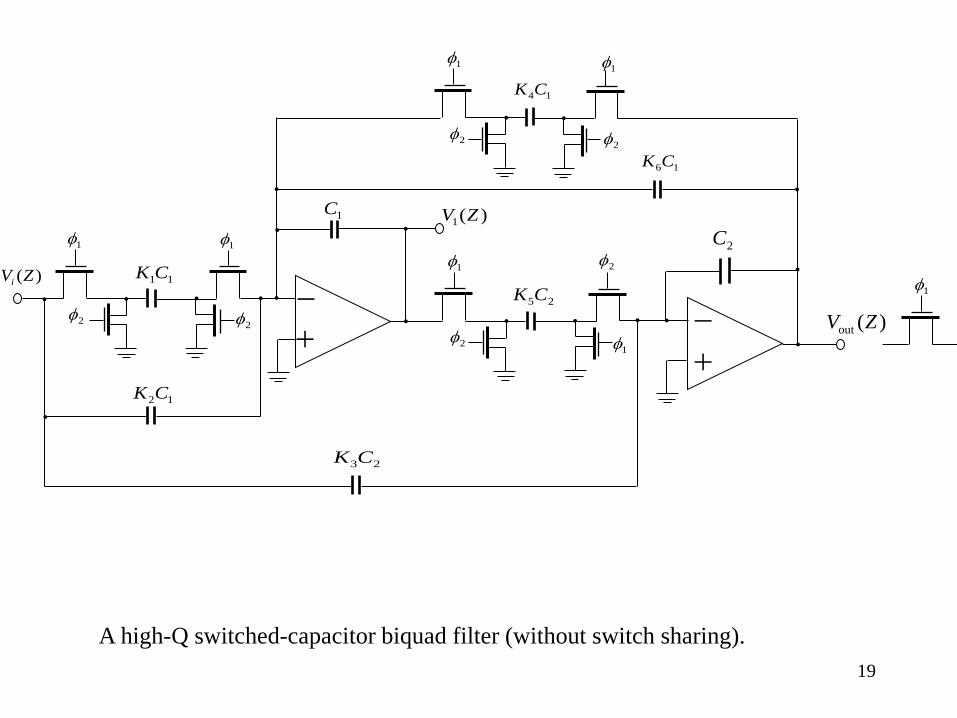
A high-Q switched-capacitor biquad filter (without switch sharing). 19

+ + outV
+ 1Z11
−− 1Z11
−−+ +
1K−
2K−
3K−
4K−
15 ZK −
6K−
outV
Vio
oKω
−
1o kω−
2k−
s1 s1+
Q−
oω−
oω
Building Block Diagrams of Figs. In p 18 and 19

Biquad Circuit & Block Diagrams
Circuit Diagram Block Diagram
−+inV
ooVAC
• •
2φ
1φ
C
o o• •
•
2φ
1φ
−+
GC• •
2φ
1φ
C
• •
2φ
1φ
•
CC• •
2φ
1φ
2φ
1φ• •
ECInverting Summer
E−
A
1
1
z1z
−
−
−∑ 1z1
1−−
o
oV∑
C−
G−o
inV
Inverting Integrators Non-inverting Integrator
21

Biquad Circuit 1
Circuit Diagram Block Diagram
−+
inV
oV
2C
o
o• •−+
1C
22Cα2φ
1φ
2φ
1φ
25Cα
2φ
1φ 2φ
1φ
17Cα
2φ
1φ 2φ
1φ
28Cα2φ
1φ
•
•••
••
•
• • •
• •
2φ 1φ
•
22

Biquad Circuit 2
Block Diagram Circuit Diagram
1F4 C/C−
2F2 C/C
1
1
z1z
−
−
−1z11
−−o
oV∑
1F3 C/C−
1F1 C/C−o
inV
23

•−+ outV
2FC
o−+
1FC
2C2
1 2
4C
21
3C21
•
•••
•
• • ••
•
11
•2
•
•hC
6 10
21
12 11
7 89
•
2•
3
21
"1FC
2
1••
4• •
'1FC
•
inVo20
2
5
SC Bandpass C Diagram
1F
4"
1F'1F
'1F
CC
CCC+
−
2F
2CC 1
1
z1z
−
−
−1z11
−−o
oV∑
1F
3CC
−
1F
1"
1F'1F
'1F
CC
CCC+
−
o
inV
•
•
SC Bandpass Filter Block Diagram 24

Capacitor Values for the SC Filter
Capacitor Values )Hz(fo )Cu(C'
1F )Cu(CC 2F1F =
697 852 1209 1477
4 2.6 1.5 1.1
11.4 9.3 6.6 5.4 ,Cu2.2C,Cu1CCCC:Where 1h432 =====
kHz50T/1fandCu3C c"
1F ===
25

Specifications vs. Simulated Results for the SC Filter
Design Specifications Gain Q (v/v)
Simulated Results Gain Q (v/v)
)Hz(fo)Hz(fo
1 697 20 0.998 699.00 19.92 1 852 20 0.999 857.25 20.02 1 1209 20 1.000 1209.00 19.83 1 1477 20 1.002 1479.00 20.11
26

Design of 2nd-Order LP Notch Filter Design a LP Notch Filter with =1,800 Hz, = 1,700 Hz, =30 and 0dB DC Gain. The corresponding H(s) yields:
zf pf pQ
)10140926.1(s0475.356s)10140926.1(s89195.0)s(H 82
82
×++×+
=
By using the bilinear mapping
1
1
z1z1Ks −
−
+−
=
)2/T(tan/aKwhere dωω=The corresponding transfer function becomes:
21
21
z997232.0z99029.11zz99220.1189093.0)z(H −−
−−
+−++
=
Next we will match the coefficients of H(z) with the ones of a SC Biquad Topology, i.e.,
21
21
E zCz)CE(1z)HG(z)JGI(I)z(H
z −−
−−
+++−+−++
−=
1zz;z1
zzwhere 1
11 −=
−= −
−−
21
21
z000694.0z0097.01z0078.0z0078.0189093.0)z(H −−
−−
++++
= 27

E-CIRCUIT
CAPACITOR (PF) INITIAL
DYNAMIC RANGE
ADJUSTED FINAL
A B C D E F G H I J K(I=J) C(pF) ∑
1.0000 1.0000 0.00694 1.0000 0.00277
--- 0.00694
--- --- ---
0.89093 ---
0.08308 1.0000 0.00694 0.08308 0.00277
--- 0.00694
--- --- ---
0.89093 ---
1.0000 12.0365 2.5035 29.9613 1.0000
--- 2.5035
--- --- ---
10.7238 59.7
28
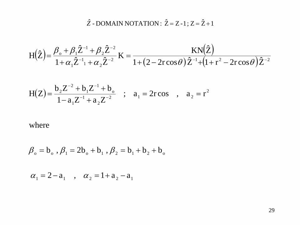
1ZZ;1-ZZ :NOTATION DOMAIN - ˆ +==Z
( ) ( )( ) ( )
( )
12211
o2121o1oo
2212
21
1
o1
12
2
221221
11
22
11o
aa1,a2
bbb,bb2,b
where
ra,cosr2a;ZaZa1
bZbZbZH
Zcosr2r1Zcosr221ZKNK
ZZ1ZZZH
−+=−=
++=+==
==+−
++=
−++−+=
++++
=
−−
−−
−−−−
−−
αα
βββ
θθααβββ
29

LP 20 (bilinear transform)
LP 11
LP 10
LP 02 (forward transform)
LP 01
LP 00 (backward transform)
BP 10 ((bilinear transform)
BP 01 (forward)
BP 00 (backward)
HP
( )21 4ˆ41 −− ++ zzK
( ) 11 ˆ1ˆ2 −− + zzK
( )1ˆ3ˆ3ˆ2 112 ++ −−− zzzK
( ) 11 ˆˆ1 −−+ zzK
( )21ˆ1 −+ zK
2−Kz
( )1ˆ21 −+ zK
1ˆ −zK( )1ˆ1 −+ zK
K
LPN
( )211 −+ zK
( )11 1 −− + zKz
( )11 −+ zK
K
2−Kz1−Kz
( )( )11 11 −− +− zzK
( )11 1 −− − zKz
( )11 −− zK( )211 −− zK( ) 0,,1 21 >>++ −− ββαεε zzK ( ) ( )[ ]21 ˆ22ˆ1 −− ++++ zzK εε
HPN ( ) 0,,1 21 ><++ −− ββαεε zzK ( ) [ ][ ]21 ˆ22ˆ1 −− ++++ zzK εε
AP ( )21 −− ++ zzK αβ See Eq. (21), Sect. 5.1 21 , αβαα =−=
Generic Biquadratic Transfer Functions in the 2r and cosr2 domain, z ==− βθα
GENERIC FORM NUMERATOR N(z) NUMERATOR N( ) z
30

Recall notation for and building blocks Z Z
- +
- +
φ1 φ1 KiC Vin
φ2 φ2
C
φ1 Vo Vin
-Ki 1ˆ1 −+ Z Vo
Vin φ1 KnC
φ2 φ1
φ2
C
φ1 Vo Vin
Kn 1ˆ −Z Vo
Vin -Ki
111
−− ZVo
Vin -Ki
1
1
1 −
−
− ZZ
Vo
31

2V
oinV ∑
∑
∑
∑
o
o
1V
)1z( 1 +− I−
1z− F− )z1( 1−+
J
A
H1z− E−
)z1( 1−+
C−G−
A general SC biquad flow diagram type 1. 32

SC implementation type 1 with maximum number of switches.
2φ
A1φ
• • +
−1φ
2φ2φ
o2V
2φ F
1φ1φ
2φ
B
2φ I
1φ 1φ
2φ
2φ
J1φ
1φ
2φ
o
1V
• +
−
D
2φ C
1φ1φ
2φ
E
2φ G
1φ1φ
2φ
2φ
H1φ
1φ
2φ
o
inV+
− o
33

SC implementation type 1 minimum switch configuration.
2φ
A1φ
• • +
−1φ
2φo
2V
B
I
J
1φ
2φ
o
1V
• +
−
D
C
2φ G
1φ1φ
2φ
2φ
H1φ
o
inVo
6
•9
•5
•
•7
•834
E
F
•
•2•120
34

SWITCAP Input file
timing; period 7.8125e-06; clock clk 1 (0 1/2); end; circuit; cg (1 2) 2.5935; ca (8 7) 1.0000; cd (4 3) 29.9613; cb (6 5) 12.0365; ce (4 5) 1.00000; cc (2 9) 2.5035; e1 (3 0 0 4) 28000; e2 (5 0 0 6) 28000; s1 (20 1) #clk;
s4 (2 4) #clk; s5 (9 5) #clk; s9 (8 0) #clk; s10 (7 6) #clk; s2 (1 0) clk; s3 (2 0) clk; s6 (9 0) clk; s7 (3 8) clk; s8 (7 0) clk; v1 (20 0); end; analyze sss; infreq 1 4000 lin 300; set v1 ac 1.0 0.0; print vm(5); plot vm(5);
35

36

• Switched-capacitor techniques conventionally have only two degrees of freedom: clock frequency
capacitor ratios
i.e.,
eqseq
seq C
CfC
CTCR ⋅=⋅
==1τ
-37-
Francisco Duque-Carrillo & Edgar Sánchez-Sinencio
37

Periodic Non-Uniform Switched Capacitor Principle
• The number of active pulses (pi) of a switched-capacitor branch controls the equivalent resistance value.
Vo
Master CLK
φi
sTm ⋅
si
Tp ⋅
⋅⋅=⋅=
1CCT
pmCR s
ieqτ
1 2 pi
sT
-38-
viφ1 φ1
φ2 φ2
C1
C
vo
+
−
An additional degree of freedom (m/pi) is provided by this approach
38

Periodic Non-Uniform Switched-Capacitor Example
• In more complex switched-capacitor networks, any response parameter can be fully-programmed by means of the number of active pulses of some switched-capacitor branches:
DC gain:
2
1)0(CC
ppH
f
k ⋅=
Cutoff frequency (ωo): f
sop
CCCmTjez
+
==2
ω
-39-
C
vivo
C1
C2
φ1k φ2k
φ1kφ2k
φ2f φ2f
φ1f φ1f
φ1f
mTS
φf 1 2 3 pf
φk 1 2 pk
fs
39

Periodic Non-Uniform Switched-Capacitor Remarks Advantages: • Great flexibility and resolution for programming SC signal processors. • The design is performed in the digital domain with a single logic programmable section (i.e., FPGA). • Reduced cost (area) and high accuracy (no extra parasitic capacitances) respect to any other programming technique (i.e., capacitor arrays). • Only one clock is used. One sub-clock (φi) is required for each output response parameter to be programmed. • The programmability does not affect the circuit dynamic range.
Disadvantages: • The master clock frequency must be m times the clock frequency of the traditional case (pi=m). However, the amplifier requirements remain unchanged. -40-
40

-41-
HP HP
A
B
-
+
-
+
φ 1f LP φ
1f
G
C φ
1f
I
F
A1 A2 V o
E
φ 1f
D
φ 1f
φ 1f
φ 1f K
BP
V i φ
2f φ
2f
φ 2f
φ 2f
φ 2f
φ 2f
φ 2f
φ 2f
φ 2q
φ 1q
φ 2q
φ 1q
φ 2f
Example of the Proposed Technique
•Universal second-order SC filter (CMOS 1.2 µm, Vsupply= + 1.5 V)
Design specifications { fo = 0.2 kHz, Q = 0.707, k = 0 dB } with fs = 20 kHz
The SC circuit was designed to operate with clock frequencies up to 1 MHz
The digital programming signals were off-chip generated by a commercial FPGA 41

Experimental Results of Second-Order Non-Uniform SC 1. Low-pass response programmability (m = 8, fs = 160 kHz)
Swp Time: 19.66 SecVBW: OffRange 0 dBmRes BW: 9.1 HzA: NORMALIZED SPEC
Stop 800 HzStart 50 Hz
LogMag 5dB /div
-25
25dB
LP fo-programmability (1 < pf < 8)
LP Q-factor programmability (1 < pq < 8)
Swp Time: 31.13 SecVBW: OffRange 0 dBmRes BW: 18 HzA: NORMALIZED SPEC
Stop 5 000 HzStart 50 Hz
LogMag 3dB /div
-28
2dB
-42- 42

Experimental Results (continues) 2. fo Band-pass response programmability
Swp Time: 31.13 SecVBW: OffRange 0 dBmRes BW: 36 HzA: NORMALIZED SPEC
Stop 20 000 HzStart 100 Hz
LogMag 4dB /div
-36
4dB
m = 8; fs = 160 kHz (1 < pf < 8)
m = 24; fs = 960 kHz (1 < pf < 24)
Swp Time: 13.11 SecVBW: OffRange 0 dBmRes BW: 36 HzA: NORMALIZED SPEC
Stop 4 000 HzStart 50 Hz
LogMag 2dB /div
-18
2dB
-43-
Note the increased resolution
43

Experimental Results (continues) 3. Q-factor band-pass programmability
m = 8; fs = 160 kHz (1 < pq < 8)
m = 32; pf = 3; fs = 1 MHz (1 < pq < 25)
Swp Time: 31.13 SecVBW: OffRange 0 dBmRes BW: 18 HzA: NORMALIZED SPEC
Stop 5 000 HzStart 200 Hz
LogMag 6dB /div
-20
40dB
Swp Time: 13.11 SecVBW: OffRange 0 dBmRes BW: 36 HzA: NORMALIZED SPEC
Stop 800 HzStart 50 Hz
LogMag 5dB /div
-20
30dB
-44-
Enhanced Resolution
44
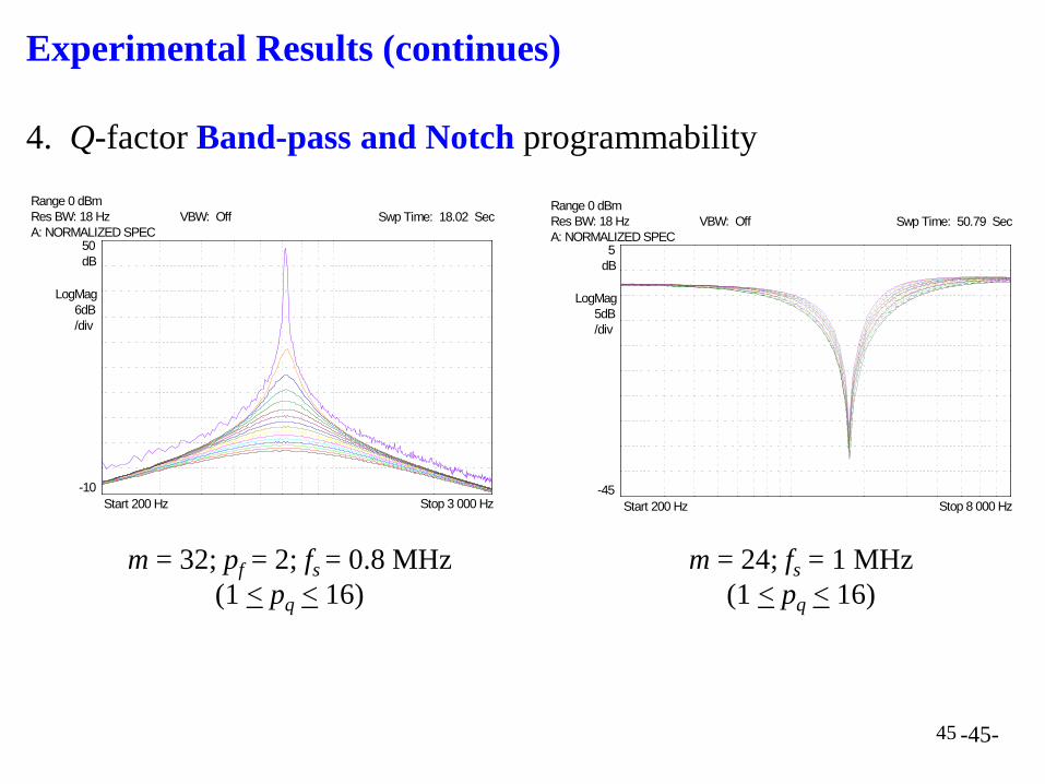
Experimental Results (continues) 4. Q-factor Band-pass and Notch programmability
m = 32; pf = 2; fs = 0.8 MHz (1 < pq < 16)
m = 24; fs = 1 MHz (1 < pq < 16)
Swp Time: 50.79 SecVBW: OffRange 0 dBmRes BW: 18 HzA: NORMALIZED SPEC
Stop 8 000 HzStart 200 Hz
LogMag 5dB /div
-45
5dB
Swp Time: 18.02 SecVBW: OffRange 0 dBmRes BW: 18 HzA: NORMALIZED SPEC
Stop 3 000 HzStart 200 Hz
LogMag 6dB /div
-10
50dB
-45- 45

Conclusions
A SC technique with an additional degree of freedom is presented. Potential applications are very wide and practical implications are very promising. The ideal situation of analog processing and digital control are present in the proposed scheme.
46
outVinV −
+ • 1C
Bφ• •
Aφ
•
1φ
• •
2φ
•
•
1φ
2φ
3C
2C
)()()()(
21
12
cacaB
cacaA
φφφφφ
φφφφφ
•+•=
•+•=
(a)
•
• •
•
Bφ
Aφ
1φ
2φ
caφ
(b)
(a) A switched-capacitor square-wave modulator where the input clock phases are controlled by the modulating square wave φM. (b) A possible circuit realization for φA and φB.
A full-wave detector based on the square-modulator circuit of Fig. (a)
(a) Fig.ofModulator
+−
caφ
inV outV
47

High-Q bandpass filter with center frequency f0
Period T
Period T = 1/f0
A BP Filter based sinusoidal oscillator.
1VrefV
outV
refV−
sin (wot)
48

−
+outV
• •
•
4C
• 1φ
2φ
refV+−+
• 2φ
• •
•
1φ X
•
1φ X
2φ
1φ
1φ
•
2φ
•
1=BC
1=AC
•
2C
• 1φ2φ
1φ
1C
5C
2φ
+−
+−
6C
3C
Comp
7CstVStart-up
circuit • X
X
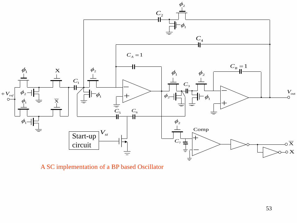
A SC implementation of a BP based Oscillator
49

References • E. Sanchez-Sinencio, J. Silva-Martinez, The Circuits and Filters Handbook: Switched Capacitor Filters, CRC Press Inc., section XV, pp. 2491-2520, 1995. • E. Sanchez-Sinencio, R.L. Geiger and J. Silva-Martinez, “Tradeoffs between Passive Sensitivity, Output Voltage Swing and Total Capacitance in Biquadratic SC Filters,” IEEE Trans. Circuits and Systems, Vol. CAS-31, No. 11, pp. 984-987, November 1984. • E. Sanchez-Sinencio, J. Silva-Martinez, and R.L. Geiger, “Biquadratic SC Filters with Small GB Effects,” IEEE Trans. Circuits and Systems, Vol. CAS-31, No. 10, pp.876- 884, October 1984. • R. Castello, F. Montecchi, F. Rezzi and A. Baschirotto, “Low-Voltage Analog Filters,” IEEE Trans. on Circuits and Systems I, Vol. 42, No. 11, pp. 827-840, November 1995. • A. Abo, “Low Voltage, High-Speed, High-Precision Switched-capacitor Circuits,” Qualifying Exam, University Of California at Berkeley, May 1996.
50

outVinV −
+ • 1C
Bφ• •
Aφ
•
1φ
• •
2φ
•
•
1φ
2φ
3C
2C
)()()()(
21
12
cacaB
cacaA
φφφφφ
φφφφφ
•+•=
•+•=
(a)
•
• •
•
Bφ
Aφ
1φ
2φ
caφ
(b)
(a) A switched-capacitor square-wave modulator where the input clock phases are controlled by the modulating square wave φM. (b) A possible circuit realization for φA and φB.
A full-wave detector based on the square-modulator circuit of Fig. (a)
(a) Fig.ofModulator
+−
caφ
inV outV
51

High-Q bandpass filter with center frequency f0
Period T
Period T = 1/f0
A BP Filter based sinusoidal oscillator.
1VrefV
outV
refV−
sin (wot)
52
−
+outV
• •
•
4C
• 1φ
2φ
refV+−+
• 2φ
• •
•
1φ X
•
1φ X
2φ
1φ
1φ
•
2φ
•
1=BC
1=AC
•
2C
• 1φ2φ
1φ
1C
5C
2φ
+−
+−
6C
3C
Comp
7CstVStart-up
circuit • X
X
A SC implementation of a BP based Oscillator
53

References • E. Sanchez-Sinencio, J. Silva-Martinez, The Circuits and Filters Handbook: Switched Capacitor Filters, CRC Press Inc., section XV, pp. 2491-2520, 1995. • E. Sanchez-Sinencio, R.L. Geiger and J. Silva-Martinez, “Tradeoffs between Passive Sensitivity, Output Voltage Swing and Total Capacitance in Biquadratic SC Filters,” IEEE Trans. Circuits and Systems, Vol. CAS-31, No. 11, pp. 984-987, November 1984. • E. Sanchez-Sinencio, J. Silva-Martinez, and R.L. Geiger, “Biquadratic SC Filters with Small GB Effects,” IEEE Trans. Circuits and Systems, Vol. CAS-31, No. 10, pp.876- 884, October 1984. • R. Castello, F. Montecchi, F. Rezzi and A. Baschirotto, “Low-Voltage Analog Filters,” IEEE Trans. on Circuits and Systems I, Vol. 42, No. 11, pp. 827-840, November 1995. • A. Abo, “Low Voltage, High-Speed, High-Precision Switched-capacitor Circuits,” Qualifying Exam, University Of California at Berkeley, May 1996.
54

J. L. Ausin, J. F. Duque-Carillo, G. Torelli, E. Sánchez-Sinencio, and F. Maloberti, “Periodical nonuniform individually sampled switched-capacitor circuits,” ISCAS 2000, pp. 449-452, May 2000, Geneva, Switzerland P. E. Fleischer and K.R. Laker, “A family of active switched-capacitor biquad building blocks,” Bell Syst. Tech J., vol. 58, pp. 2253-2269, Oct. 1979. J. Adut and J. Silva-Martínez, “A high-Q switched-capacitor filter with reduced capacitance spread using a randomized noninterval sampling technique”, ISCAS 2002 submitted.
55