Embed Size (px)
Citation preview

A design of selective solar absorber for high temperature applications
A. AL-Rjouba,1, L. Reboutaa, P. Costaa, N.P. Barradasb, E. Alvesc, P.J. Ferreirad, e, K. Abderrafid, A. Matilainenf, K. Pischowf a Centre of Physics, University of Minho, Campus de Azurém, 4800-058 Guimarães, Portugal b Centro de Ciências e Tecnologias Nucleares, Instituto Superior Técnico, EN 10, km 139.7, 2695-066 Bobadela LRS, Portugal c Campus Tecnológico e Nuclear, Instituto Superior Técnico, EN 10, km 139.7, 2695-066 Bobadela LRS, Portugal d International Iberian Nanotechnology Laboratory, Av. Mestre José Veiga s/n, 4715-330 Braga, Portugal e Materials Science and Engineering Program, The University of Texas at Austin, Austin, USA f Savo Solar Oy, Insinöörinkatu 7, 50100 Mikkeli, Finland
Abstract
This study presents a design of multilayer solar selective absorber for high temperature applications.
The optical stack of this absorber is composed of four layers deposited by magnetron sputtering on
stainless steel substrates. The first is a back-reflector tungsten layer, which is followed by two
absorption layers based on CrAlSiNx/ CrAlSiOyNx structure for phase interference. The final layer is an
antireflection layer of SiAlOx. The design was theoretically modelled with SCOUT software using
transmittance and reflectance curves of individual thin layers, which were deposited on glass substrates.
The final design shows simultaneously high solar absorbance α= 95.2 % and low emissivity ε= 9.8%
(at 400 ºC) together with high thermal stability at 400 ºC, in air, and 600 ºC in vacuum for 650 h.
Keywords: solar selective absorber, optical constants, dielectric function, sputtered CrAlSiNx
/CrAlSiOyNx
1. Introduction
Solar thermal energy is already being used for electricity production by using the concentration solar
power (CSP) technology. This technology uses parabolic-trough solar systems that concentrate sunlight
up to 80 times onto evacuated receiver tubes. The energy is absorbed at the solar absorption pipe by the
coated selective layers. The resulting energy can be subsequently used in steam turbines to produce
electricity (Fernández-García et al., 2010)(Odeh et al., 1998)(Ward, 1997). However, comparing with
other resources, the relative cost of electricity generated by solar thermal technology is still high. The
cost can be reduced by improving the optical and thermal properties of the coating materials, and by
increasing the operating temperature more than 450 ºC (Rebouta et al., 2015) and by improvements in
the long-term stability. These improvements can be done by an adequate materials selection (Kennedy,
1 Corresponding author – e-mail address: [email protected] (A. AL-Rjoub)

2002), maintaining the optical performance at higher temperatures and with higher durability. Efficient
designs should have high absorbance (α) at solar radiation region (wavelength range of 0.3- 2.0 µm),
low thermal emittance in IR region (wavelength range greater 2.0 µm) and long-term resistance against
oxidation and barrier diffusion at high temperature.
Most of selective solar absorber coatings are based on metal-dielectric nanocomposite coatings
(Cermet), such as Mo-Al2O3 (Zhang et al., 2006), Pt-Al2O3 (Nuru et al., 2012), WTi-Al2O3(Wang et al.,
2017) and AlSiOx:W (Dias et al., 2017). With these kinds of material, it is easy to tune the optical
properties and the optical constants of the different layers, which can be done by varying the metal
volume factor of ceramic layers. As a result, it is possible to optimize the absorptance according to the
double interference theory of absorption (Zhang et al., 1992). Moreover, all those absorbers are
multilayers coating that consist of IR-reflective metallic base layer such as tungsten or molybdenum, a
double interference absorption (high absorber (HA) and low absorber (LA)) layers and a ceramic anti-
reflection (AR) surface layer (Rebouta et al., 2015). However, such coatings have limited durability at
higher temperature due to oxidation or diffusion of the metal component in the dielectric matrix, which
limits their applications (Selvakumar and Barshilia, 2012).
Other designs are based on layers of metal nitrides and oxynitrides structure, such as
TiAlN/TiAlON/Si3N4 (Barshilia et al., 2007), W/AlSiN/AlSiON/AlSiOy (Rebouta et al., 2015), and
AlCrSiN/AlCrSiON/AlCrO (Zou et al., 2016). Those stacks show high oxidation resistance and high
thermal stability at high temperatures, because of nitrides and oxynitrides, which show good
mechanical, chemical and thermal properties at higher temperature.
This work presents a new design of solar selective absorber for high temperature applications, based
on nitrides and oxynitrides with structure (W/CrAlSiNx /CrAlSiOyNx/SiAlOx).
2. Experimental
All layers were deposited by dc magnetron sputtering (PAr=0.37 Pa, current density 6.4 mA/cm2,
pulsed bias of -60 V, f =90 kHz, room temperature and base pressure 2×10⁻⁴ Pa), except in tungsten layer
case, where the current density was 12.7 mA/cm2. The stainless steel substrates were ultra sound cleaned
in acetone for 15 min, and ion etched prior the deposition. Individual layers of CrAlSiNx and CrAlSiOyNx
were deposited on glass substrates with different nitrogen and oxygen partial pressures for 1 min.
Spectrophotometry measurements (Shimadzu PC3100 spectrophotometer), in the wavelength range of
0.25 – 2.5 µm, were used to measure the transmittance and the reflectance of those layers, and the
reflectance data was corrected according to the Al -reference reflectance curve. Those results were used to
calculate the optical constants and thicknesses of designed layers by using SCOUT software (Theiss,
2002). With the data obtained from individual layers, the selective absorber stack was designed, and it

was deposited on stainless steel substrates. Then, it was annealed in air and vacuum at 400 ºC and 600 ºC,
respectively.
The normal solar absorptance (αs) was determined from equation (1) by calculated or experimental
spectral reflectance data R(λ) and ASTM AM1.5D solar spectral irradiance, Is(λ), at the wave range of 0.3
– 2.5 µm (Bogaerts and Lampert, 1983).
..
..
(1)
On the other hand, A Fourier Transform Infrared (FTIR) spectrophotometer from Agilent
Technologies equipped with a gold integrating sphere and a HgCdTe (MCT) detector was used
to measure the spectral reflectance in the infrared wavelength range, 1.6-16.7 µm. The normal
thermal emittance was calculated as the weighted fraction between emitted radiation and the
Planck black body distribution at a specific temperature T, using the spectral blackbody emissive
power and the spectral reflectance.
For structural and oxidation resistance studies, glancing incident angle XRD was used for samples
before and after annealing, that was performed by employing a Bruker AXS Discover D8 operating with
Cu Kα radiation. The measurements were performed at fixed incidence angle of α = 3º. Scanning electron
microscopy (SEM) was performed with a Nano SEM–FEI Nova 200(FEG/SEM) microscope. Energy
dispersive X-ray Spectroscopy (EDS) analyzes were performed with the electron beam of the SEM, with
an energy of 13.5 keV (EDAX - Pegasus X4M system).
The comparison of chemical composition of stack (as deposited, after air and vacuum annealing) was
done by using Rutherford Backscattering (RBS) measurements, which were done at the CTN/IST Van de
Graaff accelerator using 2 MeV 4He+ and 2.3 MeV 1H+ beams and detectors at 140º and 165º to the beam
direction. Normal incidence was used in the experiments and the obtained data were analysed with the
IBA Data Furnace NDF (Barradas and Jeynes, 2008).
3. Results and discussion
3.1 Optical properties of single layers
CrAlSiNx / CrAlSiOyNx thin layers were previously studied and their optical properties were reported
(Al-Rjoub et al., 2017), a series of individual thin layers based on CrAlSiNx /CrAlSiOyNx were deposited
with different nitrogen and oxygen partial pressures as reactive gases. Fig. 1 shows the optical constants,
refractive index (n) and extinction coefficient (k), as a function of wavelength in the range of 250 – 2500
nm, which were obtained from modeling of the experimental T and R spectra. It shows the general

behavior of n and k with a decrease as the gases partial pressures increase for both nitride and oxynitride
layers. Moreover, it is seen that the refractive indices for the CrAlSiNx layers increase in the wavelength
range of 300 – 1000 nm, which make these layers appropriate materials for selective absorption of solar
radiation and other optical applications, because it contributes to the solar absorption enhancing through
the interference effect. Refractive indices and thicknesses of the bilayer structure should be chosen in
order to obtain destructive interference at wavelengths around 0.5 µm and 1.3 µm, contributing to the
decrease of the reflectance of the solar radiation and consequently improving its absorptance. An optical
path length (product of the refractive index with the thickness, nd) of 1/4 wavelength (in a layer) would
produce a net shift of 1/2 wavelength between the light reflected from the top surface and from the bottom
interface, resulting in cancellation (Yin and Collins, 1995). The increase of refractive index in the
wavelength range of 300 – 1000 nm allows to have a broad range with high degree of destructive
interference effect.
The refractive index of CrAlSiOyNx layers also shows a similar behavior with wavelength, but for high
gases partial pressures it becomes almost constant.
Fig. 1: Refractive index (n) and extinction coefficient (k) as a function of wavelength of: (a) CrAlSiNx, prepared with increasing nitrogen partial pressure. (b) CrAlSiOyNx as a function of wavelength, prepared with increasing nitrogen and oxygen partial pressures.
Elemental Tungsten is a good candidate for back-reflector layer in selective thermal absorber tandem,
due to its high temperature melting point and due to high reflectance in IR region of radiation (R% = 94.6
500 1000 1500 2000 25000.0
0.5
1.0
1.5
2.0
2.5
3.0
3.5
0.0
0.5
1.0
1.5
2.0
2.5
3.0
3.5 CrAlSiNx
R
efra
ctiv
e in
dex
(n)
Ext
inct
ion
inde
x (k
)
(a)
0.037 0.051 0.056 0.060 0.071
Wavelength λ (nm)
500 1000 1500 2000 25000.0
0.5
1.0
1.5
2.0
2.5
3.0
3.5
0.0
0.5
1.0
1.5
2.0
2.5
3.0
3.5 0.046 0.064 0.068 0.075 0.092
CrAlSiOyNx
(b)
Wavelength λ (nm)
Ref
ract
ive
inde
x (n
)
Ext
inct
ion
inde
x (k
)

at λ > 2.5 µm) as shown in Fig. 2. High reflectivity of W in IR region decreases the emissivity of stacks.
In addition, W also contributes in energy absorption at solar radiation region, due to its reflectance in
visible region (Fig. 2). More information about optical constants (n and қ) as a function of wavelength (λ)
is shown in Fig. 2.
Fig. 2: Reflectance, n and қ of tungsten deposited on polished stainless steel.
Finally, the antireflection layer (SiAlOx) has a very low extinction coefficient (almost goes to zero)
and it has a refractive index around 1.50, as shown in Fig. 3. In accordance to that, this layer is
transparent and it is a good candidate for antireflective layer. Moreover, it protects other layers against
oxidation.
Fig.3: Refractive index (n) and extinction coefficient (қ) of the antireflection layer (SiAlOP= 0.062 Pa)
3.2 The structure of single layers
XRD was performed for single layers used in the absorber stack. As shown in Fig. 4, all layers are
amorphous except W layer. Despite the W coatings showed a combination of both α- and β- phase of
growth, the α- phase is the dominant. So, W is polycrystalline with (110) orientation (2θ= 40º) (Sibin et
500 1000 1500 2000 250020
40
60
80
100
n, κ
R% n k
Wavelength (λ) nm
Ref
lect
ance
(R%
)
2
4
6
8
10
12
14
500 1000 1500 2000 25001.2
1.3
1.4
1.5
1.6
1.7
Ext
inct
ion
coef
ficie
nt (k
)
Ref
ract
ive
inde
x (n
)
Wavelength λ(nm)
0.0
0.1
0.2
0.3
0.4
0.5

al., 2015)(Shen and Mai, 2006). Indeed, SEM cross sectional micrographs of thick single layers are
completely agreeing with the XRD analysis, as shown in Fig. 5.
Fig. 4: XRD patterns of single layers performed with fixed incidence angle of 3º of: W deposited on stainless steel, CrAlSiN P=0.051 Pa, CrAlSi(ON) P=0.068 Pa and SiAlO P= 0.062 Pa layers deposited on silicon substrate.
Fig. 5: Cross-sectional SEM micrographs of (a) CrAlSiNP= 0.051 Pa, (b) CrAlSiONP= 0.068 Pa, (c) SiAlOP=0.062 Pa and (d)
Tungsten (W) as thick single layers.
30 40 50 60 70
SiAlOP=0.062 Pa
CrAlSi(ON)P=0.068 Pa
CrAlSiNP=0.051 Pa
W
β −W
(320
)
α−W
(200
)
β −W
(200
)
α−W
(110
)
Inte
nsity
[a.u
]
2θ (Degree)

3.3 Design of the multilayer
The design was theoretically modelled with SCOUT software using transmittance and reflectance
curves of individual thin layers that were deposited on glass substrates. SCOUT allows the calculation of
the spectral optical constants, refractive index (n) and extinction coefficient (қ), besides the thickness of
each individual layer. The used model enables to evaluate the complex dielectric function ( )
as frequency dependence, which is a result of a combination of several different types of oscillators, each
with their own characteristic resonant frequency. So, the dielectric function is considered as a sum of
several contributions that describe the intraband and interband transitions, as shown in equation (2)
∑ (2)
where , , and are background, Drude model for susceptibility of free
carriers, harmonic oscillators for vibrational modes and OJL model for interband transitions, respectively
(Bogaerts and Lampert, 1983)(Learys et al., 1998). Then, the complex refractive index ( ) can be
calculated from the relation , where n is the refractive index and қ is the extinction
coefficient. Efficient selective absorber can be achieved, if it has a graded refractive index and extinction
coefficient that decrease from back-reflector W-layer towards the antireflection layer. In ideal case, at the
front of the antireflection layer, n and қ should be 1 and 0, respectively. (Craighead et al., 1979) (Farooq
and Lee, 2003).
Beginning with individual thin layers deposited on glass, the final tandem is obtained with a layer`s
structure, thicknesses and simulated reflectance curve, as shown in Fig. 6.
Fig. 6: (a) Schematic diagram of the simulated multilayer as obtained by SCOUT. (b) Simulated and experimental reflectance curves of the absorber design.
500 1000 1500 2000 25000
20
40
60
80
α = 95.5 % As simulated α = 95.0 % As deposited
(b)
Ref
lect
ance
( R
%)
Wavelength λ (nm)

As shown in Fig. 6a, the optical stack is composed of four layers, the first is a back-reflector tungsten
layer, which is followed by two absorption layers based on CrAlSiNx / CrAlSiOyNx structure for phase
interference. The final layer is an antireflection layer, that consists of SiAlOx. The total simulated
thickness of the whole multilayers absorber (W/CrAlSiNx /CrAlSiOyNx /SiAlOx) is ~ 316 nm. The
experimental design shows good agreement with simulated one except small differences in the reflectance
curves and absorption value, as shown in Fig. 6b. This is due to the parameters of reactive sputtering
deposition, where small variations can happen. The final design shows simultaneously high solar
absorbance in average α= 95.2 % and low emissivity ε= 9.8 % (at 400 ºC).
In accordance to that, Fig. 7 shows a cross-sectional SEM micrograph of the optical stack, deposited
on silicon substrate. W layer shows a typical morphology of a columnar growth type, whereas the
remaining layers reveal a featureless morphology that completely agrees with XRD analysis.
Fig. 7: Cross-sectional SEM micrograph of the optical stack, deposited on silicon substrate.
3.4 Thermal stability
For long lifetime, selective absorber stack should have good resistance of oxidation and it should be
thermally stable. So, the optical stack was subjected to annealing tests in air at 400 ºC and in vacuum at
600 ºC for 650 h. Then, the absorbance (α) was measured after each annealing step, and the emittance
(ε) was calculated for each sample as deposited and for the last step of thermal annealing. Fig. 8a
represents the reflectance curves of as deposited, after 350h and after 650h of air annealing. There is a
very small shift in the step of the reflectance curve towards lower wavelength. As a result, the solar
absorptance was improved a bit and the absorber stack shows good thermal stability. Fig. 8b shows the

reflectance curves of as deposited, and vacuum annealed samples for 50h, 350h and 650h. Now, the
shift towards lower wavelength was higher than air annealing case, especially after the first step of
annealing (50 h). After further steps of vacuum annealing the changes were small, this demonstrates
that the optical stack has very good thermal stability at this temperature. The shift caused a small
decrease in solar absorptance (from 95.4 % to 95.0 % as shown in Figure 8b), but the emissivity
improved (it decreased from 11.4% to 9.4% at 400 ºC). The change after first step can be related with
oxidation of some Si atoms not yet completely oxidized and with desorption of some water vapor
incorporated during deposition. Changes in additional steps can also be related with the diffusion of
layer elements (such as the diffusion of Cr towards surface as will see in RBS analysis).
Fig. 8: Reflectance of as deposited optical stack and after (a) air thermal annealing at 400 ºC (b) vacuum thermal annealing at 600 ºC, with measured value of thermal absorptance (α) and thermal emittance (ε) (calculated for 400 ºC). Elemental depth profiles of the absorber were studied by Rutherford back scattering (RBS). Fig. 9
shows RBS spectra of three optical stacks deposited in same run and subjected to different thermal load,
namely as deposited, after air annealing at 400 ºC for 650 h and after vacuum annealing at 600 ºC for 650
h. Since the signals from the different elements can overlap, the composition should be determined from
the front edges of the elements, which are indicated in the figure. The relative heights of those front edges
are correlated with the relative concentrations of the different elements. The position of the different
elements, if located at surface sample, are indicated in the graph. It is difficult to distinguish between
silicon and aluminum because of the small difference of their atomic mass. However, the analysis shows a
small difference between as deposited and annealed samples. After air annealing a small change is seen in
the stainless steel substrate, which was not clearly identified. After vacuum annealing at 600 ºC, it can be
seen changes of W and Cr depth profiles, which are in accordance with the diffusion of small amount of
tungsten towards the stainless steel substrate and chromium, mainly from CrAlSiOyNx layer, towards the
1000 100000
20
40
60
80
100 As Deposited α = 95.0 %, ε = 9.8% 350h, α = 95.1 % 650h, α = 95.1 %, ε = 9.7%
(a)
400 oC in Air
Ref
lect
ance
( R
% )
Wavelength λ ( nm )1000 10000
0
20
40
60
80
100 As Deposited α = 95.5 %, ε = 11.4% 50h, α = 95.4 % 350h, α = 95.3 % 650h, α = 95.0 %, ε = 9.4%
600 oC in Vacuum
(b)R
efle
ctan
ce (
R%
)
Wavelength λ ( nm )
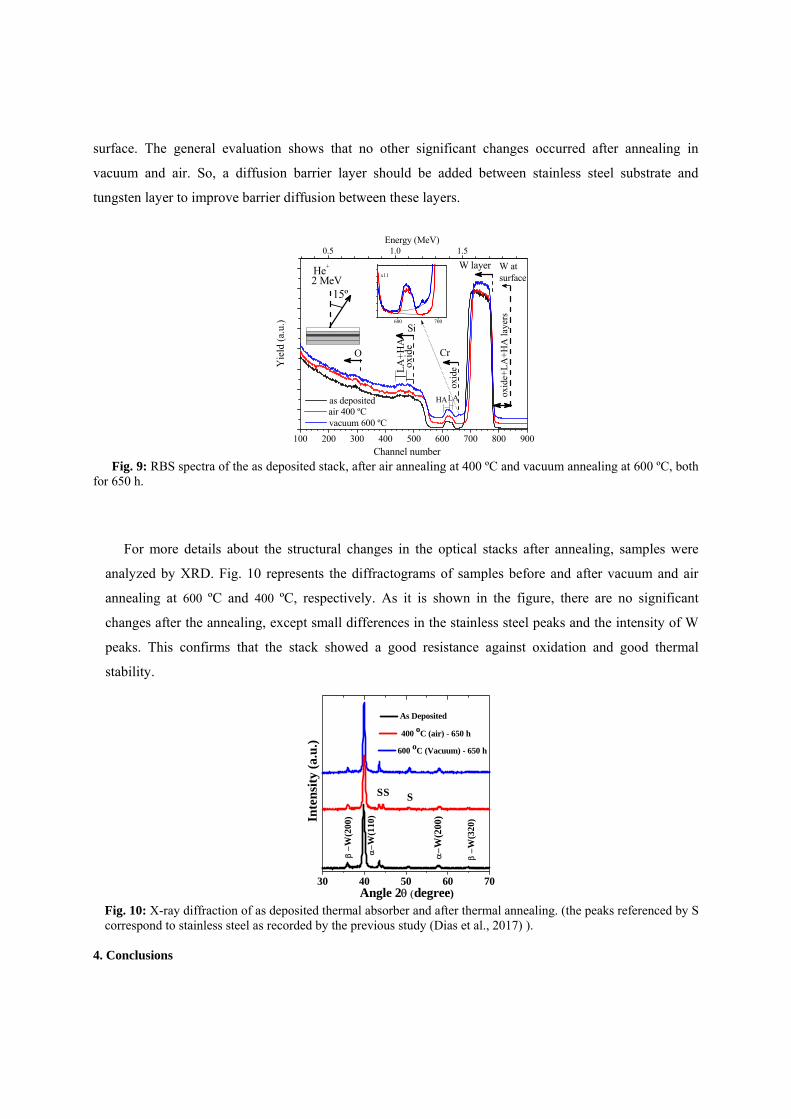
surface. The general evaluation shows that no other significant changes occurred after annealing in
vacuum and air. So, a diffusion barrier layer should be added between stainless steel substrate and
tungsten layer to improve barrier diffusion between these layers.
Fig. 9: RBS spectra of the as deposited stack, after air annealing at 400 ºC and vacuum annealing at 600 ºC, both
for 650 h.
For more details about the structural changes in the optical stacks after annealing, samples were
analyzed by XRD. Fig. 10 represents the diffractograms of samples before and after vacuum and air
annealing at 600 ºC and 400 ºC, respectively. As it is shown in the figure, there are no significant
changes after the annealing, except small differences in the stainless steel peaks and the intensity of W
peaks. This confirms that the stack showed a good resistance against oxidation and good thermal
stability.
Fig. 10: X-ray diffraction of as deposited thermal absorber and after thermal annealing. (the peaks referenced by S correspond to stainless steel as recorded by the previous study (Dias et al., 2017) ).
4. Conclusions
100 200 300 400 500 600 700 800 900
600 700
x11
oxid
e
O
LA+H
Aox
ide
Yie
ld (a
.u.)
Channel number
as deposited
oxid
e+LA
+HA
laye
rs
W atsurface2 MeV
He+
15º
W layer
Cr
Si
air 400 ºCHA
vacuum 600 ºC
LA
0.5 1.0 1.5 Energy (MeV)
30 40 50 60 70
β −W
(320
)
α−W
(200
)
α−W
(110
)
β −W
(200
)
As Deposited
Inte
nsity
(a.u
.)
Angle 2θ (degree)
600 oC (Vacuum) - 650 h
S SS
400 oC (air) - 650 h

A design of selective solar absorbance for high temperature applications was fabricated by magnetron
spattering method. It is a multilayer that consists in a structure of four layers (W/CrAlSiNx
/CrAlSiOyNx /SiAlOx), as back reflector/ high absorber/ low absorber/antireflector layers, respectively.
The total thickness of the stack is ~ 327 nm as measured by SEM. The structure was simulated by the
SCOUT software. Experimental design shows simultaneously high average solar absorbance α=95.2%
and low emissivity ε= 9.8% (at 400 ºC) together with high thermal stability at 400 ºC, in air and at 600
ºC, in vacuum, for 650 h. After the first step of thermal annealing in vacuum at 600 ºC, the reflectance
curve of the stack shifted towards lower wavelength, which caused a decrement in the value of solar
absorbance. However, after further steps of annealing, no significant changes were seen. In most
cases, thermal emissivity improved a bit or stayed constant, which implies that the W back reflector
layer maintained its reflectivity meaning it is well protected by the outermost layers. On other hand, it
was recorded by RBS analysis that a small amount of W diffused toward stainless steel substrate. This
diffusion can be easily controlled by adding a diffusion barrier layer between stainless steel substrate
and tungsten layer. Finally, the CrAlSiNx /CrAlSiOyNx and SiAlOx layers show a featureless
morphology, which is in accordance with the XRD amorphous like structure. The W layer showed a
combination of both α- and β- phase of growth, but the α- phase is dominant and it is polycrystalline
with (110) orientation.
ACKNOWLEDGMENTS The authors acknowledge the support of FCT in the framework of the Strategic Funding UID/FIS/04650/2013 and the financial support of FCT, POCI and PORL operational programs through the project POCI-01-0145-FEDER-016907 (PTDC/CTM-ENE/2882/2014), co-financed by European community fund FEDER.
References Al-Rjoub, A., Costa, P., Rebouta, L., Cerqueira, M.F., Alpuim, P., Barradas, N.P., Alves, E.,
2017. Characterization of magnetron sputtered sub-stoichiometric CrAlSiNx and CrAlSiOyNx coatings. Surf. Coat. Technol. doi:10.1016/j.surfcoat.2017.08.038
Barradas, N.P., Jeynes, C., 2008. Advanced physics and algorithms in the IBA DataFurnace. Nucl. Instruments Methods Phys. Res. Sect. B Beam Interact. with Mater. Atoms 266, 1875–1879. doi:10.1016/j.nimb.2007.10.044
Barshilia, H.C., Selvakumar, N., Rajam, K.S., 2007. Thermal stability of TiAlN ⁄ TiAlON ⁄ Si 3 N 4 TiAlN ⁄ TiAlO N ⁄ Si3N4 tandem absorbers prepared by reactive direct. jounal Vac. Sci. Technol. 383, 2699425.
Bogaerts, W., Lampert, C., 1983. energy conversion. Mater. Sci. 18, 2847–2875. Craighead, H.G., Bartynski, R., A, R.B., 1979. Metal/Insulator composite selective absorbers 1,
105–124. Dias, D., Rebouta, L., Costa, P., Al-rjoub, A., Benelmeki, M., Tavares, C.J., Barradas, N.P.,
Alves, E., Santilli, P., Pischow, K., 2017. Optical and structural analysis of solar selective absorbing coatings based on AlSiO x�: W cermets. Sol. Energy 150, 335–344. doi:10.1016/j.solener.2017.04.055

Farooq, M., Lee, Z.H., 2003. Computations of the optical properties of metal / insulator-composites for solar selective absorbers. Renew. energy 28, 1421–1431. doi:10.1016/S0960-1481(02)00033-2
Fernández-García, A., Zarza, E., Valenzuela, L., Pérez, M., 2010. Parabolic-trough solar collectors and their applications. Renew. Sustain. Energy Rev. 14, 1695–1721. doi:10.1016/j.rser.2010.03.012
Kennedy, C.E., 2002. Review of Mid- to High- Temperature Solar Selective Absorber Materials. NREL/TP-520-31267, Natl. Renew. Energy Lab. Goledn, CO.
Learys, S.K.O., Lim, R.J.K., Leary, S.K.O., 1998. The relationship between the distribution of electronic states and the optical absorption spectrum of an amorphous semiconductor�: An empirical analysis The relationship between the distribution of electronic states and the optical absorption spectrum of. Appl. Phys. 3334. doi:10.1063/1.365643
Nuru, Z.Y., Arendse, C.J., Nemutudi, R., Nemraoui, O., Maaza, M., 2012. Pt – Al 2 O 3 nanocoatings for high temperature concentrated solar thermal power applications. Phys. B Phys. Condens. Matter 407, 1634–1637. doi:10.1016/j.physb.2011.09.104
Odeh, S.D., Morrison, G.L., Behnia, M., 1998. Modelling of parabolic trough direct steam generation solar collectors 62, 395–406.
Rebouta, L., Sousa, A., Andritschky, M., Cerqueira, F., Tavares, C.J., Santilli, P., Pischow, K., 2015. Solar selective absorbing coatings based on AlSiN/AlSiON/AlSiOy layers. Appl. Surf. Sci. 356, 203–212. doi:10.1016/j.apsusc.2015.07.193
Selvakumar, N., Barshilia, H.C., 2012. Review of physical vapor deposited (PVD) spectrally selective coatings for mid- and high-temperature solar thermal applications. Sol. Energy Mater. Sol. Cells 98, 1–23. doi:10.1016/j.solmat.2011.10.028
Shen, Y.G., Mai, Y.W., 2006. Influences of oxygen on the formation and stability of A15 b -W thin films. Mater. Sci. Eng. A 284, 176–183.
Sibin, K.P., John, S., Barshilia, H.C., 2015. Control of thermal emittance of stainless steel using sputtered tungsten thin films for solar thermal power applications. Sol. Energy Mater. Sol. Cells 133, 1–7. doi:10.1016/j.solmat.2014.11.002
Theiss, W., 2002. SCOUT Thin Film Analysis Software Handbook. Wang, X., Gao, J., Hu, H., Zhang, H., Liang, L., Javaid, K., 2017. Nano Energy High-
temperature tolerance in WTi-Al 2 O 3 cermet-based solar selective absorbing coatings with low thermal emissivity. Nano Energy 37, 232–241. doi:10.1016/j.nanoen.2017.05.036
Ward, J., 1997. Modelling, optimisation and performance evaluation of a parabolic trough solar collector steam generation system. Sol. Energy 60, 49–59.
Yin, Y., Collins, R.E., 1995. Optimization and analysis of solar selective surfaces with continuous and multilayer profiles. J. Appl. Physiscs. doi:10.1063/1.359124
Zhang, Q., Mills, D.R., Zhang, Q., Mills, D.R., 1992. Very low-emittance solar selective surfaces using new film structures Very low-emittance solar selective surfaces using new film structures. J. Appl. Phys. 3013. doi:10.1063/1.351510
Zhang, Q., Yin, Y., Mills, D.R., 2006. High efficiency Mo-AI203 cermet selective surfaces for high-temperature application. Sol. Energy Mater. Sol. Cells 40, 43–53.
Zou, C., Xie, W., Shao, L., 2016. Functional multi-layer solar spectral selective absorbing coatings of AlCrSiN/AlCrSiON/AlCrO for high temperature applications. Sol. Energy Mater. Sol. Cells 153, 9–17. doi:10.1016/j.solmat.2016.04.007