Embed Size (px)
Citation preview
Procedia Engineering 53 ( 2013 ) 323 – 331
1877-7058 © 2013 The Authors. Published by Elsevier Ltd. Open access under CC BY-NC-ND license.
Selection and peer-review under responsibility of the Research Management & Innovation Centre, Universiti Malaysia Perlisdoi: 10.1016/j.proeng.2013.02.042
Malaysian Technical Universities Conference on Engineering & Technology 2012, MUCET 2012 Part 1- Electronic and Electrical Engineering
Design of Low Noise Amplifier Using Feedback and Balanced Technique for WLAN Application
M.H. Misrana,*, M.A. MeorSaida, M.A.Othmana, M.M. Ismaila, H.A. Sulaimana, K.G. Chenga aCentre for Telecommunication Research and Innovation (CeTRi)
FakultiKejuruteraanElektronikdanKejuruteraanKomputer UniversitiTeknikal Malaysia Melaka
Hang Tuah Jaya, Durian Tunggal 76100, Melaka, Malaysia.
Abstract
This paper presents the design of low noise amplifier for WLAN front-end applications using enhancement mode technology.Typical single frequency LNA is required to operate with low noise, high gain and good linearity at 2.4GHz. The design adopts feedback, and balancedtopology to counter the problem of conventional LNA design which has difficulty in meeting the design specification.The measured result show the proposed LNA has noise figure (NF)< 2dB, gain>10dB and with S11 and S22 <-10dB at 2.4GHz.
© 2013 The Authors. Published by Elsevier Ltd. Selection and/or peer-review under responsibility of the Research Management & Innovation Centre, Universiti Malaysia Perlis. Keywords: LNA; WLAN; E-PHEMT; feedback LNA; balanced LNA.
1. Introduction
Highly integrated and cost effective RF circuitry is becoming an essential element for the operation of portable wireless equipment. In the receiver block, low noise amplifier (LNA) is a critical element to ensure good reception of signals. Competitive IEEE 802.11 WLAN product in the market today leads to the demand of high performance LNA which is low noise and high gain with fewest components [1]. Enhancement mode technology is of major interest due to its low noise and high linearity performance requiring only a single positive supply [2]. It has been a problem for a conventional LNA to achieve the challenging design requirement. Although there are many solutions in the market which help to enhance the LNA performance but it may involves multi-stage design and many discrete components thus requires much engineering effort to realize [3].Therefore, a more specific technical approach is needed to help the designer to improve the design of the LNA. In this paper, single frequency LNA design with a negative feedback topology and the balance topology are introduced and compared on the performances. Each of the topology has its advantage in improving the performance of the LNA. The use of small inductance in feedback amplifier makes the design to achieve both low noise figure and low input VSWR which is always the tradeoff [4]. Balanced approach employing hybrid couplers capable to meet high input and output return loss as well as high stability [5]. Both the LNA are designed using Avago ATF-54143. The simulation and optimization are performed using ADS (Advance Design System) software. The simulated results of the two designs topology then will be compared and the best design approach will be used in the LNA for WLAN application.
ification to be achieved.
* Corresponding author. E-mail address: [email protected]
Available online at www.sciencedirect.com
© 2013 The Authors. Published by Elsevier Ltd. Open access under CC BY-NC-ND license.
Selection and peer-review under responsibility of the Research Management & Innovation Centre, Universiti Malaysia Perlis
324 M.H. Misran et al. / Procedia Engineering 53 ( 2013 ) 323 – 331
Table 1. Design specification of LNA
Paramters ValueOperating frequency (GHz) 2.4Gain, S21 (dB) >10Noise figure (dB) < 2Input return loss, S11(dB) >-10Output return loss, S22(dB) >-10Stability factor, K >1
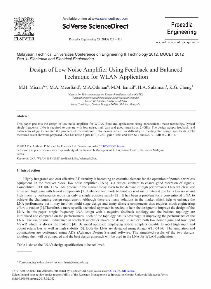
1.1 Feedback amplifier design
In low noise amplifier design, it is often requires both low noise figure and low input voltage standing wave ratio(VSWR). However, there is tradeoff between these two parameters as the source reflection coefficient required for an inputconjugate match ( m) and the source reflection coefficient required for minimum noise ( opt) are always not equal.Therefore, there exists the problem where the input matching network cannot achieve low VSWR and low noise figuresimultaneously [4]. However, by using the series feedback techniques, this problem can be solved and it has threepredominant effects such as increased input resistance, increased in band stability and increased gain [4]. Typically the inductance can be inserted by grounding the transistor through a short transmission line or by adding small value of inductor to the ground [2]. The adding of inductance moves the reflection coefficient required for an input conjugate match closer to
opt. Figure 1 shows that an ideal inductor is added in series with the source lead of the FET which is also known as negativeseries feedback technique.
Fig. 1. FET model with external source inductance [4]
The voltage developed accross the internal Cgs capacitor is
where S is the complex frequency variable
Substituting
for Is gives:
(1)
(2)
(3)
(4)
325 M.H. Misran et al. / Procedia Engineering 53 ( 2013 ) 323 – 331
(5)
Again, substituting for and dividing through by gives:
Canceling out in the last term yields the result:
Substituting S = jw into the above equation gives the input impedance as a function of frequency. This is the new composite FET input impedance.
Equation 7 (FET with feedback) can be rewritten as follows:
The impedance of FET without feedback can be written
By comparing the equation 8 (with feedback) and equation 9 (without feedback), it can be seen that feedback adds [Ra +input impedance [4]. From the derivation above, it can be seen that the use of feedback, adds a real
(resistive) component of Ra and also a positive reactive component. Both of these effects move Zin* closer to opt. This happens as optremain unchanged with the addition of source inductance. Therefore, ast Zin* moves closer to opt, the distance between the noise match and the gain match get closer in the smith chart, facilitating a simultaneous gain and noisematch [4].
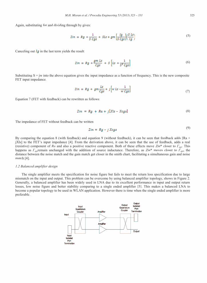
1.2 Balanced amplifier design
The single amplifier meets the specification for noise figure but fails to meet the return loss specification due to largemismatch on the input and output. This problem can be overcome by using balanced amplifier topology, shows in Figure 2.Generally, a balanced amplifier has been widely used in LNA due to its excellent performance in input and output returnlosses, low noise figure and better stability comparing to a single ended amplifier [5]. This makes a balanced LNA tobecome a popular topology to be used in WLAN application. However there is time when the single ended amplifier is morepreferable.
(6)
(7)
(8)
(9)
326 M.H. Misran et al. / Procedia Engineering 53 ( 2013 ) 323 – 331
Fig. 2. Block diagram of a balanced amplifier
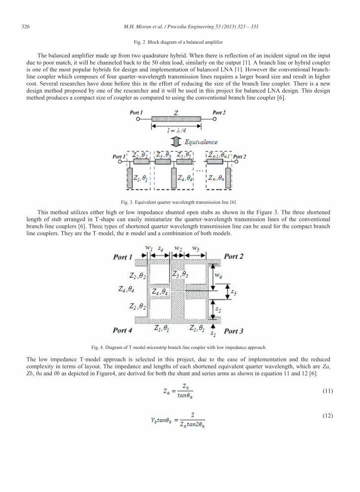
The balanced amplifier made up from two quadrature hybrid. When there is reflection of an incident signal on the input due to poor match, it will be channeled back to the 50 ohm load, similarly on the output [1]. A branch line or hybrid coupler is one of the most popular hybrids for design and implementation of balanced LNA [1]. However the conventional branch-line coupler which composes of four quarter-wavelength transmission lines requires a larger board size and result in higher cost. Several researches have done before this in the effort of reducing the size of the branch line coupler. There is a new design method proposed by one of the researcher and it will be used in this project for balanced LNA design. This design method produces a compact size of coupler as compared to using the conventional branch line coupler [6].
Fig. 3. Equivalent quarter wavelength transmission line [6]
This method utilizes either high or low impedance shunted open stubs as shown in the Figure 3. The three shortened length of stub arranged in T-shape can easily miniaturize the quarter-wavelength transmission lines of the conventionalbranch-line couplers [6]. Three types of shortened quarter wavelength transmission line can be used for the compact branchline couplers. They are the T- -model and a combination of both models.
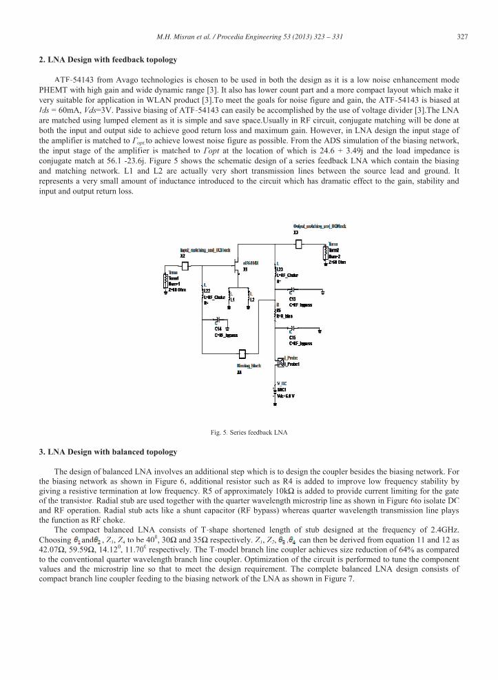
Fig. 4. Diagram of T-model microstrip branch line coupler with low impedance approach
The low impedance T-model approach is selected in this project, due to the ease of implementation and the reduced complexity in terms of layout. The impedance and lengths of each shortened equivalent quarter wavelength, which are Za,Zb, a and as depicted in Figure4, are derived for both the shunt and series arms as shown in equation 11 and 12 [6].
(11)
(12)
327 M.H. Misran et al. / Procedia Engineering 53 ( 2013 ) 323 – 331
2. LNA Design with feedback topology
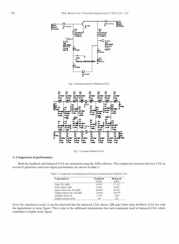
ATF-54143 from Avago technologies is chosen to be used in both the design as it is a low noise enhancement modePHEMT with high gain and wide dynamic range [3]. It also has lower count part and a more compact layout which make itvery suitable for application in WLAN product [3].To meet the goals for noise figure and gain, the ATF-54143 is biased at IdsII = 60mA, Vds=3V. Passive biasing of ATF-54143 can easily be accomplished by the use of voltage divider [3].The LNAare matched using lumped element as it is simple and save space.Usually in RF circuit, conjugate matching will be done atboth the input and output side to achieve good return loss and maximum gain. However, in LNA design the input stage of the amplifier is matched to opt.to achieve lowest noise figure as possible. From the ADS simulation of the biasing network,the input stage of the amplifier is matched toff at the location of which is 24.6 + 3.49j and the load impedance isconjugate match at 56.1 -23.6j. Figure 5 shows the schematic design of a series feedback LNA which contain the biasingand matching network. L1 and L2 are actually very short transmission lines between the source lead and ground. It represents a very small amount of inductance introduced to the circuit which has dramatic effect to the gain, stability and input and output return loss.
Fig. 5. Series feedback LNA
3. LNA Design with balanced topology
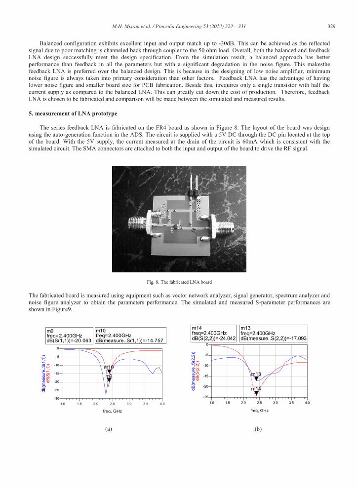
The design of balanced LNA involves an additional step which is to design the coupler besides the biasing network. For the biasing network as shown in Figure 6, additional resistor such as R4 is added to improve low frequency stability by
of the transistor. Radial stub are used together with the quarter wavelength microstrip line as shown in Figure 6to isolate DCand RF operation. Radial stub acts like a shunt capacitor (RF bypass) whereas quarter wavelength transmission line playsthe function as RF choke.
The compact balanced LNA consists of T-shape shortened length of stub designed at the frequency of 2.4GHz. Choosing and , Z3Z , Z4ZZ to be 400 Z1Z , Z2Z , , can then be derived from equation 11 and 12 as
0, 11.700 respectively. The T-model branch line coupler achieves size reduction of 64% as comparedto the conventional quarter wavelength branch line coupler. Optimization of the circuit is performed to tune the componentvalues and the microstrip line so that to meet the design requirement. The complete balanced LNA design consists of compact branch line coupler feeding to the biasing network of the LNA as shown in Figure 7.
328 M.H. Misran et al. / Procedia Engineering 53 ( 2013 ) 323 – 331
Fig. 6. Biasing network of balanced LNA
Fig. 7. Compact balanced LNA
4. Comparison of performance
Both the feedback and balanced LNA are simulated using the ADS software. The comparison between this two LNA in several S-parameter and noise figure performance are shown in table 2.
Table 2. Comparison of simulated result between balanced and feedback LNA
S-parameters Feedback LNA
Balanced LNA
Gain, S21 (dB) 14.951 17.112Noise figure (dB) 0.663 0.846Input return loss, S11(dB) -20.063 -30.412Output return loss, S22(dB) -24.042 -30.679Stability factor, K 1.334 1.263Supply current (mA) 60 120
From the simulation result, it can be observed that the balanced LNA shows 2dB gain better than feedback LNA but withthe degradation in noise figure. This is due to the additional transmission line and component used in balanced LNA whichcontribute to higher noise figure.
329 M.H. Misran et al. / Procedia Engineering 53 ( 2013 ) 323 – 331
Balanced configuration exhibits excellent input and output match up to -30dB. This can be achieved as the reflected signal due to poor matching is channeled back through coupler to the 50 ohm load. Overall, both the balanced and feedback LNA design successfully meet the design specification. From the simulation result, a balanced approach has better performance than feedback in all the parameters but with a significant degradation in the noise figure. This makesthe feedback LNA is preferred over the balanced design. This is because in the designing of low noise amplifier, minimum noise figure is always taken into primary consideration than other factors. Feedback LNA has the advantage of having lower noise figure and smaller board size for PCB fabrication. Beside this, itrequires only a single transistor with half the current supply as compared to the balanced LNA. This can greatly cut down the cost of production. Therefore, feedback LNA is chosen to be fabricated and comparison will be made between the simulated and measured results.
5. measurement of LNA prototype
The series feedback LNA is fabricated on the FR4 board as shown in Figure 8. The layout of the board was design using the auto-generation function in the ADS. The circuit is supplied with a 5V DC through the DC pin located at the top of the board. With the 5V supply, the current measured at the drain of the circuit is 60mA which is consistent with the simulated circuit. The SMA connectors are attached to both the input and output of the board to drive the RF signal.
Fig. 8. The fabricated LNA board
The fabricated board is measured using equipment such as vector network analyzer, signal generator, spectrum analyzer and noise figure analyzer to obtain the parameters performance. The simulated and measured S-parameter performances are shown in Figure9.
1.5 2.0 2.5 3.0 3.51.0 4.0
-25
-20
-15
-10
-5
-30
0
freq, GHz
dB(S
(1,1
))
m9
dB(m
easu
re..S
(1,1
))
m10
m9freq=dB(S(1,1))=-20.063
2.400GHzm10freq=dB(measure..S(1,1))=-14.757
2.400GHz
1.5 2.0 2.5 3.0 3.51.0 4.0
-20
-15
-10
-5
-25
0
freq, GHz
dB
(S(2
,2))
m14dB
(measu
re..S
(2,2
))
m13
m14freq=dB(S(2,2))=-24.042
2.400GHzm13freq=dB(measure..S(2,2))=-17.093
2.400GHz
(a) (b)
330 M.H. Misran et al. / Procedia Engineering 53 ( 2013 ) 323 – 331
1.5 2.0 2.5 3.0 3.51.0 4.0
-10
0
10
-20
20
freq, GHz
dB
(S(2
,1))
m4
dB
(measu
re..S
(2,1
)) m8
m4freq=dB(S(2,1))=14.951
2.400GHzm8freq=dB(measure..S(2,1))=10.024
2.400GHz
1.5 2.0 2.5 3.0 3.51.0 4.0
-60
-50
-40
-30
-20
-70
-10
freq, GHz
dB
(S(1
,2))
m11
dB
(measu
re..S
(1,2
))
m12
m11freq=dB(S(1,2))=-22.060
2.400GHzm12freq=dB(measure..S(1,2))=-18.489
2.400GHz
(c) (d)
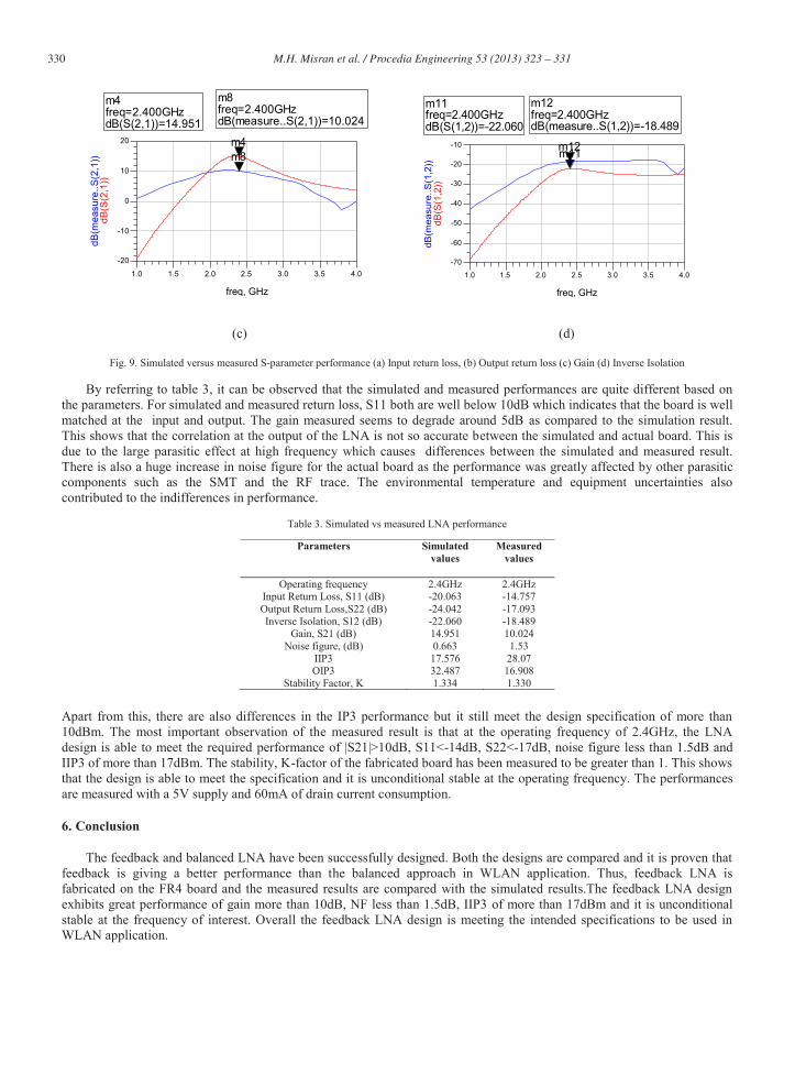
Fig. 9. Simulated versus measured S-parameter performance (a) Input return loss, (b) Output return loss (c) Gain (d) Inverse Isolation
By referring to table 3, it can be observed that the simulated and measured performances are quite different based on the parameters. For simulated and measured return loss, S11 both are well below 10dB which indicates that the board is well matched at the input and output. The gain measured seems to degrade around 5dB as compared to the simulation result. This shows that the correlation at the output of the LNA is not so accurate between the simulated and actual board. This is due to the large parasitic effect at high frequency which causes differences between the simulated and measured result. There is also a huge increase in noise figure for the actual board as the performance was greatly affected by other parasitic components such as the SMT and the RF trace. The environmental temperature and equipment uncertainties also contributed to the indifferences in performance.
Table 3. Simulated vs measured LNA performance
Apart from this, there are also differences in the IP3 performance but it still meet the design specification of more than 10dBm. The most important observation of the measured result is that at the operating frequency of 2.4GHz, the LNA design is able to meet the required performance of |S21|>10dB, S11<-14dB, S22<-17dB, noise figure less than 1.5dB and IIP3 of more than 17dBm. The stability, K-factor of the fabricated board has been measured to be greater than 1. This shows that the design is able to meet the specification and it is unconditional stable at the operating frequency. The performances are measured with a 5V supply and 60mA of drain current consumption.
6. Conclusion
The feedback and balanced LNA have been successfully designed. Both the designs are compared and it is proven that feedback is giving a better performance than the balanced approach in WLAN application. Thus, feedback LNA is fabricated on the FR4 board and the measured results are compared with the simulated results.The feedback LNA design exhibits great performance of gain more than 10dB, NF less than 1.5dB, IIP3 of more than 17dBm and it is unconditional stable at the frequency of interest. Overall the feedback LNA design is meeting the intended specifications to be used in WLAN application.
Parameters Simulated values
Measured values
Operating frequency 2.4GHz 2.4GHz Input Return Loss, S11 (dB) -20.063 -14.757 Output Return Loss,S22 (dB) -24.042 -17.093 Inverse Isolation, S12 (dB) -22.060 -18.489
Gain, S21 (dB) 14.951 10.024 Noise figure, (dB) 0.663 1.53
IIP3 17.576 28.07 OIP3 32.487 16.908
Stability Factor, K 1.334 1.330
331 M.H. Misran et al. / Procedia Engineering 53 ( 2013 ) 323 – 331
For further improvement study and future work, it is recommended that a comparison is made with the cascoded LNA design as it is proven to exhibit a higher gain due to increase in the output impedance as well as better isolation between the input and output ports. Cascoded LNA also improved bandwidth due to reduced Miller capacitance associated with the input time constant. Also a method of moment with an EM simulator can be added in the simulation stage to improve the correlations between the simulated and measured result.
Acknowledgements
The author would like to thank to lab assistance in UTeM for their guidance and technical support and UTeM for supporting this project and also for financing this conference. References [1] D. M. Pozar, Microwave and RF Design of Wireless Systems. 3rd Edition: John Wiley & Sons Inc, 2001. [2] Av -
Technologies, USA, Tech. AV01-0602EN August 5, 2008. [3] S. Liao, Microwave Circuit Analysis and Amplifier Design, Prentice-Hall, 2001. [4] D. D. Henkes. LNA Design Uses Series Feedback to Achieve Simultaneous Low Input VSWR and Low Noise. RF Design. July 1998: 26-32 [5] G. Gonzalez, Microwave Transistor Amplifiers. 2ndEdition: Prentice-Hall, 1997 [6] rip Branch- IEEE Transactions
on Microwave Theory and Techniques, Vol. 55, No. 9, September 2007, pp. 1926-1934.


![INTERNATIONAL JOURNAL OF MATERIALS Volume … Malaysia Melaka (UTeM), Hang Tuah Jaya, 76100 Durian Tunggal, ... [22], servo-hydraulic [23], hydro [24], pneumatics [25] and piezoelectric](https://img.pdfslide.us/doc/110x75/5ae637027f8b9a08778cc21c/international-journal-of-materials-volume-malaysia-melaka-utem-hang-tuah.jpg)