Embed Size (px)
Citation preview
Design of an Analog Circuit for use in Brasch Manufacturing’s Prototype Refrigerant Gas Detector
Marc Remmert
4/30/2012
1
Table of Contents
Summary……………………………………………………………………………….. 2
Introduction………………………………………………………………………….. 3
Full Design of Circuit………………………………………………………………. 4
Input Circuit…………………………………………………………………………… 5 - 6
Signal Detection Circuit…………………………………………….. 5
Follower circuit………………………………………..... 5 – 6
Nose Detection Circuit…………………………………………….. 6
Filtering………………………………………………………………………………… 6 - 9
Bandpass Filter…………………………………………………………. 6
Active Filtering Gain…………………………………………………. 7
Follower Circuit………………………………………………………… 8
Filter Casade……………..……………………………………………… 8 - 9
Gain Stage……………………………………………………………………………. 9 - 10
Adjustable Gain………………………………………………………. 9
Active Filtering………………………………………………………… 10
Zero Biasing…………………………………………………………….. 10
Component Analysis……………………………………………………………. 11 - 15
Input stage………………………………………………………………. 11 - 13
Filter Stage………………………………………………………………. 14
Gain Stage………………………………………………………………. 14
Table of Component Values……………………………………. 15
Future Devlopments…………………………………………………………… 16
Appendix…………………………………………………………………………….. 17

2
Summary:
Brasch Manufacturing is seeking to build a new refrigerant gas detector using the photo
acoustic effect and needs an analog circuit for signal filtering and amplification. For my
research project in ESE 497 I designed this analog circuit. This report describes the process of
design, explanation of design decisions and a progress report for the project. The circuit is
broken down into its three stages, input, filter, design, and methods of finding component
values. This circuit is fully designed and has been approved by the engineer at Brasch
overseeing my work. Hardware tests are the next step in the project, before a final design can
be integrated into the prototype gas detector.
3
Design of an Analog Circuit for use in Brasch Manufacturing’s Prototype Refrigerant Gas Detector
Introduction:
Brasch Manufacturing is seeking to design a refrigerant gas detector which utilizes the photo-acoustic
effect. An analog circuit for signal clarification and amplification is necessary in the design of this
detector. For my undergraduate research with the Electrical and Systems Engineering Department I
designed this circuit. The purpose of this report is to detail the reasons for design decisions and the
methodology behind my design, and report on the project’s progress. The design was broken into four
parts, input design, filter design, gain design, and component value calculations. The report will
conclude with the current progress of the project and the future steps.
4
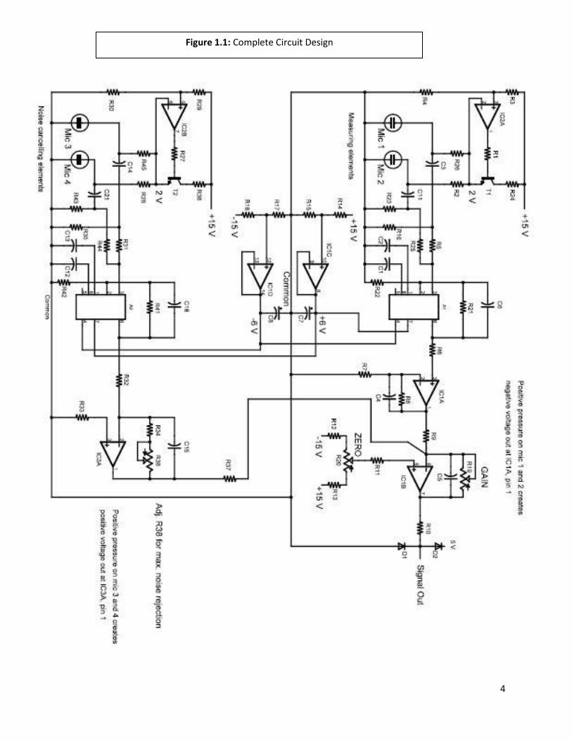
Figure 1.1: Complete Circuit Design
5
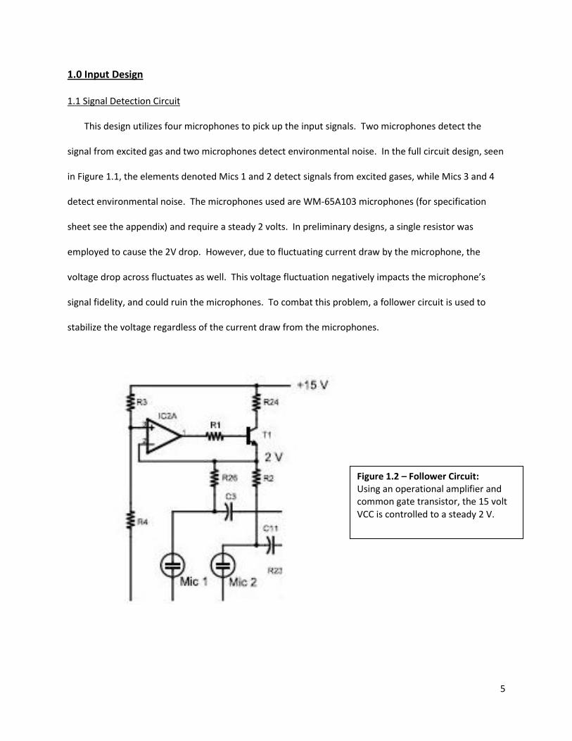
1.0 Input Design
1.1 Signal Detection Circuit
This design utilizes four microphones to pick up the input signals. Two microphones detect the
signal from excited gas and two microphones detect environmental noise. In the full circuit design, seen
in Figure 1.1, the elements denoted Mics 1 and 2 detect signals from excited gases, while Mics 3 and 4
detect environmental noise. The microphones used are WM-65A103 microphones (for specification
sheet see the appendix) and require a steady 2 volts. In preliminary designs, a single resistor was
employed to cause the 2V drop. However, due to fluctuating current draw by the microphone, the
voltage drop across fluctuates as well. This voltage fluctuation negatively impacts the microphone’s
signal fidelity, and could ruin the microphones. To combat this problem, a follower circuit is used to
stabilize the voltage regardless of the current draw from the microphones.
Figure 1.2 – Follower Circuit: Using an operational amplifier and common gate transistor, the 15 volt VCC is controlled to a steady 2 V.
6
The follower circuit utilizes a Texas Instruments Tl062a amplifier; its specifications can be found
in the appendix. In Figure 1.2, this operational amplifier (op amp) is labeled IC2A. This particular model
is used because of its low power consumption. Resistors R3 and R24 are used to drop the 15 volt VCC
down to 2V. The op amp uses a direct negative feedback loop, which forces a unity gain and stable 2V
on the output.
1.2 Noise Detection Circuit
The noise detection circuit is identical to the gas detection circuit. The treatment of these
signals must be the same in order to effectively manipulate them later in the circuit. Therefore, the
resistor values R27, 28, 29, 30, 36, and 45 all have the same value as the corresponding resistors of the
gas detection circuit. It is important to note however, that the signals coming from Mics 1 and 2 will be
very different from those coming from Mics 3 and 4. Using this difference, the frequency components
caused by environmental noise can be canceled before amplification.
2.0 Filtering Stage
Filtering is often done in several steps to ensure proper noise cancellation. One stage filtering does
not perfectly attenuate the unwanted region of the frequency spectrum. Therefore, in this circuit,
filtering occurs over two stages. The gain stage also has filtering properties.
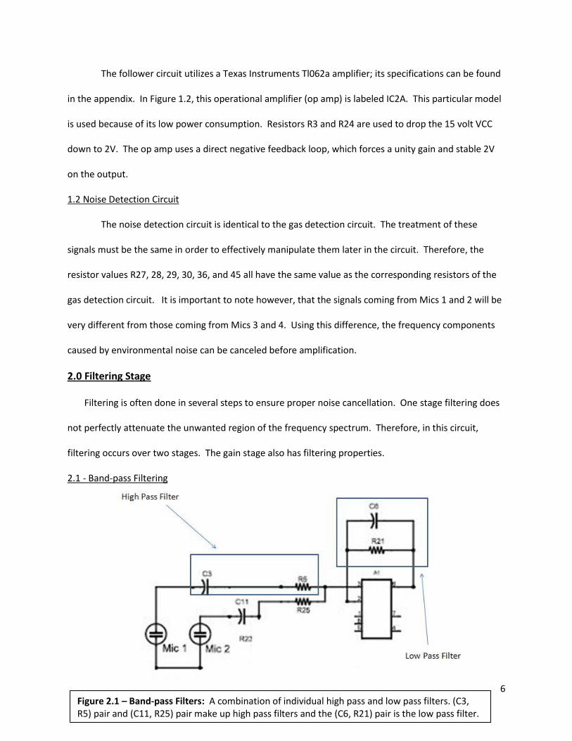
2.1 - Band-pass Filtering
Figure 2.1 – Band-pass Filters: A combination of individual high pass and low pass filters. (C3, R5) pair and (C11, R25) pair make up high pass filters and the (C6, R21) pair is the low pass filter.
7
As seen in Figure 2.1, the input signals are band-pass filtered. This graphic shows the gas
detection circuit which is identical to the noise detection circuitry. The input signals have a frequency of
around 2000Hz. The resonant cell used for trapping the gas has a resonant frequency of 2000Hz, which
causes the frequency pulses to be released at the same frequency. Therefore the band-pass filter must
be centered around 2kHz. The (C3, R5) and (C11, R25) pair are the high pass filters for Mics 1 and 2
respectively. These signals are summed together and low pass filtered through an op amp.
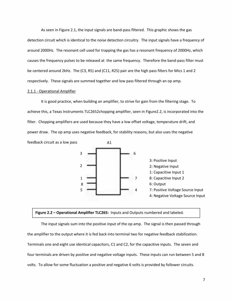
2.1.1 - Operational Amplifier
It is good practice, when building an amplifier, to strive for gain from the filtering stage. To
achieve this, a Texas Instruments TLC2652chopping amplifier, seen in Figure2.2, is incorporated into the
filter. Chopping amplifiers are used because they have a low offset voltage, temperature drift, and
power draw. The op amp uses negative feedback, for stability reasons, but also uses the negative
feedback circuit as a low pass filter.
The input signals sum into the positive input of the op amp. The signal is then passed through
the amplifier to the output where it is fed back into terminal two for negative feedback stabilization.
Terminals one and eight use identical capacitors, C1 and C2, for the capacitive inputs. The seven and
four terminals are driven by positive and negative voltage inputs. These inputs can run between 5 and 8
volts. To allow for some fluctuation a positive and negative 6 volts is provided by follower circuits.
A1
6
7
4
3
2
1
8
5
Figure 2.2 – Operational Amplifier TLC265: Inputs and Outputs numbered and labeled.
3: Positive Input
2: Negative Input
1: Capacitive Input 1
8: Capacitive Input 2
6: Output
7: Positive Voltage Source Input
4: Negative Voltage Source Input
8
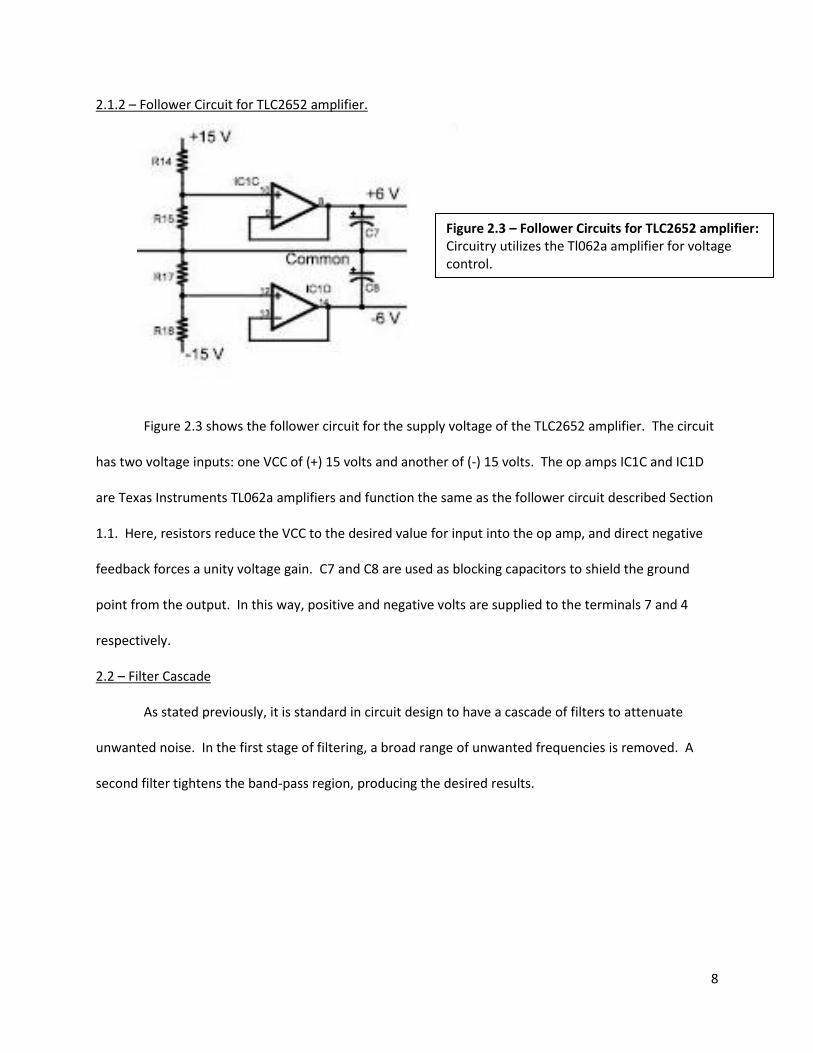
2.1.2 – Follower Circuit for TLC2652 amplifier.
Figure 2.3 shows the follower circuit for the supply voltage of the TLC2652 amplifier. The circuit
has two voltage inputs: one VCC of (+) 15 volts and another of (-) 15 volts. The op amps IC1C and IC1D
are Texas Instruments TL062a amplifiers and function the same as the follower circuit described Section
1.1. Here, resistors reduce the VCC to the desired value for input into the op amp, and direct negative
feedback forces a unity voltage gain. C7 and C8 are used as blocking capacitors to shield the ground
point from the output. In this way, positive and negative volts are supplied to the terminals 7 and 4
respectively.
2.2 – Filter Cascade
As stated previously, it is standard in circuit design to have a cascade of filters to attenuate
unwanted noise. In the first stage of filtering, a broad range of unwanted frequencies is removed. A
second filter tightens the band-pass region, producing the desired results.
Figure 2.3 – Follower Circuits for TLC2652 amplifier: Circuitry utilizes the Tl062a amplifier for voltage control.
9
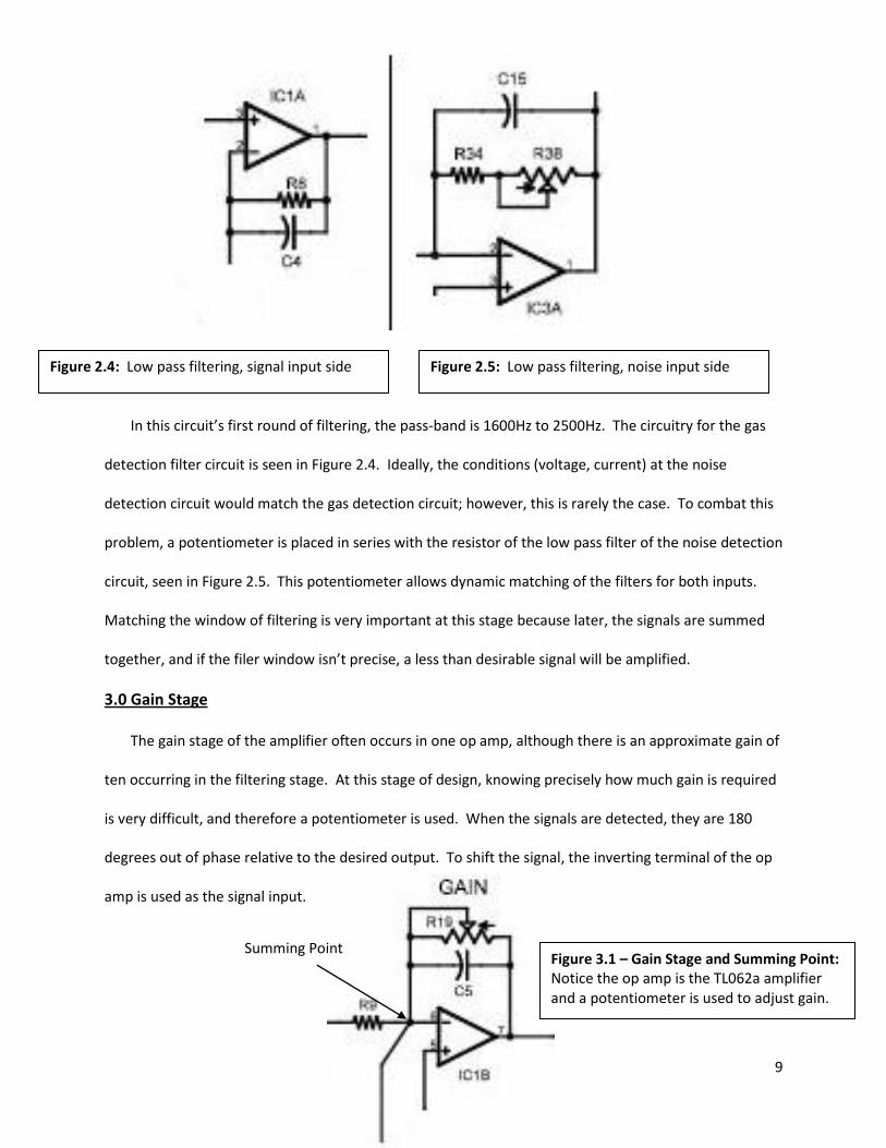
In this circuit’s first round of filtering, the pass-band is 1600Hz to 2500Hz. The circuitry for the gas
detection filter circuit is seen in Figure 2.4. Ideally, the conditions (voltage, current) at the noise
detection circuit would match the gas detection circuit; however, this is rarely the case. To combat this
problem, a potentiometer is placed in series with the resistor of the low pass filter of the noise detection
circuit, seen in Figure 2.5. This potentiometer allows dynamic matching of the filters for both inputs.
Matching the window of filtering is very important at this stage because later, the signals are summed
together, and if the filer window isn’t precise, a less than desirable signal will be amplified.
3.0 Gain Stage
The gain stage of the amplifier often occurs in one op amp, although there is an approximate gain of
ten occurring in the filtering stage. At this stage of design, knowing precisely how much gain is required
is very difficult, and therefore a potentiometer is used. When the signals are detected, they are 180
degrees out of phase relative to the desired output. To shift the signal, the inverting terminal of the op
amp is used as the signal input.
Figure 2.4: Low pass filtering, signal input side Figure 2.5: Low pass filtering, noise input side
Summing Point Figure 3.1 – Gain Stage and Summing Point: Notice the op amp is the TL062a amplifier and a potentiometer is used to adjust gain.
10
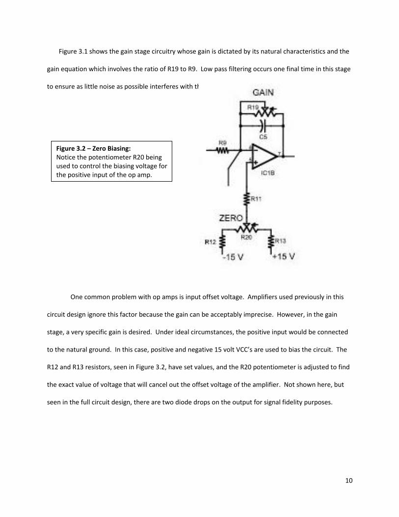
Figure 3.1 shows the gain stage circuitry whose gain is dictated by its natural characteristics and the
gain equation which involves the ratio of R19 to R9. Low pass filtering occurs one final time in this stage
to ensure as little noise as possible interferes with the amplification.
One common problem with op amps is input offset voltage. Amplifiers used previously in this
circuit design ignore this factor because the gain can be acceptably imprecise. However, in the gain
stage, a very specific gain is desired. Under ideal circumstances, the positive input would be connected
to the natural ground. In this case, positive and negative 15 volt VCC’s are used to bias the circuit. The
R12 and R13 resistors, seen in Figure 3.2, have set values, and the R20 potentiometer is adjusted to find
the exact value of voltage that will cancel out the offset voltage of the amplifier. Not shown here, but
seen in the full circuit design, there are two diode drops on the output for signal fidelity purposes.
Figure 3.2 – Zero Biasing: Notice the potentiometer R20 being used to control the biasing voltage for the positive input of the op amp.
11
4.0 Determining Component Values
4.1 Input components
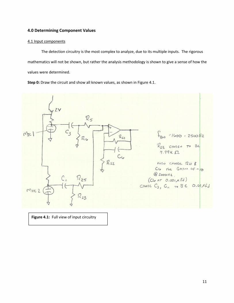
The detection circuitry is the most complex to analyze, due to its multiple inputs. The rigorous
mathematics will not be shown, but rather the analysis methodology is shown to give a sense of how the
values were determined.
Step 0: Draw the circuit and show all known values, as shown in Figure 4.1.
Figure 4.1: Full view of input circuitry
12
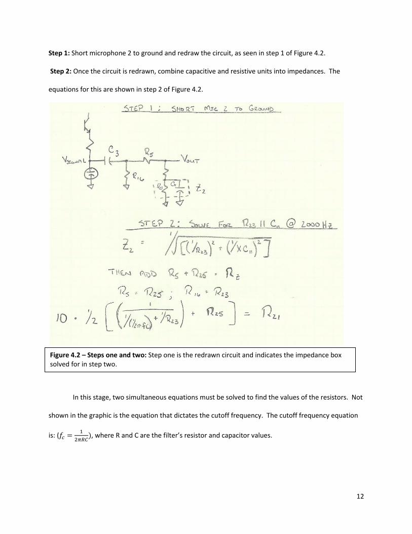
Step 1: Short microphone 2 to ground and redraw the circuit, as seen in step 1 of Figure 4.2.
Step 2: Once the circuit is redrawn, combine capacitive and resistive units into impedances. The
equations for this are shown in step 2 of Figure 4.2.
In this stage, two simultaneous equations must be solved to find the values of the resistors. Not
shown in the graphic is the equation that dictates the cutoff frequency. The cutoff frequency equation
is: (
, where R and C are the filter’s resistor and capacitor values.
Figure 4.2 – Steps one and two: Step one is the redrawn circuit and indicates the impedance box solved for in step two.
13
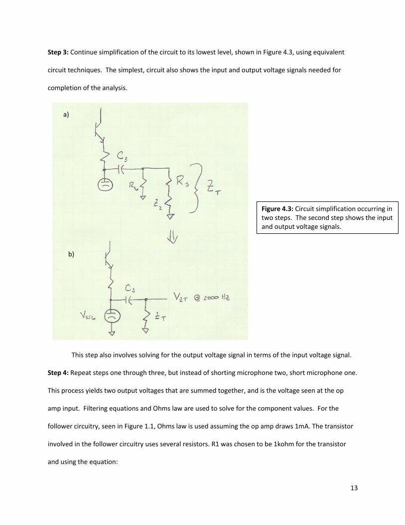
Step 3: Continue simplification of the circuit to its lowest level, shown in Figure 4.3, using equivalent
circuit techniques. The simplest, circuit also shows the input and output voltage signals needed for
completion of the analysis.
This step also involves solving for the output voltage signal in terms of the input voltage signal.
Step 4: Repeat steps one through three, but instead of shorting microphone two, short microphone one.
This process yields two output voltages that are summed together, and is the voltage seen at the op
amp input. Filtering equations and Ohms law are used to solve for the component values. For the
follower circuitry, seen in Figure 1.1, Ohms law is used assuming the op amp draws 1mA. The transistor
involved in the follower circuitry uses several resistors. R1 was chosen to be 1kohm for the transistor
and using the equation:
Figure 4.3: Circuit simplification occurring in two steps. The second step shows the input and output voltage signals.
a)
b)
14
where Beta is approximately 99 for this transistor. Therefore
R2, and R26 are one tenth of R1.
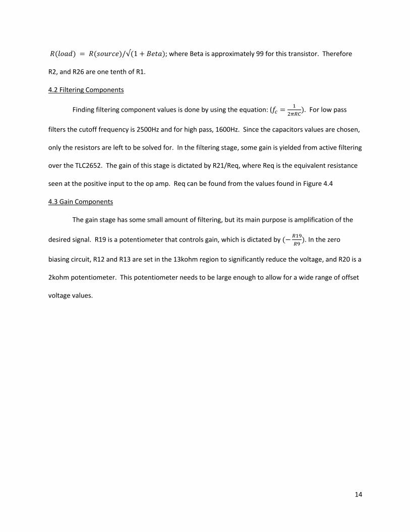
4.2 Filtering Components
Finding filtering component values is done by using the equation: (
. For low pass
filters the cutoff frequency is 2500Hz and for high pass, 1600Hz. Since the capacitors values are chosen,
only the resistors are left to be solved for. In the filtering stage, some gain is yielded from active filtering
over the TLC2652. The gain of this stage is dictated by R21/Req, where Req is the equivalent resistance
seen at the positive input to the op amp. Req can be found from the values found in Figure 4.4
4.3 Gain Components
The gain stage has some small amount of filtering, but its main purpose is amplification of the
desired signal. R19 is a potentiometer that controls gain, which is dictated by
. In the zero
biasing circuit, R12 and R13 are set in the 13kohm region to significantly reduce the voltage, and R20 is a
2kohm potentiometer. This potentiometer needs to be large enough to allow for a wide range of offset
voltage values.
15
Components Values
R3, 29 13kohm
R24,36 13kohm
R1,27 1kohm
R2,28 100ohm
R26,45 100ohm
R4,30 2kohm
R5,31 16.2kohm
R25,44 16.2kohm
R22, 42 4.99kohm
R23,43 6.19kohm
R16, 35 6.19kohm
R21,41 63.4kohm
R6,32 1kohm
R7, 33 1kohm
R8 63.4kohm
R9 1kohm
R34 60kohm
R38,19,20 Adjustable
R11 1kohm
R12,13 13kohm
R10 1kohm
R14,17 9kohm
R15,18 6kohm
C3,14 0.01ufd
C11,21 0.01ufd
C2,13 0.1ufd
C1,12 0.1ufd
C6,18 0.001ufd
C4,15 0.00ufd
C7,8 100ufd
C5 .001ufd
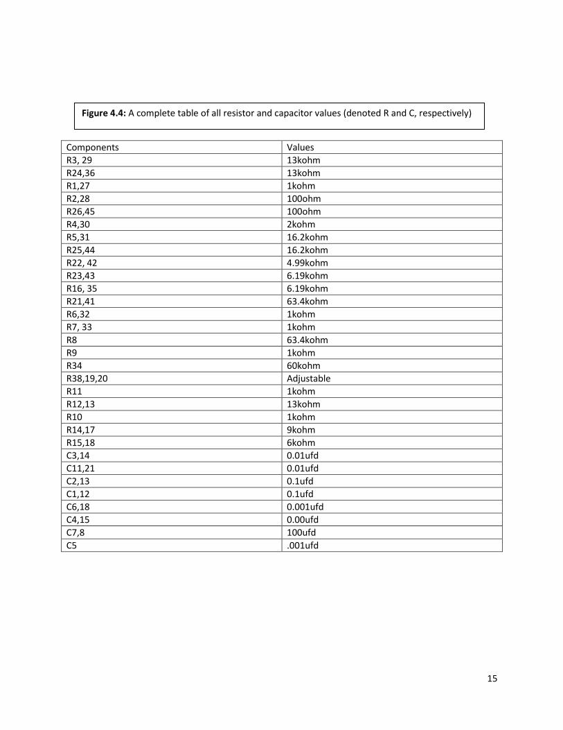
Figure 4.4: A complete table of all resistor and capacitor values (denoted R and C, respectively)
16
5.0 Progress and the Future of the Project
This circuit is fully designed and has been approved by Dan Newhouse, the Brasch Engineer over
seeing my design. The next step of this project is to construct a prototype circuit and test it, as
hardware tests often reveal hidden issues. Once all the bugs have been worked out of the system, the
circuit will be fabricated and tested on the fabricated board. Eventually, the board will be integrated
into the full design of the Brasch refrigerant gas detector.
Concluding Remarks:
I would like to thank Brasch Manufacturing and the Preston M. Green Department of Electrical
and Systems engineering for the experience of getting to work on this project. It seems seldom to
students get the chance to work on real world applications, and I am very grateful for this invaluable
experience. I will be working with Brasch Manufacturing this summer to continue work on this
prototype detector and am excited for the opportunity to apply the knowledge I have gained from the
department through classes and this research project at Brasch.
17
Appendix
TLC2652 Specification Sheet
Tl062a Specification Sheet
WM-65A103 Microphone Specification Sheet