Embed Size (px)
Citation preview
Design of a Silicon-based Optical Neural Network
Danni Zhang1,2, Pengfei Wang1,3, Guangzhen Luo1,3, Yu Bi1,3, Ye Zhang2, Junkai Yi2, Yanmei Su1, Yejin Zhang1,3 and Jiaoqing Pan1,3,*
1Institute of Semiconductors, Chinese Academy of Sciences, Beijing, China 2School of Automation, Beijing Information Science and Technology University, Beijing 100192, China
3College of Materials Science and Opto-Electronic Technology, University of Chinese Academy of Sciences, Beijing, China *Corresponding author
Abstract—In this paper, a silicon-based fully connected optical neural network (ONN) is designed, which can be use to image classification and recognition with accuracy greater than 97%. A fully connected neural network is constructed. One layer model has been used in chip design. Chip simulation shows accuracy could not be impacted as photons large enough. This structure could be used in deep learning.
Keywords—optical neural network; simulation; SiN; chip design; neuromorphic computing
I. INTRODUCTION
Since it is an information explosion world, more and more information needs to be processed, while the current technology limits the development. Optical processors are slowly gaining traction. In order to run more data, we need more fast, low-power, small-scale devices, and optical processors are gaining attention. In the human brain, there are about 1011 neurons and 1015 synapses, which occupy only small position and consume very little power. In addition, the human brain is considered to be the smartest and fastest operate system.[1] At present, many studies aim to create neural network circuits to simulate the brain. But conventional electronics tend to block the extremely complex wiring required for neural networks, while using light energy can eliminate the interference caused by electric charges and allow signals to travel farther. Compared with electronics, optics has obvious advantages of low power consumption and low latency, which is important for artificial intelligence.
In 2016, Alexandria et al. introduced the world's first photonic neural network.[2] In 2017, Yichen Shen's chip implemented a neural network that can recognize four basic vowels. Even though the system is still fairly basic, it has 77 percent accuracy of that time, compared with nearly 90 percent by traditional methods.[3] In 2019, Feldmann et al. realized small-scale supervised learning and unsupervised learning on the devices they made.[4]In our work, an image classification and recognition model based on the fully connected neural network is designed, which is mapped to the silicon-based photonic integrated link. The recognition accuracy of this chip is simulated by using Python in the Linux system, and Optical modulator makes this chip has the function of fast and high accuracy classification for hand-writing numbers.
II. FULLY CONNECTIVE NEURAL NETWORK(FCNN)
STRUCTURE
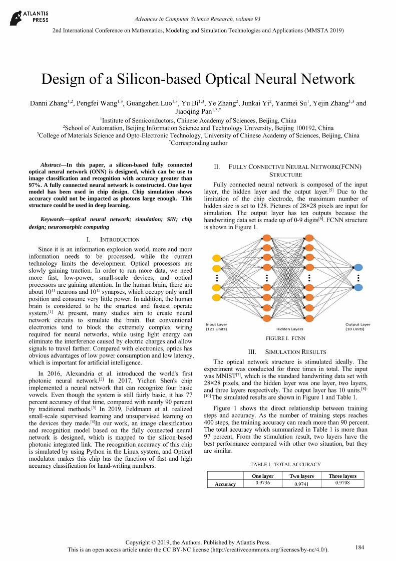
Fully connected neural network is composed of the input layer, the hidden layer and the output layer.[5] Due to the limitation of the chip electrode, the maximum number of hidden size is set to 128. Pictures of 28×28 pixels are input for simulation. The output layer has ten outputs because the handwriting data set is made up of 0-9 digits[6]. FCNN structure is shown in Figure 1.
FIGURE I. FCNN
III. SIMULATION RESULTS
The optical network structure is stimulated ideally. The experiment was conducted for three times in total. The input was MNIST[7], which is the standard handwriting data set with 28×28 pixels, and the hidden layer was one layer, two layers, and three layers respectively. The output layer has 10 units.[8]-
[10] The simulated results are shown in Figure 1 and Table 1.
Figure 1 shows the direct relationship between training steps and accuracy. As the number of training steps reaches 400 steps, the training accuracy can reach more than 90 percent. The total accuracy which summarized in Table 1 is more than 97 percent. From the stimulation result, two layers have the best performance compared with other two situation, but they are similar.
TABLE I. TOTAL ACCURACY
One layer Two layers Three layers
Accuracy 0.9736 0.9741 0.9708
2nd International Conference on Mathematics, Modeling and Simulation Technologies and Applications (MMSTA 2019)
Copyright © 2019, the Authors. Published by Atlantis Press. This is an open access article under the CC BY-NC license (http://creativecommons.org/licenses/by-nc/4.0/).
Advances in Computer Science Research, volume 93
184

FIGURE II. SIMULATION ACCURACY
IV. SI-BASED ONN CHIP DESIGN
Part III is shown that the total accuracy of each experiment is almost similar. For future scalability and optical device limitations, a layer network for chip design has been used.
The silicon-based ONN chip is mainly composed of five parts. The input port is the first, which can be realized by edge coupler or grating coupler. The fan out structure can be realized by cascaded 1×2 MMI, which divides the input light into 128 parts, followed by an MZM in every two channels. Next, there are 256 MZMs, half of which are used to encode target files, and the other half are used to load weight signals. Then, the paired structure of target file signal and weight signal is realized by two wave-guides: one is silicon wave guide and the other is SiN wave-guide. Finally, there are 128 balance detectors and each balance detector realizes multiplication of one way target file signal and weight signal. The final addition and activation functions can be implemented through circuits. As shown in Figure 3.
FIGURE III. CHIP DESIGN
First, the images are converted into impulse signal and enter the chip by port 1, and then pulse multiplies and adds the trained weights in the chip. After output, the nonlinear computing was operated in computer, and then the final result is obtained.
V. CHIP SIMULATION
Different from the ideal neural network structure, the chips have reasons of impacting accuracy. The reasons mainly exist in the following three aspects: (1) craft precision (2) photon
loss (3) noise. Quantum-limit noise is root of fundamental limit for optical devices. In this part, we will stimulate noise error.
In a neural network, each layer of neurons xi passes to the next layer of neurons. Each neuron is a homodyne detector that interferes with the broadcast signal to the weight signal Aij. Aij
and xi multiply and accumulate (MAC).[11] As equation(1) shows
ixAx iji 1 (1)
xi+1 is the output of current layer.
Assume that there is a perfect spatio-temporal pattern match between the input signal and the weight signal and standardize it, so that ||xi||, ||Aij|| correspond to the photon number of each pulse. The following equation (2) represents the noise added from each layer to the next[3].
AC21
' M
iijin
N
NN
xAwxAx
i (2)
In equation (2), the wi(k)~N(0,1) are Gaussian random
variables, ||· || is the L2 norm, and nMAC is the number of photons per MAC, related to the total energy consumption of the layer by ntot =NN'nMAC
[3],N is the number of input neurons and N' is the number of output neurons.
Then we simulate one layer model as shown in part II with shot noise. Figure 4 demonstrates that accuracy could not be impacted as Photon/nMAC large enough. Error rate decreased as Photon/nMAC = 10-1. As Photon/nMAC = 100, error rate was steady as the best.
FIGURE IV. STIMULATION ERROR RATE
VI. CONCLUSION
In this paper, a image classification and recognition model based on fully connected neural network has been presented. Through simulation, one layer model in our chip design is used.
Advances in Computer Science Research, volume 93
185
It can be mapped to the silicon-based photonic integrated link, and the principle verifies that the chip has the function of fast and high accuracy classification for writing digital data. Silicon-based ONN chip with five parts is designed. Last but not least, we add shot noise into simulation. We found that if photons are huge, the accuracy of neural network could not be influenced.
ACKNOWLEDGMENT
Danni Zhang and Pengfei Wang contribute equally to this paper. This work is supported by NSFC (Grant Nos. 61934007,61974141),BMNSFC (Grants No 4182064) and the Supplementary and Supportive Project for Teachers at Beijing Information Science and Technology University (2019-2021).
REFERENCES [1] Sun Gil Kim, Ji Su Han, Hyojung Kim, Soo Young Kim,Ho Won
Jang.“Recent Advances in Memristive Materials for Artificial Synapses.” Advanced Materials Technologies, 2018,3(12).
[2] Tait A N, Zhou E, De Lima T F, et al., “Neuromorphic Silicon Photonics.” 2016..
[3] Hamerly R, Sludds A, Bernstein L, et al.“ Large-Scale Optical Neural Networks based on Photoelectric Multiplication.”Computers, Networks & Communications, 2018.
[4] Feldmann J et al..,“All-optical spiking neurosynaptic networks with self-learning capabilities.” Nature, 2019,569(7755)..
[5] Hsu, K. Y., H. Y. Li, and D. Psaltis . "Holographic implementation of a fully connected neural network." Proceedings of the IEEE 78.10(1990):1637-1645.
[6] Hinton G, Vinyals O, Dean J. Distilling the Knowledge in a Neural Network[J]. Computer Science, 2015, 14(7):38-39.
[7] The MNIST database of handwritten digits was donloaded from http://yann.lecun.com/exdb/mnist/.
[8] Wu, Shixiao, W. Wei , and L. Zhang.,“Comparison of Machine Learning Algorithms for Handwritten Digit Recognition, 2017.
[9] Bottou, Léon, et al. "Comparison of classifier methods: a case study in handwritten digit recognition." International Conference on Pattern Recognition IEEE Computer Society, 1994.
[10] Dan Claudiu Cireşan, Meier U , Gambardella L M , et al. Deep, Big, Simple Neural Nets for Handwritten Digit Recognition[J]. Neural Computation, 2010, 22(12):3207-3220.
[11] Haykin S. Neural Networks: A Comprehensive Foundation[J]. Neural
[12] Networks A Comprehensive Foundation, 1994:71-80.
Advances in Computer Science Research, volume 93
186