Embed Size (px)
Citation preview

Design of a Novel Transistor and a Microwave Pallet
& Testing of a Novel Power Amplifier
PRIYAM RASTOGI
Master of Science Thesis
Stockholm, Sweden 2012
Design of a Novel Transistor and a Microwave Pallet
& Testing of a Novel Power Amplifier
Priyam Rastogi [email protected]
Examiner: Prof. Li-Rong Zheng Supervisor: Zhuo Zou
Kungliga Tekniska Högskolan Stockholm, Sweden
Supervisor: Freek Van Straten NXP Semiconductors B.V
Nijmegen, The Netherlands
Master of Science Thesis
KTH,ICT Department of Electronic System
SE-164 40 STOCKHOLM


1
SAMMANFATTNING
Radiofrekvens baserad teknik har utlöst ett stort område inom forskning och utveckling. Denna
avhandling arbete bygger på RF krafttransistorer och deras sedvänjor i olika tillämpningar.
Traditionellt har RF-transistorer som används i applikationer basstationer. Men nu är de som
används i nya applikationer som mikrovågstillämpningar, medicinsk utrustning, energikällor för
kapning av trä, torkning kläder och för offentlig belysning. Därför designa RF transistorer krävs
för att göra dem lämpliga för deras nya program. Avhandlingen fokuserar på att bygga mycket
effektiva och billigt RF transistorer och RF förstärkare genom omkonstruktion flera avsnitt av
dem. Rapporten är indelad i tre sektioner.
Den första delen beskriver en ny RF-transistor från design till slutlig testfas. Förpackningen stil
nya RF-effekttransistor modifieras genom att använda olika material för att göra förpackningar
enklare och tillverkningsprocess mer effektiv. Den modifierade RF-transistorn visade positiva
resultat, medan testning som styrker möjligheten att använda det nya paketet för RF-transistor.
Den andra delen av rapporten beskriver en mikrovågsugn pall omdesignad genom att anpassa
transistorn byggd i det första avsnittet. Detta omkonstruktion har en extra fördel av enkelhet,
färre steg tillverkning och låg kostnad. Denna mikrovågsugn pall har en bandbredd på drift från
2900MHz till 3300MHz. Liknande till transistorn har mikrovågsugn pall förpackningen stil
omgjorda utan att påverka dess elektriska beteende. Pallen visade positiva resultat, medan
testning, vilket visar på genomförbarheten av denna nya design.
Den sista delen av rapporten beskriver testning av en ny effektförstärkare. Syftet med detta test
var att observera effekten på olika delar av effektförstärkaren under avlägsnande av cirkulatorn
från det. Testet utfördes för att minska kostnaderna och storleken hos effektförstärkaren. Testet
var inte helt lyckad indikerar behovet av omkonstruktion effektförstärkaren. Arbetet som
presenteras i denna rapport representerar inledande forskning som behöver omfattande granskas i
framtiden att minska kostnaderna och tillverkning tiden för RF-produkter.

2

3
ABSTRACT
Radio frequency based technology has unleashed a vast area in research and development. This
thesis work is based on RF power transistors and their usages in different applications.
Traditionally, RF transistors were used in base station applications. But now, they are being used
in new applications like microwave applications, medical equipment, energy sources for cutting
wood, drying clothes, and street lighting systems. Hence redesign of RF transistors is required to
make them suitable for their new applications. The thesis work focuses on building highly
efficient yet cheap RF transistors and RF amplifiers by redesigning several sections of them.
This report is divided into three sections.
The first section describes a novel RF transistor from design to final testing phase. The
packaging style of the new RF power transistor is modified by using different material to make
packaging process simpler and manufacturing process more efficient. The modified RF transistor
showed positive results while testing, thus proving the feasibility of using the new package for
RF transistor.
The second section of the report describes a microwave pallet redesigned by adapting the
transistor built in the first section. This redesigning has an added advantage of simplicity, fewer
manufacturing steps, and low cost. This microwave pallet has a bandwidth of operation from
2900MHz to 3300MHz. Similar to the transistor, the microwave pallet packaging style was
redesigned without affecting its electrical behavior. The pallet showed positive results while
testing, thus proving the feasibility of this new design.
The last section of the report describes the testing of a novel power amplifier. The aim of this test
was to observe the effect on various parts of the power amplifier while removing the circulator
from it. The test was performed to reduce the cost and size of the power amplifier. The test was
not completely successful indicating the need for redesigning the power amplifier. The work
presented in this report represents initial research that needs to be extensively examined in the
future to reduce the cost and manufacturing time of the RF products.

4

5
FOREWORD
I would like to express my gratitude to some of the people without whose help and support I
would not have successfully completed my thesis work. Foremost I would like to sincerely thank
my supervisor in NXP, Freek Van Straten who was there with me in each and every step of my
thesis work. Without his guidance and support it would have been impossible to complete my
work within the given time. His patience to my mistakes and freedom for the decisions helped
me a lot to enhance both my personal and professional personality. Along with him I would like
to thank my examiner Dr. Li-Rong Zheng who gave me the opportunity to do the master thesis in
my university. This opportunity was a great support as without it all my work would have been
in vain.
I would also like to thank my supervisor in KTH, Zhuo Zou who helped me from the process of
registration to the final presentation of the thesis work. He made my thesis work smooth even
when I was doing my thesis miles away from my university. I would also like to thank my course
coordinator May-Britt Eklund-Larson who supported me in each and every administration work
and made my stray in Netherlands comfortable.
I would like to express my gratitude to Paul Hunneman, Huub Keultjes, Hans Marijnissen, Robin
Stenfert, and Tennyson Nguty, in NXP Semiconductor for their ever ready help and guidance in
different steps of my thesis work. They made my thesis work done rapidly without any
hindrance.
I am extremely grateful to my family for their unconditional love, support and inspiration
without which it would have been difficult to complete this work as this spirit.
Last but not least I would like to thank god who is always there with me in every second of my
life.
Priyam Rastogi
Nijmegen, September and 2012

6
7
ABBREVIATIONS
ADS Advance Design System
BJT Bipolar Junction Transistor
DC Direct Current
ESD Electrostatic Discharge
FM Frequency Modulation
HTCC High Temperature Cofired Ceramic
IR Infra Red
LDMOS Laterally Diffused Metal Oxide Semiconductors
MRI Magnetic Resonance Imaging
PA Power Amplifier
PCB Printed Circuit Board
RADAR Radio Detection and Ranging
RF Radio frequency
SMD Surface Mount Device
UHF Ultra High Frequency
VHF Very High Frequency

8
9
TABLE OF CONTENTS
SAMMANFATTNING (SWEDISH) 1
ABSTRACT 3
FOREWORD 5
NOMENCLATURE 7
TABLE OF CONTENTS 9
1 INTRODUCTION 13
2 TRANSISTOR 15
2.1 Introduction of LDMOS 15
2.2 LDMOS transistor background 17
2.3 Packaging Details of Transistor 21
2.4 BLF7G20LS-200 description 24
2.5 New modified Design 26
2.6 Simulations 27
2.6.1 Modified Ring Frame Simulation 32
2.7 Manufacturing Process 34
2.8 Test Results and Conclusion 36
2.9 Future work 38
3 MICROWAVE PALLET 39
3.1 Description of Pallet 39
3.2 New Design 42
3.2.1 Design Approach 42
3.3 Packaging Details 47
3.4 Simulation 48
3.5 Manufacturing 50

10
3.6 Results and discussion 52
3.6.1 Results of test 1 52
3.6.2 Results of test 2 53
3.6.3 Results of test 3 55
3.6.4 Results of test 4 56
3.7 Conclusion and future work 58
4 TESTING OF A POWER AMPLIFIER 61
4.1 Background 61
4.2 Introduction 61
4.3 PA module description 63
4.4 Test setup 64
4.5 Test Procedure 67
4.6 Measurements 67
4.6.1 PA with circulator readings 68
4.6.2 Test without circulator 73
4.6.2.1 50 watts forward power 73
4.6.2.2 100 watts forward power 77
4.6.2.3 150 watts forward power 80
4.6.2.4 200 watts forward power 83
4.6.3 Repeated test attempts 86
4.7 Analysis of results and Future Work 87
4.7.1 Transistor temperature and current consumption curve 89
5 CONCLUSION AND FUTURE WORK 91
6 REFERENCES 93
APPENDIX A: SUPPLEMENTARY INFORMATION 95

11

12
13
1 INTRODUCTION
Wireless communication is the most thriving technological field in the present world. Innovation
in wireless communication is in great demand in the present world of technology. Wireless
communication has a wide area of application like cellular communication, satellite
communication, microwave, medical and research. The history of wireless communication goes
back to 1897 with Guglielmo Marconi‟s invention of radio transmission [20]. Radio transmission
is done using signals with high frequency range of 3 KHz to 300 GHz [21]. This frequency range
is broadly known as Radio Frequency (RF). The wireless radio communication system consists
of mainly transmission and receiving sub system. This system has many small components like
antenna, amplifiers, filters, phase shifter, oscillators and buffers. In wireless communication,
there is a need to generate RF power. The generated low power RF signals are converted to high
power signals with the help RF power amplifiers. These RF power amplifiers are different from
the small signal amplifiers as they work with signal with high power. The RF power amplifiers
need to have high efficiency, good input and output return loss, linearity and high gain [23].
The RF power amplifiers are complicated due to their high operation frequency range. The main
problem with the radio communication is the interferences, small frequency band of operation
and parasitic effects which makes the design of Power Amplifiers very complicated and costly
[13]. Power amplifiers are very important part of the system. From the production point of view
there is a need to reduce the cost of system to attract consumers. This thesis report describes the
work done on certain sections of the power amplifier to reduce the cost. The work done in this
report consists of three parts. (1) Design and manufacturing of a novel RF transistor, (2)
Redesign of a microwave pallet using the novel RF transistor and (3) Testing of amplifier
without the circulator.
The first part of the report contains the design, implementation and manufacturing of a RF
transistor. This design was an initial step for making a complicated power amplifier. This section
of the report describes the design processes involved in the transistor right from the initial stage
till the final testing stage. This RF transistor design had mainly two parts where changes can be
made. One part was to change from the electrical prospects and the other part was the packaging
process. The work done in this report was on the packaging process change. The present
packaging of the transistors is done in multiple steps which is time consuming and costly.
Currently the RF transistors are having lead frames package, which were replaced with PCB
material during this thesis work.
The second section in this report describes the design and manufacturing of the microwave
pallet. Microwave pallets are simple amplifiers which has the 50Ω termination on both the sides.
They are compact and easy to use by the end user. The microwave pallet design had used the
newly designed RF transistor from the first section. This redesigned microwave pallet design had
to be changed to accommodate the newly designed RF transistor with modified package. The
sequential changes in the electrical design takes more time, therefore could not be implemented
during this thesis work, due to the time constrain.
The third section in this report describes the testing of a novel power amplifier. The new design
of the pallet can be eventually implemented on this power amplifier, but this was not done as
further research on the pallet was required. Instead, a very important part of the power amplifier
was explored. Circulators at the output of the power amplifier are the most important protective
device present in the power amplifier design. These circulators are costly and also consume large
space in small sized amplifiers. The aim of this test experiment was to analyze the behaviour of
several important parts of the amplifiers when the circulator was removed. This test is one of the
steps to make the design of the RF power amplifier simple and cheap.

14
15
2 TRANSISTOR
2.1 Introduction of LDMOS
LDMOS stands for Laterally Diffused Metal Oxide Semiconductor. LDMOS is a technology
used in high power RF (Radio Frequency) amplifiers for a wide range of frequencies. The
frequencies vary from 300 MHz to 4 GHz. These LDMOS transistors offer many advantages like
high efficiency, ruggedness, high gain, and suitable for low cost packaging methods [9].
LDMOS are basically the replacement of the BJT(bipolar junction transistor). LDMOS are
nowadays used in many areas and their application area is increasing with time. Traditionally it
was used for the base stations, but now it is used in the areas like ISM(Industrial, Scientific, &
Medical radio frequency band),FM, broadcast,VHF,UHF, Radar, RF lighting and microwave
cooking[1].
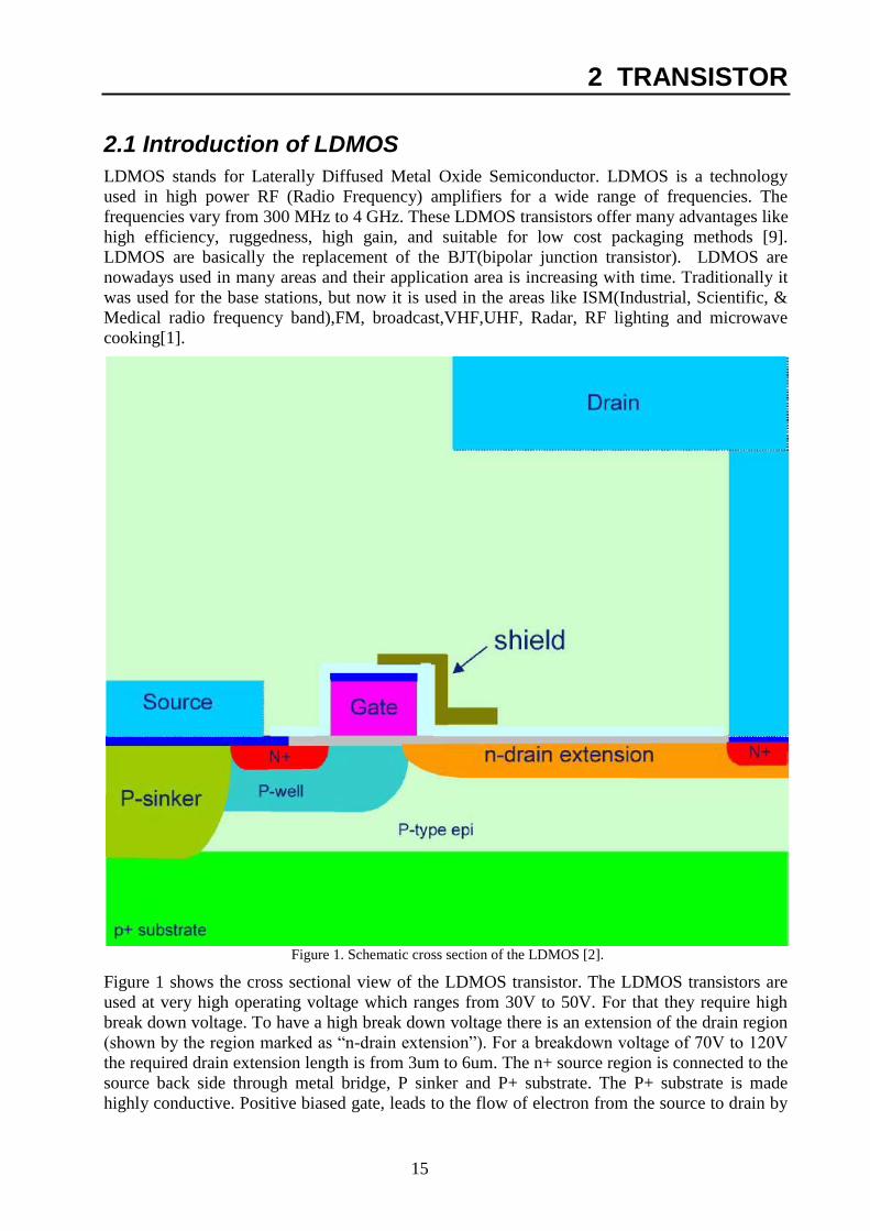
Figure 1. Schematic cross section of the LDMOS [2].
Figure 1 shows the cross sectional view of the LDMOS transistor. The LDMOS transistors are
used at very high operating voltage which ranges from 30V to 50V. For that they require high
break down voltage. To have a high break down voltage there is an extension of the drain region
(shown by the region marked as “n-drain extension”). For a breakdown voltage of 70V to 120V
the required drain extension length is from 3um to 6um. The n+ source region is connected to the
source back side through metal bridge, P sinker and P+ substrate. The P+ substrate is made
highly conductive. Positive biased gate, leads to the flow of electron from the source to drain by

16
inverting the laterally diffused p- well channel. The gate is shielded from the drain by a field
plate as shown in figure 1. This will result in low feedback capacitance and hot carrier reliability
properties [1].
To have a high gain and good reliability of LDMOS, the thermal oxide of the gate is made thin at
the source side in comparison to the drain side. Like a CMOS transistor, the gate length is
reducing with time which has resulted in more gain [1]. Present gate length is 250nm.
This thesis work was done on the power application of the LDMOS. In this application many
LDMOS devices are put in parallel in a thin finger shape. These are generally mounted on the
ceramic or plastic package. The drain and gate are connected via bond wires to the leads and the
flange is soldered on the back side of the source. Both the input and output impedance are very
less. They are around 1-2 ohm. External matching network is needed to make the impedance of
50 ohm on both the input and output side of the transistor.
17
2.2 LDMOS Transistor Background
There are over 200 types of different configuration LDMOS available in the market for various
applications. These applications can be broadly classified as
Base stations (Cellular and WiMAX)- The term Base stations includes mobile and
wireless infrastructures. RF transistors plays an important role in these kinds of systems.
WiMax stands for Worldwide Interoperability for Microwave Access, is a
telecommunication technology which is used to provide broadband internet without any
use of cables. Cellular is a mobile technology. The transistor which has been redesigned
has its application under this category.
Broadcast- This section is mainly consisting of FM (frequency Modulation) and
television broadcasting. There are four segments namely FM broadcast, VHF (Very High
Frequency, 30MHz to 300MHz) TV, UHF (Ultra High Frequency, 300 MHz to 3GHz)
and DTV (Digital television) used for High Definition channels.
ISM (Industrial, Scientific and Medical)- Broadly classifed category which uses RF
power for industrial, scientific, medical and domestic purposes excluding
telecommunication. Some of the example area of applications are RF dryer, welding
machines, medical equipments like MRI, RF lighting, oven and in automatic industry.
Microwave and defence/Avionics- This is a very wide category. The defence/Avionics
need the RF transistors for Radar for different bands like S and L, Military and Satellite
Communications, traffic control, weather radar and Electronic Warfare. Here the
frequency range goes to 4GHz and need very high power.Ruggness and durability is
another key factor in this application.
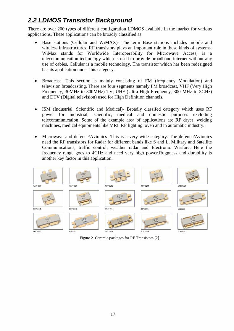
Figure 2. Ceramic packages for RF Transistors [2].
18
According to the technology the RF semiconductors devices can be classified as
Si (Silicon) technology – This technology is the maximun used one. It a good
compromise in terms of cost, RF performance, high –voltage operation and ease to use.
These devices can handle very high power and are able to be used to frequencies over 4
GHz. This is the technology used for the studies presented in this report.
SiC (Silicon Carbide) technology – This technology can be used upto 10GHz of
frequency. It can sustain high operating voltages and have good thermal charactersitics
but has high cost.
GaAs (Gallium Arsenide) technology - This can be used till the frequency of 100GHz.
Now days it is used for 3GHz to 20 GHz applications. This technology is not the first
choice for Basestation applications due to it‟s intrinsic higher cost and difficulty to meet
high voltage operation requirements.
GaN (Galllium Nitride) – It is the most recent technology and have lot of potential. It can
be used for the frequencies upto 50 GHz. The drawback of this technology is the high
cost.
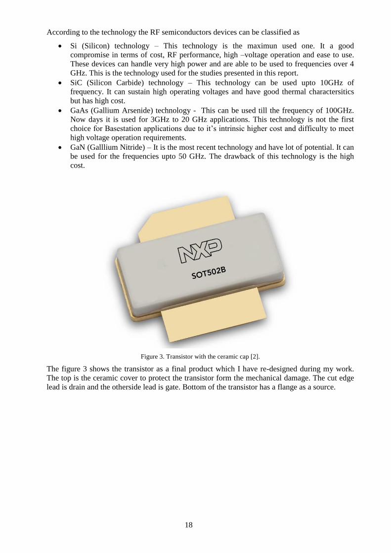
Figure 3. Transistor with the ceramic cap [2].
The figure 3 shows the transistor as a final product which I have re-designed during my work.
The top is the ceramic cover to protect the transistor form the mechanical damage. The cut edge
lead is drain and the otherside lead is gate. Bottom of the transistor has a flange as a source.
19
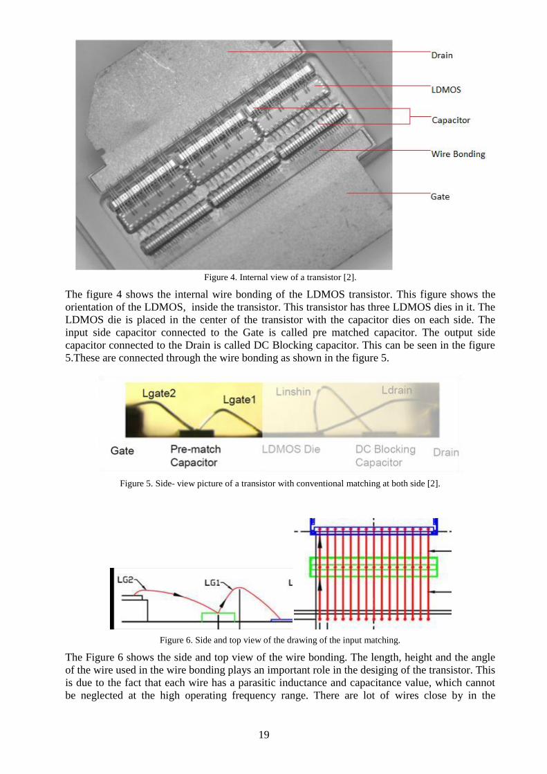
Figure 4. Internal view of a transistor [2].
The figure 4 shows the internal wire bonding of the LDMOS transistor. This figure shows the
orientation of the LDMOS, inside the transistor. This transistor has three LDMOS dies in it. The
LDMOS die is placed in the center of the transistor with the capacitor dies on each side. The
input side capacitor connected to the Gate is called pre matched capacitor. The output side
capacitor connected to the Drain is called DC Blocking capacitor. This can be seen in the figure
5.These are connected through the wire bonding as shown in the figure 5.
Figure 5. Side- view picture of a transistor with conventional matching at both side [2].
Figure 6. Side and top view of the drawing of the input matching.
The Figure 6 shows the side and top view of the wire bonding. The length, height and the angle
of the wire used in the wire bonding plays an important role in the desiging of the transistor. This
is due to the fact that each wire has a parasitic inductance and capacitance value, which cannot
be neglected at the high operating frequency range. There are lot of wires close by in the

20
wirebonding which results in mutual inductance. All these factors causes lot of careful designing
work in the RF transistor. All the individual components in the transistor should have minimum
spacing with each other( which is called as clearing space). The clearing spaces that has to be
taken into the account are the clearance between the each dies, space between the die to the
ringframe of the transistor and the spacing between the the two wires.
Figure 7. Equivalent model of transistor in terms of capacitor and inductance [2].
The figure 7 shows that internal matching and equivalent model of the transistor. The wire
bonding is represented as an inductor. The package and die also contribute to parasitic
inductance. The two capacitances are connected to the LDMOS via inductor. The combination of
the capacitor and inductor forms a resonant frequency both at the input and output side. Hence
the operating frequency of the transistor is constrained by the resonance frequency at both sides.
Various methods are used to increase operating band of frequency which are out of scope of this
report.

21
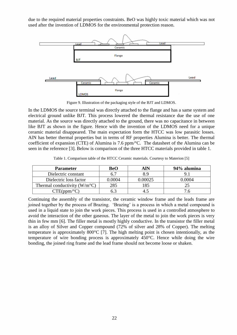
2.3 Packaging Details of Transistor
The RF transistor works at very high frequency and high power. This involves an efficient
packaging of a transistor which works properly at all the working conditions. The packaging of a
transistor consists of a flange, window frame, leads and a ceramic lid as shown in the figure 8.
Figure 8. Illustration of constituent components of a transistor package [2].
The flange is made of a three layers material having Copper Molybdenum in between the Copper
layers. This is also called as CPC (Cu-CuMo-Cu) material. “The lateral structure of the layers is
symmetrical with a thickness ratio of 1:4:1” [4]. This material is very hard, has high thermal
conductivity and a low thermal expansion. More detail about the material properties of flange
can be found in the reference [17]. The flange has a platting of a nickel, copper and gold. The top
surface of the flange where the dies are attached are coated with Nickel Cobalt (ratio of 10% to
20%). This is done to avoid the formation of the compound called Copper silicide, which has a
very high thermal resistance and is brittle. This composition is formed by the interaction of the
Copper from the flange and the Silicon from the dies.
The window frame is made of a ceramic material which is a High Temperature Cofired Ceramic
(HTCC). The HTCC have a high mechanical strength, good thermal conductivity, low expansion
coefficient and suitable for high frequency usages. The HTCC is generally made of Beryllium
Oxide (BeO), aluminum Nitride (AlN) or Alumina (Al2O3). In the old times around 40 years ago
BeO was used for HTCC. In those times BJT was used instead of LDMOS as LDMOS was not
invented at that time. Due to the packaging style of the BJT it was necessary to have a HTCC
with electrical insulator and thermal conductivity as shown in the figure 9. This was due to the
fact that the collector terminal was connected to the flange through a ceramic material. This
added the thermal resistance of the ceramic material along with the flange material. The ceramic
material also added a capacitor from the collector terminal to the ground. Hence the packaging of
the BJT was complicated. The best available option for the ceramic material was BeO for BJT
22
due to the required material properties constraints. BeO was highly toxic material which was not
used after the invention of LDMOS for the environmental protection reason.
Figure 9. Illustration of the packaging style of the BJT and LDMOS.
In the LDMOS the source terminal was directly attached to the flange and has a same system and
electrical ground unlike BJT. This process lowered the thermal resistance due the use of one
material. As the source was directly attached to the ground, there was no capacitance in between
like BJT as shown in the figure. Hence with the invention of the LDMOS need for a unique
ceramic material disappeared. The main expectation form the HTCC was low parasitic losses.
AlN has better thermal properties but in terms of RF properties Alumina is better. The thermal
coefficient of expansion (CTE) of Alumina is 7.6 ppm/°C. The datasheet of the Alumina can be
seen in the reference [3]. Below is comparison of the three HTCC materials provided in table 1.
Table 1. Comparison table of the HTCC Ceramic materials. Courtesy to Materion [5]
Parameter BeO AlN 94% alumina
Dielectric constant 6.7 8.9 9.1
Dielectric loss factor 0.0004 0.00025 0.0004
Thermal conductivity (W/m°C) 285 185 25
CTE(ppm/°C) 6.3 4.5 7.6
Continuing the assembly of the transistor, the ceramic window frame and the leads frame are
joined together by the process of Brazing. „Brazing‟ is a process in which a metal compound is
used in a liquid state to join the work pieces. This process is used in a controlled atmosphere to
avoid the interaction of the other gaseous. The layer of the metal to join the work pieces is very
thin in few mm [6]. The filler metal is mostly highly conductive. In the transistor the filler metal
is an alloy of Silver and Copper compound (72% of silver and 28% of Copper). The melting
temperature is approximately 800°C [7]. The high melting point is chosen intentionally, as the
temperature of wire bonding process is approximately 450°C. Hence while doing the wire
bonding, the joined ring frame and the lead frame should not become loose or shaken.
23
Table 2. Material Properties of Silver Copper Brazing material. Courtesy [7]
Composition Ag(72%),Cu(28%)
Melting Point 1435°F(780°C)
Flow Point 1435°F(780°C)
Brazing Temp 1650°F(900°C)
Color When Brazed White
Density 5.275 Tr. Oz./Cu.In (lb./Cu.In.)
Specific Gravity 10.009
The lead frames are made of Kovar. Kovar is an alloy of Iron, Nickel and cobalt. The alloy has a
high mechanical strength which makes is suitable for the wire bonding. The wire bonding
process requires a hard plane which does not shake or a have a spongy effect. In the absence of
which, the wires will be shaken and they will not be placed properly at a correct angle. The
Kovar has a very low coefficient of thermal expansion which is a closed value to that of Alumina
ceramic, which makes it best for this application. The Kovar has uniform physical and
mechanical properties even after making it in thin sheet which is very suitable for the given
application. The transistor has to be soldered on the application system through the lead frames,
which also requires good solder able properties. The Kovar has a very high melting point of
approximately 1450°C which makes the wire bonding convenient at 450°C.
Table 3. Material properties of Kovar. Courtesy [8]
Specific gravity 8.36
Density 8359 kg/cu m
Thermal conductivity 17.3 W/m-K
Electrical resistivity 490 microhm-mm
Modulus of elasticity 138 MPa x 10(3)
Melting Point 1450°C
More details about the Kovar properties can be seen in the references [8] [14]. The lead frame is
platted with Nickel-Gold to have better thermal conductivity. It has a few strikes of Nickel
followed by a gold platting of 50 micrometer thickness. The wire bonding is done with an
Aluminum wire with 50micrometer. The active die (LDMOS) which is placed on the flange is
made up of silicon wafer and it is Gold platted at the bottom for better thermal conduction. The
capacitors which are placed along the side of the active die are also gold platted from the bottom
where they are placed on the flange. The epoxy glue is used to attach the ceramic ring frame to
the flange and to attach the cover lid to the transistor.
The packaging process which has been explained above has lot of steps which make the whole
packaging process more complex and costly. The new novel transistor designed during this
thesis work has lesser packaging steps and is very cost efficient. The work done in this project is
to find out a solution to replace the lead frame with a suitable PCB material which will reduce
the effective cost but will give the same performance. The basic idea is to have the transistors
with three constituents in packaging. These steps will be of flange, PCB leads and the protective
lead.
24
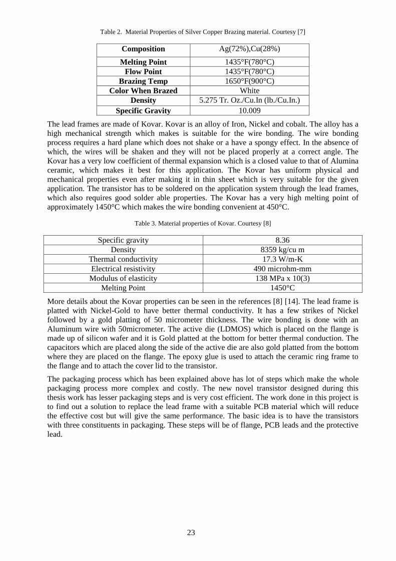
2.4 BLF7G20LS-200 Description
BLF7G20L(S)-200 is a currently available product of NXP Semiconductors. The particular
transistor can provide maximum of 200 watts output power with the operating frequencies
between 1805MHz to 1990MHz. It is used for base station applications. The work done during
this thesis work involved redesign of the package of this transistor. The figure 10 shows the
transistor name description.
Figure 10. Description of the product name[2].
This transistor needs a Vds (Drain to source voltage) of 28V and has an efficiency of 33%. It has
various qualities like low Rth (thermal resistance) which results in better thermal stability. It has
low memory effect and low output capacitance for better operation. It has also a broadband
operational frequency.
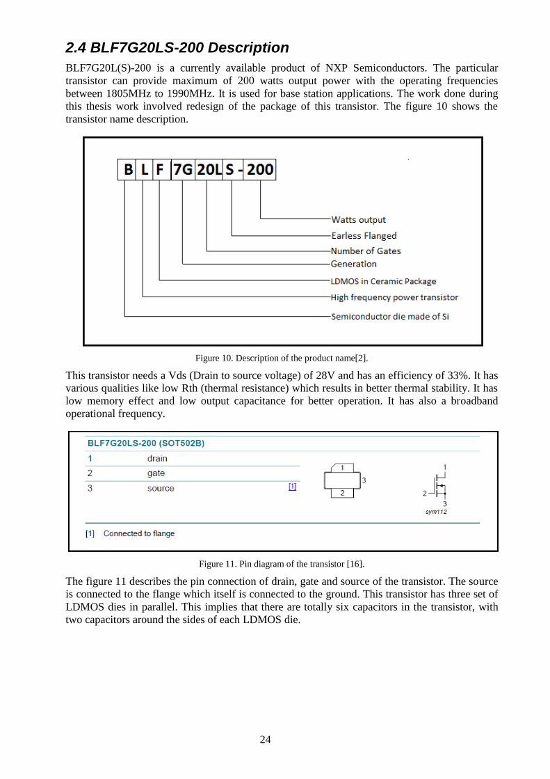
Figure 11. Pin diagram of the transistor [16].
The figure 11 describes the pin connection of drain, gate and source of the transistor. The source
is connected to the flange which itself is connected to the ground. This transistor has three set of
LDMOS dies in parallel. This implies that there are totally six capacitors in the transistor, with
two capacitors around the sides of each LDMOS die.
25
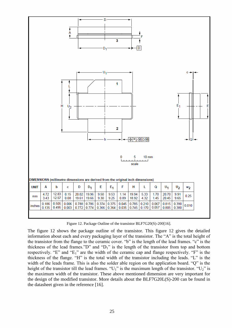
Figure 12. Package Outline of the transistor BLF7G20(S)-200[16].
The figure 12 shows the package outline of the transistor. This figure 12 gives the detailed
information about each and every packaging layer of the transistor. The “A” is the total height of
the transistor from the flange to the ceramic cover. “b” is the length of the lead frames. “c” is the
thickness of the lead frames.”D” and “D1” is the length of the transistor from top and bottom
respectively. “E” and “E1” are the width of the ceramic cap and flange respectively. “F” is the
thickness of the flange. “H” is the total width of the transistor including the leads. “L” is the
width of the leads frame. This is also the solder able region on the application board. “Q” is the
height of the transistor till the lead frames. “U1” is the maximum length of the transistor. “U2” is
the maximum width of the transistor. These above mentioned dimension are very important for
the design of the modified transistor. More details about the BLF7G20L(S)-200 can be found in
the datasheet given in the reference [16].
26
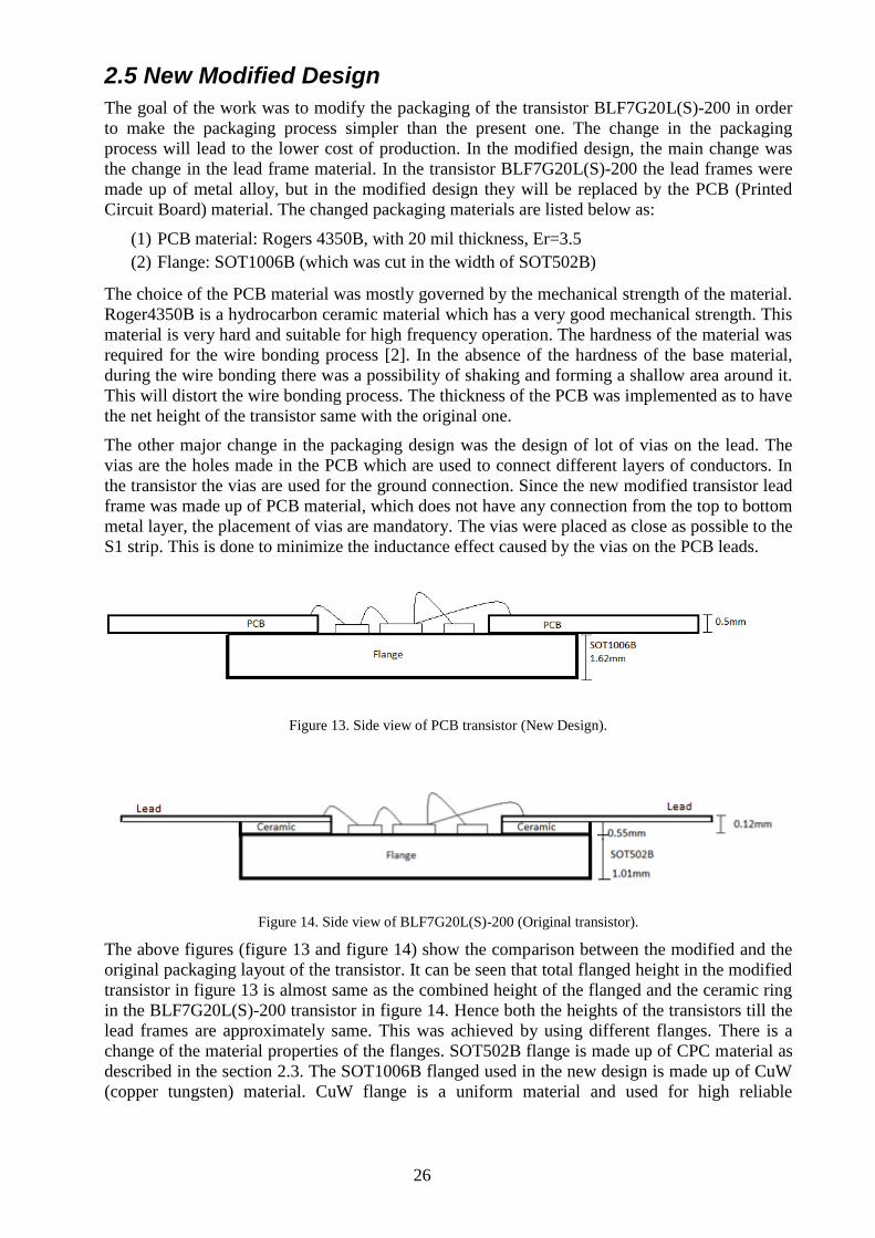
2.5 New Modified Design
The goal of the work was to modify the packaging of the transistor BLF7G20L(S)-200 in order
to make the packaging process simpler than the present one. The change in the packaging
process will lead to the lower cost of production. In the modified design, the main change was
the change in the lead frame material. In the transistor BLF7G20L(S)-200 the lead frames were
made up of metal alloy, but in the modified design they will be replaced by the PCB (Printed
Circuit Board) material. The changed packaging materials are listed below as:
(1) PCB material: Rogers 4350B, with 20 mil thickness, Er=3.5
(2) Flange: SOT1006B (which was cut in the width of SOT502B)
The choice of the PCB material was mostly governed by the mechanical strength of the material.
Roger4350B is a hydrocarbon ceramic material which has a very good mechanical strength. This
material is very hard and suitable for high frequency operation. The hardness of the material was
required for the wire bonding process [2]. In the absence of the hardness of the base material,
during the wire bonding there was a possibility of shaking and forming a shallow area around it.
This will distort the wire bonding process. The thickness of the PCB was implemented as to have
the net height of the transistor same with the original one.
The other major change in the packaging design was the design of lot of vias on the lead. The
vias are the holes made in the PCB which are used to connect different layers of conductors. In
the transistor the vias are used for the ground connection. Since the new modified transistor lead
frame was made up of PCB material, which does not have any connection from the top to bottom
metal layer, the placement of vias are mandatory. The vias were placed as close as possible to the
S1 strip. This is done to minimize the inductance effect caused by the vias on the PCB leads.
Figure 13. Side view of PCB transistor (New Design).
Figure 14. Side view of BLF7G20L(S)-200 (Original transistor).
The above figures (figure 13 and figure 14) show the comparison between the modified and the
original packaging layout of the transistor. It can be seen that total flanged height in the modified
transistor in figure 13 is almost same as the combined height of the flanged and the ceramic ring
in the BLF7G20L(S)-200 transistor in figure 14. Hence both the heights of the transistors till the
lead frames are approximately same. This was achieved by using different flanges. There is a
change of the material properties of the flanges. SOT502B flange is made up of CPC material as
described in the section 2.3. The SOT1006B flanged used in the new design is made up of CuW
(copper tungsten) material. CuW flange is a uniform material and used for high reliable
27
applications [27]. There was a minute variation in the height of the modified transistor which
was acceptable and does not affect in its normal operation.
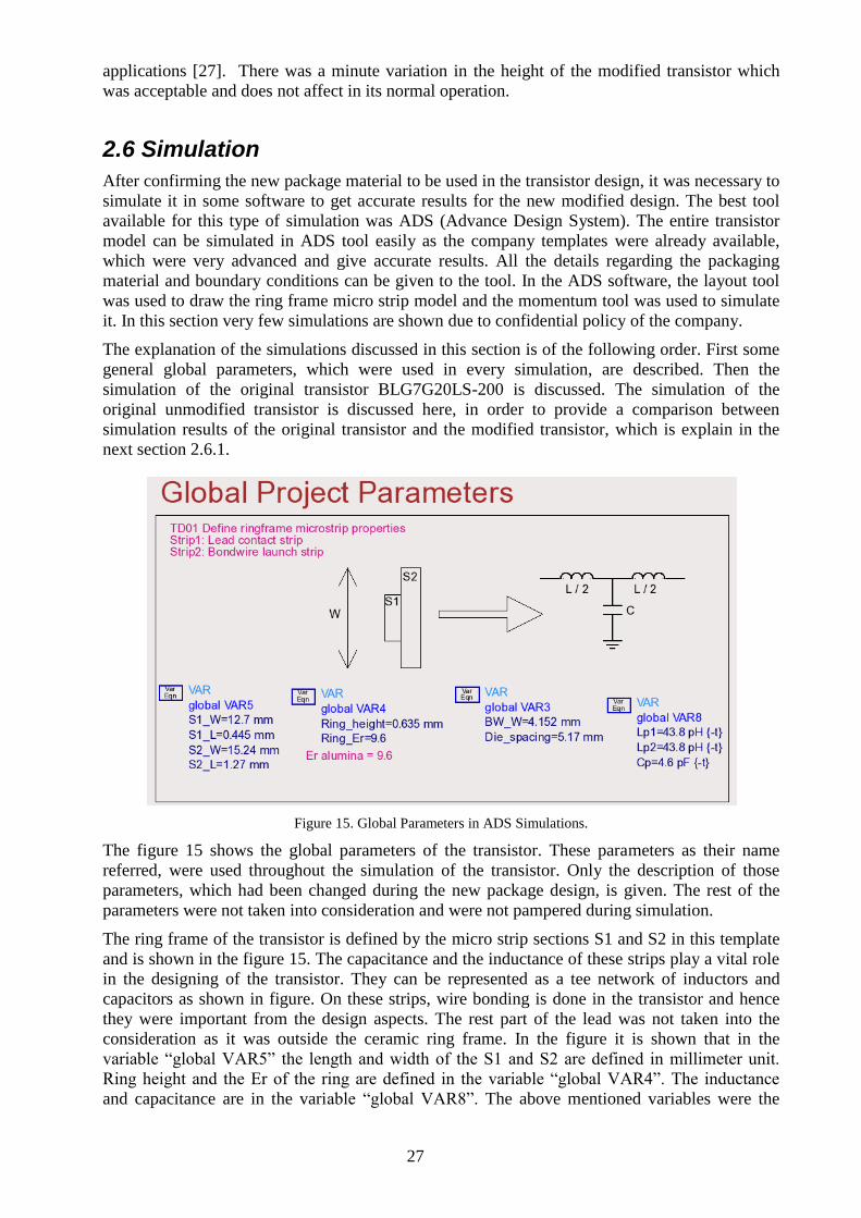
2.6 Simulation
After confirming the new package material to be used in the transistor design, it was necessary to
simulate it in some software to get accurate results for the new modified design. The best tool
available for this type of simulation was ADS (Advance Design System). The entire transistor
model can be simulated in ADS tool easily as the company templates were already available,
which were very advanced and give accurate results. All the details regarding the packaging
material and boundary conditions can be given to the tool. In the ADS software, the layout tool
was used to draw the ring frame micro strip model and the momentum tool was used to simulate
it. In this section very few simulations are shown due to confidential policy of the company.
The explanation of the simulations discussed in this section is of the following order. First some
general global parameters, which were used in every simulation, are described. Then the
simulation of the original transistor BLG7G20LS-200 is discussed. The simulation of the
original unmodified transistor is discussed here, in order to provide a comparison between
simulation results of the original transistor and the modified transistor, which is explain in the
next section 2.6.1.
Figure 15. Global Parameters in ADS Simulations.
The figure 15 shows the global parameters of the transistor. These parameters as their name
referred, were used throughout the simulation of the transistor. Only the description of those
parameters, which had been changed during the new package design, is given. The rest of the
parameters were not taken into consideration and were not pampered during simulation.
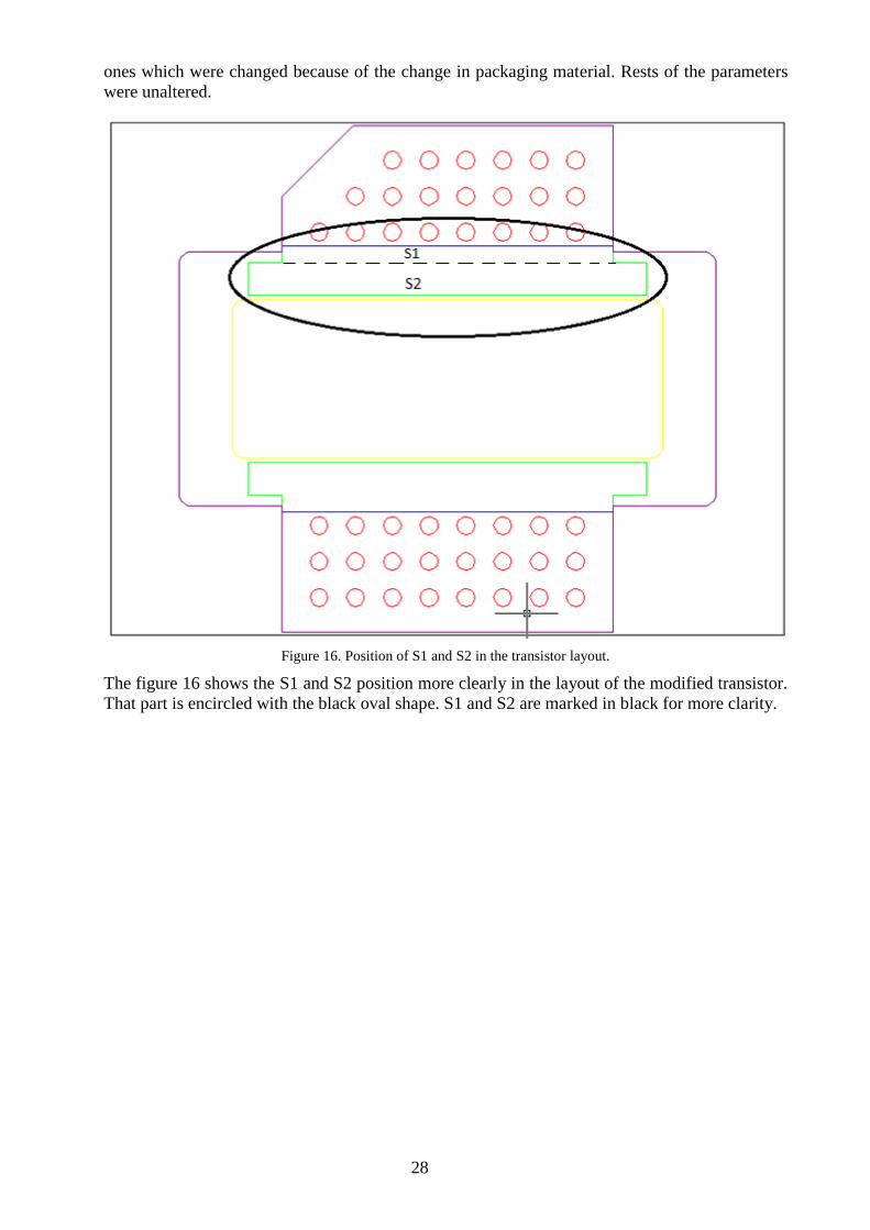
The ring frame of the transistor is defined by the micro strip sections S1 and S2 in this template
and is shown in the figure 15. The capacitance and the inductance of these strips play a vital role
in the designing of the transistor. They can be represented as a tee network of inductors and
capacitors as shown in figure. On these strips, wire bonding is done in the transistor and hence
they were important from the design aspects. The rest part of the lead was not taken into the
consideration as it was outside the ceramic ring frame. In the figure it is shown that in the
variable “global VAR5” the length and width of the S1 and S2 are defined in millimeter unit.
Ring height and the Er of the ring are defined in the variable “global VAR4”. The inductance
and capacitance are in the variable “global VAR8”. The above mentioned variables were the
28
ones which were changed because of the change in packaging material. Rests of the parameters
were unaltered.
Figure 16. Position of S1 and S2 in the transistor layout.
The figure 16 shows the S1 and S2 position more clearly in the layout of the modified transistor.
That part is encircled with the black oval shape. S1 and S2 are marked in black for more clarity.
29
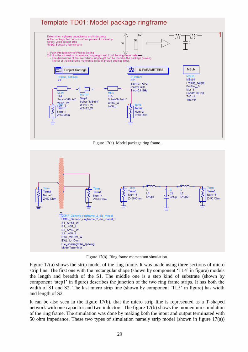
Figure 17(a). Model package ring frame.
Figure 17(b). Ring frame momentum simulation.
Figure 17(a) shows the strip model of the ring frame. It was made using three sections of micro
strip line. The first one with the rectangular shape (shown by component „TL4‟ in figure) models
the length and breadth of the S1. The middle one is a step kind of substrate (shown by
component „step1‟ in figure) describes the junction of the two ring frame strips. It has both the
width of S1 and S2. The last micro strip line (shown by component „TL5‟ in figure) has width
and length of S2.
It can be also seen in the figure 17(b), that the micro strip line is represented as a T-shaped
network with one capacitor and two inductors. The figure 17(b) shows the momentum simulation
of the ring frame. The simulation was done by making both the input and output terminated with
50 ohm impedance. These two types of simulation namely strip model (shown in figure 17(a))
30
and momentum (shown in figure 17(b)) were done to get better results. By comparing their
simulation results, one can get very accurate results. The momentum simulations were
considered more accurate than the strip model.
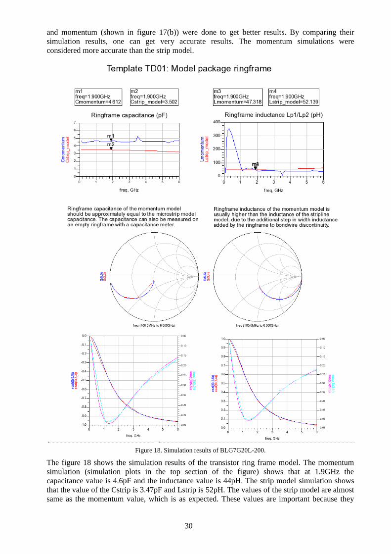
Figure 18. Simulation results of BLG7G20L-200.
The figure 18 shows the simulation results of the transistor ring frame model. The momentum
simulation (simulation plots in the top section of the figure) shows that at 1.9GHz the
capacitance value is 4.6pF and the inductance value is 44pH. The strip model simulation shows
that the value of the Cstrip is 3.47pF and Lstrip is 52pH. The values of the strip model are almost
same as the momentum value, which is as expected. These values are important because they

31
depend upon the material which is going to be changed in the new design. The formula used for
the strip and momentum model is described by the equations (1), (2), (3) and (4). The
impedances used in the equations corresponds to the impedance of the various nodes shown in
the figure 17. In these equations Z12 corresponds to impedance from term2 to term1 as shown in
the figure 17(a). The “im” in the equations corresponds to the imaginary function.
( ) (
( )
)
( )
( ) (
( )
)
( )
(
( )
)
( )
(
( )
)
( )
In the smith chart plots in figure 18 corresponding to the S parameter of S(5, 5) and S(3, 3)
shows the return loss from the frequency 100MHz to 6GHz. These S parameters are called as
scattering parameters.
S(5, 6) and S(3, 4) represents the insertion loss. Ideally return loss should be close to infinity and
the insertion loss should be close to zero value. Please refer [25] for more information on the
calculation of the return and insertion loss. The same parameters are shown in the graph in
bottom of figure 18 by separating the real and imaginary part of the impedance. These charts
provide more detailed view of the values at each frequency. These graphs will be considered as
reference graphs for the comparison of the simulation results of the modified transistor.

32
2.6.1 Modified Ring Frame Simulation
Figure 19. Simulation of the modified transistor.
The simulation setup shown in figure 19 was done by modifying the momentum file in the
Momentum ADS. This momentum file of ring frame layout is shown in the figure 20. This
momentum file was simulated and it was attached using the „SNP1‟ component as shown in the
figure 19.
Figure 20. Momentum layout of the PCB micro strip line
The figure 20 shows the layout of the micro strip line which was a part used to make the ring
frame. Both the pictures are same with the difference of the background color. They are provided
for the better understanding of the layout. Four ports were connected to the micro strip line
(shown by P1, P2, P3 and P4) for making the connection in the circuit. The dimension in this
layout was same as that of the actual strip line of the original transistor.

33
The material was changed from the ceramic to the PCB material. The type of material and metal
thickness were changed and it was simulated with the RF mode enabled. The results from the
simulation setup shown in figure 19 will be compared with the original strip model results shown
in figure 18.
Figure 21. Simulation Results of the PCB transistor.
The capacitance was decreased from 4.6pF value to 1.5pF and the inductance from 52pH to
37pH as shown by the upper plot in figure 21. These values have reduced due to the reduced
value of the Relative permittivity of the material used from 9.6 to 3.5Er. The smith chart plots do
34
not have much variation from the previous simulation in figure 18. Both the return loss and
insertion loss have increased from the previous simulation as shown in the figure 21. In the linear
graphs at the bottom of figure 21, the return loss S(3,3) and insertion loss S(3,4) had become
worse in comparison to the other parameters. The value has shifted to -0.5 and 0.4 respectively
which is relatively high. Since other values have not changed remarkably, changes in design
parameters due to the new lead frame material are in acceptable range. This change can be
compensated while designing for the wire bonding and capacitance in the transistor later.
Thus the change of packaging material of the transistor by the PCB material is acceptable.
2.7 Manufacturing Process
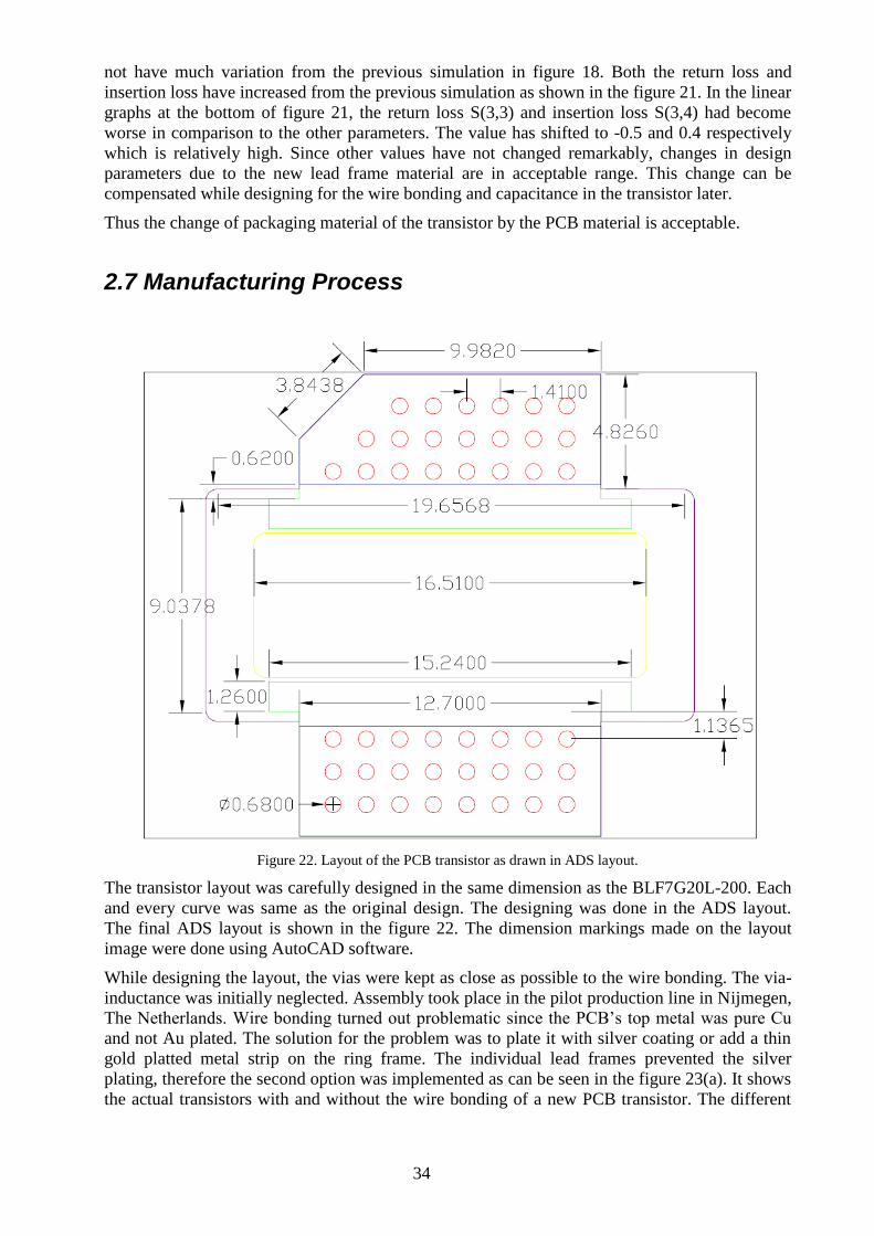
Figure 22. Layout of the PCB transistor as drawn in ADS layout.
The transistor layout was carefully designed in the same dimension as the BLF7G20L-200. Each
and every curve was same as the original design. The designing was done in the ADS layout.
The final ADS layout is shown in the figure 22. The dimension markings made on the layout
image were done using AutoCAD software.
While designing the layout, the vias were kept as close as possible to the wire bonding. The via-
inductance was initially neglected. Assembly took place in the pilot production line in Nijmegen,
The Netherlands. Wire bonding turned out problematic since the PCB‟s top metal was pure Cu
and not Au plated. The solution for the problem was to plate it with silver coating or add a thin
gold platted metal strip on the ring frame. The individual lead frames prevented the silver
plating, therefore the second option was implemented as can be seen in the figure 23(a). It shows
the actual transistors with and without the wire bonding of a new PCB transistor. The different
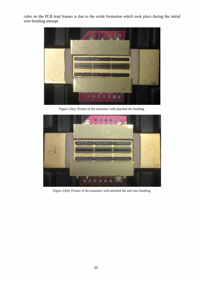
35
color on the PCB lead frames is due to the oxide formation which took place during the initial
wire bonding attempt.
Figure 23(a). Picture of the transistor with attached die bonding.
Figure 23(b). Picture of the transistor with attached die and wire bonding.
36
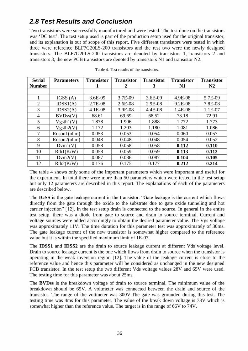
2.8 Test Results and Conclusion
Two transistors were successfully manufactured and were tested. The test done on the transistors
was „DC test‟. The test setup used is part of the production setup used for the original transistor,
and its explanation is out of scope of this report. Five different transistors were tested in which
three were reference BLF7G20LS-200 transistors and the rest two were the newly designed
transistors. The BLF7G20LS-200 transistors are denoted by transistors 1, transistors 2 and
transistors 3, the new PCB transistors are denoted by transistors N1 and transistor N2.
Table 4. Test results of the transistors.
Serial
Number
Parameters Transistor
1
Transistor
2
Transistor
3
Transistor
N1
Transistor
N2
1 IGSS (A) 3.6E-09 3.7E-09 3.6E-09 4.9E-08 5.7E-09
2 IDSS1(A) 2.7E-08 2.6E-08 2.9E-08 9.2E-08 7.8E-08
3 IDSS2(A) 4.1E-08 3.9E-08 4.4E-08 1.4E-08 1.1E-07
4 BVDss(V) 68.61 69.69 68.52 73.18 72.91
5 Vgsth1(V) 1.878 1.906 1.888 1.772 1.773
6 Vgsth2(V) 1.172 1.203 1.180 1.081 1.086
7 Rdson1(ohm) 0.053 0.053 0.054 0.060 0.057
8 Rdson2(ohm) 0.048 0.048 0.048 0.054 0.052
9 Dvm1(V) 0.058 0.058 0.058 0.112 0.110
10 Rth1(K/W) 0.058 0.059 0.059 0.113 0.112
11 Dvm2(V) 0.087 0.086 0.087 0.104 0.105
12 Rth2(K/W) 0.176 0.175 0.177 0.212 0.214
The table 4 shows only some of the important parameters which were important and useful for
the experiment. In total there were more than 50 parameters which were tested in the test setup
but only 12 parameters are described in this report. The explanations of each of the parameters
are described below.
The IGSS is the gate leakage current in the transistor. “Gate leakage is the current which flows
directly from the gate through the oxide to the substrate due to gate oxide tunneling and hot
carrier injection” [12]. In the test setup drain is connected to the source. In general in the entire
test setup, there was a diode from gate to source and drain to source terminal. Current and
voltage sources were added accordingly to obtain the desired parameter value. The Vgs voltage
was approximately 11V. The time duration for this parameter test was approximately of 30ms.
The gate leakage current of the new transistor is somewhat higher compared to the reference
value but it is within the specified maximum limit of 1E-07.
The IDSS1 and IDSS2 are the drain to source leakage current at different Vds voltage level.
Drain to source leakage current is the one which flows from drain to source when the transistor is
operating in the weak inversion region [12]. The value of the leakage current is close to the
reference value and hence this parameter will be considered as unchanged in the new designed
PCB transistor. In the test setup the two different Vds voltage values 28V and 65V were used.
The testing time for this parameter was about 25ms.
The BVDss is the breakdown voltage of drain to source terminal. The minimum value of the
breakdown should be 65V. A voltmeter was connected between the drain and source of the
transistor. The range of the voltmeter was 300V.The gate was grounded during this test. The
testing time was 4ms for this parameter. The value of the break down voltage is 73V which is
somewhat higher than the reference value. The target is in the range of 66V to 74V.
37
Vgsth1 and Vgsth2 are the threshold voltages measured at different Vgs at a certain drain to
source current (Ids). A voltage source was connected between drain and source. A current source
was connected to the source alone. There was also a voltmeter connected from gate to source.
The range of that voltmeter was 3V. The gate terminal was grounded during this test. The Ids
current increases with the increase in threshold voltage till it reaches the saturation point. The
value of both the new transistor is closed to the reference value and hence this parameter is also
good enough.
Rdson1 and Rdson2 are the resistances measured across the drain to source terminal. A
voltmeter was connected across the drain and source terminal and a given current was passed
through it. With the given voltage and current at a point, resistance could be calculated. The
specified amount of Vgs and current was applied to get the value of Rdson. The value of Rdson
of the new transistors is almost same as the reference value.
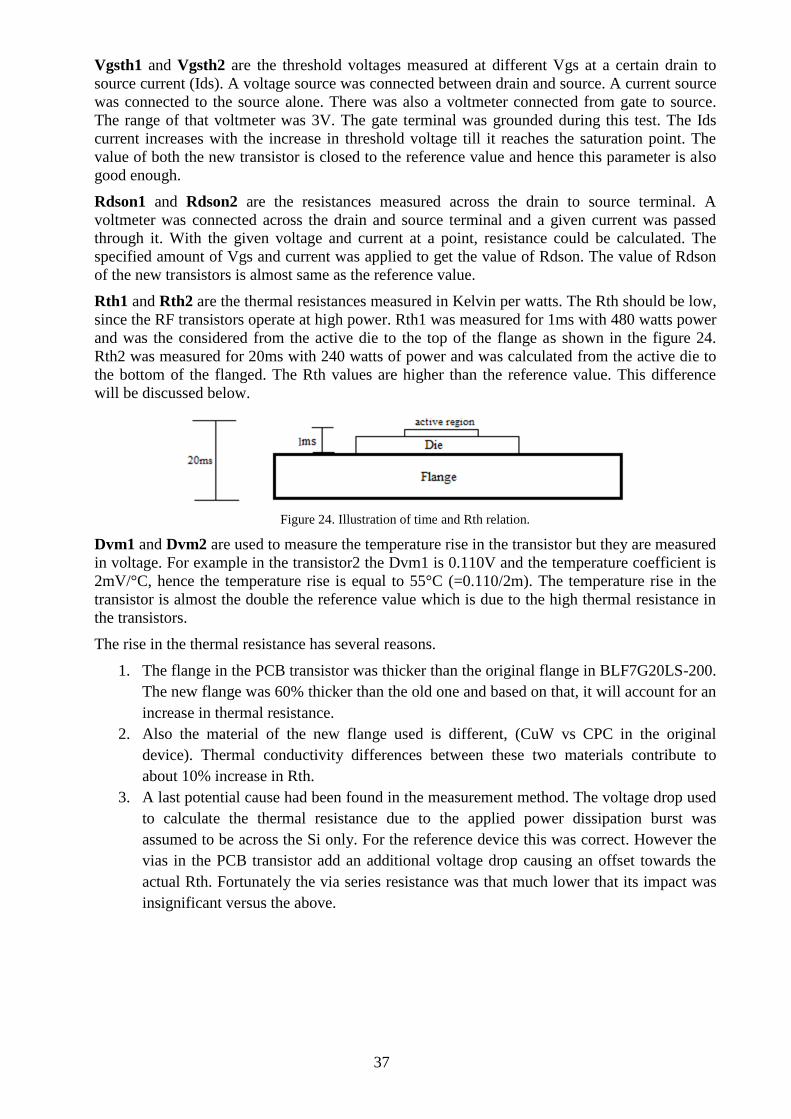
Rth1 and Rth2 are the thermal resistances measured in Kelvin per watts. The Rth should be low,
since the RF transistors operate at high power. Rth1 was measured for 1ms with 480 watts power
and was the considered from the active die to the top of the flange as shown in the figure 24.
Rth2 was measured for 20ms with 240 watts of power and was calculated from the active die to
the bottom of the flanged. The Rth values are higher than the reference value. This difference
will be discussed below.
Figure 24. Illustration of time and Rth relation.
Dvm1 and Dvm2 are used to measure the temperature rise in the transistor but they are measured
in voltage. For example in the transistor2 the Dvm1 is 0.110V and the temperature coefficient is
2mV/°C, hence the temperature rise is equal to 55°C (=0.110/2m). The temperature rise in the
transistor is almost the double the reference value which is due to the high thermal resistance in
the transistors.
The rise in the thermal resistance has several reasons.
1. The flange in the PCB transistor was thicker than the original flange in BLF7G20LS-200.
The new flange was 60% thicker than the old one and based on that, it will account for an
increase in thermal resistance.
2. Also the material of the new flange used is different, (CuW vs CPC in the original
device). Thermal conductivity differences between these two materials contribute to
about 10% increase in Rth.
3. A last potential cause had been found in the measurement method. The voltage drop used
to calculate the thermal resistance due to the applied power dissipation burst was
assumed to be across the Si only. For the reference device this was correct. However the
vias in the PCB transistor add an additional voltage drop causing an offset towards the
actual Rth. Fortunately the via series resistance was that much lower that its impact was
insignificant versus the above.

38
Figure 25. Illustration of vias in the new PCB transistor.
2.9 Future Work
This work was part of the initial feasibility for the research process towards a more cost effective
product / package combination. There is more work to be done in optimizing this design. With
the change in the parasitic capacitance and inductance value, wire bonding and the capacitance
used on the sides of the LDMOS have to be re-optimized.
This work was the first step towards a new concept and can potentially be used in different
applications. One of the applications is described in the next section. It is a microwave amplifier
for radar applications of much higher complexity as the generic transistor presented before.
The work was done by using the standard type of the PCB material available and can be further
investigated with different Er and thickness of the PCB materials. As described in the beginning
of this report, there are varieties of the transistors for various applications.
39
3 MICROWAVE PALLET
3.1 Description of Pallet
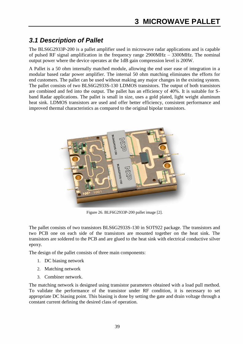
The BLS6G2933P-200 is a pallet amplifier used in microwave radar applications and is capable
of pulsed RF signal amplification in the frequency range 2900MHz – 3300MHz. The nominal
output power where the device operates at the 1dB gain compression level is 200W.
A Pallet is a 50 ohm internally matched module, allowing the end user ease of integration in a
modular based radar power amplifier. The internal 50 ohm matching eliminates the efforts for
end customers. The pallet can be used without making any major changes in the existing system.
The pallet consists of two BLS6G2933S-130 LDMOS transistors. The output of both transistors
are combined and fed into the output. The pallet has an efficiency of 40%. It is suitable for S-
band Radar applications. The pallet is small in size, uses a gold plated, light weight aluminum
heat sink. LDMOS transistors are used and offer better efficiency, consistent performance and
improved thermal characteristics as compared to the original bipolar transistors.
Figure 26. BLF6G2933P-200 pallet image [2].
The pallet consists of two transistors BLS6G2933S-130 in SOT922 package. The transistors and
two PCB one on each side of the transistors are mounted together on the heat sink. The
transistors are soldered to the PCB and are glued to the heat sink with electrical conductive silver
epoxy.
The design of the pallet consists of three main components:
1. DC biasing network
2. Matching network
3. Combiner network.
The matching network is designed using transistor parameters obtained with a load pull method.
To validate the performance of the transistor under RF condition, it is necessary to set
appropriate DC biasing point. This biasing is done by setting the gate and drain voltage through a
constant current defining the desired class of operation.

40
The combiner network combines the output power from both transistors. They should be
balanced properly, it is done with such kind of matching that that if one transistor fails the other
will not fail and can take the entire load. To avoid expensive SMD combiners, this is done by
proper micro strip lines.
Figure 27. Packaging layout dimension [24].
Figure 27 shows the package outline of the pallet. The pallet has the cross section of 3.6cm x
5cm. The place for soldering the transistor is at the center of the pallet. There are four big vias
holes used for the proper alignment of the pallet on the system. The side indents, made on each
side of the pallet, are for screwing it on the system. The PCB thickness is 0.64mm with gold
plated metal layers on top and bottom, heat sink thickness is 0.5cm.
The figure 28 also shows the pads on top of the PCB board. During testing when the pallet is in a
test socket, it is not possible to connect these to the aluminum carrier, as the product is inserted
upside down into the test socket. Therefore extra pads are designed on top of the board to
provide grounding contacts to the test socket. These pads are contacted with metalized vias in the
PCB to the aluminum carrier and are only for testing purposes.
The following figure 28 shows these ground pads placement in the pallet‟s PCB.
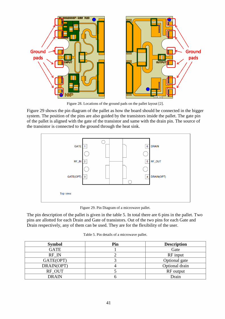
41
Figure 28. Locations of the ground pads on the pallet layout [2].
Figure 29 shows the pin diagram of the pallet as how the board should be connected in the bigger
system. The position of the pins are also guided by the transistors inside the pallet. The gate pin
of the pallet is aligned with the gate of the transistor and same with the drain pin. The source of
the transistor is connected to the ground through the heat sink.
Figure 29. Pin Diagram of a microwave pallet.
The pin description of the pallet is given in the table 5. In total there are 6 pins in the pallet. Two
pins are allotted for each Drain and Gate of transistors. Out of the two pins for each Gate and
Drain respectively, any of them can be used. They are for the flexibility of the user.
Table 5. Pin details of a microwave pallet.
Symbol Pin Description
GATE 1 Gate
RF_IN 2 RF input
GATE(OPT) 3 Optional gate
DRAIN(OPT) 4 Optional drain
RF_OUT 5 RF output
DRAIN 6 Drain

42
3.2 New Design
The old pallet design which has been described above consists of separate parts like two
transistors, two PCB pieces (each for input and output sides of the pallet), and a heat sink. The
transistors were soldered on top of the PCB and were attached to the heat sink. In the new design
which is discussed in this report, the transistors were co-designed together with the PCB and heat
sink parts of the product. The PCB was also consisting of one piece instead of two as before.
This new design is very effective from the point of cost and design. The application
methodology of the transistor made with PCB leads (described in chapter 2) had been
incorporated in this design. The leads are part of the pallet‟s PCB and the PCB leads were
extended to form a full board of pallet. Since the transistors are built into the pallet‟s PCB, the
flange on which the Si chips are attached, need to be incorporated in the total design. The main
work involved here was to redesigning the packaging of the transistor.
3.2.1 Design Approach
The complete layout shown in the figure 30d was designed during the thesis work. It was done
with the ADS layout tool. The modified layout was designed by using the layout of the original
pallet (shown in the figure 28) as reference.
The very first step was to design the outer layout of the transistor BLS6G2933S-130 as
done in the section 2.7. Since this transistor was completely different, the entire transistor
was designed from scratch. The dimensions of the transistor BLS6G2933S-130 were
calculated using the Auto Cad tool. Every dimension is very critical and minute details
have to be taken into consideration like the radius of the corners and the distance of the
lead frame from the center. Dimension precision up to 3 places after the decimal points
were taken into consideration while designing the layout. In the figure 30a the transistor
model as drawn in the ADS is shown. The light blue color is the conductor and it
represents the lead frames. The dark blue color is the ring frame of the transistor which
was made up of a non conductor material.
Figure 30a. Layout of the transistor for the pallet.

43
The figure 30b shows the electrical matching network of the pallet. It was fully made up
of the conductive material. This electrical design is same as the original pallet
BLS6G2933P-200.
The figure as shown in the 30a and 30b were merged together to form the figure as
shown in the 30c. This merging was done while taking the dimensions of the original
pallet into consideration. The outer boundry of the pallet should be same as the original
transistor design and the centre spacing should also remain same without any alteration.
The next step involved was on completing the design in the various parts like making via
hole, making the space for the resistors and capacitors. The addtion of the extra capacitor
on all the sides of the pallet was also done in this step. The exact size of the capacitor and
resistor was done using the reference of the original design.
Figure 30b. Layout of the electrical network of the pallet.
The figure 30d is the complete design of the pallet with the solder mask layer. In the final design
in figure 30c and 30d, the back side of the conductor was also drawn which is represented the
pink colour. All the designs are merged together to form a single PCB layout ready for
manufacturers.

44
Figure 30c. Layout of the pallet with the transistor and the electrical design.
Figure 30d. Design layout of a modified pallet.
Continuing the description of the pallet, the figure 30d shows the completed layout of the
modified pallet based only on a single PCB. The centre rectangular space is left for the wire
45
bonding of the transistors. The light blue color section in the figure represents the conductor on
the PCB. The black dots are the vias for the ground connection. The pink color outline is the
back side conductor area on the PCB. The input and output pins are separated from rest of the
ground plane. The dark shaded blue color represents the soldered mask on the PCB. This
soldered mask helps in component placement accuracy and prevents the excessive flow-out of
solder paste. The electrical difference between the original and modified pallet was taken care
by the addition of four capacitors on the drain and gate of both the transistors and will be
explained later in the section 3.4.
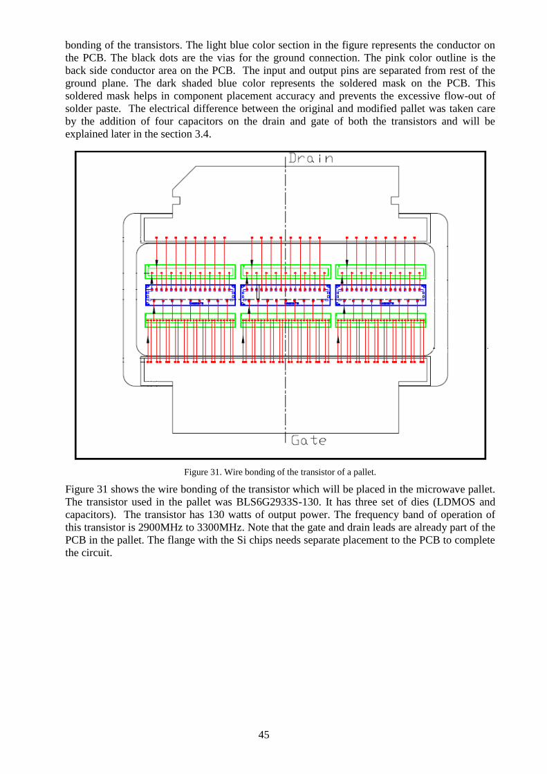
Figure 31. Wire bonding of the transistor of a pallet.
Figure 31 shows the wire bonding of the transistor which will be placed in the microwave pallet.
The transistor used in the pallet was BLS6G2933S-130. It has three set of dies (LDMOS and
capacitors). The transistor has 130 watts of output power. The frequency band of operation of
this transistor is 2900MHz to 3300MHz. Note that the gate and drain leads are already part of the
PCB in the pallet. The flange with the Si chips needs separate placement to the PCB to complete
the circuit.
46
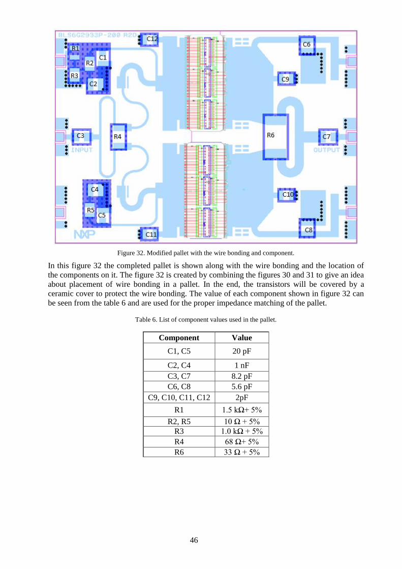
Figure 32. Modified pallet with the wire bonding and component.
In this figure 32 the completed pallet is shown along with the wire bonding and the location of
the components on it. The figure 32 is created by combining the figures 30 and 31 to give an idea
about placement of wire bonding in a pallet. In the end, the transistors will be covered by a
ceramic cover to protect the wire bonding. The value of each component shown in figure 32 can
be seen from the table 6 and are used for the proper impedance matching of the pallet.
Table 6. List of component values used in the pallet.
Component Value
C1, C5 20 pF
C2, C4 1 nF
C3, C7 8.2 pF
C6, C8 5.6 pF
C9, C10, C11, C12 2pF
R1 1.5 kΩ+ 5%
R2, R5 10 Ω + 5%
R3 1.0 kΩ + 5%
R4 68 Ω+ 5%
R6 33 Ω + 5%

47
3.3 Packaging Details
There were lots of changes made in the packaging material of the pallet. The original pallet has
the PCB material of Er (Dielectric material) =6.15, and thickness 0.635mm. The PCB material
used in the original pallet design was „Roger 3006‟ which has low dielectric losses for the high
frequency applications. This PCB material is also suitable for high temperature use. More
details about this PCB material can be obtained from its datasheet in [18]. The original transistor
in the previous generation design were used with lead frames and ceramic package.
The new modified pallet has inbuilt transistors, hence the transistor leads frame was replaced by
traces on the PCB. The original PCB cannot be used as this was too soft for the wire bonding of
the transistor. This reason is already mentioned in previous section. For that reason RO4360 was
used in the new design which is a hydrocarbon ceramic filled material. This PCB is very hard
and has a good mechanical strength for the wire bonding of the transistor. The Er of this material
is 6.15, another important reason for using this particular PCB material. The dielectric constant is
directly proportional to the micro strip line width and altering them implies changing the whole
design. Hence a very careful selection of the PCB material was done in the modified design. The
thickness of the PCB material is 0.61mm. The difference of 0.025mm thickness between the
previous generation design and the new design was considered negligible.
The transistor in the original design had a lead frame and a ceramic ring frame. The dielectric of
a ring frame was Er= 9.6. In the new design the lead frames is created in the PCB material with
Er=6.15. This will cause reduced capacitance of the ring frame and impact the entire design of
the pallet. This is because further matching is done on the basis of the initial value of the
capacitance of the transistor. To compensate this, additional SMD capacitor‟s are added to the
drain and gate of both transistors. This approach is simple and quick in comparison to changing
the whole design. To know the changes in the value of the capacitance, the ring model was
simulated.
48
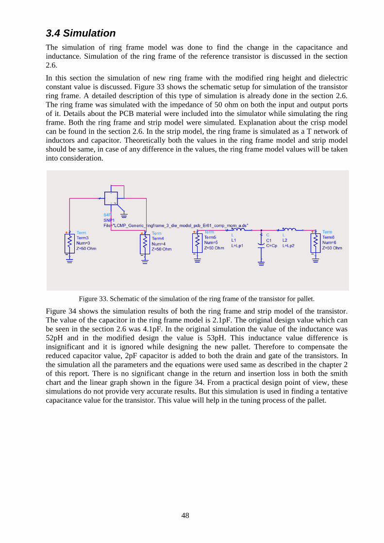
3.4 Simulation
The simulation of ring frame model was done to find the change in the capacitance and
inductance. Simulation of the ring frame of the reference transistor is discussed in the section
2.6.
In this section the simulation of new ring frame with the modified ring height and dielectric
constant value is discussed. Figure 33 shows the schematic setup for simulation of the transistor
ring frame. A detailed description of this type of simulation is already done in the section 2.6.
The ring frame was simulated with the impedance of 50 ohm on both the input and output ports
of it. Details about the PCB material were included into the simulator while simulating the ring
frame. Both the ring frame and strip model were simulated. Explanation about the crisp model
can be found in the section 2.6. In the strip model, the ring frame is simulated as a T network of
inductors and capacitor. Theoretically both the values in the ring frame model and strip model
should be same, in case of any difference in the values, the ring frame model values will be taken
into consideration.
Figure 33. Schematic of the simulation of the ring frame of the transistor for pallet.
Figure 34 shows the simulation results of both the ring frame and strip model of the transistor.
The value of the capacitor in the ring frame model is 2.1pF. The original design value which can
be seen in the section 2.6 was 4.1pF. In the original simulation the value of the inductance was
52pH and in the modified design the value is 53pH. This inductance value difference is
insignificant and it is ignored while designing the new pallet. Therefore to compensate the
reduced capacitor value, 2pF capacitor is added to both the drain and gate of the transistors. In
the simulation all the parameters and the equations were used same as described in the chapter 2
of this report. There is no significant change in the return and insertion loss in both the smith
chart and the linear graph shown in the figure 34. From a practical design point of view, these
simulations do not provide very accurate results. But this simulation is used in finding a tentative
capacitance value for the transistor. This value will help in the tuning process of the pallet.
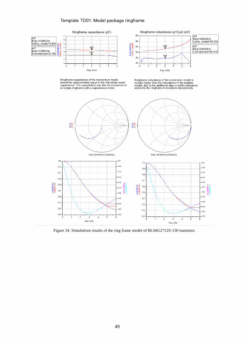
49
Figure 34. Simulations results of the ring frame model of BLS6G2712S-130 transistor.
50
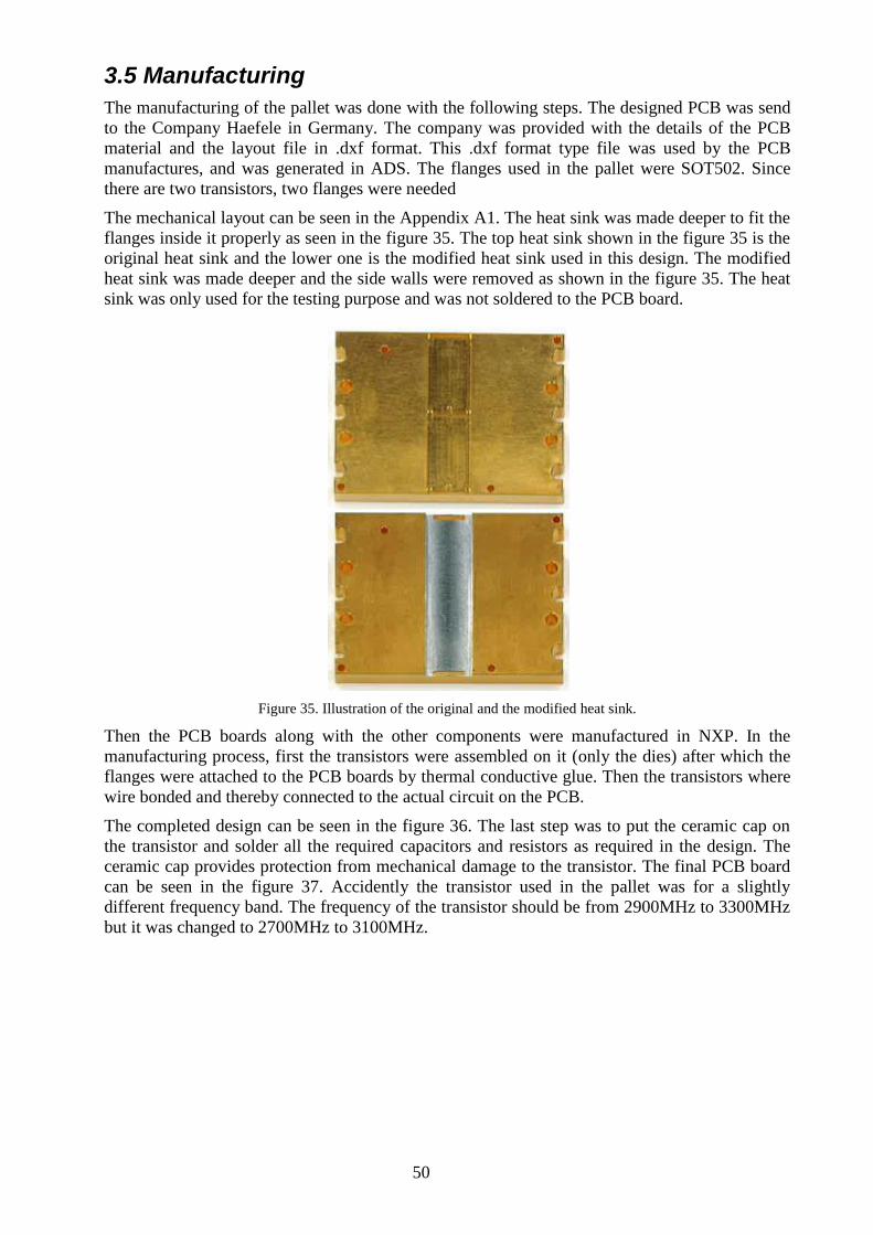
3.5 Manufacturing
The manufacturing of the pallet was done with the following steps. The designed PCB was send
to the Company Haefele in Germany. The company was provided with the details of the PCB
material and the layout file in .dxf format. This .dxf format type file was used by the PCB
manufactures, and was generated in ADS. The flanges used in the pallet were SOT502. Since
there are two transistors, two flanges were needed
The mechanical layout can be seen in the Appendix A1. The heat sink was made deeper to fit the
flanges inside it properly as seen in the figure 35. The top heat sink shown in the figure 35 is the
original heat sink and the lower one is the modified heat sink used in this design. The modified
heat sink was made deeper and the side walls were removed as shown in the figure 35. The heat
sink was only used for the testing purpose and was not soldered to the PCB board.
Figure 35. Illustration of the original and the modified heat sink.
Then the PCB boards along with the other components were manufactured in NXP. In the
manufacturing process, first the transistors were assembled on it (only the dies) after which the
flanges were attached to the PCB boards by thermal conductive glue. Then the transistors where
wire bonded and thereby connected to the actual circuit on the PCB.
The completed design can be seen in the figure 36. The last step was to put the ceramic cap on
the transistor and solder all the required capacitors and resistors as required in the design. The
ceramic cap provides protection from mechanical damage to the transistor. The final PCB board
can be seen in the figure 37. Accidently the transistor used in the pallet was for a slightly
different frequency band. The frequency of the transistor should be from 2900MHz to 3300MHz
but it was changed to 2700MHz to 3100MHz.

51
Figure 36. Image of the designed pallet with the wire bonding.
Figure 37. Image of the top and back side of the designed pallet.

52
3.6 Test Results and Discussion
The four pallets were tested in the test lab. The description of the test setup is very complicated
and is out of scope of this report. The tests were done at different power levels. The main aim of
the test was to find the gain of the pallet with the frequency range and the power level. Four tests
with different power and frequency were done and are discussed individually in the following
sections.
Out of the four pallets, two of them were destroyed while testing after the first test. Hence their
test data is not included in this report. To compare the results with the reference values, one of
the original microwave pallets BLS6G2933P-200 was tested first and given the name as Ref in
all the test results.
3.6.1 Results of Test 1
The Vds (drain to source voltage) of the transistor was set as 32V. The test is done at three
different frequencies from 2900MHz to 3300MHz as shown in the table 7. This is the operational
frequency band of the microwave pallet. Six parameters which were important in respect of the
new design are discussed in each table showing the test results. Two currents Id1 and Id2 are the
drain currents of the transistors from the two drain pins as shown in the figure 29. The RL is the
power dissipated in the load which should be greater than the 6dB. Input (Pin) and output power
(Pout) are expressed in watts. The input power was 20 Watts at all frequency. Gain is calculated
in dB and ideally should be greater than 9.2dB.
The test results with this setup is shown in the table 7.
Table 7. Results of the test1 of the microwave pallet.
Frequency Id1(A) Id2(A) RL(dB) Pin(W) Pout(W) Gain(dB)
2900MHz Ref 6.33319 8.13064 8.34924 19.9673 217.16 10.3646
Pallet 1 3.82576 4.56555 7.67142 19.9464 13.9934 -1.53941
Pallet 2 2.08429 2.33042 7.46203 19.9877 10.4295 -2.82501
3100MHz Ref 8.74134 10.0872 15.0537 19.9115 255.887 11.0895
Pallet 1 6.59159 7.33439 12.1106 19.9158 27.5645 1.41152
Pallet 2 2.58107 2.82794 15.2091 19.9275 11.8283 -2.26529
3300MHz Ref 8.92308 9.91345 14.6619 20.0219 250.499 10.973
Pallet 1 6.85805 7.3886 5.61655 19.9846 37.0873 2.6853
Pallet 2 2.06337 2.24598 6.45975 20.0089 10.0688 -2.98247
The figure 38 shows the graph between the gain and frequency of the reference pallet and the
two new pallets. As seen in the figure the gain of the two pallets is quiet low compared to the
reference value. Pallet2 does not have a positive gain at all and behaves like an attenuator. Rests
of the parameters are also not up to the expected values. This result is not satisfactory at all and
further tests were required.
53
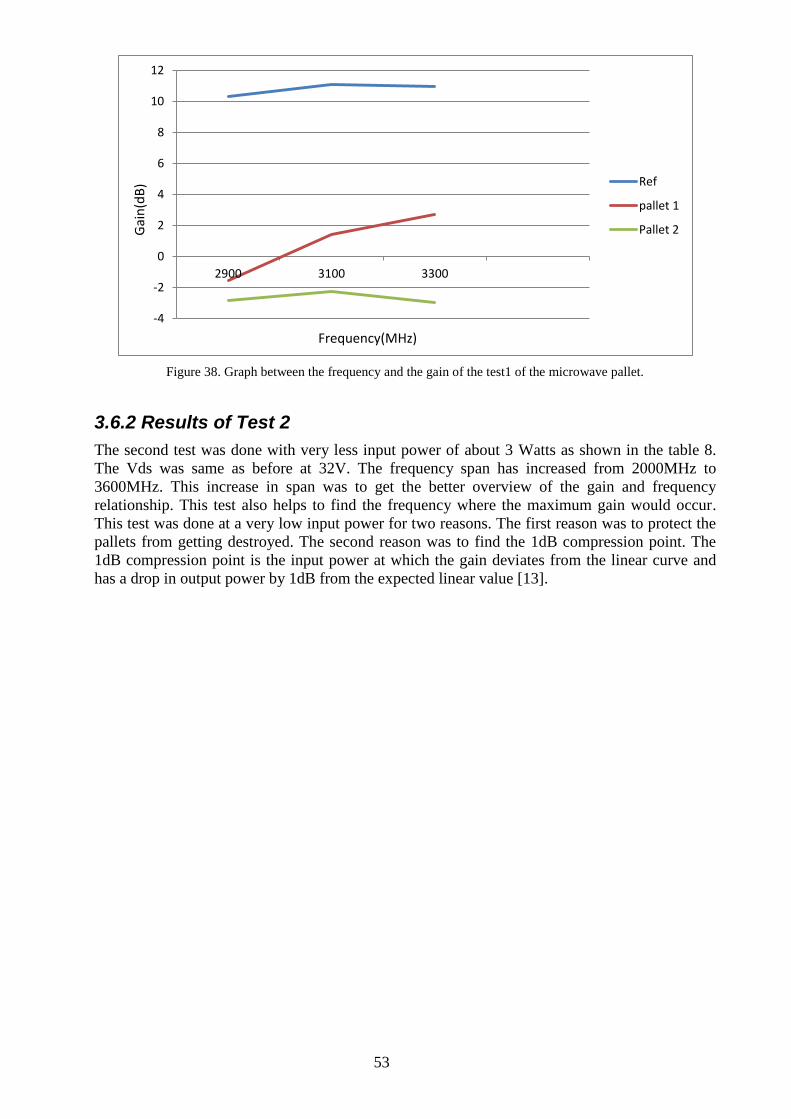
Figure 38. Graph between the frequency and the gain of the test1 of the microwave pallet.
3.6.2 Results of Test 2
The second test was done with very less input power of about 3 Watts as shown in the table 8.
The Vds was same as before at 32V. The frequency span has increased from 2000MHz to
3600MHz. This increase in span was to get the better overview of the gain and frequency
relationship. This test also helps to find the frequency where the maximum gain would occur.
This test was done at a very low input power for two reasons. The first reason was to protect the
pallets from getting destroyed. The second reason was to find the 1dB compression point. The
1dB compression point is the input power at which the gain deviates from the linear curve and
has a drop in output power by 1dB from the expected linear value [13].
-4
-2
0
2
4
6
8
10
12
2900 3100 3300
Ref
pallet 1
Pallet 2
Frequency(MHz)
Gai
n(d
B)

54
Table 8. Results of the test 2 of the microwave pallet.
Frequency Id1(A) Id2(A) RL(dB) Pin(W) Pout(W) Gain(dB)
2000MHz Pallet1 0.640664 0.705589 0.299049 3.01091 0.550602 -7.3786
Pallet 2 0.603314 0.671986 0.286194 3.00073 0.524176 -7.5775
2200MHz Pallet1 2.86228 2.91912 4.83024 3.00019 5.96327 2.98337
Pallet 2 3.24392 3.76872 6.73063 2.9973 9.95111 5.21141
2400MHz Pallet1 0.239857 0.257736 1.23994 3.00782 0.003822 -28.9594
Pallet 2 0.228544 0.256179 1.26641 3.00063 0.003273 -29.6229
2600MHz Pallet1 0.617934 0.663309 0.818514 2.99619 0.014391 0.0351
Pallet 2 0.564505 0.630018 0.836946 2.99631 0.026581 0.069533
2800MHz Pallet1 1.21966 1.30413 3.37736 3.00506 4.34241 1.59878
Pallet 2 1.24 1.37447 3.03686 2.99716 3.02779 0.044165
3000MHz Pallet1 1.88269 2.00947 10.714 2.99702 9.94658 5.20985
Pallet 2 1.78094 1.99691 10.2859 2.99492 8.44982 4.50462
3200MHz Pallet1 2.37301 2.54017 9.74807 2.99783 9.0571 4.80183
Pallet 2 2.27533 2.54077 9.58937 2.99241 8.01039 4.27632
3400MHz Pallet1 1.72448 1.84677 4.74791 2.99312 5.29505 2.47747
Pallet 2 1.69502 1.87825 4.80835 2.99326 4.73114 1.98821
3600MHz Pallet1 0.871863 0.925763 2.75177 2.98746 1.58487 -2.75308
Pallet 2 0.827614 0.901491 2.86636 2.84685 1.27358 -3.49339
Figure 39 shows the graph between the frequency and the gain of the pallets. The maximum gain
reached was 5dB. From 2800MHz to 3400MHz frequency the pallets showed the positive gain.
From the test 2 it was interpreted that this range of frequency from 2800MHz to 3400MHz is a
good band of operation. There was a peak of gain at 2200MHz but at 2400MHZ there was a
great dip in the gain. Hence this frequency region was not taken into the consideration. Another
test was followed with the increase in the input power in the above mentioned frequency band.

55
Figure 39.Graph between the frequency and the gain of the test2 of the microwave pallet.
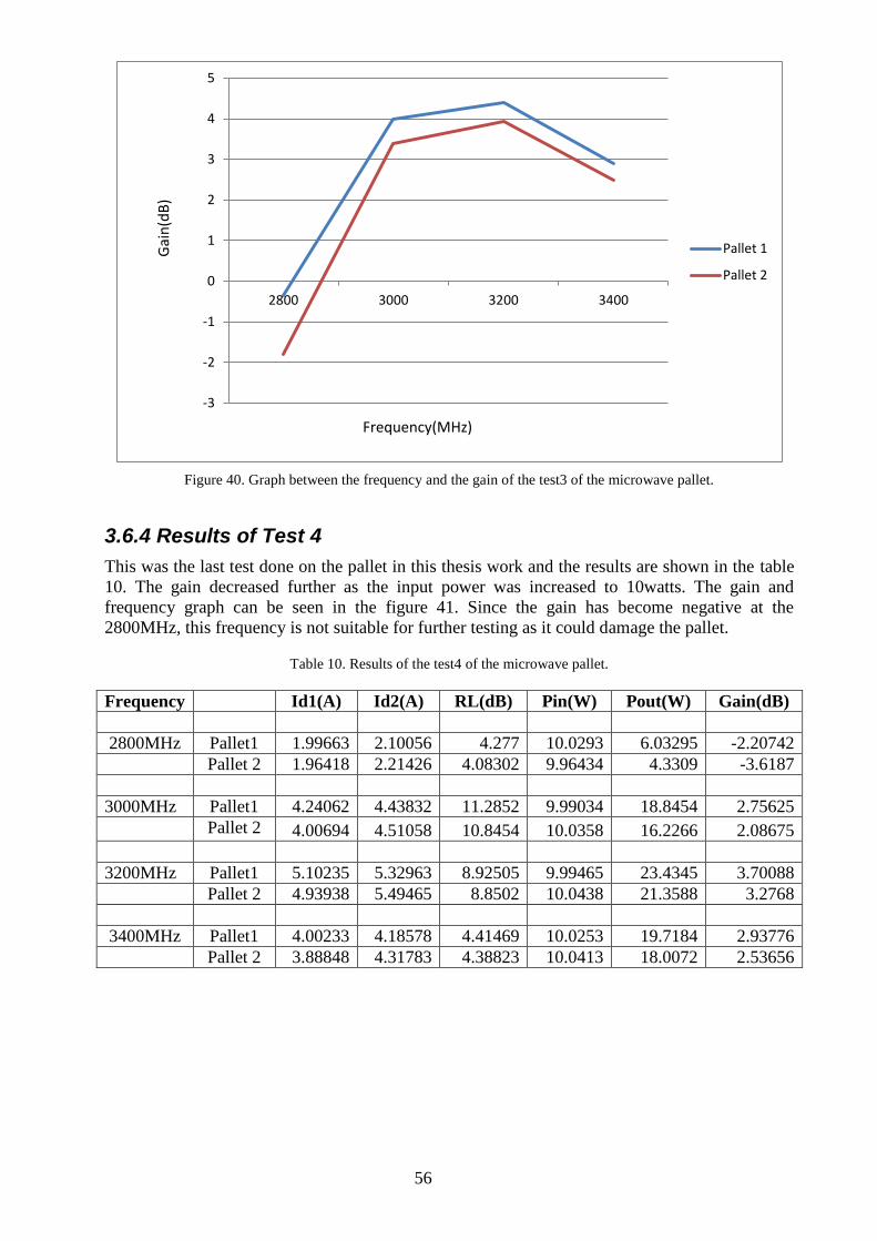
3.6.3 Results of Test 3
The input power was increased to 6 Watts in this test as shown in the table 9. The frequency
range of operation was from 2800MHz to 3400MHz. There was a fall in the gain as the power
has increased as shown in the figure 40. This was due to the fact that 3dB compression point was
already reached and hence there was a decrease in the gain as the input power was increased.
The current and the power dissipation got decreased compared to the reference value.
Table 9.Results of the test 3 of the microwave pallet.
Frequency Id1(A) Id2(A) RL(dB) Pin(W) Pout(W) Gain(dB)
2800MHz Pallet1 1.57314 1.71731 4.16404 5.98638 5.51927 -0.35283
Pallet 2 1.58895 1.80227 3.97194 6.00658 3.96721 -1.80142
3000MHz Pallet1 3.09336 3.36409 10.5332 5.98577 15.183 4.04239
Pallet 2 2.97986 3.36623 10.1804 6.01032 13.0408 3.36406
3200MHz Pallet1 3.77945 4.11045 9.12234 6.01082 16.5746 4.40511
Pallet 2 3.70773 4.12558 9.04129 5.98614 14.852 3.94638
3400MHz Pallet1 2.79742 3.04053 4.6236 5.99122 11.7528 2.92626
Pallet 2 2.76586 3.06616 4.55312 5.97731 10.6523 2.50937
-35
-30
-25
-20
-15
-10
-5
0
5
10
2000 2200 2400 2600 2800 3000 3200 3400 3600
pallet1
pallet2
Frequency(MHz)
Gai
n(d
B)
56
Figure 40. Graph between the frequency and the gain of the test3 of the microwave pallet.
3.6.4 Results of Test 4
This was the last test done on the pallet in this thesis work and the results are shown in the table
10. The gain decreased further as the input power was increased to 10watts. The gain and
frequency graph can be seen in the figure 41. Since the gain has become negative at the
2800MHz, this frequency is not suitable for further testing as it could damage the pallet.
Table 10. Results of the test4 of the microwave pallet.
Frequency Id1(A) Id2(A) RL(dB) Pin(W) Pout(W) Gain(dB)
2800MHz Pallet1 1.99663 2.10056 4.277 10.0293 6.03295 -2.20742
Pallet 2 1.96418 2.21426 4.08302 9.96434 4.3309 -3.6187
3000MHz Pallet1 4.24062 4.43832 11.2852 9.99034 18.8454 2.75625
Pallet 2 4.00694 4.51058 10.8454 10.0358 16.2266 2.08675
3200MHz Pallet1 5.10235 5.32963 8.92505 9.99465 23.4345 3.70088
Pallet 2 4.93938 5.49465 8.8502 10.0438 21.3588 3.2768
3400MHz Pallet1 4.00233 4.18578 4.41469 10.0253 19.7184 2.93776
Pallet 2 3.88848 4.31783 4.38823 10.0413 18.0072 2.53656
-3
-2
-1
0
1
2
3
4
5
2800 3000 3200 3400
Pallet 1
Pallet 2
Frequency(MHz)
Gai
n(d
B)

57
Figure 41. Graph between the frequency and the gain of the test3 of the microwave pallet.
-4
-3
-2
-1
0
1
2
3
4
5
2800 3000 3200 3400
Pallet 1
Pallet 2
Frequency(MHz)
Gai
n(d
B)
58
3.7 Conclusion and future work
The presented test results gave the information that the experiment done in this thesis work on
the microwave pallet was feasible. This analysis was done on the basis of the gain at certain
bandwidth. The maximum gain reached by the pallet was 5dB, which was half the value of the
reference gain in the present microwave pallet BLS6G2933P-200.
This microwave pallet design has not been optimised yet but did prove the feasibility of the
package concept. Following aspects need to be further optimized:
1. The transistor which was built on the pallet was not the correct one. Due to which there
was a difference in operational bandwidth of the pallet and the operational bandwidth of
the transistor built on it. The transistor‟s operational bandwidth was from 2700MHz to
3100MHz and the rest of the pallet bandwidth was from 2900MHz to 3300MHz. This
mismatch between optimized frequency band between transistor and the rest of the
application circuit did cause the gain and actual frequency response to deviate from the
reference design. In the figure 39 there is a dip in gain of about -28dB at a frequency
2400MHz with a bandwidth of 200MHz, which could be due some parasitic resonances
either of the pallet or the transistor.
2. Secondly, the transistors used in the design were also newly designed as mentioned in
the first section of this report. They are not optimised in terms of the wire bonding to
compensate the changes due to different packaging. The RF transistors are very
complicated as they have to take each and every parasitic effect into account during their
design. Hence the packaging change will contribute to lot of change from the design
aspect. The capacitances added to the transistor‟s gate and drain also needs to be
optimised. The value of the capacitor which was obtained from the ADS simulation
could be optimised further by replacing it with other values on the pallet and then
analyzing the results.
3. The third part of the design which needs to be optimised was the matching network of
the pallet. The matching network of the pallet was designed with the old transistors
(BLS6G2933S-130) model taken into consideration. The matching network was one of
the main reasons of not getting the perfect gain. The pallet should have 50 ohm matching
network on both the sides as mentioned before in this report. The newly added capacitor
value which was placed on each drain and gate of the transistors was designed only
using ADS. The ADS simulation is not very accurate, as it does not take many parasitic
effects into consideration.
Despite of the above described optimization, still a gain of 5dB at lower input power is present.
This alternative pallet package technology is at the beginning stage of a long term program to be
launched towards the market. There still is a lot of work that needs to be done in this pallet
towards the long term goals. However giving the limited time of this thesis period a lot has been
achieved already leading to an initial feasibility statement of this technology.
There is a need to continue the test of the pallet with some modification on the experimental
setup and the pallet. It was seen in the test results that the pallet had already reached the
saturation behaviour at the lower input power of 3 watts. The external method of optimising was
using slug tuners at the output and input of the pallet. Definition about the slug tuner can be
found in appendix A2. By using the slug tuner, optimisation of the gain and output power could
be done at the desired bandwidth. If the useful and expected results are obtained, then matching
of the pallet has to be changed with the results got in the previous step. This could be done by
changing the components used in the pallet. The other method would be to use the tuner results

59
in the ADS and simulate it and then manufacture the pallet again. Along with the above steps,
optimisation of the wire bonding of the new transistor can be calculated.

60
61
4 POWER AMPLIFIER
4.1 Background
RF technology is developing very fast in every sphere of our life. RF heating technology has
now many applications. RF technology is being used in different applications like drying woods,
cutting metals and surgical applications.
In every application there is a need to generate RF signal at a particular frequency and amplify it
to certain power level as required by the application and transmit through an antenna or other
means. Thus the RF transmission system needs to generate the signal at a particular frequency
using an oscillator circuit. Later this signal will be amplified by the amplifier block.
RF amplification blocks are those blocks where the RF signal from the oscillator is amplified to
few hundred watts power. Mainly it consists of a two stage amplification system, with two RF
transistors in the second stage.
The amplified signal from the power amplifier will be fed into the antenna for transmission of
RF energy. The antenna is a kind of impedance matching network which tries to match the
impedance of power amplifier circuit (50 ohm) and the free space (376.7 ohm). If the
impedances are matched properly, then there will be no power reflected back into the
transmission circuit.
In an application where impedance mismatch exist between transmission circuit and receiving
object, there is a possibility that the huge power is reflected back to the power amplifier (PA).
Therefore it is necessary to isolate the transmitted signal from the transmission circuit. Since the
power amplifier circuit is the one which is present before the antenna in the transmission circuit,
the reflected power affects the power amplifier more. To protect the power amplifier from the
reflected power, a circulator is placed at the output of each power amplifier block. Circulators
electrically isolate the system from reflections. They are generally made of ferrite material and
provide stability and reliability to the system [10] [11].
4.2 Introduction
The work discussed in this report was on the circulator section of the PA block. The goal is to
test the PA after removing the circulator from its output port. Figure 42 shows the power
amplifier without any modifications. It was the original design on which the changes were made
and tested. The reason for the modifications was to check the feasibility of removing the isolator
from the circuit without effecting the reliability of the amplifier. This test aims to see the
functionality and the effects on the various parts of the PA when the circulator was removed as
shown in the figure 43. If the PA can withstand the reflected power which was initially stopped
by the circulator then there will be a great reduction in the total cost of the power amplifier
block. Thus the overall price of the system where the PA is being used will be reduced.
The aim of this test experiment is to find out which part of the PA circuit gets affected most due
to the reflected power and what changes in the design are required to handle this reflected power.
The test is conducted by measuring the forward and reflected power at the output of the PA.
Along with this measurement, the temperature on the different parts of the power amplifier,
voltage and current consumption when the circulator/isolator was removed from it were also
measured.
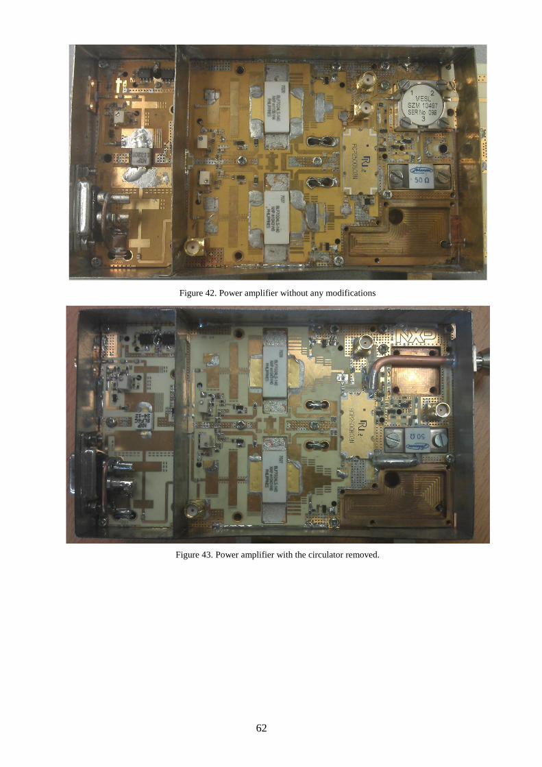
62
Figure 42. Power amplifier without any modifications
Figure 43. Power amplifier with the circulator removed.

63
4.3 PA Module Description
Figure 44 shows the block diagram of the PA module. In this PA there are two hybrids used as
power splitter (which splits a single signal and provides as two outputs) and the combiner
(which combines two inputs and provides as a single output signal) according to the need and the
orientation of the connections.
There are four ports in a hybrid. If the hybrid is to be used as a combiner then its two ports will
connected to the input of the transistors, one of which is with 90 degree phase shift. The third
port will be connected to the output and the forth port to the dummy load. In case of the splitter
hybrid two of its ports will be connected to the input ports with a 90 degree phase shift. The third
and fourth ports will be connected to the input and dummy load respectively. In the hybrid if
one port is determined then the other three ports are defined automatically. In the case of the PA
the first splitter hybrid is of small size and low cost as it handles less power while the other
combiner hybrid is big and costly as it handles higher power levels. Please refer [26] [27] for
data sheet of the hybrids.
The first hybrid has the input from the driver amplifier. The driver amplifier is the first stage of
the power amplifier block which performs the amplification of signal from the RF generation
board. This first hybrid performs the work of the splitter and provides the signal output at 2
branches. The split output from the hybrid is given to the gate of the RF transistors. One of
output from the hybrid is 90 degree phase shifted. The RF transistors amplify the given input
signal. The maximum output signal from each of the transistors is 140 watts.
The output signal from both the transistors is combined in the second hybrid. This hybrid has to
handle huge amount of input power, hence the size and the cost of this combiner is high. The
combiner used in the experiment can handle 300 watts at the system frequency.
The studied application requires a maximum of 250 watts signal power generated from each
power amplifier block. But with the design amplifier some more power can be generated in order
to compensate for various losses. These various losses can be due to hybrids or other
components. The third pin of the combiner is connected to the output. The fourth output of the
combiner is connected to the dummy 50 ohm load. This dummy load is used to terminate the
reflected power coming back into the hybrid.
The entire PCB of the PA along with the components is placed on copper plate and sealed. This
was done in order to dissipate the heat generated by the power amplifier module efficiently. The
total PA chain amplifies low power RF signal (about 1 Watts) generated by a RF generation
board to 250 Watts output by two step amplification.
Figure 44. Block diagram of the PA module.
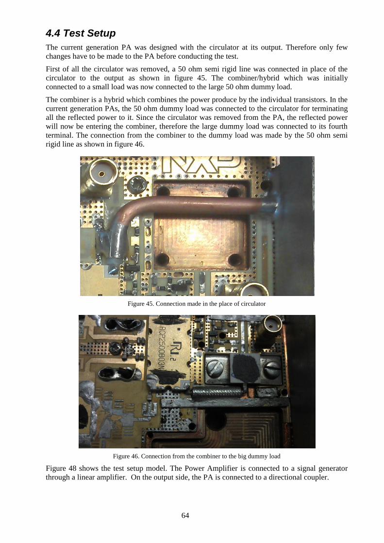
64
4.4 Test Setup
The current generation PA was designed with the circulator at its output. Therefore only few
changes have to be made to the PA before conducting the test.
First of all the circulator was removed, a 50 ohm semi rigid line was connected in place of the
circulator to the output as shown in figure 45. The combiner/hybrid which was initially
connected to a small load was now connected to the large 50 ohm dummy load.
The combiner is a hybrid which combines the power produce by the individual transistors. In the
current generation PAs, the 50 ohm dummy load was connected to the circulator for terminating
all the reflected power to it. Since the circulator was removed from the PA, the reflected power
will now be entering the combiner, therefore the large dummy load was connected to its fourth
terminal. The connection from the combiner to the dummy load was made by the 50 ohm semi
rigid line as shown in figure 46.
Figure 45. Connection made in the place of circulator
Figure 46. Connection from the combiner to the big dummy load
Figure 48 shows the test setup model. The Power Amplifier is connected to a signal generator
through a linear amplifier. On the output side, the PA is connected to a directional coupler.
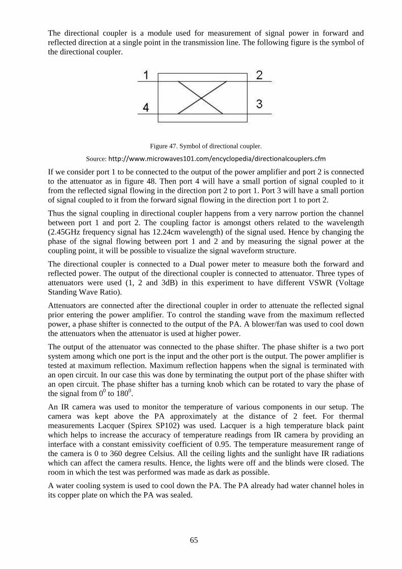
65
The directional coupler is a module used for measurement of signal power in forward and
reflected direction at a single point in the transmission line. The following figure is the symbol of
the directional coupler.
Figure 47. Symbol of directional coupler.
Source: http://www.microwaves101.com/encyclopedia/directionalcouplers.cfm
If we consider port 1 to be connected to the output of the power amplifier and port 2 is connected
to the attenuator as in figure 48. Then port 4 will have a small portion of signal coupled to it
from the reflected signal flowing in the direction port 2 to port 1. Port 3 will have a small portion
of signal coupled to it from the forward signal flowing in the direction port 1 to port 2.
Thus the signal coupling in directional coupler happens from a very narrow portion the channel
between port 1 and port 2. The coupling factor is amongst others related to the wavelength
(2.45GHz frequency signal has 12.24cm wavelength) of the signal used. Hence by changing the
phase of the signal flowing between port 1 and 2 and by measuring the signal power at the
coupling point, it will be possible to visualize the signal waveform structure.
The directional coupler is connected to a Dual power meter to measure both the forward and
reflected power. The output of the directional coupler is connected to attenuator. Three types of
attenuators were used (1, 2 and 3dB) in this experiment to have different VSWR (Voltage
Standing Wave Ratio).
Attenuators are connected after the directional coupler in order to attenuate the reflected signal
prior entering the power amplifier. To control the standing wave from the maximum reflected
power, a phase shifter is connected to the output of the PA. A blower/fan was used to cool down
the attenuators when the attenuator is used at higher power.
The output of the attenuator was connected to the phase shifter. The phase shifter is a two port
system among which one port is the input and the other port is the output. The power amplifier is
tested at maximum reflection. Maximum reflection happens when the signal is terminated with
an open circuit. In our case this was done by terminating the output port of the phase shifter with
an open circuit. The phase shifter has a turning knob which can be rotated to vary the phase of
the signal from 00 to 180
0.
An IR camera was used to monitor the temperature of various components in our setup. The
camera was kept above the PA approximately at the distance of 2 feet. For thermal
measurements Lacquer (Spirex SP102) was used. Lacquer is a high temperature black paint
which helps to increase the accuracy of temperature readings from IR camera by providing an
interface with a constant emissivity coefficient of 0.95. The temperature measurement range of
the camera is 0 to 360 degree Celsius. All the ceiling lights and the sunlight have IR radiations
which can affect the camera results. Hence, the lights were off and the blinds were closed. The
room in which the test was performed was made as dark as possible.
A water cooling system is used to cool down the PA. The PA already had water channel holes in
its copper plate on which the PA was sealed.
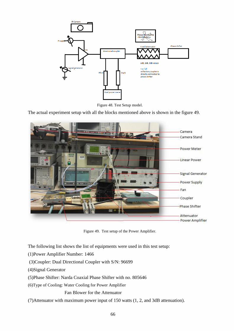
66
Figure 48. Test Setup model.
The actual experiment setup with all the blocks mentioned above is shown in the figure 49.
Figure 49. Test setup of the Power Amplifier.
The following list shows the list of equipments were used in this test setup:
(1)Power Amplifier Number: 1466
(3)Coupler: Dual Directional Coupler with S/N: 96699
(4)Signal Generator
(5)Phase Shifter: Narda Coaxial Phase Shifter with no. 805646
(6)Type of Cooling: Water Cooling for Power Amplifier
Fan Blower for the Attenuator
(7)Attenuator with maximum power input of 150 watts (1, 2, and 3dB attenuation).
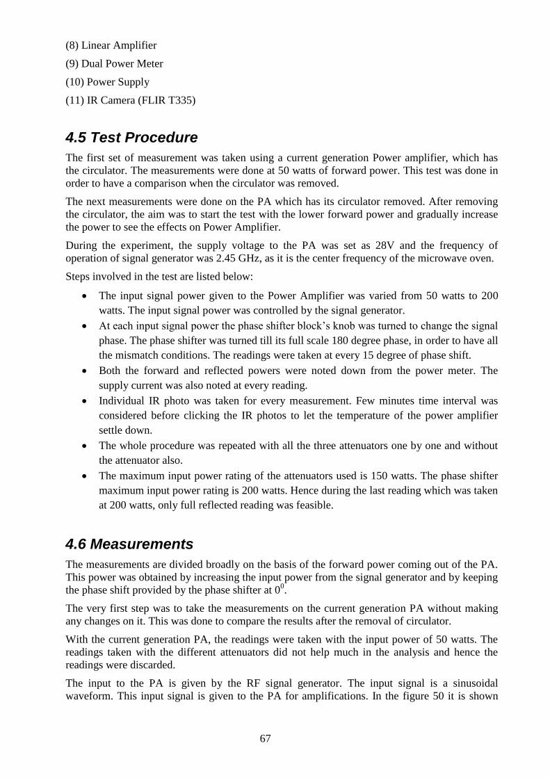
67
(8) Linear Amplifier
(9) Dual Power Meter
(10) Power Supply
(11) IR Camera (FLIR T335)
4.5 Test Procedure
The first set of measurement was taken using a current generation Power amplifier, which has
the circulator. The measurements were done at 50 watts of forward power. This test was done in
order to have a comparison when the circulator was removed.
The next measurements were done on the PA which has its circulator removed. After removing
the circulator, the aim was to start the test with the lower forward power and gradually increase
the power to see the effects on Power Amplifier.
During the experiment, the supply voltage to the PA was set as 28V and the frequency of
operation of signal generator was 2.45 GHz, as it is the center frequency of the microwave oven.
Steps involved in the test are listed below:
The input signal power given to the Power Amplifier was varied from 50 watts to 200
watts. The input signal power was controlled by the signal generator.
At each input signal power the phase shifter block‟s knob was turned to change the signal
phase. The phase shifter was turned till its full scale 180 degree phase, in order to have all
the mismatch conditions. The readings were taken at every 15 degree of phase shift.
Both the forward and reflected powers were noted down from the power meter. The
supply current was also noted at every reading.
Individual IR photo was taken for every measurement. Few minutes time interval was
considered before clicking the IR photos to let the temperature of the power amplifier
settle down.
The whole procedure was repeated with all the three attenuators one by one and without
the attenuator also.
The maximum input power rating of the attenuators used is 150 watts. The phase shifter
maximum input power rating is 200 watts. Hence during the last reading which was taken
at 200 watts, only full reflected reading was feasible.
4.6 Measurements
The measurements are divided broadly on the basis of the forward power coming out of the PA.
This power was obtained by increasing the input power from the signal generator and by keeping
the phase shift provided by the phase shifter at 00.
The very first step was to take the measurements on the current generation PA without making
any changes on it. This was done to compare the results after the removal of circulator.
With the current generation PA, the readings were taken with the input power of 50 watts. The
readings taken with the different attenuators did not help much in the analysis and hence the
readings were discarded.
The input to the PA is given by the RF signal generator. The input signal is a sinusoidal
waveform. This input signal is given to the PA for amplifications. In the figure 50 it is shown
68
that how the output signals from the PA should amplify the given input signal. For the proper
amplification it is very important that the transistors of the PA should be in saturation region. If
the transistors are in the triode/linear region then there will be no linear amplification and the
output signal will be non linear in magnitude compared to the input signal. During the operation
of the PA, if there is a change in the transistor operation from the saturation region to the linear
region due to improper biasing voltages, then it will generate random reduced magnitude output
signal. The following figure 50 shows the diagrammatic representation between an amplified
signal and the input signal.
Figure 50. Ideal waveform from the output of PA.
4.6.1 PA with Circulator Readings
In this experiment step where the PA with circulator was tested as shown in the figure 42, the
readings were taken only at full reflection condition. Full reflection condition was preferred in
this test because the PA has the circulator placed in it to protect the transistors from the reflected
signal power. The term full reflection means that the attenuators were not connected before the
phase shifter.
The black paint “Lacquer” was not applied on the PA when this test was conducted. In this case
without Lacquer, an error 50
Celsius in thermal readings is possible.
The readings were noted only after every 300 phase step. This relaxation in terms of larger phase
step and non usage of Lacquer were due to the reason that this test was just needed for
comparison.
The following table 11 shows the readings taken with this experiment setup.
69
Table 11. Measurements of PA with circulator
phase current (A)
Power (forward)
dBm
Power (Reflected)
dBm
Temperature1 Celsius upper
transistor
Temp2 Celsius
circulator
Temp3 Celsius lower
transistor
Temp4 Celsius
impedance
0 11.4 47.07 46.35 31.1 27.7 40.7 47.7
30 11.4 47.88 46.64 31 27.6 39.9 47.7
60 11.4 48.93 47.32 31.2 27.8 39.4 45.1
90 11.5 48.83 47.46 31.4 28.2 38.7 45.3
120 11.5 47.9 47.11 31.5 28.6 38.5 46.4
150 11.4 47.13 46.7 31.4 28.6 39.5 48
180 11.4 47.02 46.48 31.2 28.1 39.7 48.3
The following figure 51 shows one of the IR images taken during this experiment.
Figure51. Picture Taken by IR Camera on no input power.
This figure 51 describes the components as seen through the IR camera. Since the picture was
taken when there was no power supply given to the PA, all the components are at room
temperature. The PA has lot of components but in this test the main concern was on the
transistors, combiner and the load.
It was observed during the experiment, that the forward power varied from 48.93dBm to
47.02dBm while introducing a phase shift from 0 to180 degrees through the phase shifter.
It was also observed during the experiment that the reflected power followed the forward power
closely. The temperatures of the two transistors were same irrespective of the introduced phase
shift. This issue was analyzed and discussed later.

70
The following figure 52 shows the graph obtained from the measurements in table 11.
Figure 52. Graph between power and phase, at full reflection
The following figure 53 shows the transistor temperature variation with different phase shifts
from the measurements in table.
Figure 53. Graph between temperature of the transistors and the phase shift
It can be seen from the above figure 53 that the temperature of upper transistor is changing and
showing a sinusoidal variation. The lower transistor does not show this sinusoidal temperature
variation. The reason for the different temperature behavior of the two transistors is explained in
the section 4.7.
45
45.5
46
46.5
47
47.5
48
48.5
49
49.5
0 30 60 90 120 150 180
Po
we
r(d
Bm
)
Phase(degree)
Forward and reflected power
Power(forward) dBm
Power(Reflected) dBm
25
27
29
31
33
35
37
39
41
43
0 30 60 90 120 150 180
Tem
p(C
)
phase(degree)
transistors temperature
temperature1 Celsiusupper transistor
temp3 Celsius lowertransistor
71
4.6.2 Test without circulator
4.6.2.1 50 Watts forward power
After performing the test on the PA with circulator, the circulator was removed and changes
were made to the PA as mentioned in the section 4.4. This test was done various times to find all
the faults in the power Amplifier and make it perfect for the further test.
The following figure 54 shows the view of PA, showing the transistors, semi rigid line
connection in the place of circulator and the 50 ohm large dummy load. Notice here that the
below figure 54 shows the combined view of figure 45 and figure 46.
Figure 54. Power Amplifier with black test paint applied.
After the modifications were made on the Power Amplifier, the results showed very high
temperature on the load and on one of the transistors. The temperature on the load and the lower
transistor reached 50 degree Celsius with full reflection. Hence the black paint “Lacquer” which
is already mentioned in the previous section was applied on the Power Amplifier to make the
temperature readings more accurate. There was an increase in the overall temperature by
approximately 50 Celsius at various components after the Lacquer was applied.
The graph drawn from the temperature measurements of the upper and lower transistors is shown
below in figure 55. The figure55 shows the variation of transistor temperature with phase shift.
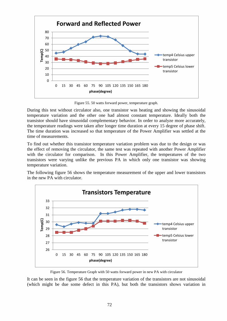
72
Figure 55. 50 watts forward power, temperature graph.
During this test without circulator also, one transistor was heating and showing the sinusoidal
temperature variation and the other one had almost constant temperature. Ideally both the
transistor should have sinusoidal complementary behavior. In order to analyze more accurately,
the temperature readings were taken after longer time duration at every 15 degree of phase shift.
The time duration was increased so that temperature of the Power Amplifier was settled at the
time of measurements.
To find out whether this transistor temperature variation problem was due to the design or was
the effect of removing the circulator, the same test was repeated with another Power Amplifier
with the circulator for comparison. In this Power Amplifier, the temperatures of the two
transistors were varying unlike the previous PA in which only one transistor was showing
temperature variation.
The following figure 56 shows the temperature measurement of the upper and lower transistors
in the new PA with circulator.
Figure 56. Temperature Graph with 50 watts forward power in new PA with circulator
It can be seen in the figure 56 that the temperature variation of the transistors are not sinusoidal
(which might be due some defect in this PA), but both the transistors shows variation in
0
10
20
30
40
50
60
70
80
0 15 30 45 60 75 90 105 120 135 150 165 180
Tem
p(C
)
phase(degree)
Forward and Reflected Power
temp4 Celsius uppertransistor
temp5 Celsius lowertransistor
26
27
28
29
30
31
32
33
0 15 30 45 60 75 90 105 120 135 150 165 180
Tem
p(C
)
phase(degree)
Transistors Temperature
temp4 Celsius uppertransistor
temp5 Celsius lowertransistor

73
correlation with each other. Note here that this figure 56 shows the temperature response of a PA
with circulator.
Comparing the figure 56 with the figure 53 shows the temperature behavior of the first PA
before removing the circulator, and it was concluded that the abnormal temperature behavior is
not due to the removal of circulator. Thus it can be clearly understood that the less temperature
variation in one of the transistor is due to improper design of the PA.
The analysis of the result of both the Power Amplifiers was performed and it was concluded that
the lower transistor was not soldered properly to the heat sink, due to which the heat transfer
from the transistor to the cooling system was not proper. This resulted in the constant
temperature of the transistor. The lower transistor was connected properly to the input and output
ports, hence it was handling only less power and the remaining output power was produced by
the upper transistor. This resulted in very high temperature variation in upper transistor and less
temperature variation in lower transistor.
To solve this problem in the PA being used, the lower transistor was re-soldered and small errors
due to soldering procedure like short circuit in the wires and burnout of capacitors was fixed. It
was noted in the PA that the dummy load was getting heated up very fast. The rise in the dummy
load temperature was solved by adding a thermal paste and screwing it again. The thermal paste
is the highly toxic paste which has better dielectric constant than that of air. This will help in fast
cooling of the dummy load by helping it to efficiently dissipate the heat to the heat sink.
After the above mentioned corrections were performed in the PA, the experiment was continued
and the measurements were taken.
The following figure 57 shows the IR image of the PA taken when the PA had 50 Watts forward
power.
Figure 57. Thermal picture of the Power Amplifier at 50 watts of Input.
At each phase shift the thermal pictures have been taken during the experiment.
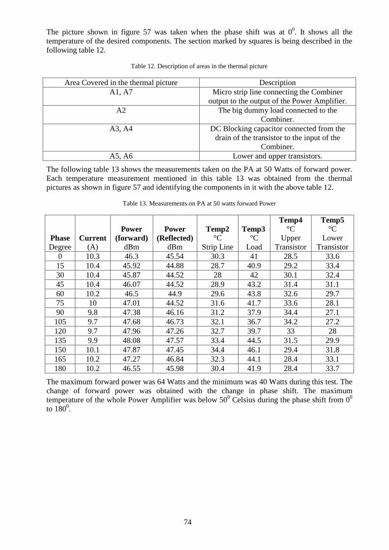
74
The picture shown in figure 57 was taken when the phase shift was at 00. It shows all the
temperature of the desired components. The section marked by squares is being described in the
following table 12.
Table 12. Description of areas in the thermal picture
Area Covered in the thermal picture Description
A1, A7 Micro strip line connecting the Combiner
output to the output of the Power Amplifier.
A2 The big dummy load connected to the
Combiner.
A3, A4 DC Blocking capacitor connected from the
drain of the transistor to the input of the
Combiner.
A5, A6 Lower and upper transistors.
The following table 13 shows the measurements taken on the PA at 50 Watts of forward power.
Each temperature measurement mentioned in this table 13 was obtained from the thermal
pictures as shown in figure 57 and identifying the components in it with the above table 12.
Table 13. Measurements on PA at 50 watts forward Power
Phase
Degree
Current
(A)
Power
(forward)
dBm
Power
(Reflected)
dBm
Temp2
°C
Strip Line
Temp3
°C
Load
Temp4
°C
Upper
Transistor
Temp5
°C
Lower
Transistor
0 10.3 46.3 45.54 30.3 41 28.5 33.6
15 10.4 45.92 44.88 28.7 40.9 29.2 33.4
30 10.4 45.87 44.52 28 42 30.1 32.4
45 10.4 46.07 44.52 28.9 43.2 31.4 31.1
60 10.2 46.5 44.9 29.6 43.8 32.6 29.7
75 10 47.01 44.52 31.6 41.7 33.6 28.1
90 9.8 47.38 46.16 31.2 37.9 34.4 27.1
105 9.7 47.68 46.73 32.1 36.7 34.2 27.2
120 9.7 47.96 47.26 32.7 39.7 33 28
135 9.9 48.08 47.57 33.4 44.5 31.5 29.9
150 10.1 47.87 47.45 34.4 46.1 29.4 31.8
165 10.2 47.27 46.84 32.3 44.1 28.4 33.1
180 10.2 46.55 45.98 30.4 41.9 28.4 33.7
The maximum forward power was 64 Watts and the minimum was 40 Watts during this test. The
change of forward power was obtained with the change in phase shift. The maximum
temperature of the whole Power Amplifier was below 500 Celsius during the phase shift from 0
0
to 1800.

75
The following figure 58 shows the variation of forward and reflected power with phase shift.
Figure 58.Graph showing the forward and reflected power variation with phase shift
In the graph shown in figure 58, the reflected power curves followed the forward power curves
closely, as expected. Here one can observed that approximately 95% of the power is reflected
back to the circuit, which is very good for observing the worst case scenario for the practical
approach. This reflection is obtained due to the open circuit impedance provided by the output
port of the phase shifter. Further no attenuator was used during this measurement, thus it
portraits the worst case scenario. These readings are obtained without the load, hence the loss in
the micro strip line contribute to the reduced value of the reflected power.
The following figure 59 shows the variation of temperature in the two transistors with phase
shift.
Figure 59. Graph showing the variation of temperature in transistors with phase shift
The figure 59 shows the temperature of the transistors varying from 350 to 28
0 Celsius. They
were varying properly with the phases as one transistors temperature goes up, the other
transistors goes down and vice versa. This can be interpreted as one of the transistors has more
load than the other with the phase change. This is the ideal behavior which was expected from
this test.
42
43
44
45
46
47
48
49
0 15 30 45 60 75 90 105 120 135 150 165 180
Po
we
r(d
Bm
)
Phase(degree)
50 Watts Forward and Reflected Power
Power(forward) dBm
Power(Reflected) dBm
20
22
24
26
28
30
32
34
36
0 15 30 45 60 75 90 105 120 135 150 165 180
Tem
p(C
)
phase(degree)
50 Watts, Transistor Temperature
temp4 Celsius uppertransistor
temp5 Celsius lowertransistor

76
The following figure 60 shows the variation of current consumed by the PA with different phase
shifts.
Figure 60. Graph showing the variation in the current consumption of the PA with phase shift
The current consumption was noted from the power supply block. The figure 60 shows the
current consumption varies from 9.7 Ampere to 10.4 Ampere during the phase shift from 00 to
1800. The current also shows the sinusoidal pattern during the phase shift. From the test
measurement in this step, we may conclude that the Power Amplifier can be used without the
circulator at this particular forward power, since the behavior of the forward and reflected power,
the current consumption and the temperature of transistors were all sinusoidal. The reason for the
sinusoidal behavior is explained in the later section 4.7.
9.2
9.4
9.6
9.8
10
10.2
10.4
10.6
0 15 30 45 60 75 90 105 120 135 150 165 180
Cu
rre
nt(
A)
phase(degree)
50 Watts,Current (A)
current (A)
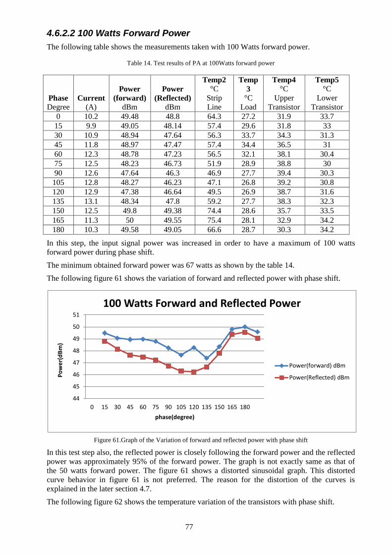
77
4.6.2.2 100 Watts Forward Power
The following table shows the measurements taken with 100 Watts forward power.
Table 14. Test results of PA at 100Watts forward power
Phase
Degree
Current
(A)
Power
(forward)
dBm
Power
(Reflected)
dBm
Temp2
°C
Strip
Line
Temp
3
°C
Load
Temp4
°C
Upper
Transistor
Temp5
°C
Lower
Transistor
0 10.2 49.48 48.8 64.3 27.2 31.9 33.7
15 9.9 49.05 48.14 57.4 29.6 31.8 33
30 10.9 48.94 47.64 56.3 33.7 34.3 31.3
45 11.8 48.97 47.47 57.4 34.4 36.5 31
60 12.3 48.78 47.23 56.5 32.1 38.1 30.4
75 12.5 48.23 46.73 51.9 28.9 38.8 30
90 12.6 47.64 46.3 46.9 27.7 39.4 30.3
105 12.8 48.27 46.23 47.1 26.8 39.2 30.8
120 12.9 47.38 46.64 49.5 26.9 38.7 31.6
135 13.1 48.34 47.8 59.2 27.7 38.3 32.3
150 12.5 49.8 49.38 74.4 28.6 35.7 33.5
165 11.3 50 49.55 75.4 28.1 32.9 34.2
180 10.3 49.58 49.05 66.6 28.7 30.3 34.2
In this step, the input signal power was increased in order to have a maximum of 100 watts
forward power during phase shift.
The minimum obtained forward power was 67 watts as shown by the table 14.
The following figure 61 shows the variation of forward and reflected power with phase shift.
Figure 61.Graph of the Variation of forward and reflected power with phase shift
In this test step also, the reflected power is closely following the forward power and the reflected
power was approximately 95% of the forward power. The graph is not exactly same as that of
the 50 watts forward power. The figure 61 shows a distorted sinusoidal graph. This distorted
curve behavior in figure 61 is not preferred. The reason for the distortion of the curves is
explained in the later section 4.7.
The following figure 62 shows the temperature variation of the transistors with phase shift.
44
45
46
47
48
49
50
51
0 15 30 45 60 75 90 105 120 135 150 165 180
Po
we
r(d
Bm
)
phase(degree)
100 Watts Forward and Reflected Power
Power(forward) dBm
Power(Reflected) dBm
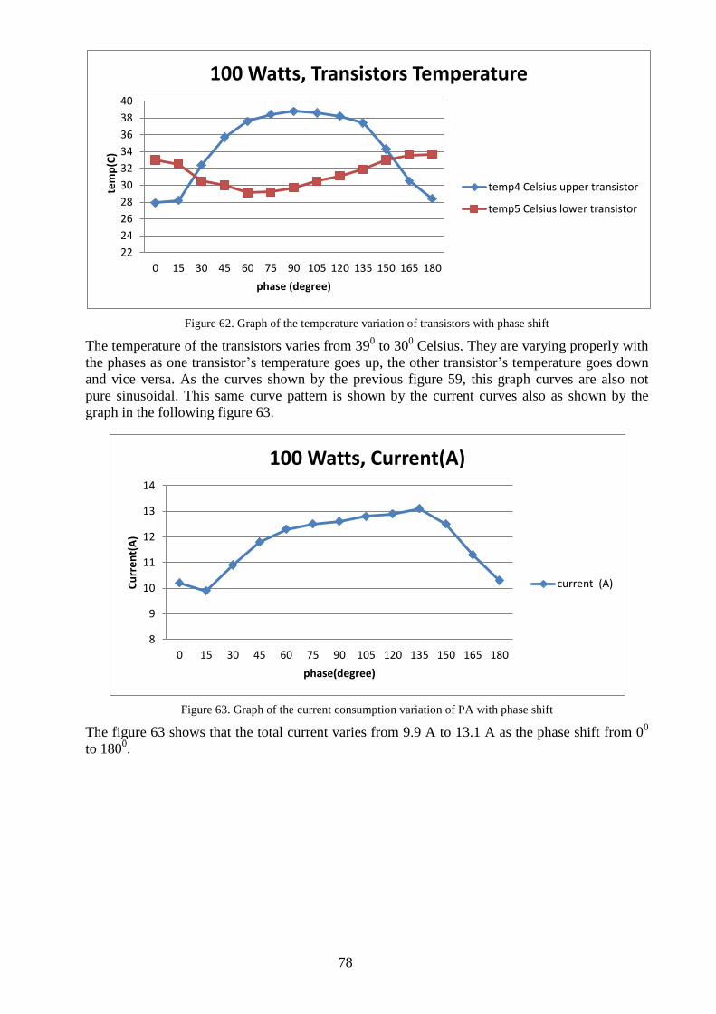
78
Figure 62. Graph of the temperature variation of transistors with phase shift
The temperature of the transistors varies from 390 to 30
0 Celsius. They are varying properly with
the phases as one transistor‟s temperature goes up, the other transistor‟s temperature goes down
and vice versa. As the curves shown by the previous figure 59, this graph curves are also not
pure sinusoidal. This same curve pattern is shown by the current curves also as shown by the
graph in the following figure 63.
Figure 63. Graph of the current consumption variation of PA with phase shift
The figure 63 shows that the total current varies from 9.9 A to 13.1 A as the phase shift from 00
to 1800.
22
24
26
28
30
32
34
36
38
40
0 15 30 45 60 75 90 105 120 135 150 165 180
tem
p(C
)
phase (degree)
100 Watts, Transistors Temperature
temp4 Celsius upper transistor
temp5 Celsius lower transistor
8
9
10
11
12
13
14
0 15 30 45 60 75 90 105 120 135 150 165 180
Cu
rre
nt(
A)
phase(degree)
100 Watts, Current(A)
current (A)
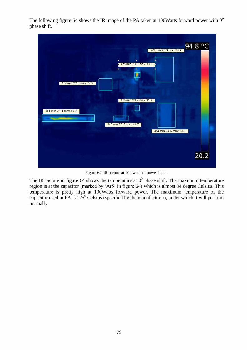
79
The following figure 64 shows the IR image of the PA taken at 100Watts forward power with 00
phase shift.
Figure 64. IR picture at 100 watts of power input.
The IR picture in figure 64 shows the temperature at 00 phase shift. The maximum temperature
region is at the capacitor (marked by „Ar5‟ in figure 64) which is almost 94 degree Celsius. This
temperature is pretty high at 100Watts forward power. The maximum temperature of the
capacitor used in PA is 1250 Celsius (specified by the manufacturer), under which it will perform
normally.
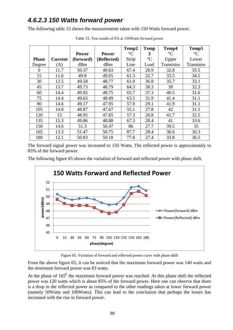
80
4.6.2.3 150 Watts forward power
The following table 15 shows the measurements taken with 150 Watts forward power.
Table 15. Test results of PA at 150Watts forward power
Phase
Degree
Current
(A)
Power
(forward)
dBm
Power
(Reflected)
dBm
Temp2
°C
Strip
Line
Temp
3
°C
Load
Temp4
°C
Upper
Transistor
Temp5
°C
Lower
Transistor
0 11.7 50.37 49.63 67.4 28.9 32.8 35.5
15 11.6 49.8 49.05 61.3 32.7 33.5 34.5
30 12.5 49.58 48.77 61.9 36.8 35.7 33.1
45 13.7 49.73 48.79 64.3 38.3 38 32.3
60 14.4 49.82 48.75 65.7 37.3 40.5 31.6
75 14.4 49.63 48.49 63.5 31.9 41.4 31.1
90 14.6 49.17 47.95 57.9 29.1 41.9 31.1
105 14.8 48.87 47.67 55.1 27.8 42 31.5
120 15 48.95 47.85 57.3 26.8 41.7 32.5
135 15.3 49.86 48.88 67.3 28.4 41 33.6
150 14.6 51.3 50.47 86 27.7 39.5 35
165 13.3 51.47 50.75 87.7 28.4 36.6 36.3
180 12.1 50.83 50.18 77.8 27.4 33.8 36.5
The forward signal power was increased to 150 Watts. The reflected power is approximately to
85% of the forward power.
The following figure 65 shows the variation of forward and reflected power with phase shift.
Figure 65. Variation of forward and reflected power curve with phase shift
From the above figure 65, it can be noticed that the maximum forward power was 140 watts and
the minimum forward power was 83 watts.
At the phase of 1650 the maximum forward power was reached. At this phase shift the reflected
power was 120 watts which is about 85% of the forward power. Here one can observe that there
is a drop in the reflected power as compared to the other readings taken at lower forward power
(namely 50Watts and 100Watts). This can lead to the conclusion that perhaps the losses has
increased with the rise in forward power.
45
46
47
48
49
50
51
52
0 15 30 45 60 75 90 105 120 135 150 165 180
po
we
r(d
Bm
)
phase(degree)
150 Watts Forward and Reflected Power
Power(forward) dBm
Power(Reflected) dBm
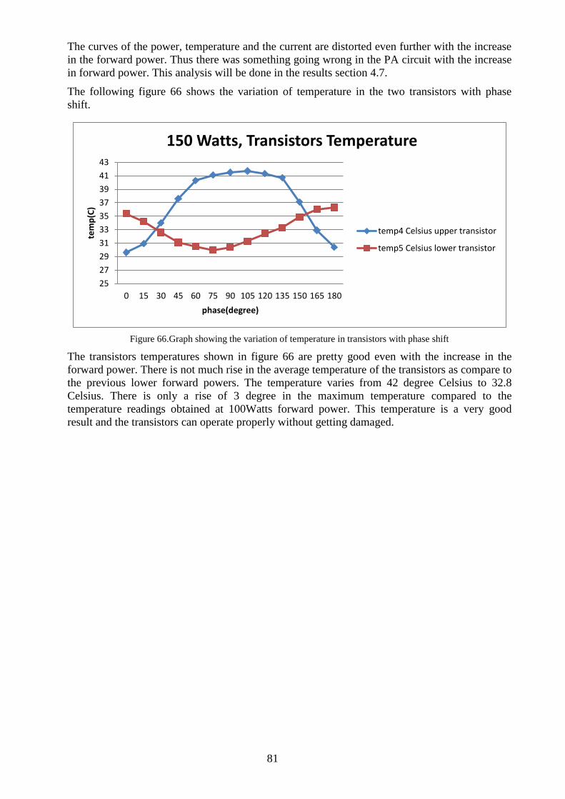
81
The curves of the power, temperature and the current are distorted even further with the increase
in the forward power. Thus there was something going wrong in the PA circuit with the increase
in forward power. This analysis will be done in the results section 4.7.
The following figure 66 shows the variation of temperature in the two transistors with phase
shift.
Figure 66.Graph showing the variation of temperature in transistors with phase shift
The transistors temperatures shown in figure 66 are pretty good even with the increase in the
forward power. There is not much rise in the average temperature of the transistors as compare to
the previous lower forward powers. The temperature varies from 42 degree Celsius to 32.8
Celsius. There is only a rise of 3 degree in the maximum temperature compared to the
temperature readings obtained at 100Watts forward power. This temperature is a very good
result and the transistors can operate properly without getting damaged.
25
27
29
31
33
35
37
39
41
43
0 15 30 45 60 75 90 105 120 135 150 165 180
tem
p(C
)
phase(degree)
150 Watts, Transistors Temperature
temp4 Celsius upper transistor
temp5 Celsius lower transistor
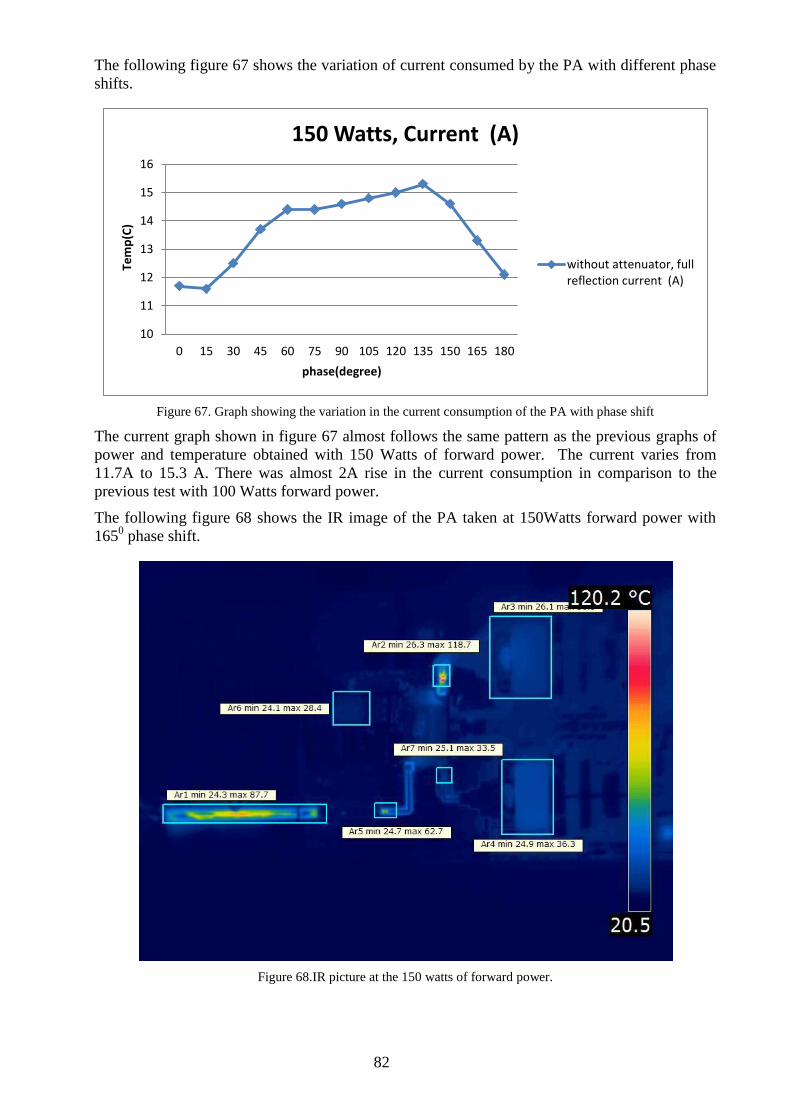
82
The following figure 67 shows the variation of current consumed by the PA with different phase
shifts.
Figure 67. Graph showing the variation in the current consumption of the PA with phase shift
The current graph shown in figure 67 almost follows the same pattern as the previous graphs of
power and temperature obtained with 150 Watts of forward power. The current varies from
11.7A to 15.3 A. There was almost 2A rise in the current consumption in comparison to the
previous test with 100 Watts forward power.
The following figure 68 shows the IR image of the PA taken at 150Watts forward power with
1650 phase shift.
Figure 68.IR picture at the 150 watts of forward power.
10
11
12
13
14
15
16
0 15 30 45 60 75 90 105 120 135 150 165 180
Tem
p(C
)
phase(degree)
150 Watts, Current (A)
without attenuator, fullreflection current (A)
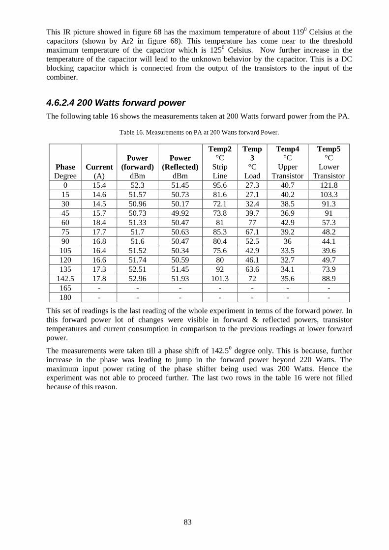
83
This IR picture showed in figure 68 has the maximum temperature of about 1190 Celsius at the
capacitors (shown by Ar2 in figure 68). This temperature has come near to the threshold
maximum temperature of the capacitor which is 1250 Celsius. Now further increase in the
temperature of the capacitor will lead to the unknown behavior by the capacitor. This is a DC
blocking capacitor which is connected from the output of the transistors to the input of the
combiner.
4.6.2.4 200 Watts forward power
The following table 16 shows the measurements taken at 200 Watts forward power from the PA.
Table 16. Measurements on PA at 200 Watts forward Power.
Phase
Degree
Current
(A)
Power
(forward)
dBm
Power
(Reflected)
dBm
Temp2
°C
Strip
Line
Temp
3
°C
Load
Temp4
°C
Upper
Transistor
Temp5
°C
Lower
Transistor
0 15.4 52.3 51.45 95.6 27.3 40.7 121.8
15 14.6 51.57 50.73 81.6 27.1 40.2 103.3
30 14.5 50.96 50.17 72.1 32.4 38.5 91.3
45 15.7 50.73 49.92 73.8 39.7 36.9 91
60 18.4 51.33 50.47 81 77 42.9 57.3
75 17.7 51.7 50.63 85.3 67.1 39.2 48.2
90 16.8 51.6 50.47 80.4 52.5 36 44.1
105 16.4 51.52 50.34 75.6 42.9 33.5 39.6
120 16.6 51.74 50.59 80 46.1 32.7 49.7
135 17.3 52.51 51.45 92 63.6 34.1 73.9
142.5 17.8 52.96 51.93 101.3 72 35.6 88.9
165 - - - - - - -
180 - - - - - - -
This set of readings is the last reading of the whole experiment in terms of the forward power. In
this forward power lot of changes were visible in forward & reflected powers, transistor
temperatures and current consumption in comparison to the previous readings at lower forward
power.
The measurements were taken till a phase shift of 142.50 degree only. This is because, further
increase in the phase was leading to jump in the forward power beyond 220 Watts. The
maximum input power rating of the phase shifter being used was 200 Watts. Hence the
experiment was not able to proceed further. The last two rows in the table 16 were not filled
because of this reason.
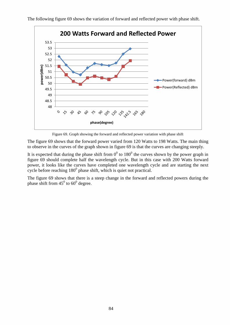
84
The following figure 69 shows the variation of forward and reflected power with phase shift.
Figure 69. Graph showing the forward and reflected power variation with phase shift
The figure 69 shows that the forward power varied from 120 Watts to 198 Watts. The main thing
to observe in the curves of the graph shown in figure 69 is that the curves are changing steeply.
It is expected that during the phase shift from 00 to 180
0 the curves shown by the power graph in
figure 69 should complete half the wavelength cycle. But in this case with 200 Watts forward
power, it looks like the curves have completed one wavelength cycle and are starting the next
cycle before reaching 1800 phase shift, which is quiet not practical.
The figure 69 shows that there is a steep change in the forward and reflected powers during the
phase shift from 450 to 60
0 degree.
48
48.5
49
49.5
50
50.5
51
51.5
52
52.5
53
53.5p
ow
er(
dB
m)
phase(degree)
200 Watts Forward and Reflected Power
Power(forward) dBm
Power(Reflected) dBm
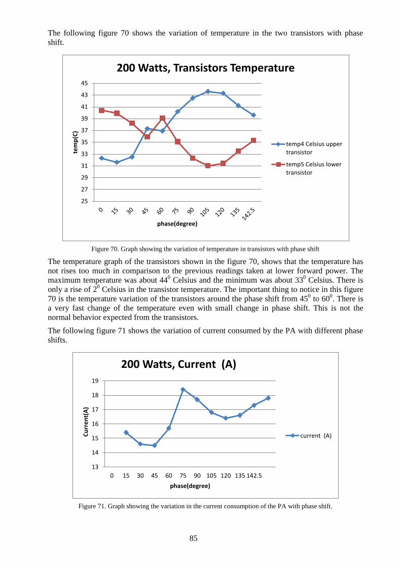
85
The following figure 70 shows the variation of temperature in the two transistors with phase
shift.
Figure 70. Graph showing the variation of temperature in transistors with phase shift
The temperature graph of the transistors shown in the figure 70, shows that the temperature has
not rises too much in comparison to the previous readings taken at lower forward power. The
maximum temperature was about 440 Celsius and the minimum was about 33
0 Celsius. There is
only a rise of 20 Celsius in the transistor temperature. The important thing to notice in this figure
70 is the temperature variation of the transistors around the phase shift from 450 to 60
0. There is
a very fast change of the temperature even with small change in phase shift. This is not the
normal behavior expected from the transistors.
The following figure 71 shows the variation of current consumed by the PA with different phase
shifts.
Figure 71. Graph showing the variation in the current consumption of the PA with phase shift.
25
27
29
31
33
35
37
39
41
43
45
tem
p(C
)
phase(degree)
200 Watts, Transistors Temperature
temp4 Celsius uppertransistor
temp5 Celsius lowertransistor
13
14
15
16
17
18
19
0 15 30 45 60 75 90 105 120 135 142.5
Cu
rre
nt(
A)
phase(degree)
200 Watts, Current (A)
current (A)
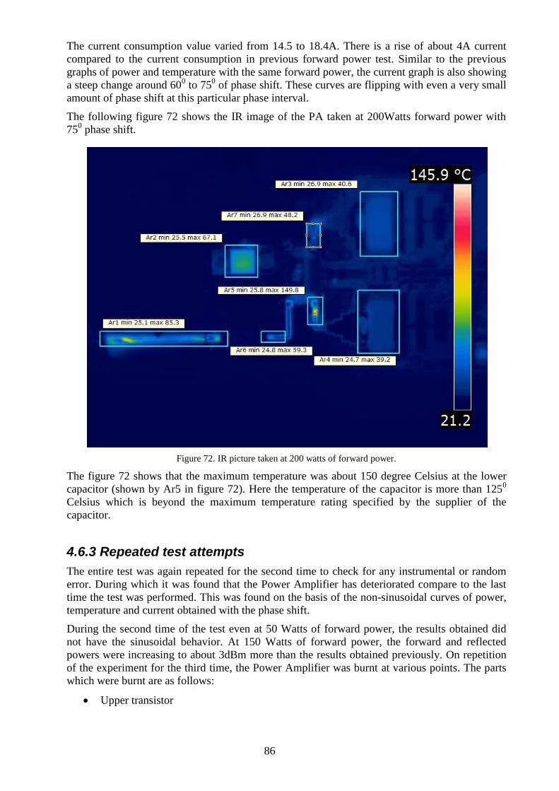
86
The current consumption value varied from 14.5 to 18.4A. There is a rise of about 4A current
compared to the current consumption in previous forward power test. Similar to the previous
graphs of power and temperature with the same forward power, the current graph is also showing
a steep change around 600 to 75
0 of phase shift. These curves are flipping with even a very small
amount of phase shift at this particular phase interval.
The following figure 72 shows the IR image of the PA taken at 200Watts forward power with
750 phase shift.
Figure 72. IR picture taken at 200 watts of forward power.
The figure 72 shows that the maximum temperature was about 150 degree Celsius at the lower
capacitor (shown by Ar5 in figure 72). Here the temperature of the capacitor is more than 1250
Celsius which is beyond the maximum temperature rating specified by the supplier of the
capacitor.
4.6.3 Repeated test attempts
The entire test was again repeated for the second time to check for any instrumental or random
error. During which it was found that the Power Amplifier has deteriorated compare to the last
time the test was performed. This was found on the basis of the non-sinusoidal curves of power,
temperature and current obtained with the phase shift.
During the second time of the test even at 50 Watts of forward power, the results obtained did
not have the sinusoidal behavior. At 150 Watts of forward power, the forward and reflected
powers were increasing to about 3dBm more than the results obtained previously. On repetition
of the experiment for the third time, the Power Amplifier was burnt at various points. The parts
which were burnt are as follows:
Upper transistor

87
Combiner
Input DC blocking Capacitor.
4.7 Analysis of results and future work
The sinusoidal behavior of each forward and reflected power with phase shift is due to the fact
that we are trying to reconstruct the standing wave present in transmission channel after the PA.
The standing wave voltage in the transmission channel is the resultant of forward and reflected
voltages. The forward and reflected power is measured at a small section of the transmission
channel in the directional coupler. This forward and reflected power is an estimate of the
sinusoidal standing wave and thus is an estimate of the VSWR at the output of PA.
This small section in the directional coupler where the forward and reflected power were being
measured corresponds to a fraction of the wavelength of the RF signal‟s wavelength. By
changing the phase of the reflected signal with the help of phase shifter, it is possible to sweep
the standing wave‟s position across the directional coupler‟s measurement section. The
interpolation of the forward and reflected power measurements for all the phase shifts would
result in visualizing the standing wave power structure. Thus a sinusoidal power graph is
expected while introducing a phase shift from 00 to 180
0.
The following figure 73 shows the standing wave in a transmission line under full reflection
condition and how it is related to the forward and reflected wave at a particular time instant.
Figure 73. Illustration of the standing waves.
Source: http://www.bessernet.com/Ereflecto/tutorialFrameset.htm
The above figure 73 shows the forward and reflected waves (in the upper plot) and the resultant
and standing waves (in the lower plot). The forward, reflected and resultant waves all travels at
the speed of light. Hence the standing wave will be the only waveform constructed with the
measurement values.
Thus the forward and reflected power measurements will trace the standing wave pattern in the
transmission line after the Power Amplifier.

88
The change of the graph from sinusoidal behavior to random is due to the mismatch in the
biasing of the transistors. The drain and gate voltage of the RF transistors has a fixed value,
which is done by “load pull method”. The load pull method is the company‟s internal method for
the proper biasing of the transistor.
When the circulator was removed from the output of the Power Amplifier, then huge amount of
the reflected power was going inside PA. The biasing of the transistor was not done for such a
huge amount of reflected power. „Biasing‟ of the transistor means the procedure, in which the
drain current of the RF transistor is set by adjusting the gate to source voltage with a constant
voltage bias source. The transistors in the PA has been biased at 10-30mA of drain current. In
this PA, a large potentiometer is used to set the bias current. But due to the reflected power, the
drain to source current is increased by few Amperes. This causes the strange behavior by the
PA.
The drain voltage gives a feedback to the gate bias voltage, especially if the impedance is high
on the input side. The input impedance is set to be high in tested PA as per the design. Thus the
PA which is used has a tendency to give a feedback voltage from drain to gate.
The increase in drain voltage causes the rise of gate voltage due to the feedback. The gate
voltage dependency to the drain voltage is caused by the rectifying effect of the ESD diode
inside the LDMOS transistor. This effect is most visible with a high drain voltage (large
mismatch) and high gate series resistor (around 10 ohms).
Hence the drain voltage increase due to the high reflected power was the main cause which
influences the mismatch levels and resulted in distorted curves in the graph.
The LDMOS transistors are biased in the Power Amplifier to operate in Class B mode. The two
transistors in the 2nd
stage of PA give half the output waveform (Class B operation) at 900 phase
difference. These two waves are combined by the hybrid to give out the full sinusoidal
waveform.
Due to the high reflected power resulting in high gate voltage, the mode of operation of the
transistors changes from Class B to Class A. In Class A operation, the transistors give out full
waveform as output. These two full wave forms when they are combined in a hybrid, then it
results in a reduced amplitude waveform output.
The following figure 74 shows the scenario in which due to high reflection, the output waveform
amplitude gets decreased.
Figure 74. Example of a resultant waveform when PA switching between classes.
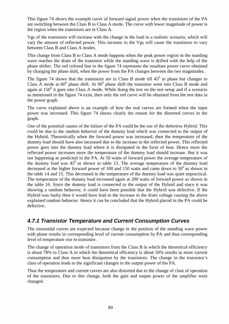
89
This figure 74 shows the example curve of forward signal power when the transistors of the PA
are switching between the Class B to Class A mode. The curve with lower magnitude of power is
the region when the transistors are in Class A.
Vgs of the transistors will increase with the change in the load in a realistic scenario, which will
vary the amount of reflected power. This increase in the Vgs will cause the transistors to vary
between Class B and Class A modes.
This change from Class B to Class A mode happens when the peak power region in the standing
wave reaches the drain of the transistor while the standing wave is drifted with the help of the
phase shifter. The red colored line in the figure 74 represents the resultant power curve obtained
by changing the phase shift, when the power from the PA changes between the two magnitudes.
The figure 74 shows that the transistors are in Class B mode till 450 in phase but changes to
Class A mode at 600 phase shift. At 90
0 phase shift the transistor went into Class B mode and
again at 1500 it goes into Class A mode. While doing the test on the test setup and if a scenario
as mentioned in the figure 74 exist, then only the red curve will be obtained from the test data in
the power graph.
The curve explained above is an example of how the real curves are formed when the input
power was increased. This figure 74 shows clearly the reason for the distorted curves in the
graph.
One of the potential causes of the failure of the PA could be the use of the defective Hybrid. This
could be due to the random behavior of the dummy load which was connected to the output of
the Hybrid. Theoretically when the forward power was increased, then the temperature of the
dummy load should have also increased due to the increase in the reflected power. This reflected
power goes into the dummy load where it is dissipated in the form of heat. Hence more the
reflected power increases more the temperature of the dummy load should increase. But it was
not happening as predicted in the PA. At 50 watts of forward power the average temperature of
the dummy load was 450
as shown in table 13. The average temperature of the dummy load
decreased at the higher forward power of 100 and 150 watts and came down to 300
as shown in
the table 14 and 15. This decreased in the temperature of the dummy load was quiet unpractical.
The temperature of the dummy load increased again at 200 watts of forward power as shown in
the table 16. Since the dummy load is connected to the output of the Hybrid and since it was
showing a random behavior, it could have been possible that the Hybrid was defective. If the
Hybrid was faulty then it would have lead to the increase in the drain voltage causing the above
explained random behavior. Hence it can be concluded that the Hybrid placed in the PA could be
defective.
4.7.1 Transistor Temperature and Current Consumption Curves
The sinusoidal curves are expected because change in the position of the standing wave power
with phase results in corresponding level of current consumption by PA and thus corresponding
level of temperature rise in transistor.
The change of operation mode of transistors from the Class B in which the theoretical efficiency
is about 78% to Class A in which the theoretical efficiency is about 50% results in more current
consumption and thus more heat dissipation by the transistors. The change in the transistor‟s
class of operation leads to the significant changes in the output power of the PA.
Thus the temperature and current curves are also distorted due to the change of class of operation
of the transistors. Due to this change, both the gain and output power of the amplifier were
changed.

90
A new PA has to be tested with a maximum forward power of 100 watts. The high series resistor
in PA will be replaced by a lower value resistor of about half the present value to see any
changes in the mismatch. This value of the resistor will be further reduced till any remarkable
difference appears in the measurements.
91
5 CONCLUSION AND FUTURE WORK
The work done in all the three sections namely on the transistor, pallet and the power amplifier
are all in the initial stage of experiment. These works need lot more time to decide that the
experiments will be successful or not. The time was the biggest constraint in all the works
mentioned in this thesis report. In all of them manufacturing was involved which is also a
constraint in getting a fast results. But all the given tasks were successfully completed.
The first section was about the packaging of transistor. There were changes made in the
packaging material of the transistor. PCB material „lead‟ for the gate and drain were used instead
of the conventional „lead frames‟. The change in the packaging material will lead to simplicity in
the manufacturing process. The DC test results of the transistor were close to the ideal values
except the thermal resistance value which were double the ideal values. This change in the
thermal resistance was due to the changed PCB material and height of the flanged used in the
new transistor. The future work for the transistor is to change the wire bonding and the mos
capacitance according to the changes made in the design. There is also a need of performing „RF
test‟ which can be only done after tuning the transistor properly.
The second section was about the microwave pallet which had a use of the transistor designed in
the first section of this report. This pallet was used for the frequency band of 2900MHz to
3300MHz.This pallet gave positive results for the future work. While testing the pallet, it was
concluded that the pallet had many areas to work upon. Firstly the correct transistor needs to be
manufactured again on the pallet. Then the external tuning and coupling of the pallet is required
to match the newly designed transistor with the already built in electrical network of the pallet.
This tuning will optimise the pallet to its best performance. If this generates favourable results,
then optimization of the design along with electrical matching network design has to be done.
Thus lot of work needs to be done in the pallet design, since it is at the initial stage of
development.
The third section was about the testing of the power amplifier without the circulator at the
output. The testing was done to reduce the size and the cost of the PA. The test results did not
show much favourable results at higher power. This was due to the change in the class of
operation of the PA from class B to class A. But it was too early to decide that whether the
experiment was a successful or not as the changes in the matching network is yet to be done.
These changes will prevent the unwanted switch in the class of operation in the PA and would
result in successful removal of the circulator from the PA design.
These are the few suggested future works which needs to be done on work discussed in various
sections of this report.

92
93
6 REFERENCES
[1] S. J.C.H. Theeuwen, and J.H. Qureshi, “LDMOS technology for RF power amplifiers”, IEEE
Transactions on Microwave Theory and Techniques (special issue on Power Amplifiers),
Volume 60, Issue 6, Part 2, pp. 1755-1763 (2012)
[2] NXP Semiconductor B.V Company internal and confidential data.
[3]Accuratus Cooperation, “Aluminum Oxide material characteristics”,
http://accuratus.com/alumox.html, accessed 2012-09-02.
[4] Plansee Group, “heat sinks”, http://www.plansee.com/en/Products-Heat-sinks-Heat-
spreaders-495.htm, accessed 2012-09-02.
[5] Jack Browne, “Ceramic for high power packages”,
electronicdesign.com/content/content/63382/108ED_FAQ.pdf, accessed 2012-09-04.
[6]Wikipedia, “Brazing”, http://en.wikipedia.org/wiki/Brazing, accessed 2012-09-04.
[7] Wolverine Joining Technologies, “Silver Alloy B72 information”,
http://www.silvaloy.com/brazing_detail.php?pid=41, accessed 2012-09-25.
[8] Kovar Technical Data,“ Kovar Alloy”,
http://www.hightempmetals.com/techdata/hitempKovardata.php, accesssed 2012-09-25.
[9] NXP Semiconductors, “LDMOS RF application”,
http://www.nxp.com/techzones/hprf-techzone/technologies/ldmos.html, accessed 2012-09-25.
[10] Schloemann, E., "Miniature circulators," Magnetics, IEEE Transactions on, vol.25, no.5,
pp.3236-3241, Sep 1989 DOI: 10.1109/20.42265.
URL: http://ieeexplore.ieee.org/stamp/stamp.jsp?tp=&arnumber=42265&isnumber=1621.
[11] Philips Semiconductors, “Circulators and Isolators unique passive devices”,
http://www.g1sle.com/files/downloads/circulator.pdf, accessed 2012-09-25.
[12] Ahmed Hemani, “Low power design 1”,
http://www.ict.kth.se/courses/IL2200/Lec/Low%20Power%20Intro.pdf, accessed 2012-09-25.
[13] Behzad Razavi, “Basic Concepts in RF Design”, RF microelectronics, 1998, pp 11-53.
[14] Kevti Foundation, “Kovar Properties”, http://kevtifoundation.org/pdfs/Kovar.pdf, accessed
2012-09-25.
[15] Materion, “Plated Flanges”,
http://materion.com/Products/ProductGroups/MicroelectronicsPackagingMaterials/CeramicPack
ages/PlatedFlanges.aspx, accessed 2012-09-25.
[16] NXP Semiconductors,“ Power LDMOS transistor BLF7G20L-200 ”
http://www.nxp.com/documents/data_sheet/BLF7G20L-200_7G20LS-200.pdf,
accessed 2012-09-27.
[17] Plansee Group, “Copper Molybdenum Heatsinks”, http://www.plansee-
tms.com/TI_CuMoCuCu_Laminates.pdf, accessed 2012-09-25.
[18] Rogers Corporation,“ Data sheet of RO3006”,
http://www.rogerscorp.com/documents/722/acm/RO3000-Laminate-Data-Sheet-RO3003-
RO3006-RO3010.aspx, accessed 2012-09-27.
94
[19] Rogers Corporation, “Datasheet of RO4350B”,
http://www.rogerscorp.com/documents/726/acm/RO4000-Laminates-data-sheet-and-fabrication-
guidelines-RO4003C-RO4350B.aspx, accessed 2012-09-27.
[20] Berkeley University,“Fundamentals wireless communication”,
http://www.eecs.berkeley.edu/~dtse/Chapters_PDF/Fundamentals_Wireless_Communication_ch
apter1.pdf, accessed 2012-09-25.
[21] Wikipedia,“Radio Frequency”, http://en.wikipedia.org/wiki/Radio_frequency, accessed
2012-09-25.
[22] CCRI,“Radio Frequency and Antenna Fundamentals”,http://faculty.ccri.edu/jbernardini/JB-
Website/ETEK1500/1500Notes/CWNA-ed4-Chapter-2.pdf, accessed 2012-09-25
[23] Mihai Albulet, “RF Power Amplifier”,
http://books.google.com/books?id=HrDXZctHzUQC&printsec=frontcover#v=onepage&q&f=fal
se, accessed 2012-09-25.
[24] NXP Semiconductors, “Datasheet of BLS6G2933P-200”,
http://www.nxp.com/documents/data_sheet/BLS6G2933P-200.pdf, accessed 2012-09-27.
[25] Microwaves10, “Introduction to S-parameters”,
http://www.microwaves101.com/encyclopedia/sparameters.cfm, accessed 2012-09-27.
[26] RN2 technologies, “ RCP2500B03N data sheet”,
http://www.google.com/url?sa=t&rct=j&q=&esrc=s&source=web&cd=1&cad=rja&ved=0CDw
QFjAA&url=http%3A%2F%2Fwww.epartshub.com%2Finclude%2Fcommon_fileAttach.jsp%3
Ffilename%3D00006134-
Specification%2520Sheet%2520RCP2500B03N%2520Rev1.pdf%26cmpyCd%3D00006134%2
6type%3Dpartsdoc&ei=rUFkUOb7AY7esgaR2IGYBw&usg=AFQjCNFOYIcSjRyQy2egcK6dq
dMMWYUdeg, accessed 2012-09-27.
[27] Anaren Microwave, “Hybrid Coupler 1P603S”,
http://www.anaren.com/sites/default/files/1P603%20Rev%20C%20Datasheet.pdf,
accessed 2012-09-27.
[28] Torreyhillstech, “Comparison of different flanges” http://www.torreyhillstech.com/qa.html,
accessed 2012-09-27.
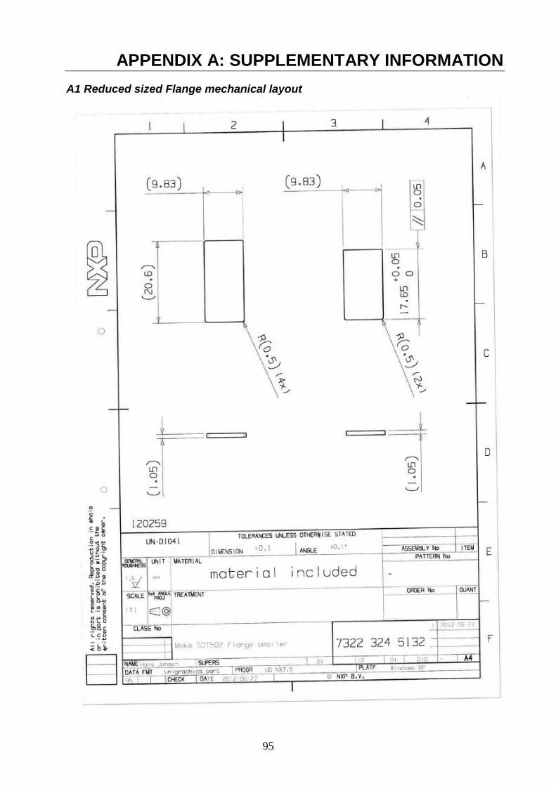
95
APPENDIX A: SUPPLEMENTARY INFORMATION
A1 Reduced sized Flange mechanical layout

96
A2 Slug tuner
“An impedance transformer comprising one or more longitudinally adjustable pieces of metal or
dielectric in a transmission line” http://www.encyclo.co.uk/define/slug%20tuner
Figure Slug tuner
In other words slug tuner changes the impedance manually. By changing the metal pieces one
can change the impedance point by point. This also helps in phase shifting as phase shift is
directly proportional to the wavelength. This helps in matching the network externally.


![RF Circuit Design - [Ch4-1] Microwave Transistor Amplifier](https://img.pdfslide.us/doc/110x75/55cc6094bb61eb9d338b474f/rf-circuit-design-ch4-1-microwave-transistor-amplifier.jpg)