Embed Size (px)
Citation preview
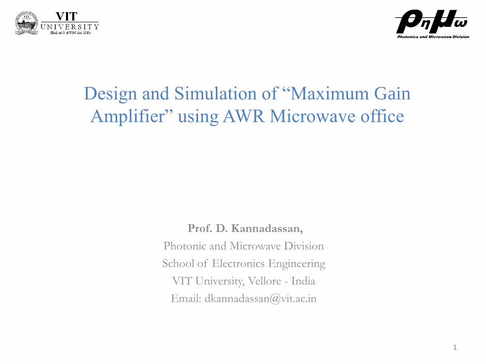
Design and Simulation of “Maximum Gain
Amplifier” using AWR Microwave office
Prof. D. Kannadassan,
Photonic and Microwave Division
School of Electronics Engineering
VIT University, Vellore - India
Email: [email protected]
1
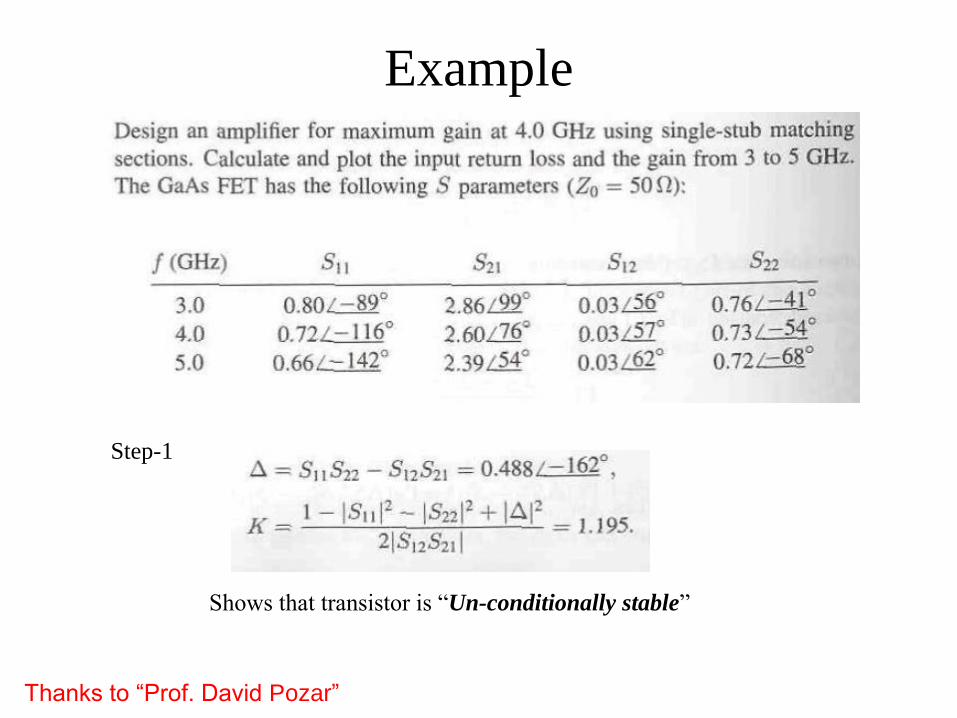
Example
Step-1
Shows that transistor is “Un-conditionally stable”
Thanks to “Prof. David Pozar”
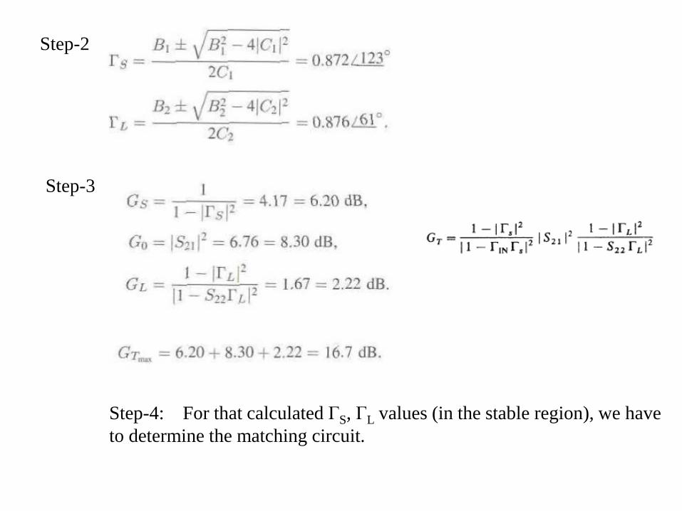
Step-2
Step-3
Step-4: For that calculated ΓS, ΓL values (in the stable region), we have
to determine the matching circuit.
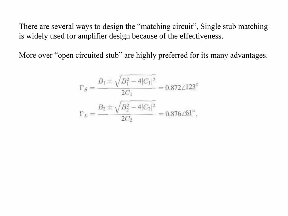
There are several ways to design the “matching circuit”, Single stub matching
is widely used for amplifier design because of the effectiveness.
More over “open circuited stub” are highly preferred for its many advantages.
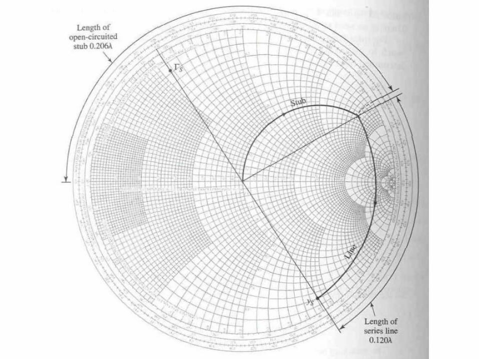
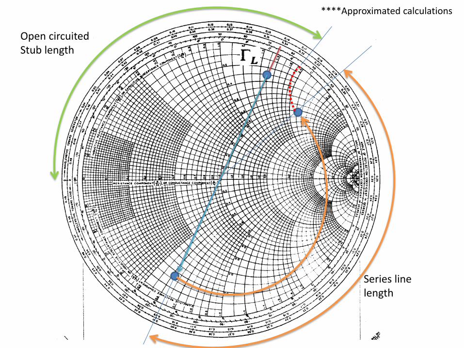
****Approximated calculations
Series line length
Open circuited Stub length
0.120×360o = 43.2o
0.206×360o = 74.16o
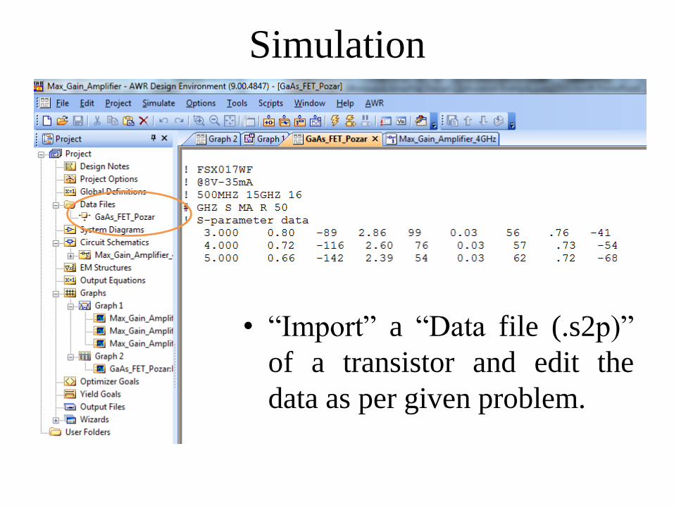
Simulation
• “Import” a “Data file (.s2p)”
of a transistor and edit the
data as per given problem.
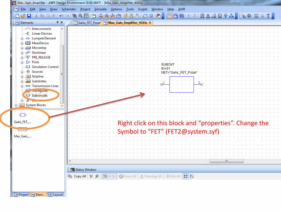
Right click on this block and “properties”. Change the Symbol to “FET” ([email protected])
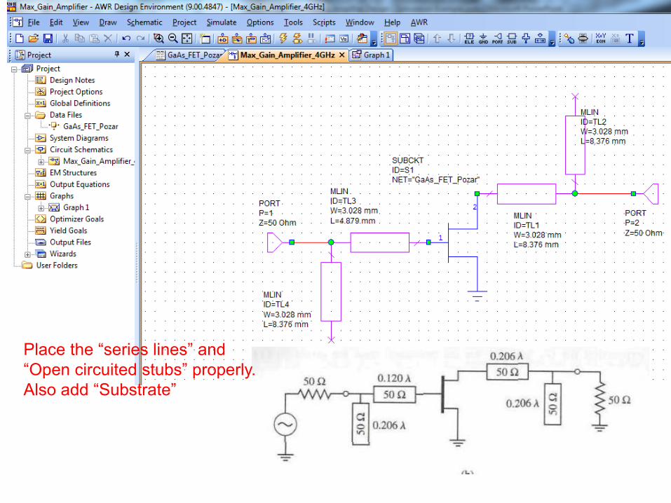
Place the “series lines” and
“Open circuited stubs” properly.
Also add “Substrate”
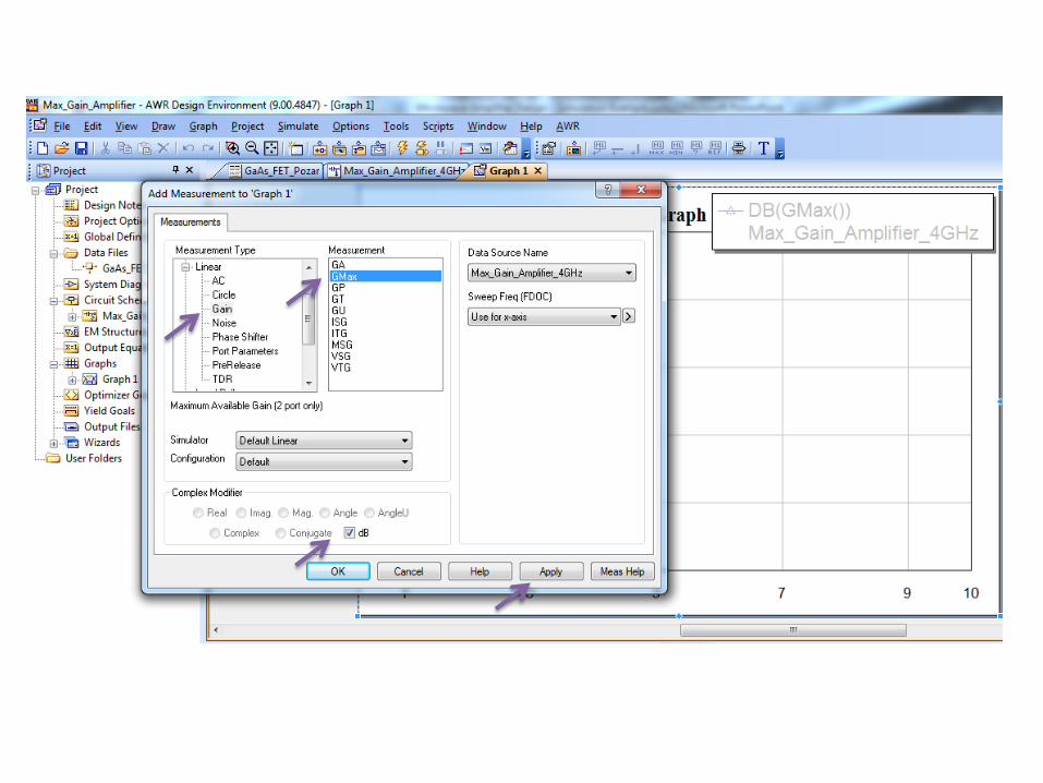
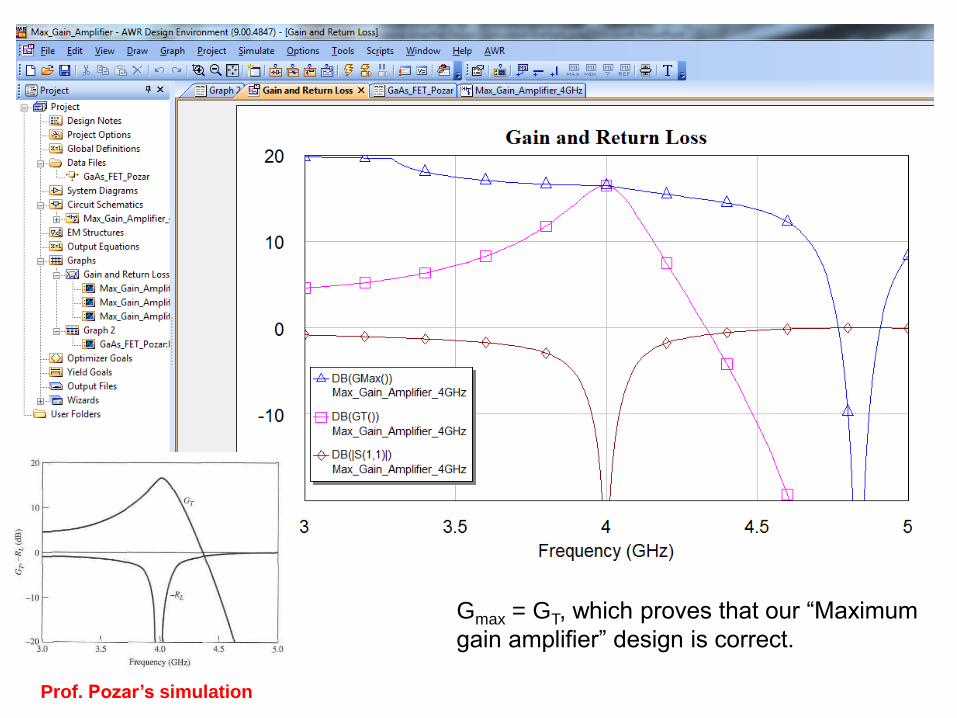
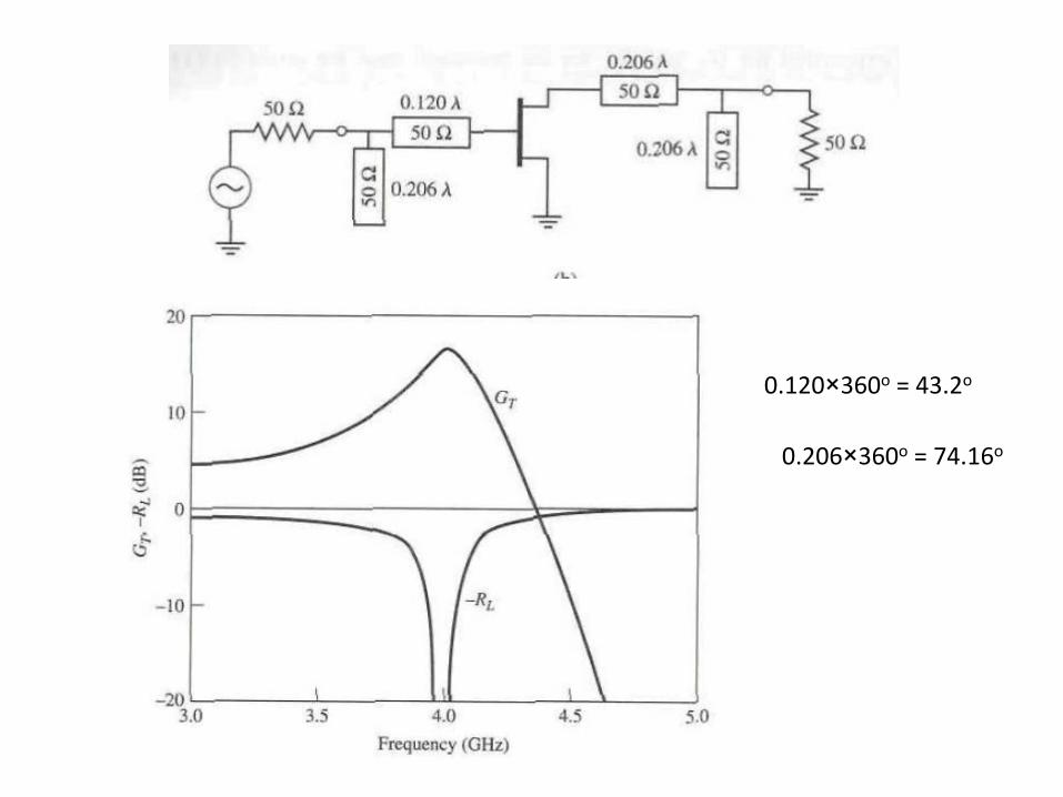
Prof. Pozar’s simulation
Gmax = GT, which proves that our “Maximum
gain amplifier” design is correct.


![RF Circuit Design - [Ch4-1] Microwave Transistor Amplifier](https://img.pdfslide.us/doc/110x75/55cc6094bb61eb9d338b474f/rf-circuit-design-ch4-1-microwave-transistor-amplifier.jpg)