Embed Size (px)
Citation preview

Joana Margarida Coimbra Lamas Pereira Correia
Licenciatura em Ciências da Engenharia Electroctécnica e deComputadores
Design of a Low-voltage CMOS RF Receiverfor Energy Harvesting Sensor Node
Dissertação para obtenção do Grau deMestre em Engenharia Electrotécnica e de Computadores
Orientador: Luís Augusto Bica Gomes de Oliveira,Professor Doutor, Universidade Nova de Lisboa
Júri:
Presidente: Professor Doutor Luís Filipe Figueira de Brito Palma
Arguente: Professor Doutor João Pedro Abreu de Oliveira
Vogal: Professor Doutor Fortunato Carlos Augusto Dualibe
Setembro, 2014


Design of a Low-voltage CMOS RF Receiver for Energy Harvesting SensorNode
Copyright c© Joana Margarida Coimbra Lamas Pereira Correia, Faculdade de Ciências eTecnologia, Universidade Nova de Lisboa
A Faculdade de Ciências e Tecnologia e a Universidade Nova de Lisboa têm o direito,perpétuo e sem limites geográficos, de arquivar e publicar esta dissertação através de ex-emplares impressos reproduzidos em papel ou de forma digital, ou por qualquer outromeio conhecido ou que venha a ser inventado, e de a divulgar através de repositórioscientíficos e de admitir a sua cópia e distribuição com objectivos educacionais ou de in-vestigação, não comerciais, desde que seja dado crédito ao autor e editor.
iii

iv

Dedicated to my lovely family

vi

Acknowledgements
The acknowledgment is a delicate section that requires special attention in the writing,mainly because it sums up the importance that some people have had in my academicpath. In case I forget to mention anyone important, I assure that I remember all the helpwas given to me.
I would like to express my appreciation to the Department of Electrical Engineeringof the Faculty of Sciences and Technologies for their excellent teaching standards, whichallow their students to acquire a broad knowledge and experience in various areas of thecourse under an enriching, friendly and knowledgeable guidance. To the teachers Prof.Luís Oliveira, Prof. João Pedro Oliveira and Prof. João Carlos Goes that have influencedmy final course path leading me to choose the area of electronics, in particular the RF cir-cuit design area, I want to thank for making electronics a captivating world. My advisor,Prof. Luís Oliveira, deserves a special mention, since he has always shown commitment,dedication and motivation in helping, which was a fundamental contribution during thiswork. I also would like to thank for the guidance and help of Prof. Fortunato Carlos Du-alibe from Faculté Polytechnique (UMOS) in Belgium, it was certainly essential in thecourse of my work.
I also wanted to express my appreciation for the friendly environment, the compan-ionship and helpful assistance of my colleagues from lab 3.5. I mention my boyfriendand working partner Nuno Mancelos, with whom I share fond memories since the firstday of college and in recent years have shared success and frustrations.
Finally, but not less important, I’m thankful to my family for their patience and per-severance over the years, the remarkable environment and good support they have pro-vided me. They were often deprived of my presence in various circumstances and yetcontinued to be my pillars in this sometimes frustrating path. With all this, I dedicatethis work to my family, knowing that without their support it would be more difficult.
vii

viii

Abstract
In this thesis a CMOS low-power and low-voltage RF receiver front-end is presented.The main objective is to design this RF receiver so that it can be powered by a piezoelectricenergy harvesting power source, included in a Wireless Sensor Node application. Forthis type of applications the major requirements are: the low-power and low-voltageoperation, the reduced area and cost and the simplicity of the architecture. The systemkey blocks are the LNA and the mixer, which are studied and optimized with greaterdetail, achieving a good linearity, a wideband operation and a reduced introduction ofnoise.
A wideband balun LNA with noise and distortion cancelling is designed to work ata 0.6 V supply voltage, in conjunction with a double-balanced passive mixer and sub-sequent TIA block. The passive mixer operates in current mode, allowing a minimalintroduction of voltage noise and a good linearity.
The receiver analog front-end has a total voltage conversion gain of 31.5 dB, a 0.1 -4.3 GHz bandwidth, an IIP3 value of -1.35 dBm, and a noise figure lower than 9 dB. Thetotal power consumption is 1.9 mW and the die area is 305x134.5 µm2, using a standard130 nm CMOS technology.
Keywords: CMOS RF receiver front-end; Low-power ; Low-voltage; Wideband balunLNA; Double-balanced passive Mixer; Wireless Sensor Networks.
ix

x

Resumo
Nesta tese é projectado o front-end analógico de um receptor RF CMOS com baixoconsumo e baixa tensão de alimentação. O receptor é projectado com o intuito de serincluído num nó sensor, alimentado por uma fonte de alimentação baseada em energyharvesting piezoeléctrico. Os requisitos mais importantes das aplicações wireless destetipo de nós sensores prendem-se com o baixo consumo e baixa tensão de alimentação,a redução de área e custo e a simplicidade da arquitectura. Os blocos mais importantesdo receptor são o LNA e o misturador, estudados e optimizados com maior detalhe deforma a alcançar boa linearidade e reduzida introdução de ruído.
A implementação do receptor inclui um LNA wideband balun, com capacidade decancelamento de ruído e distorção. O LNA é projectado para funcionar com uma ten-são de alimentação de 0,6 V, juntamente com um misturador passivo e amplificador detransimpedância. O misturador passivo opera em modo corrente, garantindo uma boalinearidade e uma reduzida introdução de ruído.
O ganho de conversão total do receptor é 31,5 dB, a sua largura de banda é 0,1 – 4,3GHz, o seu valor de IIP3 é -1,35 dBm, e a sua figura de ruído é inferior a 9 dB. O consumototal é de 1,9 mW e a área ocupada pelo circuito é 305x134.5 µm2, usando uma tecnologiastandard CMOS de 130 nm.
Palavras-chave: Receptor RF CMOS; Baixo consumo; Baixa tensão; LNA wideband ba-lun; Mixer passivo.
xi

xii

Contents
Abbreviations xix
1 Introduction 1
1.1 Background and Motivation . . . . . . . . . . . . . . . . . . . . . . . . . . . 1
1.2 Thesis Organization . . . . . . . . . . . . . . . . . . . . . . . . . . . . . . . . 2
1.3 Contributions . . . . . . . . . . . . . . . . . . . . . . . . . . . . . . . . . . . 3
2 Receiver architectures and RF Blocks 5
2.1 Receiver Architectures . . . . . . . . . . . . . . . . . . . . . . . . . . . . . . 5
2.1.1 Heterodyne Receiver . . . . . . . . . . . . . . . . . . . . . . . . . . . 6
2.1.2 Homodyne Receiver . . . . . . . . . . . . . . . . . . . . . . . . . . . 7
2.1.3 Low-IF Receiver . . . . . . . . . . . . . . . . . . . . . . . . . . . . . 8
2.2 Impedance matching . . . . . . . . . . . . . . . . . . . . . . . . . . . . . . . 10
2.3 Scattering parameters . . . . . . . . . . . . . . . . . . . . . . . . . . . . . . . 11
2.4 Noise . . . . . . . . . . . . . . . . . . . . . . . . . . . . . . . . . . . . . . . . 12
2.4.1 Thermal Noise . . . . . . . . . . . . . . . . . . . . . . . . . . . . . . 12
2.4.2 Flicker Noise . . . . . . . . . . . . . . . . . . . . . . . . . . . . . . . 13
2.4.3 Noise figure . . . . . . . . . . . . . . . . . . . . . . . . . . . . . . . . 13
2.5 Linearity . . . . . . . . . . . . . . . . . . . . . . . . . . . . . . . . . . . . . . 14
2.5.1 1 dB Compression Point . . . . . . . . . . . . . . . . . . . . . . . . . 15
2.5.2 Third-order Intercept Point . . . . . . . . . . . . . . . . . . . . . . . 16
2.6 Low Noise Amplifiers . . . . . . . . . . . . . . . . . . . . . . . . . . . . . . 16
2.6.1 Narrowband LNAs . . . . . . . . . . . . . . . . . . . . . . . . . . . . 17
2.6.2 Wideband LNAs . . . . . . . . . . . . . . . . . . . . . . . . . . . . . 18
2.7 Mixer . . . . . . . . . . . . . . . . . . . . . . . . . . . . . . . . . . . . . . . . 22
2.7.1 Active Mixer . . . . . . . . . . . . . . . . . . . . . . . . . . . . . . . 23
2.7.2 Passive Mixer . . . . . . . . . . . . . . . . . . . . . . . . . . . . . . . 25
xiii

3 Low-voltage receiver analog front-end 273.1 LNA . . . . . . . . . . . . . . . . . . . . . . . . . . . . . . . . . . . . . . . . 28
3.1.1 Gain . . . . . . . . . . . . . . . . . . . . . . . . . . . . . . . . . . . . 293.1.2 LNA input-impedance . . . . . . . . . . . . . . . . . . . . . . . . . . 313.1.3 Noise Factor . . . . . . . . . . . . . . . . . . . . . . . . . . . . . . . . 32
3.2 Receiver front-end circuit . . . . . . . . . . . . . . . . . . . . . . . . . . . . 403.2.1 Mixer . . . . . . . . . . . . . . . . . . . . . . . . . . . . . . . . . . . . 41
4 Receiver Implementation 434.1 Considerations, simulations and validation of the proposed circuit . . . . 43
4.1.1 LNA simulation results . . . . . . . . . . . . . . . . . . . . . . . . . 454.1.2 Receiver simulation results . . . . . . . . . . . . . . . . . . . . . . . 50
4.2 Layout design and post-layout simulations . . . . . . . . . . . . . . . . . . 564.3 Discussion . . . . . . . . . . . . . . . . . . . . . . . . . . . . . . . . . . . . . 61
5 Conclusion and Future Work 635.1 Conclusion . . . . . . . . . . . . . . . . . . . . . . . . . . . . . . . . . . . . . 635.2 Future Work . . . . . . . . . . . . . . . . . . . . . . . . . . . . . . . . . . . . 64
A Published Papers 69
xiv

List of Figures
2.1 Heterodyne Receiver . . . . . . . . . . . . . . . . . . . . . . . . . . . . . . . 62.2 Image rejection . . . . . . . . . . . . . . . . . . . . . . . . . . . . . . . . . . 62.3 Homodyne Receiver . . . . . . . . . . . . . . . . . . . . . . . . . . . . . . . 72.4 Image rejection architectures . . . . . . . . . . . . . . . . . . . . . . . . . . . 92.5 Diport with incident and reflected waves. . . . . . . . . . . . . . . . . . . . 112.6 Thermal noise represented in MOS transistors. . . . . . . . . . . . . . . . . 122.7 Noisy diport with gain A . . . . . . . . . . . . . . . . . . . . . . . . . . . . . 132.8 Definition of the 1 dB compression point . . . . . . . . . . . . . . . . . . . . 152.9 Definition of the third-order intercept point. . . . . . . . . . . . . . . . . . . 162.10 Degenerated common-source (CS) LNA topology . . . . . . . . . . . . . . 182.11 Common-gate LNA with resistive input matching . . . . . . . . . . . . . . 192.12 Wideband Balun LNA . . . . . . . . . . . . . . . . . . . . . . . . . . . . . . 202.13 MOSFET-only Wideband Balun LNA . . . . . . . . . . . . . . . . . . . . . . 222.14 Single Balanced Mixer . . . . . . . . . . . . . . . . . . . . . . . . . . . . . . 232.15 Gilbert Cell . . . . . . . . . . . . . . . . . . . . . . . . . . . . . . . . . . . . . 242.16 Passive Mixer using switch. . . . . . . . . . . . . . . . . . . . . . . . . . . . 25
3.1 Proposed LNA Circuit. . . . . . . . . . . . . . . . . . . . . . . . . . . . . . . 293.2 The small signal model for low frequencies of the LNA. . . . . . . . . . . . 303.3 The result of the LNA circuit’ approaches and approximations, including
some noise sources. . . . . . . . . . . . . . . . . . . . . . . . . . . . . . . . . 323.4 Common-gate (CG) model for all the noise contributions. . . . . . . . . . . 343.5 The approximate small signal model of CG circuit. . . . . . . . . . . . . . . 363.6 Common-source (CS) model for all the noise contributions. . . . . . . . . . 373.7 Complete Receiver Circuit. . . . . . . . . . . . . . . . . . . . . . . . . . . . . 413.8 Mixer architecture. . . . . . . . . . . . . . . . . . . . . . . . . . . . . . . . . 42
4.1 The LNA’s current mirror structure. . . . . . . . . . . . . . . . . . . . . . . 454.2 LNA Gain and Bandwidth. . . . . . . . . . . . . . . . . . . . . . . . . . . . 46
xv

4.3 LNA input impedance. . . . . . . . . . . . . . . . . . . . . . . . . . . . . . . 474.4 LNA IIP3. . . . . . . . . . . . . . . . . . . . . . . . . . . . . . . . . . . . . . . 484.5 LNA noise summary. . . . . . . . . . . . . . . . . . . . . . . . . . . . . . . . 484.6 LNA Noise Figure. . . . . . . . . . . . . . . . . . . . . . . . . . . . . . . . . 494.7 LNA output current. . . . . . . . . . . . . . . . . . . . . . . . . . . . . . . . 514.8 Receiver’s noise figure. . . . . . . . . . . . . . . . . . . . . . . . . . . . . . . 514.9 Mixer input impedance. . . . . . . . . . . . . . . . . . . . . . . . . . . . . . 524.10 Receiver input impedance. . . . . . . . . . . . . . . . . . . . . . . . . . . . . 534.11 IIP3 simulation. . . . . . . . . . . . . . . . . . . . . . . . . . . . . . . . . . . 544.12 Output signals of the TIA. . . . . . . . . . . . . . . . . . . . . . . . . . . . . 544.13 Differential output signal of the TIA. . . . . . . . . . . . . . . . . . . . . . . 554.14 The proposed circuit layout. . . . . . . . . . . . . . . . . . . . . . . . . . . . 564.15 The receiver components identification of the layout design. . . . . . . . . 574.16 The output current of the LNA. . . . . . . . . . . . . . . . . . . . . . . . . . 584.17 Receiver’s output signals. . . . . . . . . . . . . . . . . . . . . . . . . . . . . 594.18 Receiver’s noise figure. . . . . . . . . . . . . . . . . . . . . . . . . . . . . . . 60
xvi

List of Tables
4.1 Initial Dimensions of the Transistors. . . . . . . . . . . . . . . . . . . . . . . 444.2 Resistor and Capacitor dimensions. . . . . . . . . . . . . . . . . . . . . . . . 454.3 The theoretical and schematic results of the LNA. . . . . . . . . . . . . . . 494.4 Comparison with State-of-the-art LNAS. . . . . . . . . . . . . . . . . . . . . 504.5 Optimized transistors dimensions. . . . . . . . . . . . . . . . . . . . . . . . 504.6 Final receiver simulation results. . . . . . . . . . . . . . . . . . . . . . . . . 554.7 The layout design parameters. . . . . . . . . . . . . . . . . . . . . . . . . . . 584.8 The schematic and layout simulations results. . . . . . . . . . . . . . . . . . 614.9 Comparison of WSN receivers. . . . . . . . . . . . . . . . . . . . . . . . . . 62
xvii

xviii

Abbreviations
AC Alternating Current
ADC Analog to Digital Converter
BER Bit Error Rate
BW BandWidth
CG Common-Gate
CL Conversional Loss
CMOS Complementary Metal-Oxide-Semicondutor
CS Common-Source
DC Direct Current
DRC Design Rule Check
DTMOS Dynamic Threshold MOS
FET Field Effect Transistor
FoM Figure of Merit
FSK Frequency Shift Keying
HR High-Resistance
IC Integrated Circuit
IF Intermediate Frequency
IIP Input Reference Intercept Point
KVL Kirchhoff’s Voltage Law
LDO Low-DropOut
LNA Low Noise Amplifier
xix

LO Local Oscillator
LPE Layout Parameter Extraction
LPF Low-Pass Filter
LVS Layout Versus Shematic
MIM Metal-Insulator-Metal
MOSFET Metal-Oxide-Semiconductor Field-Effect Transistor
NEF Noise Excess Factor
NF Noise Figure
NMOS Nchannel Metal-Oxide-Semicondutor
OOK On/Off Keying
OTA Operational Transconductance Amplifier
PMOS Pchannel Metal-Oxide-Semicondutor
PSSR Power Supply Rejection Ratio
PWM Pulse Width Modulation
Q Quality factor
RF Radio Frequency
RMS Root-mean-square
SC Switched Capacitor
SNR Signal-to-Noise Ratio
SoC System-on-Chip
TIA TransImpedance Amplifier
VCVS Voltage Controlled Current Source
VDD Value-Driven Design
WSAN Wireless Sensor Actuator Nodes
WSN Wireless Sensor Network
xx

1Introduction
1.1 Background and Motivation
Integrated circuits (ICs) have been experiencing a remarkable progress in terms of de-vice size reduction, range of operation frequencies and overall performance. The mostinfluential factor was the advent of the field-effect transistor (FET), which operates asa conducting semiconductor channel, responsible for the flow of charge carriers in thechannel. The FET is a voltage-controlled device with four terminals: the source (S), thedrain (D), the gate (G) and the bulk (B). The channel is formed between the terminals Sand D. While, the terminal G modulates the channel conductivity, controlling the densityof charges carriers in the channel. The terminal B allows a connecting to the device’ssubstrate [1–3].
The dominant type of transistor in today’s integrated circuits is the metal-oxide-semiconductor field-effect transistor (MOSFET). These transistors offer a dense integra-tion of the circuits in terms of the number of transistors per unit area of silicon substrate,a low cost of fabrication, an improvement in the overall performance and a low powerconsumption. The CMOS technology is growing towards to integration of digital blocks,analog and RF circuits on a single chip to implement the so called system-on-chip (SoC)solutions [1–3].
So, in order to originate a Wireless Sensor Networks (WSNs), several individual sen-sor nodes, Wireless Sensor Actuator Nodes (WSAN), are energetically autonomous andwirelessly interconnected. These WSANs share information through the communicationchannel, where the commands are transmitted through their radio transceivers by mod-ulating the different characteristics of the radio frequency (RF) signal. The transceiversare responsible for connecting individual nodes of the network because of their function
1

1. INTRODUCTION 1.2. Thesis Organization
of receiving and transmitting information, allowing the WSN to be formed. The mainblocks of the transceiver are the transmitter and the receiver.
In the transmitter side, the information suffers a process called modulation, wherethe signal goes through several changes as it passes from baseband to higher frequency.This process makes the wave carry more information and also helps reducing the size ofthe antennas. In addition, other important matter for the wireless sensor is in the waythe signal propagates by the communication channel. This channel causes attenuation inthe transmitted RF signal during propagation. The attenuated RF signal must be ampli-fied by the receiver, which is also responsible for filtering eventual interferences. Afteramplification, the receiver converts the input signal to baseband, in order to demodulateand access the original information [4].
Moreover, the wireless sensor node installation depends on their characteristics andcommunication range, which influences the total circuit area. Also, these nodes shouldbe energetically autonomous and individually powered. A common solution to makethese nodes energetically autonomous is the use of batteries. Although it guaranteesthe node’s wireless operation, this type of power solution has limited energy supply,requiring periodical maintenance.
In an ideal situation, the wireless sensor node should operate with low power con-sumption, where the node is self-sufficient in terms of energy, or self-powered. The pos-sibility of making the node autonomous, maintenance-free and unattended is feasibleby energy harvesting. This type of energy solution makes use of residual energy that ispresent in the different enviroments where the WSANs are installed. This residual energyis present in different forms and has numerous sources, mainly solar, thermal gradient,electromagnetic or electromechanical. So the energy harvesting faces the challenge ofscavenging and converting enough residual energy to power different circuits [5].
The scope of this work is to design and implement, through CMOS technology, alow power consumption front-end RF receiver, enabling to be powered by an energyharvesting power supply. The included RF receiver blocks are the LNA, mixer, localoscillator (LO) and the transimpedance amplifier (TIA). However, the main focus is overthe new implementation of LNA and mixer combination, where the signals are treated incurrent mode. This approach plays an important role in the present work, which verifiesif the considerations made on each block are sufficient to validate the main objectives.
1.2 Thesis Organization
Besides the introductory chapter, this thesis has been organized in five chapters as willbe presented:
In chapter 2, the state-of-the-art is presented, which means the information is gath-ered about the architectures, devices, processes and techniques that are applied to RF re-ceivers front-end. Some RF receiver topologies and characteristics are briefly described.Also, some basic concepts are introduced, the scattering parameters, the noise and the
2

1. INTRODUCTION 1.3. Contributions
linearity. The LNA and mixer topologies are presented and discussed, making a distinc-tion between narrowband and wideband LNAs and active and passive mixers.
Chapter 3 presents the main attributes of the LNA, mixer and complete receiver ofthis work, including the analysis of the most relevant equation for each of them. The maincharacteristics of the LNA module are specified, and the changes made to the originalLNA are presented. The deduction of the main equations regarding the LNA is given,namely the differential voltage gain, the input impedance and noise factor. The mixerdesign includes the development strategies that were considered in order to enable thismodule to perform the mixing operation in current mode. At the end of the chapter, thedesign of the complete receiver circuit is demonstrated, including the deduction of theconversion gain equation and some important characteristics.
Chapter 4 presents the dimensioning of the proposed receiver circuit, as well as theschematic and post-layout simulations. The implementation procedures used to dimen-sion the receiver circuit before the layout are summarized and the initial values and pa-rameters are given. Also, this chapter gives focus to the LNA block because of its im-portance and influence on the final results of the entire proposed circuit. The theoreticalexpressions and characteristics obtained in the previous chapter are combined and vali-dated through simulation results and thus a comparison with state-of-art LNAs is made.Before the circuit layout, the transistor dimensions are optimized for the receiver circuit,with its behaviour and performance analysed through the simulation results. Then, thecircuit layout is produced, and post-layout simulations are performed, enabling the com-parison of the schematic and layout simulation results. Finally, the discussion of resultsis made and it is verified if the circuit satisfies the requirements for the target application.
Chapter 5 gives the general conclusions and further research suggestions.
1.3 Contributions
The main contributions of this thesis are as follows.
There are several low voltage techniques responsible for the functioning of the circuitsat low voltage, lower than 0.7 V. The technique explored in this thesis was the dynamicthreshold MOS (DTMOS), which is applied on the first block of the RF receiver front-end and takes into account the transistors choice in which the technique should be used.However, before using this technique of low voltage in the proposed receiver of the the-sis, it was explored and studied in a two-stages rail-to-rail input/output, constant Gmamplifier. This work was submitted to the DoCEIS, 5th Doctoral Conference on Com-puting, Electrical and Industrial Systems, entitled "Stability improvements in a Rail-to-RailInput/Output, constantGm Operational Amplifier, at 0.4 V operation, using the low-voltage DT-MOS technique" [6].
Another article was submitted to DoCEIS, 5th Doctoral Conference on Computing,Electrical and Industrial Systems, with the title "Piezoelectric energy harvester for a CMOS
3

1. INTRODUCTION 1.3. Contributions
wireless sensor" [7], where the concept of energy between wireless sensor nodes and en-ergy harvesting is explored. Therefore, this technique of energy harvesting is promis-ing in collecting the residual energy present in diversified environments and forms, giv-ing special emphasis to the piezoelectric energy harvesting. Also, it presents a range ofWSAN with different functionalities, characteristics and estimated power consumptionlevels. A study and experimental evaluation of a flexible piezoelectric material is madeto validate the use of a piezoelectric harvester in a CMOS WSAN. This work has leadto the conclusion of the requirements for the energy harvesting solution in the proposedreceiver of this thesis, which are low-voltage supply and low-power consumption.
The RF receiver design has a wideband balun LNA with noise cancelling and a pas-sive mixer. The combination of these two blocks treats the signals in current mode, en-abled by the local oscillator (LO). The TIA is placed after the mixer module, and is re-sponsible for converting the current signal to a voltage signal. The proposed receivercircuit is designed in 130 nm CMOS technology and its requirements present a suitablesolution for the target application. This work also presents the theoretical analysis, thekey parameters, some characteristics and simulations results. This work was submittedto the MIXDES, 21th International Conference (2014), entitled "A Low-Voltage LNA andCurrent Mode Mixer Design for Energy Harvesting Sensor Node" [8].
An extended version, entitled "Co-design of a Low-power RF Receiver and PiezoelectricEnergy Harvesting Power Supply for a Wireless Sensor Node" was published in the Interna-tional Journal of Microelectronics and Computer Science. In the extended version, theprevious work of a low-voltage RF CMOS receiver front-end is presented in conjunctionwith a piezoelectric energy harvesting power circuit for a wireless sensor node solution.The energy harvesting power circuit is composed by an active full-bridge cross-coupledrectifier and a low-dropout (LDO) regulator [9].
4

2Receiver architectures and RF Blocks
In this chapter, the supply and support for theoretical analysis and design of front-end RFcircuits, mainly in the receiver’s side, is presented. In section 2.1, an overview of the threemain conventional receiver architectures, namely, heterodyne, homodyne and low-IF, isoffered, including some advantages and disadvantages, characteristics and conclusions.
Section 2.2 presents the importance of impedance matching on RF circuits and thenecessary requirements for maximize the energy transferred between blocks. The section2.3 focus in the scattering parameters, which relates the electromagnetic waves incidentand reflected . In section 2.4, a common noise sources overview is given, namely, ther-mal noise, flicker noise and noise figure. The section 2.5 gives an overall notion of themost important characteristics of linearity measurement and presents the 1 db linearitycompression point and third-order intermodulation product.
The typical structures and important front-end blocks are introduced in sections 2.6and 2.7. In the case of section 2.6, the main focus is given in the narrowband and wide-band LNAs topologies. While, in section 2.7 is emphasized the differences and character-istics of active and passive mixers.
2.1 Receiver Architectures
To understand the rules that prevail when designing receiver for WSN, was chosen deepenthe knowledge about these structures. The receiver’s architectures are used to fulfil pro-cesses such as amplification and down-conversion of the signal. Also nowadays, theirrequirements are more demanding in terms of interference rejection, band selectivity, fullintegration and dimensions. This section emphasizes three receiver types, describes someof their characteristics, advantages and disadvantages.
5

2. RECEIVER ARCHITECTURES AND RF BLOCKS 2.1. Receiver Architectures
2.1.1 Heterodyne Receiver
The Wireless Sensor Networks (WSNs) have used for a long time heterodyne receivertopology, shown in Fig. 2.1. The RF signal from the transmitter is received by the antennaand filtered through a baseband filter, which removes the unwanted frequencies. Also,the received signal is weak and needs to be amplified by the Low Noise Amplifier (LNA).Then, other filter is applied to the signal, the image rejection filter, his function is attenu-ate signals at image band frequencies from the LNA. The down-converted process placesthe signal frequency to an intermediate frequency (IF), which is done through the signalmultiplier (mixer) that is applied by the output signal of the Local Oscillator (LO). At themultiplier output is used another baseband filter, the channel selection filter, that isolatesthe desired signal from the others adjacent IF signals from nearby channels. In this re-ceiver topology, the blocks responsible for the demodulation process are the Analog toDigital Converter (ADC) and the digital signal processor.
RF Band-
Pass
Filter
LNAImage
Rejection
Filter
VCO
Channel
Selection
Filter
ADC and
DSPfrf
flo
fif Data
Figure 2.1: Heterodyne Receiver
ωloωrf ωωim
ωif ωif
Imagem
Channel
ωloωrf ωωim
ωif ωif
Imagem
Channel
0ωif
Image rejection
filter
Figure 2.2: Image rejection
The frequency image problem occurs when the input mixer has a resultant signalcalled signal image, which after the multiplications generates two signals at the outputmixer. Unfortunately, one of them coincides with the intermediate frequency (IF) causingan overlap in the interest signal, which makes impossible separate both. That’s whyis necessary to have before the multiplier a filter called image rejection filter, show in
6

2. RECEIVER ARCHITECTURES AND RF BLOCKS 2.1. Receiver Architectures
Fig. 2.2.
A further disadvantage associated with the choice of IF frequency value is caused byits increase. With the highest IF frequency becomes easier to develop the filter that rejectsthe image (image rejection filter), because the image became farther from the desiredfrequency. On the other hand, this architecture has a compromise between the qualityfactor (Q) and the Intermediate Frequency (IF). What makes the specifications for thechannel selection filter more difficult to realize on-chip [4, 10, 11].
2.1.2 Homodyne Receiver
The homodyne receiver (Fig. 2.3) known by other names such as direct conversion andZero-IF receiver, converts the Radio Frequency (RF) signal to baseband. This conversionis done using a Local Oscillator (LO) with the same frequency as the RF signal. This re-ceiver type has advantages compared with heterodyne receiver. First, the inexistence ofimage signal makes unnecessary the use of the image filter rejection. Second, the filterthat performs the channel selection is done through a Low-Pass Filter (LPF), making thedesign and implementation simpler. Finally, it allows the possibility of complete integra-tion of the receiver on-chip.
RF Band-
Pass Filter
(BPF)LNA
ADC and
DSP
VCO
flo
90º
flo
Low-Pass
Filter
(LPF)
Low-Pass
Filter
(LPF)
ADC and
DSP
frf
I
Q
Figure 2.3: Homodyne Receiver
The direct converter architecture has some downsides:
• Flicker Noise - The Flicker noise can significantly corrupt the low frequency of thebaseband signal, which is a big problem in CMOS implementations (1/f corner atlow frequency).
• LO leakage - Local Oscillator (LO) leakage happens when the insulation is imper-fect between the LO port and the input ports of the LNA and mixer. This leakage
7

2. RECEIVER ARCHITECTURES AND RF BLOCKS 2.1. Receiver Architectures
signal appears when the LNA and mixer’s inputs are mixed with the signal comingfrom LO, producing an unwanted DC component at the mixer output, which cancause the saturation of the following blocks. To minimize this effect is necessary theuse of differential LO and mixer outputs to cancel common mode components.
• DC offsets – Since the down-converted band extends down to zero frequency, anyoffset voltage can corrupt the signal and saturate the receiver’s baseband outputstages. Hence, DC offset removal or cancellation is required in direct-conversionreceivers.
• Quadrature error and mismatches - Quadrature error and mismatches betweenthe amplitudes of the I and Q signals results in the corruption of the received signalconstellation, which increase the Bit Error Rate (BER). The ideal baseband signalsshould have similar amplitude and phase difference of 90 degrees.
• Intermodulation - In the intermodulation, the receivers must have a high IIP2
(second-order intermodulation intercept point) to avoid producing DC offset. [4,10, 11]
2.1.3 Low-IF Receiver
The previous two architectures were useful once, but the combination of both advantagesgave the Low-IF receiver. This receptor cancels the image frequency by using special mix-ing circuits that allows the selection of a low intermediate frequency. The problem thatarises in the homodyne receiver is avoided by relaxing the quality factor of the channelselection filter, in particular the flicker noise that affects baseband signals.
The technique for cancellation of image signal is used to avoid the use of image re-jection filter which is one of the problems associated with the heterodyne receiver. Can-cellation of image is done through two architectures: Hartley and Weaver. This methodof image rejection is achieved using the quadrature architectures, in which the image issuppressed by its negative replica.
The Hartley architecture has the block diagram represented in Fig. 2.4(a). The idea isto process the RF signal after the Low-Pass Filter (LPF) and combine both outputs into asingle one. Assuming that the RF signal is represented by the expression 2.1, then afterthe filtering process the expressions are 2.2 and 2.3, respectively.
xRF (t) = VRF cos(ωRF t) + VIMcos(ωIM t) (2.1)
yA(t) =VRF
2sin[(ωLO − ωRF )t] +
VIM2sin[(ωLO − ωIM )t] (2.2)
8

2. RECEIVER ARCHITECTURES AND RF BLOCKS 2.1. Receiver Architectures
yB(t) =VRF
2cos[(ωLO − ωRF )t] +
VIM2cos[(ωLO − ωIM )t] (2.3)
Since sin(θ - π2 )= -cos(θ), after a 90o
shift, the signal at C is,
yC(t) =VRF
2cos[(ωRF − ωLO)t]− VIM
2cos[(ωLO − ωIM )t] (2.4)
RF Band-
Pass Filter
(BPF)LNA
LO
Sin(ωlot)
- 90º
Low-Pass
Filter
(LPF)
Low-Pass
Filter
(LPF)
xRF
Cos(ωlot)
A
B
90º
IF
C
(a) Hartley
RF Band-
Pass Filter
(BPF)LNA
LO1
Sin(ωlo1t)
90º
Low-Pass
Filter
(LPF)
Low-Pass
Filter
(LPF)
xRF
Cos(ωlo1t)
IF
LO2
Sin(ωlo2t)
90º
Cos(ωlo2t)
(b) Weaver
Figure 2.4: Image rejection architectures
Finally, by adding the expressions 2.3 and 2.4 the wanted signal is recovered and theimage is suppressed.
Lastly, the Weaver architecture, represented in Fig. 2.4(b),has similar results but ituses a second mixer stage at the intermediate frequency. Both architectures enabled thecancellation of image signal, which depend on the precision of the oscillators to producequadrature signals. However, both solutions are susceptible to quadrature errors result-ing phase and gain imbalances.
9

2. RECEIVER ARCHITECTURES AND RF BLOCKS 2.2. Impedance matching
In conclusion, the Low-IF receiver becomes more flexible compared to the previoustopologies [11].
2.2 Impedance matching
The transmission line is one of the main focus of a complex structure of an RF circuit.The signal that goes through the transmission line has to ensure that the impedance ofoutput block is equal to the characteristic impedance of the next block. If is verified themismatch of the impedances this originates a reflected voltage and current which reducesthe transmitted energy between blocks. The voltage and current at any point along theline may be expressed as:
V (z) = Vie−γz + Vre
γz (2.5)
I(z) = Iie−γz − Ireγz (2.6)
where the term e−γz represents the wave propagation in the z+ direction and eγz
in the z− direction. Also the terms Vi, Vr, Ii and Ir are the amplitudes voltages andcurrents of the incident and reflected waves, respectively. The expression γ representsthe propagation constant with the resistance R that represents the conductor loss and theconductance G, which is the dielectric loss between the two conductors.
γ =√
(R+ jωL)(G+ jωC) (2.7)
The characteristic impedance of the transmission line is expressed by using the Ohm’slaw and the equations 2.5 and 2.6:
Z0 =ViIi
=VrIr
=R+ jωL
γ(2.8)
While the load impedance is expressed as follows:
ZL =V (0)
I(0)=Vi + VrVi − Vr
Z0 (2.9)
The reflection coefficient is the ratio between the normalized reflection and the inci-dent waves of load impedance at the end of the transmission line:
Γ =ZL − Z0
ZL + Z0(2.10)
The reflection coefficient is inexistent (rL = 0) when the characteristic impedance isequal to the load impedance (ZL = Z0)), which maximizes the energy transferred be-tween the blocks. As an example, for the RF systems the impedance matching is im-portant because of the antenna and the first block, usually LNA, must coincide with animpedance of 50 Ω [12].
10

2. RECEIVER ARCHITECTURES AND RF BLOCKS 2.3. Scattering parameters
2.3 Scattering parameters
The traditional system characterization is done through two ways. At low frequencies,the system uses measurements of open and short-circuits to determine the admittanceand hybrid parameters. While, at high frequencies, the methods used by the system atlow frequencies are not possible because of the port voltages or currents measurementsthat include magnitude and phase of the travelling waves. Therefore, the s-parametersalso called as scattering parameters, are used to characterize the inputs and outputsvariables of systems working at high frequencies, in order to auxiliary the adaptationof impedance matching, to provide the maximum value gain, the input and the outputimpedance and even possible instabilities. The scattering parameters that relate the in-put and output of electromagnetic waves, are shown in the Fig. 2.5 below as a1, b1, b2 anda2, when the system is viewed as a diport. These waves are generated by the input andoutput ports from the diport who represents the system.
a1
b1 a2
b2Diport
Figure 2.5: Diport with incident and reflected waves.
The s-parameters relate the electromagnetic waves as follows:
S11 =b1a1
(com a2 = 0) (2.11)
S12 =b1a2
(com a1 = 0) (2.12)
S21 =b2a1
(com a2 = 0) (2.13)
S22 =b2a2
(com a1 = 0) (2.14)
Therefore, the s-parameters have the following designation: the S11 is the input re-flection coefficient, while S21 is the transmission gain since relates an output wave (b2)to an input wave (a1). The S12 corresponds to the reverse transmission gain consideringthe input and output diport swapped, which means the electromagnetic wave that enterson the diport is a2 and not a1. Finally, the last s-parameter is S22, the output reflectioncoefficient.
The calculations of the s-parameters are made relating the terms of incident and re-flected voltages of electromagnetic waves a1, a2, b1 and b2, , enabling the development of
11

2. RECEIVER ARCHITECTURES AND RF BLOCKS 2.4. Noise
design circuit without internal detailed knowledge [12].
2.4 Noise
Noise is one of the most important parameters in analog design more precisely, in RFcircuits. This parameter is responsible for the degradation of circuit performance and itsappearance is caused by external interference or by the intrinsic nature of the circuit ma-terials. Due to its random behaviour and difficult prediction which mean that unwantedsignals are added to the desired signal, therefore it is necessary to find an approach tominimize this effect. This section will describe the common sources of noise present inCMOS technologies [13].
2.4.1 Thermal Noise
The thermal noise depends on the temperature that causes variation in the resulting cur-rent, which is generated by the random motion of electrons that pass through the ohmicresistance devices. As the temperature of the device increases, the random motion of themolecules increase, and so does the corresponding noise level; therefore, it is known asthermal noise. The average noise power remains nearly independent of frequency andcan be adequately approximated as
V 2n = 4KTR∆f (2.15)
where the absolute temperature T (in Kelvin), the Boltzmann constant K and thebandwidth of the system is ∆f . This can be quantified by a series voltage source us-ing the Thevenin equivalent, or by a parallel current using the Norton equivalent [3,13].
The thermal noise also appears in MOS transistors due to the carrier motion throughthe channel and is represented as shown in Fig. 2.6 by a parallel current source to theconduction channel.
In2
Figure 2.6: Thermal noise represented in MOS transistors.
The equations of thermal noise are defined depending on the region of the transistor.If the transistor is operating in the triode region (gd0 >> gm), the gd0 is the drain-sourceconductance for Vds = 0 and γ is the Noise Excess Factor (NEF). If it is in the saturation
12

2. RECEIVER ARCHITECTURES AND RF BLOCKS 2.4. Noise
region (gm >> gd0), the transistor operates in a long channel with the value γ = 2/3 [2,13].
I2n = 4KTγgm∆f (2.16)
2.4.2 Flicker Noise
The flicker noise or 1/f noise is a low-frequency noise resulted by the surface and gateeffects in the semi-conductor material, which means by the interface between the gateoxide (SiO2) and the silicon substrate (Si). The measured noise power in MOSFET deviceshas a dependence on the gate bias and the oxide thickness. The flicker noise equation thatis represented in 2.17,has parameters like the process dependent constant (kf ), the gateoxide capacitance per unit area (cox), the width (W) and length (L) of the transistor.
Vnf2 =kf
coxWLfαf(2.17)
This type of noise becomes more crucial to provide enough dynamic range and bettercircuit performance [2, 14].
2.4.3 Noise figure
One of the most important parameter in an RF circuit is the noise factor (F), or the noisefigure (NF), when calculated in dB. The noise factor represents the ratio of the total outputnoise and the input noise of the system. When is modelled as a diport, as represented inFig. 2.7, in this case, the measurements are relative to the total noise power between theoutput, input and its gain for each frequency.
Diport VS
RSIi Io
RLVoVi
Figure 2.7: Noisy diport with gain A
The noise factor can be expressed by:
F =No
A2Ni(2.18)
The noise factor can also be expressed as the power ratio between the desired signalto the total noise (unwanted signal), which is done through the ratio of signal-to-noise
13

2. RECEIVER ARCHITECTURES AND RF BLOCKS 2.5. Linearity
ratio (SNR) at the input and at the output. This expression demonstrates how much theSNR degrades as the signal passes through the system [13].
F =SNRinSNRout
(2.19)
2.5 Linearity
The measurement of the RF system linearity is really important to understand the impactof nonlinear devices have in the output signal. The linearity can be characterized by the1 dB compression point and by third-order intermodulation product.
The RF circuits are constituted by devices with nonlinear characteristics, such as MOStransistors, which in addition to this feature they are also memoryless, time invariant andcan be represented by the Taylor series:
y(t) = a0 + a1x(t) + a2x2(t) + ...+ anx
n(t) (2.20)
Suppose a sinusoidal 2.21 as an input signal:
x(t) = Acos(ωt) (2.21)
The system response can be expressed by:
y(t) = a0 + a1Acos(ωt) + a2A2cos2(ωt) + a3A
3cos3(ωt) (2.22)
Nonlinear devices produce the same harmonic as the order of their nonlinearitieswith multiples of the fundamental frequency (nω). The order coefficients have differenteffects on the nonlinear devices. When is odd, the order coefficients have impact onthe amplitude of the fundamental frequency, while in case of even order coefficients theimpact is on the DC component.
In the case where two sinusoidal signals are applied at the nonlinear device inputwith different fundamental frequencies,
x(t) = Acos(ω1t) +Bcos(ω2t) (2.23)
The intermodulation products emerge at the output signal as it is expressed in 2.24,which illustrates the operations between the input signal frequencies and their multiplesof the fundamental frequency. The nonlinearity of order 3 (IM3) is an example that the in-termodulation product appearing in the frequency band of interest and can’t be removedby a filter [1, 4, 13].
14

2. RECEIVER ARCHITECTURES AND RF BLOCKS 2.5. Linearity
The intermodulation products are generated at the output signal, given by:
y(t) = a0 + a1
(Acos(ω1t) +Bcos(ω2t)
)+
a2
[A2
2(1 + cos(2ω1t)) +
B2
2(1 + cos(2ω2t)) +AB(cos(ω1 + ω2)t) + cos((ω1 − ω2)t))
]+
a3
[(3
4A3 +
3
2AB2)cos(ω1t)) + (
3
4B3 +
3
2BA2)cos(ω2t)) +
3
4A2B(cos(2ω1 + ω2)t)+
cos(2ω1 − ω2)t)) +3
4B2A(cos(2ω2 + ω1)t) + cos(2ω2 − ω1)t)) +
3
4A3cos(3ω1t)+
3
4B3cos(3ω2t)
](2.24)
2.5.1 1 dB Compression Point
The 1 dB compression point is a linearity measure of the circuit and it’s also known asgain compression or saturation. Their effect takes into account the gain of the circuit, therelation between the output and input power, by checking its linearity measure. Throughthe Fig. 2.8 can be seen the ideal linear characteristic with the real characteristic of the cir-cuit over a limited range. However, its real characteristic begins to saturate, resulting inreduced gain. To check the circuit’s linearity measure, the compression point 1 dB is de-fined through the difference of 1 dB from the ideal linear characteristic, this happens dueto the increase of input power which makes the higher order harmonics more notable [1].
1 dB
1 dB
compression
point, P1dB
Pin [dB]
Pout [dB]
OP1dB
IP1dB
Figure 2.8: Definition of the 1 dB compression point
15
2. RECEIVER ARCHITECTURES AND RF BLOCKS 2.6. Low Noise Amplifiers
2.5.2 Third-order Intercept Point
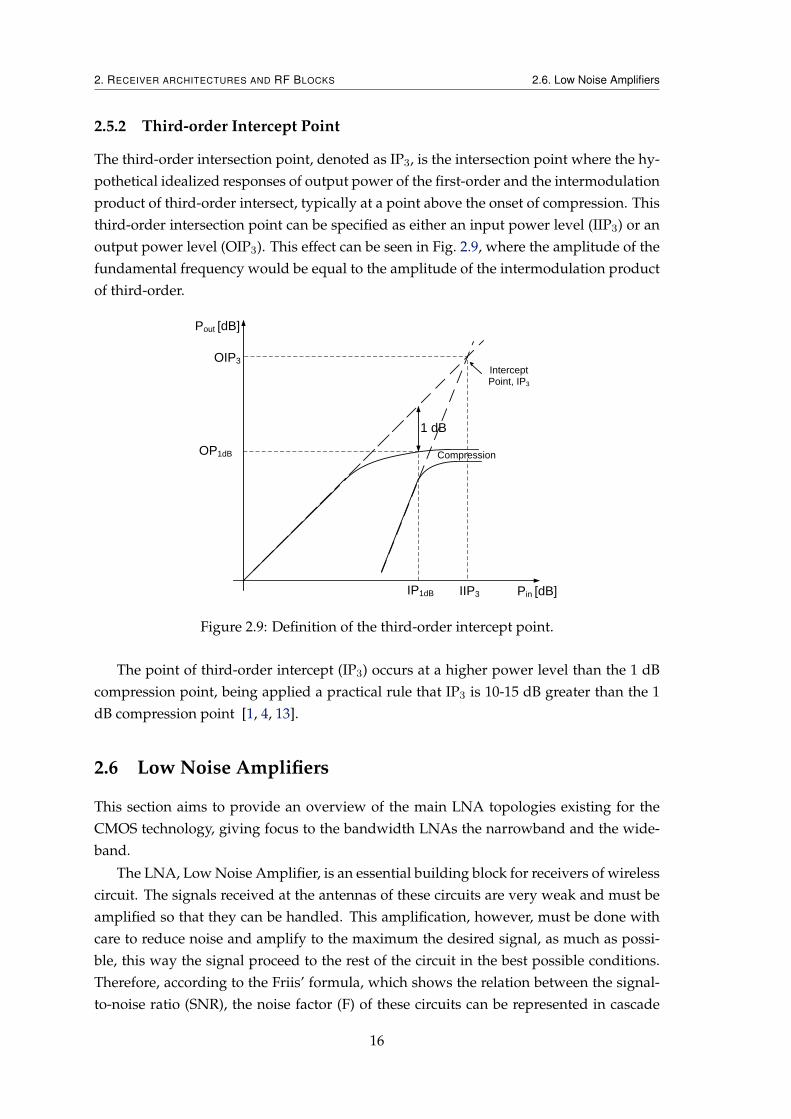
The third-order intersection point, denoted as IP3, is the intersection point where the hy-pothetical idealized responses of output power of the first-order and the intermodulationproduct of third-order intersect, typically at a point above the onset of compression. Thisthird-order intersection point can be specified as either an input power level (IIP3) or anoutput power level (OIP3). This effect can be seen in Fig. 2.9, where the amplitude of thefundamental frequency would be equal to the amplitude of the intermodulation productof third-order.
1 dB
Pin [dB]
Pout [dB]
OP1dB
IP1dB
OIP3
IIP3
Intercept Point, IP3
Compression
Figure 2.9: Definition of the third-order intercept point.
The point of third-order intercept (IP3) occurs at a higher power level than the 1 dBcompression point, being applied a practical rule that IP3 is 10-15 dB greater than the 1dB compression point [1, 4, 13].
2.6 Low Noise Amplifiers
This section aims to provide an overview of the main LNA topologies existing for theCMOS technology, giving focus to the bandwidth LNAs the narrowband and the wide-band.
The LNA, Low Noise Amplifier, is an essential building block for receivers of wirelesscircuit. The signals received at the antennas of these circuits are very weak and must beamplified so that they can be handled. This amplification, however, must be done withcare to reduce noise and amplify to the maximum the desired signal, as much as possi-ble, this way the signal proceed to the rest of the circuit in the best possible conditions.Therefore, according to the Friis’ formula, which shows the relation between the signal-to-noise ratio (SNR), the noise factor (F) of these circuits can be represented in cascade
16

2. RECEIVER ARCHITECTURES AND RF BLOCKS 2.6. Low Noise Amplifiers
stages:
F = F1 +F2 − 1
G1+F3 − 1
G1G2+ ...+
Fm − 1
G1G2...Gm−1(2.25)
where Fm and Gm are the noise factor and the available power gain of the n stage.Through the interpretation of the equation 2.25 is concluded that the noise factor of thefirst stage (LNA) is dominant, becoming essential to increase the gain to reduce the noisecontribution in the following stages.
To maximize the gain has to ensure that the power transmission is maximized. Thishappens when there is not reflected wave either in the input or output of the LNA. Inturn, the absence of reflection ensures the adaptation of the source impedance and theload impedance, which ensures optimal noise impedance. Another parameter which isrepresented by the cascade stages is the linearity that can be characterized by the follow-ing equation:
1
IIP3=
1
IIP3,1+
G1
IIP3,2+
G1G2
IPP3,3(2.26)
where IIP3 and G are the input reference of the third-order intercept point, expressedin power, and the power gain of the m state respectively. From the analysis of the ex-pression 2.26, the gain of the preceding stages affects directly the IIP3 of the last stage,but a low noise figure demands a high gain for the first stage. This results in a trade offbetween noise and linearity [4, 10, 13].
2.6.1 Narrowband LNAs
The LNA function is add minimal noise of its own and be straight enough to with-stand incoming interferers. Although various narrowband LNA topologies exist, thetwo topologies widely used are the common-source (CS) and common-gate (CG) LNAwith inductive source-degeneration. The common-source (CS) LNA has good gain andnoise figure, while the common-gate (CG) LNA has the advantage of broadband inputimpedance.
In any manner, the subsection will only focus in one of two topologies, as narrowbandLNA example, in this case the common-source (CS), shown in Fig. 2.10 [10].
2.6.1.1 Common-Source LNA with Degenaration
For a common-source (CS) LNA with inductive source generation structure is easier toachieve input matching for the power gain and the noise figure.
The input impedance of the common-source (CS) LNA can be written as:
Zin = s(Lg + Ls) +1
sCgs1+gm1
Cgs1Ls (2.27)
where Cgs1 and gm1 are respectively the parasitic gate-to-source capacitance and Ls
17

2. RECEIVER ARCHITECTURES AND RF BLOCKS 2.6. Low Noise Amplifiers
Vi
Rs
Ls
M1
Zin
Lg
Figure 2.10: Degenerated common-source (CS) LNA topology
and Lg are the inductances of the transistor M1. The input matching of the resonancefrequency (ω0) can be achieved by setting the real part of 2.27 to the source impedance(Rs) and the imaginary part to zero. The matching conditions are:
Rs =Lsgm1
Cgs1, Lg + Ls =
1
ω02Cgs1
(2.28)
ω0 =1√
(Lg + Ls)Cgs1(2.29)
The effective transconductance of the CS LNA stage neglecting the gate resistance is:
Gm,CS =ωT
ω0Rs(1 + ωT )Ls/Rs(2.30)
ωT =gm
Cgs + Cgd(2.31)
where ωT is the transition frequency.
The expression 2.30 can be used approximately by the following expression for thevoltage gain, assuming input matching.
|Av|≈RL
2ω0Ls(2.32)
where RL is the load resistance of the LNA.
In conclusion, this sort of narrowband LNA topology are good for the improvementof noise, but the use of the inductors becomes the die area larger which increases theproduction cost [10, 15, 16].
2.6.2 Wideband LNAs
There are various wideband LNA topologies; however, this subsection will give an overviewof a common-gate (CG) with a resistance input matching and two types of Wideband
18

2. RECEIVER ARCHITECTURES AND RF BLOCKS 2.6. Low Noise Amplifiers
Balun LNAs: with resistors and a MOSFET-only.
2.6.2.1 Common-Gate with Resistive Input Matching
The common-gate (CG) LNA topology, shown in Fig. 2.11, is used as a wideband LNAand it has the simplest way to get a stable input impedance using a resistive input match-ing. Also, this topology has low power consumption as well as its compact size, beinginductorless, allow portability and make it suitable for CMOS technology.
The input signal is applied to the source terminal and the output is collected at thedrain. The resistor (RD) is used for both biasing and current to voltage conversion at theoutput.
Vbias
Vi
Rs
RD
M1
Zin
Vo
Figure 2.11: Common-gate LNA with resistive input matching
The common-gate (CG) voltage gain can be written as:
Acg = (gm + gmb)RD (2.33)
The input impedance can be calculated, if visualize from the source terminal, as:
Zin =1
(gm + gmb)(2.34)
It can be seen in the expression 2.34 that the input impedance is typically resistive.However, CG amplifier has the disadvantage that it’s imposed by the matching condition,since the total gain of the amplifier is dependent only on the load output. If the loadoutput increases, causes a higher gain and a higher noise factor, which is usually 3 dB [17,18].
2.6.2.2 Wideband Balun LNA with resistors
The Wideband Balun LNA with resistors represented in Fig. 2.12 has two stages: a common-gate (CG) and a common-source (CS) stage. This circuit has the functionality of balun
19

2. RECEIVER ARCHITECTURES AND RF BLOCKS 2.6. Low Noise Amplifiers
because in the entry of the LNA has a single-ended, unbalanced input, and delivers abalanced output.
Vbias
Rs
RCG
M1
Zin
Vout1
Vi
Ib
M2
RCSVout2
Figure 2.12: Wideband Balun LNA
The output is balanced since the magnitudes of the gains of the two stages are ad-justed to an approximate value, because the common-source (CS) stage has the functionof an inverter, while the common-gate (CG) isn’t. Therefore, the differential voltage gainis taken between the drains of the two transistors and their expressions can be written as:
AV out1 = (gm1 + gmb1 + gds1)(rCG//rds1) (2.35)
AV out2 = −gm2(rCS//rds2) (2.36)
The differential gain is given by:
Avdiff = AV out1 −AV out2= (gm1 + gmb1 + gds1)(rCG//rds1) + gm2(rCS//rds2)
(2.37)
The approximate differential gain is then given by the expression
Avdiff ≈ gm1(rCG//rds1) + gm2(rCS//rds2) (2.38)
The input impedance can be expressed as:
Rin =1 + gds1rCG
gm1 + gmb1 + gds1(2.39)
20
2. RECEIVER ARCHITECTURES AND RF BLOCKS 2.6. Low Noise Amplifiers
To cancel the noise contribution of the first stage, the common-gate (CG) stage, ispossible as long as both of the stages have the same voltage gain. This happens becausethe first stage’s noise appears as a common-mode signal at the differential output.
Therefore, the dimensioning of common-gate (CG) and common-source (CS) deviceswith different sizes and bias allows this circuit achieve the gain required in the common-source (CS) stage to cancel the distortion products of the common-gate (CG) stage. Thegain required equals to the necessary obtained balancing, leading to the conclusion thatis possible to have the output balancing abilities, the noise and distortion cancellation ofcommon-gate (CG). This circuit can achieve very good linearity as long as the common-source (CS) stage’s linearity is assured.
However, as shown in 2.40, the noise factor of the circuit is obtained from the influ-ence of the noise power output of its elements and divided by the noise contribution ofthe signal source.
So, the different influences from the expression below are discriminated by the con-tributions of the common-gate (CG) transistor, common-source (CS) transistor and loadresistance, which are represented by the second, the third and the last term of the expres-sion, respectively [19].
F = 1+γgmCG(rCG − rSgmCSrCS)2
rsA2V
+γgmCSr
2CS(1 + gmCGrS)2
rsA2V
+(rCG + rCS)(1 + gmCGrS)2
rsA2V
(2.40)
Nonetheless, in order to achieve a low noise figure and simultaneously good outputbalancing. It’s used a factor m in the CG transconductance and resistor (rCG), which withthe increasing of this factor (m), the CG transconductance becomes smaller than the CStransconductance and the CS resistor (rCS) is m times smaller than the CG resistor (rCG),thus: gmCS = m.gmCG and rCS = rCG/m [19, 20].
2.6.2.3 MOSFET-only Wideband Balun LNA
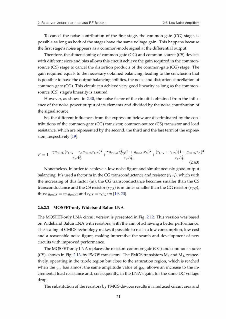
The MOSFET-only LNA circuit version is presented in Fig. 2.12. This version was basedon Wideband Balun LNA with resistors, with the aim of achieving a better performance.The scaling of CMOS technology makes it possible to reach a low consumption, low costand a reasonable noise figure, making imperative the search and development of newcircuits with improved performance.
The MOSFET-only LNA replaces the resistors common-gate (CG) and common- source(CS), shown in Fig. 2.13, by PMOS transistors. The PMOS transistors M3 and M4, respec-tively, operating in the triode region but close to the saturation region, which is reachedwhen the gm has almost the same amplitude value of gds, allows an increase to the in-cremental load resistance and, consequently, in the LNA’s gain, for the same DC voltagedrop.
The substitution of the resistors by PMOS devices results in a reduced circuit area and
21

2. RECEIVER ARCHITECTURES AND RF BLOCKS 2.7. Mixer
Vbias
Rs
M3
M1
Zin
Vout1
Vi
Ib
M2
M4
Vout2
VDD
Figure 2.13: MOSFET-only Wideband Balun LNA
cost, minimizes the effect of process variation, supply variation and mismatch. Also, op-timizes the gain of the LNA and minimize the noise figure by controlling the polarizationstate of PMOS transistors.
Regarding the original LNA, this circuit has the disadvantage of an increased distor-tion and a reduction in bandwidth.
This subsection on wideband LNA is important for the comprehension of some topolo-gies, but also to help in the understanding of Chapter 3 that focuses on the developmentof the proposed circuit [21].
2.7 Mixer
As fundamental blocks in an RF analog front-end receiver circuit, the mixers have thefunction of frequency translation of the input signal, Radio Frequency (RF) signal to abaseband or an Intermediate Frequency (IF) signal, where this process is known as down-conversion. The mixer operates as a multiplication operation which is performed by twoinputs, the Local Oscillator (LO) signal and the Radio Frequency (RF) signal, obtainingtwo signals with equal frequencies to both sum and difference of the input frequencies.
The mixers have different types of possible implementations: the active and passivemixers.
Therefore, the mixer conversion gain is important for relax the performance require-ments of both previous topologies and following blocks. The voltage conversion gain isdefined by 2.41 as the ratio of the root-mean-square (RMS) voltage of the IntermediateFrequency (IF) signal and the root-mean-square (RMS) voltage of the Radio Frequency
22

2. RECEIVER ARCHITECTURES AND RF BLOCKS 2.7. Mixer
(RF) signal:
Voltage Gain(dB) = 20log(VoutVin
)(2.41)
It can be seen as a measure of the mixing efficiency and allows distinguish the passivemixer having conversion loss (CL) from the active mixer having conversion gain (CG).
The mixing is a nonlinear operation and when nonlinear devices, such as MOS tran-sistors, are used for mixing higher operation, order effects and intermediation issuesappear. In the third-order intermodulation distortion can be generated two harmonics,which is difficult to filter without removing the IF signal. So, the levels of third-orderproducts can be verified from the Input Reference Intercept Point (IIP3), which usesthe power of the Radio Frequency (RF) input and output to increase the direct down-converted product.
This subsection will be focused on two types of mixer topologies referring the maincharacteristics and properties of each [10, 11].
2.7.1 Active Mixer
Active mixers provide gain and strength to the IF signal, as they deliver it to subsequentreceiver stages. They are most commonly based in differential pair and can be single-balanced or double-balanced, depending on whether the RF signal coming from the LNAis balanced or unbalanced.
VLO
M1 M2
VIF
VDD
M3VRF
RD RD
Figure 2.14: Single Balanced Mixer
The single-balanced active mixer, represented in Fig. 2.14, has a differential pair with
23

2. RECEIVER ARCHITECTURES AND RF BLOCKS 2.7. Mixer
the inputs driven by the LO signals, applied at the both gates, and a current source con-trolled by the RF unbalanced signal. The RF input voltage is converted to current that isdrawn alternately by the two sides of the differential pair and they preferably switchedbetween saturation region and OFF states. For this mixer, the output spectrum includesthe LO frequency. It is a simple active mixer that has moderate gain and noise figure,high input impedance and low 1 dB compression point, low IIP3 and low port-to-portisolation.
The double-balanced active mixer, represented in Fig. 2.15, called Gilbert cell, is morecomplex, having Local Oscillator (LO) and Radio Frequency (RF) differential inputs.It features improvements when compared to the single-balanced active mixer, namelyhigher gain, lower noise figure, high port-to-port isolation and good linearity. It is alsoable to remove the local oscillator (LO) frequency from the output spectrum. These im-provements increase the power consumption and circuit area and cost. A reduction ofthe supply voltage leads to worse linearity performance.
VLO
M1 M2
VIF
VDD
M3VRF
RD
M4 M5
M6
RD
Ib
Figure 2.15: Gilbert Cell
The voltage conversion gain (CG) is given by:
Av =2
πgm1RL(2.42)
There are two ways to increase the mixer gain by increasing the current flowingthrough the transconductors or increasing the load impedance or both them [10, 11, 22,23].
24
2. RECEIVER ARCHITECTURES AND RF BLOCKS 2.7. Mixer
2.7.2 Passive Mixer
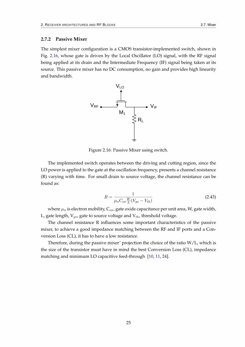
The simplest mixer configuration is a CMOS transistor-implemented switch, shown inFig. 2.16, whose gate is driven by the Local Oscillator (LO) signal, with the RF signalbeing applied at its drain and the Intermediate Frequency (IF) signal being taken at itssource. This passive mixer has no DC consumption, no gain and provides high linearityand bandwidth.
VLO
VRF
RL
M1
VIF
Figure 2.16: Passive Mixer using switch.
The implemented switch operates between the driving and cutting region, since theLO power is applied to the gate at the oscillation frequency, presents a channel resistance(R) varying with time. For small drain to source voltage, the channel resistance can befound as:
R =1
µnCoxWL (Vgs − Vth)
(2.43)
where µn is electron mobility, Cox, gate oxide capacitance per unit area, W, gate width,L, gate length, Vgs, gate to source voltage and Vth, threshold voltage.
The channel resistance R influences some important characteristics of the passivemixer, to achieve a good impedance matching between the RF and IF ports and a Con-version Loss (CL), it has to have a low resistance.
Therefore, during the passive mixer’ projection the choice of the ratio W/L, which isthe size of the transistor must have in mind the best Conversion Loss (CL), impedancematching and minimum LO capacitive feed-through [10, 11, 24].
25

2. RECEIVER ARCHITECTURES AND RF BLOCKS 2.7. Mixer
26

3Low-voltage receiver analog
front-end
A design of a low-voltage CMOS RF receiver has been proposed and the complete circuitimplementation is shown in Fig. 3.7. The building blocks of this circuit are the LNA, themixer, the LO and the TIA. The TIA is able to buffer the final output, filter frequencieshigher than the chosen IF frequency and convert the current signal to a voltage signal. ADC voltage source is added between the mixer and the TIA as a common-mode voltagefor the TIA inputs. The presented receiver circuit does not include the design of theoscillator, OTA block from the TIA.
The organization of this chapter is divided by the LNA and the receiver subsections.In both subsections some theoretical expressions and characteristics are analysed. In thereceiver front-end subsection an overall notion of the most important characteristics andparticularities of all blocks is given. In the same subsection the mixer structure is high-lighted with more detail. However, both the LNA and mixer structures were alreadyknown and didn’t constitute an actual novelty by themselves. Some novel considera-tions are taken into account, as will be shown in the following subsections. The maincontribution of the presented circuit is not the introduction of a new LNA and mixer ar-chitectures, but rather a new implementation of their combination: the signals are treatedin current mode.
27

3. LOW-VOLTAGE RECEIVER ANALOG FRONT-END 3.1. LNA
3.1 LNA
The proposed LNA circuit is presented in Fig. 3.1, it’s wideband balun LNA composedby two stages: a common-gate (CG) and common-source (CS) stage. The balun func-tionality is important for the LNA performance because in its entry has a single-ended,unbalanced input and provides a balanced output. This balanced output is a consequenceof the matching magnitudes of the two gains stages when their values are approximate.
It can be said that the proposed LNA is a new version of the MOSFET-only LNApresented in section 2.6.2.3, designed to work at VDD supply voltage of 0.6 V. The de-sign optimization and several processes have been taken into account to make the LNAworking with this VDD value without losing too much gain, such as the meticulous di-mensioning of the transistors, the use of a low-voltage technique and the introductionof independent stage biasing, that will be shown in chapter 4 with the values and thesimulations results.
The current output of the LNA can be optimised by using PMOS active devices loadsthat through the adjustments of their dimensions can increase the LNA’s output resis-tance. The PMOS devices not only help to increase the output resistance of the LNA,as well as they are responsible for the improving of the LNA’s voltage gain and noise.However, the LNA’s voltage gain is not the main concern, but rather its transcondutancegain, which is essentially given by the transistorsM1 andM2 gm values. The fact that theLNA’s output resistance depends on the dimensions of PMOS devices is relevant becausethe chosen mixer works in current mode, which will be explained in section 3.2.1.
The biasing voltage from the common-gate (CG) stage (Vbias1) applied in the transistorM1 gate terminal is limited to the supply voltage value, for that reason it wouldn’t besufficient to assure both transistors M1 and M2 gate-source voltage (Vgs) needed values.Therefore, an additional biasing voltage was added to the common-source (CS) stage theVbias2 to ensure enough gate-source voltage (Vgs) across transistor M2. Also, along withthe Vbias2 was added between the stages of the LNA the decoupling capacitor C1, to helpstop the influence among them. These changes in the LNA circuit allow the reduction ofthe VDD.
Additionally, the Dynamic Threshold MOS (DTMOS) low-voltage technique is usedin transistor M1 to allow the low supply voltage operation. The technique consists inconnecting the bulk of the transistor to its gate terminal [25, 26], introducing a dynamicregulation of the transistor’s threshold voltage. The use of this technique allows enoughdrain-source voltage (Vds) for the current-source transistor connected to the LNA’s firststage, which substitutes the ideal current source presented in Fig. 3.1. It does so by re-ducing the threshold voltage of transistor M1. The DTMOS technique is also responsiblefor a small increase in the effective gm of device M1, slightly contributing to the CG volt-age gain. The DTMOS technique also has some disadvantages, such as the increase ofthe parasitic capacitances, in this case on the transistor M1 and the possibility of latch-upappearance. The latch-up will not be an issue for this work because the whole circuit
28

3. LOW-VOLTAGE RECEIVER ANALOG FRONT-END 3.1. LNA
voltages supply is lower than 0.7 V, which is the typical problematic threshold that thelatch-up effect becomes a problem. The increase of parasitic capacitances decreases thebandwidth (BW), but they aren’t relevant to reflect a problematic situation in terms of theBW. Therefore, the choice of this low-voltage technique becomes the best choice regard-ing the other techniques for the same purpose [25, 26].
Vbias1
Rs
M3
M1
Zin
Vout1
Vin
Ib
M2
M4
Vout2
VDD
Vbias2
C1
R1
Figure 3.1: Proposed LNA Circuit.
3.1.1 Gain
The small signal model for low frequencies of the LNA proposed is represented in Fig. 3.2.Since the signal Vin is applied in the transistor M1 source terminal, the bulk effect has tobe considered. However, due to the use of the DTMOS technique on the transistor M1
where consists of connecting the bulk to the gate terminal, the body effect contributespositively to the CG voltage gain. The body effect appears due the transistor configura-tion where the source and bulk terminals don’t have the same value. So, the body effectis represented in the incremental analysis by a voltage controlled current source (VCVS)which is dependent on bulk-source voltage (Vbs).
The expression for the LNA differential voltage gain is achieved by the subtractionof the CG and CS voltage gains, which were deduced using the Fig. 3.2. To obtain thevoltage gain of the two stages, a nodal analysis is performed at nodes N1 and N2 usingthe rules of KVL (Kirchhoff’s Voltage Law) as established.
The considerations Vgs1 = −Vin and Vbs1 = −Vin are taken from the node N1:
gm1vgs1 + (vout1 − vin)gds1 + gmb1vbs1 + vout1gds3 + gm3vgs3 = 0 (3.1)
29

3. LOW-VOLTAGE RECEIVER ANALOG FRONT-END 3.1. LNA
G1
ii
Vin
vgs1vbs1
gm1.vgs1
gmb1.vbs1
rds1 rds3 gm3.vgs3
S3
G3D3
S1
B1
D1 G2
S2
R1
D2 D4 G4
S4
gm2.vgs2 gm4.vgs4
rds2 rds4
Vout2Vout1
Figure 3.2: The small signal model for low frequencies of the LNA.
At node N2 is taken into account the consideration Vgs2 = Vin:
gm2vin + vout2(gds2 + gds4) + gm4vgs4 = 0 (3.2)
With the respective substitutions from 3.1 the common-gate (CG) gain is,
AvCG =Vout1Vin
=gm1 + gmb1 + gds1
gds1 + gds3(3.3)
Can be expressed also:
AvCG =((gm1 + gmb1)rds1) + 1)rds3
rds1 + rds3(3.4)
In the case where it’s considered that the resistance RS and the signal Vin are appliedtogether on the source terminal of the transistor M1. The current in2 is taken at node N2and some considerations are i = Vout1/rds3 and Vgs1 = i.Rs − Vin:
in2 =Vout1rds3
+ (gm1 + gmb1)Vgs1 (3.5)
From the KVL rule, Vout1 can be expressed as:
Vout1 = Vin − i.Rs − in2rds1 (3.6)
The voltage gain of CG stage is:
AvCG[Rs] =Vout1Vin
=rds3(1 + rds1(gm1 + gmb1))
rds3 + rds1 +Rs(1 + rds1(gm1 + gmb1))(3.7)
The result of common-source(CS) gain ( 3.8) is obtained by the same procedure of thecommon-gate (CG) gain ( 3.3), but in this case is made the manipulation of the expression3.2.
AvCS =Vout2Vin
= − gm2
gds2 + gds4(3.8)
30

3. LOW-VOLTAGE RECEIVER ANALOG FRONT-END 3.1. LNA
The common-source (CS) stage gain can also be expressed through output resistances:
AvCS = −gm2(rds2‖rds4) = −gm2rds2rds4rds2 + rds4
(3.9)
The LNA differential voltage gain is obtained through the subtraction of ( 3.3) and( 3.8):
Avdiff =Vout1 − Vout2
Vin=gm1 + gmb1 + gds1 + gm2(
gds1+gds3gds2+gds4
)
gds1 + gds3(3.10)
The approximate expression for the LNA differential voltage gain is possible to getit if it’s considered that the values of gds1 and gds2 (gds1≈gds2) and the values of gds3 andgds4 (gds3≈gds4) are similar between them.
Avdiff ≈gm1 + gmb1 + gm2
gds1 + gds3(3.11)
3.1.2 LNA input-impedance
The LNA input-impedance expression (Zin) is achieved from the transistor M1 sourceterminal, as shown in Fig. 3.1. It’s obtained through the analysis of the small signal forlow frequency as shown in Fig. 3.2, where is verified the current ii flowing through thetransistor source.
−ii− gm1vgs1 − gmb1vbs1 − (vout1 − vin)gds1 = 0 (3.12)
The considerations Vgs1 = Vbs1 = −Vin are substituted in the expression 3.12 to obtaina simpler current expression 3.13.
ii = gm1vin + gmb1Vin − Vout1gds1 + Vingds1 (3.13)
1
Zin=
ii
Vin(3.14)
Noting that 3.14 and then substituting on it with the current expression 3.13, thefollowing expression is obtained:
1
Zin=Vin(gm1 + gmb1 + gds1)− Vout1gds1
vin(3.15)
Using the expression of the common-gate (CG) gain ( 3.3) to replace Vout1 in the ex-pression 3.15, we obtain the input-impedance:
Zin =gds1 + gds3
(gm1 + gmb1 + gds1)gds3(3.16)
31

3. LOW-VOLTAGE RECEIVER ANALOG FRONT-END 3.1. LNA
3.1.3 Noise Factor
The complete LNA’s noise factor is formed by three main noises sources: the thermalnoise influenced by the transistors and resistors and the flicker noise generated by tran-sistors. The LNA circuit, shown in Fig. 3.1, had to suffer some approaches and consider-ations, in order to simplify the analysis of the noise factor, demonstrated in the Fig. 3.3.These are the following ones:
Vbias1
Rs
M1
Vout1
Ib
M2
Vout2
VDD
Rds3
Vs
Rds4
In,1
VinVn,in
Vn,out2Vn,out1
In,2
In,M4In,M3
Figure 3.3: The result of the LNA circuit’ approaches and approximations, includingsome noise sources.
• The thermal noise’s effect that is generated by the source resistor RS and the inputsource of CG stage is neglected at the beginning of this analysis, but afterwards isconsidered in the final equation, as will be established ( 3.48).
• The thermal noise generated by the transistor M1 of the CG stage is representedby the current source (in,1) which corresponds the current that flows into to re-sistor RS , producing a noise voltage (Vn,in) at the input of CG stage. The noisevoltage (Vn,in) is opposed to the output noise of the CG stage (Vn,out1) and in phasewith the output noise CS stage (Vn,out2), their respective associated conditions are:Vn,out1 = −Vn,inAvCG and Vn,out2 = Vn,inAvCS . The thermal noise produced bytransistor M1 is cancelled if the Balun conditions are satisfied. Which means thatthe CG and CS gains should be equals (AvCG = −AvCS) to obtain a balanced differ-ential output and cancellation of thermal noise of the M1.
• The PMOS transistors (M3 andM4) were dimensioned as LNA’s output resistances,
32

3. LOW-VOLTAGE RECEIVER ANALOG FRONT-END 3.1. LNA
its area of operation is the triode zone which considered that gm << gds. Therefore,for the analysis of the LNA’s noise factor was neglected the gm effect on theM3 andM4 transistors and considered as typically resistances rds3 and rds4 (dimensions inthe order of ohms), respectively, demonstrated in the Fig. 3.3.
• The thermal noise effect of the resistor R1 is negligible in the overall noise factor ofthe LNA. Although the resistor R1’ dimension has an order of Kohms compared tothe dimensions of the LNA’s output resistances (rds3 and rds4), the current sourcethat is applied in parallel with R1 to obtain the thermal noise is In,R1 = 4kT/R1. Sotheir contribution isn’t relevant to the total noise factor.
• The effects of the parasitic capacitances are negligible because the LNA’s noise fac-tor is at low frequencies.
Initially, this analysis will be done by separating the LNA stages and considers eachnoise source at once.
Common-gate (CG) stage
The Fig. 3.4 represents all noise sources in the common-gate (CG) circuit and smallsignal model. From the superposition theorem and assuming that the noise sources aren’tcorrelated, each noise source is analysed independently.
Flicker noise: The flicker noise source in the gate of transistor M1 (Vn,f ) is modeled inseries with a voltage (Vnf1,out), shown in Fig. 3.4(b), with the conditions mentioned above.
Considering the voltage that goes to the gate until ground Vn,f = Vgs1 − Vbs1 , theexpression ( 3.17) of bulk-source voltage is:
Vbs1 = iiRs (3.17)
Substituting the expression ( 3.17) on (Vn,f = Vgs1 − Vbs1):
Vgs1 = iiRs + Vn,f (3.18)
At node 1 is taken the current (ii):
ii = −(gm1Vgs1 + gmb1Vbs1) +(−Vbs1 − Vnf1,out)
rds1(3.19)
33

3. LOW-VOLTAGE RECEIVER ANALOG FRONT-END 3.1. LNA
Vn,f2
Rs
Rds3
M1
Vn1,out2
Vn,RS2
VDD
In,M32
In,12
(a) CG circuit
G1
ii
vgs1
gm1.vgs1
gmb1.vbs1
rds1 rds3
D1
Rs
Vn,RS2
Vn,f2
S1
In,M32
Vn1,out2
In,12
(b) The small signal model for low frequencies of CG circuit
Figure 3.4: Common-gate (CG) model for all the noise contributions.
34

3. LOW-VOLTAGE RECEIVER ANALOG FRONT-END 3.1. LNA
Using the equations ( 3.17) and ( 3.18), then substituting on ( 3.19) and solving in orderii:
ii =−gm1Vn,f − gds1Vnf1,out
1 +Rs(gm1 + gmb1 + gds1)(3.20)
The output noise voltage (Vnf1,out) from the flicker noise (Vn,f ) is calculated by sub-stituting the equation ( 3.20) on ( 3.21) and solving in order Vnf1,out:
Vnf1,out = iirds3 = − gm1rds1rds3rds1 +Rs(rds1(gmb1 + gm1) + 1) + rds3
Vn,f (3.21)
The output voltage noise power (Vnf1,out2) is:
V 2nf1,out =
(gm1rds1rds3
rds1 +Rs(rds1(gmb1 + gm1) + 1) + rds3
)2
Vn,f2
=
(gm1rds1rds3
rds1 +Rs(rds1(gmb1 + gm1) + 1) + rds3
)2kf
coxW1L1fαf
(3.22)
Thermal noise: The thermal noise source in transistorM1 is presented as a current source(In,1) between the drain and the source, shown in Fig. 3.4(b).
From the condition (Vgs1 = Vbs1) the gate-source voltage is,
Vgs1 = iiRs (3.23)
The current that flows in the resistance rds3 is:
ii = −(gm1 + gmb1)Vbs1 + In,1 +
(−Vbs1 − Vn1,out
rds1
)(3.24)
By substituting ( 3.23) on ( 3.24), the expression ( 3.25) is solved on ii:
ii =In,1 − gds1Vn1,out
1 +Rs(gm1 + gmb1 + gds1)(3.25)
The output thermal noise (Vn1,out) is calculated from the thermal noise source (In,1)when ( 3.25) is substituted on ( 3.26):
Vn1,out = iirds3 =In,1rds1rds3
rds1 +Rs(rds1(gm1 + gmb1) + 1) + rds3(3.26)
35

3. LOW-VOLTAGE RECEIVER ANALOG FRONT-END 3.1. LNA
The thermal noise power at the output (Vn1,out2) is:
Vn1,out2 = In,1
2
(rds1rds3
rds1 +Rs(rds1(gm1 + gmb1) + 1) + rds3
)2
= 4KTγgm1
( rds1rds3rds1 +Rs(rds1(gm1 + gmb1) + 1) + rds3
)2(3.27)
Thermal noise due to the resistance rds3: The thermal noise source (In,M3) of the resis-tance rds3 is modeled as a current source parallel to it, as shown in Fig. 3.4.
To obtain the expression of the output noise (VnM3,out) from the thermal noise source(In,M3), the RS is neglected (RS = 0), so the small signal incremental model is simplified(Fig. 3.5).
rds1 rds3In,M32
VnM3,out2
Figure 3.5: The approximate small signal model of CG circuit.
VnM3,out = In,M3(rds1‖rds3) (3.28)
Considering the condition Vgs2 = 0 and ( 3.28), the thermal noise power of the output(VnM3,out) is:
VnM3,out2 = In,M3
2(rds1‖rds3)2 =4KT
rds3(rds1‖rds3)2 (3.29)
In the case of considering the resistance Rs, the output thermal noise (VnM3,out) iscalculated by rely on the input noise (Vn,in) and on the CG gain stage ( 3.4):
VnM3,out2 = Vn,in
2AvCG2 (3.30)
By substituting ( 3.28) and the gain ( 3.4) on the expression ( 3.31), the input noisepower (Vn,in2) is,
Vn,in2 =
4KTrds3(rds1)2
((rds1(gm1 + gds1) + 1)rds3)2 (3.31)
The output noise power (VnM3,out2) of the circuit ( 3.3) is calculated by multiplying
the input noise power ( 3.31) and the transfer function obtained in ( 3.7) that corresponds
36

3. LOW-VOLTAGE RECEIVER ANALOG FRONT-END 3.1. LNA
to the CG gain expression that includes the resistance Rs. The noise power at the outputis,
VnM3,out2 =
4KTrds3(rds1)2
((rds1(gm1 + gds1) + 1)rds3Rs + rds1 + rds3)2 (3.32)
Common-source (CS) stage
All noise sources of the common-source (CS) circuit and the incremental analysismodel are represented in Fig. 3.6. Assuming that the analysis of each noise source isindependent and uncorrelated, that’s why it’s used the superposition theorem.
Vn,f2
Rs
Rds4
M2
Vn2,out2
Vn,RS2
VDD
In,M42
In,22
(a) CS circuit
iiG2
S2
D2
gm2.vgs2
rds2 rds4
Rs
Vn,RS2
Vn,f2
In,M42
In,22
Vn2,out2
vgs2
(b) The small signal model for low frequencies of CS circuit
Figure 3.6: Common-source (CS) model for all the noise contributions.
Flicker Noise: The flicker noise source (Vn,f ) of the transistor M2 is modeled as a voltagesource in series with the gate, shown in Fig. 3.6(b).
37

3. LOW-VOLTAGE RECEIVER ANALOG FRONT-END 3.1. LNA
The flicker noise power at the output (Vnf2,out2) is calculated using the transfer func-tion of the CS gain ( 3.8):
Vnf2,out2 = Vn,f
2AvCS2 =
kfW2L2coxfαf
gm22
(rds2rds4rds2 + rds4
)2
(3.33)
Thermal Noise: The current source (In,2) lying between the drain and the source of tran-sistor M2 is used as the presentation of the thermal noise source.
As shown in Fig. 3.6(b), the current source In,2 is,
In,22 = 4KTgm2 (3.34)
The output noise power (Vn2,out2) due to the current source In,2 is,
Vnf2,out2 = In,2
2(rrds2‖rds4)2 = 4KTgm2
(rds2rds4rds2 + rds4
)2
(3.35)
Thermal noise due to the resistance rds4: It’s represented as a current source (In,M4)parallel to resistance rds4.
In,M42 =
4KT
rds4(3.36)
Taking into account that Vgs2 = 0, the output noise power (VnM4,out2) is:
VnM4,out2 = In,M4
2(rrds2‖rds4)2 =4KT
rds4
(rds2rds4rds2 + rds4
)2
(3.37)
After acquiring the individual analysis of each noise stage, it’s necessary obtained thenoise contributions that are from the CG stage and will appear at the CS output stageand vice-versa. To access this effect, the input referred represents the noise generatedby the stage that will influence the other, divided by its own gain and then amplified bythe influenced stage. Furthermore, to simplified the complete noise power process, thenoise effect that is generated by the source resistor RS and the input source of CG stageis neglected, but added in final equation ( 3.48).
38
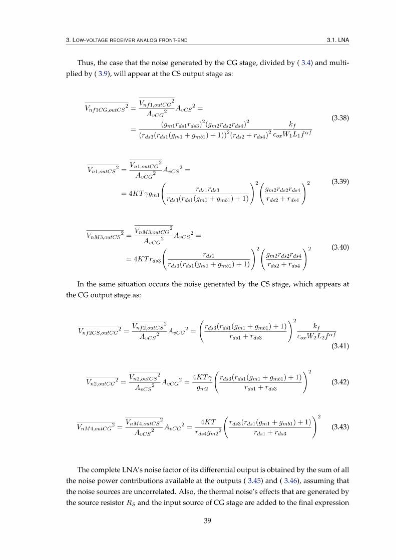
3. LOW-VOLTAGE RECEIVER ANALOG FRONT-END 3.1. LNA
Thus, the case that the noise generated by the CG stage, divided by ( 3.4) and multi-plied by ( 3.9), will appear at the CS output stage as:
Vnf1CG,outCS2 =
Vnf1,outCG2
AvCG2 AvCS
2 =
=(gm1rds1rds3)
2(gm2rds2rds4)2
(rds3(rds1(gm1 + gmb1) + 1))2(rds2 + rds4)2
kfcoxW1L1fαf
(3.38)
Vn1,outCS2 =
Vn1,outCG2
AvCG2 AvCS
2 =
= 4KTγgm1
(rds1rds3
rds3(rds1(gm1 + gmb1) + 1)
)2(gm2rds2rds4rds2 + rds4
)2 (3.39)
VnM3,outCS2 =
VnM3,outCG2
AvCG2 AvCS
2 =
= 4KTrds3
(rds1
rds3(rds1(gm1 + gmb1) + 1)
)2(gm2rds2rds4rds2 + rds4
)2 (3.40)
In the same situation occurs the noise generated by the CS stage, which appears atthe CG output stage as:
Vnf2CS,outCG2 =
Vnf2,outCS2
AvCS2 AvCG
2 =
(rds3(rds1(gm1 + gmb1) + 1)
rds1 + rds3
)2kf
coxW2L2fαf
(3.41)
Vn2,outCG2 =
Vn2,outCS2
AvCS2 AvCG
2 =4KTγ
gm2
(rds3(rds1(gm1 + gmb1) + 1)
rds1 + rds3
)2
(3.42)
VnM4,outCG2 =
VnM4,outCS2
AvCS2 AvCG
2 =4KT
rds4gm22
(rds3(rds1(gm1 + gmb1) + 1)
rds1 + rds3
)2
(3.43)
The complete LNA’s noise factor of its differential output is obtained by the sum of allthe noise power contributions available at the outputs ( 3.45) and ( 3.46), assuming thatthe noise sources are uncorrelated. Also, the thermal noise’s effects that are generated bythe source resistor RS and the input source of CG stage are added to the final expression
39
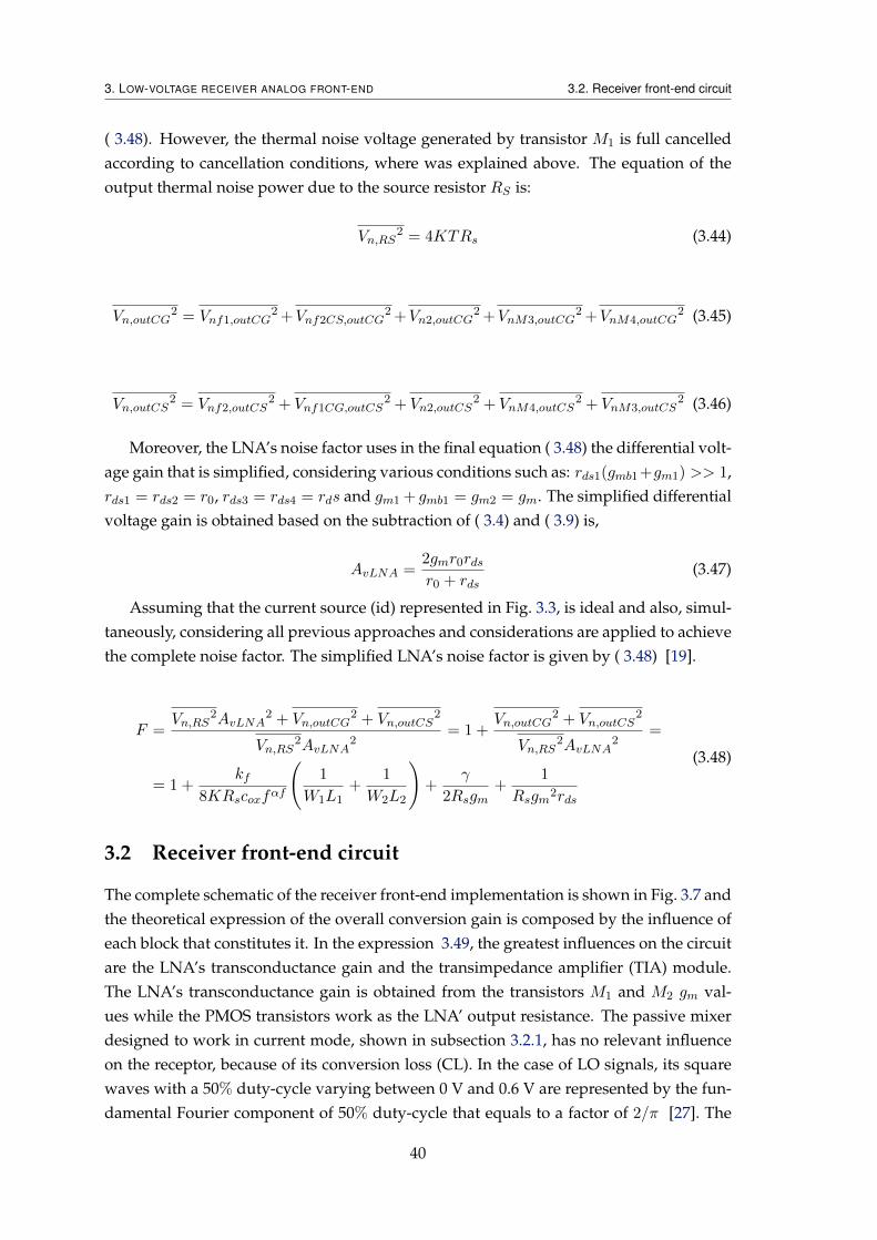
3. LOW-VOLTAGE RECEIVER ANALOG FRONT-END 3.2. Receiver front-end circuit
( 3.48). However, the thermal noise voltage generated by transistor M1 is full cancelledaccording to cancellation conditions, where was explained above. The equation of theoutput thermal noise power due to the source resistor RS is:
Vn,RS2 = 4KTRs (3.44)
Vn,outCG2 = Vnf1,outCG
2 +Vnf2CS,outCG2 +Vn2,outCG
2 +VnM3,outCG2 +VnM4,outCG
2 (3.45)
Vn,outCS2 = Vnf2,outCS
2 + Vnf1CG,outCS2 + Vn2,outCS
2 + VnM4,outCS2 + VnM3,outCS
2 (3.46)
Moreover, the LNA’s noise factor uses in the final equation ( 3.48) the differential volt-age gain that is simplified, considering various conditions such as: rds1(gmb1+gm1) >> 1,rds1 = rds2 = r0, rds3 = rds4 = rds and gm1 + gmb1 = gm2 = gm. The simplified differentialvoltage gain is obtained based on the subtraction of ( 3.4) and ( 3.9) is,
AvLNA =2gmr0rdsr0 + rds
(3.47)
Assuming that the current source (id) represented in Fig. 3.3, is ideal and also, simul-taneously, considering all previous approaches and considerations are applied to achievethe complete noise factor. The simplified LNA’s noise factor is given by ( 3.48) [19].
F =Vn,RS
2AvLNA2 + Vn,outCG
2 + Vn,outCS2
Vn,RS2AvLNA
2= 1 +
Vn,outCG2 + Vn,outCS
2
Vn,RS2AvLNA
2=
= 1 +kf
8KRscoxfαf
(1
W1L1+
1
W2L2
)+
γ
2Rsgm+
1
Rsgm2rds
(3.48)
3.2 Receiver front-end circuit
The complete schematic of the receiver front-end implementation is shown in Fig. 3.7 andthe theoretical expression of the overall conversion gain is composed by the influence ofeach block that constitutes it. In the expression 3.49, the greatest influences on the circuitare the LNA’s transconductance gain and the transimpedance amplifier (TIA) module.The LNA’s transconductance gain is obtained from the transistors M1 and M2 gm val-ues while the PMOS transistors work as the LNA’ output resistance. The passive mixerdesigned to work in current mode, shown in subsection 3.2.1, has no relevant influenceon the receptor, because of its conversion loss (CL). In the case of LO signals, its squarewaves with a 50% duty-cycle varying between 0 V and 0.6 V are represented by the fun-damental Fourier component of 50% duty-cycle that equals to a factor of 2/π [27]. The
40

3. LOW-VOLTAGE RECEIVER ANALOG FRONT-END 3.2. Receiver front-end circuit
VLO+
M5 M7M6VLO-M8
Vbias1
Rs
M3
M1
Vout1
Vin
Ib
M2
M4
Vout2
VDD
Vbias2
C1
R1
C2
C3
R3
R2
R5
R4
C4
C5
VCM
Figure 3.7: Complete Receiver Circuit.
TIA filter, in this case a Low-Pass Filter (LPF), is made by passive components, a combina-tion of resistor and capacitor, that defines a conveniently dimensioned cut-off frequency,fc. This fc frequency was set at a value that is slightly higher than the IF frequency, sothat higher frequencies are cut-off. The voltage conversion gain from single-ended inputto differential output of the receiver topology is given by ( 3.49).
V GTotal =2
πgmLNAZTIAFilter@10MHz (3.49)
The RF signal coming from the antenna is amplified and converted to a current signalby the LNA, being delivered to the mixer as a balanced signal. The mixer’s output, abalanced current signal, IF, is then converted to a balanced voltage signal by the TIA. Asit’s shown in equation ( 3.49), the LNA’s transconductance gain is given by the gm values,because of the conversion of the RF voltage signal to a current signal. Also, the TIAmodule contributes to equation ( 3.49) with its impedance value, since the TIA moduleconverts the current signal coming from the mixer to a voltage signal at the proposedreceiver’s output.
3.2.1 Mixer
The mixer architecture chosen to be integrated in the receiver is a passive mixer. Thecircuit is presented in Fig. 3.8 and is constituted by two pairs of NMOS used as voltage-controlled switches. The gates of the switches that constitute the mixer are driven by theLocal Oscillator (LO) signals, with the Radio Frequency (RF) signals being applied at itssource and the Intermediate Frequency (IF) signals being taken at its drain.
The main purpose of this architecture choice is the power consumption, which is amajor requirement for the overall operation of the WSAN receiver. The two pairs ofNMOS transistors are working in the triode zone to maintain a low drain-source voltagewhen they are switched ON. These NMOS transistors are cut-off when switched OFF.The mixer works as a current commutating mixer which means that the RF signals at themixer’ input are mixed in current. The LO signals that drive the devices’ gates must be
41

3. LOW-VOLTAGE RECEIVER ANALOG FRONT-END 3.2. Receiver front-end circuit
VLO+M5 M7M6
VRF
VLO-M8
VIF
Figure 3.8: Mixer architecture.
strong and buffered; they vary from 0 V to 0.6 V, the VDD supply voltage. The IF outputsignal is a balanced signal, due to the mixer’s structure.
The factors that allow the mixer to work in current mode are the inclusion of theDC decoupling capacitors, the LO signals that drive the devices’ gates and the common-mode voltage source at the TIA’s input. The current mode minimizes the introductionof noise and ensures a good linearity. The reduced noise introduction, especially flickernoise, is possible due to the inclusion of the DC decoupling capacitors between the LNAand mixer, which guarantee there is no DC current flowing through the mixer. Moreover,due to the TIA, the variation of the drain-source voltage of the mixer’s NMOS is reduced,thus contributing to improve the linearity of the circuit. The circuit’ gain can be definedby the quotient between the IF signal amplitude and the RF signal amplitude. The passivemixer has a conversion gain that is less than one, so it presents a small Conversion Loss(CL).
42

4Receiver Implementation
The detailed analysis of the theoretical expressions and characteristics present in the pre-vious chapter are used to implement a low-voltage RF receiver in 130 nm CMOS technol-ogy presents the dimensioning of the proposed receiver circuit, as well as the schematicand post-layout simulations.
The section 4.1 introduces the considerations, simulations and validation of the im-plemented receiver, as well as the first block, the LNA, because of its importance andinfluence on the final results of the entire circuit. While in the post-layout section ispresented the final design, the simulation results, the comparison between the obtainedvalues before and after the layout and the problems that emerged. Finally, a brief discus-sion of the results is made and is verified if the circuit satisfies the requirements for thetarget application.
4.1 Considerations, simulations and validation of the proposedcircuit
The dimension process for a low-voltage CMOS RF receiver has to be guided by theobjectives that affect the target application for which the whole circuit was intended.The process was initiated when the classic schematics for each block of the receiver werechosen, with the simplicity and possibility criteria of working together to achieve thepurpose of the target application. With all that being said the low-power consumptionand low-voltage supply operations are the main scoops of this project.
The consideration process began by defining the VDD voltage and power consump-tion values, which in this case, the VDD voltage was set at 0.6 V. The restructuring and
43

4. RECEIVER IMPLEMENTATION 4.1. Considerations, simulations and validation of the proposed circuit
modification began on the first block, the LNA, where the ideal current source was sub-stituted by a current mirror, shown in Fig. 4.1 , biasing the first stage of the LNA with acurrent value of approximately 1.64 mA, the Vbias1 was set at 0.6 V and Vbias2 at 0.45 V.
The initial dimensions of the transistors which are shown in Table 4.1, had to take intoaccount several factors. In the case of LNA, using equation ( 3.16), the dimensions of thetransistor M1 were manipulated to ensure the 50 Ω input matching, from the definitionof its width (WM1). The two stages presented in equations ( 3.3) and ( 3.8) have to coin-cide in value, that’s why the width WM2 value of the transistor M2 is chosen taking intoaccount the matching gains of the CG and CS stages, which is required to achieve thenoise cancelling capability, as explained the condition in section 3.1.3. Both transistorsM1 and M2 have to be in the saturation region and Vbias2 voltage is used to adjust the DCcurrent of M2 to a value close to the value of the M1. WM3 and WM4 were determined byLNA’ output impedance, which means that these values were chosen in order to definethe PMOS drain-source resistance at a desired value, initially 200 Ω.
The NMOS and PMOS transistors are chosen as RF transistors, with a triple wellstructure chosen for the NMOS. The chosen length (L) for all transistors was the min-imum value of the technology, in this case 120 nm, so that maximize the speed of thecircuit.
The chosen width values for the mixer devices were created with the objective ofachieving low values of drain-source resistance. Moreover, it’s an inductorless circuit,which helps in the reduction of the overall circuit area and, for that reason, circuit cost.
Table 4.1: Initial Dimensions of the Transistors.ID(mA) W(µm) L(µm) rds(Ω) gds(mS) gm(mS)
M1 1.64 66 0.12 453 2.2 20.15LNA M2 1.63 75.6 0.12 576 1.73 21.88
M3 1.64 52.8 0.12 254 3.93 8.6M4 1.63 53.28 0.12 257 3.89 8.5
Mixer M5,6,7,8 - 115.2 0.12 - - -
This receiver circuit doesn’t include the oscillator and the OTA designs, consider-ing them as ideal devices. However, the circuit was dimensioned to work with a RFfrequency of 1 GHz and an IF frequency of 10 MHz, thus the LO frequency was consid-ered 990 MHz. The signals that come from LO+ and LO- in Fig. 3.7 are square waves inquadrature with 50 ps of rise and fall times and without overlapping, with peak-to-peakbuffered voltages of 0.6 V.
Other important components that are responsible for the circuit behaviour are theresistors and capacitors. The values chosen for both type of components are presented intable 4.2. The resistor R1 and capacitor C1 are responsible for the independently biasingof the CS stage, as mentioned earlier in this section. While the resistors R2 and R3 helpdefine the common mode voltage at the TIA input, which is set at 100 mV by the idealvoltage VCM . The capacitor C1 is also responsible for DC decoupling between the two
44

4. RECEIVER IMPLEMENTATION 4.1. Considerations, simulations and validation of the proposed circuit
LNA stages, when the capacitors C2 and C3 allow the DC decoupling between the LNAand mixer, while achieving low impedance values at the RF frequency of interest.
On TIA, the Low-Pass Filter (LPF) is implemented by choosing the values of resistorsR4 andR5 and capacitors C4 and C5. Its cut-off frequency was dimensioned to be slightlyhigher than the IF frequency, in order to attenuate the frequencies above IF.
The TIA’s transresistance gain value, responsible for the current to voltage conver-sion, is 200 KΩ for the IF frequency (10 MHz). This value corresponds to the impedanceof the parallel of resistor R5 and capacitor C4 (or R4 and C5) for the given IF frequency,which, for simplicity, can be considered as the correspondent resistor value.
Table 4.2: Resistor and Capacitor dimensions.
R1,R2,R3(kΩ) R4,R5(kΩ) C1,C2,C3(ρF) C4,C5(ρF)
Values 10 200 5 9
Ib
(a) Current source.
NM0NM1
IbIref = 1.75 mA
(13203/0.48) (13203/0.48)
1:1
m=1 m=1
(b) Current mirror with all the transistors sizes (W/L) in µm.
Figure 4.1: The LNA’s current mirror structure.
4.1.1 LNA simulation results
Inductorless, wideband, balun, lower-power and low-voltage are some of the LNA char-acteristics of this project. In section 4.1 a detailed explanation of the chosen considera-tions and values is done. Also, the dimensions of the transistors, shown in table 4.1, arechosen, in a way that are critical for obtaining the performance parameters. This LNAwith differential output have to have a high gain and noise cancellation which causes aimprovement in the linearity.
The differential gain simulation, represented in Fig. 4.2, was performed on AC tracesimulations using the equation 3.11 as its auxiliary. The simulation result leads to theconclusion that the voltage gain circuit is approximately constant 17.9 dB up to 1 GHzand after less 3 dB its bandwidth has the value of 4.3 GHz.
45
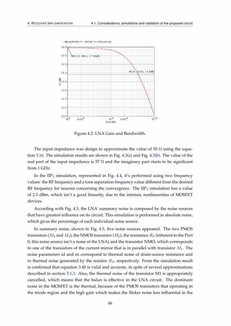
4. RECEIVER IMPLEMENTATION 4.1. Considerations, simulations and validation of the proposed circuit
Figure 4.2: LNA Gain and Bandwidth.
The input impedance was design to approximate the value of 50 Ω using the equa-tion 3.16. The simulation results are shown in Fig. 4.3(a) and Fig. 4.3(b). The value of thereal part of the input impedance is 57 Ω and the imaginary part starts to be significantfrom 1 GHz.
In the IIP3 simulation, represented in Fig. 4.4, it’s performed using two frequencyvalues: the RF frequency and a tone separation frequency value different from the desiredRF frequency for reasons concerning the convergence. The IIP3 simulation has a valueof 2.3 dBm, which isn’t a good linearity, due to the intrinsic nonlinearities of MOSFETdevices.
According with Fig. 4.5, the LNA’ summary noise is composed by the noise sourcesthat have greatest influence on its circuit. This simulation is performed in absolute noise,which gives the percentage of each individual noise source.
In summary noise, shown in Fig. 4.5, five noise sources appeared. The two PMOStransistors (M3 andM4), the NMOS transistor (M2), the resistanceRS (inherent to the Port0, this noise source isn’t a noise of the LNA) and the transistor NMO, which correspondsto one of the transistors of the current mirror that is in parallel with transistor M1. Thenoise parameters id and rn correspond to thermal noise of drain-source resistance andto thermal noise generated by the resistor RS , respectively. From the simulation resultis confirmed that equation 3.48 is valid and accurate, in spite of several approximationsdescribed in section 3.1.3. Also, the thermal noise of the transistor M1 is appropriatelycancelled, which means that the balun is effective in the LNA circuit. The dominantnoise in the MOSFET is the thermal, because of the PMOS transistors that operating inthe triode region and the high gain which makes the flicker noise less influential in the
46

4. RECEIVER IMPLEMENTATION 4.1. Considerations, simulations and validation of the proposed circuit
(a) Real Part
(b) Imaginary Part
Figure 4.3: LNA input impedance.
47
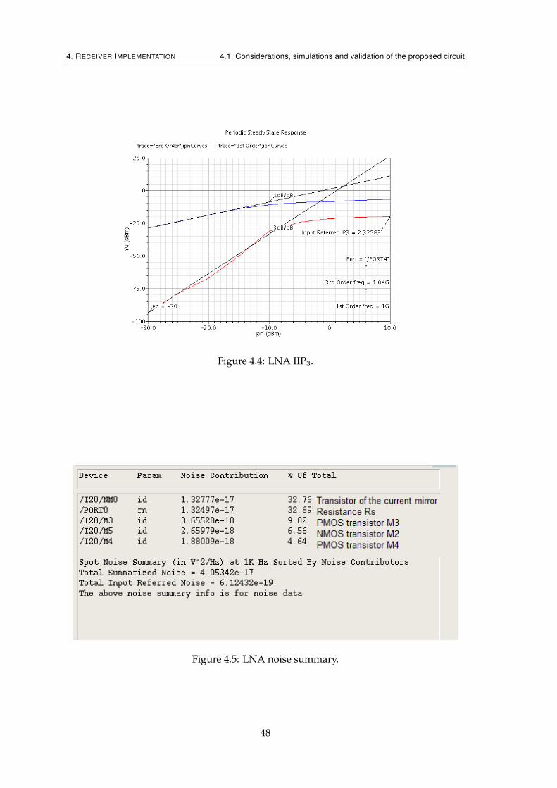
4. RECEIVER IMPLEMENTATION 4.1. Considerations, simulations and validation of the proposed circuit
Figure 4.4: LNA IIP3.
Figure 4.5: LNA noise summary.
48

4. RECEIVER IMPLEMENTATION 4.1. Considerations, simulations and validation of the proposed circuit
circuit. However, the most influential noise source of the LNA is the transistor MNOwho is part of the current mirror, as shown in the simulation result of summary noise.The current mirror isn’t considered ideal in the schematic, although it’s neglected in thefinal equation of the noise factor ( 3.48).
The noise factor simulation, shown in Fig. 4.6, was performed to validate the lownoise of the LNA. The simulation results lead to the conclusion that its value is around4.8 dB, for the value of the RF frequency.
Figure 4.6: LNA Noise Figure.
Table 4.3 shows the summary results of theoretical and schematic. The theoreticalresults are obtained using the theoretical equations, demonstrated in the chapter 3.
Table 4.3: The theoretical and schematic results of the LNA.Zin Band Gain NF Power VDD
(Ω) (GHz) (dB) (dB) (mW) supply(V)
Theoretical 59 0.1-4.9 18.3 <3.5 1.9 0.6Schematic 57 0.1-4.3 17.9 <5.2 1.9 0.6
Following the obtained results in the previous simulations, the LNA was chosen forcomparison with others state-of-the-art, inductorless and balun LNAs. The LNA is thekey block in terms of gain and distortion for the receiver circuit. The comparison of state-of-the-art LNAs is shown in Table 4.4.
The equations of consumption and FOM are presented in ( 4.1) and ( 4.2) with thepurpose to help in the comparison of the LNAs.
PDC [mW ] = VDD(ICG + ICS) (4.1)
49

4. RECEIVER IMPLEMENTATION 4.1. Considerations, simulations and validation of the proposed circuit
FoM [mW−1] =Avdiff
(NF − 1)PDC [mW ](4.2)
Table 4.4: Comparison with State-of-the-art LNAS.
Ref. Tech VDD Band Gain NF IIP3 Power FoM(nm) (V) (GHz) (dB) (dB) (dBm) (mW) (mW−1)
[19] 65 1.2 0.2 - 5.2 15.6 <3.5 >0 14 0.34[28] 90 2.5 0.8 - 6 20 <3.5 >-3.5 12.5 0.6[29] 90 1.2 0.1 - 1.9 20.6 <2.7 10.8 9.6 1.3[18] 130 1.2 0.2 - 3.8 11.2 <2.8 -2.7 1.9 2.1[21] 130 1.2 0.2 - 6.6 19.8 <1.8 1.6 4.8 3.9
This Work 130 0.6 0.1 - 4.3 17.9 <5.2 2.3 1.95 1.9
Conclusions: The LNA’s bandwidth satisfies the requirements for the target application.The LNA’s voltage gain value is equivalent to the voltage gain values of the originalMOSFET-only LNA [21] that was considered (in section 2.6.2.3), which is a positive re-sult, having in mind the VDD voltage supply reduction for the proposed circuit, in rela-tion to the original one. The power consumption has a satisfactory value compared tothe other from the table 4.4. Although the FoM result is slightly low than the other FoMLNAs, which is a drawback.
4.1.2 Receiver simulation results
The blocks that composed the receiver circuit are the LNA, mixer, LO and TIA, despite thelast two being ideal, the analysis of the performance parameters is made. In the previoussubsection, the LNA block is analysed because of its importance and influencing in therest of the circuit, in terms of gain, linearity and bandwidth. However, when all blocks aregrouped some transistors dimensions have had to be adjusted and optimized, as shownin table 4.5.
Table 4.5: Optimized transistors dimensions.
ID(mA) W(µm) L(µm) rds(Ω) gds(mS) gm(mS)
M1 1.63 66 0.12 454 2.2 20.15LNA M2 1.55 71.4 0.12 612 1.63 20.79
M3 1.63 52.8 0.12 254 3.93 8.61M4 1.55 51.2 0.12 246 4.06 8.03
Mixer M5,6,7,8 - 115.2 0.12 - - -
As explained in section 3.1 of chapter 3, the LNA has to be carefully designed with thesame magnitude value on both stages, to allow its output to be balanced and noise can-celled by satisfying the conditions balun. However, the following block after the LNA,
50

4. RECEIVER IMPLEMENTATION 4.1. Considerations, simulations and validation of the proposed circuit
the mixer, is in current mode, which means that the RF signal at the input mixer mustbe in current. The LNA’s transcondutance gain becomes essential, instead of the voltagegain, allowing the mixer to work in current mode. So, the transistors dimensions of theLNA are responsible for the RF signals, which have to have an approximate output cur-rent magnitude, as shown in Fig. 4.7. Also, in the Fig. 4.7 is possible to see the modulationeffect of the Local Oscillator (LO) leakage, which proves the need for LO signal drivers.
Figure 4.7: LNA output current.
Figure 4.8: Receiver’s noise figure.
Consequence of this changes make the magnitude of LNA’s stages slightly different,so the noise cancellation isn’t 100% and therefore, there is an attenuation on the voltage
51

4. RECEIVER IMPLEMENTATION 4.1. Considerations, simulations and validation of the proposed circuit
gain, which means that there is a slight increase in the noise factor of the LNA and con-sequently in the receiver circuit. However, the fact that the mixer works in current modeminimizes the introduction of noise, especially noise flicker, and ensures a good linearity.Moreover, there is a threshold between the LNA and the mixer in terms of noise introduc-tion in the receiver. In order to validate the low noise capabilities of the complete circuit,a noise figure simulation, shown in Fig. 4.8, was carried out for the differential IF output.The simulation’s results lead to the conclusion that the circuit presents a low noise figure,around 8.7 dB, for a relatively wide band of frequencies close to the desired IF frequency.
(a) Real Part
(b) Imaginary Part
Figure 4.9: Mixer input impedance.
Another factor to consider is the mixer’s input impedance value that must be lowerthan the LNA’s output impedance, to ensure that the output current from the LNA flowsfor the next block, the mixer, and renders the current division nonexistent. From equation( 2.43), which corresponds to the channel resistance R is responsible for the adaptation
52

4. RECEIVER IMPLEMENTATION 4.1. Considerations, simulations and validation of the proposed circuit
between the RF and IF inputs, the theoretical value is approximately 34 Ω.To proceed with the confirmation of the mixer’s impedance in the schematic of the
receiver, the S-parameters simulation is run after disconnecting the LNA’s connectionfrom the mixer and place in each input branch of the mixer a DC port with a resistanceof 50 Ω.
Therefore, the mixer’s impedance will have a value that is influenced by the DC portwith a resistance of 50 Ω in the RF input and by the input impedance of the TIA whichis in series with IF input, who have an approximate condition of Z = 50 Ω + R [24].According with the simulation results shown in Fig. 4.9(a) and Fig. 4.9(b), the real parthas a value of 71 Ω and the imaginary part has a capacitive value.
(a) Real Part
(b) Imaginary Part
Figure 4.10: Receiver input impedance.
The simulation result of the receiver’s input impedance is shown in Fig. 4.10(a) and
53

4. RECEIVER IMPLEMENTATION 4.1. Considerations, simulations and validation of the proposed circuit
Fig. 4.10(b), where the real part of the input impedance has a value of 45 Ω and theimaginary part starts to have meaning from 1 GHz. The receiver’s input impedancevalue is a little below to the expected value of 50 Ω for which the first block (LNA) andthe antenna must match, however its value is close enough to the impedance matching.
For the IIP3 simulation, shown in Fig. 4.11, the tones are 100 MHz apart from eachother, a situation that would be ideal for an IF frequency value of 100 MHz. Even thoughthis is not the chosen IF frequency, the results achieved with this value are also illustrativefor a 10 MHz IF situation, as is desirable for this work. The IIP3 simulation renders avalue of -1.35 dBm.
Figure 4.11: IIP3 simulation.
Figure 4.12: Output signals of the TIA.
54

4. RECEIVER IMPLEMENTATION 4.1. Considerations, simulations and validation of the proposed circuit
In the mixer’s output, the balanced current signal IF is converted to a balanced voltagesignal and amplified by the TIA block. The TIA’s output signals, shown in Fig. 4.12,have an approximate magnitude voltage and they are opposed to each other, which isa satisfactory result. The simulation result of the differential output signal of the TIA,shown in Fig. 4.13, has a peak to peak value of 2.3 V.
Figure 4.13: Differential output signal of the TIA.
The receiver’s conversion gain is influenced by each block that constitutes it. How-ever, the blocks with higher responsibility in conversion gain are the LNA and the TIA,as shown in equation 3.49. The value of the input single-ended of the LNA is - 20 dBm,which is converted to an approximate value of 63.23 mV. The ratio between the differen-tial output signal IF from the TIA, shown in Fig. 4.13, with the input voltage signal fromthe LNA’s single-ended has a value of 31.5 dB.
Table 4.6 presents a resume of the final results for this presented circuit. The results ofthe complete circuit include conversion gain, noise figure, IIP3 and power consumption.
Table 4.6: Final receiver simulation results.Tech Voltage NF IIP3 Power VDD
(nm) Conversion (dB) (dBm) (mW) supplyGain (dB) (V)
130 31.5 <8.7 -1.35 1.9 0.6
Conclusions: The voltage conversion gain of the complete circuit is a result of the contri-bution of the LNA’s gain and the TIA’s gain. The transimpedance gain of the TIA has alarge contribution in this total conversion gain. The noise figure result is slightly higherthan the LNA’s noise figure, meaning that the mixer introduces some noise but not as
55

4. RECEIVER IMPLEMENTATION 4.2. Layout design and post-layout simulations
much as an active mixer would. The IIP3 has a satisfactory value due to the reduceddistortion introduced by the LNA and mixer.
4.2 Layout design and post-layout simulations
This section focuses on the layout of the proposed circuit, represented in Fig. 4.14, whereis performed some physical verifications. The physical verifications are the design rulecheck (DRC), the layout versus schematic (LVS) and the layout parameter extraction(LPE), where is verified if the design of the layout circuit is correct and robust [30, 31].Then, are accomplished and demonstrated some post-simulations plots which are morerealistic because of the inclusion of RC parasites. Thus, the post-layout results are com-pared with the schematic simulations results from the subsection 4.1.2 in table 4.6. Thiscomparison is inevitable to understand, if in terms of circuit’s implementation and de-sign, the choices that were made allow the circuit to work in more realistic circumstances.In addition, some problems that have appeared in the layout phase are pointed out andsome alterations are made on the circuit.
The layout of the proposed circuit, shown in Fig. 4.14, is integrated by the LNA, thecurrent mirror that is responsible by setting the same current for the transistors M1 andM3, the mixer and the capacitors C2 and C3 between the LNA and mixer, which makesa total die area of 305x134.5 µm2. The devices that are connected were properly adjacentpositioned in the whole circuit layout. In order to guarantee the current flowing throughthe circuit, the maximum current density values are defined by the dimensioning of thewidths of the metal connections and the number of contacts and vias. Also, the circuit’slayout included the use of guard rigns, consisting of PTAP ring, for all the transistors andcomponents.
Figure 4.14: The proposed circuit layout.
56

4. RECEIVER IMPLEMENTATION 4.2. Layout design and post-layout simulations
(a) LNA.
(b) Mixer.
Figure 4.15: The receiver components identification of the layout design.
57

4. RECEIVER IMPLEMENTATION 4.2. Layout design and post-layout simulations
The technology used for the layout design has some considerations to take into ac-count, the RF MOSFETs are sized for the maximum possible number of fingers to mini-mize the effect of the parasites, the resistors and capacitors are substitutes by the modelsof high-resistance (HR) poly RF and MIM capacitor RF, respectively. Although, the cur-rent mirror transistors use the technology of 130 nm CMOS and its layout was made, asshown in Fig. 4.14, these transistors didn’t work when the post-simulation was initiated,so it was necessary removed them from the layout design to obtain the simulation results.The mixer circuit layout is placed in a common centroid configuration, so that could bebetter matched. Also, is included some additional transistors connected in diode config-uration, with the purpose of help in the reduction of noise.
The table 4.7 summarizes the layout design parameters mainly from the LNA.
Table 4.7: The layout design parameters.
ID(mA) W(µm) L(µm) rds(Ω) gds(mS) gm(mS)
M1 1.63 66 0.12 436 2.3 20.04LNA M2 1.47 71.4 0.12 638 1.57 20.13
M3 1.63 52.8 0.12 271 3.69 8.79M4 1.47 51.2 0.12 231 4.33 7.6
Mixer M5,6,7,8 - 115.2 0.12 - - -
The post-simulation results from the parameters of the table 4.7 are presented inFigs. 4.16, 4.17, 4.18.
Figure 4.16: The output current of the LNA.
58

4. RECEIVER IMPLEMENTATION 4.2. Layout design and post-layout simulations
(a) Output signals of the TIA
(b) Differential output signal of the TIA.
Figure 4.17: Receiver’s output signals.
59
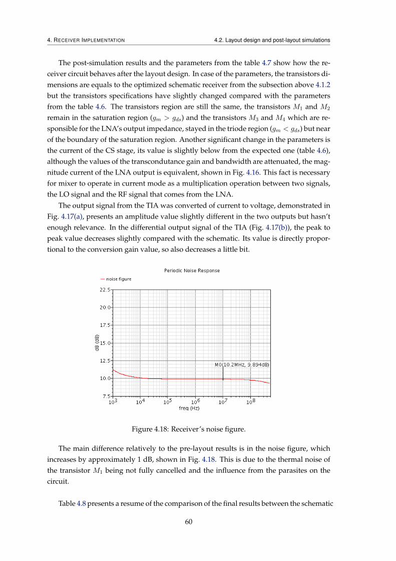
4. RECEIVER IMPLEMENTATION 4.2. Layout design and post-layout simulations
The post-simulation results and the parameters from the table 4.7 show how the re-ceiver circuit behaves after the layout design. In case of the parameters, the transistors di-mensions are equals to the optimized schematic receiver from the subsection above 4.1.2but the transistors specifications have slightly changed compared with the parametersfrom the table 4.6. The transistors region are still the same, the transistors M1 and M2
remain in the saturation region (gm > gds) and the transistors M3 and M4 which are re-sponsible for the LNA’s output impedance, stayed in the triode region (gm < gds) but nearof the boundary of the saturation region. Another significant change in the parameters isthe current of the CS stage, its value is slightly below from the expected one (table 4.6),although the values of the transcondutance gain and bandwidth are attenuated, the mag-nitude current of the LNA output is equivalent, shown in Fig. 4.16. This fact is necessaryfor mixer to operate in current mode as a multiplication operation between two signals,the LO signal and the RF signal that comes from the LNA.
The output signal from the TIA was converted of current to voltage, demonstrated inFig. 4.17(a), presents an amplitude value slightly different in the two outputs but hasn’tenough relevance. In the differential output signal of the TIA (Fig. 4.17(b)), the peak topeak value decreases slightly compared with the schematic. Its value is directly propor-tional to the conversion gain value, so also decreases a little bit.
Figure 4.18: Receiver’s noise figure.
The main difference relatively to the pre-layout results is in the noise figure, whichincreases by approximately 1 dB, shown in Fig. 4.18. This is due to the thermal noise ofthe transistor M1 being not fully cancelled and the influence from the parasites on thecircuit.
Table 4.8 presents a resume of the comparison of the final results between the schematic
60

4. RECEIVER IMPLEMENTATION 4.3. Discussion
and post-layout.
Table 4.8: The schematic and layout simulations results.
Tech Voltage NF IIP3 Power VDD
(nm) Conversion (dB) (dBm) (mW) supplyGain (dB) (V)
Schematic 130 31.5 <8.7 -1.35 1.9 0.6Layout 130 30.9 <9.9 N/A 1.86 0.6
4.3 Discussion
There are several classic RF receiver architectures with different complexities and perfor-mances. However, only some of them are suited for low-power applications, namely theLow-IF or direct conversion architectures. In order to integrate with an energy harvestingpower supply, the receiver has to be designed taking into account the low supply voltagerequirements. In terms of low supply voltage, the design and optimization of the LNAmodule was important for having a successfull reduction of the VDD voltage supply forthe proposed circuit, set at 0.6 V, which is half of the value of the supply voltage thatserved as a starting point for the original LNA, presented in [21].
A double-balanced passive mixer is designed in conjunction with the LNA to workin current mode, allowing a good linearity. Moreover, the passive mixer does not influ-ence the overall power consumption. Also, the receiver circuit doesn’t include the localoscillator and OTA designs, considering them as ideal devices. Although it has a simpleinductorless architecture with reduced area and cost, its design’s simplicity results in alow Power Supply Rejection Ratio (PSRR).
This receiver’s proposed circuit presents a post-layout power consumption value of1.89 mW, which refers to the consumption of the two blocks, the LNA and mixer. Thepower consumption value is calculated through the sum of the currents flowing fromthe two LNA’s stages, which are 1.63 mA and 1.47 mA, shown in table 4.7, and thenmultiplied by the VDD supply voltage.
The receiver’s simple architecture is suitable for modulation schemes with reducedcomplexities. Therefore, the modulation scheme chosen for the proposed receiver front-end circuit was the on/off keying (OOK). The OOK modulation is the most basic modu-lation, which is widely used in close-range communications, low data-rate and low-costapplications. The architecture simplicity and the requirements for the target applicationlead to the choice of the previously mentioned simple modulation scheme [32].
For all that, in order to have sense of the typical power consumption and supply volt-ages of other receivers for WSN applications, some examples are presented in table 4.9.The parameters given in table 4.9, are the technology, the type of modulation scheme, thesupply voltage and the power consumption. The chosen receiver examples presented in
61

4. RECEIVER IMPLEMENTATION 4.3. Discussion
the table work with simple modulation schemes, thus allowing a relevant comparison.
Table 4.9: Comparison of WSN receivers.
Parameters [5] [33] [34] [35] [36] This work
Technology (nm) 90 130 180 130 180 130Modulation OOK OOK FSK FSK OOK OOKSupply Voltage (V) - 1 1 1.2-1.5 1.4 0.6Power Consumption (mW) 1.8 0.88-2.5 2.17 1.92-2.4 0.5-2.6 1.86
62

5Conclusion and Future Work
5.1 Conclusion
In this thesis a CMOS low-power and low-voltage RF receiver designed in a standardCMOS technology was presented. It has an inductorless wideband architecture with areduced area and a consequently reduced cost. The circuit is suitable for the target ap-plication, in which the power is intended to be supplied by an energy harvesting source.The specification requirements for this energy-autonomous WSAN, where the piezoelec-tric energy harvesting was chosen as its power source, are the power consumption andsupply voltage.
This work was validated through the design and implementation of the key circuitblocks, where the theoretical analyses, the behaviour, the characteristics, the parame-ters and the simulations were presented. Despite of the receiver circuit simplicity, theresults obtained in conversion gain, noise factor, linearity and power consumption areacceptable. Therefore, the solution presented in this work is suitable to cope with therequirements of energy-autonomous WSAN application.
The proposed circuit includes the implementation of a wideband balun LNA ableto cancel noise and distortion, working at 0.6 V supply voltage, and a double-balancedpassive mixer which is designed in conjunction with the LNA, to work in current mode.Also, together with the implementation of LNA and mixer, the LO and TIA modules helpto achieve the results of a total voltage conversion gain of 31.5 dB, an IIP3 value of -1.35dBm, and a noise figure lower than 9 dB. The total power consumption achieved is 1.9mW and the total circuit area is 305x134.5 µm2.
Moreover, the simulation results of the implemented circuit are compared with theresults from the post-layout simulations, which show that the concept may be optimized
63

5. CONCLUSION AND FUTURE WORK
and future research can lead to promising results.
5.2 Future Work
In the present work there are always changes and improvements that can be made, whichwould make this project more competitive. The following topics are suggested for im-provement of future work that fall outside the scope of this thesis.
The implementation and design of this project obtained reasonable values of param-eters and dimensions for the work application. However, in the layout phase some prob-lems appeared in the current mirror transistors. The LNA’s current source was not con-sidered as an ideal current source, and a current mirror was added, implemented withstandard 130 nm CMOS transistors. Nonetheless, some problems occurred with the post-layout version of the current mirror for the post-layout simulations. This is the reasonwhy the current mirror was only used in its schematic version, for both types of sim-ulations. A plausible change would be to modify the current mirror transistors for RFtransistors. However, their characteristics and dimensions would be different, since theyhave different models. The most immediate consequence of this change would be in thenoise figure of the proposed circuit, which would increase slightly.
Furthermore, the receiver includes two ideal modules, which are the local oscillatorand the TIA. As future work, an interesting extension of the proposed receiver would beto include the previously mentioned ideal modules in the system design, paying attentionto the requirements for the WSN application.
After the full design and implementation of the proposed RF receiver, the inclusionof the RF transmitter could be considered.
Another suggestion is to design the proposed circuit in a lower CMOS technology toinvestigate if a better compromise between cost, area, power, and performance could beachieved.
A solution for a WSAN receiver whose power is supplied by an energy harvestingsolution is presented in this thesis. The next step in the WSAN co-design consists invalidating the joint operation of the two systems, with the goal of integrating them in aWSAN system-on-chip (SoC).
64

Bibliography
[1] D. M. Pozar. Microwave Engineering. Fourth. John Wiley and Sons Ltd, 2011.
[2] T. Ytterdal, Y. Cheng, and T. A. Fjeldly. Device Modeling for Analog and RF CMOSCircuit Design. John Wiley and Sons Ltd, 2003.
[3] J. C. Whitaker. The Electronics Handbook. Second. Taylor and Francis Group, 2005.
[4] B. Razavi. RF Microelectronics. Prentice-Hall, 1998.
[5] L. Huang, V. Pop, R. de Francisco, R. Vullers, G. Dolmans, H. de Groot, and K. Ima-mura. “Ultra Low Power Wireless and Energy Harvesting Technologies - An IdealCombination”. In: IEEE International Conference on Communication Systems (ICCS)(2010), pp. 295–300.
[6] J. Correia, N. Mancelos, and J. Goes. “Stability improvements in a Rail-to-Rail In-put/Output, constantGm Operational Amplifier, at 0.4 V operation, using the low-voltage DTMOS technique”. In: 5th Doctoral Conference on Computing, Electrical andIndustrial Systems (DoCEIS) 423 (2014), pp. 585–591.
[7] N. Mancelos, J. Correia, L. M. Pires, L. B. Oliveira, and J. P. Oliveira. “Piezoelec-tric energy harvester for a CMOS wireless sensor”. In: 5th Doctoral Conference onComputing, Electrical and Industrial Systems (DoCEIS) 423 (2014), pp. 470–477.
[8] J. Correia, N. Mancelos, L. B. Oliveira, and J. P. Oliveira. “A Low-Voltage LNA andCurrent Mode Mixer Design for Energy Harvesting Sensor Node”. In: MIXDES’14.MIXDES-21th International Conference (2014), pp. 523–528.
[9] N. Mancelos, J. Correia, J. P. Oliveira, and L. B. Oliveira. “Co-design of a Low-power RF Receiver and Piezoelectric Energy Harvesting Power Supply for a Wire-less Sensor Node”. In: International Journal of Microelectronics and Computer Science(2014).
[10] K. Iniewski. VLSI Circuits for Biomedical Applications. Artech House, 2008.
[11] L. B. Oliveira, J. R. Fernandes, I. M. Filanovky, C. J. Verhoeven, and M. M. Silva.Analysis and Design of Quadrature Oscillators. Springer, 2008.
65

BIBLIOGRAPHY
[12] T. H. Lee. The Design of CMOS Radio-Frequency Integrated Circuits. Second. Cam-bridge Univertiy Press, 2004.
[13] D. Leenaerts, J. van der Tang, and C. S. Vaucher. Circuit Design for RF transceivers.Kluwer Academic Publishers, 2001.
[14] A. Grebennikov. RF and Microwave : Transistor Oscillator Design. John Wiley andSons Ltd, 2007.
[15] S. A. Saleh, M. Ortmanns, and Y. Manoli. “A Comparative Study of CMOS LNAs”.In: IEEE 18th European Conference on Circuit Theory and Design (Aug. 2007), pp. 76–79.
[16] J. Ferreira, I. Bastos, L. Oliveira, J. Oliveira, T. Michalak, P. Pankiewicz, B. Nowacki,and P. Makosa. “LNA, Oscillator and Mixer Co-Design for Compact RF-CMOS ISMReceivers”. In: MIXDES’09. MIXDES-16th International Conference (2009), pp. 291–295.
[17] M. de Medeiros Silva. Circuitos Com Transistors Bipolares e MOS. Fundação CalousteGulbenkian, 2006.
[18] A. Amer, E. Hegazi, and H. Ragai. “A Low-Power Wideband CMOS LNA forWiMAX”. In: IEEE Transactions on Circuits and Systems 54 (Jan. 2007), pp. 4–8.
[19] S. C. Blaakmeer, E. A. M. Klumperink, D. M. W. Leenaerts, and B. Nauta. “Wide-band Balun-LNA with Simultaneous Output Balancing, Noise-Canceling and Distortion-Canceling”. In: IEEE Journal of Solid-State Circuits 43 (June 2008).
[20] R. Bagheri, A. Mirzaei, S. Chehrazi, M. Heidari, M. Lee, M. Mikhemar, W. Tang,and A. Abidi. “An 800-MHz-6-GHz Software-Defined Wireless Receiver in 90-nmCMOS”. In: IEEE Journal Of Solid-State Circuits 41.12 (2006), pp. 2860–2876.
[21] I. Bastos, L. B. Oliveira, J. Goes, and M. Silva. “MOSFET-Only Wideband LNA withNoise Cancelling and Gain Optimization”. In: MIXDES’10. MIXDES-17th Interna-tional Conference (June 2010), pp. 306–311.
[22] E. Ortigueira, I. Bastos, L. B. Oliveira, J. P. Oliveira, and J. Goes. “A SimplifiedDesign of a MOSFET-only Wideband Gilbert Cell”. In: MIXDES’11. MIXDES-18th
International Conference (June 2011), pp. 225–230.
[23] M. Krcmar and G. Boeck. “A bradband folded Gilbert cell CMOS mixer”. In: AnalogIntegrated Circuits and Signal Processing 64 (2010), pp. 39–44.
[24] C. Song, O. Boric-Lubecke, and I. Lo. “0.18-µM CMOS WIDEBAND PASSIVE MIXER”.In: Microwave and Optical Technology Letters 55 (2012), pp. 23–27.
[25] F. Assaderaghi, S. Parke, D. Sinitsky, J. Bokor, P. K. Ko, and C. Hu. “A DynamicThreshold Voltage MOSFET (DTMOS) for Very Low Voltage Operation”. In: IEEEElectron Device Letters 15.12 (1994).
66

BIBLIOGRAPHY
[26] F. Assaderaghi, D. Sinitsky, S. Parke, J. Bokor, P. K. Ko, and C. Hu. “DynamicThreshold-Voltage MOSFET (DTMOS) for Ultra-Low Voltage VLSI”. In: IEEE Trans-actions On Electron Devices 44.3 (1997).
[27] S. C. Blaakmeer, E. A. M. Klumperink, D. M. W. Leenaerts, and B. Nauta. “TheBLIXER, a Wideband Balun-LNA-I/Q-Mixer Topology”. In: IEEE Journal Of Solid-State Circuits 43.12 (2008).
[28] R. Bagheri, A. Mirzaei, S. C. M. E. Heidari, M. Lee, M. Mikhemar, W. Tang, and A. A.Abidi. “An 800-MHz-6-GHz software-defined wireless receiver in 90-nm CMOS”.In: IEEE Journal Of Solid-State Circuits 41.12 (2006), pp. 2860–2876.
[29] P. Mak and R. Martins. “Design of an ESD-Protected Ultra-Wideband LNA in NanoscaleCMOS for Full-Band Mobile TV Tuners”. In: IEEE Transactions on Circuits and Sys-tems I 56 (2009), pp. 933–942.
[30] A. Hastings. The Art of Analog Layout. 2001.
[31] N. H. E. Weste and K. Eshraghian. Principles of CMOS VLSI design: A systems per-spective. Second. 1993.
[32] C. Enz, N. Scolari, and U. Yodprasit. “Ultra Low-Power Radio Design for WirelessSensor Networks”. In: IEEE International Workshop on Radio-Frequency IntegrationTechnology (2005), pp. 1–17.
[33] S. Kim, H. Kim, and H. Shin. “A 2.4-GHz CMOS Single-Chip OOK Transceiver forWireless Sensor Network Applications”. In: (2012).
[34] S. Mikami, T. Matsuno, M. Yoshimoto, and H. Ono. “A Wireless-Interface SoC Pow-ered by Energy Harvesting for Short-range Data Communication”. In: Asian Solid-State Circuits Conference (2005), pp. 241–244.
[35] R. van Langevelde, M. van Elzakker, D. van Goor, H. Termeer, J. Moss, and A.J. Davie. “An Ultra-Low-Power 868/915 MHz RF Transceiver for Wireless SensorNetwork Applications”. In: Radio Frequency Integrated Circuits Symposium (2009),pp. 113–116.
[36] D. C. Daly and A. P. Chandrakasan. “An Energy-Efficient OOK Transceiver forWireless Sensor Networks”. In: IEEE Journal of Solid-State Circuits 42.5 (2007), pp. 1003–1011.
67

BIBLIOGRAPHY
68

APublished Papers
69

A. PUBLISHED PAPERS
Stability improvements in a Rail-to-RailInput/Output, constant Gm OperationalAmplifier, at 0.4 V operation, using the
low-voltage DTMOS technique
5th Doctoral Conference on Computing, Electrical and Industrial Systems (DoCEIS)
70

Stability improvements in a Rail-to-Rail Input/Output,
constant Gm Operational Amplifier, at 0.4 V operation,
using the low-voltage DTMOS technique
Joana Correia2, Nuno Mancelos
2, João Goes
1,2
1 Centre for Technologies and Systems (CTS) – UNINOVA 2 Dept. of Electrical Engineering (DEE), Universidade Nova de Lisboa (UNL)
Campus FCT/UNL, 2829-516, Caparica, Portugal [email protected], [email protected], [email protected]
Abstract. The use of the dynamic threshold MOS (DTMOS) technique is
evaluated in a two-stage rail-to-rail Input/Output, constant amplifier. The
proper choice of specific transistors in which the technique should be used is
presented, as well as the resulting improvements, mainly regarding stability of
the circuit at low voltage operation. The DTMOS technique is used in the
NMOS transistors of the folded-cascode input stage, allowing the circuit to be
stable at VDD = 0.4 V, with equivalent gain and gain-and-bandwidth product
(GBW) values achieved with the same value, for the initial circuit
operating at 0.8 V. The implemented changes allow the circuit to be stable at
low voltage operations without requiring any increase in the cascoded-Miller
compensation capacitors, saving circuit area and, consequently, cost.
Keywords: Low-voltage DTMOS technique; Low supply voltage OPAMP;
Low-voltage OPAMP stability issues.
1 Introduction
The general tendency for reducing the supply voltage in ICs represents a challenge
for analog amplifier designers, in terms of maintaining required gain levels,
bandwidth (BW) and stability. In terms of stability and frequency compensation,
several techniques can be implemented, but the solutions represent an increase of the
circuit area, since they often include the need of additional capacitors.
As a starting point for the testing of the DTMOS technique, an operational
transconductance amplifier (OTA) was chosen. The choice is based on an original,
rail-to-rail Input/Output, constant OTA, described in [1], and operating at a 0.8 V
supply. The technology used for the initial amplifier was the purely-digital 180 nm
CMOS, whereas the present implementation, fully supported in the initial study, [1],
was simulated using the CADENCE, with an UMC 130 nm, purely-digital, CMOS
technology. The change in technology doesn’t represent a relevant factor in the
overall behavior of the circuit.
The main objective of this work is to improve the gain, GBW and stability of the
original amplifier, and to guarantee that the OTA still works, with reasonable
performance, when operating at much lower supply voltages.

The DTMOS technique was the technique chosen to reach the objectives, and
consists in connecting the bulk of a transistor to its gate terminal. This allows the bulk
voltage to be variable, instead of being fixed at ground or VDD (NMOS or PMOS,
respectively) [2]. The transistor suffers from body-effect, in this configuration, since
the voltage between the source and bulk terminals is not zero. However, the
transcondutance that is a result of the body-effect contributes, positively, to the total
transcondutance of the transistor, being this contribution an increase of approximately
20-to-30% of the transcondutance of the transistor. This means that in the DTMOS
configuration, the body-effect of a transistor is not a degrading factor in its , but
rather an improvement.
The disadvantages of using the DTMOS technique are the increase of the parasitic
capacitances in the transistor, which can ultimately lead to a loss of circuit BW, and
the possibility of a latch-up problem. In the case of this particular application and
circuit, the latch-up situation is not a real problem, because there won’t be sufficient
voltage to trigger the effect, since the intended test supply voltages will be lower than
0.7 V, which is the typical problematic threshold that allows that effect to be a
problem. In terms of the increase of the parasitic capacitances, and consequent
decrease in BW, the situation can be dealt with separately, although the changes in the
parasitic capacitances are not relevant enough to reflect some problematic difference
in terms of the BW.
2 Relationship to Collective Awareness Systems
Collective Awareness Systems that are capable of harnessing collective
intelligence, allowing the creation of a network of distributed knowledge and data
from real environments, include a multitude of individual subsystems that must be
able to collect and transmit the actual information that is shared in the system. These
subsystems may include a wide range of different devices and applications, but they
usually consist in wireless and portable devices [3] for which concerns like power
consumption and autonomous lifetime are very pertinent.
The DTMOS low voltage technique used in this work is one of the techniques that
allow reduction in circuit supply voltage, and consequently power consumption.
Moreover, as it will be demonstrated in this paper, the use of DTMOS in certain
specific devices can improve the stability of the circuit, which translates into smaller
area (there is no need for larger compensating capacitors). The significant supply
voltage reductions that can be achieved with this technique are promising for the
hardware implementations of Collective Awareness Systems or any other system
where power consumption and cost (silicon area) are key factors.

3 Amplifier Description
3.1 Initial Amplifier
The 0.8 V, rail-to-rail Input/Output, constant OTA, whose schematic is
presented in Fig. 1, consists of two stages.
Fig. 1. Initial Operational Amplifier
The rail-to-rail folded-cascode input stage includes two differential pairs in
parallel, consisting of the transistors M1, M2 (NMOS differential pair), M3 and M4
(PMOS). This configuration allows rail-to-rail operation at the input. For high
common-mode voltages at the input, the NMOS differential pair is on, while for low
common-mode voltages it is the PMOS differential pair that is on. For medium levels
of the common-mode voltages, both differential pairs are on, increasing the current
flowing to the summing circuit and consequently increasing the . To avoid this
increase in the transcondutance, since it is desirable to have it constant for the whole
range of common-mode voltages, the current switches M5 to M8 are added. The
following folded-cascode configuration is responsible for the summing of the signals
(current) coming from the complementary differential pairs.
The class AB output stage features, as stated above, the cascaded-Miller frequency
compensation technique, which includes the capacitors CM1 and CM2. Class AB
operations are made possible by M19 and M20. These transistors are driven by the
signal currents coming from transistors M14 and M16 and are polarized by the diode-
connected transistors M22, M23, M25 and M26. The output transistors M27 and M28
are in common-source configuration to allow rail-to-rail operations at the output. The
M27 transistor functions at the positive swing, while M28 takes care of the negative
swing. The frequency of non-dominant pole is shifted to higher frequencies by the
cascoded-Miller frequency compensation technique.

3.2 Proposed Modifications in the Original Amplifier
The low-voltage DTMOS technique was chosen as the approach to use because of
the simplicity of the implementation, since it basically consists in disconnecting the
bulks of the PMOS and NMOS devices, respectively from and VSS, and re-
connect them to the gate terminal [4, 5].
Many possible configurations have been simulated and evaluated, using the
DTMOS technique applied to different sets of transistors. The best results, taking into
account simplicity and gain results, were achieved using the DTMOS technique only
in the NMOS cascode devices M13 and M14. Notice that the DTMOS technique also
has the benefit of reducing the threshold voltage of the transistor. Since NMOS
transistors have a higher threshold voltage than PMOS, it is understandable that it is
preferable to use the DTMOS technique in the NMOS cascode transistors rather than
in the PMOS. This requires fabrication processes either with triple-well or with deep-
Nwell but this is clearly the case, for all state-of-the-art deep nano-scale CMOS
technologies.
4 Amplifier Performance
4.1 Electrical Simulations of the Original Amplifier Circuit
The simulation results achieved with the initial configuration of the circuit ported
into the 130 nm CMOS technology (the original circuit, without the use of the
DTMOS technique) are presented in Table 1. The presented results include
simulations run under different supply voltages, focusing on the values of DC gain,
GBW and Phase Margin (PM).
Table 2. Simulated results for the initial configuration of the amplifier circuit.
VDD (V) Gain (dB) GBW (kHz) Phase Margin (⁰)
1.2 82.62 857 > 56
0.8 82.58 864 > 56
0.7 81.16 824 > 56
0.6 81.44 833 52
0.5 78.5 818 56
0.4 72.15 878 53
0.3 57.7 794 51
The simulated PM is evaluated at a typical closed-loop gain of 6 dB, for each
value. The presented PM results are lower than 55 o, which leads to the conclusion
that the circuit is not stable for any of these supply voltages. In terms of DC gain and
GBW, the values decrease as a consequence of the lowering of the value, as it is
expected. However, the decrease in those values is not as substantial as was
estimated, revealing that the topology of the circuit is capable of maintaining both the

gain and the GBW performance parameters even at lower supply voltages (i.e., below
0.8 V).
4.2 Re-Design of the Amplifier using DTMOS
For the circuit amplifier including the proposed changes, the same simulations
have been carried-out, under the same conditions (common-mode voltages at 55 % of
, the PM measured with a closed-loop gain of 6 dB). The results are summarized
in Table 2.
Table 2. Results for the new circuit configuration (DTMOS).
VDD (V) Gain (dB) GBW (kHz) Phase Margin (⁰)
1.2 80.37 887 > 60 (higher)
0.8 79.54 844 > 60 (higher)
0.7 79.14 902 (higher) > 60 (higher)
0.6 79.5 872 (higher) 57 (higher)
0.5 77.14 909 (higher) 61 (higher)
0.4 72.45 (higher) 924 (higher) 60 (higher)
0.3 58.82 (higher) 794 (same) 59 (higher)
As it can be observed in Table 2, there are just minor improvements in the DC gain
and in the GBW. The most significant improvement is the PM parameter, particularly
at very low supply voltages below 0.6 V. Since the values are superior to 55o, the
OTA circuit is now stable for those values and can operate down to 0.3 V.
The gain and phase plots are presented in Fig. 2 and in Fig. 3, for a 0.4 V supply
voltage. This value was chosen as a reference example because it is half the value
of the supply voltage for which the original circuit was designed (which constitutes,
by itself, a significant reduction in the supply voltage) and because it presents good
gain, GBW and PM results, in comparison to the results achieved by the original
circuit, for that same .

Fig. 3. Gain trace.
Fig. 3. Gain and Phase traces.

5 Conclusions
It has been demonstrated in this paper that, using DTMOS in a couple of specific
devices of a two-stage rail-to-rain Input/Output, constant Gm OTA can improve its
stability whilst operating at very low supply voltages. The proper choice of specific
transistors in which the technique should be used has been presented, as well as the
resulting improvements. The implemented changes allow the circuit to be stable at
low voltage operations without requiring any increase in the cascoded-Miller
compensation capacitors, saving circuit area and, consequently, cost.
The significant supply voltage reductions that can be achieved with this DTMOS
technique are, therefore, quite promising for the hardware implementations of
Collective Awareness Systems, in which amplifiers are of paramount importance, and
where power consumption and cost (silicon area) are limiting factors.
References
1. J. Citakovic, I. Riis Nielsen, J. Hammel Nielsen, P. Asbeck, and P. Andreani: A 0.8V, 7μA,
Rail-to-Rail Input/Output, Constant Gm Operational Amplifier in Standard Digital 0.18μm
CMOS. In: IEEE Xplore, pp.54-57, Denmark (2005).
2. Shouri Chatterjee, K. P. Pun, Nebojša Stanić, Yannis Tsividis and Peter Kinget: Analog
Circuit Design Techniques at 0.5V. Springer (2007).
3. Nicola Bicocchi, Damiano Fontana, Marco Mamei and Franco Zambonelli: Collective
Awareness and Action in Urban Superorganisms, Italy (2013).
4. Somayeh Abdollahvand and João Goes: Design of Robust CMOS Amplifiers Combining
Advanced Low-Voltage and Feedback Techniques. In: Doctoral Conference on Computing
Electrical and Industrial Systems (DoCEIS’2012). Caparica, Portugal: DEE/FCT/UNL,
2012.
5. Somayeh Abdollahvand, Rui Santos-Tavares and João Goes: A Low-Voltage CMOS Buffer
for RF Applications Based on a Fully-Differential Voltage-Combiner. In: Doctoral
Conference on Computing, Electrical and Industrial Systems (DoCEIS’2013). Caparica,
Portugal: IFIP Advances in Information and Communication Technology, 2013.

A. PUBLISHED PAPERS
Piezoelectric energy harvester for a CMOSwireless sensor
5th Doctoral Conference on Computing, Electrical and Industrial Systems (DoCEIS)
78

Piezoelectric energy harvester for a CMOS wireless
sensor
Nuno Mancelos 2, Joana Correia
2, Luís Miguel Pires
1,2, Luís B. Oliveira
1,2 and
João P. Oliveira 1,2
1 Centre for Technologies and Systems (CTS) – UNINOVA 2 Dept. of Electrical Engineering (DEE), Universidade Nova de Lisboa (UNL)
Campus FCT/UNL, 2829-516, Caparica, Portugal [email protected], [email protected], [email protected], [email protected]
Abstract. The emerging of collective awareness platforms opened a new range
of driven forces that will converge to more sustainable systems. To achieve this
task, these platforms have to support an increasing number of more
sophisticated remote sensors and actuators that will need to cooperate smartly
and strongly with each other in a mesh type of intelligent interconnectivity.
These remote smart miniaturized nodes can add noninvasive intelligence but
suffer from lifetime performance due to the small quantity of energy available
in micro batteries. Therefore, harvesting energy from the environment is a
promising technique. This work presents the study and experimental evaluation
of a flexible piezoelectric material to validate the use of a piezoelectric
harvester in a CMOS wireless actuator/sensor node.
Keywords: Energy harvesting, piezoelectric transducers, self-powered,
micro-systems, smart systems, wireless sensor nodes, MEMS, WSN
1. Introduction
The recent advances in ultra-low-power device integration, communication
electronics and Micro Electro-Mechanical Systems (MEMS) technology have fuelled
the emerging technology of Wireless Sensor Networks (WSNs). The spatial
distributed nature of WSNs often requires batteries to power the individual sensor
nodes. One of the major limitations on performance and lifetime of WSNs is the
limited capacity of these finite power sources, which must be manually replaced when
they are depleted. Moreover, the embedded nature of some of the sensors and
hazardous sensing environment make battery replacement very difficult and costly.
The process of harnessing and converting ambient energy sources into usable
electrical energy is called energy harvesting. Energy harvesting raises the possibility
of self-powered systems, which are ubiquitous and truly autonomous, and without
human intervention for energy replenishment. Among the ambient energy sources
such as solar energy, heat, and wind, mechanical vibrations are an attractive ambient
source mainly because they are widely available and are ideal for the use of
piezoelectric materials, which have the ability to convert mechanical strain energy
into electrical energy.

Contributions of this paper are summarized as follows. Section 2 presents the
relationship to Collective Awareness Systems. In Section 3, state of the art of energy
harvesting transducers are presented. In Section 4 the concept of synergy between
piezoelectric energy harvesters and WSN is justified and a block diagram of the
proposed self-powered Wireless Actuator/Sensor Node is presented. Section 5
presents experimental evaluation of the piezoelectric harvester. Finally some
conclusions are drawn in section 6.
2. Relationship to Collective Awareness Systems
Nowadays, the emergence of collective awareness systems is pushing the
performance of end user interactive objects. The support framework based in a
interconnected objects and things (IoT) is the bridge that combines technologies and
components from micro-systems (miniaturized electric, mechanical, optical and fluid
devices) with knowledge, technology and functionality from several areas of research.
However, Harbor Research [1] defines smart systems as a new generation of
systems architecture (hardware, software, network technologies, and manage services)
that provides real-time awareness based on inputs from machines, people, video
streams, maps, new feeds, sensors and more that integrate people, process, and
knowledge to enable collective awareness and decision making.
WSN provide endless opportunities, but at the same time pose formidable
challenges, such as the fact that energy is a scarce and usually non-renewable
resource. However, as part of WSN, micro-systems could provide advances in low
power VLSI, embedded computing, communication hardware, and in general, the
convergence of computing and communications, are making this emerging
technology a reality. Likewise, advances in nanotechnology and MEMS are pushing
toward networks of tiny distributed sensors and actuators.
As mentioned in the previous section, energy harvesting can dramatically extend
the operating lifetime of nodes on WSN. Finally, this technology enables battery less
operation and reduces the operation costs of WSN, which are mainly due to battery
replacement.
3. Energy Harvesting from the surroundings
Energy harvesting techniques developed for micropower generators deal with the
challenge of scavenging and making use of residual energy present in ambient
sources, usually energy in the form of light, radio RF electromagnetic radiation,
thermal gradients and many sources of motion, namely rotation, vibration and fluid
flow. Energy harvesting transducers that make use of energy in the form of motion are
called Electromechanical and are separated in three different groups: electromagnetic,
electrostatic and piezoelectric transducers. Piezoelectric transducers make use of the
piezoelectric effect, which refers to the accumulation of an electrical charge in some
solid materials, like crystals and certain ceramics, when a mechanical stress is applied
to them. The effect is reversible, which means that movement, in the form of
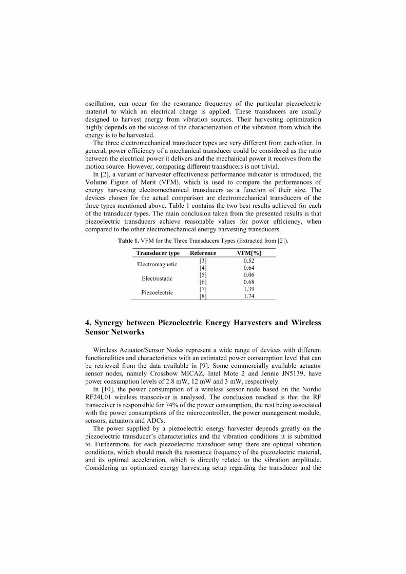
oscillation, can occur for the resonance frequency of the particular piezoelectric
material to which an electrical charge is applied. These transducers are usually
designed to harvest energy from vibration sources. Their harvesting optimization
highly depends on the success of the characterization of the vibration from which the
energy is to be harvested.
The three electromechanical transducer types are very different from each other. In
general, power efficiency of a mechanical transducer could be considered as the ratio
between the electrical power it delivers and the mechanical power it receives from the
motion source. However, comparing different transducers is not trivial.
In [2], a variant of harvester effectiveness performance indicator is introduced, the
Volume Figure of Merit (VFM), which is used to compare the performances of
energy harvesting electromechanical transducers as a function of their size. The
devices chosen for the actual comparison are electromechanical transducers of the
three types mentioned above. Table 1 contains the two best results achieved for each
of the transducer types. The main conclusion taken from the presented results is that
piezoelectric transducers achieve reasonable values for power efficiency, when
compared to the other electromechanical energy harvesting transducers.
Table 1. VFM for the Three Transducers Types (Extracted from [2]).
Transducer type Reference VFM[%]
Electromagnetic [3] 0.52
[4] 0.64
Electrostatic [5] 0.06
[6] 0.68
Piezoelectric [7] 1.39
[8] 1.74
4. Synergy between Piezoelectric Energy Harvesters and Wireless
Sensor Networks
Wireless Actuator/Sensor Nodes represent a wide range of devices with different
functionalities and characteristics with an estimated power consumption level that can
be retrieved from the data available in [9]. Some commercially available actuator
sensor nodes, namely Crossbow MICAZ, Intel Mote 2 and Jennie JN5139, have
power consumption levels of 2.8 mW, 12 mW and 3 mW, respectively.
In [10], the power consumption of a wireless sensor node based on the Nordic
RF24L01 wireless transceiver is analysed. The conclusion reached is that the RF
transceiver is responsible for 74% of the power consumption, the rest being associated
with the power consumptions of the microcontroller, the power management module,
sensors, actuators and ADCs.
The power supplied by a piezoelectric energy harvester depends greatly on the
piezoelectric transducer’s characteristics and the vibration conditions it is submitted
to. Furthermore, for each piezoelectric transducer setup there are optimal vibration
conditions, which should match the resonance frequency of the piezoelectric material,
and its optimal acceleration, which is directly related to the vibration amplitude.
Considering an optimized energy harvesting setup regarding the transducer and the

characterisation of the vibration frequency, the circuit responsible for rectification and
eventual voltage supply regulation must be designed and implemented. It should be
noted that this circuit has a power efficiency associated to it. As an optional
component in the power management part of the system, and depending, once again,
on the vibration predictability, an energy storage device might be considered.
Two examples of piezoelectric energy harvesters implemented with optimal
vibration characteristics and resistive loads that maximize the power output are given
in [9] and [11]. In the first case, a power output of 3 mW was achieved, while in the
second work a value of 4.4 mW was also experimentally verified. For the first
implementation, a Volture V22BL piezoelectric transducer was used, with vibration
characteristics of 50 Hz and 1g. The second example makes use of a Piezo Systems
T226-A4-503X piezoelectric transducer, with vibration characteristics of 50 Hz and
0.5 g. It should be noted that the power outputs are achieved using optimized resistive
loads for each of the situations.
Although power consumption and power output levels do not match, energy
harvesting solutions can be made possible using a duty cycling technique, making use
of a battery or a supercapacitor. This technique consists in switching periodically the
sensor node on and off. Since the wireless sensor node doesn’t have to be constantly
communicating, the energy harvested by the transducer is used in the communication
time interval of the sensor node and stored in the battery (or capacitor) during the rest
of the cycle (switched off time interval). In [2], a duty cycle of 1.6% is used for a
solution using a piezoelectric energy harvester powering a custom designed radio
transceiver that requires 12 mW when transmitting. The power consumption values
previously presented, from [9], are based in operating conditions of 1%
communication, 10% processing and 89% sleeping. The proposed block diagram of a
self-powered actuator/sensor node is presented in Figure 1.
Figure 1. Block diagram of a Piezoelectric-powered WSN.

5. Experimental Evaluation of the Piezoelectric Energy Harvester
The chosen piezoelectric energy harvester Midé Volture™ V21bl [12], designed
for vibration energy harvesting, is presented in Figure 2. It uses the piezoelectric
characteristics of its specific piezoceramic material to produce electrical charge when
mechanically stimulated [13] and consists in a package of piezoelectric materials in a
protective skin, with four pre-attached electrical leads.
Figure 2. Midé Volture™ V21bl [12]. Figure 3. Parallel equivalent circuit.
The piezoelectric harvester includes two electrically isolated piezo wafers, which
may be used independently or in one of two possible combinations. These
combinations can be optimised for increased output voltage (series configuration) or
increased output current (parallel configuration). For this implementation, and since
the desired output voltage is relatively low compared to the range of typical output
voltages of the piezoelectric harvester, the parallel configuration is used, in order to
maximize the output current needed to charge the capacitor. Figure 3 presents the
final equivalent circuit of the parallel configuration of the two wafers.
A block diagram of the test setup is shown in Figure 4, which comprises three
complementary parts:
1. a test vibration module which is formed by an audio amplifier (LM386) and
vibration speaker coupled to the piezoelectric transducer;
2. a rectifying diode bridge plus a fast charge capacitor;
3. a data-acquisition subsystem, consisting of a 10-bit ADC and a MCU
connected to both a LCD Module (HD44780 module, 16X2 LCD Panel) and
a USB connection to a computer.
Figure 4. Block diagram of the test setup.
A picture taken of the test setup is shown in Figure 5.

The energy stored in the capacitor is calculated using the standard equation given
by,
. (1)
For the Energy calculation, the actual capacitance of the parallel of capacitors was
set to 2100 μF. In fact, this energy was calculated using the discharge time of the
capacitor (from 1.3 V to 0 V), which is approximately 21 seconds, Figure 6 a). Using
this discharge time, the resistance value of the RC circuit (2 KΩ) and the RC time
constant approximation, the actual capacitance of the capacitor can be calculated.
Using this value, the estimated stored energy in the capacitor is 1.77 mJ, for 1.3 V.
Figure 5. Photograph of the implementation.
Two different methods of vibration were used during the tests: the manually
induced and the one produced by the small amplitude vibration speaker. The optimal
vibration frequency was found for the second case.
For the manually induced movement test, a constant oscillation frequency was
emulated. Given the equivalent circuit of the piezoelectric harvester, previously
presented in Figure 3, the expected behaviour of the charging circuit is described by,
(
) (2)
where is the instant voltage across the capacitor while depends on the open
circuit voltage of the piezoelectric harvester. The charging time was approximately 68
seconds, Figure 6 b). After some testing using a speaker, the optimal vibration
frequency for energy harvesting purposes was found to be 58 Hz. Three tests were run
with this vibration frequency, following the same procedure. The charging process
was interrupted when the capacitor reached 1.3 V, after which the capacitor is
connected to a 2 kΩ resistor. Figure 6 a) shows the results of these three tests.

Figure 6. a) Three tests for the optimal vibration frequency – 58 Hz; b) manually induced
movement test.
The charging time of the capacitor (from 0 V to 1.3 V) is approximately 125
seconds (medium value). It is greater than the one achieved with the first test (the
manually induced movement test), proving that the tip-to-tip displacement amplitude,
related to the vibration acceleration, is an important factor in the energy harvesting
implementation, using this particular piezoelectric energy harvester.
Using non-optimal vibration frequencies for the vibration speaker case, the time
the piezoelectric harvester takes to charge the capacitor up to the same voltage level is
greater. To prove this, two non-optimal frequencies were chosen: 60 Hz, which is
above the optimal frequency, and 56 Hz, which is below. The charging times for these
tests are approximately 250 seconds for the first one and 180 seconds for the second.
Both of them are greater than the one achieved for the optimal vibration frequency,
125 seconds. Table 2 shows practical results of this work.
Table 2. Summary of the experimental results.
Vibration type Vibration
frequency
Charging
time (from
0V to 1.3V)
Energy stored in
the capacitor
after charging
time
Capacitor used
Vibration Speaker
58 Hz 125 s
1.77 mJ 2100 μF 56 Hz 180 s
60 Hz 250 s
Manual - 68 s
6. Conclusions
The main conclusion of the present work is that it is possible to implement an
energy harvesting solution using the piezoelectric energy harvester Midé Volture™
V21bl for low voltage applications, even if the vibration conditions applied to the
harvester are not optimal. Comparing the vibration speaker case and the test involving

manually induced oscillation, it is possible to conclude that the tip-to-tip displacement
amplitude is a very important factor in terms of energy generated by the piezoelectric
device, more so than the actual selection of the right frequency for the oscillation.
For each configuration of the mechanical vibration method, there is an optimal
vibration frequency, for energy harvesting purposes. In the case of this
implementation, that frequency is approximately 58 Hz.
7. References
[1] Harbor Research: Machine-to-Machine (M2M)a dn Smart Systems Forecast 2010-2014, Harbor Research 2010.
[2] Paul D. Mitcheson, Eric M. Yeatman, G. Kondala Rao, Andrew S. Holmes and Tim C. Green: Energy Harvesting From Human and Machine Motion for Wireless Electronic Devices. In: Paul D. Mitcheson, vol. 96, No. 9, September 2008.
[3] N. N. H. Ching, H. Y. Wong, W. J. Li, P. H. W. Leong and Z. Wen: A laser-micromachined vibrational to electrical power transducer for wireless sensing systems. In: Proc. 11th Int. Conf. Solid-State Sensors Actuators, Munich, Germany, Jun. 2001.
[4] N. N. H. Ching, H. Y. Wong, W. J. Li, P. H. W. Leong and Z. Wen: A laser-micromachined multi-modal resonating power transducer for wireless sensing systems. Sensors Actuators A, Phys., vol. 97-98, pp. 685-690, Apr. 2002.
[5] G. Despesse, J. Chaillout, T. Jager, J. M. Léger, A. Vassilev, S. Basrour and B. Charlot: High damping electrostatic system for vibration energy scavenging. In: Proc. 2005 Joint Conf. Smart Objects Ambient Intell. – Innov. Context-Aware Services: Usages Technol., pp. 283-286, Grenoble, France, 2005.
[6] Y. Arakawa, Y. Suzuki and N. Kasagi: Micro seismic electrets generator using electrets polymer film. In: Proc. 4th Int. Workshop Micro and Nanotechnology for Power Generation and Energy Conversion Applicat. Power MEMS, pp. 187-190, Kyoto, Japan, (Nov. 2004).
[7] H. B. Fang, J. Q. Liu, Z. Y. Xu, L. Dong, L. Wang, D. Chen, C. Bing-Chu and Y. Liu: Fabrication and performance of MEMS-based piezoelectric power generator for vibration energy harvesting. In: Microelectron, J., vol. 37, no. 11, pp. 1280-1284, 2006.
[8] S. Roundy, P. K. Wright and J. M. Rabaey: Energy scavenging for wireless sensor networks. 1st ed. Boston, MA: Kluwer Academic, 2003.
[9] Yong-Jin Yoon, Woo-Tae Park, King Ho Holden Li, Yu Qi Ng and Yongnam Song: A Study of Piezoelectric Harvesters for Low-Level Vibrations in Wireless Sensor Network. In: International Journal of precision engineering and manufacturing Vol. 14, No. 7, Seul (July 2013).
[10] Li Huang, Valer Pop, Ruben de Francisco, Ruud Vullers, Guido Dolmans, Harmke de Groot and Koji Imamura: Ultra Low Power Wireless and Energy Harvesting Technologies – An Ideal Combination. In: IEEE , Eindhoven, The Netherlands and Osaka, Japan, 2010.
[11] Dao Zhou, Na Kong, Dong Sam Ha, and Daniel J. Inman: A Self-powered Wireless Sensor Node for Structural Health Monitoring. In: Health Monitoring of Structural and Biological Systems, Blacksburg, USA, 2010.
[12] Datasheet: Midé: PIEZOELECTRIC ENERGY HARVESTERS. VoltureTM.
[13] Datasheet: Volture Products - Material Properties. Volture Products - Material Properties,VoltureTM

A. PUBLISHED PAPERS
A Low-Voltage LNA and Current Mode MixerDesign for Energy Harvesting Sensor Node
IEEE Mixed Design of Integrated Circuits and Systems (MIXDES)
87

A Low-Voltage LNA and Current Mode Mixer Design for Energy Harvesting Sensor Node
Joana Correia, Nuno Mancelos, João P. Oliveira, Luís B. Oliveira
CTS-UNINOVA, Department of Electrical Engineering (DEE), Faculty of Sciences and Technology (FCT), Universidade Nova de Lisboa
Monte da Caparica, Portugal ([email protected], [email protected], [email protected], [email protected])
Abstract—A low-voltage RF CMOS receiver front-end for energy harvesting Wireless Sensor Node (WSN) is presented. A MOSFET-only wideband balun LNA, with noise and distortion cancelling, is designed to work at 0.6 V supply voltage, in conjunction with a passive mixer. The passive mixer works in current mode, allowing a minimal introduction of noise and a good linearity. The receiver front-end reaches a total voltage conversion gain of 31.5 dB, a 0.1-5.2 GHz bandwidth, an IIP3 value of -1.35 dBm, and a noise figure inferior to 32.6 dB. The total power consumption is 1.95 mW.
Index Terms—CMOS RF analog front-end; Low-power and low-voltage RF receiver; Low-voltage wideband balun LNA; Double-balanced passive mixer; RF receiver for Wireless Sensor Networks.
I. INTRODUCTION Low-power receiver architectures used in analog front-end
transceiver circuits are a good option to consider when overall consumption is a key factor. This is the case for Wireless Sensor Node Networks (WSN), where individual sensor nodes, Wireless Sensor Actuator Nodes (WSAN), must be energetically autonomous and communicate wirelessly with each other, sharing information regarding physical measurements of their environment made by their sensors and eventually sharing commands destined to their actuators, [1].
The Low-IF receiver architecture features down-conversion to an intermediate frequency that is high enough to avoid problems related with flicker noise (that are a concern in zero-IF or direct conversion architectures) and low enough to relax the filter specifications associated with channel selection, [2]. Figure 1 represents the block diagram of the chosen architecture. This architecture allows a good performance at low-power consumption, which is the main constraint of the target application.
Since the wireless sensor nodes must be energetically autonomous and battery replacement increase maintenance costs, Energy Harvesting (EH) techniques are a very promising solution to power these nodes. Among existing EH techniques, piezoelectric power source was chosen, [3].
This paper presents a CMOS low-voltage RF receiver front-end making use of Low-IF receiver architecture, designed to work with simple binary modulations such as OOK modulation, [4] and at a supply voltage of only 0.6 V. The circuit was designed and simulated using CADENCE, with a 130 nm, purely-digital, CMOS technology.
Figure 1. Low-IF Receiver Architecture.
The low-power consumption is possible due to a careful sizing of the transistors, the inclusion of a low-voltage technique in the LNA’s first stage and the implementation of a passive mixer. Moreover, a Dynamic Threshold voltage MOS (DTMOS) technique, [5], was also implemented in order to further reduce the operating supply voltage.
Section II presents a selection of state-of-the-art LNA and mixer circuits. The complete proposed circuit including the LNA and mixer is presented in section III. Section IV includes some implementation considerations regarding transistor dimensioning and biasing voltages, as well as power consumption values. Section V presents the simulations run for the proposed circuit, including gain, noise figure and linearity. A Figure of Merit is calculated and used to compare the proposed circuit to other state-of-the-art receiver solutions. The comparison includes positive and negative characteristics of the proposed receiver. Finally, some conclusions are presented in section VI.
II. WIDEBAND BALUN LNAS AND MIXER CIRCUITS
A. Wideband Balun LNAs The wideband balun LNA presented in [6], and depicted in
Fig. 2 has a common-gate (CG) and a common-source (CS) stage, a single-ended, unbalanced input and delivers a balanced output, thus guaranteeing the balun functionality. It is able to cancel the noise of the first stage, the CG-stage, as long as both stages have the same gain. This happens because the first stage’s noise appears as a common-mode signal at the differential output. Dimensioning CG and CS devices with different sizes and bias allows this circuit to simultaneously benefit from noise and distortion cancelation and the output
This work was supported by national funds through FCT - Portuguese Foundation for Science and Technology under projects PEst-OE/EEI/UI0066/2011 and DISRUPTIVE (EXCL/EEI-ELC/0261/2012).

balancing abilities, as is demonstrated in [6]. The circuit can achieve very good linearity as long as the CS-stage’s linearity is assured.
Figure 2. Wideband Balun LNA, [6].
A MOSFET-only version of the previously referred LNA circuit is presented in [7], Fig. 3. This version replaces the CG and CS resistors (used in [6]) by PMOS transistors M3 and M4, respectively, operating in the triode region but close to saturation, allowing an increase of the incremental load resistance and, consequently, to the LNA’s gain, for the same DC voltage drop. The replacement of the resistors by the PMOS devices also results in a reduction of circuit area and cost. Regarding the original LNA, this circuit has the disadvantage of an increased distortion and a reduction of bandwidth.
Figure 3. MOSFET-only Wideband Balun LNA [7].
B. Mixer circuits The simplest mixer configuration is a CMOS transistor-
implemented switch, whose gate is driven by the Local Oscillator (LO) signal, with the RF signal being applied at its
drain and the Intermediate Frequency (IF) signal being taken at its source. This passive mixer has no DC consumption and provides high linearity and bandwidth, [8].
Active mixers provide gain and strengthen the IF signal as they deliver it to subsequent receiver stages. They are most commonly based on the differential pair and can be single-balanced or double-balanced, depending on whether the RF signal coming from the LNA is balanced or unbalanced.
The single-balanced active mixer has a differential pair with the inputs driven by the LO signals and a current source controlled by the RF unbalanced signal. The two sides of the differential pair convert the RF input voltage to a current that is drawn alternately. For this mixer, the output spectrum includes the LO frequency. It is a simple active mixer that has moderate gain and noise figure, high input impedance and low 1 dB compression point, low IIP3 and low port-to-port isolation [8].
The double-balanced active mixer, called Gilbert cell, is more complex, having LO and RF differential inputs. It features improvements when compared to the single-balanced active mixer, namely higher gain, lower noise figure, high port-to-port isolation and good linearity. It is also able to remove the LO frequency from the output spectrum. These improvements come at the cost of higher consumption and increased circuit area and cost. [1,8]
III. COMPLETE PROPOSED CIRCUIT Fig. 4 presents the complete implemented circuit, including
the LNA, mixer, DC decoupling capacitors between those two and the transimpedance amplifier (TIA) after the mixer, which is able to buffer the final output, filter frequencies higher than the chosen IF frequency and convert the current signal to a voltage signal. Between the mixer and the TIA a DC voltage source is added as a common-mode voltage of the two TIA inputs. The design of the TIA block is not detailed in this paper and the OTA is considered to reach a gain of 1000.
The main contribution of the presented circuit is not the introduction of new LNA and mixer architectures but rather a new implementation of their combination: the signals are treated in current mode. The RF signal coming from the antenna is converted to current and amplified by the LNA, being delivered to the mixer as a balanced signal. The mixer’s output, a balanced current signal IF, is then converted to a balanced voltage signal by the TIA.
A. LNA The proposed LNA circuit is presented in Fig. 4, along with
the rest of the receiver analog front-end designed in the present work. This LNA is a new version of the MOSFET-only LNA presented in section II, designed to work at a supply voltage of 0.6 V. With a careful dimensioning, the use of a low-voltage technique and the introduction of independent stage biasing, the LNA is able to work without losing too much of its gain, as will be shown in sections IV and V. Since the dimensions of the PMOS devices can be adjusted to increase the LNA’s output resistance, the current output of the LNA can be optimised. This is an important factor because the chosen mixer operates in current mode. Consequently, the LNA’s

voltage gain is not the main concern, but rather its transcondutance gain, which is essentially given by the M1 (CG) and M2 (CS) gm values.
The VDD reduction is possible due to an additional biasing voltage applied to the CS stage (Vbias2), to guarantee enough gate-source voltage across transistor M2. Since Vbias1 is limited to the supply voltage value, it wouldn’t be sufficient to assure both M1 and M1 VGS needed values. For this reason, Vbias2 was added, along with the decoupling capacitor C1.
Additionally, the DTMOS low-voltage technique is used in transistor M1 to allow the low supply voltage operation. The technique consists in connecting the bulk of the transistor to its gate terminal [5], introducing a dynamic regulation of the transistor’s threshold voltage. The use of this technique allows enough drain-source voltage for the current-source transistor. It does so by reducing the threshold voltage of transistor M1. The DTMOS technique is also responsible for a small increase in the effective gm of device M1, slightly contributing to the CG voltage gain. This consideration is included in the LNA’s differential voltage gain expression, (1), presented in this section. LNA differential voltage gain
The expression for the LNA differential voltage gain is achieved by the subtraction of the CG and CS voltage gains, which were deduced using a small signal incremental model of the LNA. The gain if given by
𝐴𝑉 !"## =!"!!!"#!!!"#!!!"!
!!"!!!!"!!!"!!!!"!
!!"!!!!"! (1)
which can be approximated by
𝐴𝑉 !"## ≈!"!!!"#!!!"!
!!"!!!!"! . (2)
The presented approximation is valid considering that gds1 and gds2 have similar values, the same happening for gds3 and gds4.
LNA input-impedance
The LNA input-impedance is given by (3).
𝑍!" =!"#!!!"#!
!"!!!"#!!!"#! !!"! (3)
LNA noise figure
Assuming that 𝑔!! = 𝑔!! = 𝑔!, the noise figure is given by (4) [6, 7].
𝐹!"# = 1 + !!!!"!!!!"!!"
!!!!!
+ !!!!!
+ !!!!!!
+ !!!!!"!!!
(4)
with 𝑘 as the Boltzmann’s constant, 𝑐′!" the oxide gate capacitance per unit area, 𝑊! and 𝐿! the transistor dimensions, 𝑇 the absolute temperature, 𝛾 the excess noise factor, 𝑘! and 𝛼! intrinsic process parameters.
B. Mixer The choice of the mixer architecture for the receiver was
governed once again by the energy consumption constraint of the target application. Since this factor is critical for the overall functioning of the WSAN receiver, a passive mixer architecture was chosen. The circuit is presented in Fig. 4 and consists of two pairs of NMOS transistors used as voltage-controlled switches, working in the triode zone to maintain a low drain-source voltage when turned ON. The RF signal at the mixer’s input is mixed in current. For a passive mixer as this one, the LO signals must be strong and buffered. The LO signals that drive the devices’ gates are considered as ranging from 0 V to VDD supply voltage, 0.6 V.
The mixer works in current mode, allowing a minimal introduction of noise and a good linearity. The reduced noise introduction, especially flicker noise, is possible due to the inclusion of the DC decoupling capacitors between the LNA and mixer, which guarantee there is no DC current flowing through the mixer. Moreover, due to the TIA, the variation of the drain-source voltage of the mixer’s NMOS is reduced, thus contributing to improve the linearity of the circuit.
Figure 4. Complete Receiver Circuit with all transistor sizes (W/L) in µm.

C. Theoretical expressions of the complete circuit Assuming that 𝑔!! = 𝑔!! = 𝑔! and R4 = R5, the noise
figure is given by (7) [6, 7].
𝐹!"#$% = 1 + !!!!"!!!!"!!"
!
!!!!+ !
!!!!+ !
!!!!!+ !
!!!!!!! (7)
The overall conversion gain is given by
𝐶𝐺!"#$% = 𝐺𝑚!"#×𝑍!"# !"#$%& @ !"!"# . (8)
IV. CIRCUIT IMPLEMENTATION The design process began by defining the VDD voltage and
power consumption values. Vbias1 was set to 0.6 V and Vbias2 at 0.45 V. A current mirror, biasing the first stage of the LNA with a current value of approximately 1.64 mA, designed the current source. The common-mode voltage at the TIA input is set at 100 mV.
The circuit was dimensioned to work with an RF frequency of 1 GHz and an IF of 10 MHz. The LO frequency was considered as 990 MHz. For simulation purposes, the oscillator signals, LO+ and LO– in Fig. 4, were considered square waves in quadrature, with 50 ps of rise and fall times and without overlapping, with peak-to-peak buffered voltages of 0.6 V.
The NMOS and PMOS transistors chosen are RF transistors, with a triple-well structure chosen for the NMOS. Their dimensions are presented in Table I. The chosen length (L) for all the transistors was the technology’s minimum L value, in this case 120 nm, in order to maximize circuit speed. To define the width for M1, (3) was considered, so that this device’s dimensions would guarantee 50 Ω input matching. Widths of M3 and M4 were determined by the LNA’s output impedance, which means that these values were chosen with the objective of setting the PMOS drain-source resistances at a desired value, initially 200 Ω. The optimised value for the width of M2 was chosen as the one which allowed the CS gain to match the CG gain, a required condition for the noise cancelling capability, as explained in section II. This matching of the CG and CS gains was possible after the optimization process applied to size M2. The chosen width values for the mixer devices were set with the objective of achieving small drain-source resistance values.
The resistor and capacitor values chosen are presented in Table II. Resistor R1 limits the DC current generated by Vbias2 and resistors R2 and R3 help setting the common-mode voltage at the TIA input. Capacitor C1 is responsible for the DC decoupling between the two LNA stages and capacitors C2 and C3 allow the DC decoupling between the LNA and mixer, while achieving low impedance values at the RF frequency of interest. Resistor values of R4, R5 and capacitor values of C4 and C5 are chosen so that a low pass filter is implemented at the TIA. The cutoff frequency of the filter was dimensioned to be slightly higher than the IF frequency, in order to attenuate frequencies above IF. The TIA’s transresistance gain value, responsible for the current to voltage conversion, is 200 KΩ for the IF frequency (10 MHz). This value corresponds to the
impedance of the parallel of resistor R5 and capacitor C4 (or R4 and C5) for the given IF frequency.
TABLE I. TRANSISTOR DIMENSIONS TABLE FOR THE LNA AND MIXER
𝐼!
(𝑚𝐴) W
(µm) L
(µm) 𝑟!" (𝛺)
𝑔!" (𝑚𝑆)
𝑔! (𝑚𝑆)
LNA
𝑀! 1.64 66 0.12 453 2.2 20.15 𝑀! 1.63 75.6 0.12 576 1.73 21.88 𝑀! 1.64 52.8 0.12 254 3.93 8.6 𝑀! 1.63 53.28 0.12 257 3.89 8.5
Mixer 𝑀!,!,!,! - 115.2 0.12 - - -
TABLE II. RESISTOR AND CAPACITOR DIMENSIONS
R1,R2,R3
(kΩ) R4,R5 (kΩ)
C1,C2,C3 (ρF)
C4,C5 (ρF)
Values 10 200 5 9
V. SIMULATION RESULTS
A. Selection of simulations run For the IIP3 simulation, shown in Fig. 5, the tones are 100
MHz apart from each other, a situation that would be ideal for an IF frequency value of 100 MHz. Even though this is not the chosen IF frequency, the results achieved with this value is also illustrative for a 10 MHz IF case. The simulation was run using a tone separation frequency value different from the desired IF frequency for reasons concerning simulation and convergence times. The IIP3 simulation renders a value of -1.35 dBm.
In order to validate the low noise capabilities of the complete circuit, a noise figure simulation, shown in Fig. 6, was run for the differential IF output. The simulation’s results lead to the conclusion that the circuit presents a low noise figure, around 8.6 dB, for a relatively wide band of frequencies close to the desired IF frequency.
Figure 5. IIP3 simulation.

Figure 6. Noise Figure simulation.
B. Results Table The FoM expression considered is presented in (9). In order
to calculate the FoM values, gain and NF were converted from the dB values presented in Tables III and IV.
𝐹𝑜𝑀 mW!! =!" !"##
!"!! !!"[!"] (9)
For comparison purposes, the same FoM expression was used to calculate the state-of-the-art circuits’ FoM values.
Table III presents the final results for this work’s presented
circuit. These results include LNA bandwidth, LNA differential voltage gain, LNA FoM, and some results for the complete circuit, namely conversion gain, noise figure, IIP3 and power consumption.
TABLE III. FINAL RECEIVER SIMULATION RESULTS
Tech (nm)
LNA LNA + Mixer
Band (GHz)
Gain (dB)
Voltage Conversion Gain (dB)
NF (dB)
IIP3 (dBm)
Power (mW)
VDD Supply
(V)
130 0.1-5.2 17.6 31.5 <8.57 -1.35 1.95 0.6
C. FoM results and comparison with state-of-the-art circuits A comparison with state-of-the-art LNAs is presented in
Table IV. The LNA was chosen for comparison because it is the most critical block in terms of gain and distortion in the receiver presented circuit.
TABLE IV. COMPARISON WITH STATE-OF-THE-ART LNAS.
Ref. Tech (nm)
VDD (V)
Band (GHz)
Gain (dB)
NF (dB)
IIP3 (dBm)
Power (mW)
FoM (mW-1)
[6] 65 1.2 0.2-5.2 15.6 <3.5 >0 14 0.34
[9] 90 2.5 0.8–6 20 <3.5 >-3.5 12.5 0.6
[10] 90 1.2 0.1–1.9 20.6 <2.7 10.8 9.6 1.3
[11] 130 1.2 0.2–3.8 11.2 <2.8 -2.7 1.9 2.1
[7] 130 1.2 0.2–6.6 19.8 <1.8 1.6 4.8 3.9 This
Work 130 0.6 0.1–5.2 17.6 <5.2 2.3 1.95 1.7
D. Results discussion The circuit’s bandwidth satisfies the requirements for the
target application. The LNA’s voltage gain value is equivalent to the voltage gain value of the original MOSFET-only LNA that was considered, which is a positive result, having in mind the VDD voltage supply reduction for the proposed circuit, in relation to the original one. The voltage conversion gain of the complete circuit is a result of the contribution of the LNA’s gain and the TIA’s gain. The transimpedance gain of the TIA has a large contribution in this total conversion gain. The noise figure result is slightly higher than the LNA’s noise figure, meaning that the mixer introduces some noise but not as much as an active mixer would. The IIP3 has a satisfactory value due to the reduced distortion introduced by the LNA and mixer.
E. Positive and negative characteristics of the proposed circuit The main advantages of the proposed circuit are its low-
power and low-voltage operation, its simplicity, good linearity and wideband operation, all of which are important factors for the target application. The introduction of noise is also reduced, thanks to the noise cancellation capability of the LNA and the fact that the receiver includes a passive mixer working in current mode. Moreover, it is an inductorless circuit, which helps in the reduction of the overall circuit area and, for that reason, circuit cost.
As a disadvantage, this work’s receiver does not include the
oscillator and the OTA designs, considering them as ideal devices. Additionally, and as a consequence of its simplicity, the circuit presents a low Power Supply Rejection Ratio (PSRR). Another disadvantage is the need for LO signal drivers.
VI. CONCLUSIONS
The CMOS ultra low-power and low-voltage RF receiver design includes the implementation of a MOSFET-only wideband balun LNA able to cancel noise and distortion, working at 0.6 V supply voltage, with a bandwidth of 0.1-5.2 GHz, a voltage gain of 17.6 dB, a noise figure inferior to 5.2 dB and an IIP3 value of 2.3 dBm. A double-balanced passive mixer is designed in conjunction with the LNA, working in current mode, and guaranteeing, together with the LNA and transimpedance amplifier (TIA), a total voltage conversion gain of 31.5 dB, an IIP3 value of -1.35 dBm, and a noise figure inferior to 32.6 dB. The total power consumption achieved is 1.95 mW.
The proposed receiver presents a good solution for a Wireless Sensor Actuator Node (WSAN) receiver whose power is supplied by an Energy Harvesting solution, mainly due to its low-power consumption, which is a critical factor for an energy-autonomous WSAN. This receiver has a simple inductorless architecture, resulting in a reduced area and, consequently, reduced circuit cost.

REFERENCES [1] K. Iniewski, “VLSI Circuits for Biomedical Applications,” Artech House,
2008. [2] J. Crols and M. Steyaert, “CMOS Wireless Transceiver Design”, Kluwer,
1997. [3] N. Mancelos, J. Correia, L. M. Pires, L.B. Oliveira, and J. P. Oliveira,
“Piezoelectric energy harvester for a CMOS wireless sensor”, 5th
Doctoral Conference on Computing, Electrical and Industrial Systems (DoCEIS), Portugal, 2014.
[4] C. C. Enz, N. Scolari, U. Yodprasit, “Ultra Low-Power Radio Design for Wireless Sensor Networks”, IEEE International Workshop on Radio-Frequency Technology, Singapore, 2005.
[5] J. Correia, N. Mancelos, and J. Goes, “Stability improvements in a rail-to-rail input/output, constant gm operational amplifier, at 0.4V operation, using the low-voltage DTMOS technique”, 5th Doctoral Conference on Computing, Electrical and Industrial Systems (DoCEIS), Portugal, 2014.
[6] S. Blaakmeer, E. Klumperink, D. Leenaerts, and B. Nauta, “Wideband Balun-LNA with Simultaneous Outputs Balancing, Noise-Canceling and Distortion-Canceling”, IEEE J. Solid-State Circuits, vol. 43, no. 6, pp. 1341-1350, June 2008.
[7] I. Bastos, L.B. Oliveira, J. Goes, M. Silva, "MOSFET-only wideband LNA with noise cancelling and gain optimization," IEEE Mixed Design of Integrated Circuits and Systems (MIXDES), 2010, pp.306-311, 24-26 June 2010.
[8] L. Oliveira, J. R. Fernandes, I. M. Filanovsky, C. J. M. Verhoeven and M. M. Silva, “Analysis and Design of Quadrature Oscillators”, Springer, 2008.
[9] R. Bagheri, A. Mirzaei, S. Chehrazi, M. E. Heidari, M. Lee, M. Mikhemar, W. Tang, and A. A. Abidi, “An 800-MHz–6-GHz software-defined wireless receiver in 90-nm CMOS,” IEEE J. Solid-State Circuits, vol. 41, no. 12, pp. 2860–2876, Dec. 2006.
[10] P.-I. Mak and R. Martins, “Design of an ESD-Protected Ultra-Wideband LNA in Nanoscale CMOS for Full-Band Mobile TV Tuners”, IEEE Trans. Circuits Systems I, vol. 56, pp. 933-942, May 2009.
[11] A. Amer, E. Hegazi, and H. Ragai, “A low power wideband CMOS LNA for WiMax”, IEEE Trans. Circuits Systems. II, vol. 54 nº 1, pp. 4-8, Jan. 2007.

A. PUBLISHED PAPERS
Co-design of a Low-power RF Receiver andPiezoelectric Energy Harvesting Power Supply for
a Wireless Sensor Node
International Journal of Microelectronics and Computer Science (Invited Paper ofMIXDES 2014)
94

Co-design of a Low-power RF Receiver and
Piezoelectric Energy Harvesting Power Supply for a
Wireless Sensor Node
Nuno Mancelos, Joana Correia, João P. Oliveira, Luís B. Oliveira
CTS-UNINOVA, Department of Electrical Engineering (DEE),
Faculty of Sciences and Technology (FCT), Universidade Nova de Lisboa
Monte da Caparica, Portugal
([email protected], [email protected], [email protected], [email protected])
Abstract—A low-voltage RF CMOS receiver front-end and an
energy harvesting power circuit for a piezoelectric source are
presented as a co-designed solution for a Wireless Sensor Node. A
MOSFET-only wideband balun LNA with noise cancelling and a
0.6 V supply voltage is designed in conjunction with a passive
mixer. The passive mixer operates in current mode, allowing a
minimal introduction of voltage noise and a good linearity. The
receiver front-end reaches a total voltage conversion gain of 31
dB, a 0.1-5.2 GHz bandwidth, an IIP3 value of -1.35 dBm, and a
noise figure inferior to 9 dB. The total power consumption is 1.95
mW. The energy harvesting power circuit consists of an active full
bridge cross-coupled rectifier followed by a low-dropout (LDO)
regulator, and it is able to guarantee a power output of 6 mW
with a regulated output voltage of 0.6 V, for typical vibration
patterns.
Index Terms—CMOS RF analog front-end; Low-voltage
wideband balun LNA; Passive mixer; Piezoelectric Energy
Harvesting; Active full bridge rectifier; LDO regulator.
I. INTRODUCTION
Low-power receiver architectures used in analog front-end
transceiver circuits are a good option to consider when overall
consumption is a key factor. This is the case for Wireless
Sensor Networks (WSN), where individual sensor nodes,
Wireless Sensor Actuator Nodes (WSAN), must be
energetically autonomous and communicate wirelessly with
each other, sharing information regarding physical
measurements of their environment made by their sensors and
eventually sharing commands destined to their actuators, [1].
The Low-IF receiver architecture features down-conversion
to an intermediate frequency that is high enough to avoid
problems related with flicker noise (that are a concern in the
direct conversion architecture) and low enough to relax the
filter specifications associated with channel selection, [2]. This
architecture allows a good performance at low-power
consumption, which is the main constraint of the target
application.
Since the wireless sensor nodes must be energetically
autonomous and battery replacement increases maintenance
costs, Energy Harvesting (EH) techniques are a very promising
solution to power these nodes. Among existing EH techniques,
a piezoelectric power source was chosen, [3], with the residual
energy source to be scavenged contained in ambient vibrations.
Piezoelectric transducers are essentially ceramic wafers that
exhibit piezoelectricity. This property consists in the creation
of electrical charge in piezoelectric materials when they suffer
mechanical strains, and it is reversible, meaning that an applied
electrical field results in internal mechanical strain. When
subjected to vibration, these transducers create a varying output
voltage that must be rectified and regulated, in order to meet
the application’s power requirements. The scavenged energy
can then be stored with a supercapacitor. Figure 1 presents a
block diagram for the overall approach, including the Low-IF
receiver architecture.
Figure 1. Block diagram for this work’s co-designed approach; Low-IF
Receiver Architecture.
This work presents a CMOS low-voltage RF receiver front-
end, which is designed to operate at a supply voltage of only
0.6 V and for simple binary modulations, such as OOK
modulation, [4]. The low-power consumption is possible due to
a careful sizing of the transistors, the inclusion of low-voltage
techniques in the LNA and the implementation of a passive
mixer. The Dynamic Threshold voltage MOS (DTMOS)
technique, [5], was implemented in order to further reduce the
operating supply voltage. This work was supported by national funds through FCT - Portuguese Foundation for
Science and Technology under projects PEst-OE/EEI/UI0066/2011 and DISRUPTIVE
(EXCL/EEI-ELC/0261/2012).

The EH power circuit, designed to power the RF receiver,
includes an active full bridge cross-coupled rectifier that
rectifies the output of the piezoelectric transducer. After the
rectifier, a low-dropout (LDO) regulator is responsible for
regulating the output of the rectifier to a DC voltage value of
0.6 V, with minimum ripple (<1%). The output of the power
circuit feeds the receiver’s power supply rail.
Section II presents a selection of relevant LNA and mixer
circuits. The receiver proposed circuitry, including the LNA
and mixer, is presented in section III. The piezoelectric EH
system is introduced in Section IV. Section V presents the
simulation results for the receiver, including gain, noise figure
and linearity, and for the EH power circuit. Finally, some
conclusions are presented in section VI.
II. WIDEBAND BALUN LNAS AND MIXER CIRCUITS
A. Wideband Balun LNAs
The wideband balun LNA presented in [6], and depicted in
Fig. 2 has a common-gate (CG) and a common-source (CS)
stage, a single-ended, unbalanced input and delivers a balanced
output, thus guaranteeing the balun functionality. It is able to
cancel the noise of the first stage, the CG-stage, as long as both
stages have the same gain. This happens because the first
stage’s noise appears as a common-mode signal at the
differential output. Dimensioning CG and CS devices with
different sizes and bias allows this circuit to simultaneously
benefit from noise and distortion cancelling and the output
balancing abilities, as is demonstrated in [6]. The circuit can
achieve very good linearity as long as the CS-stage’s linearity
is assured.
Figure 2. Wideband Balun LNA, [6].
A MOSFET-only version of the previously referred LNA
circuit is presented in [7], Fig. 3. This version replaces the CG
and CS resistors (used in [6]) by the PMOS transistors M3 and
M4, respectively, operating in the triode region but close to
saturation, allowing an increase to the incremental load
resistance and, consequently, to the LNA’s gain, for the same
DC voltage drop. The replacement of the resistors by the
PMOS devices also results in a reduction of circuit area and
cost. Regarding the original LNA, this circuit has the
disadvantage of an increased distortion and a reduction of
bandwidth.
Figure 3. MOSFET-only Wideband Balun LNA [7].
B. Mixer circuits
The simplest mixer configuration is a CMOS transistor-
implemented switch, whose gate is driven by the Local
Oscillator (LO) signal, with the RF signal being applied at its
drain and the Intermediate Frequency (IF) signal being taken at
its source. This passive mixer has no DC consumption and
provides high linearity and bandwidth, [8].
Active mixers provide gain and strengthen the IF signal as
they deliver it to subsequent receiver stages. They are most
commonly based on the differential pair and can be single-
balanced or double-balanced, depending on whether the RF
signal coming from the LNA is balanced or unbalanced.
The single-balanced active mixer has a differential pair
with the inputs driven by the LO signals and a current source
controlled by the RF unbalanced signal. The two sides of the
differential pair convert the RF input voltage to a current that is
drawn alternately. For this mixer, the output spectrum includes
the LO frequency. It is a simple active mixer that has moderate
gain and noise figure, high input impedance, low 1 dB
compression point, low IIP3 and low port-to-port isolation [8].
The double-balanced active mixer, called Gilbert cell, is
more complex, having LO and RF differential inputs. It
features improvements when compared to the single-balanced
active mixer, namely higher gain, lower noise figure, high port-
to-port isolation and good linearity. It is also able to remove
the LO frequency from the output spectrum. These
improvements come at the cost of higher consumption and
increased circuit area and cost, [1,8].

III. RECEIVER PROPOSED CIRCUIT
Figure 4 presents the complete circuit, including the LNA,
mixer, DC decoupling capacitors between those two and the
transimpedance amplifier (TIA), which is responsible for
buffering the final output, low-pass filtering, and converting
the current signal to a voltage signal. Between the mixer and
the TIA a DC voltage source is added as a common-mode
voltage of the two TIA inputs. The design of the TIA block is
not detailed in this paper and the OTA is considered to reach a
gain from 500 to 1000.
The main contribution of the presented circuit is not the
introduction of new LNA and mixer architectures but rather the
implementation of the current mode signal processing enabled
by their combination. The RF signal coming from the antenna
is converted to current and amplified by the LNA, being
delivered to the mixer as a balanced signal. The mixer’s output,
a balanced current signal IF, is then converted to a balanced
voltage signal by the TIA.
A. LNA
The proposed LNA circuit is presented in Fig. 4, along with
the rest of the receiver analog front-end designed in the present
work. This LNA is a new version of the MOSFET-only LNA
presented in section II, designed to work at a supply voltage of
0.6 V. With a careful dimensioning, the use of a low-voltage
technique and the introduction of independent stage biasing,
the LNA is able to work without losing too much of its gain, as
will be shown in section V. Since the dimensions of the PMOS
devices can be adjusted to increase the LNA’s output
resistance, the current output of the LNA can be optimised.
This is an important factor because the chosen mixer operates
in current mode. Consequently, the LNA’s voltage gain is not
the main concern, but rather its transcondutance gain, which is
essentially given by the M1 (CG) and M2 (CS) gm values.
The VDD reduction is possible due to an additional biasing
voltage applied to the CS stage (Vbias2), to guarantee enough
gate-source voltage across transistor M2. Since Vbias1 is limited
to the supply voltage value, it wouldn’t be sufficient to assure
both M1 and M2 VGS needed values. For this reason, Vbias2 was
added, along with the decoupling capacitor C1.
Additionally, the DTMOS low-voltage technique is used in
transistor M1 to allow the low supply voltage operation. The
technique consists in connecting the bulk of the transistor to its
gate terminal, [5], introducing a dynamic regulation of the
transistor’s threshold voltage. The use of this technique allows
enough drain-source voltage for the current-source transistor. It
does so by reducing the threshold voltage of transistor M1. The
DTMOS technique is also responsible for a small increase in
the effective gm of device M1, slightly contributing to the CG
voltage gain. This consideration is included in the LNA’s
differential voltage gain expression, (1), presented in this
section.
LNA differential voltage gain
The expression for the LNA differential voltage gain is
achieved by the subtraction of the CG and CS voltage gains,
which were deduced using a small signal incremental model of
the LNA. The gain is given by (1)
| (
)
(1)
which can be approximated by (2).
|
(2)
The presented approximation is valid considering that gds1 and
gds2 have similar values, the same happening for gds3 and gds4.
LNA input-impedance
The LNA input-impedance is given by (3).
( ) (3)
Figure 4. Complete Receiver Circuit with all transistor sizes (W/L) in µm.

LNA noise figure
Assuming that = = , the noise figure is given by (4) [6, 7].
(
)
(4)
with as the Boltzmann’s constant, the oxide gate capacitance per unit area, and the transistor dimensions, the absolute temperature, the excess noise factor, and
intrinsic process parameters.
B. Mixer
The choice of the mixer architecture for the receiver was
governed once again by the energy consumption constraint of
the target application. Since this factor is critical for the overall
functioning of the WSAN receiver, a passive mixer
architecture was chosen. The circuit is presented in Fig. 4 and
consists of two pairs of NMOS transistors used as voltage-
controlled switches, working in the triode region to maintain a
low drain-source voltage when turned ON. The RF signal at the
mixer’s input is mixed in current. For a passive mixer as this
one, the LO signals must be strong and buffered. The LO
signals that drive the devices’ gates are considered as ranging
from 0 V to VDD supply voltage, 0.6 V.
The mixer works in current mode, allowing a minimal
introduction of noise and a good linearity. The reduced noise
introduction, especially flicker noise, is possible due to the
inclusion of the DC decoupling capacitors between the LNA
and mixer, which guarantee there is no DC current flowing
through the mixer. Moreover, due to the TIA, the variation of
the drain-source voltage of the mixer’s NMOS is reduced, thus
contributing to improve the linearity of the circuit.
C. Theoretical expressions of the complete receiver circuit
Assuming that = = and R4 = R5, the noise figure is given by (5) [6, 7].
(
)
(5)
The overall conversion gain is given by (6).
(6)
D. Receiver Circuit Sizing
The design process began by defining the VDD voltage and
power consumption values. Vbias1 was set to 0.6 V and Vbias2 at
0.45 V. A current mirror, biasing the first stage of the LNA
with a current value of approximately 1.64 mA, was included
as the current source. The common-mode voltage at the TIA
input is set at 100 mV.
The circuit was dimensioned to work with an RF frequency
of 1 GHz and an IF of 10 MHz. The LO frequency was
considered as 990 MHz. For simulation purposes, the oscillator
signals, LO+ and LO– in Fig. 4, were considered square waves
in quadrature, with 50 ps of rise and fall times and without
overlapping, with peak-to-peak buffered voltages of 0.6 V.
The NMOS and PMOS transistors chosen are RF transistors,
with a triple-well structure chosen for the NMOS. Their
dimensions are presented in Table I. The chosen length (L) for
all the transistors was the technology’s minimum L value, in
this case 120 nm, in order to maximize circuit speed. To define
the width for M1, (3) was considered, so that this device’s
dimensions would guarantee 50 Ω input matching. Widths of
M3 and M4 were determined by the LNA’s output impedance,
which means that these values were chosen with the objective
of setting the PMOS drain-source resistances at a desired
value, initially 200 Ω. The optimised value for the width of M2
was chosen as the one which allowed the CS gain to match the
CG gain, a required condition for the noise cancelling
capability, as explained in section II. This matching of the CG
and CS gains was possible after the optimization process
applied to size M2. The chosen width values for the mixer
devices were set with the objective of achieving small drain-
source resistance values.
The resistor and capacitor values chosen are presented in
Table II. Resistor R1 limits the DC current generated by Vbias2
and resistors R2 and R3 help setting the common-mode voltage
at the TIA input. Capacitor C1 is responsible for the DC
decoupling between the two LNA stages and capacitors C2 and
C3 allow the DC decoupling between the LNA and mixer,
while achieving low impedance values at the RF frequency of
interest. Resistor values of R4, R5 and capacitor values of C4
and C5 are chosen so that a low pass filter is implemented at
the TIA. The cutoff frequency of the filter was dimensioned to
be slightly higher than the IF frequency, in order to attenuate
frequencies above IF. The TIA’s transresistance gain value,
responsible for the current to voltage conversion, is 200 KΩ for
the IF frequency (10 MHz). This value corresponds to the
impedance of the parallel of resistor R5 and capacitor C4 (or R4
and C5) for the given IF frequency.
TABLE I. TRANSISTOR DIMENSIONS FOR THE LNA AND MIXER
( ) W
(µm) L
(µm) ( )
( )
( )
LNA
1.64 66 0.12 453 2.2 20.15
1.63 75.6 0.12 576 1.73 21.88
1.64 52.8 0.12 254 3.93 8.6
1.63 53.28 0.12 257 3.89 8.5
Mixer - 115.2 0.12 - - -
TABLE II. RESISTOR AND CAPACITOR DIMENSIONS
R1,R2,R3
(kΩ) R4,R5 (kΩ)
C1,C2,C3 (ρF)
C4,C5 (ρF)
Values 10 200 5 9

IV. ENERGY HARVESTING PROPOSED CIRCUIT
Figure 5 presents a block diagram of the EH system,
including the rectifier block, the voltage regulator block and
the Crect and Cstorage supercapacitors. The EH power circuit is
responsible for the conditioning of the piezoelectric
transducer’s power output. This output may be considered as
an AC power signal with a frequency that is equal to the
vibration frequency. This power signal is periodic but not
trivial to emulate, consisting of irregular voltage bursts and
peaks. As an approximation, sine waves were used to simulate
the power source, with the typical amplitude voltage values
given in the datasheet for the Midé Volture™ piezoelectric
transducers family, [9]. These transducer output values were
used as a specification for the ideal voltage source of the
transducer’s equivalent circuit presented in [3], in its Thevenin
equivalent version.
The system was designed to work without batteries, making
use of supercapacitors to store the scavenged energy. These
supercapacitors are external components due to their high
capacitance values, preferably higher than 100 μF. One of
these, Crect, is used at the output of the rectifier and is essential
for the rectification. The Cstorage capacitor serves as the energy
storage device, being placed after the voltage regulator. The
0.6 V regulated output of the system is taken directly at this
capacitor’s terminals.
A. Rectifier
Figure 6. Active Full Bridge Cross-coupled Rectifier Circuit Schematic.
The designed rectifier is an active full bridge cross-coupled
rectifier, containing two NMOS and two PMOS transistors
working as switches with their gates directly driven by the
input terminals of the rectifier. Figure 6 shows the rectifier’s
schematic.
The cross-coupled configuration allows the rectifier to
behave as a full bridge rectifier. Having Fig. 6 as a reference,
this means that transistors N1 and P2 are switched on while the
rectifier’s input is inverted, meaning that the PZT- terminal has
a higher potential than the PZT+ terminal. When the opposite
occurs, transistors N2 and P1 are on, because N2’s gate is
connected to the highest potential and P1’s gate to the lowest.
The rectifier’s output terminals are connected to the Crect
capacitor and the rectifier charges this capacitor because this
output’s polarity is maintained during each period of the input
signal. The anode terminal of the Crect capacitor is called Vrect,
since this is the node with the rectified voltage that needs to be
regulated to a 0.6 V DC value. The cathode terminal represents
the power circuit’s ground.
B. LDO regulator
The LDO regulator acts as a DC-DC converter, regulating
the Vrect output of the rectifier to a DC output at a constant 0.6
V. The output of the LDO regulator, Vout, is therefore
connected to the Cstorage capacitor. The LDO regulator consists
of a PMOS power switch and the comparator that drives the
switch’s gate. A schematic of the LDO regulator is shown in
Fig. 7.
Figure 7. Low-dropout Regulator Schematic.
Figure 5. Block Diagram of the Piezoelectric Energy Harvesting System.
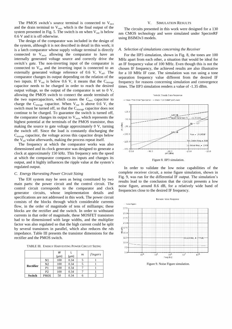
The PMOS switch’s source terminal is connected to Vrect
and the drain terminal to Vout, which is the final output of the
system presented in Fig. 5. The switch is on when Vout is below
0.6 V and it is off otherwise.
The design of the comparator was included in the design of
the system, although it is not described in detail in this work; it
is a latch comparator whose supply voltage terminal is directly
connected to Vrect, allowing the comparator to have an
internally generated voltage source and correctly drive the
switch’s gate. The non-inverting input of the comparator is
connected to Vout and the inverting input is connected to an
externally generated voltage reference of 0.6 V, Vref. The
comparator changes its output depending on the relation of the
two inputs. If Vout is below 0.6 V, it means that the Cstorage
capacitor needs to be charged in order to reach the desired
output voltage, so the output of the comparator is set to 0 V,
allowing the PMOS switch to connect the anode terminals of
the two supercapacitors, which causes the Crect capacitor to
charge the Cstorage capacitor. When Vout is above 0.6 V, the
switch must be turned off, so that the Cstorage capacitor does not
continue to be charged. To guarantee the switch is turned off,
the comparator changes its output to Vrect, which represents the
highest potential at the terminals of the PMOS transistor, thus
making the source to gate voltage approximately 0 V, turning
the switch off. Since the load is constantly discharging the
Cstorage capacitor, the voltage across this capacitor drops below
the Vref value afterwards, making the process repeat itself.
The frequency at which the comparator works was also
dimensioned and its clock generator was designed to generate a
clock at approximately 150 kHz. This frequency sets the speed
at which the comparator compares its inputs and changes its
output, and it highly influences the ripple value at the system’s
regulated output.
C. Energy Harvesting Power Circuit Sizing
The EH system may be seen as being constituted by two
main parts: the power circuit and the control circuit. The
control circuit corresponds to the comparator and clock
generator circuits, whose implementation details and
specifications are not addressed in this work. The power circuit
consists of the blocks through which considerable currents
flow, in the order of magnitude of tens of milliamps; these
blocks are the rectifier and the switch. In order to withstand
currents in that order of magnitude, these MOSFET transistors
had to be dimensioned with large widths, and the multiplier
factor was also regulated so that the high current could be split
by several transistors in parallel, which also reduces the rds
impedance. Table III presents the transistor dimensions for the
rectifier and the PMOS switch.
TABLE III. ENERGY HARVESTING POWER CIRCUIT SIZING
W
(µm) L
(µm)
Rectifier
100 0.34 5 1
100 0.34 5 1
100 0.34 7 1
100 0.34 7 1
Switch 50 0.34 6 2
V. SIMULATION RESULTS
The circuits presented in this work were designed for a 130
nm CMOS technology and were simulated under SpectreRF
using BSIM3v3 models.
A. Selection of simulations concerning the Receiver
For the IIP3 simulation, shown in Fig. 8, the tones are 100
MHz apart from each other, a situation that would be ideal for
an IF frequency value of 100 MHz. Even though this is not the
chosen IF frequency, the achieved results are also illustrative
for a 10 MHz IF case. The simulation was run using a tone
separation frequency value different from the desired IF
frequency for reasons concerning simulation and convergence
times. The IIP3 simulation renders a value of -1.35 dBm.
Figure 8. IIP3 simulation.
In order to validate the low noise capabilities of the
complete receiver circuit, a noise figure simulation, shown in
Fig. 9, was run for the differential IF output. The simulation’s
results lead to the conclusion that the circuit presents a low
noise figure, around 8.6 dB, for a relatively wide band of
frequencies close to the desired IF frequency.
Figure 9. Noise Figure simulation.

Results Table
Table IV presents the final results for this work’s receiver
circuit. These results include LNA bandwidth, LNA
differential voltage gain, and some results for the complete
circuit, namely conversion gain, noise figure, IIP3 and power
consumption.
TABLE IV. FINAL RECEIVER SIMULATION RESULTS
Tech (nm)
LNA LNA + Mixer
Band
(GHz)
Gain
(dB)
Voltage
Conversion Gain (dB)
NF
(dB)
IIP3
(dBm)
Power
(mW)
VDD
Supply (V)
130 0.1-
5.2 17.6 31.5 <8.57 -1.35 1.95 0.6
FoM results and comparison with state-of-the-art circuits
The FoM expression considered is presented in (7). In order
to calculate the FoM values, gain and NF were converted from
the dB values presented in Tables IV and V.
[ ] |
( ) [ ] (7)
For comparison purposes, the same FoM expression was
used to calculate the state-of-the-art circuits’ FoM values. A
comparison with state-of-the-art LNAs is presented in Table V.
The LNA was chosen for comparison because it is the most
critical block in terms of gain and distortion in the receiver
presented circuit.
TABLE V. COMPARISON WITH STATE-OF-THE-ART LNAS.
Ref. Tech
(nm)
VDD
(V)
Band
(GHz)
Gain
(dB)
NF
(dB)
IIP3
(dBm)
Power
(mW)
FoM
(mW-1)
[6] 65 1.2 0.2-5.2 15.6 <3.5 >0 14 0.34
[10] 90 2.5 0.8–6 20 <3.5 >-3.5 12.5 0.6
[11] 90 1.2 0.1–1.9 20.6 <2.7 10.8 9.6 1.3
[12] 130 1.2 0.2–3.8 11.2 <2.8 -2.7 1.9 2.1
[7] 130 1.2 0.2–6.6 19.8 <1.8 1.6 4.8 3.9
This
Work 130 0.6 0.1–5.2 17.6 <5.2 2.3 1.95 1.7
B. Energy Harvesting Power Circuit Simulations
To allow the EH power circuit to supply a fully functional
receiver, an approximation was made for the total power
consumption, and a DC current of 10 mA was considered as
the load’s total requested current, at a 0.6 V supply, which
results in a total estimated power consumption of 6 mW.
For simulation purposes, a load (representing the receiver
front-end) was added to the EH power circuit, consisting in a
current mirror driving a DC current of 10 mA from the output
of the system.
Figure 10 presents a transient simulation of the power
circuit where the Vrect and Vout signals, specified in Fig. 6 and
7, can be seen. This simulation represents the charging process
of the Cstorage capacitor, from which the 10 mA DC current is
requested by the load. The voltage across the Cstorage capacitor,
Vout, is initially 0 V and reaches the 0.6 V value after
approximately 24 ms, for the chosen simulation conditions.
The voltage ripple at the output is below 1%, as can be verified
in the zoomed in section of Fig. 10. The piezoelectric
transducer’s electrical model, in its Thevenin equivalent
version, has its ideal voltage source set to generate a sine wave
with a 5 V amplitude value. The transducer presents a high
internal voltage drop, which is why the rectifier’s output, Vrect,
presents a considerably lower value.
Figure 10. Transient simulation for the Power Supply circuit; Vrect and Vout signals are specified in figures 6 and 7.
C. Results discussion
Regarding the Receiver
The receiver circuit’s bandwidth satisfies the requirements
for the target application. The LNA’s voltage gain value is
equivalent to the voltage gain value of the original MOSFET-
only LNA that was considered, which is a positive result,
having in mind the VDD voltage supply reduction for the
proposed circuit, in relation to the original one. The voltage
conversion gain of the complete receiver circuit is a result of
the contribution of the LNA’s gain and the TIA’s gain. The
transimpedance gain of the TIA has a large contribution in this
total conversion gain. The noise figure result is slightly higher
than the LNA’s noise figure, meaning that the mixer introduces
some noise but not as much as an active mixer would. The IIP3
has a satisfactory value due to the reduced distortion
introduced by the LNA and mixer.
The main advantages of the proposed receiver circuit are its
low-power and low-voltage operation, its simplicity, good
linearity and wideband operation, all of which are important
factors for the target application. The introduction of noise is
also reduced, thanks to the noise cancellation capability of the
LNA and the fact that the receiver includes a passive mixer
working in current mode. Moreover, it is an inductorless
circuit, which helps in the reduction of the overall circuit area
and, for that reason, circuit cost.
A disadvantage of the receiver circuit, which is a
consequence of its simplicity, is its low Power Supply
Rejection Ratio (PSRR). However, this disadvantage has its
consequences taken to a minimum, because the power supply
circuit is designed in order to deliver a strictly regulated
voltage supply.
Regarding the Energy Harvesting Power Circuit
The EH power circuit is capable of guaranteeing a power
output level that not only satisfies the LNA and mixer
modules’ power demands, but eventually the power
requirements of the whole receiver. This is true for power
outputs of the piezoelectric transducer that are relatively
constant and moderately strong, which is a possibility for
certain levels of ambient vibrations. The reduced voltage ripple
at the output (<1%) is a good result, having in mind that,
during the simulation, the load constantly requested a 10 mA
DC current.
VI. CONCLUSIONS
The CMOS low-power and low-voltage RF receiver design
includes the implementation of a MOSFET-only wideband
balun LNA able to cancel noise and distortion, working at 0.6
V supply voltage, with a bandwidth of 0.1-5.2 GHz, a voltage
gain of 17.6 dB, a noise figure inferior to 5.2 dB and an IIP3
value of 2.3 dBm. A double-balanced passive mixer is
designed in conjunction with the LNA, working in current
mode, and guaranteeing, together with the LNA and TIA, a
total voltage conversion gain of 31.5 dB, an IIP3 value of -1.35
dBm, and a noise figure inferior to 9 dB. The total power
consumption achieved is 1.95 mW.
A power consumption of 6 mW is guaranteed by the
designed piezoelectric EH power circuit with an almost self-
sufficient operation, considering that the piezoelectric
transducer is subjected to moderate levels of vibration. This
power supply is able to regulate the required voltage output
with a ripple that is inferior to 1%, which is an important
achievement, having in mind the receiver’s low PSRR.
REFERENCES
[1] K. Iniewski, “VLSI Circuits for Biomedical Applications,” Artech House, 2008.
[2] J. Crols and M. Steyaert, “CMOS Wireless Transceiver Design”, Kluwer, 1997.
[3] N. Mancelos, J. Correia, L. M. Pires, L.B. Oliveira, and J. P. Oliveira, “Piezoelectric energy harvester for a CMOS wireless sensor”, 5th
Doctoral Conference on Computing, Electrical and Industrial Systems (DoCEIS), Portugal, 2014.
[4] C. C. Enz, N. Scolari, U. Yodprasit, “Ultra Low-Power Radio Design for Wireless Sensor Networks”, IEEE International Workshop on Radio-Frequency Technology, Singapore, 2005.
[5] J. Correia, N. Mancelos, and J. Goes, “Stability improvements in a rail-to-rail input/output, constant gm operational amplifier, at 0.4V operation, using the low-voltage DTMOS technique”, 5th Doctoral Conference on Computing, Electrical and Industrial Systems (DoCEIS), Portugal, 2014.
[6] S. Blaakmeer, E. Klumperink, D. Leenaerts, and B. Nauta, “Wideband Balun-LNA with Simultaneous Outputs Balancing, Noise-Canceling and Distortion-Canceling”, IEEE J. Solid-State Circuits, vol. 43, no. 6, pp. 1341-1350, June 2008.
[7] I. Bastos, L.B. Oliveira, J. Goes, M. Silva, "MOSFET-only wideband LNA with noise cancelling and gain optimization," IEEE Mixed Design of Integrated Circuits and Systems (MIXDES), 2010, pp.306-311, 24-26 June 2010.
[8] L. Oliveira, J. R. Fernandes, I. M. Filanovsky, C. J. M. Verhoeven and M. M. Silva, “Analysis and Design of Quadrature Oscillators”, Springer, 2008.
[9] Datasheet: Midé: PIEZOELECTRIC ENERGY HARVESTERS. VoltureTM.
[10] R. Bagheri, A. Mirzaei, S. Chehrazi, M. E. Heidari, M. Lee, M. Mikhemar, W. Tang, and A. A. Abidi, “An 800-MHz–6-GHz software-defined wireless receiver in 90-nm CMOS,” IEEE J. Solid-State Circuits, vol. 41, no. 12, pp. 2860–2876, Dec. 2006.
[11] P.-I. Mak and R. Martins, “Design of an ESD-Protected Ultra-Wideband LNA in Nanoscale CMOS for Full-Band Mobile TV Tuners”, IEEE Trans. Circuits Systems I, vol. 56, pp. 933-942, May 2009.
[12] A. Amer, E. Hegazi, and H. Ragai, “A low power wideband CMOS LNA for WiMax”, IEEE Trans. Circuits Systems. II, vol. 54 nº 1, pp. 4-8, Jan. 2007.