Embed Size (px)
Citation preview
JOURNAL OF SEMICONDUCTOR TECHNOLOGY AND SCIENCE, VOL.11, NO.3, SEPTEMBER, 2011 http://dx.doi.org/10.5573/JSTS.2011.11.3.221
Manuscript received Jun. 16, 2011; revised Sep. 7, 2011. * Dept. of Electrical and Electronic Engineering, Yonsei University, Seoul, Korea ** System IC R&D Division, Korea Electronics Technology Institute, Seongnam, Korea E-mail: [email protected]
Design of 250-Mb/s Low-Power Fiber Optic Transmitter and Receiver ICs for POF Applications
Kang-Yeob Park*, Won-Seok Oh**, Jong-Chan Choi**, and Woo-Young Choi*
Abstract—This paper describes 250-Mb/s fiber optic transmitter and receiver ICs for plastic optical fiber applications using a 0.18-μm CMOS technology. Simple signal and light detection schemes are introduced for power reduction in sleep mode. The transmitter converts non-return-to-zero digital data into 650-nm visible-red light signal and the receiver recovers the digital data from the incident light signal through up to 50-m plastic optical fiber. The transmitter and receiver ICs occupy only 0.62 mm2 of area including electrostatic discharge protection diodes and bonding pads. The transmitter IC consumes 23 mA with 20 mA of LED driving currents, and the receiver IC consumes 16 mA with 4 mA of output driving currents at 250 Mb/s of data rate from a 3.3-V supply in active mode. In sleep mode, the transmitter and receiver ICs consume only 25 μA and 40 μA, respectively. Index Terms—Fiber optic transmitter, fiber optic receiver, plastic optical fiber, signal detection, light detection
I. INTRODUCTION
Plastic optical fiber (POF) is widely used for low-cost network systems, such as automotive network, high-end office network, home network, digital audio interface,
IEEE 1394, and so on, because it has low-cost, high-bandwidth, and electro-magnetic interference (EMI)-free characteristics. POF can also be easily aligned and quickly installed because of its large diameter (980-μm core), high connectivity, and high reliability, corresponding to cost reduction. A poly methyl metacrylate (PMMA) is one of the most popular materials for the POF due to its low-cost characteristic. As the process technology of PMMA POF has been advanced, wide-bandwidth POF up to 250 MHz is developed. Therefore POF becomes a superior alternative to copper used in traditional networks. These low-cost POF links strongly require low-power optoelectronics ICs. Recently, high-speed POF applications such as multi-media oriented systems transport (MOST) and IEEE 1394b above 150 Mb/s require low-voltage differential signaling (LVDS) as an electrical interface due to high-speed operation.
Fig. 1 shows POF link system. It consists of digital framers, light emitting diode (LED) driver, resonant-cavity (RC)-LED, PMMA POF, PIN photodiode (PD), pre amplifier, and post amplifier. In POF link, 650-nm visible red light is used because PMMA POF has low attenuation window around that wavelength. RC-LED and PIN PD are exploited as a light source and light detector, respectively. In this paper, we describe fiber optic transmitter (LED driver) and receiver (pre- and post-amplifier) for high-speed POF applications. Section
DigitalFramer
LEDDrv.
50m PMMA POFLoss = 0.2dB/m
RC LED
PINPD
PreAmp.
PostAmp.
DigitalFramer
Fig. 1. POF link system.
222 KANG-YEOB PARK et al : DESIGN OF 250-MB/S LOW-POWER FIBER OPTIC TRANSMITTER AND RECEIVER ICS FOR ~
II describes structure and detail description of fiber optic transmitter and receiver ICs. Measurement results are discussed in Section III, and a conclusion is given in Section IV.
II. ARCHITECTURE AND DETAIL DESIGN
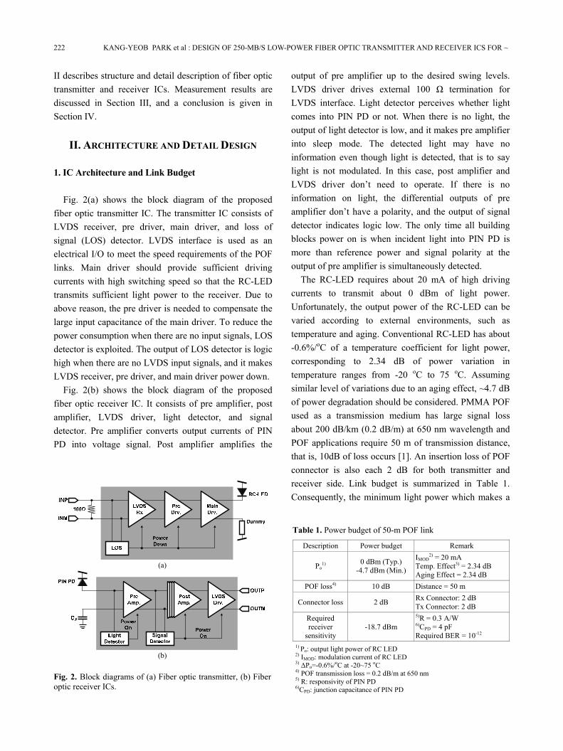
1. IC Architecture and Link Budget Fig. 2(a) shows the block diagram of the proposed
fiber optic transmitter IC. The transmitter IC consists of LVDS receiver, pre driver, main driver, and loss of signal (LOS) detector. LVDS interface is used as an electrical I/O to meet the speed requirements of the POF links. Main driver should provide sufficient driving currents with high switching speed so that the RC-LED transmits sufficient light power to the receiver. Due to above reason, the pre driver is needed to compensate the large input capacitance of the main driver. To reduce the power consumption when there are no input signals, LOS detector is exploited. The output of LOS detector is logic high when there are no LVDS input signals, and it makes LVDS receiver, pre driver, and main driver power down.
Fig. 2(b) shows the block diagram of the proposed fiber optic receiver IC. It consists of pre amplifier, post amplifier, LVDS driver, light detector, and signal detector. Pre amplifier converts output currents of PIN PD into voltage signal. Post amplifier amplifies the
output of pre amplifier up to the desired swing levels. LVDS driver drives external 100 Ω termination for LVDS interface. Light detector perceives whether light comes into PIN PD or not. When there is no light, the output of light detector is low, and it makes pre amplifier into sleep mode. The detected light may have no information even though light is detected, that is to say light is not modulated. In this case, post amplifier and LVDS driver don’t need to operate. If there is no information on light, the differential outputs of pre amplifier don’t have a polarity, and the output of signal detector indicates logic low. The only time all building blocks power on is when incident light into PIN PD is more than reference power and signal polarity at the output of pre amplifier is simultaneously detected.
The RC-LED requires about 20 mA of high driving currents to transmit about 0 dBm of light power. Unfortunately, the output power of the RC-LED can be varied according to external environments, such as temperature and aging. Conventional RC-LED has about -0.6%/oC of a temperature coefficient for light power, corresponding to 2.34 dB of power variation in temperature ranges from -20 oC to 75 oC. Assuming similar level of variations due to an aging effect, ~4.7 dB of power degradation should be considered. PMMA POF used as a transmission medium has large signal loss about 200 dB/km (0.2 dB/m) at 650 nm wavelength and POF applications require 50 m of transmission distance, that is, 10dB of loss occurs [1]. An insertion loss of POF connector is also each 2 dB for both transmitter and receiver side. Link budget is summarized in Table 1. Consequently, the minimum light power which makes a
(a)
(b)
Fig. 2. Block diagrams of (a) Fiber optic transmitter, (b) Fiber optic receiver ICs.
Table 1. Power budget of 50-m POF link
Description Power budget Remark
Po1) 0 dBm (Typ.)
-4.7 dBm (Min.)
IMOD2) = 20 mA
Temp. Effect3) = 2.34 dB Aging Effect = 2.34 dB
POF loss4) 10 dB Distance = 50 m
Connector loss 2 dB Rx Connector: 2 dB Tx Connector: 2 dB
Required receiver
sensitivity -18.7 dBm
5)R = 0.3 A/W 6)CPD = 4 pF Required BER = 10-12
1) Po: output light power of RC LED 2) IMOD: modulation current of RC LED 3) ΔPo=-0.6%/oC at -20~75 oC 4) POF transmission loss = 0.2 dB/m at 650 nm 5) R: responsivity of PIN PD 6)CPD: junction capacitance of PIN PD
JOURNAL OF SEMICONDUCTOR TECHNOLOGY AND SCIENCE, VOL.11, NO.3, SEPTEMBER, 2011 223
bit error rate (BER) of receiver IC be less than 10-12 for 250-Mb/s non-return-to-zero (NRZ) data, i.e. receiver sensitivity, is -18.7 dBm with PIN PD having 0.3 A/W of responsivity and 4pF of junction capacitance (CPD). To provide robustness against uncertainty of the POF link and the ICs, the target sensitivity of the receiver is determined -21.6 dBm.
2. Transmitter Design Details
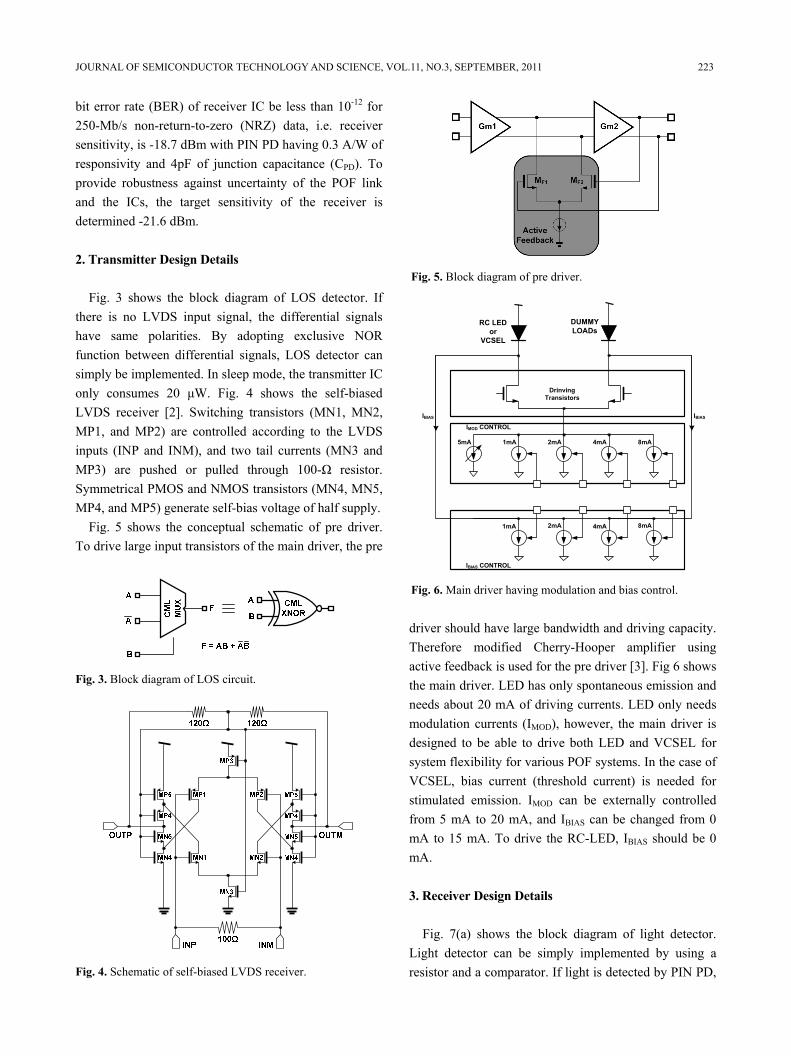
Fig. 3 shows the block diagram of LOS detector. If
there is no LVDS input signal, the differential signals have same polarities. By adopting exclusive NOR function between differential signals, LOS detector can simply be implemented. In sleep mode, the transmitter IC only consumes 20 μW. Fig. 4 shows the self-biased LVDS receiver [2]. Switching transistors (MN1, MN2, MP1, and MP2) are controlled according to the LVDS inputs (INP and INM), and two tail currents (MN3 and MP3) are pushed or pulled through 100-Ω resistor. Symmetrical PMOS and NMOS transistors (MN4, MN5, MP4, and MP5) generate self-bias voltage of half supply.
Fig. 5 shows the conceptual schematic of pre driver. To drive large input transistors of the main driver, the pre
driver should have large bandwidth and driving capacity. Therefore modified Cherry-Hooper amplifier using active feedback is used for the pre driver [3]. Fig 6 shows the main driver. LED has only spontaneous emission and needs about 20 mA of driving currents. LED only needs modulation currents (IMOD), however, the main driver is designed to be able to drive both LED and VCSEL for system flexibility for various POF systems. In the case of VCSEL, bias current (threshold current) is needed for stimulated emission. IMOD can be externally controlled from 5 mA to 20 mA, and IBIAS can be changed from 0 mA to 15 mA. To drive the RC-LED, IBIAS should be 0 mA.
3. Receiver Design Details
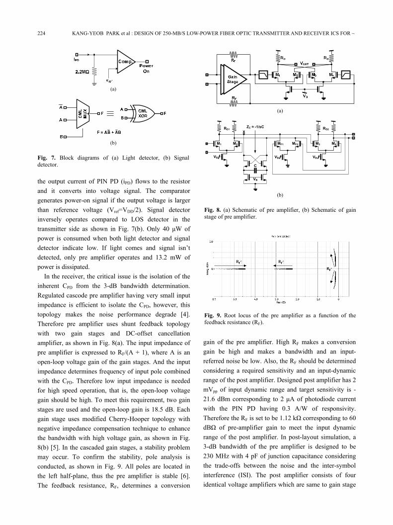
Fig. 7(a) shows the block diagram of light detector.
Light detector can be simply implemented by using a resistor and a comparator. If light is detected by PIN PD,
Fig. 3. Block diagram of LOS circuit.
Fig. 4. Schematic of self-biased LVDS receiver.
Fig. 5. Block diagram of pre driver.
RC LEDor
VCSEL
DUMMYLOADs
5mA 1mA 2mA 4mA 8mA
IMOD CONTROL
DrinvingTransistors
1mA 2mA 4mA 8mA
IBIAS CONTROL
IBIAS IBIAS
Fig. 6. Main driver having modulation and bias control.
224 KANG-YEOB PARK et al : DESIGN OF 250-MB/S LOW-POWER FIBER OPTIC TRANSMITTER AND RECEIVER ICS FOR ~
the output current of PIN PD (iPD) flows to the resistor and it converts into voltage signal. The comparator generates power-on signal if the output voltage is larger than reference voltage (Vref=VDD/2). Signal detector inversely operates compared to LOS detector in the transmitter side as shown in Fig. 7(b). Only 40 μW of power is consumed when both light detector and signal detector indicate low. If light comes and signal isn’t detected, only pre amplifier operates and 13.2 mW of power is dissipated.
In the receiver, the critical issue is the isolation of the inherent CPD from the 3-dB bandwidth determination. Regulated cascode pre amplifier having very small input impedance is efficient to isolate the CPD, however, this topology makes the noise performance degrade [4]. Therefore pre amplifier uses shunt feedback topology with two gain stages and DC-offset cancellation amplifier, as shown in Fig. 8(a). The input impedance of pre amplifier is expressed to RF/(A + 1), where A is an open-loop voltage gain of the gain stages. And the input impedance determines frequency of input pole combined with the CPD. Therefore low input impedance is needed for high speed operation, that is, the open-loop voltage gain should be high. To meet this requirement, two gain stages are used and the open-loop gain is 18.5 dB. Each gain stage uses modified Cherry-Hooper topology with negative impedance compensation technique to enhance the bandwidth with high voltage gain, as shown in Fig. 8(b) [5]. In the cascaded gain stages, a stability problem may occur. To confirm the stability, pole analysis is conducted, as shown in Fig. 9. All poles are located in the left half-plane, thus the pre amplifier is stable [6]. The feedback resistance, RF, determines a conversion
gain of the pre amplifier. High RF makes a conversion gain be high and makes a bandwidth and an input-referred noise be low. Also, the RF should be determined considering a required sensitivity and an input-dynamic range of the post amplifier. Designed post amplifier has 2 mVpp of input dynamic range and target sensitivity is -21.6 dBm corresponding to 2 μA of photodiode current with the PIN PD having 0.3 A/W of responsivity. Therefore the RF is set to be 1.12 kΩ corresponding to 60 dBΩ of pre-amplifier gain to meet the input dynamic range of the post amplifier. In post-layout simulation, a 3-dB bandwidth of the pre amplifier is designed to be 230 MHz with 4 pF of junction capacitance considering the trade-offs between the noise and the inter-symbol interference (ISI). The post amplifier consists of four identical voltage amplifiers which are same to gain stage
(a)
(b)
Fig. 7. Block diagrams of (a) Light detector, (b) Signal detector.
(a)
VB
VB
M1 M2
C
VB VB
M3 M4MF1 MF2
RD1 RD2X
ZC ≈ -1/sC
(b)
Fig. 8. (a) Schematic of pre amplifier, (b) Schematic of gain stage of pre amplifier.
Fig. 9. Root locus of the pre amplifier as a function of the feedback resistance (RF).
JOURNAL OF SEMICONDUCTOR TECHNOLOGY AND SCIENCE, VOL.11, NO.3, SEPTEMBER, 2011 225
of pre amplifier. For differential 400-mVpp fixed output swing against -21.6 dBm of light power, total conversion gain should be above 105 dBΩ. Therefore the post amplifier exhibit 45 dB of voltage gain and 320 MHz of 3-dB bandwidth in the post-layout simulation. The LVDS driver uses conventional differential common-source pair to drive 100-Ω off-chip resistor and acts as an output buffer. The receiver chip only consumes 52.8 mW from a 3.3 V single supply.
III. MEASUREMENT RESULTS
1. Chip Implementation The 250-Mb/s fiber optic transmitter and receiver ICs
for plastic optical fiber applications are implemented using a CMOS technology. Fig. 10 shows the chip photographs of the fiber optic transmitter and receiver ICs. Each IC occupies 0.85 mm × 0.73 mm of area including electrostatic discharge (ESD) protection diodes
pads which can endure up to 2 kV. Total transmitter and receiver ICs consume 75.9 mW with 20-mA LED driving currents and 52.8 mW with 4-mA output driving currents at a single 3.3 V supply, respectively. Fig. 11 shows the microphotographs of the assembled ICs with optical devices on TOCAN-type package. They are connected by boding wire for prototype test.
2. Measurement Setup and Results
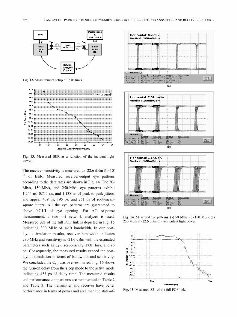
Fig. 12 shows the measurement setup. The packaged
ICs and optical devices are integrated with passive elements on a printed-circuit-board. The PIN PD operates at 650 nm of center wavelength and exhibits 250 MHz of 3-dB bandwidth, 0.3 A/W of responsivity, and 4 pF of CPD.
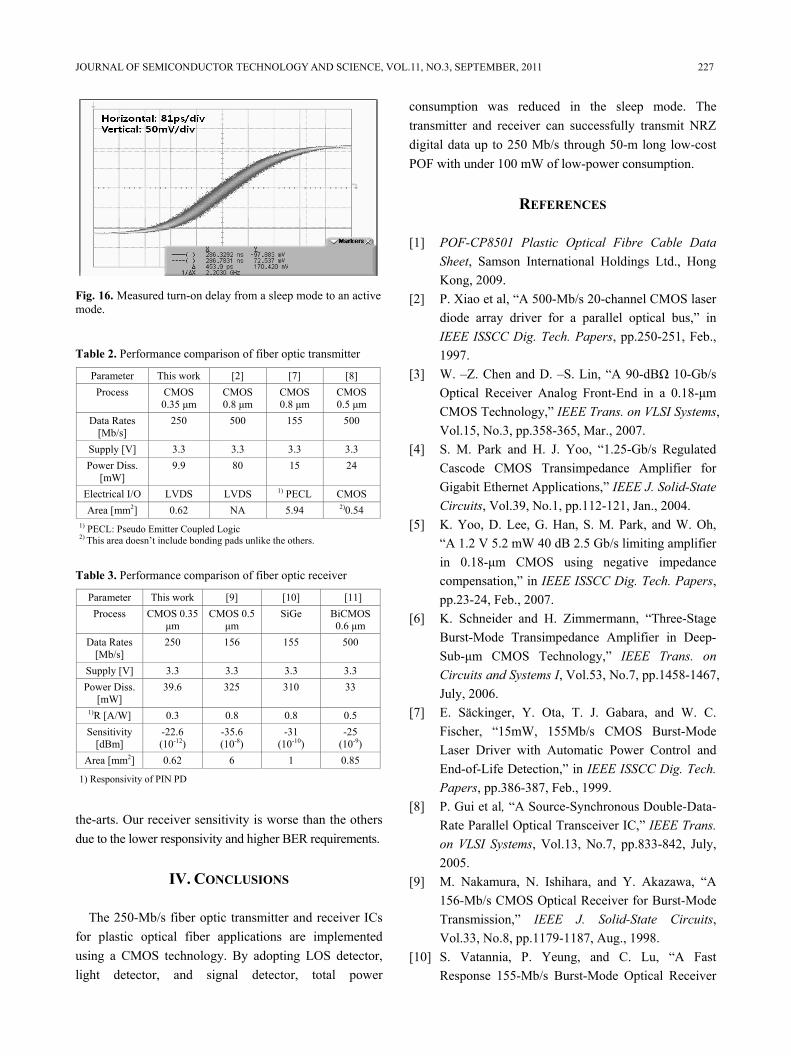
A pulse pattern generator (PPG) creates PRBS 231-1 NRZ data for measurements. This data is converted into light data by the fiber optic transmitter. This 650 nm light signal is transmitted through 50-m PMMA POF. An optical attenuator is used for the receiver sensitivity measurement. Measured BER through full POF link as a function of the received light power is depicted in Fig. 13.
(a)
(b)
Fig. 10. Chip microphotographs of (a) Fiber optic transmitter,(b) Fiber optic receiver ICs.
(a)
(b)
Fig. 11. Assembled FOT modules. (a) Fiber optic transmitter IC with RC-LED, (b) Fiber optic receiver IC with PIN PD.
226 KANG-YEOB PARK et al : DESIGN OF 250-MB/S LOW-POWER FIBER OPTIC TRANSMITTER AND RECEIVER ICS FOR ~
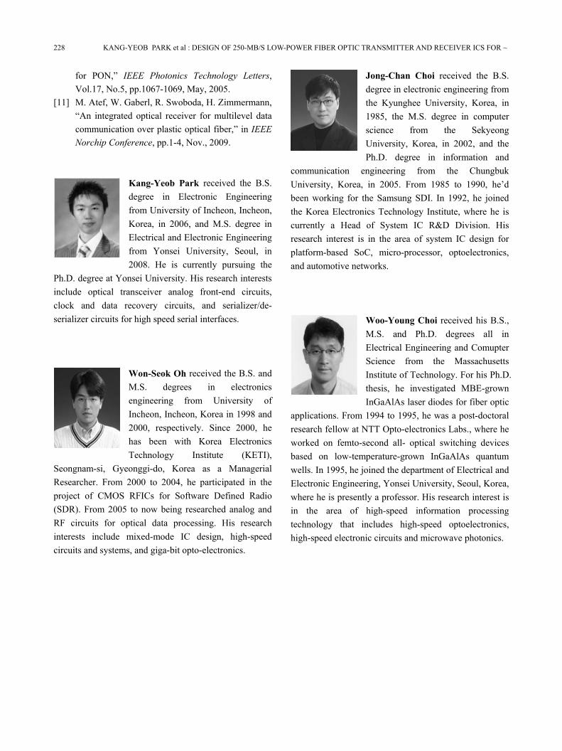
The receiver sensitivity is measured to -22.6 dBm for 10-
12 of BER. Measured receiver-output eye patterns according to the data rates are shown in Fig. 14. The 50-Mb/s, 150-Mb/s, and 250-Mb/s eye patterns exhibit 1.244 ns, 0.711 ns, and 1.138 ns of peak-to-peak jitters, and appear 439 ps, 195 ps, and 251 ps of root-mean-square jitters. All the eye patterns are guaranteed to above 0.7-UI of eye opening. For AC response measurement, a two-port network analyzer is used. Measured S21 of the full POF link is depicted in Fig. 15 indicating 300 MHz of 3-dB bandwidth. In our post-layout simulation results, receiver bandwidth indicates 230 MHz and sensitivity is -21.6 dBm with the estimated parameters such as CPD, responsivity, POF loss, and so on. Consequently, the measured results exceed the post-layout simulation in terms of bandwidth and sensitivity. We concluded the CPD was over-estimated. Fig. 16 shows the turn-on delay from the sleep mode to the active mode indicating 453 ps of delay time. The measured results and performance comparisons are summarized in Table 2 and Table 3. The transmitter and receiver have better performance in terms of power and area than the state-of-
(a)
(b)
(c)
Fig. 14. Measured eye patterns. (a) 50 Mb/s, (b) 150 Mb/s, (c) 250 Mb/s at -22.6 dBm of the incident light power.
Fig. 15. Measured S21 of the full POF link.
Fig. 12. Measurement setup of POF links.
Fig. 13. Measured BER as a function of the incident light power.
JOURNAL OF SEMICONDUCTOR TECHNOLOGY AND SCIENCE, VOL.11, NO.3, SEPTEMBER, 2011 227
the-arts. Our receiver sensitivity is worse than the others due to the lower responsivity and higher BER requirements.
IV. CONCLUSIONS
The 250-Mb/s fiber optic transmitter and receiver ICs for plastic optical fiber applications are implemented using a CMOS technology. By adopting LOS detector, light detector, and signal detector, total power
consumption was reduced in the sleep mode. The transmitter and receiver can successfully transmit NRZ digital data up to 250 Mb/s through 50-m long low-cost POF with under 100 mW of low-power consumption.
REFERENCES
[1] POF-CP8501 Plastic Optical Fibre Cable Data Sheet, Samson International Holdings Ltd., Hong Kong, 2009.
[2] P. Xiao et al, “A 500-Mb/s 20-channel CMOS laser diode array driver for a parallel optical bus,” in IEEE ISSCC Dig. Tech. Papers, pp.250-251, Feb., 1997.
[3] W. –Z. Chen and D. –S. Lin, “A 90-dBΩ 10-Gb/s Optical Receiver Analog Front-End in a 0.18-μm CMOS Technology,” IEEE Trans. on VLSI Systems, Vol.15, No.3, pp.358-365, Mar., 2007.
[4] S. M. Park and H. J. Yoo, “1.25-Gb/s Regulated Cascode CMOS Transimpedance Amplifier for Gigabit Ethernet Applications,” IEEE J. Solid-State Circuits, Vol.39, No.1, pp.112-121, Jan., 2004.
[5] K. Yoo, D. Lee, G. Han, S. M. Park, and W. Oh, “A 1.2 V 5.2 mW 40 dB 2.5 Gb/s limiting amplifier in 0.18-μm CMOS using negative impedance compensation,” in IEEE ISSCC Dig. Tech. Papers, pp.23-24, Feb., 2007.
[6] K. Schneider and H. Zimmermann, “Three-Stage Burst-Mode Transimpedance Amplifier in Deep-Sub-μm CMOS Technology,” IEEE Trans. on Circuits and Systems I, Vol.53, No.7, pp.1458-1467, July, 2006.
[7] E. Säckinger, Y. Ota, T. J. Gabara, and W. C. Fischer, “15mW, 155Mb/s CMOS Burst-Mode Laser Driver with Automatic Power Control and End-of-Life Detection,” in IEEE ISSCC Dig. Tech. Papers, pp.386-387, Feb., 1999.
[8] P. Gui et al, “A Source-Synchronous Double-Data-Rate Parallel Optical Transceiver IC,” IEEE Trans. on VLSI Systems, Vol.13, No.7, pp.833-842, July, 2005.
[9] M. Nakamura, N. Ishihara, and Y. Akazawa, “A 156-Mb/s CMOS Optical Receiver for Burst-Mode Transmission,” IEEE J. Solid-State Circuits, Vol.33, No.8, pp.1179-1187, Aug., 1998.
[10] S. Vatannia, P. Yeung, and C. Lu, “A Fast Response 155-Mb/s Burst-Mode Optical Receiver
Fig. 16. Measured turn-on delay from a sleep mode to an active mode.
Table 2. Performance comparison of fiber optic transmitter
Parameter This work [2] [7] [8] Process CMOS
0.35 μm CMOS 0.8 μm
CMOS 0.8 μm
CMOS 0.5 μm
Data Rates [Mb/s]
250 500 155 500
Supply [V] 3.3 3.3 3.3 3.3 Power Diss.
[mW] 9.9 80 15 24
Electrical I/O LVDS LVDS 1) PECL CMOS Area [mm2] 0.62 NA 5.94 2)0.54
1) PECL: Pseudo Emitter Coupled Logic 2) This area doesn’t include bonding pads unlike the others.
Table 3. Performance comparison of fiber optic receiver
Parameter This work [9] [10] [11] Process CMOS 0.35
μm CMOS 0.5
μm SiGe BiCMOS
0.6 μm Data Rates
[Mb/s] 250 156 155 500
Supply [V] 3.3 3.3 3.3 3.3 Power Diss.
[mW] 39.6 325 310 33
1)R [A/W] 0.3 0.8 0.8 0.5 Sensitivity
[dBm] -22.6 (10-12)
-35.6 (10-8)
-31 (10-10)
-25 (10-9)
Area [mm2] 0.62 6 1 0.85
1) Responsivity of PIN PD
228 KANG-YEOB PARK et al : DESIGN OF 250-MB/S LOW-POWER FIBER OPTIC TRANSMITTER AND RECEIVER ICS FOR ~
for PON,” IEEE Photonics Technology Letters, Vol.17, No.5, pp.1067-1069, May, 2005.
[11] M. Atef, W. Gaberl, R. Swoboda, H. Zimmermann, “An integrated optical receiver for multilevel data communication over plastic optical fiber,” in IEEE Norchip Conference, pp.1-4, Nov., 2009.
Kang-Yeob Park received the B.S. degree in Electronic Engineering from University of Incheon, Incheon, Korea, in 2006, and M.S. degree in Electrical and Electronic Engineering from Yonsei University, Seoul, in 2008. He is currently pursuing the
Ph.D. degree at Yonsei University. His research interests include optical transceiver analog front-end circuits, clock and data recovery circuits, and serializer/de-serializer circuits for high speed serial interfaces.
Won-Seok Oh received the B.S. and M.S. degrees in electronics engineering from University of Incheon, Incheon, Korea in 1998 and 2000, respectively. Since 2000, he has been with Korea Electronics Technology Institute (KETI),
Seongnam-si, Gyeonggi-do, Korea as a Managerial Researcher. From 2000 to 2004, he participated in the project of CMOS RFICs for Software Defined Radio (SDR). From 2005 to now being researched analog and RF circuits for optical data processing. His research interests include mixed-mode IC design, high-speed circuits and systems, and giga-bit opto-electronics.
Jong-Chan Choi received the B.S. degree in electronic engineering from the Kyunghee University, Korea, in 1985, the M.S. degree in computer science from the Sekyeong University, Korea, in 2002, and the Ph.D. degree in information and
communication engineering from the Chungbuk University, Korea, in 2005. From 1985 to 1990, he’d been working for the Samsung SDI. In 1992, he joined the Korea Electronics Technology Institute, where he is currently a Head of System IC R&D Division. His research interest is in the area of system IC design for platform-based SoC, micro-processor, optoelectronics, and automotive networks.
Woo-Young Choi received his B.S., M.S. and Ph.D. degrees all in Electrical Engineering and Comupter Science from the Massachusetts Institute of Technology. For his Ph.D. thesis, he investigated MBE-grown InGaAlAs laser diodes for fiber optic
applications. From 1994 to 1995, he was a post-doctoral research fellow at NTT Opto-electronics Labs., where he worked on femto-second all- optical switching devices based on low-temperature-grown InGaAlAs quantum wells. In 1995, he joined the department of Electrical and Electronic Engineering, Yonsei University, Seoul, Korea, where he is presently a professor. His research interest is in the area of high-speed information processing technology that includes high-speed optoelectronics, high-speed electronic circuits and microwave photonics.