Embed Size (px)
Citation preview
Design Methodology Based on Carbon Nanotube Field
Effect Transistor(CNFET)
A Thesis Presented
by
Young Bok Kim
to
The Department of Department of Electrical and Computer Engineering
in partial fulfillment of the requirements
for the degree of
Doctor of Philosophy
in
Electrical Engineering
in the field of
Computer Engineering
Northeastern University
Boston, Massachusetts
January 2011

c⃝ Copyright 2011 by Young Bok Kim
All Rights Reserved
NORTHEASTERN UNIVERSITYGraduate School of Engineering
Thesis Title: Design Methodology Based on Carbon Nanotube Field Effect
Transistor(CNFET) .
Author: Young Bok Kim.
Department: Department of Electrical and Computer Engineering.
Approved for Thesis Requirements of the Doctor of Philosophy Degree
Thesis Advisor: Prof. Yong-Bin Kim Date
Thesis Reader: Prof. Fabrizio Lombardi Date
Thesis Reader: Prof. Nian Sun Date
Department Chair: Prof. Ali Abur Date
Graduate School Notified of Acceptance:
Director of the Graduate School Date
NORTHEASTERN UNIVERSITYGraduate School of Engineering
Thesis Title: Design Methodology Based on Carbon Nanotube Field Effect
Transistor(CNFET) .
Author: Young Bok Kim.
Department: Department of Electrical and Computer Engineering.
Approved for Thesis Requirements of the Doctor of Philosophy Degree
Thesis Advisor: Prof. Yong-Bin Kim Date
Thesis Reader: Prof. Fabrizio Lombardi Date
Thesis Reader: Prof. Nian Sun Date
Department Chair: Prof. Ali Abur Date
Graduate School Notified of Acceptance:
Dean: Prof. Date
Copy Deposited in Library:
Reference Librarian Date
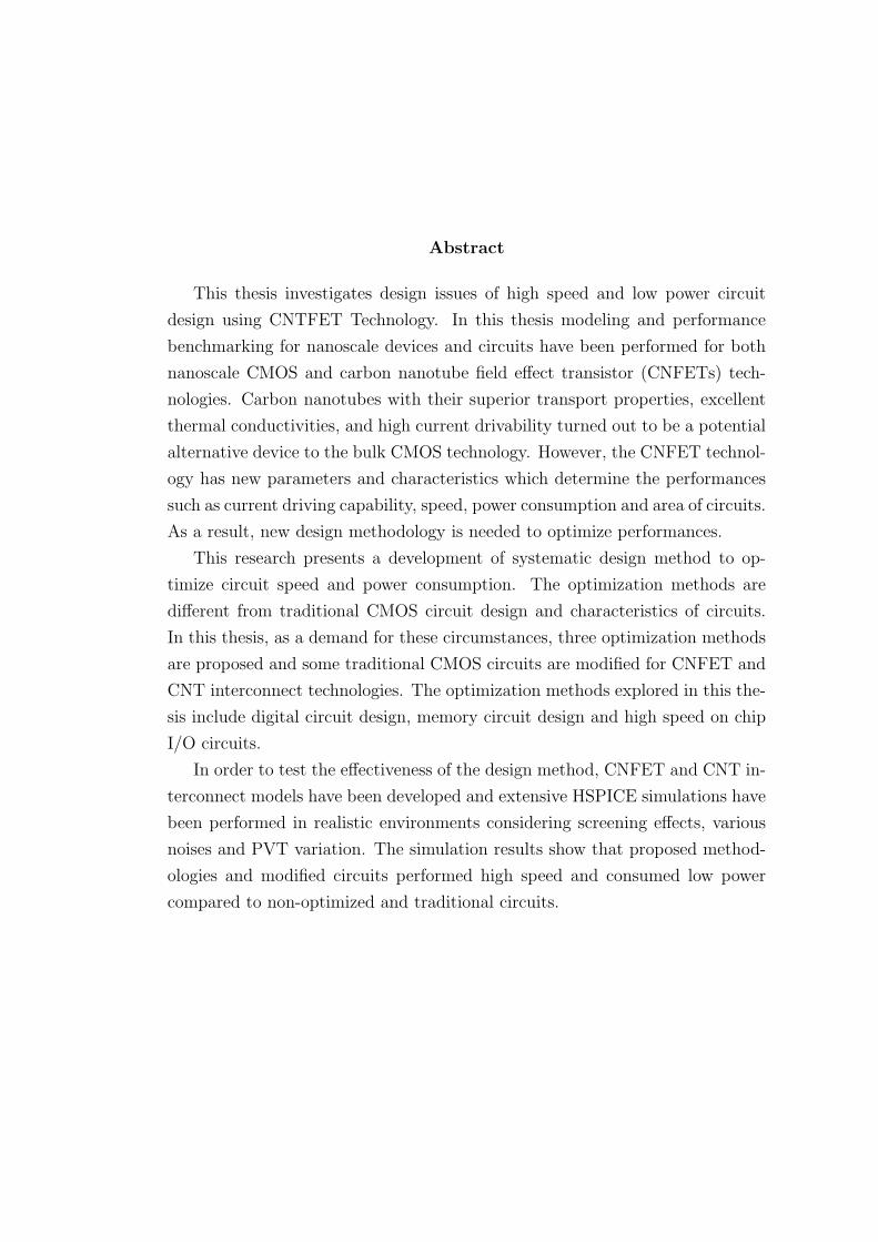
Abstract
This thesis investigates design issues of high speed and low power circuit
design using CNTFET Technology. In this thesis modeling and performance
benchmarking for nanoscale devices and circuits have been performed for both
nanoscale CMOS and carbon nanotube field effect transistor (CNFETs) tech-
nologies. Carbon nanotubes with their superior transport properties, excellent
thermal conductivities, and high current drivability turned out to be a potential
alternative device to the bulk CMOS technology. However, the CNFET technol-
ogy has new parameters and characteristics which determine the performances
such as current driving capability, speed, power consumption and area of circuits.
As a result, new design methodology is needed to optimize performances.
This research presents a development of systematic design method to op-
timize circuit speed and power consumption. The optimization methods are
different from traditional CMOS circuit design and characteristics of circuits.
In this thesis, as a demand for these circumstances, three optimization methods
are proposed and some traditional CMOS circuits are modified for CNFET and
CNT interconnect technologies. The optimization methods explored in this the-
sis include digital circuit design, memory circuit design and high speed on chip
I/O circuits.
In order to test the effectiveness of the design method, CNFET and CNT in-
terconnect models have been developed and extensive HSPICE simulations have
been performed in realistic environments considering screening effects, various
noises and PVT variation. The simulation results show that proposed method-
ologies and modified circuits performed high speed and consumed low power
compared to non-optimized and traditional circuits.

Acknowledgements
First of all, I must thank Dr. Yong-Bin Kim, my academic and research
advisor, not only for his invaluable advice and encouragement leading me in
the process of fulfilling my master research, but also for his great guidance and
help during my four year PhD study. I would also like to thank the members of
committee.
Young Bok Kim
Boston,MA

For my parents
Contents
Acknowledgements i
1 Introduction 1
1.1 Nanoscale MOSFET . . . . . . . . . . . . . . . . . . . . . . . . 3
1.2 Carbon Nanotube Field-Effect Transistors . . . . . . . . . . . . 4
1.2.1 Carbon nanotube . . . . . . . . . . . . . . . . . . . . . . 4
1.2.2 CNFET . . . . . . . . . . . . . . . . . . . . . . . . . . . 6
1.3 Thesis Outline . . . . . . . . . . . . . . . . . . . . . . . . . . . . 7
2 Analysis of CNFET Technology 10
2.1 CNFET Technology . . . . . . . . . . . . . . . . . . . . . . . . . 10
2.2 Performance Analysis between CNFET and CMOS Under PVT
Variation . . . . . . . . . . . . . . . . . . . . . . . . . . . . . . . 12
2.2.1 Deciciding ratio between PMOS and NMOS . . . . . . . 13
2.2.2 Logic gates performance analysis . . . . . . . . . . . . . 14
2.2.3 Logic gates PVT variations . . . . . . . . . . . . . . . . 17
2.2.4 Performance analysis of benchmark circuits . . . . . . . . 28
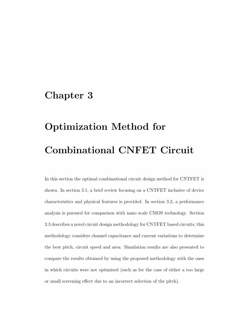
3 Optimization Method for Combinational CNFET Circuit 30
3.1 Analysis of Technology Parameters . . . . . . . . . . . . . . . . 31
3.1.1 Channel and gate capacitance vs pitch . . . . . . . . . . 31
3.1.2 Size of CNFET . . . . . . . . . . . . . . . . . . . . . . . 36
3.1.3 CNFET threshold voltage . . . . . . . . . . . . . . . . . 36
3.2 Performance Opimization Methods . . . . . . . . . . . . . . . . 39
3.2.1 Optimization for CNFET-based circuits . . . . . . . . . 39
3.2.2 Simulations results for combinational circuits . . . . . . . 46
3.3 Summary . . . . . . . . . . . . . . . . . . . . . . . . . . . . . . 53
4 Low Power SRAM Design using CNFET 55
4.1 Introduction . . . . . . . . . . . . . . . . . . . . . . . . . . . . . 55
4.2 Low power 8T SRAM Cell . . . . . . . . . . . . . . . . . . . . . 57
4.2.1 Write/Read operations . . . . . . . . . . . . . . . . . . . 57
4.2.2 Carbon nanotube configuration . . . . . . . . . . . . . . 58
4.3 SIMULATION RESULTS . . . . . . . . . . . . . . . . . . . . . 60
4.3.1 Simulation setup . . . . . . . . . . . . . . . . . . . . . . 61
4.3.2 Dynamic power consumption . . . . . . . . . . . . . . . 62
4.3.3 Leakage power consumption . . . . . . . . . . . . . . . . 63
4.3.4 Cell stability . . . . . . . . . . . . . . . . . . . . . . . . 64
4.4 Summary . . . . . . . . . . . . . . . . . . . . . . . . . . . . . . 66
5 High Speed and Low Power Transceiver Design for CNFET and
CNT Interconnect 68
5.1 Introduction . . . . . . . . . . . . . . . . . . . . . . . . . . . . . 68
5.2 CNT interconnect technologies . . . . . . . . . . . . . . . . . . . 71
5.3 PWAM SCHEME . . . . . . . . . . . . . . . . . . . . . . . . . . 72
5.4 Driving a Wire with a Capacitor . . . . . . . . . . . . . . . . . 74
5.5 Energy Consumption Of Transceiver . . . . . . . . . . . . . . . 75
5.6 4-PWAM Circuit Design . . . . . . . . . . . . . . . . . . . . . . 76
5.6.1 Transmitter circuit . . . . . . . . . . . . . . . . . . . . . 76
5.6.2 Receiver circuits . . . . . . . . . . . . . . . . . . . . . . . 79
5.7 Noise models and Bit Error Rate . . . . . . . . . . . . . . . . . 82
5.7.1 Noise models . . . . . . . . . . . . . . . . . . . . . . . . 82
5.7.2 Bit error rate (BER) estimation . . . . . . . . . . . . . . 83
5.8 Simulation Results . . . . . . . . . . . . . . . . . . . . . . . . . 85
5.8.1 Simulation setup . . . . . . . . . . . . . . . . . . . . . . 85
5.8.2 Eye diagram analysis . . . . . . . . . . . . . . . . . . . . 86
5.9 Summary . . . . . . . . . . . . . . . . . . . . . . . . . . . . . . 93
6 Conclusion 94
6.1 Conclusion . . . . . . . . . . . . . . . . . . . . . . . . . . . . . . 94

Bibliography 98

List of Tables
2.1 Delay, Power, and PDP for 32nm MOSFET and 32nm CNFET
logic gates. . . . . . . . . . . . . . . . . . . . . . . . . . . . . . . 17
2.2 Delay, Power, and PDP for 32nm MOSFET and CNFET circuits. 29
3.1 η versus pitch (VDD = 0.6V, diameter = 2nm, channel length =
32nm). . . . . . . . . . . . . . . . . . . . . . . . . . . . . . . . . 35
3.2 Delay, Power and PDP of the FO4 inverter for various Vth. . . 38
3.3 γ Values for 4nm, 10nm pitches with different number of tubes. 43
3.4 Logical Effort for CNTFET. . . . . . . . . . . . . . . . . . . . . 44
3.5 Logical Effort for 32nm CMOS. . . . . . . . . . . . . . . . . . . 45
3.6 Delay, Power and PDP for 32nm MOSFET and CNTFET circuits. 53
5.1 Decoded bit2, bit 3 from comparator out. . . . . . . . . . . . . . 82
5.2 Bit Error rate with Random jitter and PVT variation. . . . . . 92
5.3 Summary of the performances and comparison. . . . . . . . . . 92
List of Figures
1.1 The physical gate length and the contacted gate pitch of the fab-
ricated devices and projected by ITRS[1]. . . . . . . . . . . . . . 2
1.2 Unrolled graphite sheet and the rolled carbon nanotube lattice
structure. . . . . . . . . . . . . . . . . . . . . . . . . . . . . . . 4
1.3 The energy band diagram for (a) SB-CNFET and (b) MOSFET-
like CNFET. . . . . . . . . . . . . . . . . . . . . . . . . . . . . . 7
2.1 CNFET Structure. . . . . . . . . . . . . . . . . . . . . . . . . . 11
2.2 Voltage Transfer Characteristic (VTC) for 32nm MOSFET and
CNFET inverters at 0.9V supply. . . . . . . . . . . . . . . . . . 15
2.3 Voltage Transfer Characteristic (VTC) of 32nm CNFET andMOS-
FET inverters at different power supplies. . . . . . . . . . . . . 15
2.4 Maximum and minimum leakage power for 32nm MOSFET and
CNFET logic gates. . . . . . . . . . . . . . . . . . . . . . . . . . 19
2.5 Frequency response for 32nm MOSFET and CNFET inverters. . 20
2.6 IDS vs. VGS curve with 10% change of gate length and width for
the 32nm MOSFET and CNFET. . . . . . . . . . . . . . . . . . 21
2.7 IDS vs. VGS with 10% change of carbon nanotube diameter (chi-
rality) for the 32nm CNFET. . . . . . . . . . . . . . . . . . . . 22
2.8 Power delay product (PDP) of 32nm CNFET logic gates vs. di-
ameter (chirality) of carbon nanotube. . . . . . . . . . . . . . . 22
2.9 Maximum leakage power of the 32nm CNFET logic gates vs. di-
ameter (chirality) of carbon nanotube. . . . . . . . . . . . . . . 23
2.10 Power delay product (PDP) of 32nm MOSFET logic gates vs.
supply voltage. . . . . . . . . . . . . . . . . . . . . . . . . . . . 24
2.11 Power delay product (PDP) of 32nm CNFET logic gates vs. sup-
ply voltage. . . . . . . . . . . . . . . . . . . . . . . . . . . . . . 25
2.12 Maximum leakage power of 32nm MOSFET logic gates vs. supply
voltage. . . . . . . . . . . . . . . . . . . . . . . . . . . . . . . . 25
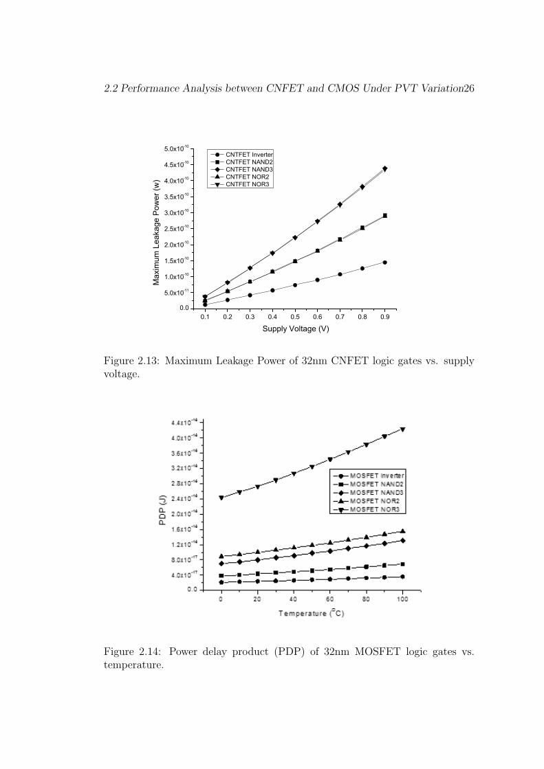
2.13 Maximum Leakage Power of 32nm CNFET logic gates vs. supply
voltage. . . . . . . . . . . . . . . . . . . . . . . . . . . . . . . . 26
2.14 Power delay product (PDP) of 32nm MOSFET logic gates vs.
temperature. . . . . . . . . . . . . . . . . . . . . . . . . . . . . . 26
2.15 Power delay product (PDP) of 32nm CNFET logic gates versus
temperature. . . . . . . . . . . . . . . . . . . . . . . . . . . . . . 27
2.16 Maximum Leakage Power of 32nm MOSFET logic gates vs. tem-
perature. . . . . . . . . . . . . . . . . . . . . . . . . . . . . . . . 27
2.17 Maximum Leakage Power of 32nm CNFET logic gates vs. tem-
perature. . . . . . . . . . . . . . . . . . . . . . . . . . . . . . . . 28
3.1 The CNTs in array and electrode. . . . . . . . . . . . . . . . . . 32
3.2 Three CNTs in parallel to the gate. . . . . . . . . . . . . . . . . 33
3.3 The toal potential due to the adjacent CNT and its image charge. 34
3.4 The gate to middle and edge CNT channel capacitances. . . . . 34
3.5 Drain current with different values of pitch and number of tubes. 37
3.6 Optimization flow overview with given technology parameters. . 39
3.7 Example circuit for optimization method. . . . . . . . . . . . . . 45
3.8 Delay of inverter (channel length =32nm, VDD = 0.6, Vth = 0.2
number of tubes =4) for different pitches. . . . . . . . . . . . . . 47
3.9 Inverter chain delay for different fan-factor and pitch. . . . . . . 48
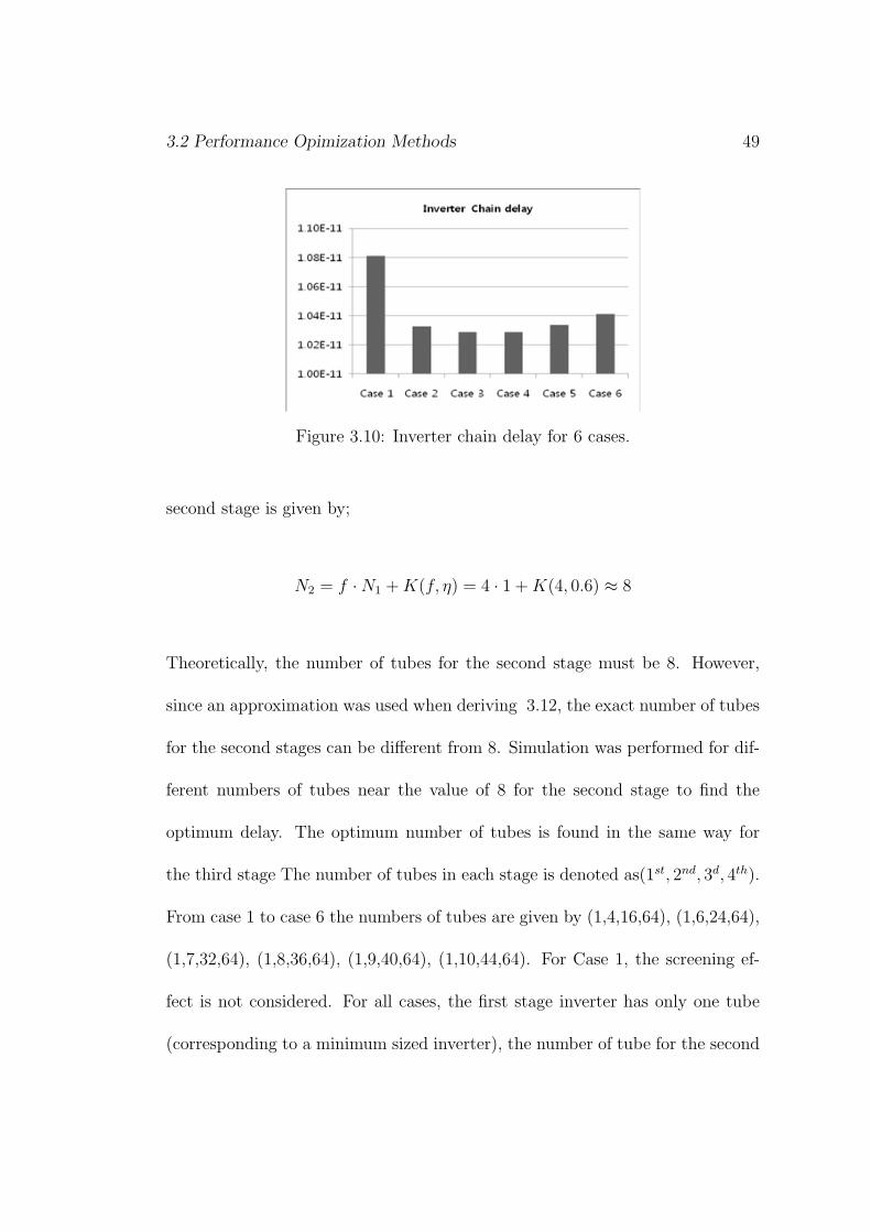
3.10 Inverter chain delay for 6 cases. . . . . . . . . . . . . . . . . . . 49
3.11 Delay of the circuit example for logical effort in Figure 7 (η=0.6
and 4nm pitch, η=1, 20nm pitch for ideal CNTFET case with no
screening effect). . . . . . . . . . . . . . . . . . . . . . . . . . . 51
3.12 Power consumption of inverter (channel length =32nm, VDD =
0.6, Vth = 0.2 number of tubes =4) versus pitch). . . . . . . . . 51
3.13 Power consumption of the test circuit in Figure 23. . . . . . . . 52
4.1 The 8T SRAM CNFET structure. . . . . . . . . . . . . . . . . . 59
4.2 The Dynamic Power consumption with VDD variation . . . . . 63
4.3 The Leakage Power consumption with VDD variation . . . . . 64
4.4 SNM for 6T and 8T CNFET cell with VDD variation . . . . . 65
5.1 CNT bundle interconnect structure. . . . . . . . . . . . . . . . . 71
5.2 The PWAM Signaling (a) Conventional Symbols (b) Conventional
PAM-4 Symbols (c)PWAM-(4× 4) Symbols. . . . . . . . . . . . 73
5.3 The capacitively driven wire ) Symbols. . . . . . . . . . . . . . . 74
5.4 The block diagram of the transmitter. . . . . . . . . . . . . . . 77
5.5 Phase controller. . . . . . . . . . . . . . . . . . . . . . . . . . . 78
5.6 Timing diagram of Phase controller. . . . . . . . . . . . . . . . 78
5.7 Adaptive Capacitance. . . . . . . . . . . . . . . . . . . . . . . . 80
5.8 Receiver circuits. . . . . . . . . . . . . . . . . . . . . . . . . . . 81
5.9 Timing diagram of PWM Demodulation. . . . . . . . . . . . . . 81
5.10 Sum of flicker, thermal, shot noises. . . . . . . . . . . . . . . . . 82
5.11 Wire model for crosstalk noise. . . . . . . . . . . . . . . . . . . 83
5.12 Crosstalk noise caused by large aggressor signal victim signal
without shield technique. . . . . . . . . . . . . . . . . . . . . . . 84
5.13 Crosstalk noise caused by large aggressor signal victim signal with
shield technique. . . . . . . . . . . . . . . . . . . . . . . . . . . 84
5.12 Eye-diagram of received PWAM signals (a) without random jitter,
PVT variations (b) with random jitter (c) with process variation
(d) with process variation and random jitter (e) supply voltage
variation (variation = 0.01) (f) supply voltage variation (variation
= 0.05). . . . . . . . . . . . . . . . . . . . . . . . . . . . . . . . 91
5.13 Receiver circuits. . . . . . . . . . . . . . . . . . . . . . . . . . . 92

Chapter 1
Introduction
Ever since the 0.35µm node, the gate length of MOSFET has entered the deep-
submicron region. 65 nm technology becomes the mainstream since 2006, and 45
nm technology has been announced in 2007. As CMOS continues to scale deeper
into the nanoscale, various device non-idealities cause the I-V characteristics to
be substantially different from well-tempered MOSFETs. It becomes more dif-
ficult to further improve device/circuit performance by reducing the physical
gate length. The discrepancy between the fabricated physical gate length and
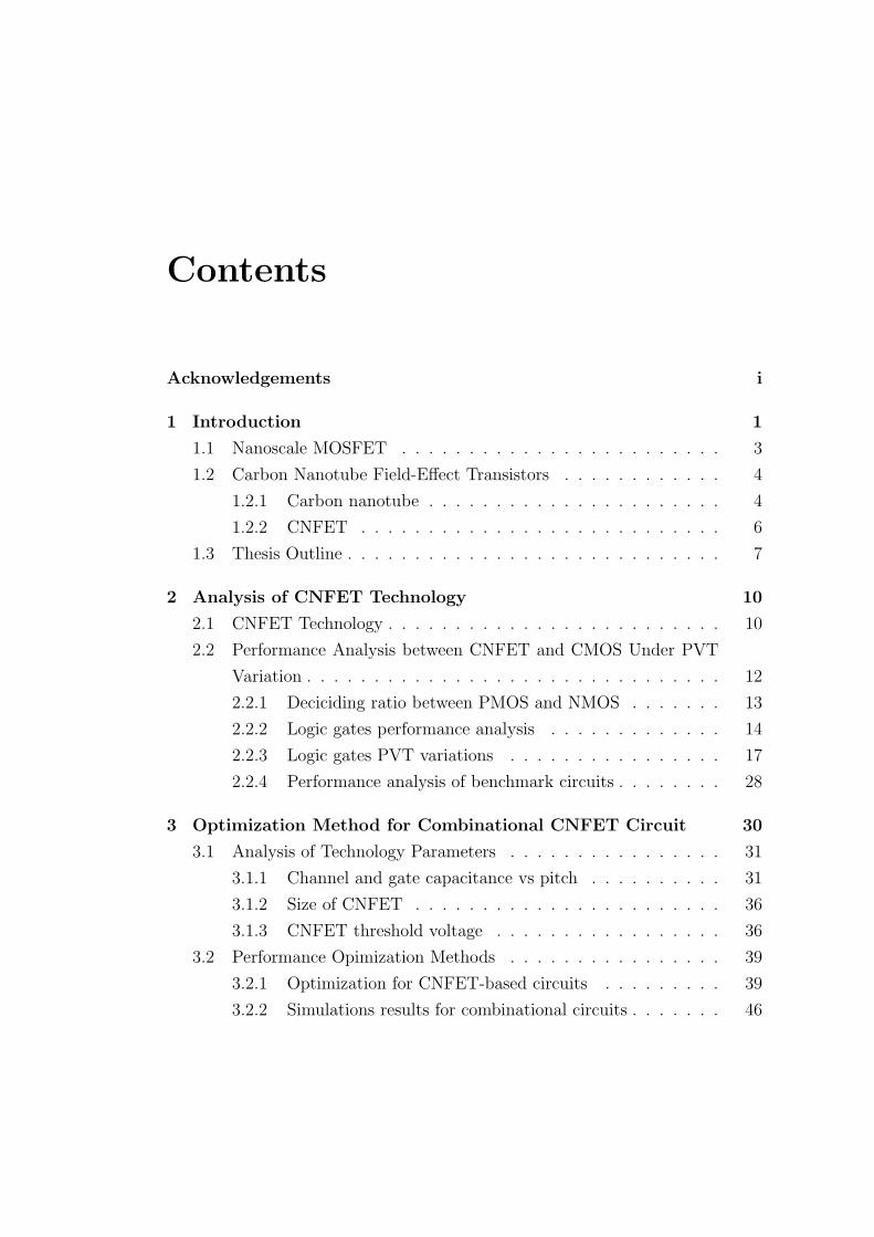
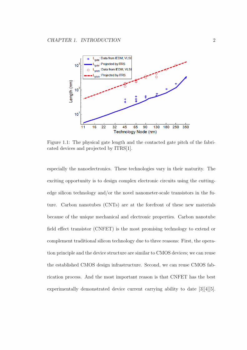
the ITRS [1] projected gate length becomes larger as the technology advances,
as shown in Fig 1.1 . On the other hand, as the major driving force for the
semiconductor industry, the device contacted gate pitch (Lpitch) is scaled down
by a factor of 0.7 every technology node.
The last few years witnessed a dramatic increase in nanotechnology research,
CHAPTER 1. INTRODUCTION 2
Figure 1.1: The physical gate length and the contacted gate pitch of the fabri-cated devices and projected by ITRS[1].
especially the nanoelectronics. These technologies vary in their maturity. The
exciting opportunity is to design complex electronic circuits using the cutting-
edge silicon technology and/or the novel nanometer-scale transistors in the fu-
ture. Carbon nanotubes (CNTs) are at the forefront of these new materials
because of the unique mechanical and electronic properties. Carbon nanotube
field effect transistor (CNFET) is the most promising technology to extend or
complement traditional silicon technology due to three reasons: First, the opera-
tion principle and the device structure are similar to CMOS devices; we can reuse
the established CMOS design infrastructure. Second, we can reuse CMOS fab-
rication process. And the most important reason is that CNFET has the best
experimentally demonstrated device current carrying ability to date [3][4][5].
1.1 Nanoscale MOSFET 3
Technology boosters such as strain have helped the continuation of CMOS his-
toric performance trend up to 45 nm node. As device physical gate length is
reduced to below 25 nm at/beyond 65 nm technology node, various leakage cur-
rents and device parameter variation become the most important considerations
for device optimization. In fact, it can be argued that reduction of gate length
below 25 nm may not offer the same advantage as short-gate devices had pro-
vided historically in terms of power and performance at the system level [8]. The
major detractors are: the lack of a thin equivalent gate oxide (with low leakage
current) for effective short channel effect control, the increasing contribution of
the fringing parasitic capacitance to the total gate capacitance, and the rising
contribution of the source/drain resistance to the total device on-resistance.
1.1 Nanoscale MOSFET
As CMOS continues to scale deeper into the nanoscale, various device non-
idealities cause the I-V characteristics to be substantially different from well-
tempered MOSFETs. For example, the source/drain series resistance is now a
significant component of the total on-resistance. Proposals of metal contacted
(Schottky) source/drain UTB SOI FET [6] also alter the I-V characteristics
significantly. Novel non-Si devices such as the carbon nanotube FETs (CNFETs)
operate with completely different device physics with quasiballistic transport in
the channel [3]and Schottky barriers at the source/drain contacts [7].

1.2 Carbon Nanotube Field-Effect Transistors 4
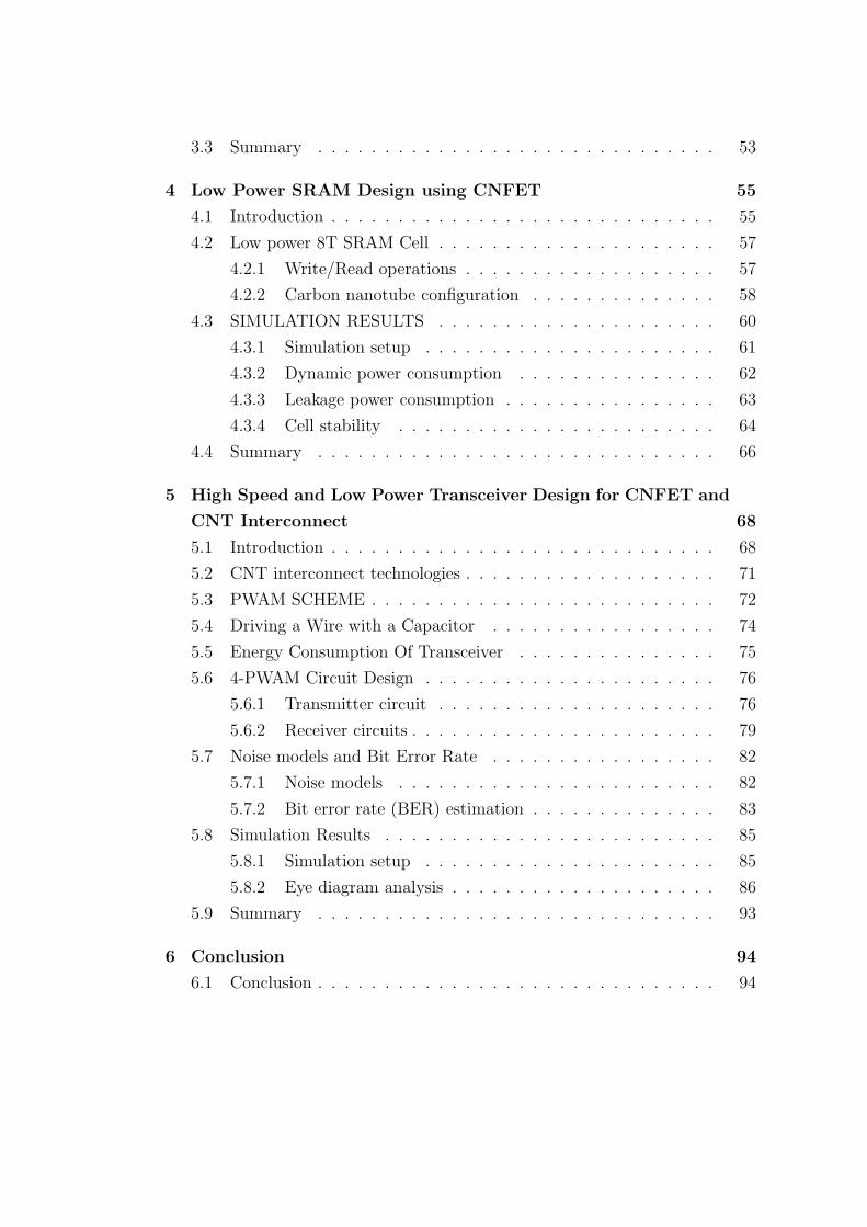
Figure 1.2: Unrolled graphite sheet and the rolled carbon nanotube lattice struc-ture.
1.2 Carbon Nanotube Field-Effect Transistors
As one of the promising new devices, CNFET avoid most of the fundamental
limitations for traditional silicon devices. All the carbon atoms in CNT are
bonded to each other with sp2 hybridization and there is no dangling bond which
enables the integration with high-k dielectric materials. In the next section, we
will introduce the basic properties of CNFET.
1.2.1 Carbon nanotube
A single-walled carbon nanotube (SWCNT) can be visualized as a sheet of
graphite which is rolled up and joined together along a wrapping vector Ch =
n1a1 + n2a2 , where [a1, a2 ] are lattice unit vectors as shown by Fig 1.2, and
the indices (n1, n2) are positive integers that specify the chirality of the tube
[9]. The length of Ch is thus the circumference of the CNT, which is given by,
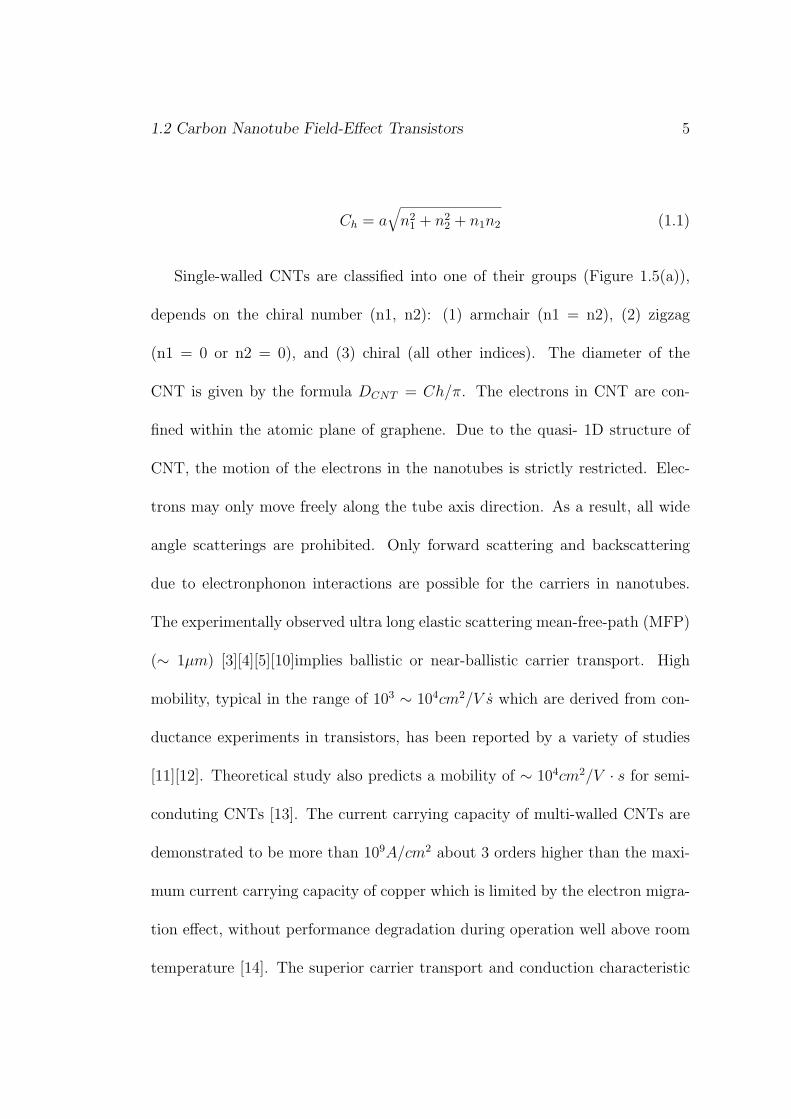
1.2 Carbon Nanotube Field-Effect Transistors 5
Ch = a√n21 + n2
2 + n1n2 (1.1)
Single-walled CNTs are classified into one of their groups (Figure 1.5(a)),
depends on the chiral number (n1, n2): (1) armchair (n1 = n2), (2) zigzag
(n1 = 0 or n2 = 0), and (3) chiral (all other indices). The diameter of the
CNT is given by the formula DCNT = Ch/π. The electrons in CNT are con-
fined within the atomic plane of graphene. Due to the quasi- 1D structure of
CNT, the motion of the electrons in the nanotubes is strictly restricted. Elec-
trons may only move freely along the tube axis direction. As a result, all wide
angle scatterings are prohibited. Only forward scattering and backscattering
due to electronphonon interactions are possible for the carriers in nanotubes.
The experimentally observed ultra long elastic scattering mean-free-path (MFP)
(∼ 1µm) [3][4][5][10]implies ballistic or near-ballistic carrier transport. High
mobility, typical in the range of 103 ∼ 104cm2/V s which are derived from con-
ductance experiments in transistors, has been reported by a variety of studies
[11][12]. Theoretical study also predicts a mobility of ∼ 104cm2/V · s for semi-
conduting CNTs [13]. The current carrying capacity of multi-walled CNTs are
demonstrated to be more than 109A/cm2 about 3 orders higher than the maxi-
mum current carrying capacity of copper which is limited by the electron migra-
tion effect, without performance degradation during operation well above room
temperature [14]. The superior carrier transport and conduction characteristic
1.2 Carbon Nanotube Field-Effect Transistors 6
makes CNTs desirable for nanoelectronics applications, e.g. interconnect and
nanoscale devices.
1.2.2 CNFET
The operation principle of carbon nanotube field-effect transistor (CNFET) is
similar to that of traditional silicon devices. This three (or four) terminal device
consists of a semiconduting nanotube, acting as conducting channel, bridging the
source and drain contacts. The device is turned on or off electrostatically via the
gate. The quasi-1D device structure provides better gate electrostatic control
over the channel region than 3D device (e.g. bulk CMOS) and 2D device (e.g.
fully depleted SOI) structures [15]. In terms of the device operation mechanism,
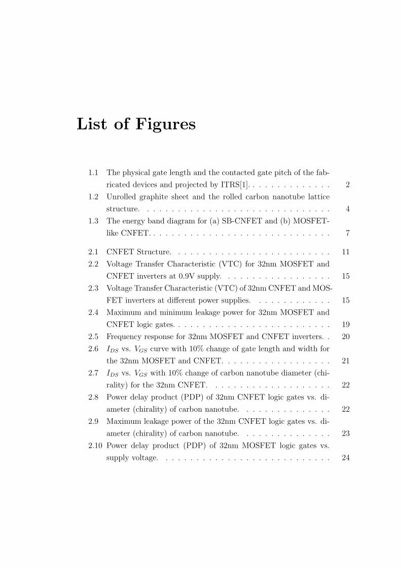
CNFET can be categorized as either Schottky Barrier (SB) controlled FET (SB-
CNFET) or MOSFET-like FET[3][4][16]. The conductivity of SB-CNFET is
governed by the majority carriers tunneling through the SBs at the end contacts.
The on-current and thereby device performance of SB-CNFET is determined
by the contact resistance due to the presence of tunneling barriers at both or
one of the source and drain contacts, instead of the channel conductance, as
shown by Fig 1.3(a). The SBs at source/drain contacts are due to the Fermi-
level alignment at the metal-semiconductor interface. Both the height and the
width of the SBs, and therefore the conductivity, are modulated by the gate
electrostatically. SB-CNFET shows ambipolar transport behavior [18]. The
1.3 Thesis Outline 7
(a) SB-CNFET (b) MOSFET-like CNFET
Figure 1.3: The energy band diagram for (a) SB-CNFET and (b) MOSFET-likeCNFET.
work function induced barriers at the end contacts can be made to enhance
either electron or hole transport. Thus both the device polarity (n-type FET
or p-type FET) and the device bias point can be adjusted by choosing the
appropriate work function of source/drain contacts [17]. On the other hand,
MOSFETlike CNFET exhibits unipolar behavior by suppressing either electron
(pFET) or hole (nFET) transport with heavily doped source/drain. The non-
tunneling potential barrier in the channel region, and thereby the conductivity,
is modulated by the gate-source bias (Fig 1.3(b)).
1.3 Thesis Outline
Significant efforts have been made in recent years to model and simulate CNT
based devices such as the CNFET [2] and a CNT interconnect [21]. However,
these efforts have been concentrated mostly at a device-level. However, the
dynamic performance of a circuit made of multiple CNFETs and an interconnect
1.3 Thesis Outline 8
has not been properly addressed in the technical literature. Therefore, it is
valuable to propose circuit level design methodology for CNFET technology.
This thesis focuses on low power and high speed circuit design issues for CNFET
technology and evaluation of nanoscale devices and circuits including the realistic
device structures, device/circuit non-idealities and process related imperfections.
This thesis is organized as follows ;
In chapter 2, a detailed performance analysis and comparison between CN-
FETs and bulk nano CMOS technologies are undertaken at circuit-level for high
performance and low power dissipation. Logic gates and benchmark circuits are
investigated for performance, energy efficiency, and leakage current under dif-
ferent operational conditions by considering process, power supply voltage, and
temperature (PVT) variations. After performance comparison with conventional
CMOS.
In chapter 3, The characteristics of CNFET is analyzed and novel circuit
design methodology for CNFET based combinational circuits is proposed; this
methodology considers channel capacitance and current variations to determine
optimum PDP(power delay product) value, circuit speed and area.
In chapter 4, As an application of memory circuit, 8T SRAM structure
which strengthens the advantages of CNFET is proposed. This proposed de-
sign method improves SNM, and lowers the power.
Chapter 5 presents low power and high speed transceiver design method wit
1.3 Thesis Outline 9
CNFET and CNT bundle wire. The explanation for capacitive driven wire and
PWAM (pulse width amplitude modulation) scheme is in chapter5. Combining
CNFET and CNT technologies to PWAM and capacitive driven wire scheme
hight speed and low power transceiver is implemented. The implementation in-
cludes new circuits which consist of PWAM modulation blocks. In order to eval-
uate in realistic environment, various noise modeling and bit error rate (BER)
estimation is taken.
In chapter 6, this thesis conclusion are addressed.
Chapter 2
Analysis of CNFET Technology
2.1 CNFET Technology
CNTs are sheets of graphene rolled into tubes; depending on the chirality (i.e.,
the direction in which the grapheme sheet is rolled), a single-walled CNT can
be either metallic or semiconducting. Semiconducting nanotubes have attracted
widespread attention of device/circuit designers as an alternative possible chan-
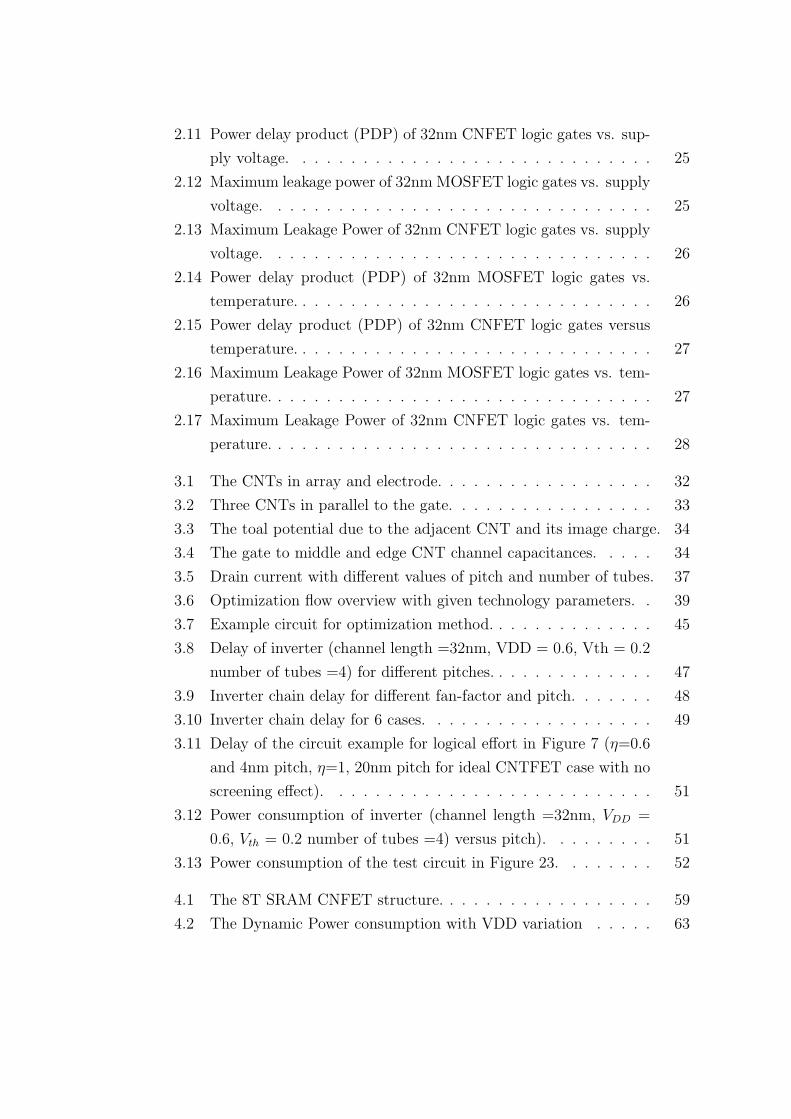
nel implementation for high-performance transistors [22]. A typical structure
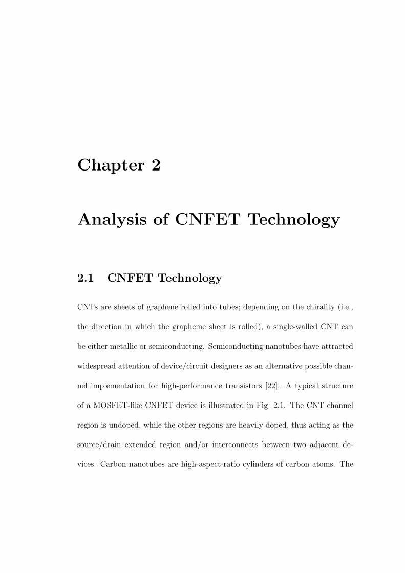
of a MOSFET-like CNFET device is illustrated in Fig 2.1. The CNT channel
region is undoped, while the other regions are heavily doped, thus acting as the
source/drain extended region and/or interconnects between two adjacent de-
vices. Carbon nanotubes are high-aspect-ratio cylinders of carbon atoms. The
2.1 CNFET Technology 11
electrical properties of a single wall carbon nanotube (SWNT) offer the poten-
tial for molecular-scale electronics; a typical semiconducting single-wall carbon
nanotube is 1.4nm in diameter with a 0.6eV bandgap (the bandgap is inversely
proportional to the diameter). Recent carbon nanotube field effect transistors
(CNFETs) have a metal carbide source/drain contact [25] and a top gated struc-
ture (Fig 2.1) with thin gate dielectrics[26].
Figure 2.1: CNFET Structure.
The contact resistance and the subthreshold slope of a CNFET are compara-
ble to those of a silicon MOSFET. While a silicon FETs current drive is typically
measured in current per unit device width (e.g. µA/µm), the CNFETs current
is measured in current per tube (as reflecting the structure of the CNFET as an
array of equal carbon nanotubes with constant spacing and fixed diameter).
2.2 Performance Analysis between CNFET and CMOS Under PVT Variation12
2.2 Performance Analysis between CNFET and
CMOS Under PVT Variation
The CV/I performance of an intrinsic CNFET is 13 times better than the CV/I
performance of a bulk n-type MOSFET because the CNFETs effective gate ca-
pacitance of one CNT per gate is about 4% compared to bulk CMOS and the
driving current ability of each CNT is about 50% of a bulk n-type MOSFET
with minimum gate width (48 nm) at a 32 nm node (due to the ballistic trans-
port nature of a CNT). Moreover due to the similar behavior and the current
driving capability of a pFET compared to those of a nFET, the performance
improvement of a pFET over a PMOS is better than the one of a nFET over
a NMOS. Even though a CNFET has a leakage current in the off-state, this
leakage current is controlled by the full band gap of the CNTs and the band to
band tunneling; this is less than for a MOSFET [26][27].
The expexted (optimistic) performance advantage of a CNFET (as decribed
previously) is unlikely to be achievable in a real device and will be significantly
degraded for the CV/I (6 times for a nFET and 14 times for a pFET) due
to device/circuit non-ideal conditions. These non-ideal conditions include the
series resistance of the doped source/drain region, the Schottky barrier (SB) re-
sistance at the metal/CNT interface, the gate outer-fringe capacitance and the
interconnect wiring capacitance. However, the need for low power consumption
2.2 Performance Analysis between CNFET and CMOS Under PVT Variation13
and high operating frequency has resulted in geometry and supply scaling with
a significant increase in operating temperature for a device. With these scal-
ing features, the effects of systematic and random variations in process, supply
voltage, and temperature (PVT) may cause an inconsistent delay and increase
in leakage to appear even in low power circuits, thus becoming one of the major
challenges in nano scale devices. Therefore, to measure the actual performance
of a CNFET compared to a MOSFET, it is necessary to compare performance at
a circuit level under PVT variations. In this paper, logic gates and benchmark
circuits are designed at 32nm for both CNFET and CMOS technologies; delay,
power, power delay product (PDP), leakage current and frequency response are
simulated and compared [26] [28].
2.2.1 Deciciding ratio between PMOS and NMOS
For comparing the performance of CNFETs with MOSFETs at circuit level, the
inverter as a fundamental logic gate is considered first; the inverter is designed
with minimal width and a number of tubes in 32nm technology. For Si CMOS, a
PMOS/NMOS ratio between 2 and 3 is used for compensating the difference in
mobility between PMOS and NMOS. In this paper, a 3 to 1 (PMOS:NMOS) ratio
is used when designing the inverter because the Voltage Transfer Characteristic
(VTC) of the MOSFET inverter shows a more symmetrical shape in the center
of the logic threshold voltage (VDD/2) for a ratio of 3 in 32nm technology (as
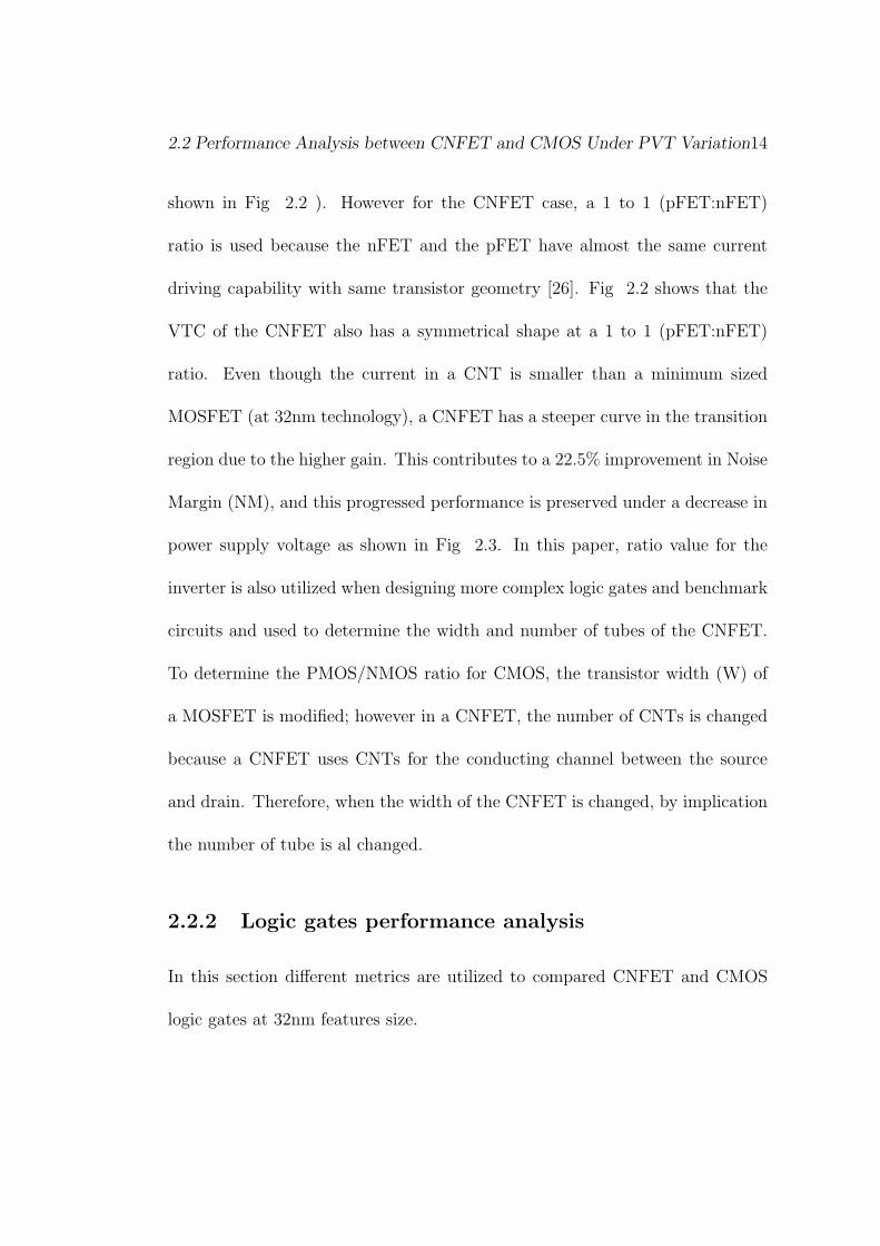
2.2 Performance Analysis between CNFET and CMOS Under PVT Variation14
shown in Fig 2.2 ). However for the CNFET case, a 1 to 1 (pFET:nFET)
ratio is used because the nFET and the pFET have almost the same current
driving capability with same transistor geometry [26]. Fig 2.2 shows that the
VTC of the CNFET also has a symmetrical shape at a 1 to 1 (pFET:nFET)
ratio. Even though the current in a CNT is smaller than a minimum sized
MOSFET (at 32nm technology), a CNFET has a steeper curve in the transition
region due to the higher gain. This contributes to a 22.5% improvement in Noise
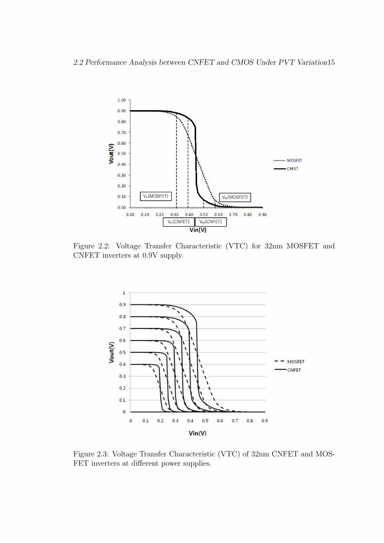
Margin (NM), and this progressed performance is preserved under a decrease in
power supply voltage as shown in Fig 2.3. In this paper, ratio value for the
inverter is also utilized when designing more complex logic gates and benchmark
circuits and used to determine the width and number of tubes of the CNFET.
To determine the PMOS/NMOS ratio for CMOS, the transistor width (W) of
a MOSFET is modified; however in a CNFET, the number of CNTs is changed
because a CNFET uses CNTs for the conducting channel between the source
and drain. Therefore, when the width of the CNFET is changed, by implication
the number of tube is al changed.
2.2.2 Logic gates performance analysis
In this section different metrics are utilized to compared CNFET and CMOS
logic gates at 32nm features size.
2.2 Performance Analysis between CNFET and CMOS Under PVT Variation15
Figure 2.2: Voltage Transfer Characteristic (VTC) for 32nm MOSFET andCNFET inverters at 0.9V supply.
Figure 2.3: Voltage Transfer Characteristic (VTC) of 32nm CNFET and MOS-FET inverters at different power supplies.
2.2 Performance Analysis between CNFET and CMOS Under PVT Variation16
Power Delay Product (PDP)
Due to the increased demand for high-speed, high-throughput computation, and
complex functionality in mobile environments, reduction of delay and power
consumption is very challenging. MOSFET and CNFET can be compared using
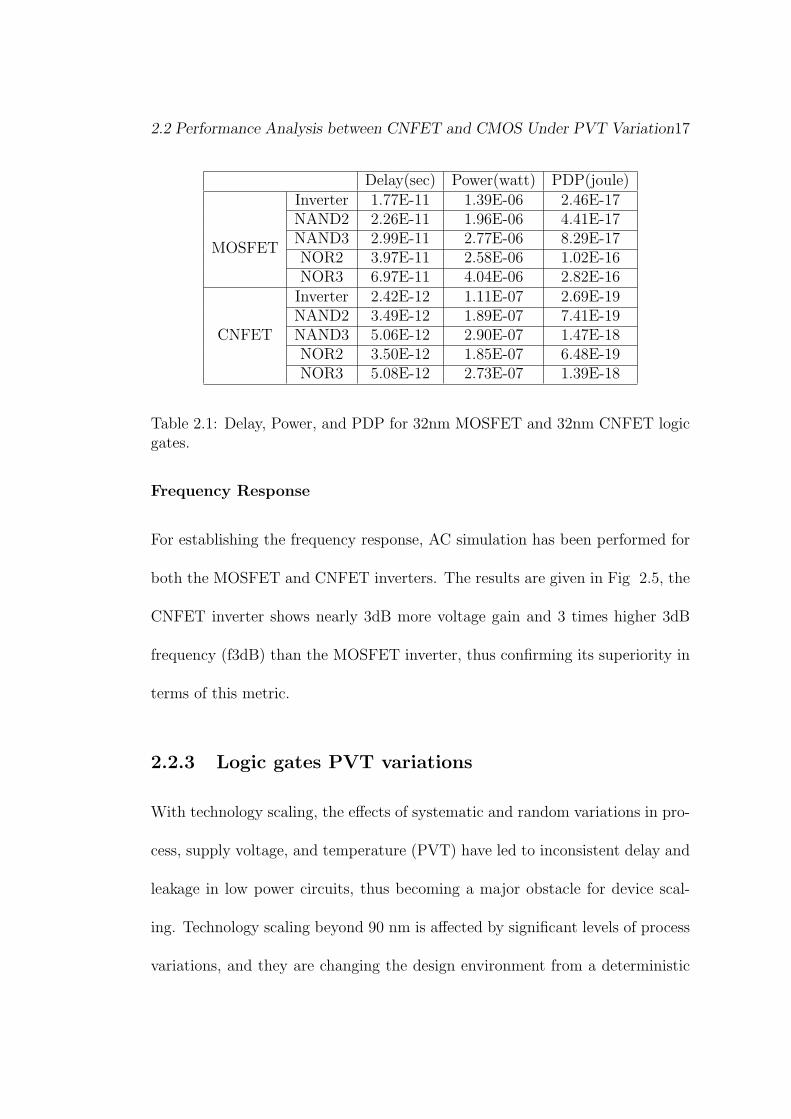
the Power Delay Product (PDP) as metric. Table 2.1 shows the delay, power,
and Power Delay Product (PDP) of logic gates in 32nm MOSFET and 32nm
CNFET technologies; the PDP of the 32nm MOSFET is about 100 times higher
than that of the 32nm CNFET.
Leakage
As process dimensions shrink further into the nanometer ranges, traditional
methods for dynamic power reduction are becoming less effective due to the
increased impact of static power [29]. In general, leakage power is different
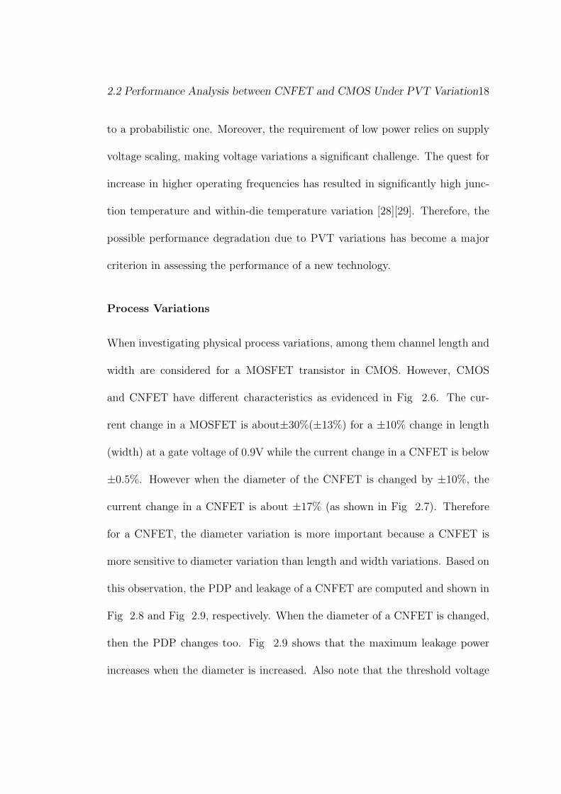
depending on the applied input vector. Fig 2.4 shows the maximum and min-
imum leakage power for 32nm MOSFET and CNFET-based logic gates. The
maximum leakage power of the MOSFET-based gates is 75 times larger than
for CNFET gates. The minimum leakage power of the MOSFET is about three
times larger than for CNFET. Fig 2.4 also shows that the maximum leakage
power shows a similar trend for both CNFET and MOSFET-based gates, while
the minimum leakage power shows somewhat different trends, because the stack
effect is reduced in CNFET circuits .
2.2 Performance Analysis between CNFET and CMOS Under PVT Variation17
Delay(sec) Power(watt) PDP(joule)
MOSFET
Inverter 1.77E-11 1.39E-06 2.46E-17NAND2 2.26E-11 1.96E-06 4.41E-17NAND3 2.99E-11 2.77E-06 8.29E-17NOR2 3.97E-11 2.58E-06 1.02E-16NOR3 6.97E-11 4.04E-06 2.82E-16
CNFET
Inverter 2.42E-12 1.11E-07 2.69E-19NAND2 3.49E-12 1.89E-07 7.41E-19NAND3 5.06E-12 2.90E-07 1.47E-18NOR2 3.50E-12 1.85E-07 6.48E-19NOR3 5.08E-12 2.73E-07 1.39E-18
Table 2.1: Delay, Power, and PDP for 32nm MOSFET and 32nm CNFET logicgates.
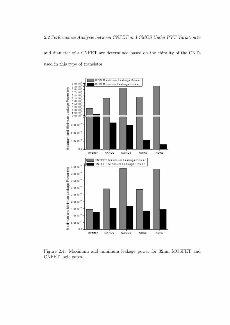
Frequency Response
For establishing the frequency response, AC simulation has been performed for
both the MOSFET and CNFET inverters. The results are given in Fig 2.5, the
CNFET inverter shows nearly 3dB more voltage gain and 3 times higher 3dB
frequency (f3dB) than the MOSFET inverter, thus confirming its superiority in
terms of this metric.
2.2.3 Logic gates PVT variations
With technology scaling, the effects of systematic and random variations in pro-
cess, supply voltage, and temperature (PVT) have led to inconsistent delay and
leakage in low power circuits, thus becoming a major obstacle for device scal-
ing. Technology scaling beyond 90 nm is affected by significant levels of process
variations, and they are changing the design environment from a deterministic
2.2 Performance Analysis between CNFET and CMOS Under PVT Variation18
to a probabilistic one. Moreover, the requirement of low power relies on supply
voltage scaling, making voltage variations a significant challenge. The quest for
increase in higher operating frequencies has resulted in significantly high junc-
tion temperature and within-die temperature variation [28][29]. Therefore, the
possible performance degradation due to PVT variations has become a major
criterion in assessing the performance of a new technology.
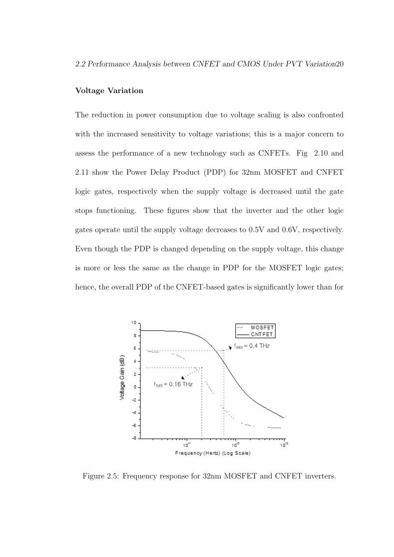
Process Variations
When investigating physical process variations, among them channel length and
width are considered for a MOSFET transistor in CMOS. However, CMOS
and CNFET have different characteristics as evidenced in Fig 2.6. The cur-
rent change in a MOSFET is about±30%(±13%) for a ±10% change in length
(width) at a gate voltage of 0.9V while the current change in a CNFET is below
±0.5%. However when the diameter of the CNFET is changed by ±10%, the
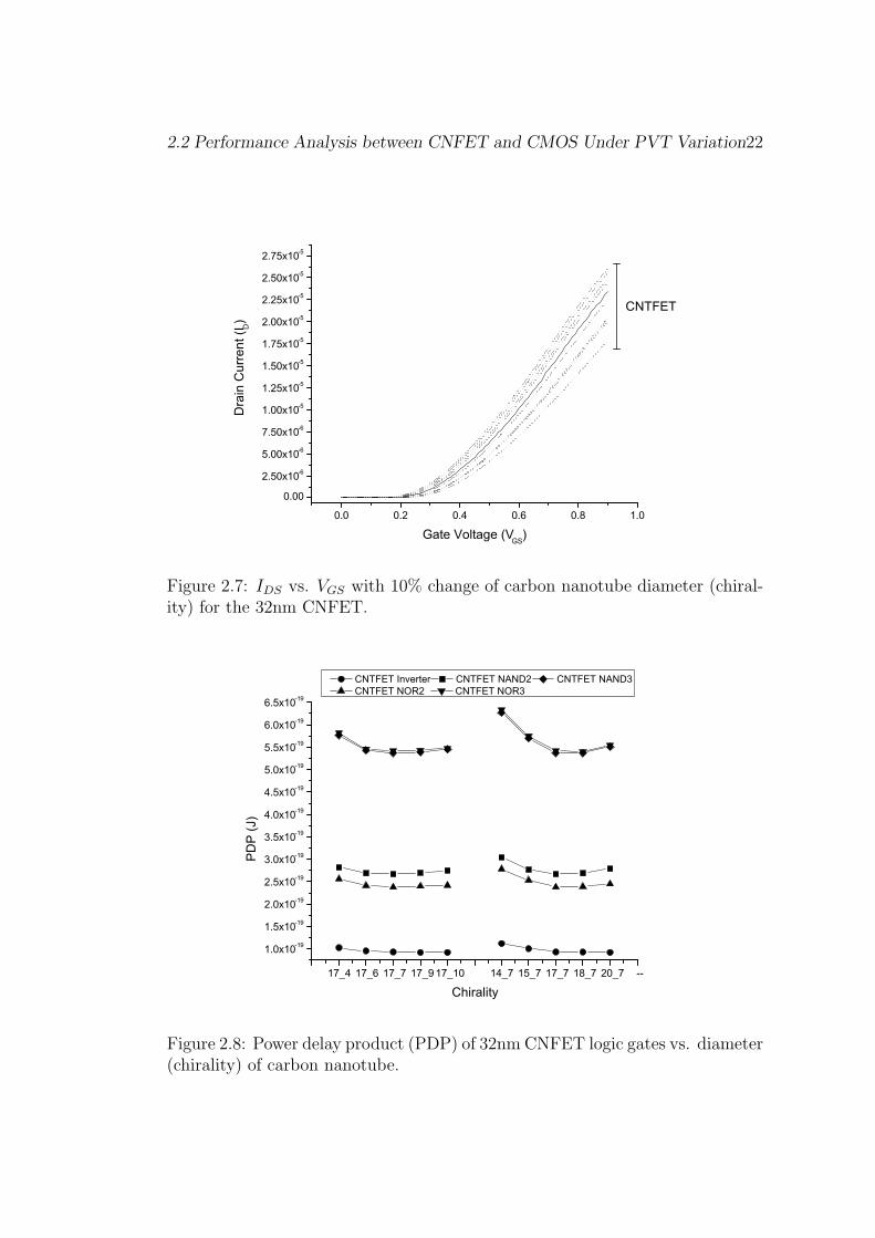
current change in a CNFET is about ±17% (as shown in Fig 2.7). Therefore
for a CNFET, the diameter variation is more important because a CNFET is
more sensitive to diameter variation than length and width variations. Based on
this observation, the PDP and leakage of a CNFET are computed and shown in
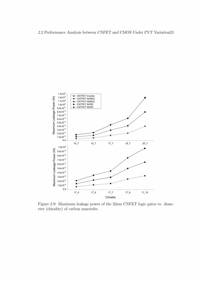
Fig 2.8 and Fig 2.9, respectively. When the diameter of a CNFET is changed,
then the PDP changes too. Fig 2.9 shows that the maximum leakage power
increases when the diameter is increased. Also note that the threshold voltage
2.2 Performance Analysis between CNFET and CMOS Under PVT Variation19
and diameter of a CNFET are determined based on the chirality of the CNTs
used in this type of transistor.
Figure 2.4: Maximum and minimum leakage power for 32nm MOSFET andCNFET logic gates.
2.2 Performance Analysis between CNFET and CMOS Under PVT Variation20
Voltage Variation
The reduction in power consumption due to voltage scaling is also confronted
with the increased sensitivity to voltage variations; this is a major concern to
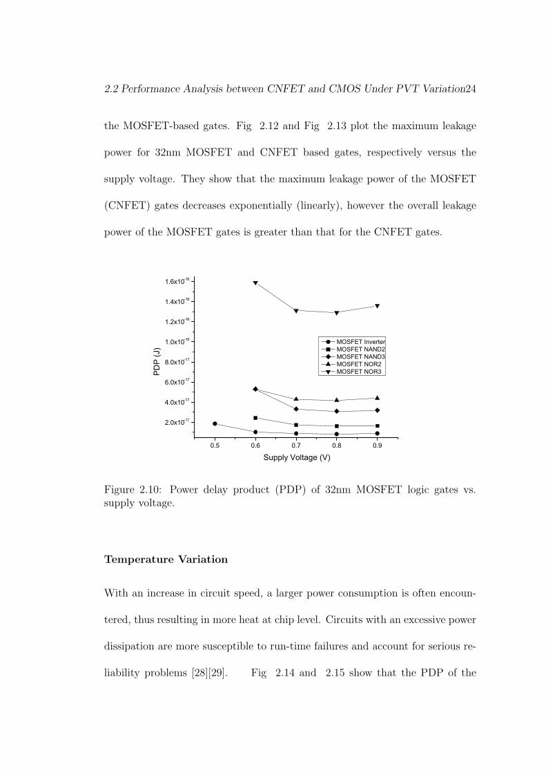
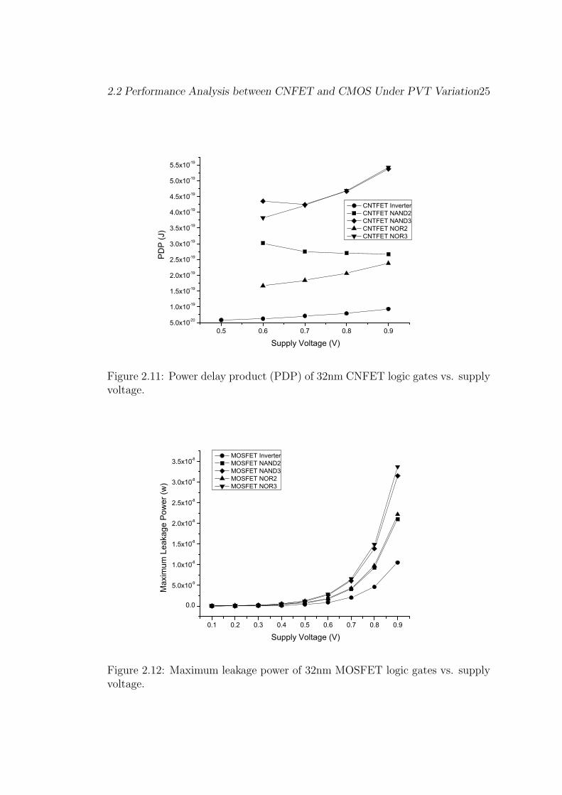
assess the performance of a new technology such as CNFETs. Fig 2.10 and
2.11 show the Power Delay Product (PDP) for 32nm MOSFET and CNFET
logic gates, respectively when the supply voltage is decreased until the gate
stops functioning. These figures show that the inverter and the other logic
gates operate until the supply voltage decreases to 0.5V and 0.6V, respectively.
Even though the PDP is changed depending on the supply voltage, this change
is more or less the same as the change in PDP for the MOSFET logic gates;
hence, the overall PDP of the CNFET-based gates is significantly lower than for
Figure 2.5: Frequency response for 32nm MOSFET and CNFET inverters.
2.2 Performance Analysis between CNFET and CMOS Under PVT Variation21
Figure 2.6: IDS vs. VGS curve with 10% change of gate length and width for the32nm MOSFET and CNFET.
2.2 Performance Analysis between CNFET and CMOS Under PVT Variation22
0.0 0.2 0.4 0.6 0.8 1.0
0.00
2.50x10-65.00x10-67.50x10-61.00x10-51.25x10-51.50x10-51.75x10-52.00x10-52.25x10-52.50x10-52.75x10⁻⁵
CNTFET
Dra
in C
urre
nt (I
D)
Gate Voltage (VGS)
Figure 2.7: IDS vs. VGS with 10% change of carbon nanotube diameter (chiral-ity) for the 32nm CNFET.
17_4 17_6 17_7 17_917_10 14_7 15_7 17_7 18_7 20_7 --
1.0x10-191.5x10-192.0x10-192.5x10-193.0x10-193.5x10-194.0x10-194.5x10-195.0x10-195.5x10-196.0x10-196.5x10⁻¹⁹
CNTFET Inverter CNTFET NAND2 CNTFET NAND3 CNTFET NOR2 CNTFET NOR3
PD
P (J
)
Chirality
Figure 2.8: Power delay product (PDP) of 32nm CNFET logic gates vs. diameter(chirality) of carbon nanotube.
2.2 Performance Analysis between CNFET and CMOS Under PVT Variation23
17_4 17_6 17_7 17_9 17_100.0
1.0x10-102.0x10-103.0x10-104.0x10-105.0x10-106.0x10-107.0x10-108.0x10-109.0x10-101.0x10⁻⁹
Chirality
14_7 15_7 17_7 18_7 20_70.0
1.0x10-102.0x10-103.0x10-104.0x10-105.0x10-106.0x10-107.0x10-108.0x10-109.0x10-101.0x10-91.1x10-91.2x10-91.3x10-9
Max
imum
Lea
kage
Pow
er (W
)M
axim
um L
eaka
ge P
ower
(W) CNTFET Inverter
CNTFET NAND2 CNTFET NAND3 CNTFET NOR2 CNTFET NOR3
Figure 2.9: Maximum leakage power of the 32nm CNFET logic gates vs. diam-eter (chirality) of carbon nanotube.
2.2 Performance Analysis between CNFET and CMOS Under PVT Variation24
the MOSFET-based gates. Fig 2.12 and Fig 2.13 plot the maximum leakage
power for 32nm MOSFET and CNFET based gates, respectively versus the
supply voltage. They show that the maximum leakage power of the MOSFET
(CNFET) gates decreases exponentially (linearly), however the overall leakage
power of the MOSFET gates is greater than that for the CNFET gates.
0.5 0.6 0.7 0.8 0.9
2.0x10⁻¹⁷
4.0x10⁻¹⁷
6.0x10⁻¹⁷
8.0x10⁻¹⁷
1.0x10⁻¹⁶
1.2x10⁻¹⁶
1.4x10⁻¹⁶
1.6x10⁻¹⁶
MOSFET Inverter MOSFET NAND2 MOSFET NAND3 MOSFET NOR2 MOSFET NOR3P
DP
(J)
Supply Voltage (V)
Figure 2.10: Power delay product (PDP) of 32nm MOSFET logic gates vs.supply voltage.
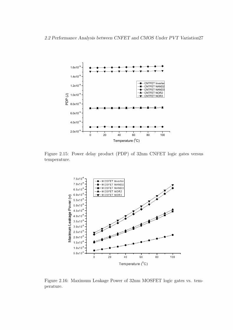
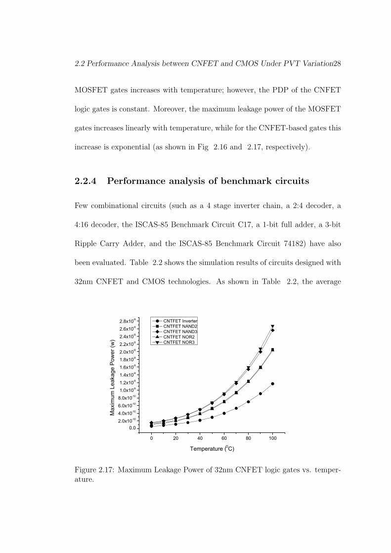
Temperature Variation
With an increase in circuit speed, a larger power consumption is often encoun-
tered, thus resulting in more heat at chip level. Circuits with an excessive power
dissipation are more susceptible to run-time failures and account for serious re-
liability problems [28][29]. Fig 2.14 and 2.15 show that the PDP of the
2.2 Performance Analysis between CNFET and CMOS Under PVT Variation25
0.5 0.6 0.7 0.8 0.95.0x10-20
1.0x10⁻¹⁹
1.5x10⁻¹⁹
2.0x10⁻¹⁹
2.5x10⁻¹⁹
3.0x10⁻¹⁹
3.5x10⁻¹⁹
4.0x10⁻¹⁹
4.5x10⁻¹⁹
5.0x10⁻¹⁹
5.5x10⁻¹⁹
CNTFET Inverter CNTFET NAND2 CNTFET NAND3 CNTFET NOR2 CNTFET NOR3
PD
P (J
)
Supply Voltage (V)
Figure 2.11: Power delay product (PDP) of 32nm CNFET logic gates vs. supplyvoltage.
0.1 0.2 0.3 0.4 0.5 0.6 0.7 0.8 0.9
0.0
5.0x10⁻⁹
1.0x10⁻⁸
1.5x10⁻⁸
2.0x10⁻⁸
2.5x10⁻⁸
3.0x10⁻⁸
3.5x10⁻⁸ MOSFET Inverter MOSFET NAND2 MOSFET NAND3 MOSFET NOR2 MOSFET NOR3
Max
imum
Lea
kage
Pow
er (w
)
Supply Voltage (V)
Figure 2.12: Maximum leakage power of 32nm MOSFET logic gates vs. supplyvoltage.
2.2 Performance Analysis between CNFET and CMOS Under PVT Variation26
0.1 0.2 0.3 0.4 0.5 0.6 0.7 0.8 0.90.0
5.0x10⁻¹¹
1.0x10⁻¹⁰
1.5x10⁻¹⁰
2.0x10⁻¹⁰
2.5x10⁻¹⁰
3.0x10⁻¹⁰
3.5x10⁻¹⁰
4.0x10⁻¹⁰
4.5x10⁻¹⁰
5.0x10⁻¹⁰ CNTFET Inverter CNTFET NAND2 CNTFET NAND3 CNTFET NOR2 CNTFET NOR3
Max
imum
Lea
kage
Pow
er (w
)
Supply Voltage (V)
Figure 2.13: Maximum Leakage Power of 32nm CNFET logic gates vs. supplyvoltage.
Figure 2.14: Power delay product (PDP) of 32nm MOSFET logic gates vs.temperature.
2.2 Performance Analysis between CNFET and CMOS Under PVT Variation27
0 20 40 60 80 1002.0x10-19
4.0x10⁻¹⁹
6.0x10⁻¹⁹
8.0x10⁻¹⁹
1.0x10⁻¹⁸
1.2x10⁻¹⁸
1.4x10⁻¹⁸
1.6x10⁻¹⁸
CNTFET Inverter CNTFET NAND2 CNTFET NAND3 CNTFET NOR2 CNTFET NOR3
PD
P (J
)
Temperature (OC)
Figure 2.15: Power delay product (PDP) of 32nm CNFET logic gates versustemperature.
Figure 2.16: Maximum Leakage Power of 32nm MOSFET logic gates vs. tem-perature.
2.2 Performance Analysis between CNFET and CMOS Under PVT Variation28
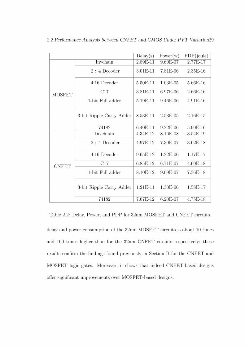
MOSFET gates increases with temperature; however, the PDP of the CNFET
logic gates is constant. Moreover, the maximum leakage power of the MOSFET
gates increases linearly with temperature, while for the CNFET-based gates this
increase is exponential (as shown in Fig 2.16 and 2.17, respectively).
2.2.4 Performance analysis of benchmark circuits
Few combinational circuits (such as a 4 stage inverter chain, a 2:4 decoder, a
4:16 decoder, the ISCAS-85 Benchmark Circuit C17, a 1-bit full adder, a 3-bit
Ripple Carry Adder, and the ISCAS-85 Benchmark Circuit 74182) have also
been evaluated. Table 2.2 shows the simulation results of circuits designed with
32nm CNFET and CMOS technologies. As shown in Table 2.2, the average
0 20 40 60 80 100
0.02.0x10-104.0x10-106.0x10-108.0x10-101.0x10-91.2x10-91.4x10-91.6x10-91.8x10-92.0x10-92.2x10-92.4x10-92.6x10-92.8x10-9 CNTFET Inverter
CNTFET NAND2 CNTFET NAND3 CNTFET NOR2 CNTFET NOR3
Max
imum
Lea
kage
Pow
er (w
)
Temperature (OC)
Figure 2.17: Maximum Leakage Power of 32nm CNFET logic gates vs. temper-ature.
2.2 Performance Analysis between CNFET and CMOS Under PVT Variation29
Delay(s) Power(w) PDP(joule)
MOSFET
Invchain 2.89E-11 9.60E-07 2.77E-17
2 : 4 Decoder 3.01E-11 7.81E-06 2.35E-16
4:16 Decoder 5.50E-11 1.03E-05 5.66E-16
C17 3.81E-11 6.97E-06 2.66E-16
1-bit Full adder 5.19E-11 9.46E-06 4.91E-16
3-bit Ripple Carry Adder 8.53E-11 2.53E-05 2.16E-15
74182 6.40E-11 9.22E-06 5.90E-16
CNFET
Invchiain 4.34E-12 8.16E-08 3.54E-19
2 : 4 Decoder 4.97E-12 7.30E-07 3.62E-18
4:16 Decoder 9.65E-12 1.22E-06 1.17E-17
C17 6.85E-12 6.71E-07 4.60E-18
1-bit Full adder 8.10E-12 9.09E-07 7.36E-18
3-bit Ripple Carry Adder 1.21E-11 1.30E-06 1.58E-17
74182 7.67E-12 6.20E-07 4.75E-18
Table 2.2: Delay, Power, and PDP for 32nm MOSFET and CNFET circuits.
delay and power consumption of the 32nm MOSFET circuits is about 10 times
and 100 times higher than for the 32nm CNFET circuits respectively; these
results confirm the findings found previously in Section B for the CNFET and
MOSFET logic gates. Moreover, it shows that indeed CNFET-based designs
offer significant improvements over MOSFET-based designs.
Chapter 3
Optimization Method for
Combinational CNFET Circuit
In this section the optimal combinational circuit design method for CNTFET is
shown. In section 3.1, a brief review focusing on a CNTFET inclusive of device
characteristics and physical features is provided. In section 3.2, a performance
analysis is pursued for comparison with nano scale CMOS technology. Section
3.3 describes a novel circuit design methodology for CNTFET based circuits; this
methodology considers channel capacitance and current variations to determine
the best pitch, circuit speed and area. Simulation results are also presented to
compare the results obtained by using the proposed methodology with the ones
in which circuits were not optimized (such as for the case of either a too large
or small screening effect due to an incorrect selection of the pitch).
3.1 Analysis of Technology Parameters 31
3.1 Analysis of Technology Parameters
In this section, a design approach for CNTFET-based circuits is presented with
emphasis on the differences with CMOS. For CMOS technology, the gate capac-
itance is proportional to WL (where W is the channel width and L is the channel
length). In CNTFET technology, the gate capacitance depends on the number
of tubes and the pitch (where the pitch is defined as the distance between the
centers of two adjacent CNTs in the same device[30] ). As the pitch decreases,
the gate capacitance is also reduced due to the potential between adjacent CNTs
(affecting the total gate capacitance). Moreover, the pitch also affects the cur-
rent in the CNTFETs. Due to the screening effect [30], the total current of a
CNTFET decreases as the pitch decreases. By analyzing the device character-
istics of a CNTFET, performance metrics such as high speed, low power and
low area overhead can be achieved when designing circuits using this technology.
This aspect will be analyzed further in the next sections.
3.1.1 Channel and gate capacitance vs pitch
To calculate the coupling capacitance C01 consider Fig 3.1; the effects of two
tubes around tube 1 can be lumped into the equivalent capacities of tube 2 and
tube 3 (denoted as C02 and C03 respectively [13]). By applying the same voltage
V1 between tubes 1, 2 and 3 and the electrode, the charges Q1, η1Q1, andη2Q1
are induced on these tubes due to the different coupling capacitances C01, C02,
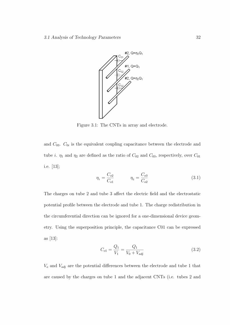
3.1 Analysis of Technology Parameters 32
Figure 3.1: The CNTs in array and electrode.
and C03. C0i is the equivalent coupling capacitance between the electrode and
tube i. η1 and η2 are defined as the ratio of C02 and C03, respectively, over C01
i.e. [13];
η1 =Co2
Co1
η2 =Co3
Co2
(3.1)
The charges on tube 2 and tube 3 affect the electric field and the electrostatic
potential profile between the electrode and tube 1. The charge redistribution in
the circumferential direction can be ignored for a one-dimensional device geom-
etry. Using the superposition principle, the capacitance C01 can be expressed
as [13]:
Co1 =Q1
V1
=Q1
V0 + Vadj
(3.2)
Vo and Vadj are the potential differences between the electrode and tube 1 that
are caused by the charges on tube 1 and the adjacent CNTs (i.e. tubes 2 and
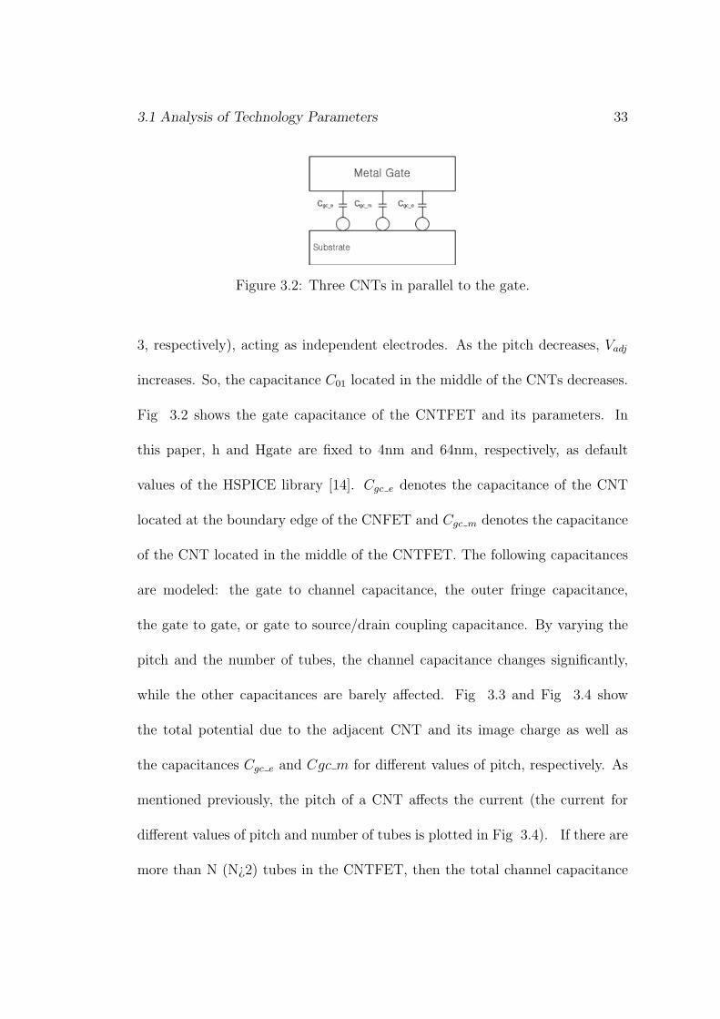
3.1 Analysis of Technology Parameters 33
Figure 3.2: Three CNTs in parallel to the gate.
3, respectively), acting as independent electrodes. As the pitch decreases, Vadj
increases. So, the capacitance C01 located in the middle of the CNTs decreases.
Fig 3.2 shows the gate capacitance of the CNTFET and its parameters. In
this paper, h and Hgate are fixed to 4nm and 64nm, respectively, as default
values of the HSPICE library [14]. Cgc e denotes the capacitance of the CNT
located at the boundary edge of the CNFET and Cgc m denotes the capacitance
of the CNT located in the middle of the CNTFET. The following capacitances
are modeled: the gate to channel capacitance, the outer fringe capacitance,
the gate to gate, or gate to source/drain coupling capacitance. By varying the
pitch and the number of tubes, the channel capacitance changes significantly,
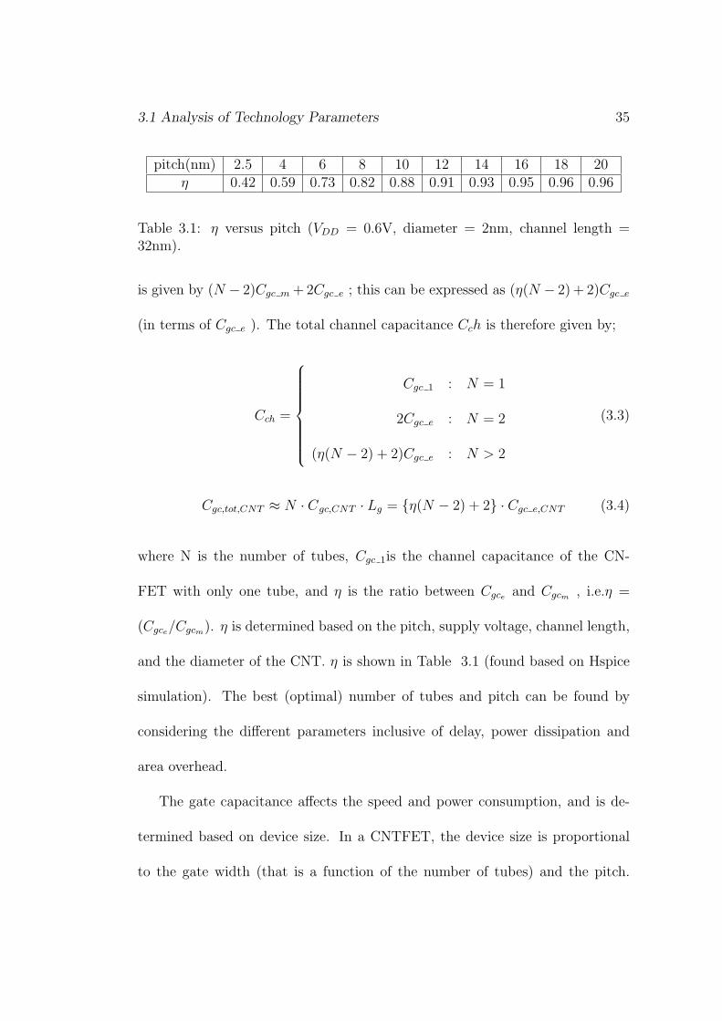
while the other capacitances are barely affected. Fig 3.3 and Fig 3.4 show
the total potential due to the adjacent CNT and its image charge as well as
the capacitances Cgc e and Cgc m for different values of pitch, respectively. As
mentioned previously, the pitch of a CNT affects the current (the current for
different values of pitch and number of tubes is plotted in Fig 3.4). If there are
more than N (N¿2) tubes in the CNTFET, then the total channel capacitance
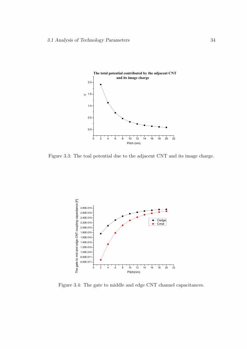
3.1 Analysis of Technology Parameters 34
0 2 4 6 8 10 12 14 16 18 20 22
0.0
0.5
1.0
1.5
2.0
The total potential contributed by the adjacent CNT and its image charge
V
Pitch (nm)
Figure 3.3: The toal potential due to the adjacent CNT and its image charge.
0 2 4 6 8 10 12 14 16 18 20 22
6.00E-011
8.00E-011
1.00E-010
1.20E-010
1.40E-010
1.60E-010
1.80E-010
2.00E-010
2.20E-010
2.40E-010
2.60E-010
2.80E-010
The
gate
to m
id a
nd e
dge
CN
T co
uplin
g ca
paci
tanc
e [F
]
Pitch(nm)
Cedge Cmid
Figure 3.4: The gate to middle and edge CNT channel capacitances.
3.1 Analysis of Technology Parameters 35
pitch(nm) 2.5 4 6 8 10 12 14 16 18 20η 0.42 0.59 0.73 0.82 0.88 0.91 0.93 0.95 0.96 0.96
Table 3.1: η versus pitch (VDD = 0.6V, diameter = 2nm, channel length =32nm).
is given by (N − 2)Cgc m +2Cgc e ; this can be expressed as (η(N − 2) + 2)Cgc e
(in terms of Cgc e ). The total channel capacitance Cch is therefore given by;
Cch =
Cgc 1 : N = 1
2Cgc e : N = 2
(η(N − 2) + 2)Cgc e : N > 2
(3.3)
Cgc,tot,CNT ≈ N · Cgc,CNT · Lg = η(N − 2) + 2 · Cgc e,CNT (3.4)
where N is the number of tubes, Cgc 1is the channel capacitance of the CN-
FET with only one tube, and η is the ratio between Cgce and Cgcm , i.e.η =
(Cgce/Cgcm). η is determined based on the pitch, supply voltage, channel length,
and the diameter of the CNT. η is shown in Table 3.1 (found based on Hspice
simulation). The best (optimal) number of tubes and pitch can be found by
considering the different parameters inclusive of delay, power dissipation and
area overhead.
The gate capacitance affects the speed and power consumption, and is de-
termined based on device size. In a CNTFET, the device size is proportional
to the gate width (that is a function of the number of tubes) and the pitch.
3.1 Analysis of Technology Parameters 36
The CNTFET gate capacitance (Cgate,CNT ) consists of three components [13]:
the gate to channel capacitance (Cgc,tot,CNT ), the gate outer fringe capacitance
(Cfr,tot,CNT ), and the coupling capacitance between the gate and the adjacent
contacts (Cgtg,tot,CNT ). These components are approximated as follows:
Cfr,tot,CNT ≈ Cfr,CNT · Lg (3.5)
Cgtg,tot,CNT = Cgtg ·Wg (3.6)
Cgate,CNT ≈ η(N − 2) + 2 · Cgc e,CNT + Cgtg ·Wg (3.7)
3.1.2 Size of CNFET
The total size of the CNFET is determined by the width of the gate (as for the
device structure of Fig 2.1). The gate width can be determined by the pitch.
By setting the minimum gate width Wmin and the number of tubes N , the gate
width can be approximated as
Wg = Max(Wmin, N · pitch) (3.8)
3.1.3 CNFET threshold voltage
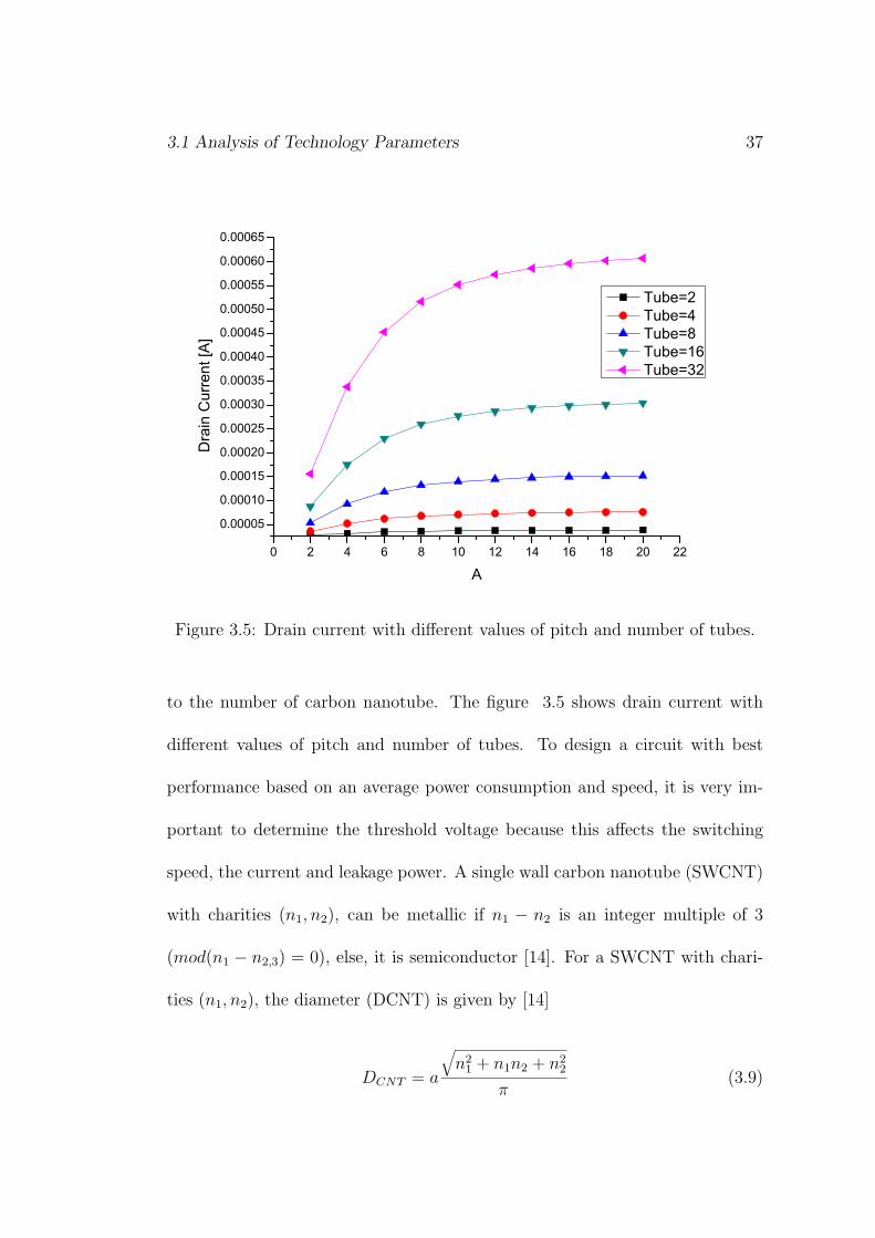
The drain current of the CNTFET is dependent on pitch value, which determine
the amount of screening effect. Therefore the current is not linearly proportional
3.1 Analysis of Technology Parameters 37
0 2 4 6 8 10 12 14 16 18 20 22
0.00005
0.00010
0.00015
0.00020
0.00025
0.00030
0.00035
0.00040
0.00045
0.00050
0.00055
0.00060
0.00065
Dra
in C
urre
nt [A
]
A
Tube=2 Tube=4 Tube=8 Tube=16 Tube=32
Figure 3.5: Drain current with different values of pitch and number of tubes.
to the number of carbon nanotube. The figure 3.5 shows drain current with
different values of pitch and number of tubes. To design a circuit with best
performance based on an average power consumption and speed, it is very im-
portant to determine the threshold voltage because this affects the switching
speed, the current and leakage power. A single wall carbon nanotube (SWCNT)
with charities (n1, n2), can be metallic if n1 − n2 is an integer multiple of 3
(mod(n1 − n2,3) = 0), else, it is semiconductor [14]. For a SWCNT with chari-
ties (n1, n2), the diameter (DCNT) is given by [14]
DCNT = a
√n21 + n1n2 + n2
2
π(3.9)
3.1 Analysis of Technology Parameters 38
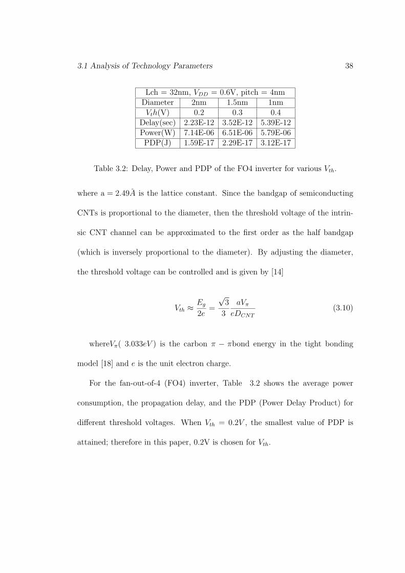
Lch = 32nm, VDD = 0.6V, pitch = 4nmDiameter 2nm 1.5nm 1nmVth(V) 0.2 0.3 0.4
Delay(sec) 2.23E-12 3.52E-12 5.39E-12Power(W) 7.14E-06 6.51E-06 5.79E-06PDP(J) 1.59E-17 2.29E-17 3.12E-17
Table 3.2: Delay, Power and PDP of the FO4 inverter for various Vth.
where a = 2.49A is the lattice constant. Since the bandgap of semiconducting
CNTs is proportional to the diameter, then the threshold voltage of the intrin-
sic CNT channel can be approximated to the first order as the half bandgap
(which is inversely proportional to the diameter). By adjusting the diameter,
the threshold voltage can be controlled and is given by [14]
Vth ≈ Eg
2e=
√3
3
aVπ
eDCNT
(3.10)
whereVπ( 3.033eV ) is the carbon π − πbond energy in the tight bonding
model [18] and e is the unit electron charge.
For the fan-out-of-4 (FO4) inverter, Table 3.2 shows the average power
consumption, the propagation delay, and the PDP (Power Delay Product) for
different threshold voltages. When Vth = 0.2V , the smallest value of PDP is
attained; therefore in this paper, 0.2V is chosen for Vth.
3.2 Performance Opimization Methods 39
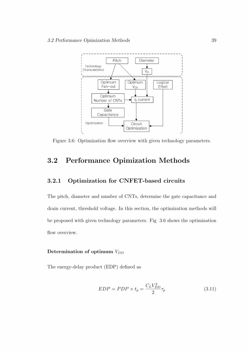
Figure 3.6: Optimization flow overview with given technology parameters.
3.2 Performance Opimization Methods
3.2.1 Optimization for CNFET-based circuits
The pitch, diameter and number of CNTs, determine the gate capacitance and
drain current, threshold voltage. In this section, the optimization methods will
be proposed with given technology parameters. Fig 3.6 shows the optimization
flow overview.
Determination of optimum VDD
The energy-delay product (EDP) defined as
EDP = PDP × tp =CLV
2DD
2τp (3.11)

3.2 Performance Opimization Methods 40
The τp can be approximated as below [19]
τp =Cgg,CNFETVDD
ICNFET
= ηCNT · Cgg,CNFETLgVDD
gCNT (VDD − Vth,CNT − VDSAT/2)(3.12)
Where ICNFET is given by [14]
ICNFET =n · gCNT (VDD − Vth,CNT − VDSAT/2)
1 + gCNTLsρs(3.13)
Where gCNT is the transconductance per CNT, and Ls is the source length
(doped CNT region), ρs is the source resistance per unit length of doped CNT,ηCNT
is the pre-defined technology factor,Cgg,CNFET is gate capacitance. VDSAT is the
voltage which start to saturate the drain. Put τp in 3.12 into 3.11, the EDP
as follow
EDP = PDP × tp =αCL
2V 3DD
2(VDD − Vth− (VDSAT )/2)(3.14)
Taking the derivative equation 3.14 with respect to VDD and equating the result
to 0. The result is
VDD =3
2(Vth + VDSAT/2) (3.15)
In order to find VDSAT , drain current equation of CNT will be used. The drain
current equation is derived from the Landauer formula [18], which describes
ballistic transport with ideal contacts. Its expression represents the sum of the

3.2 Performance Opimization Methods 41
energy sub-band contributions of two terms where ∆p is the minima of the pth
energy sub-band, e is the electron charge, kB the Boltzman constant, h the
Planck constant, and T the temperature.
ID =4ekBT
h
+∞∑p=1
[ln(1 + exp
−∆P + VCNT
kBT
)− ln
(1 + exp
−VDS −∆P + VCNT
kBT
)](3.16)
Since it is not possible to obtain an analytical closed-form expression to calculate
the number of carriers in the channel, ηCNT , the following empirical relationship
has been proposed in [18].
VCNT = VGS forVGS < ∆1
= VGS − α(VGS −∆1) forVGS ≥ ∆1 (3.17)
Where ∆p is the energy level for the first sub-band, and
VCNT = VGS forVGS < ∆1
= VGS − α(VGS −∆1) forVGS ≥ ∆1 (3.18)
α0, 1, 2 are fitting parameters depending on the gate-oxide capacitance, CNT
diameter. Taking the derivative equation 3.14 with respect to VDS equating the
result to approximately 0 , the VDS which saturate the drain current can be
found. With given technology parameters in this work, this VDSAT is almost 0.4
3.2 Performance Opimization Methods 42
V. Therefore, the optimal VDD in this work which obtained from equation 3.15
is about 0.6V.
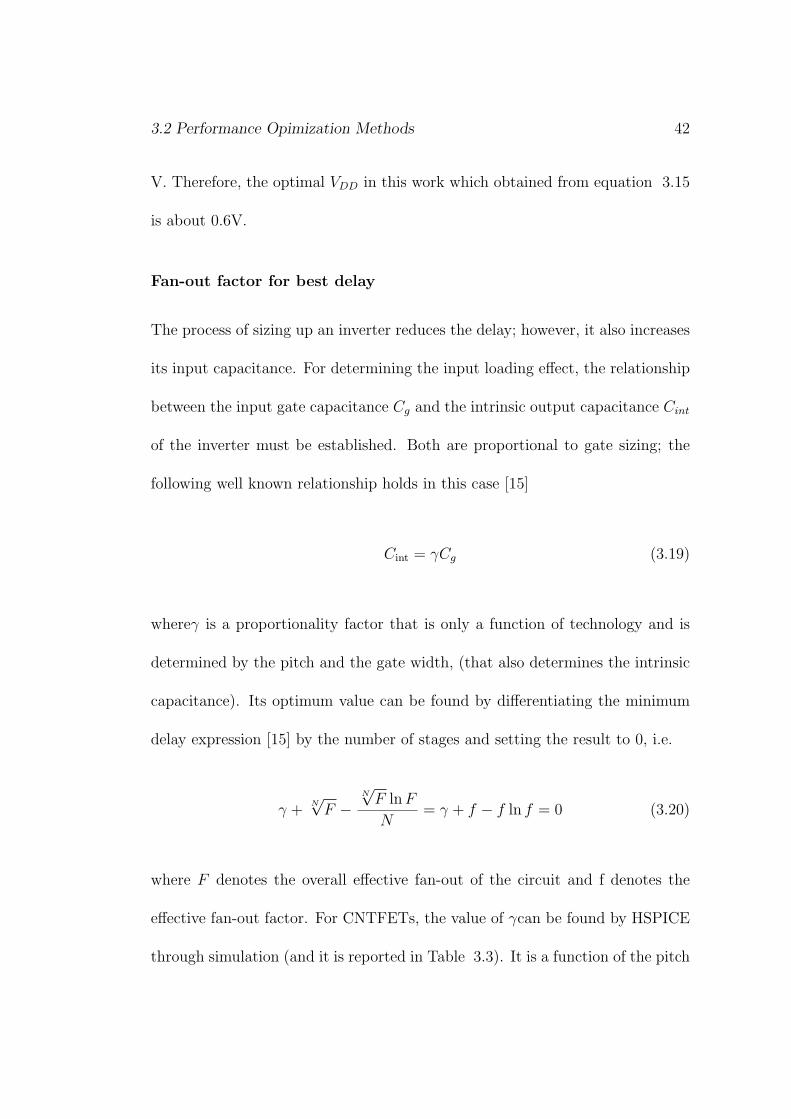
Fan-out factor for best delay
The process of sizing up an inverter reduces the delay; however, it also increases
its input capacitance. For determining the input loading effect, the relationship
between the input gate capacitance Cg and the intrinsic output capacitance Cint
of the inverter must be established. Both are proportional to gate sizing; the
following well known relationship holds in this case [15]
Cint = γCg (3.19)
whereγ is a proportionality factor that is only a function of technology and is
determined by the pitch and the gate width, (that also determines the intrinsic
capacitance). Its optimum value can be found by differentiating the minimum
delay expression [15] by the number of stages and setting the result to 0, i.e.
γ +N√F −
N√F lnF
N= γ + f − f ln f = 0 (3.20)
where F denotes the overall effective fan-out of the circuit and f denotes the
effective fan-out factor. For CNTFETs, the value of γcan be found by HSPICE
through simulation (and it is reported in Table 3.3). It is a function of the pitch
3.2 Performance Opimization Methods 43
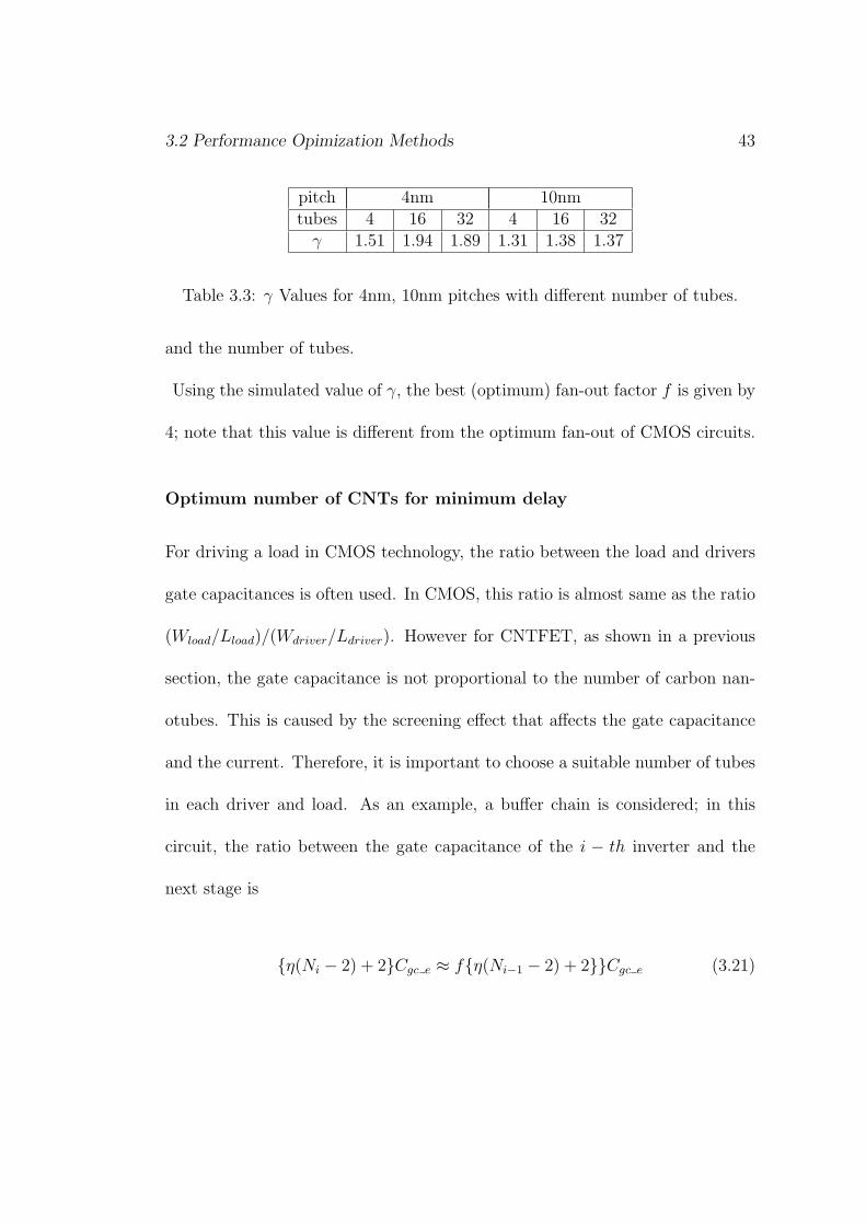
pitch 4nm 10nmtubes 4 16 32 4 16 32γ 1.51 1.94 1.89 1.31 1.38 1.37
Table 3.3: γ Values for 4nm, 10nm pitches with different number of tubes.
and the number of tubes.
Using the simulated value of γ, the best (optimum) fan-out factor f is given by
4; note that this value is different from the optimum fan-out of CMOS circuits.
Optimum number of CNTs for minimum delay
For driving a load in CMOS technology, the ratio between the load and drivers
gate capacitances is often used. In CMOS, this ratio is almost same as the ratio
(Wload/Lload)/(Wdriver/Ldriver). However for CNTFET, as shown in a previous
section, the gate capacitance is not proportional to the number of carbon nan-
otubes. This is caused by the screening effect that affects the gate capacitance
and the current. Therefore, it is important to choose a suitable number of tubes
in each driver and load. As an example, a buffer chain is considered; in this
circuit, the ratio between the gate capacitance of the i − th inverter and the
next stage is
η(Ni − 2) + 2Cgc e ≈ fη(Ni−1 − 2) + 2Cgc e (3.21)

3.2 Performance Opimization Methods 44
CMOS(32nm) Number of inputsLogical effort 2 3 4 n
inverter 1NAND 5/4 6/4 7/4 (n+3)/4NOR 7/4 10/4 13/4 (3n+1)/2
Table 3.4: Logical Effort for CNTFET.
Solving 3.11 for Ni
Ni = f ·Ni−1 + 2
(1− f +
f
η− 1
η
)
= f ·Ni−1 +K(f, η) (3.22)
where K(f, η) = 2(1− f + f
η− 1
η
)Ni denotes the number of carbon nanotubes
of the i − th stage, and f is the effective fan-out factor. K(f, η) is a function
of f and η; the values are determined by the pitch and the number of tubes in
the CNTFET. Based on γ as reported in Table 3.3, in most cases the optimum
value of f is 4 and the value of η can be found from Table 3.1.
Logical effort for combinational logic
The so-called logical effort of a gate denotes the additional input capacitance of
a gate to deliver the same output current as an inverter. The logical effort is an
important figure of merit, because it can be used to reduce the path delay of a
circuit [16].
In a CNTFET, the P-type and N-type have almost the same carrier mobility
3.2 Performance Opimization Methods 45
CMOS(32nm) Number of inputsLogical effort 2 3 4 n
inverter 1NAND 5/4 6/4 7/4 (n+3)/4NOR 7/4 10/4 13/4 (3n+1)/2
Table 3.5: Logical Effort for 32nm CMOS.
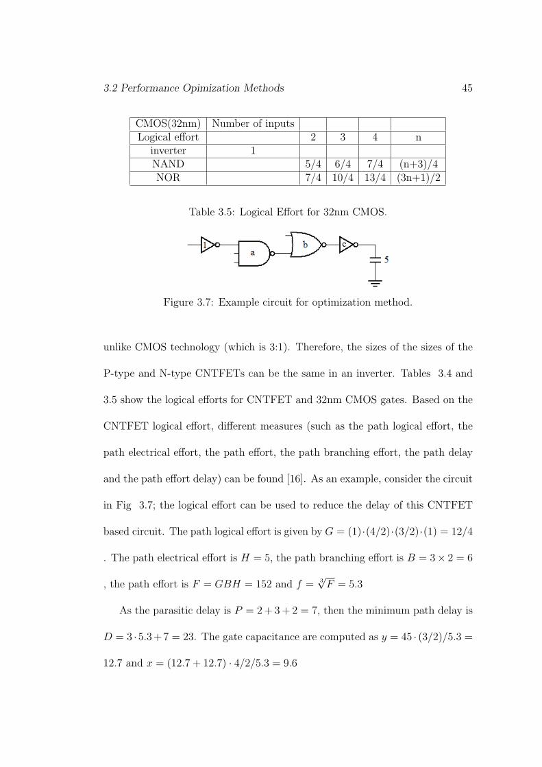
Figure 3.7: Example circuit for optimization method.
unlike CMOS technology (which is 3:1). Therefore, the sizes of the sizes of the
P-type and N-type CNTFETs can be the same in an inverter. Tables 3.4 and
3.5 show the logical efforts for CNTFET and 32nm CMOS gates. Based on the
CNTFET logical effort, different measures (such as the path logical effort, the
path electrical effort, the path effort, the path branching effort, the path delay
and the path effort delay) can be found [16]. As an example, consider the circuit
in Fig 3.7; the logical effort can be used to reduce the delay of this CNTFET
based circuit. The path logical effort is given by G = (1)·(4/2)·(3/2)·(1) = 12/4
. The path electrical effort is H = 5, the path branching effort is B = 3× 2 = 6
, the path effort is F = GBH = 152 and f = 3√F = 5.3
As the parasitic delay is P = 2+ 3+ 2 = 7, then the minimum path delay is
D = 3 ·5.3+7 = 23. The gate capacitance are computed as y = 45 · (3/2)/5.3 =
12.7 and x = (12.7 + 12.7) · 4/2/5.3 = 9.6
3.2 Performance Opimization Methods 46
3.2.2 Simulations results for combinational circuits
In this paper simulation utilizes a 32nm CNFET HSPICE model that includes
non-idealities of the CNTFET [22]. Simulation was performed to verify that
the propose design methodology for finding the optimum pitch and number of
tubes for best gate capacitance and logical effort The technology parameters
for the CNTFETs are as follows: Physical channel length = 32.0nm, Length of
doped CNT drain/source extended region = 32.0nm, Fermi level of the doped
S/D tube. = 0.6 eV, Thickness of high-k top gate dielectric material = 4.0nm,
chirality of tube = (17,2), Vfbn, Vfbp =0 (Flatband voltage for n-CNFET and
p-CNFET),Physical gate length = 32.0nm, Mean free path of intrinsic CNT =
200.0nm, Length of doped CNT source/drain extension region. = 32.0nm, Mean
free path in p+/n+doped CNT = 15.0nm, Work function of Source/Drain metal
contact = 4.6eV, and CNT work function = 4.5eV
Delay
Fig 3.8 shows the inverter delay (for channel length =32nm, VDD = 0.6, Vth =
0.2, number of tubes =4) versus pitch. As the pitch changes, the speed of the
circuit also changes due to the gate capacitance and current. Fig 3.9 shows the
delay of the inverter chain for various values of fan-out factor. The result shows
that the minimum (least) delay is obtained when the fan-out factor is 4 for both
cases of 4nm and 20nm pitch (as not affected by the screening effect,η=1). This
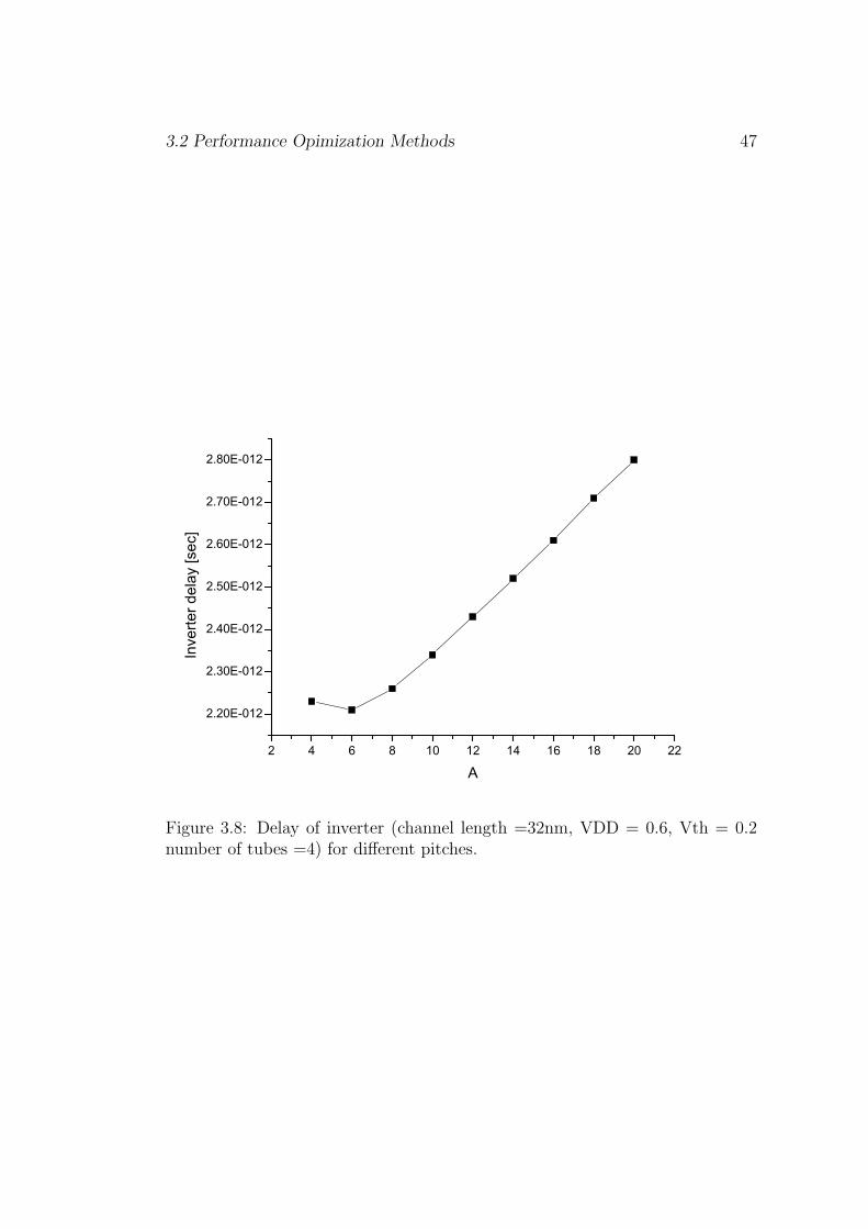
3.2 Performance Opimization Methods 47
2 4 6 8 10 12 14 16 18 20 22
2.20E-012
2.30E-012
2.40E-012
2.50E-012
2.60E-012
2.70E-012
2.80E-012
Inve
rter d
elay
[sec
]
A
Figure 3.8: Delay of inverter (channel length =32nm, VDD = 0.6, Vth = 0.2number of tubes =4) for different pitches.
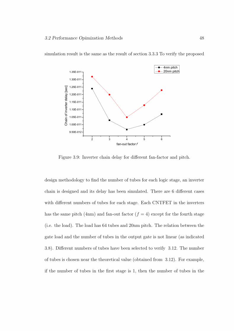
3.2 Performance Opimization Methods 48
simulation result is the same as the result of section 3.3.3 To verify the proposed
2 3 4 5 6
9.50E-012
1.00E-011
1.05E-011
1.10E-011
1.15E-011
1.20E-011
1.25E-011
1.30E-011
1.35E-011
Cha
in o
f inv
erte
r del
ay [s
ec]
fan-out factor f
4nm pitch 20nm pitch
Figure 3.9: Inverter chain delay for different fan-factor and pitch.
design methodology to find the number of tubes for each logic stage, an inverter
chain is designed and its delay has been simulated. There are 6 different cases
with different numbers of tubes for each stage. Each CNTFET in the inverters
has the same pitch (4nm) and fan-out factor (f = 4) except for the fourth stage
(i.e. the load). The load has 64 tubes and 20nm pitch. The relation between the
gate load and the number of tubes in the output gate is not linear (as indicated
3.8). Different numbers of tubes have been selected to verify 3.12. The number
of tubes is chosen near the theoretical value (obtained from 3.12). For example,
if the number of tubes in the first stage is 1, then the number of tubes in the
3.2 Performance Opimization Methods 49
Figure 3.10: Inverter chain delay for 6 cases.
second stage is given by;
N2 = f ·N1 +K(f, η) = 4 · 1 +K(4, 0.6) ≈ 8
Theoretically, the number of tubes for the second stage must be 8. However,
since an approximation was used when deriving 3.12, the exact number of tubes
for the second stages can be different from 8. Simulation was performed for dif-
ferent numbers of tubes near the value of 8 for the second stage to find the
optimum delay. The optimum number of tubes is found in the same way for
the third stage The number of tubes in each stage is denoted as(1st, 2nd, 3d, 4th).
From case 1 to case 6 the numbers of tubes are given by (1,4,16,64), (1,6,24,64),
(1,7,32,64), (1,8,36,64), (1,9,40,64), (1,10,44,64). For Case 1, the screening ef-
fect is not considered. For all cases, the first stage inverter has only one tube
(corresponding to a minimum sized inverter), the number of tube for the second
3.2 Performance Opimization Methods 50
stage (i.e. (4,6,7,8,9,10)) was chosen near the theoretical value (i.e. 8), and the
number of tubes for the third and the fourth inverters are determined based on
3.12.The delay of the inverter chain is shown in Fig 3.10; these results shows
that either case 3 or case 4 provides the best delay and this value is close to the
value obtained from 3.12. Therefore, simulation has shown that the proposed
methodology is effective in finding the optimum number of CNTs for minimum
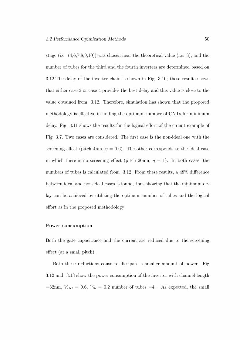
delay. Fig 3.11 shows the results for the logical effort of the circuit example of
Fig 3.7. Two cases are considered. The first case is the non-ideal one with the
screening effect (pitch 4nm, η = 0.6). The other corresponds to the ideal case
in which there is no screening effect (pitch 20nm, η = 1). In both cases, the
numbers of tubes is calculated from 3.12. From these results, a 48% difference
between ideal and non-ideal cases is found, thus showing that the minimum de-
lay can be achieved by utilizing the optimum number of tubes and the logical
effort as in the proposed methodology
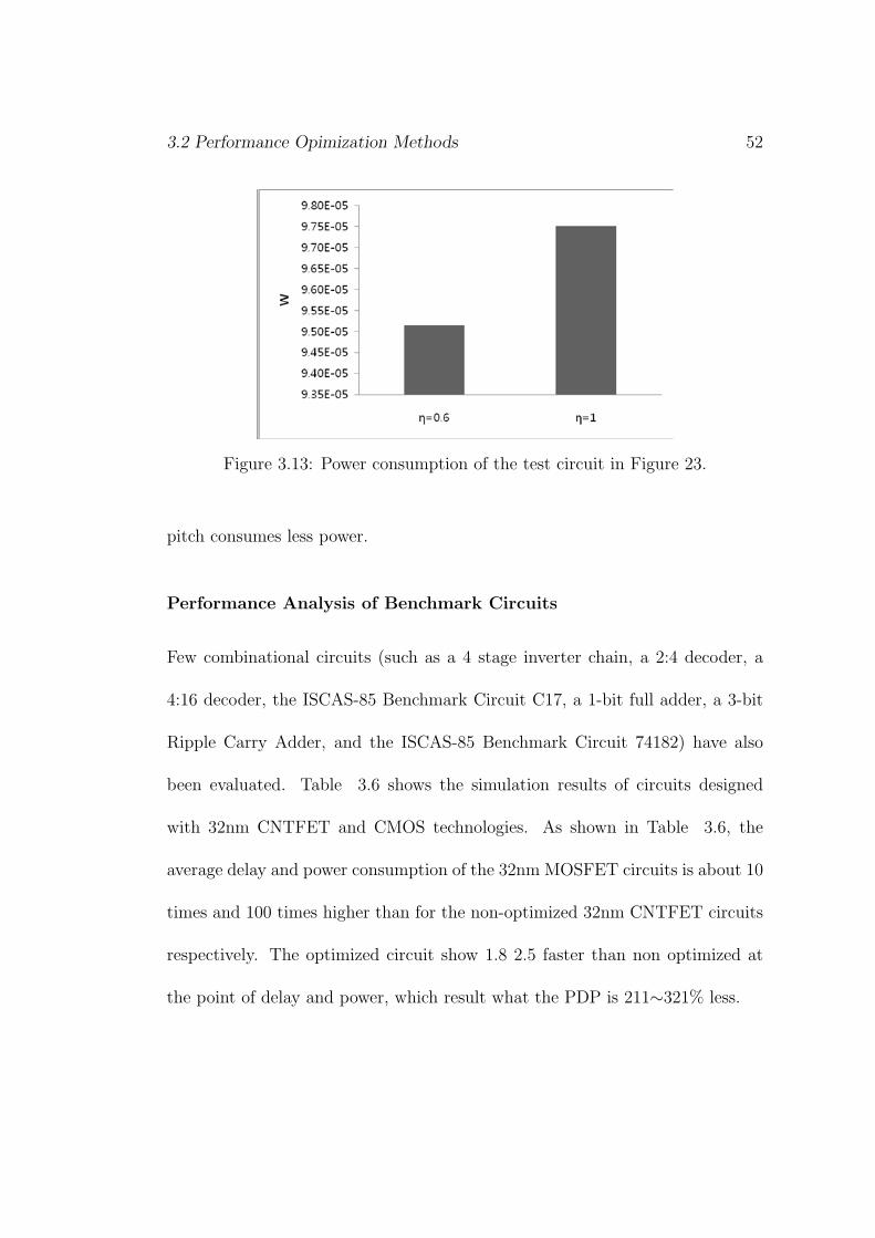
Power consumption
Both the gate capacitance and the current are reduced due to the screening
effect (at a small pitch).
Both these reductions cause to dissipate a smaller amount of power. Fig
3.12 and 3.13 show the power consumption of the inverter with channel length
=32nm, VDD = 0.6, Vth = 0.2 number of tubes =4 . As expected, the small
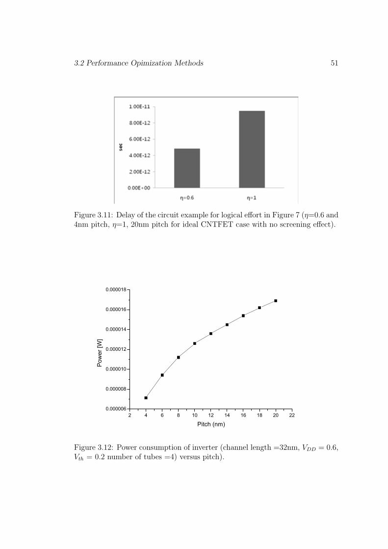
3.2 Performance Opimization Methods 51
Figure 3.11: Delay of the circuit example for logical effort in Figure 7 (η=0.6 and4nm pitch, η=1, 20nm pitch for ideal CNTFET case with no screening effect).
2 4 6 8 10 12 14 16 18 20 220.000006
0.000008
0.000010
0.000012
0.000014
0.000016
0.000018
Pow
er [W
]
Pitch (nm)
Figure 3.12: Power consumption of inverter (channel length =32nm, VDD = 0.6,Vth = 0.2 number of tubes =4) versus pitch).
3.2 Performance Opimization Methods 52
Figure 3.13: Power consumption of the test circuit in Figure 23.
pitch consumes less power.
Performance Analysis of Benchmark Circuits
Few combinational circuits (such as a 4 stage inverter chain, a 2:4 decoder, a
4:16 decoder, the ISCAS-85 Benchmark Circuit C17, a 1-bit full adder, a 3-bit
Ripple Carry Adder, and the ISCAS-85 Benchmark Circuit 74182) have also
been evaluated. Table 3.6 shows the simulation results of circuits designed
with 32nm CNTFET and CMOS technologies. As shown in Table 3.6, the
average delay and power consumption of the 32nm MOSFET circuits is about 10
times and 100 times higher than for the non-optimized 32nm CNTFET circuits
respectively. The optimized circuit show 1.8 2.5 faster than non optimized at
the point of delay and power, which result what the PDP is 211∼321% less.
3.3 Summary 53
Inv 2:4 4:16 C17 1-bit Full 3-bit Ripple 74182Chain Decoder Decoder Adder Carry Adder
Delay(sec) MOSFET 2.89E-11 3.01E-11 5.50E-11 3.81E-11 5.18E-11 8.53E-11 6.40E-11CNFET 4.34E-12 4.97E-12 9.65E-12 6.85E-12 8.10E-12 1.12E-11 7.67E-12
(Non-optimized)CNFET 2.11E-12 2.32E-12 4.76E-12 3.83E-12. 4.21E-12 6.80E-12 4.12E-12
(optimized)Power(W) MOSFET 9.60E-07 7.81E-06 1.03E-05 6.97E-06 9.46E-06 2.53E-05 9.22E-06
CNFET 8.16E-08 7.30E-07 1.22E-06 6.71E-07 9.09E-07 1.30E-06 6.20E-07(Non-optimized)
CNFET 4.42E-08 3.30E-07 6.80E-07 4.31E-07 4.80E-07 6.91E-07 3.70E-07(optimized)
PDP(J) MOSFET 2.77E-17 2.35E-16 5.65E-16 2.66E-16 4.91E-16 2.16E-15 5.90E-16CNFET 3.54E-19 3.62E-18 1.17E-17 4.60E-18 7.36E-18 1.58E-17 4.75E-18
(Non-optimized)CNFET 9.33E-20 7.66E-19 3.24E-18 1.65E-18 2.02E-18 4.70E-18 1.52E+18
(optimized)
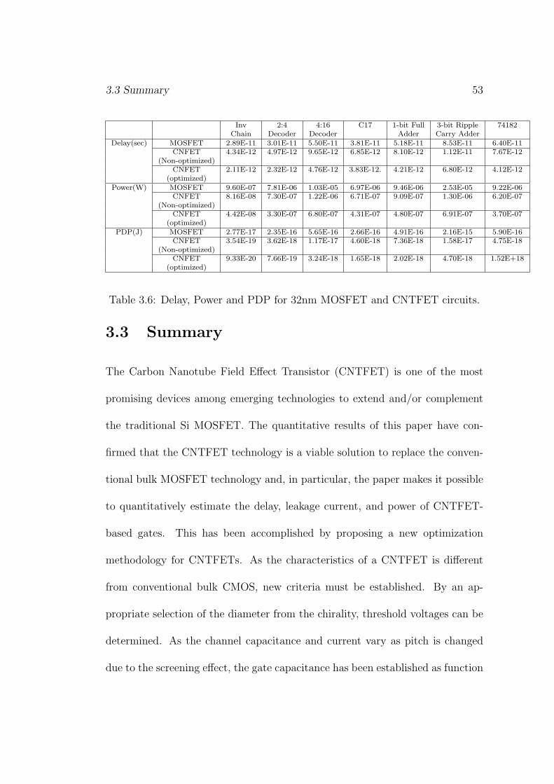
Table 3.6: Delay, Power and PDP for 32nm MOSFET and CNTFET circuits.
3.3 Summary
The Carbon Nanotube Field Effect Transistor (CNTFET) is one of the most
promising devices among emerging technologies to extend and/or complement
the traditional Si MOSFET. The quantitative results of this paper have con-
firmed that the CNTFET technology is a viable solution to replace the conven-
tional bulk MOSFET technology and, in particular, the paper makes it possible
to quantitatively estimate the delay, leakage current, and power of CNTFET-
based gates. This has been accomplished by proposing a new optimization
methodology for CNTFETs. As the characteristics of a CNTFET is different
from conventional bulk CMOS, new criteria must be established. By an ap-
propriate selection of the diameter from the chirality, threshold voltages can be
determined. As the channel capacitance and current vary as pitch is changed
due to the screening effect, the gate capacitance has been established as function

3.3 Summary 54
of the number of tubes in the device and the optimum fan-out factor has been
found. Using these parameter, the logical effort has been calculated and the
minimum delay of a multistage circuit topology has been analyzed. To prove
the effectiveness of the proposed gate-level design method, simulation has been
performed using HSPICE with the CNTFET library of [22], Results have demon-
strated that the proposed design methodology is both effective and practical .
To design a CNFET circuit, many parameters must be considered, among them
the diameter at certain chirality, pitch and the optimum number of tubes have
been shown to be of primary importance.
Chapter 4
Low Power SRAM Design using
CNFET
4.1 Introduction
In this Chapter, a new SRAM cell design based on Carbon Nanotube Field-
Effect Transistor (CNFET) technology is proposed. The proposed SRAM cell
design for CNFET is compared with SRAM cell designs implemented with the
conventional CMOS and FinFET in terms of speed, power consumption, stabil-
ity, and leakage current. The HSPICE simulation and analysis show that the
dynamic power consumption of the proposed 8T CNFET SRAM cell’s is reduced
about 48% and the SNM is widened up to 56% compared to the conventional
CMOS SRAM structure at the expense of 2% leakage power and 3% write delay
4.1 Introduction 56
increase.
An estimated 70% of the transistors in a billion-transistor superscalar micro-
processor are expected to be used for memory arrays, especially for large L2 and
L3 SRAM data caches. Therefore, it is essential to develop a low power SRAM
design technique for the new device technology such as CNFET.
In this paper, as a circuit level design of CNFET, a novel low power 8T SRAM
cell design is proposed and its performance and viability are demonstrated by
performing various simulations. The performance, power consumption, stabil-
ity, and leakage currents of the 6T and 8T SRAM cell based on CNFET are
compared with those of the conventional CMOS and FinFET based SRAM cell
designs to show the viability of the CNFET based SRAM cell design.
In section II, the characteristics and physical features of CNFET are ex-
plained, and the mechanisms of the read and write operations of the proposed
8T CNFET SRAM cell are explained and the schemes for deciding the number
of nanotubes of each CNFET are described in section III. In section IV, the sim-
ulation results are presented to compare the performance and viability of the
CNFET technology with those of other technologies, followed by the conclusion
in Section V.

4.2 Low power 8T SRAM Cell 57
4.2 Low power 8T SRAM Cell
4.2.1 Write/Read operations
In the proposed 8T SRAM, the write and read bits are separated. While bit
and bit-bar lines are used for writing data in the traditional 6T SRAM, only the
WRITE BIT in Figure 2 is used in the proposed SRAM cell to write for both
”0” and ”1” data. The writing operation starts by disconnecting the feedback
loop of the two inverters. By setting ’W bar’ signal to ”0”, the feedback loop
is disconnected. The data that is going to be written is determined by the
WRITE BIT voltage. If the feedback connection is disconnected, SRAM cell
has just two cascaded inverters. WRITE BIT transfers the complementary of
the input data to Q2, cell data, which drives the other inverter (P2 and N2)
to develop Q bar. WRITE BIT have to be pre-charged ”high” before and right
after each write operation. When writing ”0” data, negligible writing power is
consumed because there is no discharging activity at WRITE BIT. To write ’1’
data at Q2,
The WRITE BIT have to be discharged to ground level, just like 6T SRAM
cell. In this case, the dynamic power consumed by the discharging is the same
as 6T SRAM. The write circuit does not discharge for every write operation
but discharges only when the cell writes ”1” data, and the activity factor of the
discharging WRITE BIT is less than ”1”, which makes the proposed SRAM cell

4.2 Low power 8T SRAM Cell 58
more power effective during writing operation compared with the conventional
ones.
All the Read Bit lines are pre-charged before any READ operation. During
read operation, transistor N5 is turned on by setting W bar signal high and the
READ ROW(RD) is ”high” to turn on N6. When Q2=”0”, the N4 is off making
the READ BIT voltage not change from the pre-charged value, which means the
cell data Q2 holds ”0”. On the other hand, If Q2= ”1”, the transistors N4 and
N6 are turned on. In this case, due to charge sharing, the READ BIT voltage
will be dropped about 100 200mV, which is enough to be detected in the sense
amplifier.
4.2.2 Carbon nanotube configuration
The operation of writing ”1” is stable because NMOS transistor N3 can pass ”0”
faithfully. On the other hand, when writing ”0”, WRITE BIT is pre-charged
high (VDD) and N5 is turned off. The node voltage at Q1 is less than VDD due
to the threshold voltage drop between the gate and source of the transistor N3.
To compensate this voltage drop, the transistor N2 and P2 must be designed
as a low-skew inverter to ensure Q2 to be solid ground level to represent ”0”
state. A low-skewed inverter has a weaker PMOS transistor. If the PMOS
CNFET have only one tube, the current is minimum. Let’s suppose that the
cell stores ”0” at Q2 and ”1” at Q bar after WL(Word Line) is deactivated and
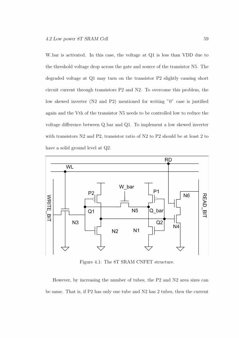
4.2 Low power 8T SRAM Cell 59
W bar is activated. In this case, the voltage at Q1 is less than VDD due to
the threshold voltage drop across the gate and source of the transistor N5. The
degraded voltage at Q1 may turn on the transistor P2 slightly causing short
circuit current through transistors P2 and N2. To overcome this problem, the
low skewed inverter (N2 and P2) mentioned for writing ”0” case is justified
again and the Vth of the transistor N5 needs to be controlled low to reduce the
voltage difference between Q bar and Q1. To implement a low skewed inverter
with transistors N2 and P2, transistor ratio of N2 to P2 should be at least 2 to
have a solid ground level at Q2.
Figure 4.1: The 8T SRAM CNFET structure.
However, by increasing the number of tubes, the P2 and N2 area sizes can
be same. That is, if P2 has only one tube and N2 has 2 tubes, then the current
4.3 SIMULATION RESULTS 60
ratio N2/P2 can be more than 2. This means that the inverter transistor sizes
N2/P2 can be smaller than 2 by controlling the number of tubes. Transistor
ratio N3/P2 of 1.3, N1/P2 of 3, and low Vth of the transistor N5 guarantees a
stable READ operation when Q bar stores ”0”. However, if the similar approach
to N2/P2 sizing is used to optimize transistor ratios among N1, N3 and P2, the
transistor sizes can be further reduced. If N3 has only one tube, N1 has two tubes
and P2 has one tube, the transistor N1 needs to be only 1.5 times larger than
transistor P2 to satisfy the relationships among N1, N3, and P2. Combining the
threshold voltage controllabilityF of the CNFET varying the diameter of tubes
and transistor sizing techniques, the proposed 8T SRAM cell can accomplish
low power consumption due to smaller node capacitance and tuning Vth at the
minimal cost of the area overhead.
4.3 SIMULATION RESULTS
In order to compare performances, total 8 different SRAM cells are designed;
Each 6T SRAM and 8T SRAM cells are designed using tied FinFETS (front and
back gates of the FinFETS are tied together), independent double gates Fin-
FETS(front and back gates are independently controlled), CMOS and CNFET.
The 6T independent gate FinFET SRAM (6T-Ind) is implemented by using in-
dependent gate control which connects the back gates of the NMOS (PMOS)
transistors to GND (VDD) to reduce the leakage current . An independent-gate
4.3 SIMULATION RESULTS 61
FinFET operates in the dual-gate mode (DGM) when both gates are biased
to induce channel inversion. Alternatively, an independent-gate n-FinFET (p-
FinFET) operates in the single-gate mode when one of the gates is deactivated
by connecting the gate to ground (VDD). Disabling one of the gates in the
single-gate mode (SGM) increases the absolute value of the threshold voltage
compared to DGM. Therefore, it is possible to modulate the threshold voltage
of the FinFET by biasing the two gates independently [36]. And the proposed
8T SRAM (8T-Ind) configuration is that back gate of PMOS connected to the
VDD and front and back gates of N1, N2, N6 are tied together and back gate
of N3, N4 are connected together.
4.3.1 Simulation setup
The technology parameters for the FinFETs are; channel length (L) = 32nm,
fin height (Hfin) = 32nm, fin thickness (tsi) = 8nm, oxide thickness(tox) =
1.6nm, channel doping = 2 x 1020 cm-3 ,source/ drain doping = 2 x 1020 cm-3,
work functions (N-FinFET) = 4.5eV , work functions (P-FinFET) = 4.9eV. The
technology parameters for the CNFETs are : physical channel length = 32.0nm,
10nm (this value used in simulations for performances with VDD variations),
the length of doped CNT drain-side/source-side extension region = 32.0nm ,
fermi level of the doped S/D tube. = 0.6 eV, the thickness of high-k top gate
dielectric material = 4.0nm, chirality of tube = (19,0), Pitch = 10nm, Vfbn,
4.3 SIMULATION RESULTS 62
Vfbp (flatband voltage for n-CNFET and p-CNFET) = 0.0eV, 0.0eV , physical
gate length = 32.0nm, The mean free path in intrinsic CNT = 200.0nm, the
length of doped CNT source/drain extension region. = 32.0nm, the mean free
path in p+/n+ doped CNT = 15.0nm, the work function of Source/Drain metal
contact = 4.6eV, CNT work function = 4.5eV. The minimum transistor sizes
used for those technologies are W=48nm and L = 32nm for bulk CMOS, Hfin
=32nm and L = 32nm for FinFET, and L=32nm and the number of tubes =1
for CNFET. The HSPICE using the Predictive Technology Model (PTM) model
and Stanford University CNFET model is used to simulate the performance of
the proposed 8T SRAM and the conventional 6T SRAM cells designed with
CMOS, FinFET, and CNFET transistors.
4.3.2 Dynamic power consumption
The proposed 8T SRAM achieves 48% writing power saving while maintaining
the cell performance, read/write delay, and stability of the conventional cell.
The power saving comes from the fact that the cell keeps WRITE BIT ”high”
instead of discharging when it writes ”0”, which reduces the activity factor of
the WRITE BIT.
While conventional 6T SRAM always discharges one of the bit lines to write a
data into the cell, the proposed 8T SRAM discharge the WRITE BIT only when
it writes ”1”. As the probability of writing ’0’ gets higher, the power dissipation
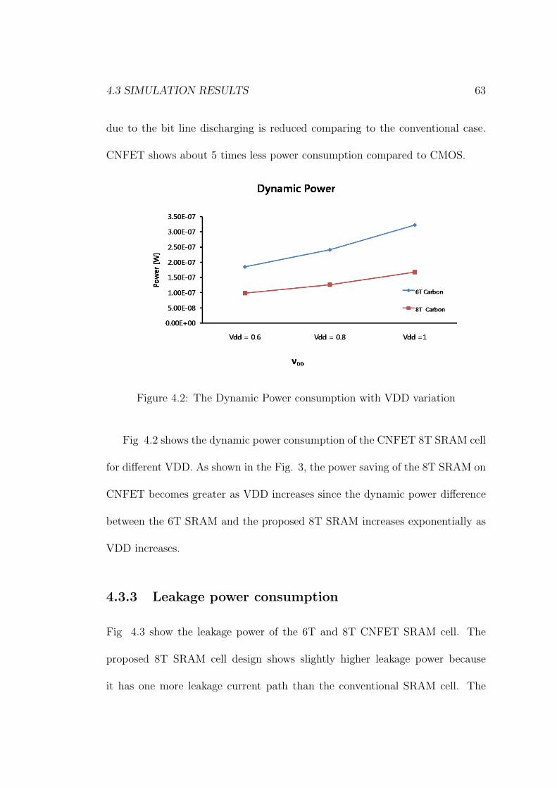
4.3 SIMULATION RESULTS 63
due to the bit line discharging is reduced comparing to the conventional case.
CNFET shows about 5 times less power consumption compared to CMOS.
Figure 4.2: The Dynamic Power consumption with VDD variation
Fig 4.2 shows the dynamic power consumption of the CNFET 8T SRAM cell
for different VDD. As shown in the Fig. 3, the power saving of the 8T SRAM on
CNFET becomes greater as VDD increases since the dynamic power difference
between the 6T SRAM and the proposed 8T SRAM increases exponentially as
VDD increases.
4.3.3 Leakage power consumption
Fig 4.3 show the leakage power of the 6T and 8T CNFET SRAM cell. The
proposed 8T SRAM cell design shows slightly higher leakage power because
it has one more leakage current path than the conventional SRAM cell. The
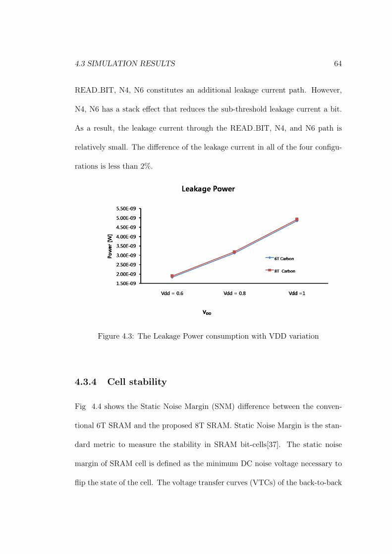
4.3 SIMULATION RESULTS 64
READ BIT, N4, N6 constitutes an additional leakage current path. However,
N4, N6 has a stack effect that reduces the sub-threshold leakage current a bit.
As a result, the leakage current through the READ BIT, N4, and N6 path is
relatively small. The difference of the leakage current in all of the four configu-
rations is less than 2%.
Figure 4.3: The Leakage Power consumption with VDD variation
4.3.4 Cell stability
Fig 4.4 shows the Static Noise Margin (SNM) difference between the conven-
tional 6T SRAM and the proposed 8T SRAM. Static Noise Margin is the stan-
dard metric to measure the stability in SRAM bit-cells[37]. The static noise
margin of SRAM cell is defined as the minimum DC noise voltage necessary to
flip the state of the cell. The voltage transfer curves (VTCs) of the back-to-back
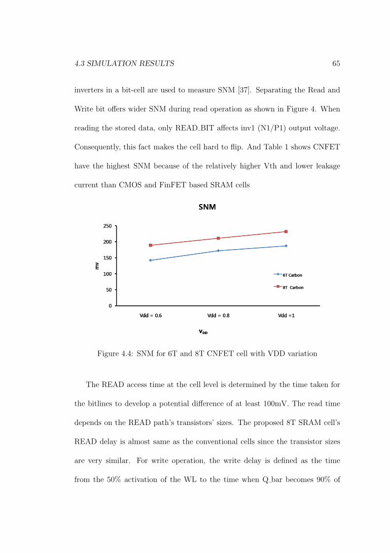
4.3 SIMULATION RESULTS 65
inverters in a bit-cell are used to measure SNM [37]. Separating the Read and
Write bit offers wider SNM during read operation as shown in Figure 4. When
reading the stored data, only READ BIT affects inv1 (N1/P1) output voltage.
Consequently, this fact makes the cell hard to flip. And Table 1 shows CNFET
have the highest SNM because of the relatively higher Vth and lower leakage
current than CMOS and FinFET based SRAM cells
Figure 4.4: SNM for 6T and 8T CNFET cell with VDD variation
The READ access time at the cell level is determined by the time taken for
the bitlines to develop a potential difference of at least 100mV. The read time
depends on the READ path’s transistors’ sizes. The proposed 8T SRAM cell’s
READ delay is almost same as the conventional cells since the transistor sizes
are very similar. For write operation, the write delay is defined as the time
from the 50% activation of the WL to the time when Q bar becomes 90% of
4.4 Summary 66
its full swing. The write delay is approximately equal to the propagation delay
of the inv2 (N2/P2) and inv1. Because the inv1 is only driving the diffusion
capacitor of N5, it is desirable to reduce the input capacitance of the inv1 as
much as possible to reduce the load capacitance on inv2. The proposed 8T
SRAM is slightly slower than 6T SRAM in writing operation because of this
reason. Because the device performance based on intrinsic CV/I gate delay
metric [22] is 6 time for nFET and 14 times for pFET higher than CMOS, the
speed of the write and read operation in CNFET is about 5 or 6 times faster
than CMOS and FinFET technologies.
4.4 Summary
The new SRAM cell cuts off the feedback connection between the two back-to-
back inverters in the SRAM cell when data is written and separates the write and
read port with 8 transistors. The proposed technique saves dynamic power by
reducing discharging frequency during write operation. Compared to 6T SRAM
structure, the proposed 8T SRAM saves power up to 48% and obtains 56% wider
SNM during read operation at the minimal cost of 2% leakage power and 3%
delay increase. As the cells are more frequently accessed, the dynamic power
saving is linearly increased. This paper also compares CMOS, FinFET and CNT
6T and 8T SRAM cells using HSPICE simulations. The result demonstrates
from 3 to 7 times less dynamic power consumption, from 11 to17 times less

4.4 Summary 67
leakage power consumption, from 5 to 6 times faster read and write operations,
and 1.6 wider SNM than the conventional designs.
Chapter 5
High Speed and Low Power
Transceiver Design for CNFET
and CNT Interconnect
5.1 Introduction
On-chip communication has become an active research area in the past few years.
This not only because on-chip interconnects are becoming a speed, power, and
reliability bottleneck [38], but also because systems on chips (SoCs) start to
become so complex that they require new interconnection approaches [39], [40].
Therefore, high-speed, low power wire-line communication has been required
5.1 Introduction 69
by the modern computer systems, and the demand for more sophisticated in-
put/output (I/O) transceiver design has been increased accordingly.
However, the environment of the communication channel and the semicon-
ductor technology (transistor size, material and wire material) limit the max-
imum symbol rate of the serial data transmission and power is consumed by
data transmission. Therefore, many researches have been done to save power
and increase the data rate while keeping the same symbol rate and sustaining
the signal integrity. Among them, increasing the data rate methods are the
pulse-amplitude modulation (PAM) [41] , pulse-width modulation (PWM) [42]
and using carbon nano tube (CNT) bundle [45] by reducing wire capacitance.
[40] introduced a transceiver that uses both PWM and PAM modulation for the
first time to boost the data transmission rate. However, its application is limited
to a relatively low-speed data transmission (250M symbol/s) and it utilizes the
conventional PWM and PAM symbol representations . It also needs complex
circuit components for PWM, PAM modulation and demodulation. Due to the
switched capacitances of interconnect, on-chip wires also present an increasing
energy problem. A CMOS wire driver running at an effective frequency must
switch a total wire capacitance Cw through the voltage, leading to a power cost
proportional to CV 2f . Under technology scaling Cw, remains largely constant,
voltage scales down slowly, and frequency (f) scales up while leading to nearly
constant power per wire. However, as chip’s device integration level increases
5.1 Introduction 70
continuously, this constant power per wire gets multiplied by an ever-increasing
number of wires. In order to save power consumption which is caused by wires,
Cw and V 2 have to be reduced. These can be realized by using low swing voltage
as a wire symbol signal and changing wire material with CNT bundle. Circuits
using optimized low-voltage swings as a wire signal have shown 10 times energy
savings[4] because reducing voltage level save the power which is proportional to
CV 2f. But such low-swing systems typically require an expensive second power
supply, which breaks up power distribution planes on the chip and in the pack-
age requiring additional voltage regulator modules at low target impedances.
To overcome these drawback of the low swing techniques, a coupling capaci-
tor in line with the long wire which pre-emphasizes transitions is proposed in
[46][47] to reduce wire delay and to reduce the load seen by the driver. It also
lowers the wire’s voltage swing without additional power supply. A number
of on-chip transceiver improvements have been proposed in the past, but they
usually reduce either the power consumed in the interconnect [48], [49] or im-
prove the data-rate achievable over the interconnect [50],[51]. In this paper , the
proposed transceiver will adapted PWAM modulation techniques and capacitive
transmitting scheme to achieve high data rate and save power with relatively
simple modulation circuit and only one power supply voltage. Furthermore, the
proposed transceiver is implemented with CNFET and CNT bundle technolo-
gies and it will show superior performance compared to CMOS and Cu wire.
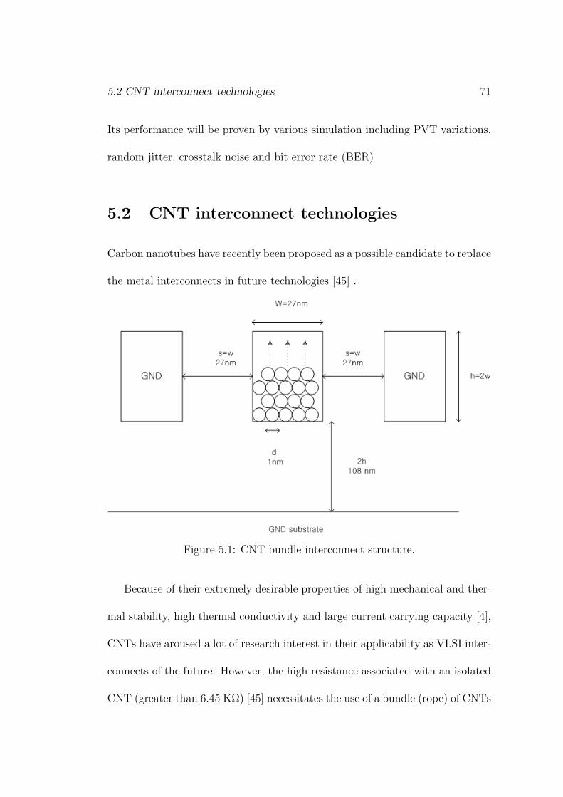
5.2 CNT interconnect technologies 71
Its performance will be proven by various simulation including PVT variations,
random jitter, crosstalk noise and bit error rate (BER)
5.2 CNT interconnect technologies
Carbon nanotubes have recently been proposed as a possible candidate to replace
the metal interconnects in future technologies [45] .
Figure 5.1: CNT bundle interconnect structure.
Because of their extremely desirable properties of high mechanical and ther-
mal stability, high thermal conductivity and large current carrying capacity [4],
CNTs have aroused a lot of research interest in their applicability as VLSI inter-
connects of the future. However, the high resistance associated with an isolated
CNT (greater than 6.45 KΩ) [45] necessitates the use of a bundle (rope) of CNTs

5.3 PWAM SCHEME 72
conducting current in parallel to form an interconnection [21] as shown in Fig.
5.2. Moreover, due to the lack of control on chirality, any bundle of CNTs con-
sists of metallic as well as semi-conducting nanotubes. CNTs are also classified
into single-walled and multi-walled nanotubes. Single-walled CNTs (SWCNTs)
have electron mean free paths of the order of a micron [45]. Therefore, in the
domain of interconnects, metallic SWCNTs are the preferred candidates, and
the single-walled metallic CNT bundle structure is used for the channel media
between the transmitter and receiver in this paper Noise and bit error rate of
the transceiver is estimated and analyzed based on the interconnect structure.
5.3 PWAM SCHEME
PWAM-(MxN) scheme combines PAM-M (M is the number of different voltage
levels) and PWM-N (N is the number of different pulse widths) together. With
M different pulse amplitudes and N different pulse widths, there exist M×N dif-
ferent symbol representations. M×N symbols represent log2M+log2N bit binary
information. Therefore, the bit rate of PWAM-(M×N) is log2M +log2N times
the symbol rate. PWAM-(4×4) is illustrated in Fig 5.2(c) as an example to show
the symbol representations of PWAM. One PWAM-(4×4) symbol denotes 4-bit
data. The 4-bit data have 16 different values, thus 16 PWAM-(4×4) symbols
are used to stand for 16 different values (hereafter, 4-bit data are represented
by hex 0, 1, ....a, b, c, d, e, f). These 16 symbols are divided into four groups
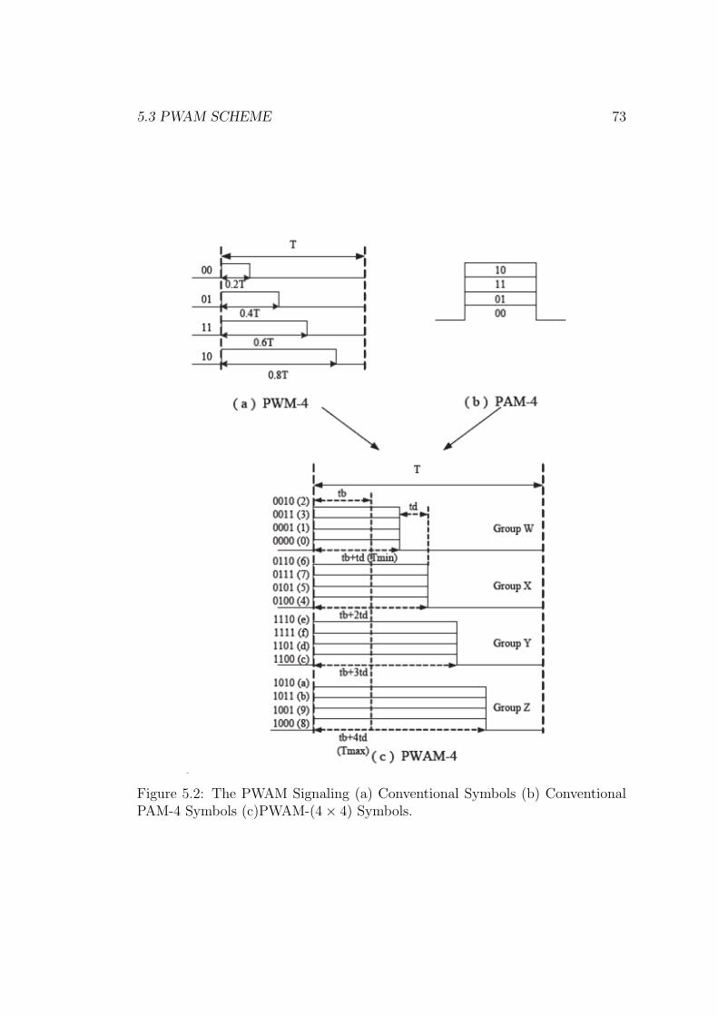
5.3 PWAM SCHEME 73
Figure 5.2: The PWAM Signaling (a) Conventional Symbols (b) ConventionalPAM-4 Symbols (c)PWAM-(4× 4) Symbols.
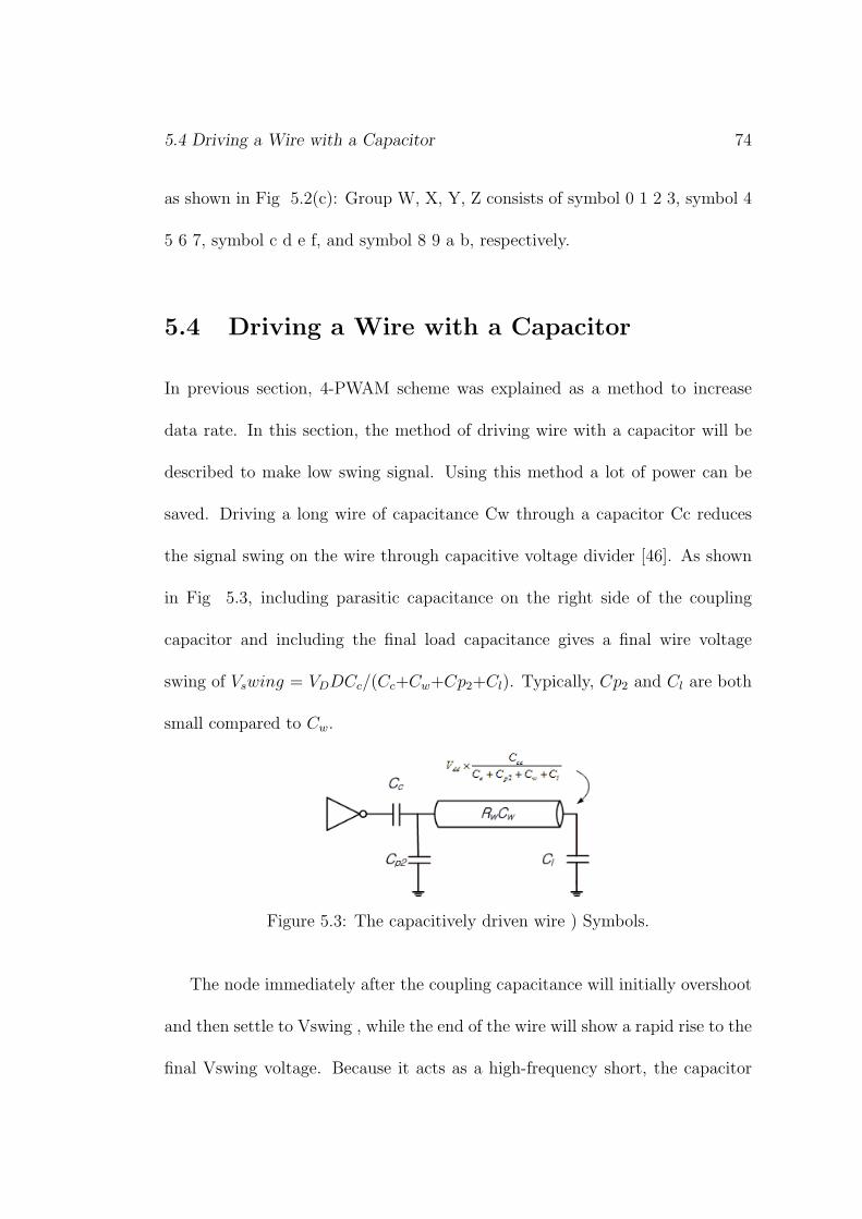
5.4 Driving a Wire with a Capacitor 74
as shown in Fig 5.2(c): Group W, X, Y, Z consists of symbol 0 1 2 3, symbol 4
5 6 7, symbol c d e f, and symbol 8 9 a b, respectively.
5.4 Driving a Wire with a Capacitor
In previous section, 4-PWAM scheme was explained as a method to increase
data rate. In this section, the method of driving wire with a capacitor will be
described to make low swing signal. Using this method a lot of power can be
saved. Driving a long wire of capacitance Cw through a capacitor Cc reduces
the signal swing on the wire through capacitive voltage divider [46]. As shown
in Fig 5.3, including parasitic capacitance on the right side of the coupling
capacitor and including the final load capacitance gives a final wire voltage
swing of Vswing = VDDCc/(Cc+Cw+Cp2+Cl). Typically, Cp2 and Cl are both
small compared to Cw.
Figure 5.3: The capacitively driven wire ) Symbols.
The node immediately after the coupling capacitance will initially overshoot
and then settle to Vswing , while the end of the wire will show a rapid rise to the
final Vswing voltage. Because it acts as a high-frequency short, the capacitor

5.5 Energy Consumption Of Transceiver 75
increases the 3-dB bandwidth of the long wire, allowing shorter cycle times and
decreasing latency. Long wires have a low-pass frequency response that limits
their operating speed. Capacitive coupling to a long wire creates a pole-zero
pair, giving high-frequency emphasis that mitigates the low-pass wire response
and increases performance.
Therefore, the capacitive transmitter increases the bandwidth of the inter-
connect, as it emphasizes each transition with an overshoot. Compared to the
low-swing transmitters that switch between supplies, the capacitive transmitter
also is much less sensitive to supply noise, as the capacitor divider also attenuates
this noise.
5.5 Energy Consumption Of Transceiver
The energy-cost for a rising edge with swing V equals the well-known E=CV 2 .
Half of this energy is dissipated during charging. The other half is stored in the
interconnect and dissipated at a later time when the interconnect is discharged
(the resistance of the interconnect prevents efficient charge-recycling techniques).
Therefore, to reduce the link power, it is necessary to reduce the swing. If
only a single supply voltage is available and active circuits are used to reduce
the swing, there is no quadratic but linearly relation with the swing. When a
dedicated supply voltage is available to generate the low-swing signal, then the
power is again quadratically dependent on the swing. Therefore, using dedicated
5.6 4-PWAM Circuit Design 76
supply voltage is effect to generate low swing signal as a result, many low-swing
techniques with a dedicated supply voltage (either generated on- or off-chip) for
the transmitter have been introduced in the past [48],[49],[46], [52].
However, in this work the capacitive transmitter uses a series capacitance
(Cc) to drive the interconnect with only single supply voltage. It also lowers the
energy consumption by using a simple structure at the driver circuits .
5.6 4-PWAM Circuit Design
In this section block diagram and circuits of the proposed 4-PWAM transceiver
will be described. In the transmitter circuits, the phase controller circuit , PWM
modulation circuit and adaptive capacitor circuit are proposed and the receiver
circuits are also newly designed
5.6.1 Transmitter circuit
The PWAM transmitter is shown in detail in Fig 5.4. It contains three main
building blocks: a PWM modulator, a PAM modulator, and 8 phase PLL. An
8 Phase PLL provides evenly spaced clock phases that are used to produce
PWM-encoded signals. After processing Tx-bit0 and Tx-bit1 using the PWM
technique, PAM signaling is used to modulate the information from Tx-bit2
and Tx-bit3. In addition to the PWAM modulator, In addition to the PWAM
modulator, capacitively driven wire act as a pre-emphasis block. Pre-emphasis
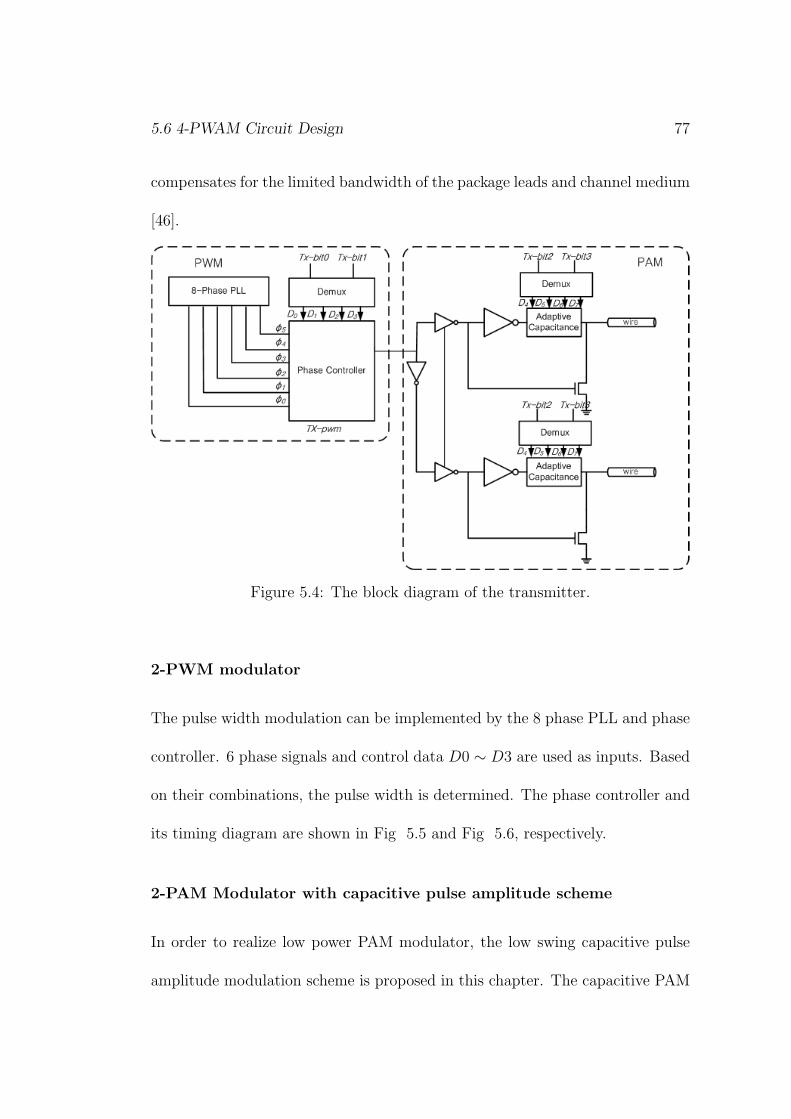
5.6 4-PWAM Circuit Design 77
compensates for the limited bandwidth of the package leads and channel medium
[46].
Figure 5.4: The block diagram of the transmitter.
2-PWM modulator
The pulse width modulation can be implemented by the 8 phase PLL and phase
controller. 6 phase signals and control data D0 ∼ D3 are used as inputs. Based
on their combinations, the pulse width is determined. The phase controller and
its timing diagram are shown in Fig 5.5 and Fig 5.6, respectively.
2-PAM Modulator with capacitive pulse amplitude scheme
In order to realize low power PAM modulator, the low swing capacitive pulse
amplitude modulation scheme is proposed in this chapter. The capacitive PAM
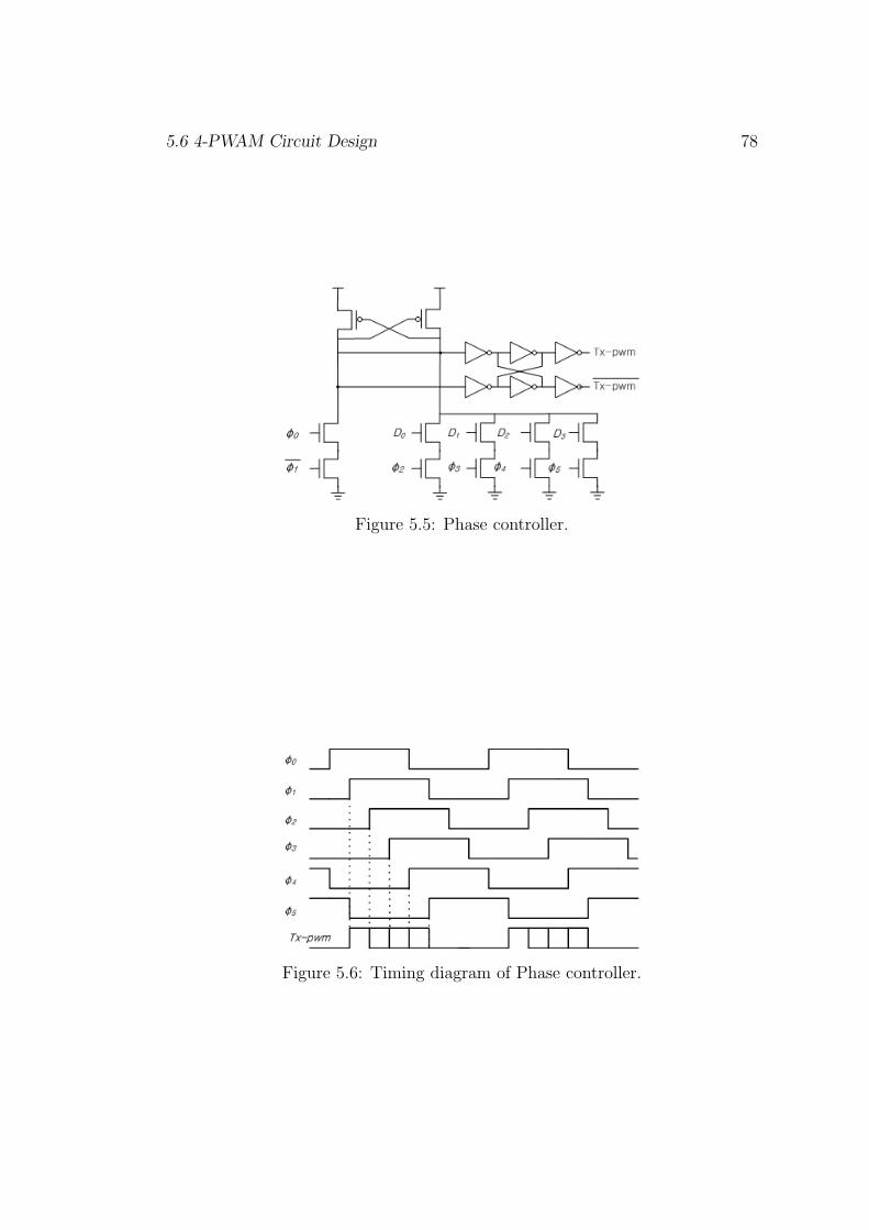
5.6 4-PWAM Circuit Design 78
Figure 5.5: Phase controller.
Figure 5.6: Timing diagram of Phase controller.
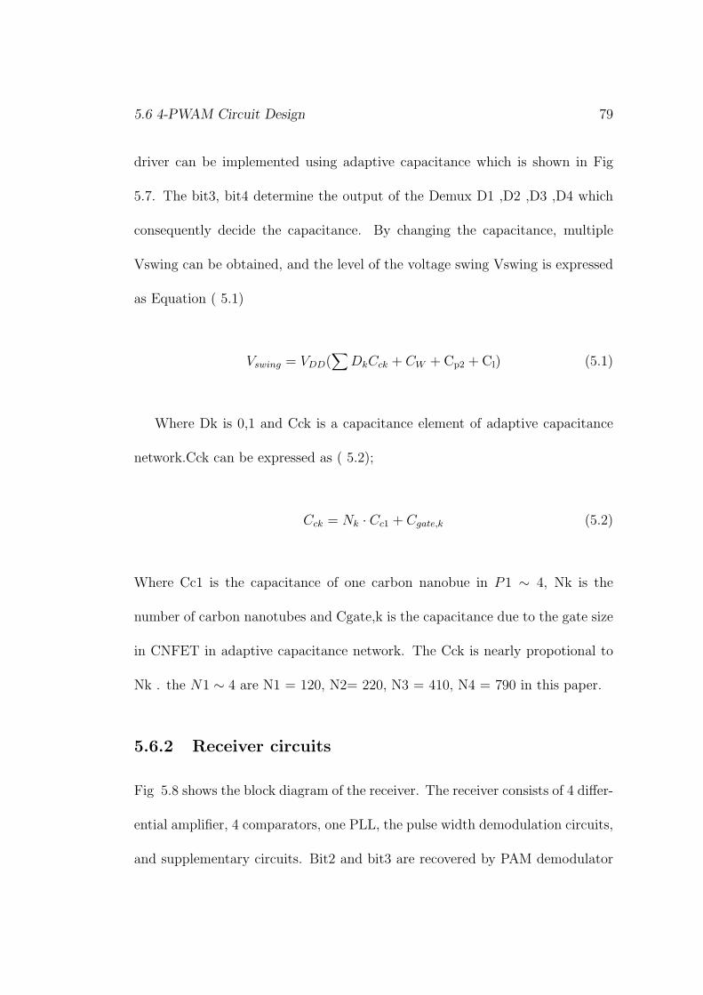
5.6 4-PWAM Circuit Design 79
driver can be implemented using adaptive capacitance which is shown in Fig
5.7. The bit3, bit4 determine the output of the Demux D1 ,D2 ,D3 ,D4 which
consequently decide the capacitance. By changing the capacitance, multiple
Vswing can be obtained, and the level of the voltage swing Vswing is expressed
as Equation ( 5.1)
Vswing = VDD(∑
DkCck + CW + Cp2 + Cl) (5.1)
Where Dk is 0,1 and Cck is a capacitance element of adaptive capacitance
network.Cck can be expressed as ( 5.2);
Cck = Nk · Cc1 + Cgate,k (5.2)
Where Cc1 is the capacitance of one carbon nanobue in P1 ∼ 4, Nk is the
number of carbon nanotubes and Cgate,k is the capacitance due to the gate size
in CNFET in adaptive capacitance network. The Cck is nearly propotional to
Nk . the N1 ∼ 4 are N1 = 120, N2= 220, N3 = 410, N4 = 790 in this paper.
5.6.2 Receiver circuits
Fig 5.8 shows the block diagram of the receiver. The receiver consists of 4 differ-
ential amplifier, 4 comparators, one PLL, the pulse width demodulation circuits,
and supplementary circuits. Bit2 and bit3 are recovered by PAM demodulator
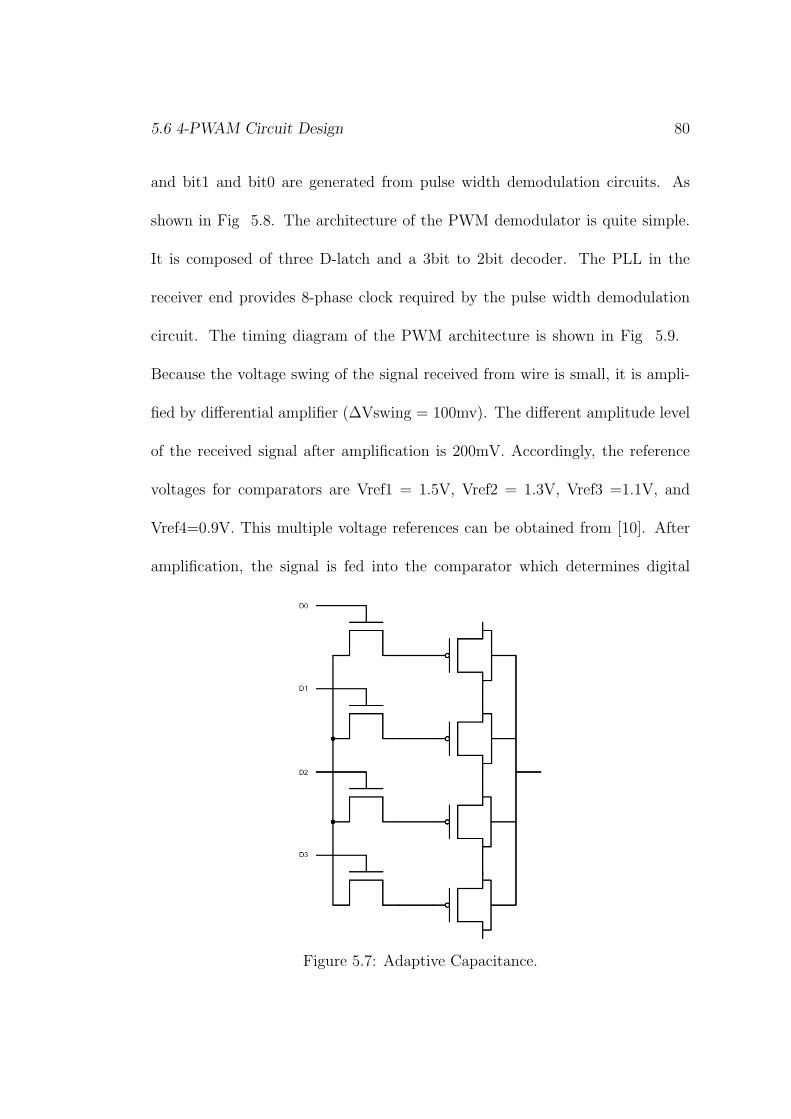
5.6 4-PWAM Circuit Design 80
and bit1 and bit0 are generated from pulse width demodulation circuits. As
shown in Fig 5.8. The architecture of the PWM demodulator is quite simple.
It is composed of three D-latch and a 3bit to 2bit decoder. The PLL in the
receiver end provides 8-phase clock required by the pulse width demodulation
circuit. The timing diagram of the PWM architecture is shown in Fig 5.9.
Because the voltage swing of the signal received from wire is small, it is ampli-
fied by differential amplifier (∆Vswing = 100mv). The different amplitude level
of the received signal after amplification is 200mV. Accordingly, the reference
voltages for comparators are Vref1 = 1.5V, Vref2 = 1.3V, Vref3 =1.1V, and
Vref4=0.9V. This multiple voltage references can be obtained from [10]. After
amplification, the signal is fed into the comparator which determines digital
Figure 5.7: Adaptive Capacitance.
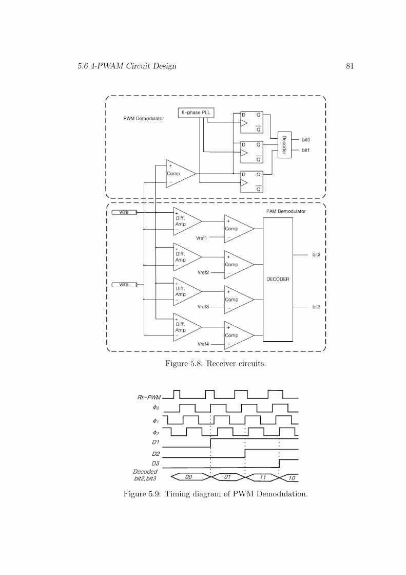
5.6 4-PWAM Circuit Design 81
Figure 5.8: Receiver circuits.
Figure 5.9: Timing diagram of PWM Demodulation.
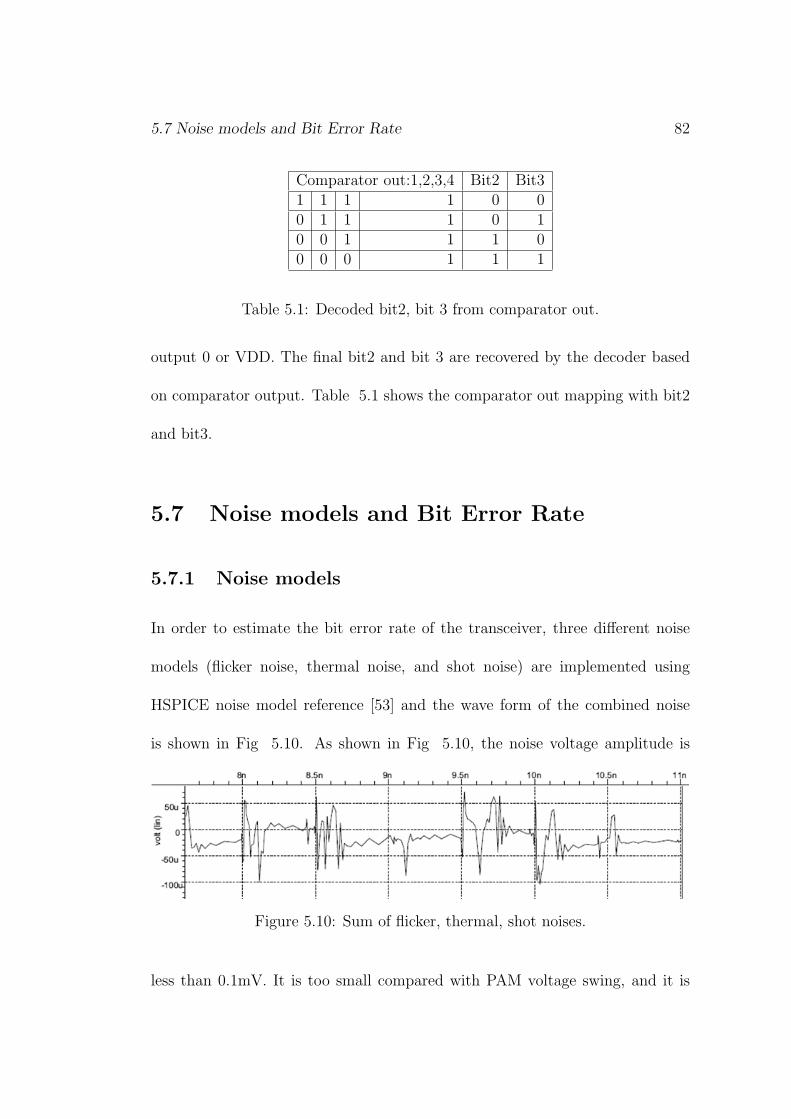
5.7 Noise models and Bit Error Rate 82
Comparator out:1,2,3,4 Bit2 Bit31 1 1 1 0 00 1 1 1 0 10 0 1 1 1 00 0 0 1 1 1
Table 5.1: Decoded bit2, bit 3 from comparator out.
output 0 or VDD. The final bit2 and bit 3 are recovered by the decoder based
on comparator output. Table 5.1 shows the comparator out mapping with bit2
and bit3.
5.7 Noise models and Bit Error Rate
5.7.1 Noise models
In order to estimate the bit error rate of the transceiver, three different noise
models (flicker noise, thermal noise, and shot noise) are implemented using
HSPICE noise model reference [53] and the wave form of the combined noise
is shown in Fig 5.10. As shown in Fig 5.10, the noise voltage amplitude is
Figure 5.10: Sum of flicker, thermal, shot noises.
less than 0.1mV. It is too small compared with PAM voltage swing, and it is
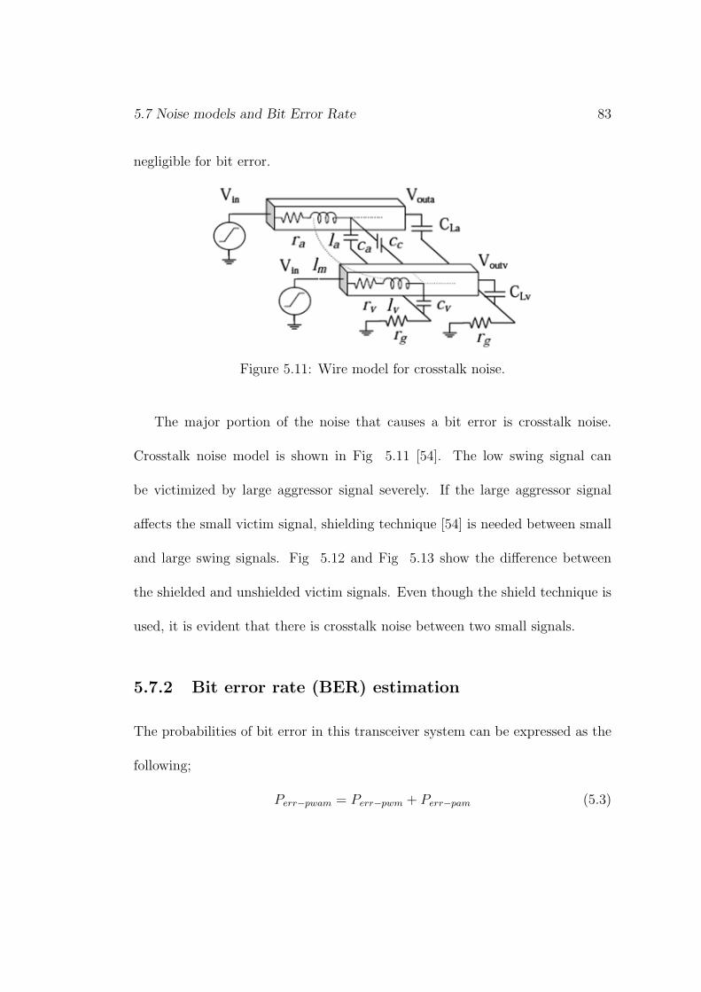
5.7 Noise models and Bit Error Rate 83
negligible for bit error.
Figure 5.11: Wire model for crosstalk noise.
The major portion of the noise that causes a bit error is crosstalk noise.
Crosstalk noise model is shown in Fig 5.11 [54]. The low swing signal can
be victimized by large aggressor signal severely. If the large aggressor signal
affects the small victim signal, shielding technique [54] is needed between small
and large swing signals. Fig 5.12 and Fig 5.13 show the difference between
the shielded and unshielded victim signals. Even though the shield technique is
used, it is evident that there is crosstalk noise between two small signals.
5.7.2 Bit error rate (BER) estimation
The probabilities of bit error in this transceiver system can be expressed as the
following;
Perr−pwam = Perr−pwm + Perr−pam (5.3)
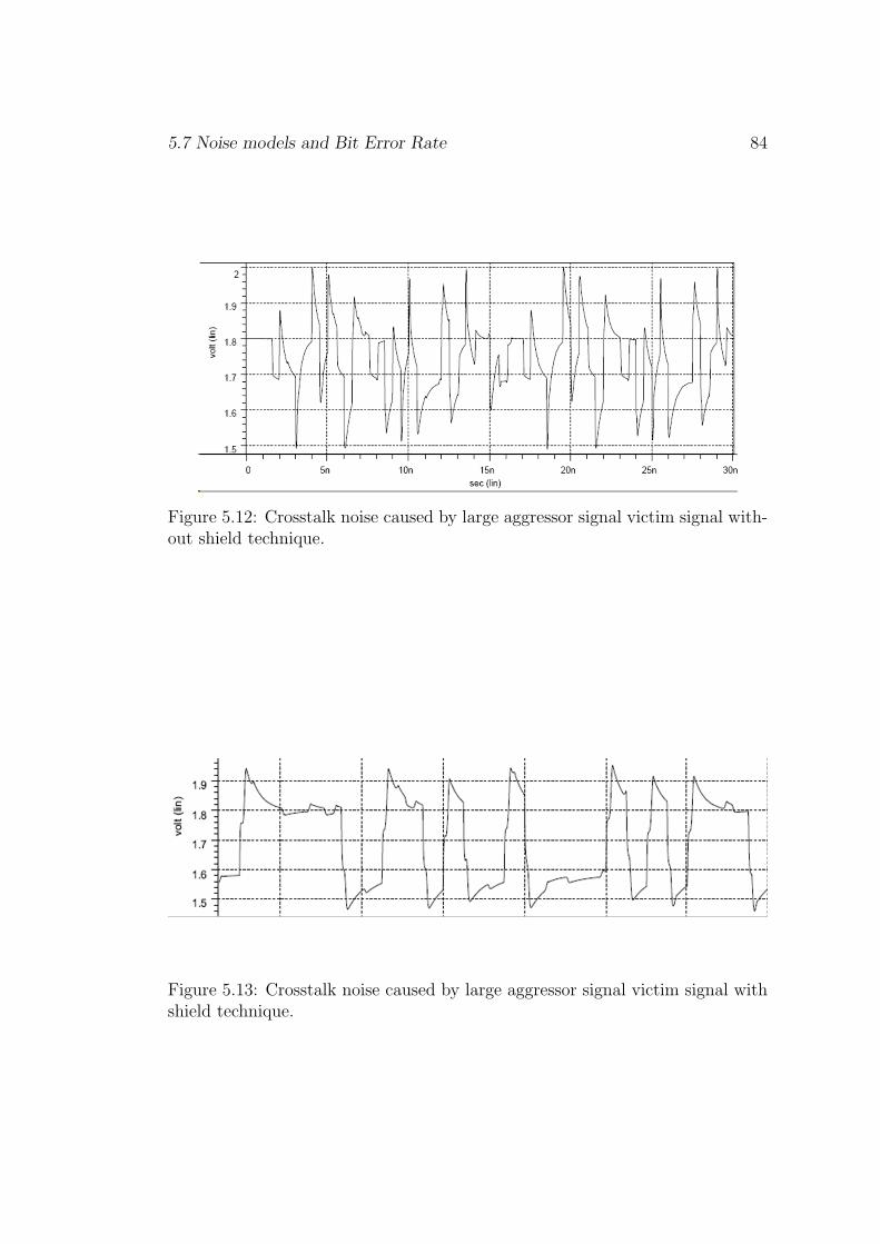
5.7 Noise models and Bit Error Rate 84
Figure 5.12: Crosstalk noise caused by large aggressor signal victim signal with-out shield technique.
Figure 5.13: Crosstalk noise caused by large aggressor signal victim signal withshield technique.

5.8 Simulation Results 85
Perr−pwm = Perr−Djitter + Perr−DIjitter (5.4)
Perr−pam = Perr−process + Perr−voltage + Perror−crosstalk (5.5)
Where Perr−pwm, Perr−pam, Perr−Djitter, Perr−DIjitter, Perr−process, Perr−voltage and
Perror−crosstalk are probabilities of error caused by PWM, PAM, DD(data de-
pendent) jitter, DI (data independent ) jitter, and process/voltage variation
including crosstalk, respectively. It can be assumed that all probabilities are
independent so there is no correlation between them. In this paper, all error
events are assumed having Gaussian distribution except Perror−crosstalk. There-
fore, all probabilities can be found by Monte Carlo simulation parameter and
PRBS-11 test bit patterns that cause crosstalk noise.
5.8 Simulation Results
5.8.1 Simulation setup
The technology parameters for the CNFETs are : Physical channel length =
32.0nm, The length of doped CNT drain-side/source-side extension region =
32.0nm , Fermi level of the doped S/D tube. = 0.6 eV, The thickness of high-k
top gate dielectric material = 4.0nm, chirality of tube = (19,0), Pitch = 10nm,
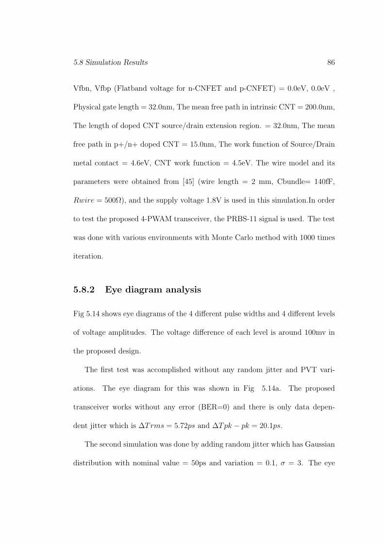
5.8 Simulation Results 86
Vfbn, Vfbp (Flatband voltage for n-CNFET and p-CNFET) = 0.0eV, 0.0eV ,
Physical gate length = 32.0nm, The mean free path in intrinsic CNT = 200.0nm,
The length of doped CNT source/drain extension region. = 32.0nm, The mean
free path in p+/n+ doped CNT = 15.0nm, The work function of Source/Drain
metal contact = 4.6eV, CNT work function = 4.5eV. The wire model and its
parameters were obtained from [45] (wire length = 2 mm, Cbundle= 140fF,
Rwire = 500Ω), and the supply voltage 1.8V is used in this simulation.In order
to test the proposed 4-PWAM transceiver, the PRBS-11 signal is used. The test
was done with various environments with Monte Carlo method with 1000 times
iteration.
5.8.2 Eye diagram analysis
Fig 5.14 shows eye diagrams of the 4 different pulse widths and 4 different levels
of voltage amplitudes. The voltage difference of each level is around 100mv in
the proposed design.
The first test was accomplished without any random jitter and PVT vari-
ations. The eye diagram for this was shown in Fig 5.14a. The proposed
transceiver works without any error (BER=0) and there is only data depen-
dent jitter which is ∆Trms = 5.72ps and ∆Tpk − pk = 20.1ps.
The second simulation was done by adding random jitter which has Gaussian
distribution with nominal value = 50ps and variation = 0.1, σ = 3. The eye
5.8 Simulation Results 87
diagram of this environment is shown in Fig 5.14b . As shown in the Fig
5.14b, the eye is almost 90% opened. As a result, the bit errors are too small
to measure. The third simulation is done by putting process variation with
Gaussian distribution which of 0.1 channel length and width variation and 3. Its
eye diagram is shown in Fig 5.13c. The eye is almost closed between 1.29 ∼ 1.49.
As the eye is getting closed, the bit error happens because of misreading in
comparator voltage level. In this case the bit error rate is expected to be less
than 10-10. The fourth simulation is combining the random jitter and process
variation used in second and third simulation. As shown in Fig 5.13d, the
only difference between the third and the fourth simulation result is the random
jitter increase. Because the random jitter in this case is not affecting the bit
error rate, the fourth simulation case has same bit error rate with the third one.
In order to see the effect of the supply voltage variation, another simulation was
done. The simulation of supply voltage variation was performed with Gaussian
distribution which has 0.01 ∼ 0.1 variations and σ = 3 for voltage. By changing
the voltage variation, it is observed that the eye opening is changing drastically.
Fig 5.12e shows eye-diagram for 0.01 variation and Fig 5.12f shows eye-diagram
for 0.5 variation. At 0.01 variation the eye is almost 60 ∼ 70% open and as the
variation goes over 0.5, the eye is completely closed.
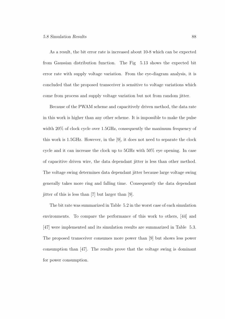
5.8 Simulation Results 88
As a result, the bit error rate is increased about 10-8 which can be expected
from Gaussian distribution function. The Fig 5.13 shows the expected bit
error rate with supply voltage variation. From the eye-diagram analysis, it is
concluded that the proposed transceiver is sensitive to voltage variations which
come from process and supply voltage variation but not from random jitter.
Because of the PWAM scheme and capacitively driven method, the data rate
in this work is higher than any other scheme. It is impossible to make the pulse
width 20% of clock cycle over 1.5GHz, consequently the maximum frequency of
this work is 1.5GHz. However, in the [9], it does not need to separate the clock
cycle and it can increase the clock up to 5GHz with 50% eye opening. In case
of capacitive driven wire, the data dependant jitter is less than other method.
The voltage swing determines data dependant jitter because large voltage swing
generally takes more ring and falling time. Consequently the data dependant
jitter of this is less than [7] but larger than [9].
The bit rate was summarized in Table 5.2 in the worst case of each simulation
environments. To compare the performance of this work to others, [44] and
[47] were implemented and its simulation results are summarized in Table 5.3.
The proposed transceiver consumes more power than [9] but shows less power
consumption than [47]. The results prove that the voltage swing is dominant
for power consumption.
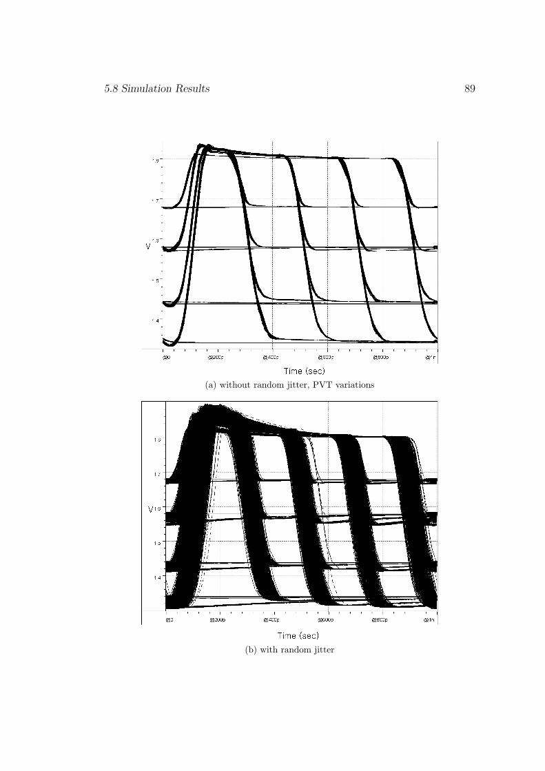
5.8 Simulation Results 89
(a) without random jitter, PVT variations
(b) with random jitter
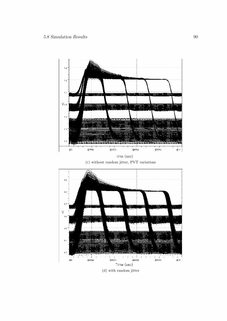
5.8 Simulation Results 90
(c) without random jitter, PVT variations
(d) with random jitter
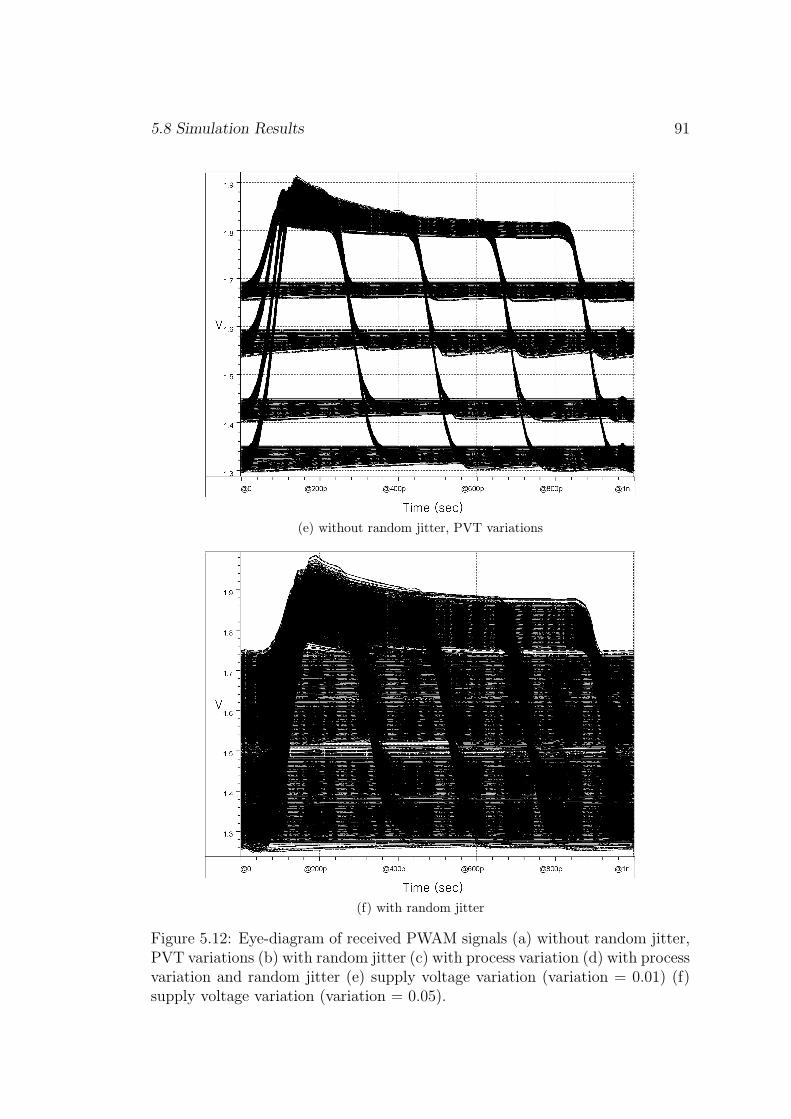
5.8 Simulation Results 91
(e) without random jitter, PVT variations
(f) with random jitter
Figure 5.12: Eye-diagram of received PWAM signals (a) without random jitter,PVT variations (b) with random jitter (c) with process variation (d) with processvariation and random jitter (e) supply voltage variation (variation = 0.01) (f)supply voltage variation (variation = 0.05).
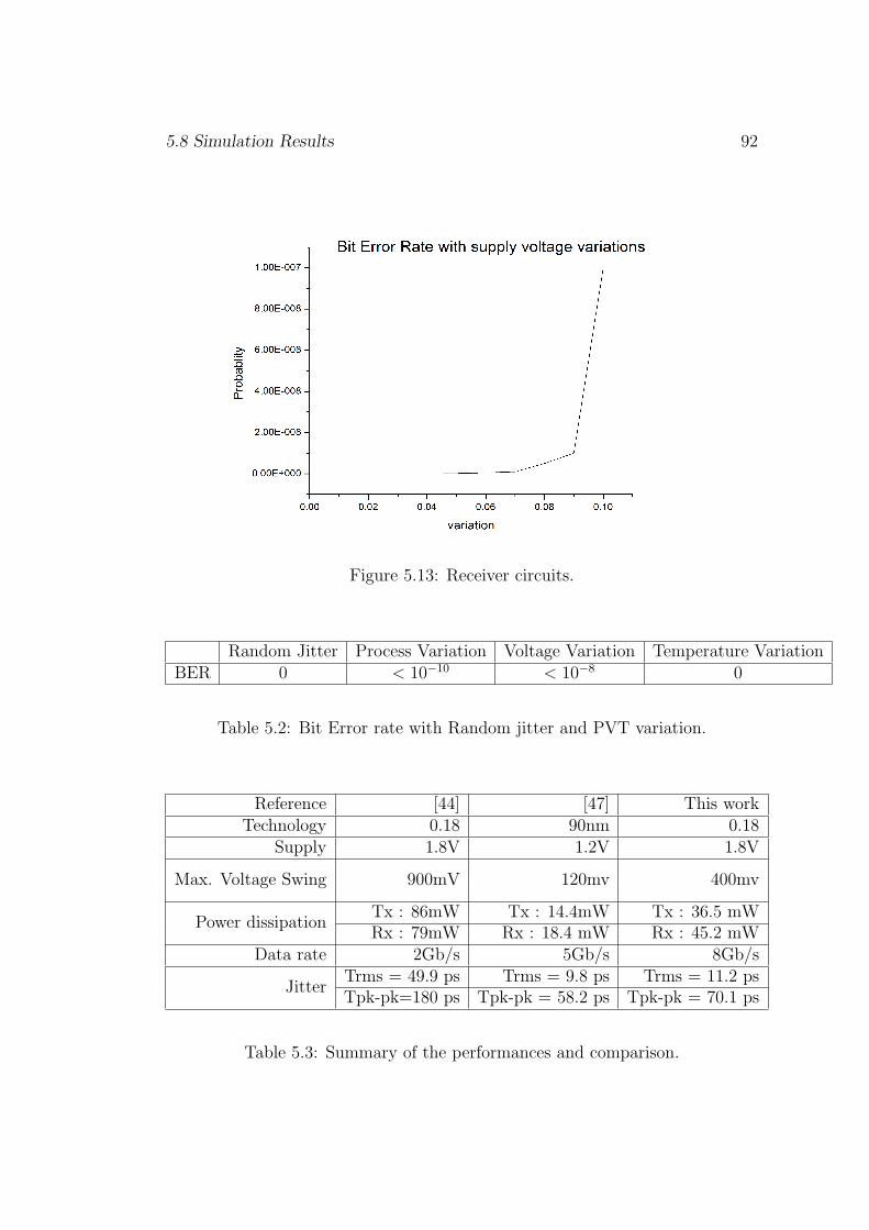
5.8 Simulation Results 92
Figure 5.13: Receiver circuits.
Random Jitter Process Variation Voltage Variation Temperature VariationBER 0 < 10−10 < 10−8 0
Table 5.2: Bit Error rate with Random jitter and PVT variation.
Reference [44] [47] This workTechnology 0.18 90nm 0.18
Supply 1.8V 1.2V 1.8V
Max. Voltage Swing 900mV 120mv 400mv
Power dissipationTx : 86mW Tx : 14.4mW Tx : 36.5 mWRx : 79mW Rx : 18.4 mW Rx : 45.2 mW
Data rate 2Gb/s 5Gb/s 8Gb/s
JitterTrms = 49.9 ps Trms = 9.8 ps Trms = 11.2 psTpk-pk=180 ps Tpk-pk = 58.2 ps Tpk-pk = 70.1 ps
Table 5.3: Summary of the performances and comparison.
5.9 Summary 93
5.9 Summary
In this chapter, capacitive 4-PWAM transmitter architecture is proposed and
its performances are analyzed with random jitter and PVT variation comparing
with other works. To implement 4-PWAM transmitter new phase controller and
adaptive capacitance network is designed. At the receiver side, new architecture
for PWM and PAM demodulation is proposed. The 4-PWAM transceiver in this
work has low data dependant jitter which does not affect the bit error rate. But
it is very sensitive to supply voltage variation. It is because voltage difference
between amplitude modulation is relatively low (100mv) which causes low noise
margin. But if the supply voltage variation is lower than 5%, the bit error rate
will be less than 10−10.
The proposed capacitive 4-PWAM transmitter with low swing voltage can
save a lot of power consumption comparing with the full swing one and other
PAM scheme. Furthermore it can increase data rate with PWAM modulation
and pre-emphasis . In this chapter, the proposed transceiver demonstrates that
almost 1.74 ∼ 2.4 times power is saved compared to [44] and 4 times higher data
rate than [47] is accomplished.
Chapter 6
Conclusion
6.1 Conclusion
The Carbon Nanotube Field Effect Transistor (CNTFET) is one of the most
promising devices among emerging technologies to extend and/or complement
the traditional Si MOSFET. As the characteristics of a CNTFET is different
from conventional bulk CMOS, new design method must be established. As
demand of new design method, this thesis analyze the characteristics of CNFET,
CNT interconnect technologies and propose new methodologies to design circuits
such as digital, memory and I/O circuit.
The quantitative results of chapter 2 have confirmed that the CNTFET tech-
nology is a viable solution to replace the conventional bulk MOSFET technology

6.1 Conclusion 95
and, in particular, this work makes it possible to quantitatively estimate the de-
lay, leakage current, and power of CNTFET-based gates.
This has been accomplished by proposing a new optimization methodology
for CNTFETs in chapter 3. The parameters such as threshold voltage,gate
capacitance, drain current, optimum fan-out factor can be determined by pitch,
chirality and the number of carbon nano tubes. Using these parameter, the
logical effort has been calculated and the minimum delay of a multistage circuit
topology has been analyzed. To prove the effectiveness of the proposed gate-
level design method, simulation has been performed using HSPICE with the
CNTFET library of [22][17], Results have demonstrated that the proposed design
methodology is both effective and practical . To design a CNFET circuit, many
parameters must be considered, among them the diameter at certain chirality,
pitch and the optimum number of tubes have been shown to be of primary
importance.
In chapter 4, new SRAM circuit was proposed. The new SRAM cell cuts off
the feedback connection between the two back-to-back inverters in the SRAM
cell when data is written and separates the write and read port with 8 transistors.
The proposed technique saves dynamic power by reducing discharging frequency
during write operation. Compared to 6T SRAM structure, the proposed 8T
SRAM for CNFET saves power up to 48% and obtains 56% wider SNM during
read operation at the minimal cost of 2% leakage power and 3% delay increase.
6.1 Conclusion 96
As the cells are more frequently accessed, the dynamic power saving is linearly
increased. This work also compares CMOS, FinFET and CNT 6T and 8T
SRAM cells using HSPICE simulations. The result demonstrates from 3 to 7
times less dynamic power consumption, from 11 to17 times less leakage power
consumption, from 5 to 6 times faster read and write operations, and 1.6 wider
SNM than the conventional CMOS designs
In chapter 5 , capacitive 4-PWAM transceiver architecture for CNFET and
CNT interconnect technologies is proposed and its performances are analyzed
with random jitter and PVT variation comparing with other works as an I/O
circuits. The characteristics such as wire capacitance, resistance and inductance
of CNT bundle and gate capacitance, analog parameters of CNFET was an-
alyzed to design transceiver. To implement 4-PWAM transmitter new phase
controller and adaptive capacitance network is designed. At the receiver side,
new architecture for PWM and PAM demodulation is proposed. The 4-PWAM
transceiver in this work has low data dependant jitter which does not affect the
bit error rate. But it is very sensitive to supply voltage variation. It is because
voltage difference between amplitude modulation is relatively low (100mv) which
causes low noise margin. But if the supply voltage variation is lower than 5%,
the bit error rate will be less than 10−10. The proposed CNFET capacitive 4-
PWAM transceiver with low swing voltage can save a lot of power consumption
comparing with the full swing one and other PAM scheme. Furthermore it can
6.1 Conclusion 97
increase data rate with PWAM modulation and pre-emphasis [5]. In this work,
the proposed transceiver demonstrates that almost 1.74 ∼ 2.4 times power is
saved compared to [7] and 4 times higher data rate than [9] is accomplished.
This research presents a development of systematic design method to op-
timize circuit speed and power consumption. In this thesis,three optimization
methods are proposed and some traditional CMOS circuits are modified for CN-
FET and CNT interconnect technologies. The optimization methods explored
in this thesis include digital circuit design, memory circuit design and high speed
on chip I/O circuits. In order to test the effectiveness of the design method, CN-
FET and CNT interconnect models have been developed and extensive HSPICE
simulations have been performed in realistic environments considering screening
effects, various noises and PVT variation. The simulation results show that pro-
posed methodologies and modified circuits performed high speed and consumed
low power compared to non-optimized and traditional circuits.
Bibliography
[1] Data from http://www.itrs.net/Links/2005ITRS/Home2005.htm
[2] J. Deng, N. Patil, K. Ryu, A. Badmaev, C. Zhou, S. Mitra, H.-S. P. Wong,
’Carbon Nanotube Transistor Circuits: Circuit-Level Performance Bench-
marking and Design Options for Living with Imperfections’ International
Solid State Circuits Conference (ISSCC), pp. 70-71, San Francisco, CA,
February, 2007.
[3] A. Javey, J. Guo, D. B. Farmer, Q. Wang, E. Yenilmez, R. G. Gordon,
M. Lundstrom, H. Dai, ’Self-Aligned Ballistic Molecular Transistors and
Electrically Parallel Nanotube Arrays’ Nano Letters, vol. 4, pp. 1319-1322,
2004.
[4] A. Javey, R. Tu, D.B. Farmer, J. Guo, R.G. Gordon, H. Dai, ’High Perfor-
mance n-Type Carbon Nanotube Field-Effect Transistors with Chemically
Doped Contacts’ Nano Letters, vol. 5, pp. 345-348, 2005.
[5] D. Mann, A. Javey, J. Kong, Q. Wang, and H. Dai, ’Ballistic Transport in
Metallic Nanotubes with Reliable Pd Ohmic Contacts’ Nano Letters, vol.
3, pp. 1541-1544, 2003.
[6] J. Kedzierski, P. Xuan, E.H. Anderson, J. Bokor, T-J. King, C. Hu, ’Com-
plementary silicide source/drain thin-body MOSFETs for the 20 nm gate
length regime’ IEDM, pp.57-60, 2000.
BIBLIOGRAPHY 99
[7] [J. Appenzeller, J. Knoch, R. Martel, V. Derycke, S.J. Wind, Ph. Avouris,
’Carbon Nanotube Electronics’ IEEE Trans. Nanotech., vol. 1, no. 4, pp.
184-189, 2002.
[8] M. Horowitz, E. Alon, D. Patil, ’Scaling, Power, and the Future of CMOS’
IEDM Tech. Digest, pp. 11-14, 2005.
[9] R. Saito, G. Dresselhaus, and M. S. Dresselhaus, ’Physical Properties of
Carbon Nanotubes’ Imperial College Press, London, 1998.
[10] Z. Yao, C. L. Kane, and C. Dekker, ’High-field Electrical Transport In
Single-Wall Carbon Nanotubes’ Phys. Rev. Lett., vol. 84, pp. 2941-2944,
2000.
[11] M. S. Fuhrer, B. M. Kim, T. Dkop, and T. Brintlinger, ’High-Mobility
Nanotube Transistor Memory’ Nano Letters, vol. 2, pp. 755-759, 2002.
[12] Paul L. McEuen, Michael S. Fuhrer, and Hongkun Park, ’Single-Walled
Carbon Nanotube Electronics’ IEEE Trans. Nanotech., vol. 1, pp. 78-85,
2002.
[13] G. Pennington and N. Goldsman, ’Semiclassical Transport and Phonon
Scattering of Electrons in Semiconducting Carbon Nanotubes’ Phys. Rev.
B., vol.68, pp. 045426, 2003.
[14] B. Q. Wei, R. Vajtai, and P. M. Ajayan, ’Reliability and Current Carrying
Capability of Carbon Nanotubes’ Appl. Phys. Lett., vol. 79, pp. 1172-1174,
2001.
[15] Y. Cui, Z. Zhong, D. Wang, W. U. Wang, and C. M. Lieber, ’High Perfor-
mance Silicon Nanowire Field Effect Transistors’ Nano Letters, vol. 3, pp.
149-152, 2003.
BIBLIOGRAPHY 100
[16] A. Javey, J. Guo, D. B. Farmer, Q. Wang, D. Wang, R. G. Gordon, M.
Lundstrom, and H. Dai, ’Carbon Nanotube Field-Effect Transistors with
Integrated Ohmic Contacts and High-k Gate Dielectrics’ Nano Letters, vol.
4, pp. 447-450, 2004.
[17] Z. Chen, J. Appenzeller, P. M. Solomon, Y.-M. Lin, P. Avouris, ’Gate
Work Function Engineering for Nanotube-Based Circuits’ International
Solid State Circuits Conference (ISSCC), p. 68 69, 2007.
[18] R. Martel, V. Derycke, C. Lavoir, J. Appenzeller, K. K. Chan, J. Ter-
soff, and Ph. Avouris, ’Ambipolar Electrical Transport in Semiconducting
Single-wall Carbon Nanotubes’ Phys, Rev. Lett., vol 87, pp. 256805, 2001.
[19] A. Javey, J. Guo, D. B. Farmer, Q. Wang, D. Wang, R. G. Gordon, M.
Lundstrom, and H. Dai ”Carbon nanotube field-effect transistors with in-
tegrated ohmic contacts and high-k gate dielectrics” Nano Letters, vol. 4,
no. 3, pp. 447-450, 2004
[20] J. Guo, M. Lundstrom, and S. Datta ”Performance projections for ballistic
carbon nanotube field-effect transistors,” Applied Physics Letters, vol. 80,
pp. 3192-3194, 2002.
[21] A. Naeemi, R. Sarvari, and J. D. Meindl ”Performance comparison between
carbon nanotube and copper interconnects for gigascale integration (GSI),”
Electron Device Letters, IEEE, vol. 26, pp. 84-86,2005.
[22] J. Deng, and H.-S. P. Wong ”A Circuit-Compatible SPICE model for En-
hancement Mode Carbon Nanotube Field Effect Transistors,” Proc. Intl.
Conf. Simulation of Semiconductor Processes and Devices, pp. 166 - 169,
Sept., 2006.
[23] I. Amlani, et al ”First Demonstration of AC Gain From a Single-walled
BIBLIOGRAPHY 101
Carbon Nanotube Common-Source Amplifier,” Proc. Intl. Electron Devices
Meeting, Paper 20.7, Dec., 2006.
[24] http://www eas.asu.edul-ptm/latest.html
[25] A. Bhavnaganwala, X. Tang, and J. D. Meindl ”The Impact of Intrin-
sic Device Fluctuations on CMOS SRAM Cell Stability,” IEEE Journal of
Solid-State Circuits, , Vol. 36, No. 4, pp. 658-665. April 2001.
[26] J. Deng and H.-S. P.Wong ”A compact SPICE model for carbon nanotube
field effect transistors including non-idealities and its applicationPart II:
Full device model and circuit performance benchmarking,” IEEE Trans.
JElectron Devices, vol. 54, no. 12, pp. 3195-3205, Dec. 2007.
[27] Jing Guo, et al. ”Predicted Performance Advantages of Carbon Nanotube
Transistors with Doped Nanotubes as Source/Drain”.Condensed Matter,
0309039, 2003.
[28] Kyung Ki Kim and Yong-Bin Kim, ’Design Methodology for Power Supply
Noise and Leakage Current Control in Nanoscale CMOS VLSI Systems
Design’ IEEE Transactions on VLSI Systems(accepted).
[29] Yong-Bin Kim and Kyung Ki Kim ”Optimal Body Biasing for Minimum
Leakage Power in Standby Mode” IEEE International Symposium on Cir-
cuits and Systems, New Orleans, LA, May 27-30, 2007, pp.1161-1164.
[30] J.Deng, H.-S P. Wong ”Modeling and Analysis of Planar Gate Electrostatic
Capacitance for 1-D FET with Multiple Cylindrical Conducting Channels”.
IEEE Trans. Electron Devices, Vol. 54 p. 2377-2385, 2007
[31] Nils Hedenstierna, Kjell O. Jeppson ”CMOS Circuit Speed and Buffer
Optimization ” IEEE Trans. Computer-aided Design, Vol. CAD-6, NO. 2,
p. 270-281, 1987
BIBLIOGRAPHY 102
[32] Ivan E. Sutherland, Robert F. Sproull, and David F. Harris ”Logical Effort:
Designing Fast CMOS Circuits” Margan Kaufmann
[33] P. Avouris, J. Appenzeller, V. Derycke, R. Martel, and S. Wind ”Carbon
nanotube electronics” IEEE IEDM ,Dec, p. 281-284, . 2002.
[34] Arijit Raychowdhury, Saibal Mukhopadhyay , Kaushik Roy ”Circuit-
Compatible Modeling ob Carbon Nanotube FETs in the Ballistic Limit
of Performance” IEEE NANO vol.2, p. 343-346, 2003
[35] J. Deng, N. Patil, K. Ryu, A. Badmaev, C. Zhou, S. Mitra, H.-S. P. Wong
”Carbon Nanotube Transistor Circuits: Circuit-Level Performance Bench-
marking and Design Options for Living with Imperfections,” IEEE ISSCC
, pp 70-71, 2007
[36] Tawfik, S.A. Kursun, V. ”Low-Power and Compact Sequential Circuits
With Independent-Gate FinFETs”, Electron Devices, IEEE Transactions
vol. 55, No. 1, pp. 60-70, Jan 2008
[37] A. Bhavnaganwala, X. Tang, and J. D. Meindl ”The Impact of Intrinsic
Device Fluctuations on CMOS SRAMCell Stability” IEEE Journal of Solid-
State Circuits, , Vol. 36, No. 4, pp. 658-665. April 2001
[38] R. Ho, K. W. Mai, and M. A. Horowitz The future of wires Proc. IEEE,
vol. 89, no. 4, pp. 490-504, Apr. 2001.
[39] L. Benini and G. De Micheli Networks on chips: A new SoC paradigm IEEE
Computer, vol. 35, no. 1, pp. 70.78, Jan. 2002.
[40] W. J. Dally and B. Towles Route packets, not wires: On-chip interconnec-
tion networks in Proc. 38th Des. Autom. Conf., Jun. 2001, pp. 684-689
BIBLIOGRAPHY 103
[41] Ramin Farjad-Rad, Chih-Kong Ken Yang, Mark A. Horowitz, and Thomas
H Lee. ”A 0.4-um CMOS 10-Gb/s 4-PAM Pre-emphasis Serial Link Trans-
mitter IEEE JOURNAL OF SOLID-STATE CIRCUITS,34(5):580-585,
May 1999.
[42] Ramin Farjad-Rad, Chih-Kong Ken Yang, Mark A. Horowitz, and Thomas
H Lee. ”A 0.3.m CMOS 8-Gb/s 4-PAM Serial Link Transceiver IEEE
JOURNAL OF SOLID-STATE CIRCUITS, 35(5):757-764, May 2000.
[43] Wei-Hung Chen, Guang-Kaai Dehng, Jong-Woei Chen, and Shen-Iuan Liu
”A CMOS 400-Mb/s serial link for AS-memory systems using a PWM
scheme” IEEE JOURNAL OF SOLID-STATE CIRCUITS, 36(10):1498-
1505, October 2001.
[44] Rui tang, Yong-Bin Kim, ”Energy Efficient CMOS PWAM Transmitter
Design,” IEEE Midwest Symposium on Circuit and Systems, August 5-8,
2007, Montreal, Canada, pp.1161-1164.
[45] A. Raychowdhury and K. Roy Modeling of metallic carbon nanotube in-
terconnects for circuit simulations and a comparison with Cu interconnects
for scaled technologies IEEE Transactions on Computer-Aided Design of
Integrated Circuits and Systems, vol. 25, no.1, pp. 58-65, 2006
[46] R. Ho, T. Ono, F. Liu, R. Hopkins, A. Chow, J. Schauer, and R. Drost
”High-speed and low-energy capacitively-driven on-chip wires” in IEEE
ISSCC Dig. Tech. Papers, 2007, pp. 412-441
[47] Daniel Schinkel,Eisse Mensink, Eric A. M. Klumperink,Ed van Tuijl, Bram
Nauta, ”Low-Power, High-Speed Transceivers for Network-on-Chip Com-
munication” IEEE Transactions on Very Large Scale Integration Systems,
vol. 17, no. 1, January2009
BIBLIOGRAPHY 104
[48] K. Lee, S.-J. Lee, S.-E. Kim, H.-M. Choi, D. Kim, S. Kim, M.-W. Lee, and
H.-J. Yoo A 51 mW 1.6 GHz on-chip network for low-power heterogeneous
SoC platform in IEEE ISSCC Dig. Tech. Papers, Feb.2004, pp. 152-153
[49] H. Zhang, V. George, and J. M. Rabaey Low-swing on-chip signaling tech-
niques: Effectiveness and robustness IEEE Trans. Very Large Scale Integr.
(VLSI) Syst., vol. 8, no. 3, pp. 264.272, Jun. 2000.
[50] D. Schinkel, E. Mensink, E. A. M. Klumperink, E. van Tuijl, and B. Nauta
A 3-Gb/s/ch transceiver for 10-mm uninterrupted RC-limited global on-
chip interconnects IEEE J. Solid-State Circuits, vol. 41, no.1, pp. 297-306,
Jan. 2006.
[51] L. Zhang, J. Wilson, R. Bashirullah, L. Lei, X. Jian, and P. Franzon Driver
pre-emphasis techniques for on-chip global buses in Proc. Int.Symp. Low
Power Electron. Des. (ISLPED), Aug. 2005, pp. 186-191.
[52] F. Worm, P. Ienne, P. Thiran, and G. De Micheli, A robust self-calibrating
transmission scheme for on-chip networks, IEEE Trans. Very Large Scale
Integr. (VLSI) Syst., vol. 13, no. 1, pp. 126-139, Jan. 2005.
[53] ”HSPICE User Guide: Simulation and Analysis” Version C-2009, pp.763-
782.
[54] A. Vittal, L. H. Chen, S. M. Marek, K.-P. Wang, and X. Yang, ”Crosstalk in
VLSI Interconnections,” IEEE Transactions on Computer-Aided Desgin of
Integrated Circuits and Systems, Vol. 18, No. 12, pp. 1817- 1824, December
1999.


![Low Leakage CNTFET SRAM Cells - core.ac.uk · performed with Stanford CNTFET model at 32nm feature size with supply voltage V DD of 0.9V [13]. The](https://img.pdfslide.us/doc/110x75/5b0966b57f8b9a992a8d9376/low-leakage-cntfet-sram-cells-coreacuk-with-stanford-cntfet-model-at-32nm-feature.jpg)