Embed Size (px)
Citation preview
www.maxim-ic.com
DS26503DK T1/E1/J1 BITS Element
Design Kit
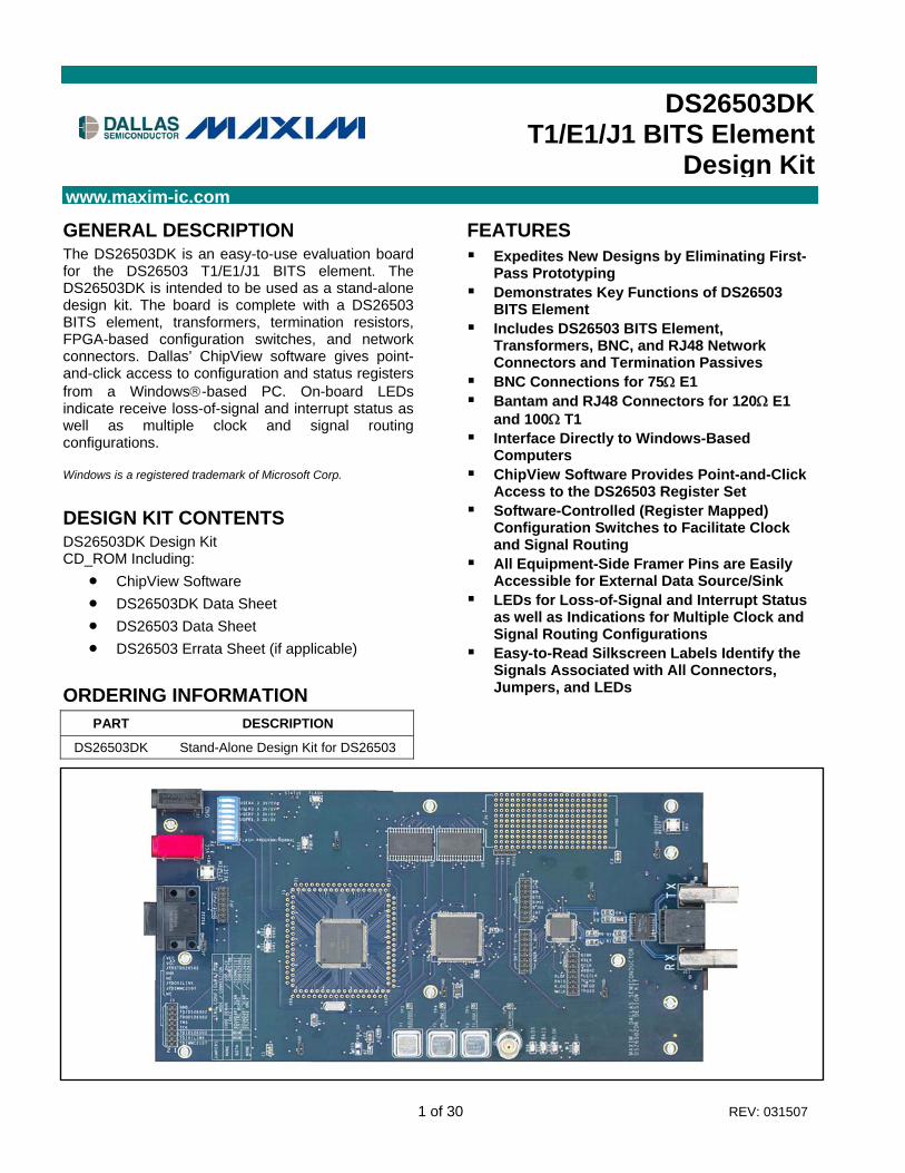
GENERAL DESCRIPTION The DS26503DK is an easy-to-use evaluation board for the DS26503 T1/E1/J1 BITS element. The DS26503DK is intended to be used as a stand-alone design kit. The board is complete with a DS26503 BITS element, transformers, termination resistors, FPGA-based configuration switches, and network connectors. Dallas’ ChipView software gives point-and-click access to configuration and status registers from a Windows®-based PC. On-board LEDs indicate receive loss-of-signal and interrupt status as well as multiple clock and signal routing configurations. Windows is a registered trademark of Microsoft Corp. DESIGN KIT CONTENTS DS26503DK Design Kit CD_ROM Including:
• ChipView Software • DS26503DK Data Sheet • DS26503 Data Sheet • DS26503 Errata Sheet (if applicable)
ORDERING INFORMATION
PART DESCRIPTION
DS26503DK Stand-Alone Design Kit for DS26503
1 of 30 REV: 031507
FEATURES Expedites New Designs by Eliminating First-
Pass Prototyping Demonstrates Key Functions of DS26503
BITS Element Includes DS26503 BITS Element,
Transformers, BNC, and RJ48 Network Connectors and Termination Passives
BNC Connections for 75Ω E1 Bantam and RJ48 Connectors for 120Ω E1
and 100Ω T1 Interface Directly to Windows-Based
Computers ChipView Software Provides Point-and-Click
Access to the DS26503 Register Set Software-Controlled (Register Mapped)
Configuration Switches to Facilitate Clock and Signal Routing
All Equipment-Side Framer Pins are Easily Accessible for External Data Source/Sink
LEDs for Loss-of-Signal and Interrupt Status as well as Indications for Multiple Clock and Signal Routing Configurations
Easy-to-Read Silkscreen Labels Identify the Signals Associated with All Connectors, Jumpers, and LEDs
DS26503DK
2 of 30
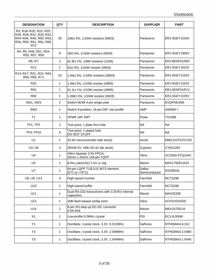
COMPONENT LIST
DESIGNATION QTY DESCRIPTION SUPPLIER PART
C1, C4, C23, C51, C53 5 10μF 20%, 10V ceramic capacitors (1206) Panasonic ECJ-3YB1A106M
C2–C3, C6–C9, C11, C12, C14, C15, C17, C18, C20, C21, C25–C30, C32,
C33, C35, C36, C38, C45–C50, C52, C54, C55, C57–C60, C62, C63, C68
41 1μF 10%, 16V ceramic capacitors (1206) Panasonic ECJ-3YB1C105K
C5, C10, C22, C24, C31, C34, C37, C39–C41, C43,
C65–C67, C69, C70 16 0.1μF 20%, 16V X7R ceramic capacitors (0603) AVX 0603YC104MAT
C13, C19, C42, C44, C64 5 10μF 20%, 16V tantalum capacitors (B case) Panasonic ECS-T1CX106R
C16, C56, C61 3 68μF 20%, 16V tantalum capacitors (D case) Panasonic ECS-T1CD686R
D1 1 1A 50V general-purpose silicon diode General Semiconductor 1N4001
DS1, DS2, DS6–DS9 6 Red LEDs, SMD Panasonic LN1251C
DS3 1 Green LED, SMD Panasonic LN1351C
DS4 1 Amber LED, SMD Panasonic LN1451C
DS5 1 Green LED, SMD (Not populated) Panasonic LN1351C
DS10 1 Red/green LED, 5mm right-angle PCMT Digi-Key 350-1055-ND
J1 1 Socket, banana plug, horizontal, black Mouser Electronics 164-6218
J2 1 Socket, banana plug, horizontal, red Mouser Electronics 164-6219
J3, J6–J8 4 Terminal strip, 16-pin, dual row, vertical Samtec TSW-108-07-T-D
J4 1 DB9 right-angle, long case connector AMP 747459-1
J5 1 75Ω vertical 5-pin BNC connector Cambridge CP-BNCPC-004
J9 1 RJ48 8-pin, single-port connector MOLEX 15-43-8588
J10, J11 2 BNC connectors, 75Ω right-angle 5-pin Kruvand UCBJR220
J12, J13 2 Bantam jack, right-angle connectors Switchcraft RTT34B02
JP1, JP3–JP8 7 100-mil, 2-position jumper labstock
JP2 1 14-pin header, remove 'missing pin' labstock
L1 1 Inductor, 22.0μH 2-pin SMT 20% Coiltronics UP1B-220
NP1, NP2 2 10pF 5%, 50V tall case ceramic capacitors (1206)Do not populate Phycomp 1206CG100J9B200
R1, R8–R11 5 0Ω 5%, 1/8W resistors (1206) Panasonic ERJ-8GEYJ0R00V R2, R13, R23, R27, R43,
R47, R67–R70 10 330Ω 5%, 1/16W resistors (0603) Panasonic ERJ-3GEYJ331V
DS26503DK
3 of 30
DESIGNATION QTY DESCRIPTION SUPPLIER PART
R3, R18–R20, R22, R25, R26, R28–R31, R33–R42, R44–R46, R49, R50, R53, R56, R59, R61, R62, R65,
R72
33 10kΩ 5%, 1/16W resistors (0603) Panasonic ERJ-3GEYJ103V
R4, R5, R48, R51, R54, R55, R57, R58 8 30Ω 5%, 1/16W resistors (0603) Panasonic ERJ-3GEYJ300V
R6, R7 2 61.9Ω 1%, 1/8W resistors (1206) Panasonic ERJ-8ENF61R9V
R12 1 51Ω 5%, 1/16W resistor (0603) Panasonic ERJ-3GEYJ510V
R14–R17, R21, R24, R63, R64, R66, R71 10 1.0kΩ 5%, 1/16W resistors (0603) Panasonic ERJ-3GEYJ102V
R32 1 1.0kΩ 5%, 1/10W resistor (0805) Panasonic ERJ-6GEYJ102V
R52 1 51.1Ω 1%, 1/10W resistor (0805) Panasonic ERJ-6ENF51R1V
R60 1 1.0MΩ 5%, 1/16W resistor (0603) Panasonic ERJ-3GEYJ105V
SW1, SW3 2 Switch MOM 4-pin single pole Panasonic EVQPAE04M
SW2 1 Switch 8-position, 16-pin DIP, low profile AMP 435668-7
T1 1 XFMR 16P SMT Pulse TX1099
TP1, TP2 2 Test point, 1 plate thru-hole NA NA
TP3–TP10 8 Test point, 1 plated hole DO NOT STUFF NA NA
U1 1 32-bit microcontroller (lab stock) Avnet MMC2107CFCV33
U3, U6 2 SRAM 5V, 1Mb SO (in lab stock) Cypress CY62128V
U4 1 Xilinx Spartan 2.5V FPGA, 20mm x 20mm 144-pin TQFP Xilinx XC2S50-5TQ144C
U5 1 8-Pin μMAX/SO 2.5V or Adj Maxim MAX1792EUA25
U7 1 64-pin LQFP T1/E1/J1 BITS element (0°C to +70°C)
Dallas Semiconductor DS26503L
U8, U9, U13 3 High-speed inverter Fairchild NC7SZ86
U10 1 High-speed buffer Fairchild NC7SZ86
U11 1 Dual RS-232 transceivers with 3.3V/5V internal capacitors Maxim MAX3233E
U12 1 1Mb flash-based config mem Xilinx XCF01SV020C
U14 1 8-pin SO step-up DC-DC converter 0.5A limit Maxim MAX1675EUA
X1 1 Low-profile 8.0MHz crystal PEI EC1-8.000M
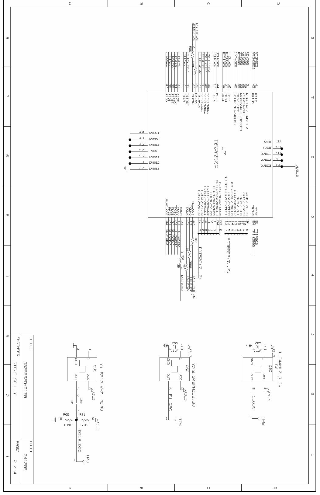
Y1 1 Oscillator, crystal clock, 3.3V, 6.312MHz SaRonix NTH069A3-6.312
Y2 1 Oscillator, crystal clock, 3.3V, 2.048MHz SaRonix NTH039A3-2.0480
Y3 1 Oscillator, crystal clock, 3.3V, 1.544MHz SaRonix NTH039A3-1.5440
DS26503DK
4 of 30
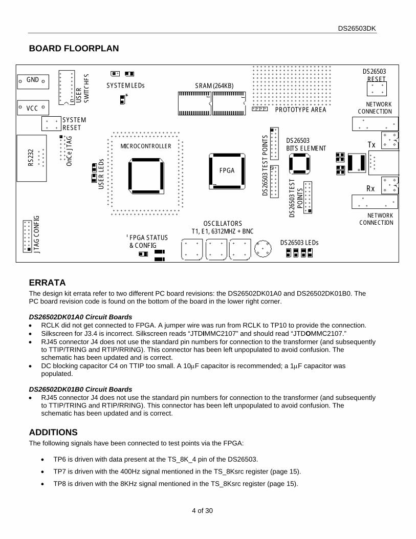
BOARD FLOORPLAN
GND
VCC
RS23
2
OnCe
JTAG
MICROCONTROLLER
SRAM (264KB)
FPGA
DS26503 BITS ELEMENT
DS26
503 T
EST
POIN
TS
DS26
503 T
EST
POIN
TS
ERRATA The design kit errata refer to two different PC board revisions: the DS26502DK01A0 and DS26502DK01B0. The PC board revision code is found on the bottom of the board in the lower right corner. DS26502DK01A0 Circuit Boards • RCLK did not get connected to FPGA. A jumper wire was run from RCLK to TP10 to provide the connection. • Silkscreen for J3.4 is incorrect. Silkscreen reads “JTDIMMC2107” and should read “JTDOMMC2107.” • RJ45 connector J4 does not use the standard pin numbers for connection to the transformer (and subsequently
to TTIP/TRING and RTIP/RRING). This connector has been left unpopulated to avoid confusion. The schematic has been updated and is correct.
• DC blocking capacitor C4 on TTIP too small. A 10μF capacitor is recommended; a 1μF capacitor was populated.
DS26502DK01B0 Circuit Boards • RJ45 connector J4 does not use the standard pin numbers for connection to the transformer (and subsequently
to TTIP/TRING and RTIP/RRING). This connector has been left unpopulated to avoid confusion. The schematic has been updated and is correct.
ADDITIONS The following signals have been connected to test points via the FPGA:
• TP6 is driven with data present at the TS_8K_4 pin of the DS26503.
• TP7 is driven with the 400Hz signal mentioned in the TS_8Ksrc register (page 15).
• TP8 is driven with the 8KHz signal mentioned in the TS_8Ksrc register (page 15).
JTAG
CON
FIG
FPGA STATUS & CONFIG
OSCILLATORS T1, E1, 6312MHZ + BNC
DS26503 LEDs
USER
LEDs
PROTOTYPE AREA
SYSTEM LEDs
NETWORKCONNECTION
NETWORK CONNECTION
Rx
Tx
DS26503RESET
SYSTEM RESET
USER
SW
ITCH
ES
DS26503DK
5 of 30
BASIC OPERATION This design kit relies upon several supporting files, which are available for downloading on our website at www.maxim-ic.com/telecom. See the DS26503DK QuickView data sheet for these files.
Hardware Configuration • Supply 3.3V to the banana-plug receptacles marked GND and VCC_3.3V. • DIP switches are unused and can be in either the ON or OFF position with exception for the Flash
programming switch, which should be OFF. • From the Programs menu, launch the host application named ChipView.exe. Run the ChipView application. If
the default installation options were used, click the Start button on the Windows toolbar and select Programs → ChipView → ChipView.
General • Upon power-up the RLOS and RLOF LEDs (red) will be lit, the INT LED (red) will not be lit, and Status LED
(DS10 red/green bicolor) will be green.
Quick Setup (Register View) • The PC will load ChipView offering a choice among DEMO MODE, REGISTER VIEW, and TERMINAL MODE.
Select Register View. • The program will then request a definition file. Select DS26503DC_FPGA.def. Through the ‘links’ section, this
will also load DS26503.def. • The Register View Screen will appear, showing the register names, acronyms, and values for the DS26503. • Predefined Register settings for several functions are available as initialization files.
• ini files are loaded by selecting the menu File→Reg ini File→Load ini File. • Load the ini file “CompositeClock.ini.” • Load the ini file “DS26502FPGA_2048Clks.ini,” which sets the DS26503 in Intel nonmultiplexed mode with
MCLK driven at 2.048MHz. • After loading the ini files the following may be observed:
• The RLOS and RLOF LEDs extinguishes upon external loopback. • The part begins operating in composite clock mode.
Miscellaneous • Clock frequencies and certain pin bias levels are provided by a register-mapped FPGA. • The definition file for this FPGA is named DS26503DC_FPGA.def. Table 2 shows the FPGA register
definitions. A drop-down menu on the top of the screen allows for switching between definition files. • All files referenced above are available for download as described in the section marked “BASIC
OPERATION.”
DS26503DK
6 of 30
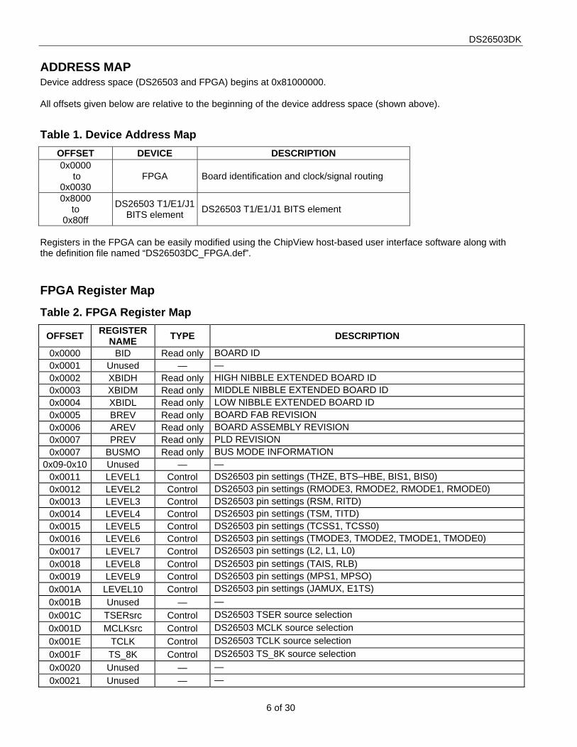
ADDRESS MAP Device address space (DS26503 and FPGA) begins at 0x81000000. All offsets given below are relative to the beginning of the device address space (shown above). Table 1. Device Address Map
OFFSET DEVICE DESCRIPTION 0x0000
to 0x0030
FPGA Board identification and clock/signal routing
0x8000 to
0x80ff
DS26503 T1/E1/J1 BITS element DS26503 T1/E1/J1 BITS element
Registers in the FPGA can be easily modified using the ChipView host-based user interface software along with the definition file named “DS26503DC_FPGA.def”.
FPGA Register Map
Table 2. FPGA Register Map
OFFSET REGISTER NAME TYPE DESCRIPTION
0x0000 BID Read only BOARD ID 0x0001 Unused — — 0x0002 XBIDH Read only HIGH NIBBLE EXTENDED BOARD ID 0x0003 XBIDM Read only MIDDLE NIBBLE EXTENDED BOARD ID 0x0004 XBIDL Read only LOW NIBBLE EXTENDED BOARD ID 0x0005 BREV Read only BOARD FAB REVISION 0x0006 AREV Read only BOARD ASSEMBLY REVISION 0x0007 PREV Read only PLD REVISION 0x0007 BUSMO Read only BUS MODE INFORMATION
0x09-0x10 Unused — — 0x0011 LEVEL1 Control DS26503 pin settings (THZE, BTS–HBE, BIS1, BIS0) 0x0012 LEVEL2 Control DS26503 pin settings (RMODE3, RMODE2, RMODE1, RMODE0) 0x0013 LEVEL3 Control DS26503 pin settings (RSM, RITD) 0x0014 LEVEL4 Control DS26503 pin settings (TSM, TITD) 0x0015 LEVEL5 Control DS26503 pin settings (TCSS1, TCSS0) 0x0016 LEVEL6 Control DS26503 pin settings (TMODE3, TMODE2, TMODE1, TMODE0) 0x0017 LEVEL7 Control DS26503 pin settings (L2, L1, L0) 0x0018 LEVEL8 Control DS26503 pin settings (TAIS, RLB) 0x0019 LEVEL9 Control DS26503 pin settings (MPS1, MPSO) 0x001A LEVEL10 Control DS26503 pin settings (JAMUX, E1TS) 0x001B Unused — — 0x001C TSERsrc Control DS26503 TSER source selection 0x001D MCLKsrc Control DS26503 MCLK source selection 0x001E TCLK Control DS26503 TCLK source selection 0x001F TS_8K Control DS26503 TS_8K source selection 0x0020 Unused — — 0x0021 Unused — —
DS26503DK
7 of 30
FPGA ID Registers BID: BOARD ID (Offset = 0x0000)
BID is read only with a value of 0xD.
XBIDH: HIGH NIBBLE EXTENDED BOARD ID (Offset = 0x0002) XBIDH is read only with a value of 0x0.
XBIDM: MIDDLE NIBBLE EXTENDED BOARD ID (Offset = 0x0003) XBIDM is read only with a value of 0x1.
XBIDL: LOW NIBBLE EXTENDED BOARD ID (Offset = 0x0004) XBIDL is read only with a value of 0x6.
BREV: BOARD FAB REVISION (Offset = 0x0005). BREV is read only and displays the current fab revision.
AREV: BOARD ASSEMBLY REVISION (Offset = 0x0006) AREV is read only and displays the current assembly revision.
PREV: PLD REVISION (Offset = 0x0007) PREV is read only and displays the current PLD firmware revision.
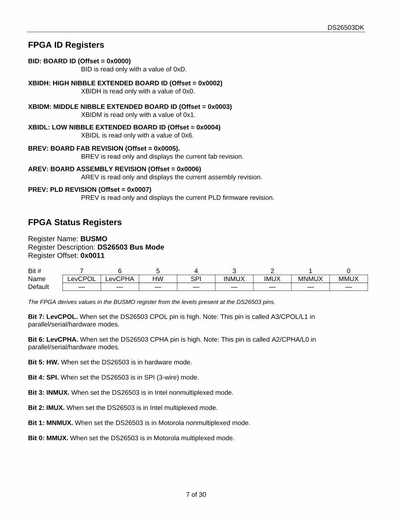
FPGA Status Registers Register Name: BUSMO Register Description: DS26503 Bus Mode Register Offset: 0x0011 Bit # 7 6 5 4 3 2 1 0 Name LevCPOL LevCPHA HW SPI INMUX IMUX MNMUX MMUX Default — — — — — — — — The FPGA derives values in the BUSMO register from the levels present at the DS26503 pins. Bit 7: LevCPOL. When set the DS26503 CPOL pin is high. Note: This pin is called A3/CPOL/L1 in parallel/serial/hardware modes. Bit 6: LevCPHA. When set the DS26503 CPHA pin is high. Note: This pin is called A2/CPHA/L0 in parallel/serial/hardware modes. Bit 5: HW. When set the DS26503 is in hardware mode. Bit 4: SPI. When set the DS26503 is in SPI (3-wire) mode. Bit 3: INMUX. When set the DS26503 is in Intel nonmultiplexed mode. Bit 2: IMUX. When set the DS26503 is in Intel multiplexed mode. Bit 1: MNMUX. When set the DS26503 is in Motorola nonmultiplexed mode. Bit 0: MMUX. When set the DS26503 is in Motorola multiplexed mode.
DS26503DK
8 of 30
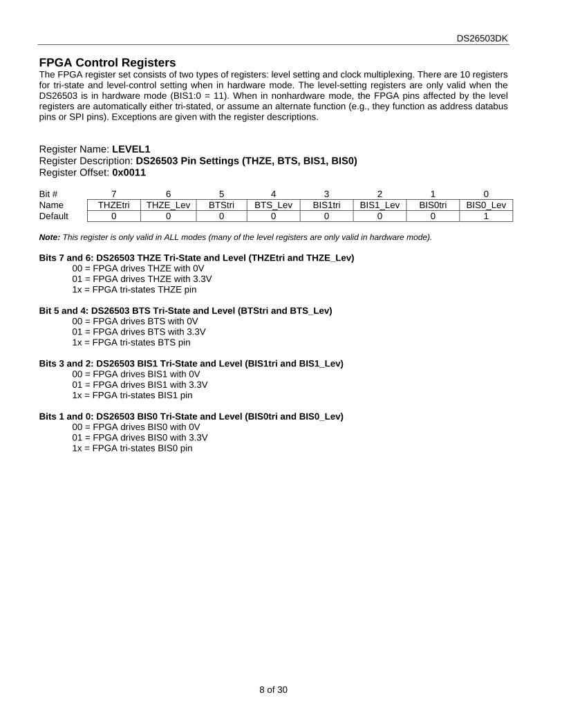
FPGA Control Registers The FPGA register set consists of two types of registers: level setting and clock multiplexing. There are 10 registers for tri-state and level-control setting when in hardware mode. The level-setting registers are only valid when the DS26503 is in hardware mode (BIS1:0 = 11). When in nonhardware mode, the FPGA pins affected by the level registers are automatically either tri-stated, or assume an alternate function (e.g., they function as address databus pins or SPI pins). Exceptions are given with the register descriptions. Register Name: LEVEL1 Register Description: DS26503 Pin Settings (THZE, BTS, BIS1, BIS0) Register Offset: 0x0011 Bit # 7 6 5 4 3 2 1 0 Name THZEtri THZE_Lev BTStri BTS_Lev BIS1tri BIS1_Lev BIS0tri BIS0_Lev Default 0 0 0 0 0 0 0 1 Note: This register is only valid in ALL modes (many of the level registers are only valid in hardware mode). Bits 7 and 6: DS26503 THZE Tri-State and Level (THZEtri and THZE_Lev)
00 = FPGA drives THZE with 0V 01 = FPGA drives THZE with 3.3V 1x = FPGA tri-states THZE pin
Bit 5 and 4: DS26503 BTS Tri-State and Level (BTStri and BTS_Lev)
00 = FPGA drives BTS with 0V 01 = FPGA drives BTS with 3.3V 1x = FPGA tri-states BTS pin
Bits 3 and 2: DS26503 BIS1 Tri-State and Level (BIS1tri and BIS1_Lev)
00 = FPGA drives BIS1 with 0V 01 = FPGA drives BIS1 with 3.3V 1x = FPGA tri-states BIS1 pin
Bits 1 and 0: DS26503 BIS0 Tri-State and Level (BIS0tri and BIS0_Lev)
00 = FPGA drives BIS0 with 0V 01 = FPGA drives BIS0 with 3.3V 1x = FPGA tri-states BIS0 pin
DS26503DK
9 of 30
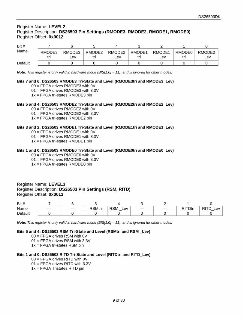
Register Name: LEVEL2 Register Description: DS26503 Pin Settings (RMODE3, RMODE2, RMODE1, RMODE0) Register Offset: 0x0012 Bit # 7 6 5 4 3 2 1 0 Name RMODE3
tri RMODE3
_Lev RMODE2
tri RMODE2
_Lev RMODE1
tri RMODE1
_Lev RMODE0
tri RMODE0
_Lev Default 0 0 0 0 0 0 0 0 Note: This register is only valid in hardware mode (BIS[1:0] = 11), and is ignored for other modes. Bits 7 and 6: DS26503 RMODE3 Tri-State and Level (RMODE3tri and RMODE3_Lev)
00 = FPGA drives RMODE3 with 0V 01 = FPGA drives RMODE3 with 3.3V 1x = FPGA tri-states RMODE3 pin
Bits 5 and 4: DS26503 RMODE2 Tri-State and Level (RMODE2tri and RMODE2_Lev)
00 = FPGA drives RMODE2 with 0V 01 = FPGA drives RMODE2 with 3.3V 1x = FPGA tri-states RMODE2 pin
Bits 3 and 2: DS26503 RMODE1 Tri-State and Level (RMODE1tri and RMODE1_Lev)
00 = FPGA drives RMODE1 with 0V 01 = FPGA drives RMODE1 with 3.3V 1x = FPGA tri-states RMODE1 pin
Bits 1 and 0: DS26503 RMODE0 Tri-State and Level (RMODE0tri and RMODE0_Lev)
00 = FPGA drives RMODE0 with 0V 01 = FPGA drives RMODE0 with 3.3V 1x = FPGA tri-states RMODE0 pin
Register Name: LEVEL3 Register Description: DS26503 Pin Settings (RSM, RITD) Register Offset: 0x0013 Bit # 7 6 5 4 3 2 1 0 Name — — RSMtri RSM _Lev — — RITDtri RITD_Lev Default 0 0 0 0 0 0 0 0 Note: This register is only valid in hardware mode (BIS[1:0] = 11), and is ignored for other modes. Bits 5 and 4: DS26503 RSM Tri-State and Level (RSMtri and RSM _Lev)
00 = FPGA drives RSM with 0V 01 = FPGA drives RSM with 3.3V 1x = FPGA tri-states RSM pin
Bits 1 and 0: DS26503 RITD Tri-State and Level (RITDtri and RITD_Lev)
00 = FPGA drives RITD with 0V 01 = FPGA drives RITD with 3.3V 1x = FPGA Tristates RITD pin
DS26503DK
10 of 30
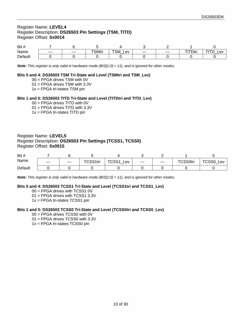
Register Name: LEVEL4 Register Description: DS26503 Pin Settings (TSM, TITD) Register Offset: 0x0014 Bit # 7 6 5 4 3 2 1 0 Name — — TSMtri TSM_Lev — — TITDtri TITD_Lev Default 0 0 0 0 0 0 0 0 Note: This register is only valid in hardware mode (BIS[1:0] = 11), and is ignored for other modes. Bits 5 and 4: DS26503 TSM Tri-State and Level (TSMtri and TSM_Lev)
00 = FPGA drives TSM with 0V 01 = FPGA drives TSM with 3.3V 1x = FPGA tri-states TSM pin
Bits 1 and 0: DS26503 TITD Tri-State and Level (TITDtri and TITD_Lev)
00 = FPGA drives TITD with 0V 01 = FPGA drives TITD with 3.3V 1x = FPGA tri-states TITD pin
Register Name: LEVEL5 Register Description: DS26503 Pin Settings (TCSS1, TCSS0) Register Offset: 0x0015 Bit # 7 6 5 4 3 2 1 0 Name — — TCSS1tri TCSS1_Lev — — TCSS0tri TCSS0_Lev Default 0 0 0 0 0 0 0 0 Note: This register is only valid in hardware mode (BIS[1:0] = 11), and is ignored for other modes. Bits 5 and 4: DS26503 TCSS1 Tri-State and Level (TCSS1tri and TCSS1_Lev)
00 = FPGA drives with TCSS1 0V 01 = FPGA drives with TCSS1 3.3V 1x = FPGA tri-states TCSS1 pin
Bits 1 and 0: DS26503 TCSS0 Tri-State and Level (TCSS0tri and TCSS0_Lev)
00 = FPGA drives TCSS0 with 0V 01 = FPGA drives TCSS0 with 3.3V 1x = FPGA tri-states TCSS0 pin
DS26503DK
11 of 30
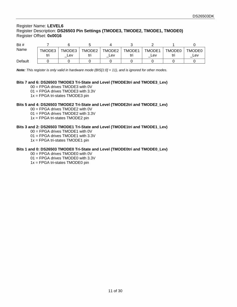
Register Name: LEVEL6 Register Description: DS26503 Pin Settings (TMODE3, TMODE2, TMODE1, TMODE0) Register Offset: 0x0016 Bit # 7 6 5 4 3 2 1 0 Name TMODE3
tri TMODE3
_Lev TMODE2
tri TMODE2
_Lev TMODE1
tri TMODE1
_Lev TMODE0
tri TMODE0
_Lev Default 0 0 0 0 0 0 0 0 Note: This register is only valid in hardware mode (BIS[1:0] = 11), and is ignored for other modes. Bits 7 and 6: DS26503 TMODE3 Tri-State and Level (TMODE3tri and TMODE3_Lev)
00 = FPGA drives TMODE3 with 0V 01 = FPGA drives TMODE3 with 3.3V 1x = FPGA tri-states TMODE3 pin
Bits 5 and 4: DS26503 TMODE2 Tri-State and Level (TMODE2tri and TMODE2_Lev)
00 = FPGA drives TMODE2 with 0V 01 = FPGA drives TMODE2 with 3.3V 1x = FPGA tri-states TMODE2 pin
Bits 3 and 2: DS26503 TMODE1 Tri-State and Level (TMODE1tri and TMODE1_Lev)
00 = FPGA drives TMODE1 with 0V 01 = FPGA drives TMODE1 with 3.3V 1x = FPGA tri-states TMODE1 pin
Bits 1 and 0: DS26503 TMODE0 Tri-State and Level (TMODE0tri and TMODE0_Lev)
00 = FPGA drives TMODE0 with 0V 01 = FPGA drives TMODE0 with 3.3V 1x = FPGA tri-states TMODE0 pin
DS26503DK
12 of 30
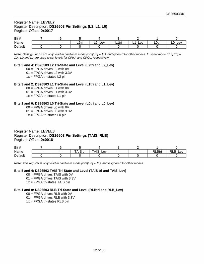
Register Name: LEVEL7 Register Description: DS26503 Pin Settings (L2, L1, L0) Register Offset: 0x0017 Bit # 7 6 5 4 3 2 1 0 Name — — L2tri L2_Lev L1tri L1_Lev L0tri L0_Lev Default 0 0 0 0 0 0 0 0 Note: Settings for L2 are only valid in hardware mode (BIS[1:0] = 11), and ignored for other modes. In serial mode (BIS[1:0] = 10), L0 and L1 are used to set levels for CPHA and CPOL, respectively. Bits 5 and 4: DS26503 L2 Tri-State and Level (L2tri and L2_Lev)
00 = FPGA drives L2 with 0V 01 = FPGA drives L2 with 3.3V 1x = FPGA tri-states L2 pin
Bits 3 and 2: DS26503 L1 Tri-State and Level (L1tri and L1_Lev)
00 = FPGA drives L1 with 0V 01 = FPGA drives L1 with 3.3V 1x = FPGA tri-states L1 pin
Bits 1 and 0: DS26503 L0 Tri-State and Level (L0tri and L0_Lev)
00 = FPGA drives L0 with 0V 01 = FPGA drives L0 with 3.3V 1x = FPGA tri-states L0 pin
Register Name: LEVEL8 Register Description: DS26503 Pin Settings (TAIS, RLB) Register Offset: 0x0018 Bit # 7 6 5 4 3 2 1 0 Name — — TAIS tri TAIS_Lev — — RLBtri RLB_Lev Default 0 0 0 0 0 0 0 0 Note: This register is only valid in hardware mode (BIS[1:0] = 11), and is ignored for other modes. Bits 5 and 4: DS26503 TAIS Tri-State and Level (TAIS tri and TAIS_Lev)
00 = FPGA drives TAIS with 0V 01 = FPGA drives TAIS with 3.3V 1x = FPGA tri-states TAIS pin
Bits 1 and 0: DS26503 RLB Tri-State and Level (RLBtri and RLB_Lev) 00 = FPGA drives RLB with 0V 01 = FPGA drives RLB with 3.3V 1x = FPGA tri-states RLB pin
DS26503DK
13 of 30
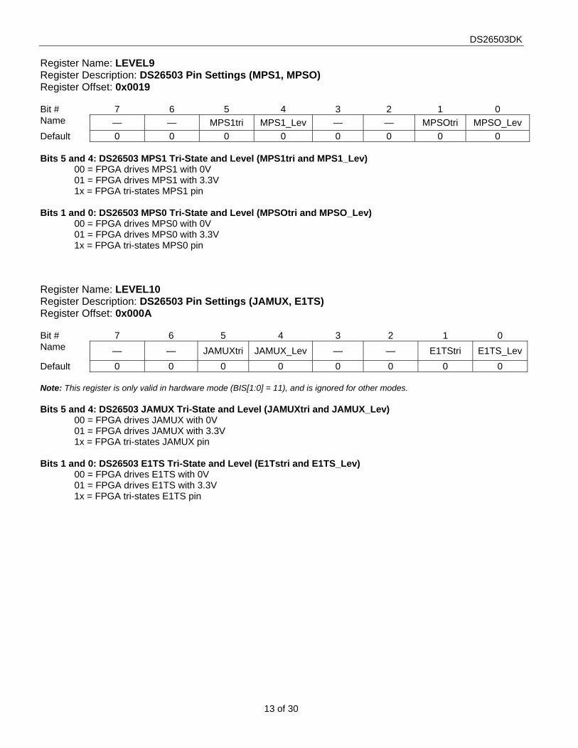
Register Name: LEVEL9 Register Description: DS26503 Pin Settings (MPS1, MPSO) Register Offset: 0x0019 Bit # 7 6 5 4 3 2 1 0 Name — — MPS1tri MPS1_Lev — — MPSOtri MPSO_Lev Default 0 0 0 0 0 0 0 0 Bits 5 and 4: DS26503 MPS1 Tri-State and Level (MPS1tri and MPS1_Lev)
00 = FPGA drives MPS1 with 0V 01 = FPGA drives MPS1 with 3.3V 1x = FPGA tri-states MPS1 pin
Bits 1 and 0: DS26503 MPS0 Tri-State and Level (MPSOtri and MPSO_Lev)
00 = FPGA drives MPS0 with 0V 01 = FPGA drives MPS0 with 3.3V 1x = FPGA tri-states MPS0 pin
Register Name: LEVEL10 Register Description: DS26503 Pin Settings (JAMUX, E1TS) Register Offset: 0x000A Bit # 7 6 5 4 3 2 1 0 Name — — JAMUXtri JAMUX_Lev — — E1TStri E1TS_LevDefault 0 0 0 0 0 0 0 0 Note: This register is only valid in hardware mode (BIS[1:0] = 11), and is ignored for other modes. Bits 5 and 4: DS26503 JAMUX Tri-State and Level (JAMUXtri and JAMUX_Lev)
00 = FPGA drives JAMUX with 0V 01 = FPGA drives JAMUX with 3.3V 1x = FPGA tri-states JAMUX pin
Bits 1 and 0: DS26503 E1TS Tri-State and Level (E1Tstri and E1TS_Lev)
00 = FPGA drives E1TS with 0V 01 = FPGA drives E1TS with 3.3V 1x = FPGA tri-states E1TS pin
DS26503DK
14 of 30
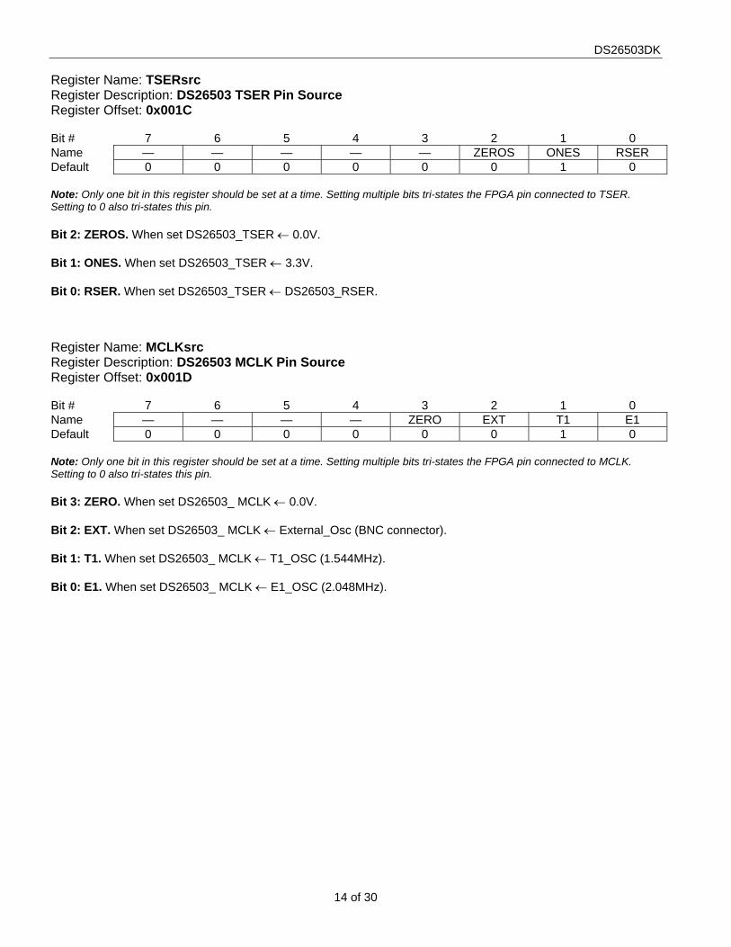
Register Name: TSERsrc Register Description: DS26503 TSER Pin Source Register Offset: 0x001C Bit # 7 6 5 4 3 2 1 0 Name — — — — — ZEROS ONES RSER Default 0 0 0 0 0 0 1 0 Note: Only one bit in this register should be set at a time. Setting multiple bits tri-states the FPGA pin connected to TSER. Setting to 0 also tri-states this pin. Bit 2: ZEROS. When set DS26503_TSER ← 0.0V. Bit 1: ONES. When set DS26503_TSER ← 3.3V. Bit 0: RSER. When set DS26503_TSER ← DS26503_RSER. Register Name: MCLKsrc Register Description: DS26503 MCLK Pin Source Register Offset: 0x001D Bit # 7 6 5 4 3 2 1 0 Name — — — — ZERO EXT T1 E1 Default 0 0 0 0 0 0 1 0 Note: Only one bit in this register should be set at a time. Setting multiple bits tri-states the FPGA pin connected to MCLK. Setting to 0 also tri-states this pin. Bit 3: ZERO. When set DS26503_ MCLK ← 0.0V. Bit 2: EXT. When set DS26503_ MCLK ← External_Osc (BNC connector). Bit 1: T1. When set DS26503_ MCLK ← T1_OSC (1.544MHz). Bit 0: E1. When set DS26503_ MCLK ← E1_OSC (2.048MHz).
DS26503DK
15 of 30
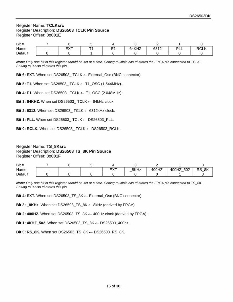
Register Name: TCLKsrc Register Description: DS26503 TCLK Pin Source Register Offset: 0x001E Bit # 7 6 5 4 3 2 1 0 Name — EXT T1 E1 64KHZ 6312 PLL RCLK Default 0 0 1 0 0 0 0 0 Note: Only one bit in this register should be set at a time. Setting multiple bits tri-states the FPGA pin connected to TCLK. Setting to 0 also tri-states this pin. Bit 6: EXT. When set DS26503_ TCLK ← External_Osc (BNC connector). Bit 5: T1. When set DS26503_ TCLK ← T1_OSC (1.544MHz). Bit 4: E1. When set DS26503_ TCLK ← E1_OSC (2.048MHz). Bit 3: 64KHZ. When set DS26503_ TCLK ← 64kHz clock. Bit 2: 6312. When set DS26503_ TCLK ← 6312kHz clock. Bit 1: PLL. When set DS26503_ TCLK ← DS26503_PLL. Bit 0: RCLK. When set DS26503_ TCLK ← DS26503_RCLK. Register Name: TS_8Ksrc Register Description: DS26503 TS_8K Pin Source Register Offset: 0x001F Bit # 7 6 5 4 3 2 1 0 Name — — — EXT _8KHz 400HZ 400HZ_502 RS_8K Default 0 0 0 0 0 0 1 0 Note: Only one bit in this register should be set at a time. Setting multiple bits tri-states the FPGA pin connected to TS_8K. Setting to 0 also tri-states this pin. Bit 4: EXT. When set DS26503_TS_8K ← External_Osc (BNC connector). Bit 3: _8KHz. When set DS26503_TS_8K ← 8kHz (derived by FPGA). Bit 2: 400HZ. When set DS26503_TS_8K ← 400Hz clock (derived by FPGA). Bit 1: 4KHZ_502. When set DS26503_TS_8K ← DS26503_400hz. Bit 0: RS_8K. When set DS26503_TS_8K ← DS26503_RS_8K.
DS26503DK
16 of 30
Maxim/Dallas Semiconductor cannot assume responsibility for use of any circuitry other than circuitry entirely embodied in a Maxim/Dallas Semiconductor product. No circuit patent licenses are implied. Maxim/Dallas Semiconductor reserves the right to change the circuitry and specifications without notice at any time. Maxim Integrated Products , 120 San Gabrie l Dr ive , Sunnyvale , CA 94086 408-737-7600
© 2006 Maxim Integrated Products The Maxim logo is a registered trademark of Maxim Integrated Products, Inc. The Dallas logo is a registered trademark of Dallas Semiconductor Corporation.
DS26503 INFORMATION For more information about the DS26503, consult the DS26503 data sheet available on our website at www.maxim-ic.com/DS26503. Software downloads are also available for this design kit. DS26503DK INFORMATION For more information about the DS26503DK, including software downloads, consult the DS26503DK data sheet available on our website at www.maxim-ic.com/DS26503DK. TECHNICAL SUPPORT For additional technical support, go to www.maxim-ic.com/support.
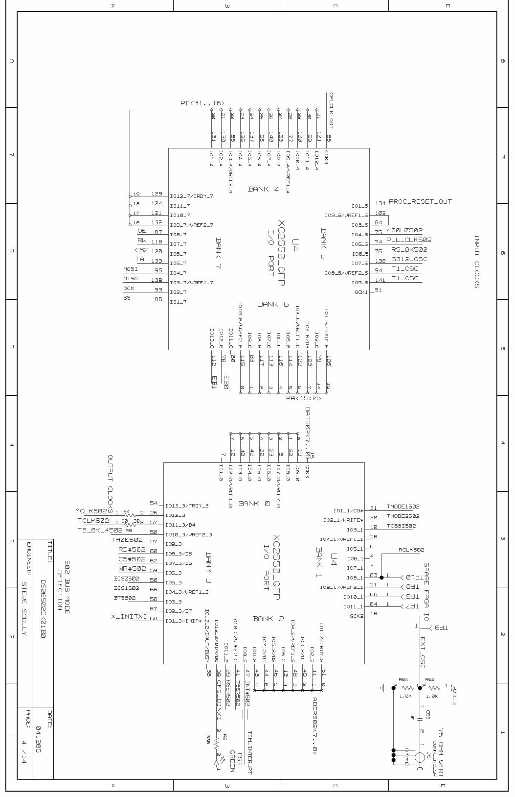
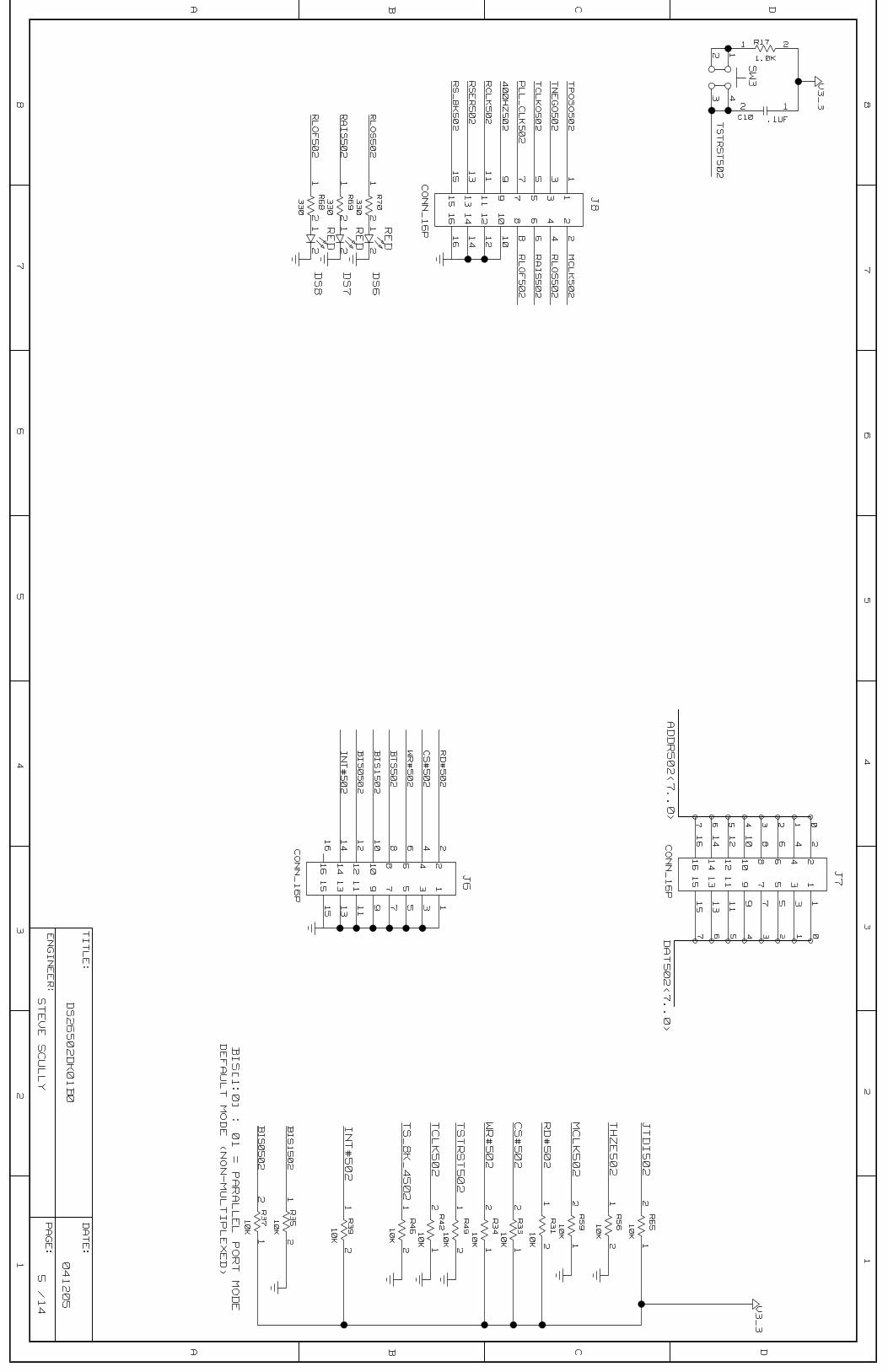
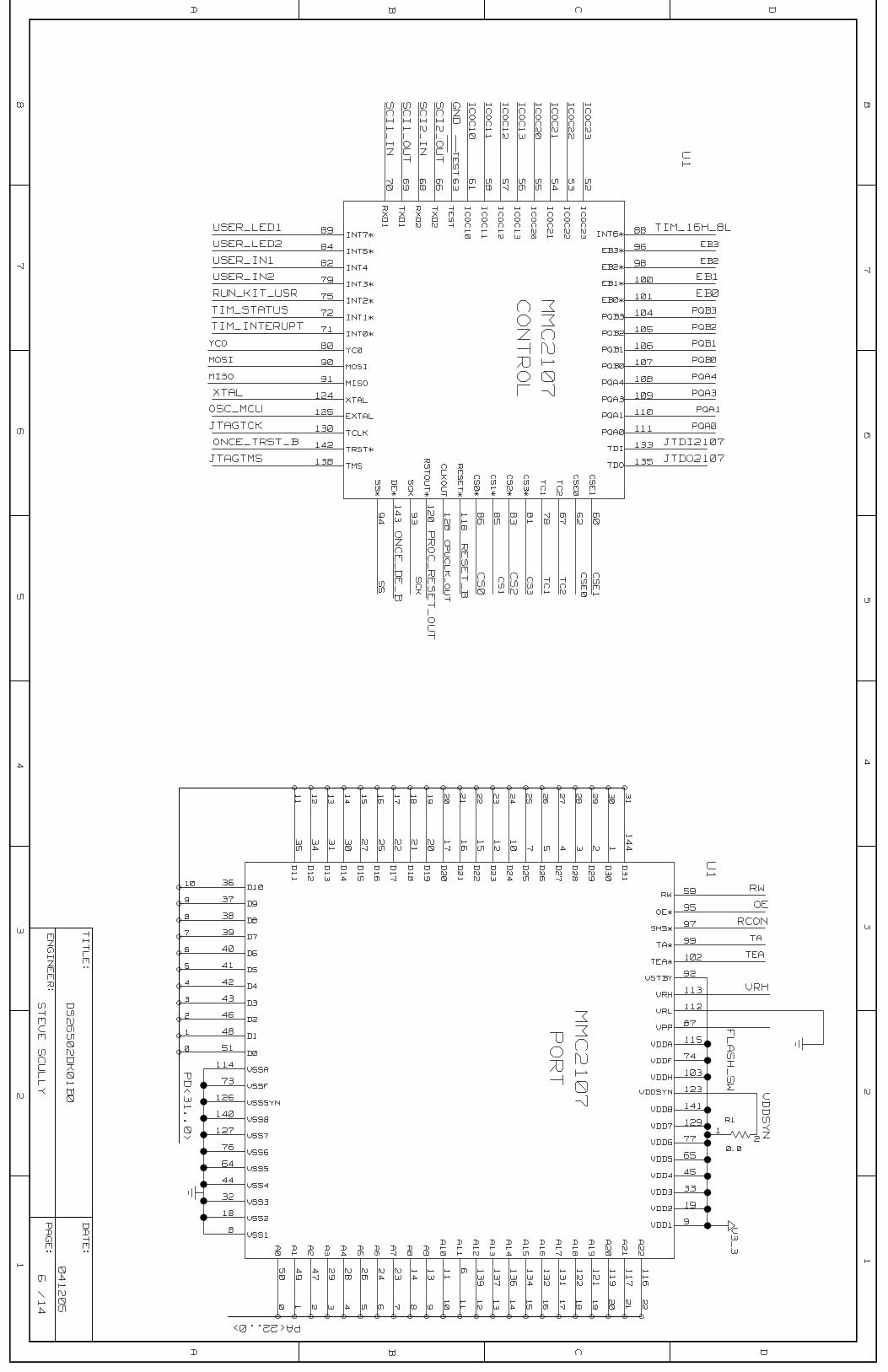
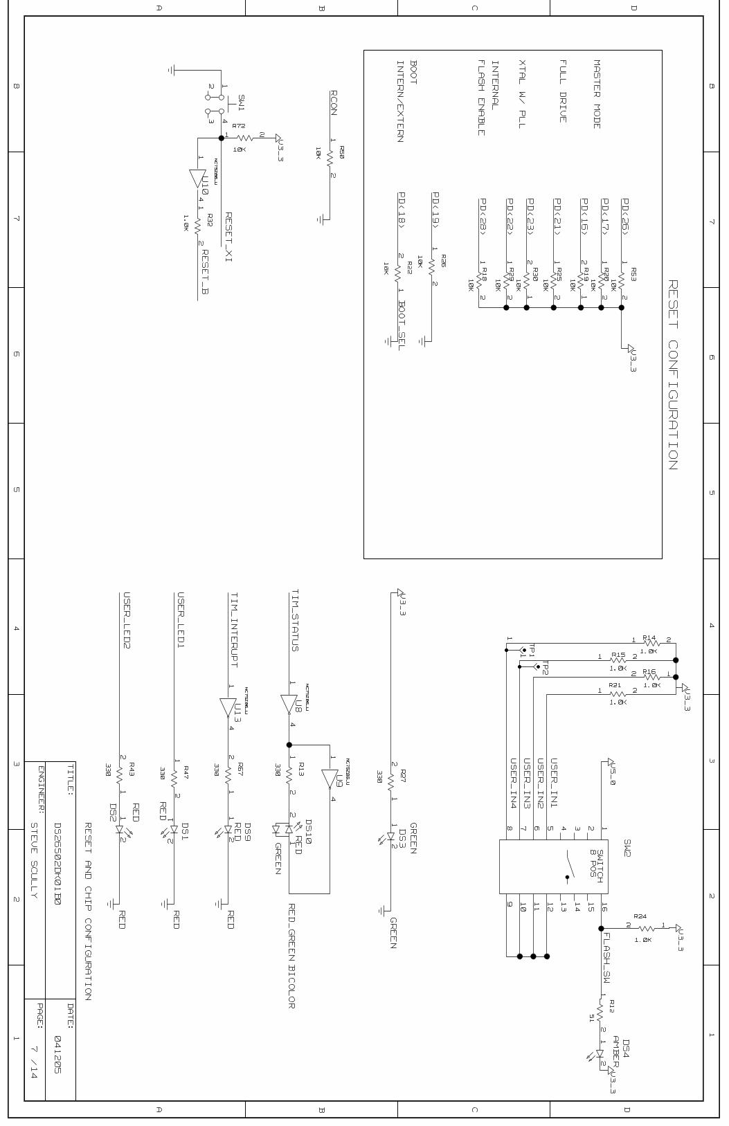
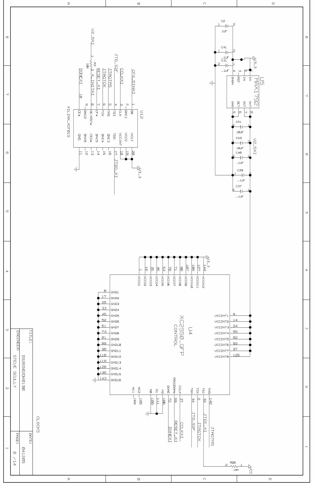
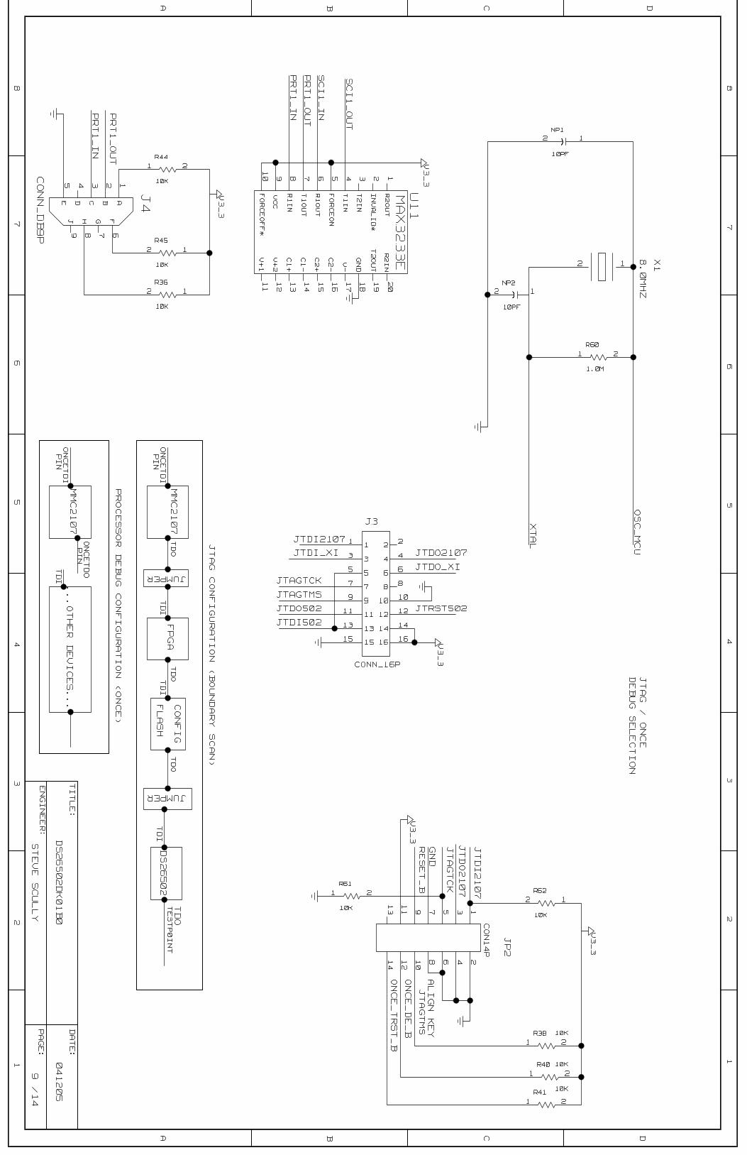
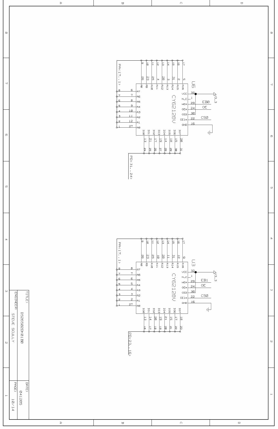
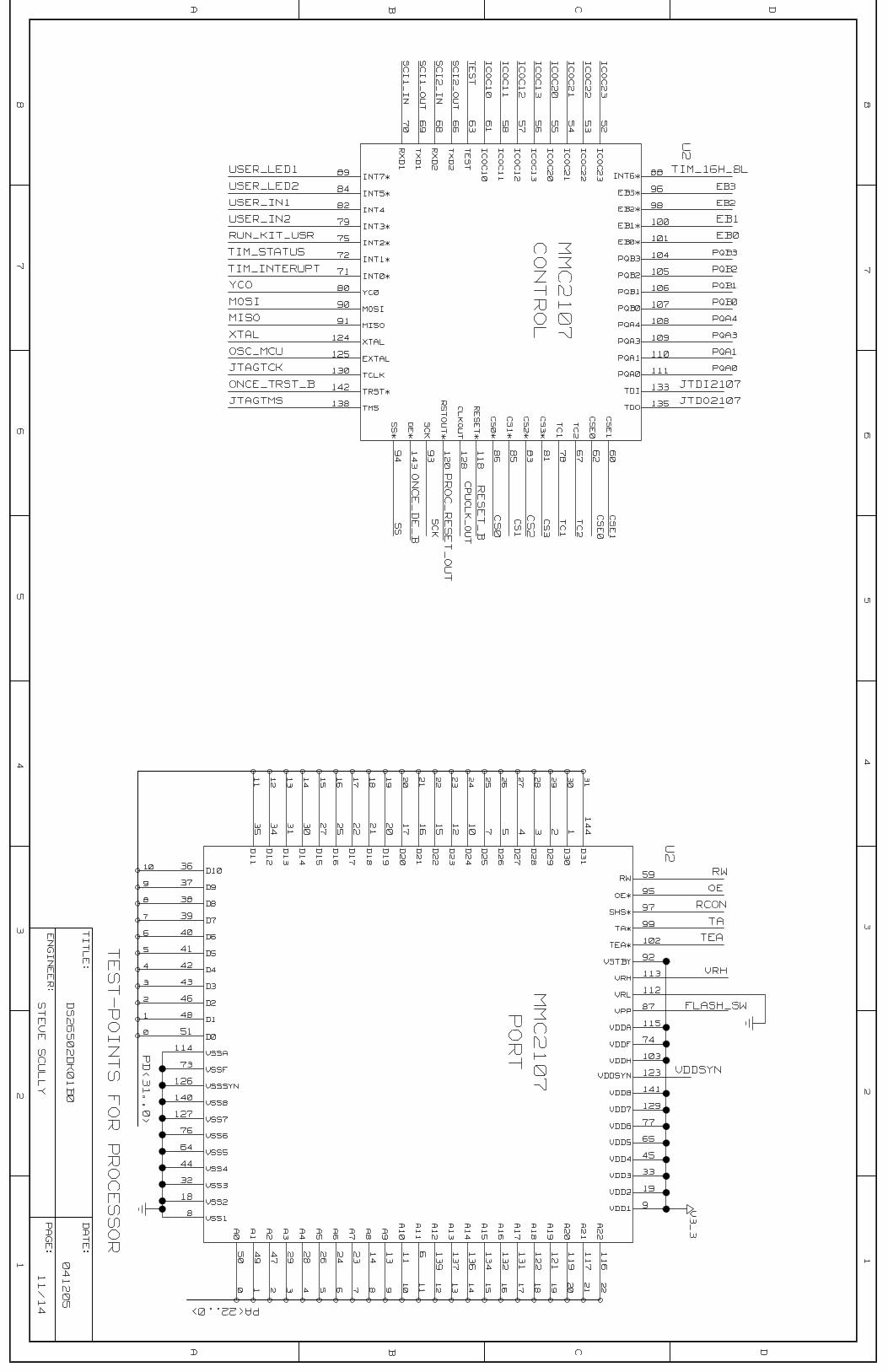
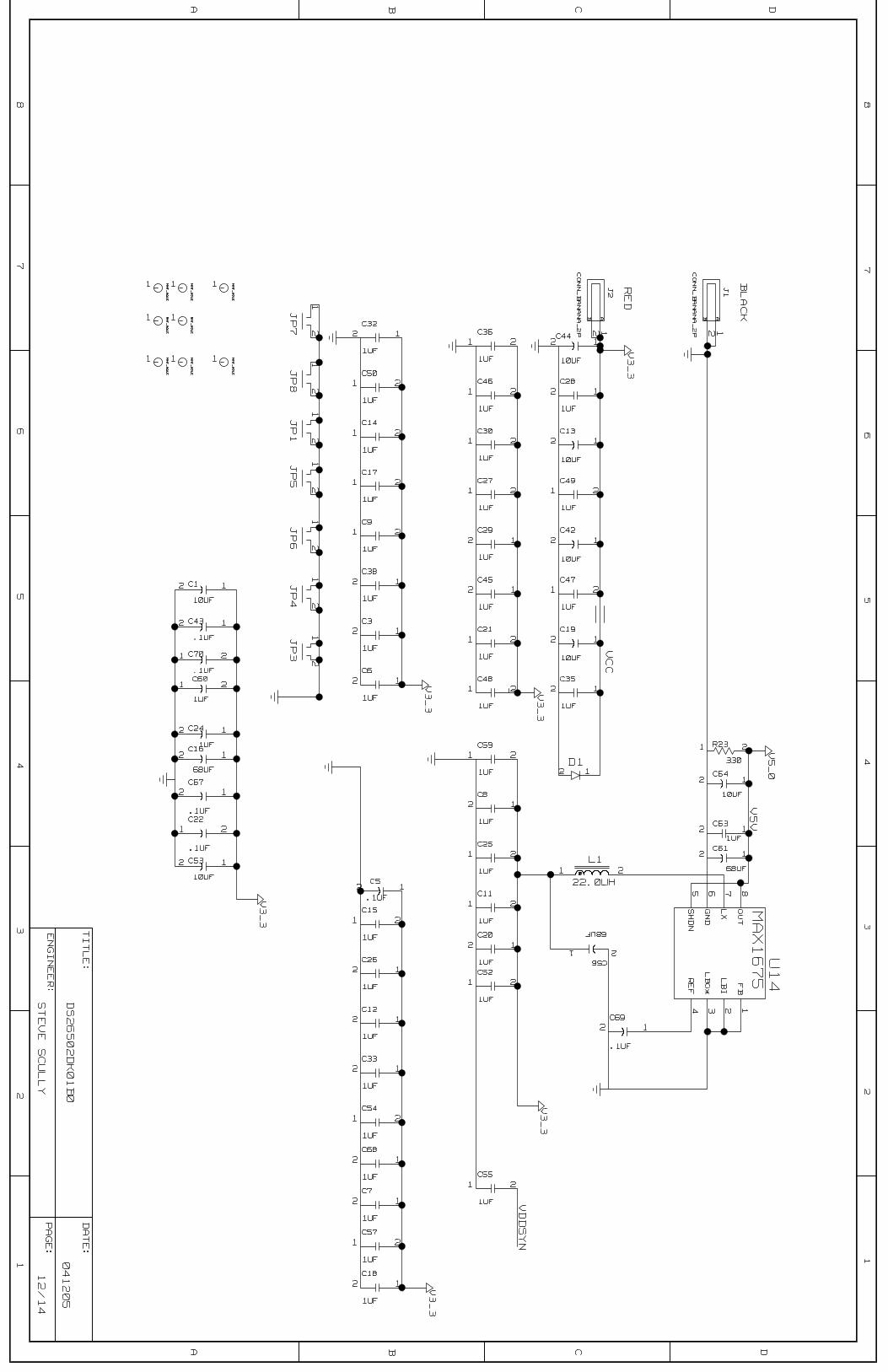
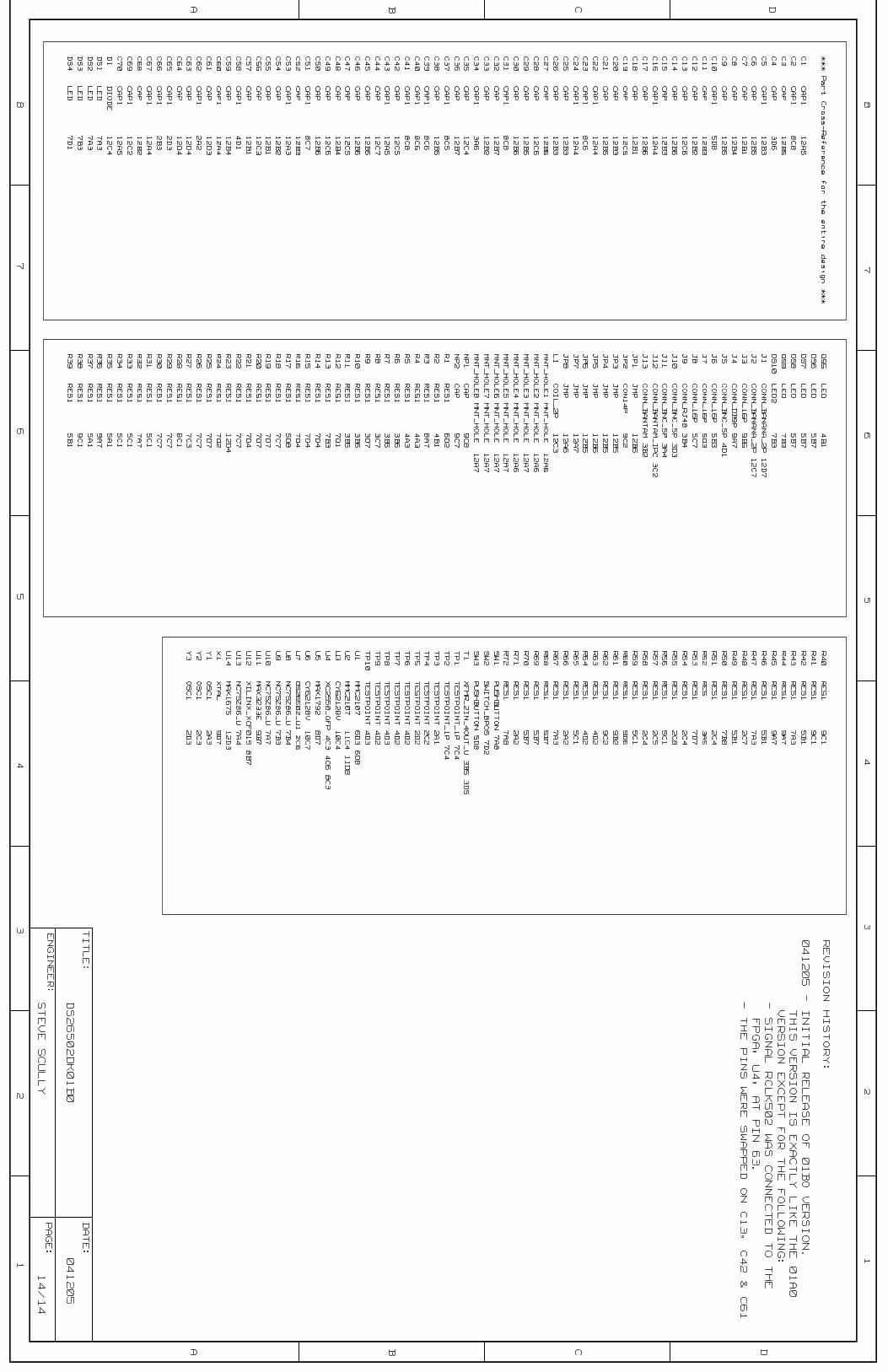
SCHEMATICS The DS26503DK schematics are featured in the following pages.
DOCUMENT REVISION HISTORY REVISION
DATE DESCRIPTION
110205 Initial DS26503DK data sheet release.
071006 Updated descriptions for FPGA Control Registers LEVEL1 to LEVEL10.
110106 Updated schematics.
031507 Corrected typo on Bit 0 of TSERsrc register Corrected typo on Bit 0 of TS_8Ksrc register
CONVERTED
TO
PDF:
DESIGN
KIT
DS26502
/
DS26502DK01B0
STEVE
SCULLY
3.
DS26502LINE
BUILD
OUT
5.
TESTPOINTSFORDS26502
7.
PROCESSORCONFIGURATION
8.
XILINXCONFIGURATIONANDCOREVOLTAGE
11.
PROCESSORTEST
POINTS
12.
FLASH
VOLTAGEAND
DECOUPLING
13.
SIGNALCROSS
REFERENCE
14.PARTCROSSREFERENCEANDREVISIONHISTORY
10.
MEMORY
9.
SERIALPORTSANDJTAGCONFIGURATION
6.
MMC2107PROCESSOR
4.
XILINXCLOCKMUXANDBUSCONVERSION
2.
DS26502ANDOSCILLATORS
1.
CONTENTS
041205
114
FriOct20
10:08:322006
PAGE:
DATE:
TITLE:
ENGINEER:
AA
BB
CC
DD
1 122
3 344
5 566
7 788
/
DS26502DK01B0
STEVE
SCULLY
041205
214
1
TP3
1 TP4
1 TP5
81
54
Y1
2 1C66
81
54
Y2
2 1C65
81
54
Y3
21
C62
21R71
12R66
62
5253
51
39
21
23
54
20
19
48
49
50
31
18
17
45
43
40
38
41
28
26
42
32
30
61
25
29
47
44
35
33
37
36
34
46
22
8
56
24
7
58
60
55
59
57
6 5 4 3 2 1 64
63
16
15
14
13
12
1110
9
27
U7
2R55
1R48
1R57
21
R51
12
R58
1R54
1UF
ADDR502<7..0>
CS#502
TSTRST502
1
MCLK502
RRING502
E1_OSC
T1_OSC
TNEGO502
TPOSO502
RLOF502
RLOS502
JTDO502
TCLKO502
6312_OSC
1.0K
TRING502
TTIP502
RAIS502
RD#502
BTS502
BIS1502
WR#502
INT#502
THZE502
BIS0502
400HZ502
PLL_CLK502
DAT502<7..0>
RSER502
RCLK502
7 6 5 4 3
30
30
12 0 7 56 4 23 0
1.544MHZ_3.3V
.1UF.1UF
1.0K
2.048MHZ_3.3V
JTRST502
JTDI502
JTAGTMS
JTAGTCK
6312
KHZ__3.3V
RTIP502
TSER502
TS_8K_4502
TCSSI502
TMODE2502
TMODE1502
TCLK502
RS_8K502
PAGE:
DATE:
TITLE:
ENGINEER:
AA
BB
CC
DD
1 122
3 344
5 566
7 788
V3_3
VCC
1
OSC
GND
OUT
VCC
1
OSC
GND
OUT
V3_3
VCC
1
OSC
GND
OUT
V3_3
V3_3
V3_3
V3_3
V3_3
DS26502
THZE
BIS0
BIS1
MCLK
-/-/TCSSI
RS_8K
400HZ
TSTRST
DVDD3
INT*/INT*/JACKS
RVSS1
TVSS
RVSS3
RVSS2
DVSS1
DVSS2
DVSS3
RVDD
JTDO
JTRST
JTDI
JTCLK
JTMS
TSER
TCLK
RRING
RAIS
RLOS
RLOF_CCE
TPOSO
TNEGO
RSER
RCLK
PLL_OUT
TCLKO
AD<7>/-/RITD
AD<6>/-/TITD
AD<4>/-/RMODE0
AD<5>/-/RMODE1
AD<3>/-/TSM
AD<1>/MOSI/RMODE3
AD<2>/SCLK/RSM
AD<0>/MISO/TCSS0
ALE(AS)/A<7>/-/MPS1
A<6>/-/MPS0
A<5>/CPOL/TMODE0
A<4>/CPHA/L2
A<3>/-/L1
A<2>/-/L0
A<1>/-/TAIS
A<0>/-/EITS
TTIP
TRING
RTIP
BTS/-/HBE
WR*(R/W*)/-/TMODE3
CS*/CS*/RLB
RD*(DS*)/-/RMODE2
DVDD2
DVDD1
TVDD
-/-/TMODE1
-/-/TMODE2
TS_8K_4

/
THE
SCHEMATICHAS
BEEN
UPDATEDAND
IS
CORRECT.
REMOVEDSINCE
IT
HAS
NON-STANDARDCONNECTION.
(REFERENCEDESIGNATORJ9).
THERJ48CONNECTORSHOULDBE
DO
NOTUSETHECORRECTPINNUMBERSON
THERJ48CONNECTOR
NOTE:
BOARDREVISIONSDS26502DK01A0ANDDS26502DK01B0
ON
THEDS26502DK01B0CIRCUITBOARDS
ON
THETTIPPIN.
THISHASBEENINCREASEDTO
10UF
1UFCAPACITOR(REFERENCEDESIGNATORC4)FORDC
BLOCKING
NOTE:
THEDS26502DK01A0CIRCUITBOARDSUSEDA
STEVE
SCULLY
14
041205
3
DS26502DK01B0
61.9
RRING502
RTIP502
TRING502
0.0
75
OHM
RA
0.0
61.9
0.0
51.1
75
OHM
RA
0.0
.1UF
10UF
J12
52
J10
2345
1
J13
52
J11
2345
1
109
7856
T1
14
15
16
3 4 1 2
R52
1 2
R9
12
R8
12
R6
21
C3412
R7
21
R10
12
R11
12
J9
1
2
3
4
6
5
7
8
TTIP502
T1
11
C4
PAGE:
DATE:
TITLE:
ENGINEER:
AA
BB
CC
DD
1 122
3 344
5 566
7 788
1:1
1:0.8
1:1
1:0.8
CONN_BNC_5P
CONN_BANTAM
T R
CONN_RJ48
E
HF
C
B
G
D
A
CONN_BNC_5P
CONN_BANTAM_IPC
RT
OUTPUTCLOCKS
502
BUS
MODE
/
DETECTION
INPUT
CLOCKS
SPARE
FPGA
IO
DS26502DK01B0
STEVE
SCULLY
4
041205
14
1
TP9
21 R4
21
R5
1
5432 J
5
12
C58
12R63
12R64
132
83
141
77
87
117
94
103
118113
138
140
120
116
7696
133
114
74
137
95
122
75
136
139
123
84
85
93
79
102
130
86
126
134
131
112
129
78
101
124
80
99
121
115
100
91
88
U4
1
TP10
1
TP8
27
47
21
19
60
43
63
20
62
44
3
5
59
46
4
23
50
13
6
22
65
48
28
42
56
49
10
40
67
11
30
12
68
51
31
7
54
38
26
39
57
29
64
58
41
66
15
18
U4
1
TP6
1
TP7
12
R2
21
DS5
7
OE
75
OHM
VERT
TIM_INTERUPT
GREEN
WR#502
THZE502
TS_8K_4502
MCLK502
MOSI
E1_OSC
T1_OSC
PROC_RESET_OUT
400HZ502
PLL_CLK502
RS_8K502
CPUCLK_OUT
EB0
EB1
X_INITXI
15
PD<31..16>
DAT502<7..0>
BIS1502
BIS0502
6312_OSC
SS
SCK
MISO
TACS2
RW
20
21
22
23
24
25
26
27
28
29
30
19
18
17
31
16
0 1 3 4 5 6 7
14
6 5 4 3 2 1 0
6 5 4 3 2
330
01
2
BTS502
PA<15:0>
PD<31..16>
ADDR502<7..0>
1.0K
RD#502
CS#502
3030TCLK502
1.0K
1UF
7
INT#502
TSER502
RSER502
CFG_DINXI
EXT_OSC
TMODE2502
TMODE1502
TCSSI502
RCLK502
PAGE:
DATE:
TITLE:
ENGINEER:
AA
BB
CC
DD
1 122
3 344
5 566
7 788
CONN_BNC_5P
V3_3
I/O
PORT
BANK 4
BANK
7BANK 6
BANK
5
XC2S50_QFP
IO1_5
IO2_5/VREF1_5
IO3_5
IO4_5
IO5_5
IO6_5
IO7_5
IO8_5/VREF2_5
IO9_5
GCK1
IO13_6
IO12_6
IO11_6
IO10_6/VREF2_6
IO9_6
IO8_6
IO7_6
IO6_6
IO5_6
IO4_6/VREF1_6
IO3_6/D3
IO2_6
IO1_6/TRDY_6
IO1_7
IO2_7
IO3_7/VREF1_7
IO4_7
IO5_7
IO6_7
IO7_7
IO8_7
IO9_7/VREF2_7
IO10_7
IO11_7
IO12_7/IRDY_7
IO1_4
IO2_4
IO3_4/VREF2_4
IO4_4
IO5_4
IO6_4
IO7_4
IO8_4
IO9_4/VREF1_4
IO10_4
IO11_4
IO12_4
GCK0
XC2S50_QFP
I/O
PORT
BANK
3
BANK 2
BANK
1
BANK 0
IO6_1
IO5_1
IO4_1/VREF1_1
IO3_1
IO2_1/WRITE*
IO1_1/CS*
IO7_1
IO8_1
IO9_1/VREF2_1
IO10_1
IO11_1
GCK2
IO13_2/DOUT/BUSY
IO12_2/DIN/D0
IO11_2
IO10_2/VREF2_2
IO9_2
IO8_2
IO7_2/D1
IO6_2/D2
IO5_2
IO4_2/VREF1_2
IO3_2/D3
IO2_2
IO1_2/IRDY_2
IO1_3/INIT*
IO2_3/D7
IO3_3
IO4_3/VREF1_3
IO5_3
IO6_3
IO7_3/D6
IO8_3/D5
IO9_3
IO10_3/VREF2_3
IO11_3/D4
IO12_3
IO13_3/TRDY_3
IO1_0
IO2_0/VREF1_0
IO3_0
IO4_0
IO5_0
IO6_0
IO7_0/VREF2_0
IO8_0
IO9_0
GCK3
DEFAULTMODE
(NON-MULTIPLEXED)
BIS[1:0]:
01
=PARALLELPORTMODE
/
DS26502DK01B0
STEVE
SCULLY
04120514
5
21
R68
21
R69
21
DS7
21
DS8
21
R70
21
DS6
21 R17
432 1
SW3
2 1C10
16
15
14
13
12
11
10
9
87
65
43
21
J8
16
15
14
13
12
11
10
9
87
65
43
21
J6
16
15
14
13
12
11
10
9
87
65
43
21
J7
12
R37
21
R35
21
R39
21
R46
12
R42
21
R49
12
R34
12
R33
21
R31
12
R59
21
R56
12
R65
RLOF502
JTDI502
RD#502
.1UF
1.0K
TSTRST502
ADDR502<7..0>
RS_8K502
400HZ502
RLOS502
MCLK502
DAT502<7..0>
01235 4
RED
RED
330
RAIS502
BIS0502
BIS1502
TS_8K_4502
TCLK502
TSTRST502
WR#502
CS#502
MCLK502
THZE502
10K
10K 10K
10K
10K
10K
10K
10K
10K
10K
10K
TCLKO502
RSER502
RCLK502
PLL_CLK502
TPOSO502
TNEGO502
RLOF502
0123457
WR#502
BIS0502
BIS1502
BTS502
CS#502
RD#502
330
RLOS502
RAIS502
RED
330
INT#502
10K
INT#502
67
6
PAGE:
DATE:
TITLE:
ENGINEER:
AA
BB
CC
DD
1 122
3 344
5 566
7 788
CONN_16P
248
10
12
14
16
3 17911
13
15
56
V3_3
CONN_16P
24810
12
14
16
3 179
11
13
15 5
6
CONN_16P
24810
12
14
16
3 179
11
13
15 5
6
V3_3
/STEVE
SCULLY
DS26502DK01B0
614
041205
80
124
66
69
142
138
63
135
133
130
67
78
94
93
68
70
120 118
104
105
106
107
108
109
110
111
90
91
89 88
84
82
79
75
72
71
52
53
54
55
56
57
58
61
125
96
98
100
101
143 60
62
81
83
85
86
128
U1
92
126
73
114
140
127
76
64
44
32
18
8
112
113
87
123
103
74
115
141
129
77
65
45
33
19
9
102
99
97
59
9537
38
39
40
41
42
1441
43
23457
10
12
15
16
17
46
20
21
22
25
27
30
31
34
35
36
48
51
13
14
23
24
26
28
29
116
117
119
47
121
122
131
132
134
136
137
139
611
49
50
U1
21
R1
10
XTAL
ONCE_TRST_B
JTAGTMS
TIM_16H_8L
VRH
TEA
TA
RCON
OE
VDDSYN
FLASH_SW
JTDO2107
JTDI2107
PQA0
PQA1
PQA3
PQB0
PQB2
PQB3
EB0
EB1
EB3
JTAGTCK
OSC_MCU
MOSI
YCO
TIM_INTERUPT
TIM_STATUS
RUN_KIT_USR
USER_IN2
USER_IN1
USER_LED2
USER_LED1
ONCE_DE_B
0.0
22
20
21
18
19
16
15
17
13
14
10
11
128 965 72 3 40 1
31
30
29
28
27
25
26
24
23
22
21
20
19
18
17
16
15
0
1
2
3
4
5
7
6
14
13
12
11
8
9
PA<22..0>
PD<31..0>
RW
GND
SCI1_OUT
SCI2_IN
MISO
CS0
RESET_B
CPUCLK_OUT
PROC_RESET_OUT
SCK
CS2
CS1
CSE0
TC2
EB2
PQB1
CSE1
TC1
CS3
PQA4
SS
ICOC22
ICOC23
ICOC20
ICOC21
ICOC11
ICOC12
ICOC13
TEST
ICOC10
SCI2_OUT
SCI1_IN
PAGE:
DATE:
TITLE:
ENGINEER:
AA
BB
CC
DD
1 122
3 344
5 566
7 788
MMC2107
CONTROL
RXD1
INT7*
TXD2
ICOC10
TEST
INT1*
ICOC13
ICOC12
ICOC11
ICOC21
ICOC20
ICOC23
ICOC22
EXTAL
TCLK
TRST*
SS*
PQB0
PQA4
PQA3
PQA0
PQA1
CS3*
TC1
TDI
TDO
CSE1
EB3*
INT6*
PQB1
PQB2
PQB3
EB0*
EB1*
EB2*
TC2
CSE0
CS1*
CS2*
DE*
SCK
RSTOUT*
CLKOUT
RESET*
CS0*
TMS
INT0*
YC0
MOSI
MISO
XTAL
INT3*
INT2*
INT5*
INT4
RXD2
TXD1
MMC2107
PORT
TA*
SHS*
OE*
VRH
VSTBY
TEA*
VDDH
VDDF
VDDA
VPP
VDD6
VDD7
VDD8
VDDSYN
VDD3
VDD5
RW
VRL
A8
D31
A22
A21
A20
A19
A18
A17
A16
A15
A14
A13
A12
A11
A10
A9
A7
A6
A5
A4
A3
A2
A1
A0
VSS1
VSS2
VSS3
VSS4
VSS5
VSS6
VSS7
VSS8
VSSSYN
VSSF
VSSA
D0
D1
D2
D3
D4
D5
D6
D7
D8
D9
D10
D30
D29
D28
D27
D26
D25
D24
D23
D22
D21
D11
D12
D13
D14
D15
D16
D17
D18
D19
D20
VDD2
VDD1
VDD4
V3_3
RESETANDCHIPCONFIGURATION
RESETCONFIGURATION
MASTERMODE
FULL
DRIVE
RED
RED
RED
/
GREEN
GREEN
RED_GREEN
XTAL
W/
PLL
INTERNAL
FLASH
ENABLE
INTERN/EXTERN
BOOT
BICOLOR
STEVE
SCULLY
DS26502DK01B0
714
041205
21R72
21
R32
41
U10
432 1
SW1
21
R50
12
R22
21
R26
21R18
21R29
12
R30
21R25
12
R19
21R20
21
R53
12
R43
41
U13
41
U8
21
R47
12
R67
1
TP11
TP2
21
R13
41
U9
12
R27
21
DS2
21 D
S1
21
DS9
21
DS10
21DS3
98
10
7
11
6
12
5
13
4
14
3
15
2
16
1
SW2
21 R15
21 R14
12 R16
21R21
12R24
21
R12
21 DS4
1.0K
USER_IN3
TIM_STATUS
PD<26>
PD<17>
10K
GREEN
PD<21>
PD<23>
10K
AMBER
USER_IN4
USER_IN2
USER_IN1
USER_LED2
USER_LED1
TIM_INTERUPT
10K
10K
10K
10K
10K
BOOT_SEL
PD<18>
PD<28>
PD<22>
RCON
PD<16>
FLASH_SW
10K
10K
330
330
330
330 330
RED
RED
RED RED
1.0K
1.0K
1.0K
1.0K
51
PD<19>
10K
RESET_B
RESET_XI
1.0K
10K
PAGE:
DATE:
TITLE:
ENGINEER:
AA
BB
CC
DD
1 122
3 344
5 566
7 788
V5_0
V3_3
NC7SZ86_U
V3_3
V3_3
NC7SZ86_U
NC7SZ86_U
V3_3
NC7SZ86_U
SWITCH
8POS
V3_3
V3_3
/
CLOCKS
STEVE
SCULLY
8
DS26502DK01B0
14
041205
12R28
1 2C2
12
R3
11
10
12
9
13
8
14
7
15
6
16
5
17
4
18
3
19
2
20
1
U12
1 2C41
2 1C31
54
87
3 2
6
1
U5
2 1C51
1 2C23
2 1C40
107
90
71
70
53
36
35
16
144
127
1081
125
97
92
82
55
24
14
9
142
34
32
269
105
104
106
111
109
81
73
61
52
45
33
25
17
143
135
128
119
110
98
89
8
72
37
U4
1 2C39
2 1C37
V2_5XI
10UF
.1UF
.1UF
.1UF
10UF
10K
X_INITXI
JTDO_XI
JTAGTMS
JTDI_XI
.1UF
JTAGTCK
JTD_S2F
.1UFJTD_S2F
V2_5XI
DONEXI
CCLKXI
CFG_DINXI
1UF
10K
JTAGTMS
JTAGTCK
CCLKXI
DONEXI
RESET_XI
RESET_XI
PAGE:
DATE:
TITLE:
ENGINEER:
AA
BB
CC
DD
1 122
3 344
5 566
7 788
V3_3
CONTROL
XC2S50_QFP
VCCINT3
VCCINT2
VCCO12
VCCO7
VCCO6
TDO
VCCINT8
VCCINT7
VCCINT6
VCCINT5
VCCINT4
VCCINT1
TCK
TDI
TMS
CCLK
PROGRAM*
DONE
M2
M1
M0
NC2
NC1
GND16
GND15
GND14
GND13
GND12
GND11
GND10
GND9
GND8
GND7
GND6
GND5
GND4
GND3
GND2
GND1
VCCO1
VCCO2
VCCO3
VCCO4
VCCO5
VCCO8
VCCO9
VCCO10
VCCO11
V3_3
VCC
CE*
TCK
TMS
CLK
D0
DNC1
OE/RST*
DNC2
TDI
CF*
XILINX_XCF01S
VCCJ
VCCO
VCCINT
TDO
DNC3
GND
DNC6
CEO*
DNC5
DNC4
MAX1792
IN
OUT
SET
GND
OUT
IN
SHDN
RST
V3_3
DEBUG
SELECTION
TDI
TESTP0INT
PROCESSORDEBUG
CONFIGURATION(ONCE)
FLASH
CONFIG
TDO
JTAG
CONFIGURATION(BOUNDARYSCAN)
FPGA
ONCETDI
TDI
TDI
DS26502
TDO
ALIGN
KEY
/
TDI
ONCETDO
PIN
ONCETDI
PIN
TDO
JUMPER
...OTHER
DEVICES...
MMC2107
JUMPER
JTAG
/ONCE
PIN
MMC2107
TDO
STEVE
SCULLY
DS26502DK01B0
04120514
9
1615
1413
1211
109
87
65
43
21
J3
9 8 7 6
5 4 3 2 1
J4
21R44
12R45
12R36
2 1NP1
9
17
12
11
19
37 4 120
68 2
18
5
10
16
15
14
13
U11
2 1NP2
12
X1
21R60
21R61
14
13
12
11
10
9
87
65
43
21
JP2
12R62
21R38
21R40
21R41
JTRST502
XTAL
8.0MHZ
10PF
ONCE_TRST_B
JTAGTMS
ONCE_DE_B
RESET_B
JTAGTCK
JTDI2107
JTDO_XI
JTDO2107
JTAGTCK
JTAGTMS
JTDO502
JTDI502
10PF
JTDI_XI
PRT1_OUT
JTDI2107
OSC_MCU
10K
10K
10K
10K
10K
1.0M
10K
10K
GND
PRT1_IN
SCI1_OUT
SCI1_IN
PRT1_OUT
JTDO2107
10K
PRT1_IN
PAGE:
DATE:
TITLE:
ENGINEER:
AA
BB
CC
DD
1 122
3 344
5 566
7 788
V3_3
V3_3
CONN_16P
2
4
8
10
12
14
16
3
1
7
9
11
13
15
5 6
CONN_DB9P
H G F
C ABDEJ
V3_3
MAX3233E
INVALID*
T2IN
T2OUT
GND
V-
C2-
C2+
C1-
C1+
V+2
V+1
FORCEOFF*
VCC
T1OUT
R1OUT
FORCEON
T1IN
R1IN
R2OUT
R2IN
V3_3
V3_3
CON14P
/
DS26502DK01B0
041205
STEVE
SCULLY
10
14
29
32
24
120
15
18
14
19
17
21
13
16
30
22
23
26
6
7
8
9
10
11
52
313
284
25
12
27
U6
29
32
24
1
18
17
15
21
19
20
14
13
16
30
22
23
26
8
7
6
5
4
3
9
12
31
11
28
10
25
2
27
U3
CS0
OE
EB1
OE
CS0
EB0
17PA<17..1>
PD<31..24>
PA<17..1>
PD<23..16>
9 10
11
12
13
14
15
16
8
7
6
5
4
3
2
1
24
25
26
27
28
29
30
31
8
9 10
11
12
13
14
15
16
17
7
6
5
4
3
2
1
16
17
18
19
20
21
22
23
PAGE:
DATE:
TITLE:
ENGINEER:
AA
BB
CC
DD
1 122
3 344
5 566
7 788
CY62128V CE1*
CE2
A7
A6
A5
A4
A3
A2
A1
A0
N_C
WE*
OE*
GND
VCCA16
A15
A14
A13
A12
A11
A10
A9
A8
IO0
IO1
IO2
IO3
IO4
IO5
IO6
IO7
V3_3
CY62128V CE1*
CE2
A7
A6
A5
A4
A3
A2
A1
A0
N_C
WE*
OE*
GND
VCC
A16
A15
A14
A13
A12
A11
A10
A9
A8
IO0
IO1
IO2
IO3
IO4
IO5
IO6
IO7
V3_3
TEST-POINTSFORPROCESSOR
/STEVE
SCULLY
DS26502DK01B0
11
14
041205
80
124
66
69
142
13863
135
133
130
67
78
94
93
68
70
120
118
104
105
106
107
108
109
110
111
90
91
89 88
84
82
79
75
72
7152
53
54
55
56
57
58
61
125
96
98
100
101
143
60
62
81
83
85
86
128
U2
92
126
73
114
140
127
76
64
44
32
18
8
112
113
87
123
103
74
115
141
129
77
65
45
33
19
9
102
99
97
59
9537
38
39
40
41
42
1441
43
23457
10
12
15
16
17
46
20
21
22
25
27
30
31
34
35
36
48
51
13
14
23
24
26
28
29
116
117
119
47
121
122
131
132
134
136
137
139
611
49
50
U2
1
PD<31..0>
FLASH_SW
RW
OE
RCON
VDDSYN
TA
JTAGTMS
ONCE_TRST_B
JTAGTCK
OSC_MCU
XTAL
MISO
MOSI
YCO
TIM_INTERUPT
TIM_STATUS
RUN_KIT_USR
USER_IN2
USER_IN1
USER_LED2
USER_LED1
JTDO2107
JTDI2107
PQA0
PQA1
PQA3
PQA4
PQB0
PQB1
PQB2
PQB3
EB0
EB1
EB3
TIM_16H_8L
ICOC23
ONCE_DE_B
EB2
SCI1_IN
SCI2_OUT
ICOC10
TEST
ICOC13
ICOC12
ICOC11
ICOC21
ICOC20
ICOC22
SS
CS3
TC1
CSE1
TC2
CSE0
CS1
CS2
SCK
PROC_RESET_OUT
CPUCLK_OUT
RESET_B
CS0
SCI2_IN
SCI1_OUT
VRH
TEA
PA<22..0>
11
12
13
14
15
17
16
18
19
20
21
22
23
24
26
25
27
28
29
31
30
10
9
8
7
6
5
4
3
2
0
0 1 2 3 4 5 6 7 8 9
10
11
12
13
14
15
16
17
18
19
20
21
22
PAGE:
DATE:
TITLE:
ENGINEER:
AA
BB
CC
DD
1 122
3 344
5 566
7 788
MMC2107
CONTROL
RXD1
INT7*
TXD2
ICOC10
TEST
INT1*
ICOC13
ICOC12
ICOC11
ICOC21
ICOC20
ICOC23
ICOC22
EXTAL
TCLK
TRST*
SS*
PQB0
PQA4
PQA3
PQA0
PQA1
CS3*
TC1
TDI
TDO
CSE1
EB3*
INT6*
PQB1
PQB2
PQB3
EB0*
EB1*
EB2*
TC2
CSE0
CS1*
CS2*
DE*
SCK
RSTOUT*
CLKOUT
RESET*
CS0*
TMS
INT0*
YC0
MOSI
MISO
XTAL
INT3*
INT2*
INT5*
INT4
RXD2
TXD1
MMC2107
PORT
TA*
SHS*
OE*
VRH
VSTBY
TEA*
VDDH
VDDF
VDDA
VPP
VDD6
VDD7
VDD8
VDDSYN
VDD3
VDD5
RW
VRL
A8
D31
A22
A21
A20
A19
A18
A17
A16
A15
A14
A13
A12
A11
A10
A9
A7
A6
A5
A4
A3
A2
A1
A0
VSS1
VSS2
VSS3
VSS4
VSS5
VSS6
VSS7
VSS8
VSSSYN
VSSF
VSSA
D0
D1
D2
D3
D4
D5
D6
D7
D8
D9
D10
D30
D29
D28
D27
D26
D25
D24
D23
D22
D21
D11
D12
D13
D14
D15
D16
D17
D18
D19
D20
VDD2
VDD1
VDD4
V3_3
/STEVE
SCULLY
041205
12
14
DS26502DK01B0
2 1C5
2 1C24
2 1C53
2 1C67
1 2C22
12
JP7
12
JP8
1 1 1
1 1
1 1 1
2 1C32
1 2C50
12
JP1
12
JP5
1 2C14
2 1J2
2 1J1
1 2C36
1 2C46
2 1C44
2 1C28
1 2C30
2 1C13
1 2C17
2 1C1
2 1C43
12
JP6
1 2C9
12
JP4
12
JP3
2 1C38
2 1C3
1 2C70
1 2C60
2 1C16
2 1C6
1 2C15
1 2C27
2 1C29
1 2C49
2 1C42
2 1C45
1 2C21
1 2C47
2 1C19
1 2C48
2 1C35
1 2C59
2 1C8
12D1
21 R23
2 1C64
2 1C26
2 1C12
2 1C33
1 2C54
1 2C25
1 2C11
21L1
21C56
2 1C63
2 1C61
54
87
3 2
6
1
U14
2 1C20
1 2C52
2 1C69
2 1C68
2 1C7
1 2C57
2 1C18
1 2C55
1UF
1UF
1UF
1UF
1UF
1UF
1UF
1UF
1UF
1UF
22.0UH.1UF
1UF
1UF
RED
1UF
1UF
1UF
1UF
68UF
.1UF
10UF
.1UF
1UF
1UF
1UF
1UF
1UF
.1UF
1UF
1UF
1UF
68UF
1UF
.1UF
1UF
.1UF
10UF
1UF
1UF
10UF
1UF
1UF
VDDSYN
1UF
1UF
1UF
.1UF
1UF
1UF
1UF
68UF
330
10UF
BLACK
1UF
10UF
1UF
10UF
10UF
V5V
VCC
PAGE:
DATE:
TITLE:
ENGINEER:
AA
BB
CC
DD
1 122
3 344
5 566
7 788
V3_3
V3_3
V3_3
V5_0
V3_3
V3_3
MAX1675
LX
GND
SHDN
OUT
FB
LBI
REF
LBO*
V3_3
MNT_HOLE
MNT_HOLE
MNT_HOLE
MNT_HOLE
MNT_HOLE
MNT_HOLE
MNT_HOLE
MNT_HOLE
CONN_BANANA_2P
B A
CONN_BANANA_2P
B A
PRT1_OUT
9A8<>9B8>
PRT1_IN
9A8<>9B8<
PD<31..24>
10B5>
PD<31..16>
4B8
4B8
PD<23..16>
10B2>
PD<31..0>
6A2>11A2>
PA<17..1>
10B410B7
PA<22..0>
6B1>11A1>
PA<15..0>
4C4
MCLK502XI
4A3<>
JTRST502
9C4<>2B8<
JTD_S2F
8B7<>8C1>
RAIS502
2B4>5C7<>5B8<
PROC_RESET_OUT
4D6<>6B5<>11B5<>
PQB3
6D7<>11D7<>
PQB2
6D7<>11D7<>
PQB1
6D7<>11D7<>
PQB0
6D6<>11D7<>
PQA4
6D6<>11D7<>
PQA3
6D6<>11D7<>
PQA1
6D6<>11D6<>
PQA0
6D6<>11D6<>
PLL_CLK502
4D6<>5C8<>2C4<
OSC_MCU
6A6<>9D5<>11A6<>
ONCE_TRST_B
6A6<>9B2<>11A6<>
ONCE_DE_B
6B5<>9B2<>11B5<>
OE
4A6<>6D3<>10D3<>10D7<>11D3<>
MOSI
4A6<>6A6<>11A7<>
MISO
4A6<>6A6<>11A7<>
MCLK502
5C7<>2C8<4A3<5C2<
JTDO_XI
8B5<>9C5<>
2B8<
8C1<
2C8<
8C1<
JTDI_XI
9B5<>8C2<
JTDO502
2B8>9B4<>
EXT_OSC
4D2<>
E1_OSC
2B2<>4D6<>
DONEXI
8A7<>8B1<
ICOC11
6B8<>11C8<>
ICOC12
6C8<>11C8<>
ICOC13
6C8<>11C8<>
ICOC20
6C8<>11C8<>
ICOC21
6C8<>11C8<>
ICOC22
6C8<>11C8<>
ICOC23
6C8<>11C8<>
INT#502
2C8>4B2<>5B4<>5B2<
JTAGTCK
6A6<>8A7<>9B4<>9C3<>11A6<>
JTAGTMS
6A6<>8B7<>9B4<>9C2<>11A6<>
JTDI502
9B4<>2B8<5C2<
JTDI2107
6D6<>9B5<>9C3<>11D6<>
JTDO2107
6D6<>9C3<>9C5<>11D6<>
ICOC10
6B8<>11B8<>
FLASH_SW
7D2<>6D2<11D3<
EB3
6D7<>11D7<>
EB2
6D7<>11D7<>
EB1
4B5<>6D7<>10D3<>11D7<>
EB0
4B5<>6D7<>10D7<>11D7<>
DAT502<7..0>
2C4>5C2>4C4
CSE1
6C5<>11C5<>
CSE0
6C5<>11C5<>
CS3
6C5<>11C5<>
CS2
4A6<>6C5<>11C5<>
CS1
6C5<>11C5<>
CS0
6B5<>10D3<>10D6<>11C5<>
TTIP502
2D4>3C8<
USER_IN1
6A7<>7C3<>11A7<>
USER_IN2
6A7<>7C3<>11A7<>
USER_IN3
7C3<>
USER_IN4
7C3<>
USER_LED1
6A7<>11A8<>7A4<
USER_LED2
6A7<>11A7<>7A4<
V2_5XI
8D6<>8A8<
V5V
12D4<>
VDDSYN
6D2<11D2<12C1<
VRH
6D3<11D3<
WR#502
4A3<>5B4<>2C8<5B2<
XTAL
6A6<>9C5<>11A7<>
X_INITXI
4A2<>8A7<>
YCO
6A7<>11A7<>
TS_8K_4502
4A3<>2C8<5B2<
TSTRST502
5D8<>2C8<5B2<
TSER502
4B1<>2C8<
TRING502
2D4>3C8<
TPOSO502
2B4>5C8<>
TNEGO502
2C4>5C8<>
TMODE2502
4D3<>2C8<
TMODE1502
4D3<>2C8<
TIM_STATUS
6A7<>7B4<>11A7<>
TIM_INTERUPT
4B1>6A7<>7A4<>11A7<>
TIM_16H_8L
6D7<>11D8<>
THZE502
4A3<>2C8<5C2<
TEST
6B8<>11B8<>
TEA
6D3<>11D3<>
TCSSI502
2C8<>4D3<>
TCLKO502
5C8<>2C4<
TCLK502XI
4A3<>
TCLK502
2C8<4A3<5B2<
TC2
6C5<>11C5<>
TC1
6C5<>11C5<>
TA
4A6<>6D3<>11D3<>
T1_OSC
2D2<>4D6<>
SS
4A5<>6B5<>11B5<>
SCK
4A6<>6B5<>11B5<>
SCI2_OUT
6B8<>11B8<>
SCI2_IN
6B8<>11B8<>
SCI1_OUT
6B8<>11B8<>9B8<
SCI1_IN
6B8<>9B8>11B8<>
RW
4A6<>6D3<>11D3<>
CS#502
4A3<>5B4<>2C8<5C2<
CFG_DINXI
4B2<>8B7<>
CCLKXI
8B7<>8C1<
BOOT_SEL
7B6<
6312_OSC
2A1<>4D6<>
CPUCLK_OUT
6B5<>11B5<>4C8<
BTS502
4A2<>5B4<>2C8<
BIS1502
4A2<>5B4<>2C8<5A2<
BIS0502
4A3<>5B4<>2C8<5A2<
ADDR502<7..0>
2C4>4C1
5D4<
400HZ502
4D6<>5C8<>2C8<
***
SignalCross-Referencefor
the
entiredesign***
RLOF502
2B4>5C7<>5B8<
RLOS502
2B4>5C7<>5B8<
RRING502
2D8<3B7<
RSER502
4B1<>5B8<>2C4<
RS_8K502
4D6<>5B8<>2C8<
RTIP502
2D8<3B7<
RUN_KIT_USR
6A7<>11A7<>
RESET_XI
7A7<>8A7<>8C1<
RESET_B
6B5<>9C3<>11B5<>7A6<
RD#502
4A3<>5B4<>2D8<5C2<
RCON
6D3<>11D3<>7B8<
RCLK502
5B8<>2C4<
/STEVE
SCULLY
041205
DS26502DK01B0
13
14
PAGE:
DATE:
TITLE:
ENGINEER:
AA
BB
CC
DD
1 122
3 344
5 566
7 788
DS6
LED
5B7
DS5
LED
4B1
/
R42
RES1
5B1
R49
RES1
5B1
R50
RES1
7B8
R51
RES1
2C4
R52
RES
3A5
R53
RES1
7D7
R54
RES1
2C4
R55
RES1
2C8
R56
RES1
5C1
R57
RES1
2C5
R58
RES1
2C4
R59
RES1
5C1
R60
RES1
9D6
R61
RES1
9B2
R62
RES1
9C2
R63
RES1
4D2
R64
RES1
4D2
R65
RES1
5C1
R66
RES1
2A2
R67
RES1
7A3
R68
RES1
5B7
R69
RES1
5B7
R70
RES1
5B7
R71
RES1
2A2
R72
RES1
7A8
SW1
PUSHBUTTON7A8
SW2
SWITCH_8POS7D2
SW3
PUSHBUTTON5D8
T1
XFMR_2IN_4OUT_U3B5
3D5
TP1
TESTPOINT_1P7C4
TP2
TESTPOINT_1P7C4
TP3
TESTPOINT2A1
TP4
TESTPOINT2C2
TP5
TESTPOINT2D2
TP6
TESTPOINT4D2
TP7
TESTPOINT4D2
TP8
TESTPOINT4D3
TP9
TESTPOINT4D2
TP10
TESTPOINT4D3
U1
MMC2107
6D3
6D8
U2
MMC2107
11C411D8
U3
CY62128V
10C4
U4
XC2S50_QFP4C3
4C6
8C3
U5
MAX1792
8D7
U6
CY62128V
10C7
U7
DS26502_U12C6
U8
NC7SZ86_U7B4
U9
NC7SZ86_U7B3
U10
NC7SZ86_U7A7
U11
MAX3233E
9B7
U12
XILINX_XCF01S8B7
U13
NC7SZ86_U7A4
U14
MAX1675
12D3
X1
XTAL
9D7
Y1
OSC1
2A3
Y2
OSC1
2C3
Y3
OSC1
2D3
DS7
LED
5B7
DS8
LED
5B7
DS9
LED
7B3
J6
CONN_16P
5B3
J5
CONN_BNC_5P4D1
J4
CONN_DB9P9A7
J3
CONN_16P
9B5
J2
CONN_BANANA_2P12C7
J1
CONN_BANANA_2P12D7
DS10
LED2
7B3
C1
CAP1
12A5
C2
CAP1
8C8
C6
CAP
12B5
C9
CAP
12B5
C11
CAP
12B3
J7
CONN_16P
5D3
J8
CONN_16P
5C7
J9
CONN_RJ483B4
J10
CONN_BNC_5P3D3
J11
CONN_BNC_5P3A4
J12
CONN_BANTAM_IPC3C2
J13
CONN_BANTAM3B2
JP1
JMP
12B6
JP2
CON14P
9C2
JP3
JMP
12B5
JP4
JMP
12B5
JP5
JMP
12B6
JP6
JMP
12B5
JP7
JMP
12A7
JP8
JMP
12A6
L1
COIL_2P
12C3
MNT_HOLE1MNT_HOLE
12A6
MNT_HOLE2MNT_HOLE
12A6
MNT_HOLE3MNT_HOLE
12A7
MNT_HOLE4MNT_HOLE
12A6
MNT_HOLE5MNT_HOLE
12A7
MNT_HOLE6MNT_HOLE
12A7
MNT_HOLE7MNT_HOLE
12A7
MNT_HOLE8MNT_HOLE
12A7
NP1
CAP
9C8
NP2
CAP
9C7
R1
RES1
6D2
R2
RES1
4B1
R3
RES1
8A7
R4
RES1
4A3
R5
RES1
4A3
R6
RES1
3B6
R7
RES1
3B6
R8
RES1
3C7
R9
RES1
3D7
R10
RES1
3B6
R11
RES1
3B6
R12
RES1
7D1
R13
RES1
7B3
R14
RES1
7D4
R15
RES1
7D4
R16
RES1
7D4
R17
RES1
5D8
R18
RES1
7C7
R19
RES1
7D7
R20
RES1
7D7
R21
RES1
7D4
R22
RES1
7C7
R23
RES1
12D4
R24
RES1
7D2
R39
RES1
5B1
R38
RES1
9C1
R37
RES1
5A1
R36
RES1
9A7
R35
RES1
5A1
R34
RES1
5C1
R33
RES1
5C1
R32
RES1
7A7
R31
RES1
5C1
R30
RES1
7C7
R29
RES1
7C7
R28
RES1
8C1
R27
RES1
7C3
R26
RES1
7C7
R25
RES1
7D7
C15
CAP
12B3
C16
CAP1
12A4
C17
CAP
12B6
C18
CAP
12B1
C19
CAP
12C5
C20
CAP
12B3
C21
CAP
12B5
C22
CAP1
12A4
C23
CAP1
8C6
C24
CAP1
12A4
C25
CAP
12B3
C26
CAP
12B3
C27
CAP
12B6
C28
CAP
12C6
C29
CAP
12B5
C30
CAP
12B6
C31
CAP1
8C8
C32
CAP
12B7
C33
CAP
12B2
C34
CAP1
3A6
C35
CAP
12C4
C36
CAP
12B7
C37
CAP1
8C5
C38
CAP
12B5
C39
CAP1
8C6
C40
CAP1
8C6
C41
CAP1
8C8
C42
CAP
12C5
C43
CAP1
12A5
C44
CAP
12C7
C45
CAP
12B5
C46
CAP
12B6
C47
CAP
12C5
C48
CAP
12B4
C49
CAP
12C6
C50
CAP
12B6
C51
CAP1
8C7
C52
CAP
12B3
C53
CAP1
12A3
C54
CAP
12B2
C55
CAP
12B1
C56
CAP
12C3
C57
CAP
12B1
C58
CAP1
4D1
C61
CAP
12D3
C60
CAP1
12A4
C59
CAP
12B4
C62
CAP1
2A2
DS4
LED
7D1
DS2
LED
7A3
DS1
LED
7A3
D1
DIODE
12C4
C70
CAP1
12A5
C69
CAP1
12C2
C68
CAP
12B2
C67
CAP1
12A4
C66
CAP1
2B3
C65
CAP1
2D3
C64
CAP
12D4
C63
CAP
12D4
R41
RES1
9C1
R40
RES1
9C1
DS3
LED
7B3
C14
CAP
12B6
C13
CAP
12C6
C12
CAP
12B2
C10
CAP1
5D8
C8
CAP
12B4
C7
CAP
12B1
C5
CAP1
12B3
C4
CAP
3D6
C3
CAP
12B5
***
PartCross-Referencefor
the
entiredesign***
R48
RES1
2C7
R47
RES1
7A3
R46
RES1
5B1
R45
RES1
9A7
R44
RES1
9A7
R43
RES1
7A3
-THEPINSWERESWAPPEDON
C13,C42&
C61
FPGA,
U4,
AT
PIN
63.
-SIGNALRCLK502WASCONNECTEDTO
THE
VERSIONEXCEPTFOR
THE
FOLLOWING:
THISVERSIONIS
EXACTLYLIKETHE01A0
041205-
INITIALRELEASEOF
01BO
VERSION.
REVISION
HISTORY:
STEVE
SCULLY
DS26502DK01B0
04120514
14
PAGE:
DATE:
TITLE:
ENGINEER:
AA
BB
CC
DD
1 122
3 344
5 566
7 788