Embed Size (px)
Citation preview

Thick-Film Ceramic SubstratesDesign Guide
2 COORSTEK.COM
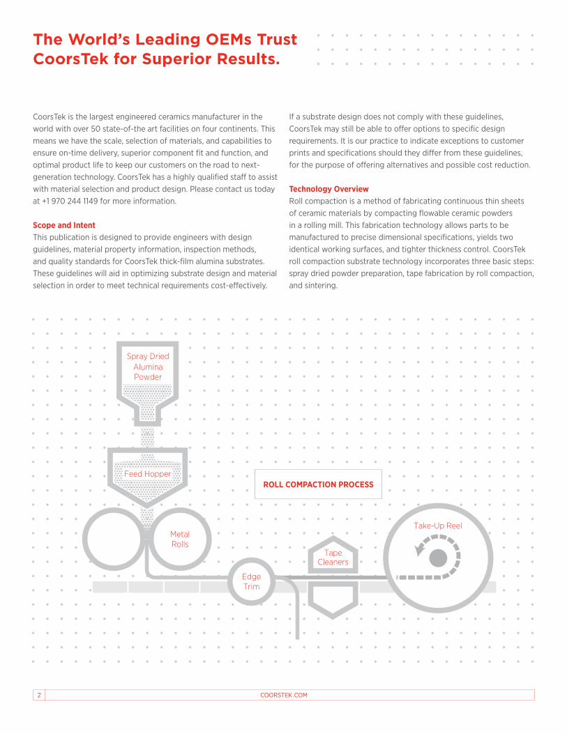
Spray DriedAluminaPowder
Take-Up Reel
TapeCleaners
MetalRolls
Feed Hopper
EdgeTrim
The World’s Leading OEMs Trust CoorsTek for Superior Results.
CoorsTek is the largest engineered ceramics manufacturer in the world with over 50 state-of-the art facilities on four continents. This means we have the scale, selection of materials, and capabilities to ensure on-time delivery, superior component fit and function, and optimal product life to keep our customers on the road to next-generation technology. CoorsTek has a highly qualified staff to assist with material selection and product design. Please contact us today at +1 970 244 1149 for more information.
Scope and Intent This publication is designed to provide engineers with design guidelines, material property information, inspection methods, and quality standards for CoorsTek thick-film alumina substrates. These guidelines will aid in optimizing substrate design and material selection in order to meet technical requirements cost-effectively.
If a substrate design does not comply with these guidelines, CoorsTek may still be able to offer options to specific design requirements. It is our practice to indicate exceptions to customer prints and specifications should they differ from these guidelines, for the purpose of offering alternatives and possible cost reduction.
Technology OverviewRoll compaction is a method of fabricating continuous thin sheets of ceramic materials by compacting flowable ceramic powders in a rolling mill. This fabrication technology allows parts to be manufactured to precise dimensional specifications, yields two identical working surfaces, and tighter thickness control. CoorsTek roll compaction substrate technology incorporates three basic steps: spray dried powder preparation, tape fabrication by roll compaction, and sintering.
ROLL COMPACTION PROCESS
3+1 970 244 1149
As-Fired Substrates Design Guidelines
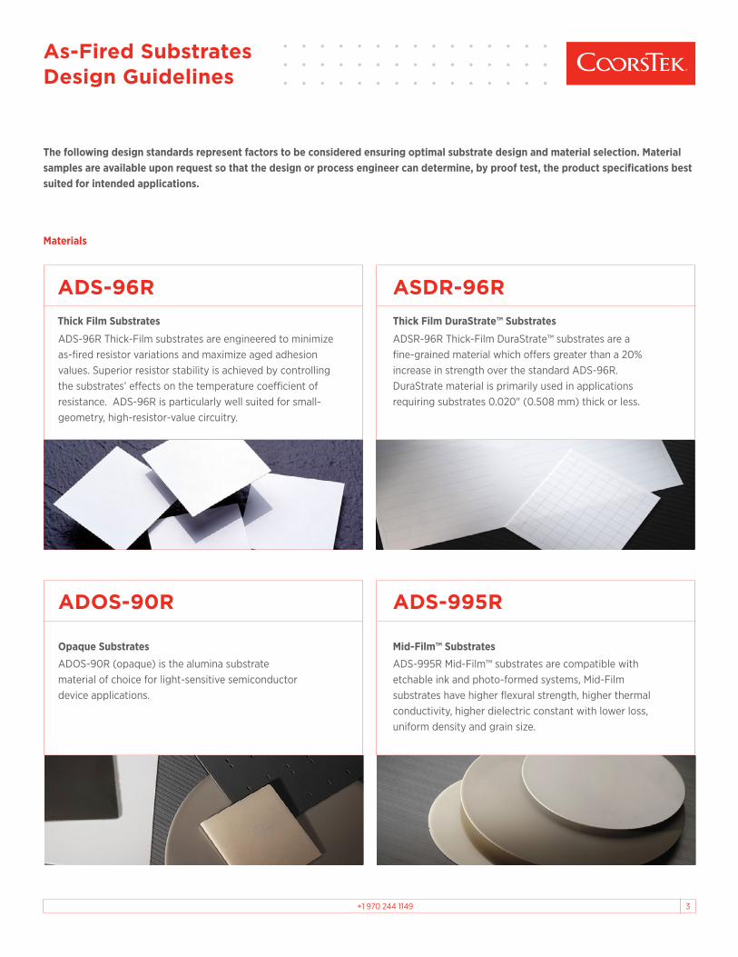
The following design standards represent factors to be considered ensuring optimal substrate design and material selection. Material samples are available upon request so that the design or process engineer can determine, by proof test, the product specifications best suited for intended applications.
ADS-995R Mid-Film™ substrates are compatible with etchable ink and photo-formed systems, Mid-Film substrates have higher flexural strength, higher thermal conductivity, higher dielectric constant with lower loss, uniform density and grain size.
Thick Film Substrates
Opaque Substrates
Thick Film DuraStrate™ Substrates
Mid-Film™ Substrates
ADS-96R
ADOS-90R
ASDR-96R
ADS-995R
ADS-96R Thick-Film substrates are engineered to minimize as-fired resistor variations and maximize aged adhesion values. Superior resistor stability is achieved by controlling the substrates’ effects on the temperature coefficient of resistance. ADS-96R is particularly well suited for small-geometry, high-resistor-value circuitry.
ADOS-90R (opaque) is the alumina substrate material of choice for light-sensitive semiconductor device applications.
Materials
ADSR-96R Thick-Film DuraStrate™ substrates are a fine-grained material which offers greater than a 20% increase in strength over the standard ADS-96R. DuraStrate material is primarily used in applications requiring substrates 0.020" (0.508 mm) thick or less.
4 COORSTEK.COM
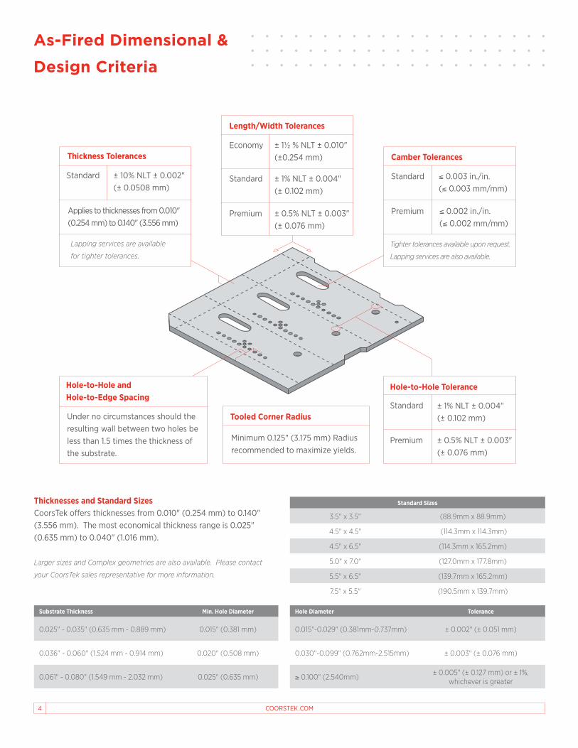
Thicknesses and Standard SizesCoorsTek offers thicknesses from 0.010" (0.254 mm) to 0.140" (3.556 mm). The most economical thickness range is 0.025" (0.635 mm) to 0.040" (1.016 mm).
Larger sizes and Complex geometries are also available. Please contact
your CoorsTek sales representative for more information.
Standard Sizes
3.5" x 3.5" (88.9mm x 88.9mm)
4.5" x 4.5" (114.3mm x 114.3mm)
4.5" x 6.5" (114.3mm x 165.2mm)
5.0" x 7.0" (127.0mm x 177.8mm)
5.5" x 6.5" (139.7mm x 165.2mm)
7.5" x 5.5" (190.5mm x 139.7mm)
± 10% NLT ± 0.002" (± 0.0508 mm)
Thickness Tolerances Camber Tolerances
≤ 0.002 in./in. (≤ 0.002 mm/mm)
Length/Width Tolerances
Economy
As-Fired Dimensional &
Design Criteria
Tooled Corner Radius
Minimum 0.125" (3.175 mm) Radius recommended to maximize yields.
± 1½ % NLT ± 0.010" (±0.254 mm)
Standard Standard Standard
± 0.5% NLT ± 0.003" (± 0.076 mm)
± 1% NLT ± 0.004" (± 0.102 mm)
Premium Premium
Tighter tolerances available upon request.
Lapping services are also available.
≤ 0.003 in./in. (≤ 0.003 mm/mm)
Applies to thicknesses from 0.010" (0.254 mm) to 0.140" (3.556 mm)
Lapping services are available
for tighter tolerances.
Hole-to-Hole Tolerance
Standard
Premium
± 1% NLT ± 0.004" (± 0.102 mm)
± 0.5% NLT ± 0.003" (± 0.076 mm)
Hole-to-Hole and Hole-to-Edge Spacing
Under no circumstances should the resulting wall between two holes be less than 1.5 times the thickness of the substrate.
Substrate Thickness Min. Hole Diameter
0.025" - 0.035" (0.635 mm - 0.889 mm) 0.015" (0.381 mm)
0.036" - 0.060" (1.524 mm - 0.914 mm) 0.020" (0.508 mm)
0.061" - 0.080" (1.549 mm - 2.032 mm) 0.025" (0.635 mm)
Hole Diameter Tolerance
0.015"-0.029" (0.381mm-0.737mm) ± 0.002" (± 0.051 mm)
0.030"-0.099" (0.762mm-2.515mm) ± 0.003" (± 0.076 mm)
≥ 0.100" (2.540mm)± 0.005" (± 0.127 mm) or ± 1%,
whichever is greater
5+1 970 244 1149
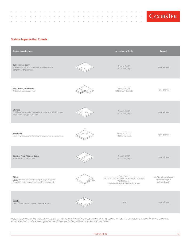
Note: The criteria in this table do not apply to substrates with surface areas greater than 35 square inches. The acceptance criteria for these large area substrates (with surface areas greater than 35 square inches) will be provided with quotation.
Surface Imperfections Acceptance Criteria Lapped
Burrs/Excess Body Fragment of excess material or foreign particle adhering to the surface
None > 0.001" (0.025 mm) High
None allowed
Pits, Holes, and Pocks A deep depression or void
None > 0.020" (0.508 mm) Diameter
None allowed
Blisters Bubble or gaseous inclusion at the surface which, if broken, could form a pit, pock, or hole
None > 0.001" (0.025 mm) High
None allowed
Scratches Relatively long, narrow, shallow groove or cut in the surface
None > 0.0007" (0.017 mm) Deep
None allowed
Bumps, Fins, Ridges, Dents Protrusions on the surface
None > 0.001" (0.025 mm) High
None allowed
Chips Open: Material broken off along an edge or corner Closed: Material has not broken off or separated
Print Face = None > 0.030" (0.762 mm) x 50% of thickness
Waste Border = unlimited length x 100% of thickness
> 0.75% substrate length unlimited length X unlimited depth
Cracks Line of fracture without complete separation
None None allowed
Surface Imperfection Criteria
6 COORSTEK.COM
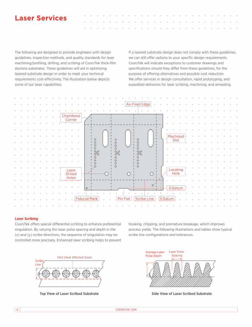
Fiducial Mark
As-Fired Edge
MachinedSlot
0 Datum
0 Datum
Scribe LinePin Flat
LaserDrilledHoles
ChamferedCorner
LocatingHole
Laser ScribingCoorsTek offers special differential scribing to enhance preferential singulation. By varying the laser pulse spacing and depth in the (x) and (y) scribe directions, the sequence of singulation may be controlled more precisely. Enhanced laser scribing helps to prevent
hooking, chipping, and premature breakage, which improves process yields. The following illustrations and tables show typical scribe line configurations and tolerances.
Top View of Laser Scribed Substrate Side View of Laser Scribed Substrate
The following are designed to provide engineers with design guidelines, inspection methods, and quality standards for laser machining/profiling, drilling, and scribing of CoorsTek thick-film alumina substrates. These guidelines will aid in optimizing lasered substrate design in order to meet your technical requirements cost-effectively. The illustration below depicts some of our laser capabilities.
If a lasered substrate design does not comply with these guidelines, we can still offer options to your specific design requirements. CoorsTek will indicate exceptions to customer drawings and specifications should they differ from these guidelines, for the purpose of offering alternatives and possible cost reduction. We offer services in design consultation, rapid prototyping, and expedited deliveries for laser scribing, machining, and annealing.
Laser Pulse Spacing
Average LaserPulse DepthHAZ (Heat A�ected Zone)
ScribeLine
Laser Services
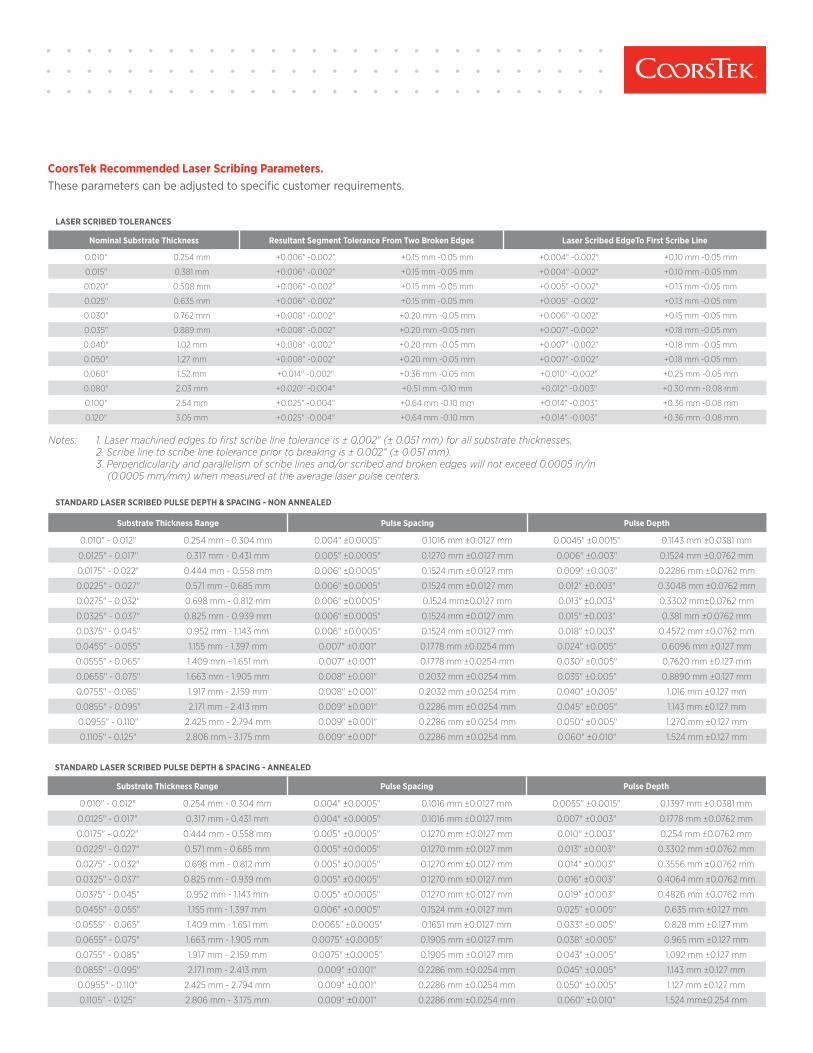
LASER SCRIBED TOLERANCES
Nominal Substrate Thickness Resultant Segment Tolerance From Two Broken Edges Laser Scribed EdgeTo First Scribe Line
0.010" 0.254 mm +0.006" -0.002" +0.15 mm -0.05 mm +0.004" -0.002" +0.10 mm -0.05 mm
0.015" 0.381 mm +0.006" -0.002" +0.15 mm -0.05 mm +0.004" -0.002" +0.10 mm -0.05 mm
0.020" 0.508 mm +0.006" -0.002" +0.15 mm -0.05 mm +0.005" -0.002" +0.13 mm -0.05 mm
0.025" 0.635 mm +0.006" -0.002" +0.15 mm -0.05 mm +0.005" -0.002" +0.13 mm -0.05 mm
0.030" 0.762 mm +0.008" -0.002" +0.20 mm -0.05 mm +0.006" -0.002" +0.15 mm -0.05 mm
0.035" 0.889 mm +0.008" -0.002" +0.20 mm -0.05 mm +0.007" -0.002" +0.18 mm -0.05 mm
0.040" 1.02 mm +0.008" -0.002" +0.20 mm -0.05 mm +0.007" -0.002" +0.18 mm -0.05 mm
0.050" 1.27 mm +0.008" -0.002" +0.20 mm -0.05 mm +0.007" -0.002" +0.18 mm -0.05 mm
0.060" 1.52 mm +0.014" -0.002" +0.36 mm -0.05 mm +0.010" -0.002" +0.25 mm -0.05 mm
0.080" 2.03 mm +0.020" -0.004" +0.51 mm -0.10 mm +0.012" -0.003" +0.30 mm -0.08 mm
0.100" 2.54 mm +0.025" -0.004" +0.64 mm -0.10 mm +0.014" -0.003" +0.36 mm -0.08 mm
0.120" 3.05 mm +0.025" -0.004" +0.64 mm -0.10 mm +0.014" -0.003" +0.36 mm -0.08 mm
CoorsTek Recommended Laser Scribing Parameters. These parameters can be adjusted to specific customer requirements.
Notes: 1. Laser machined edges to first scribe line tolerance is ± 0.002" (± 0.051 mm) for all substrate thicknesses. 2. Scribe line to scribe line tolerance prior to breaking is ± 0.002" (± 0.051 mm). 3. Perpendicularity and parallelism of scribe lines and/or scribed and broken edges will not exceed 0.0005 in/in (0.0005 mm/mm) when measured at the average laser pulse centers.
STANDARD LASER SCRIBED PULSE DEPTH & SPACING - NON ANNEALED
Substrate Thickness Range Pulse Spacing Pulse Depth
0.010" - 0.012" 0.254 mm - 0.304 mm 0.004" ±0.0005" 0.1016 mm ±0.0127 mm 0.0045" ±0.0015" 0.1143 mm ±0.0381 mm
0.0125" - 0.017" 0.317 mm - 0.431 mm 0.005" ±0.0005" 0.1270 mm ±0.0127 mm 0.006" ±0.003" 0.1524 mm ±0.0762 mm
0.0175" - 0.022" 0.444 mm - 0.558 mm 0.006" ±0.0005" 0.1524 mm ±0.0127 mm 0.009" ±0.003" 0.2286 mm ±0.0762 mm
0.0225" - 0.027" 0.571 mm - 0.685 mm 0.006" ±0.0005" 0.1524 mm ±0.0127 mm 0.012" ±0.003" 0.3048 mm ±0.0762 mm
0.0275" - 0.032" 0.698 mm - 0.812 mm 0.006" ±0.0005" 0.1524 mm±0.0127 mm 0.013" ±0.003" 0.3302 mm±0.0762 mm
0.0325" - 0.037" 0.825 mm - 0.939 mm 0.006" ±0.0005" 0.1524 mm ±0.0127 mm 0.015" ±0.003" 0.381 mm ±0.0762 mm
0.0375" - 0.045" 0.952 mm - 1.143 mm 0.006" ±0.0005" 0.1524 mm ±0.0127 mm 0.018" ±0.003" 0.4572 mm ±0.0762 mm
0.0455" - 0.055" 1.155 mm - 1.397 mm 0.007" ±0.001" 0.1778 mm ±0.0254 mm 0.024" ±0.005" 0.6096 mm ±0.127 mm
0.0555" - 0.065" 1.409 mm - 1.651 mm 0.007" ±0.001" 0.1778 mm ±0.0254 mm 0.030" ±0.005" 0.7620 mm ±0.127 mm
0.0655" - 0.075" 1.663 mm - 1.905 mm 0.008" ±0.001" 0.2032 mm ±0.0254 mm 0.035" ±0.005" 0.8890 mm ±0.127 mm
0.0755" - 0.085" 1.917 mm - 2.159 mm 0.008" ±0.001" 0.2032 mm ±0.0254 mm 0.040" ±0.005" 1.016 mm ±0.127 mm
0.0855" - 0.095" 2.171 mm - 2.413 mm 0.009" ±0.001" 0.2286 mm ±0.0254 mm 0.045" ±0.005" 1.143 mm ±0.127 mm
0.0955" - 0.110" 2.425 mm - 2.794 mm 0.009" ±0.001" 0.2286 mm ±0.0254 mm 0.050" ±0.005" 1.270 mm ±0.127 mm
0.1105" - 0.125" 2.806 mm - 3.175 mm 0.009" ±0.001" 0.2286 mm ±0.0254 mm 0.060" ±0.010" 1.524 mm ±0.127 mm
STANDARD LASER SCRIBED PULSE DEPTH & SPACING - ANNEALED
Substrate Thickness Range Pulse Spacing Pulse Depth
0.010" - 0.012" 0.254 mm - 0.304 mm 0.004" ±0.0005" 0.1016 mm ±0.0127 mm 0.0055" ±0.0015" 0.1397 mm ±0.0381 mm
0.0125" - 0.017" 0.317 mm - 0.431 mm 0.004" ±0.0005" 0.1016 mm ±0.0127 mm 0.007" ±0.003" 0.1778 mm ±0.0762 mm
0.0175" - 0.022" 0.444 mm - 0.558 mm 0.005" ±0.0005" 0.1270 mm ±0.0127 mm 0.010" ±0.003" 0.254 mm ±0.0762 mm
0.0225" - 0.027" 0.571 mm - 0.685 mm 0.005" ±0.0005" 0.1270 mm ±0.0127 mm 0.013" ±0.003" 0.3302 mm ±0.0762 mm
0.0275" - 0.032" 0.698 mm - 0.812 mm 0.005" ±0.0005" 0.1270 mm ±0.0127 mm 0.014" ±0.003" 0.3556 mm ±0.0762 mm
0.0325" - 0.037" 0.825 mm - 0.939 mm 0.005" ±0.0005" 0.1270 mm ±0.0127 mm 0.016" ±0.003" 0.4064 mm ±0.0762 mm
0.0375" - 0.045" 0.952 mm - 1.143 mm 0.005" ±0.0005" 0.1270 mm ±0.0127 mm 0.019" ±0.003" 0.4826 mm ±0.0762 mm
0.0455" - 0.055" 1.155 mm - 1.397 mm 0.006" ±0.0005" 0.1524 mm ±0.0127 mm 0.025" ±0.005" 0.635 mm ±0.127 mm
0.0555" - 0.065" 1.409 mm - 1.651 mm 0.0065" ±0.0005" 0.1651 mm ±0.0127 mm 0.033" ±0.005" 0.828 mm ±0.127 mm
0.0655" - 0.075" 1.663 mm - 1.905 mm 0.0075" ±0.0005" 0.1905 mm ±0.0127 mm 0.038" ±0.005" 0.965 mm ±0.127 mm
0.0755" - 0.085" 1.917 mm - 2.159 mm 0.0075" ±0.0005" 0.1905 mm ±0.0127 mm 0.043" ±0.005" 1.092 mm ±0.127 mm
0.0855" - 0.095" 2.171 mm - 2.413 mm 0.009" ±0.001" 0.2286 mm ±0.0254 mm 0.045" ±0.005" 1.143 mm ±0.127 mm
0.0955" - 0.110" 2.425 mm - 2.794 mm 0.009" ±0.001" 0.2286 mm ±0.0254 mm 0.050" ±0.005" 1.127 mm ±0.127 mm
0.1105" - 0.125" 2.806 mm - 3.175 mm 0.009" ±0.001" 0.2286 mm ±0.0254 mm 0.060" ±0.010" 1.524 mm±0.254 mm
8 COORSTEK.COM
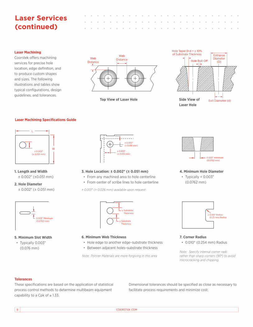
1. Length and Width ± 0.002" (±0.051 mm)
3. Hole Location: ± 0.002" (± 0.051 mm) • From any machined area to hole centerline• From center of scribe lines to hole centerline2. Hole Diameter
± 0.002" (± 0.051 mm)
4. Minimum Hole Diameter• Typically = 0.003"
(0.0762 mm)
± 0.001" (± 0.026 mm) available upon request
Note: Thinner Materials are more forgiving in this areaNote: Specify internal corner radii rather than sharp corners (90°) to avoid microcracking and chipping.
6. Minimum Web Thickness• Hole edge to another edge–substrate thickness • Between adjacent holes–substrate thickness
5. Minimum Slot Width• Typically 0.003"
(0.076 mm)
7. Corner Radius• 0.010" (0.254 mm) Radius
Laser Machining Specifications Guide
TolerancesThese specifications are based on the application of statistical process control methods to determine multibeam equipment capability to a Cpk of ≥ 1.33.
Dimensional tolerances should be specified as close as necessary to facilitate process requirements and minimize cost.
≥ 0.010" Radius (0.25 mm) Radius
± 0.002"(± 0.051 mm)
± 0.002"(± 0.051 mm)
L
± 0.002"(± 0.051 mm)
W
0.003" minimum(0.0762 mm)
0.003" Minimum(0.0762 mm) ≥ Substrate
Thickness
≥ Substrate Thickness
Laser Machining Coorstek offers machining services for precise hole location, edge definition, and to produce custom shapes and sizes. The following illustrations and tables show typical configurations, design guidelines, and tolerances.
Side View of Laser Hole
Top View of Laser Hole Exit Diameter (d)
EntranceDiameter
(D)Hole Roll-O
Hole Taper D-d = ≤ 10%of Substrate ThicknessWeb
DistanceWebDistance
Laser Services (continued)
9+1 970 244 1149
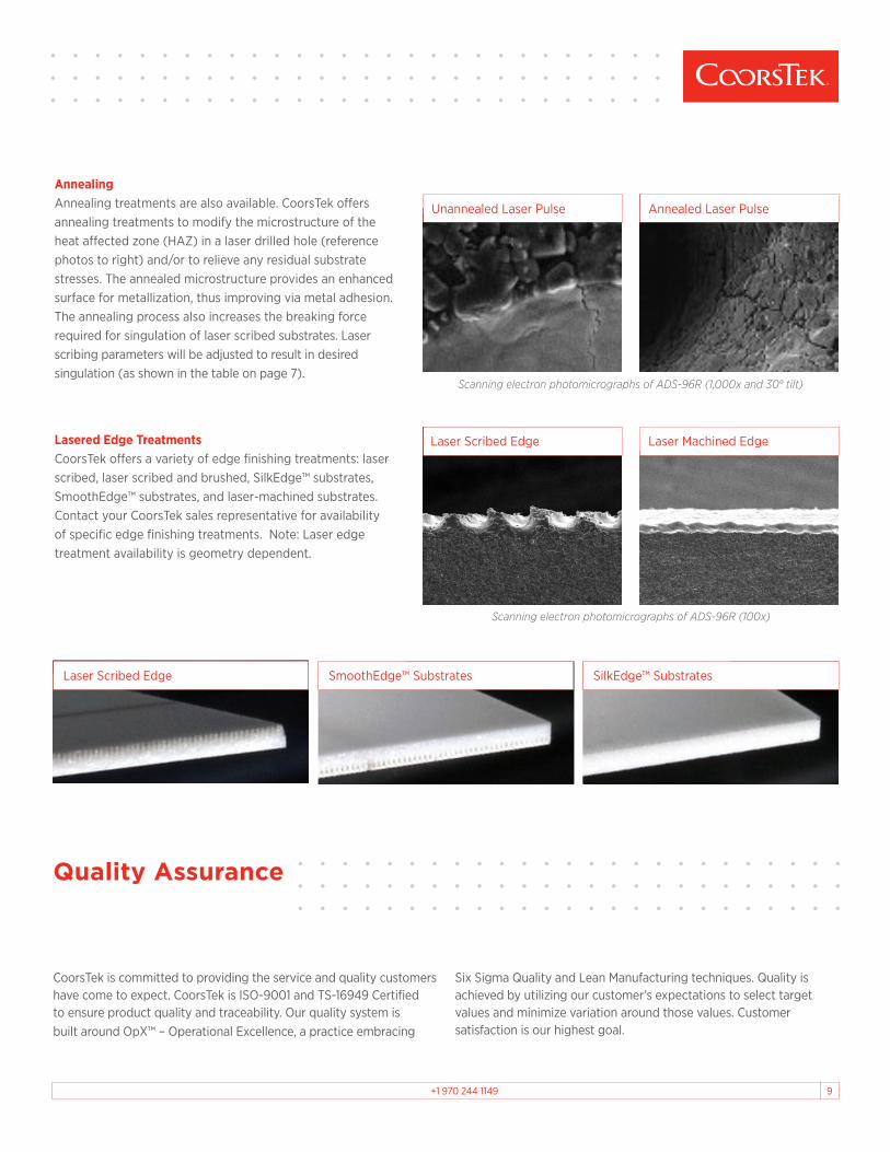
Scanning electron photomicrographs of ADS-96R (100x)
Laser Scribed Edge SilkEdge™ SubstratesSmoothEdge™ Substrates
Lasered Edge TreatmentsCoorsTek offers a variety of edge finishing treatments: laser scribed, laser scribed and brushed, SilkEdge™ substrates, SmoothEdge™ substrates, and laser-machined substrates. Contact your CoorsTek sales representative for availability of specific edge finishing treatments. Note: Laser edge treatment availability is geometry dependent.
AnnealingAnnealing treatments are also available. CoorsTek offers annealing treatments to modify the microstructure of the heat affected zone (HAZ) in a laser drilled hole (reference photos to right) and/or to relieve any residual substrate stresses. The annealed microstructure provides an enhanced surface for metallization, thus improving via metal adhesion. The annealing process also increases the breaking force required for singulation of laser scribed substrates. Laser scribing parameters will be adjusted to result in desired singulation (as shown in the table on page 7).
Unannealed Laser Pulse
Scanning electron photomicrographs of ADS-96R (1,000x and 30° tilt)
Laser Scribed Edge Laser Machined Edge
CoorsTek is committed to providing the service and quality customers have come to expect. CoorsTek is ISO-9001 and TS-16949 Certified to ensure product quality and traceability. Our quality system is built around OpX™ – Operational Excellence, a practice embracing
Six Sigma Quality and Lean Manufacturing techniques. Quality is achieved by utilizing our customer’s expectations to select target values and minimize variation around those values. Customer satisfaction is our highest goal.
Quality Assurance
Annealed Laser Pulse
10 COORSTEK.COM
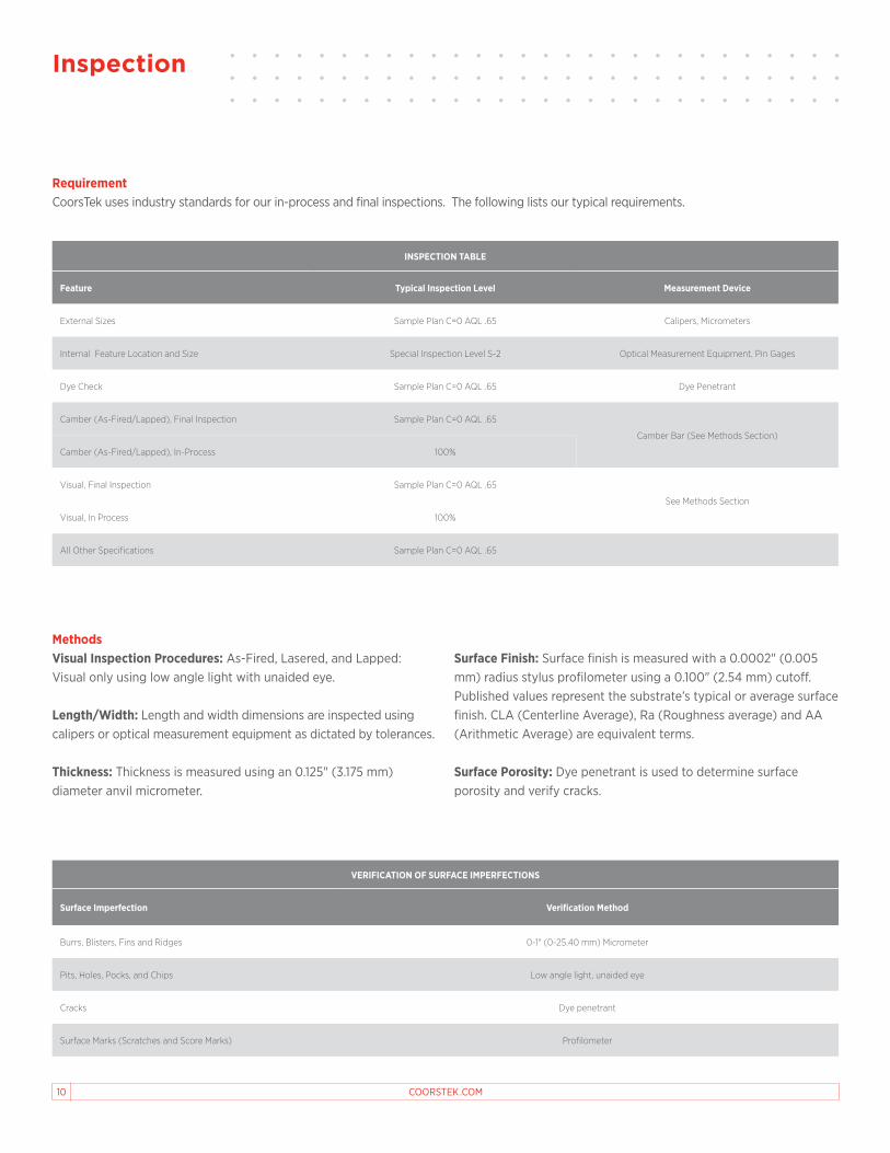
INSPECTION TABLE
Feature Typical Inspection Level Measurement Device
External Sizes Sample Plan C=0 AQL .65 Calipers, Micrometers
Internal Feature Location and Size Special Inspection Level S-2 Optical Measurement Equipment, Pin Gages
Dye Check Sample Plan C=0 AQL .65 Dye Penetrant
Camber (As-Fired/Lapped), Final Inspection Sample Plan C=0 AQL .65
Camber Bar (See Methods Section)
Camber (As-Fired/Lapped), In-Process 100%
Visual, Final Inspection Sample Plan C=0 AQL .65
See Methods Section
Visual, In Process 100%
All Other Specifications Sample Plan C=0 AQL .65
MethodsVisual Inspection Procedures: As-Fired, Lasered, and Lapped: Visual only using low angle light with unaided eye.
Length/Width: Length and width dimensions are inspected using calipers or optical measurement equipment as dictated by tolerances.
Thickness: Thickness is measured using an 0.125" (3.175 mm) diameter anvil micrometer.
Surface Finish: Surface finish is measured with a 0.0002" (0.005 mm) radius stylus profilometer using a 0.100" (2.54 mm) cutoff. Published values represent the substrate’s typical or average surface finish. CLA (Centerline Average), Ra (Roughness average) and AA (Arithmetic Average) are equivalent terms.
Surface Porosity: Dye penetrant is used to determine surface porosity and verify cracks.
Requirement CoorsTek uses industry standards for our in-process and final inspections. The following lists our typical requirements.
VERIFICATION OF SURFACE IMPERFECTIONS
Surface Imperfection Verification Method
Burrs, Blisters, Fins and Ridges 0-1" (0-25.40 mm) Micrometer
Pits, Holes, Pocks, and Chips Low angle light, unaided eye
Cracks Dye penetrant
Surface Marks (Scratches and Score Marks) Profilometer
Inspection
11+1 970 244 1149
ENGLISH EXAMPLE:
Hole Sizes and Shapes: Hole diameters and shapes are verified using computer-enhanced optical measuring with top or back light equipment or pin gauges. Method of hole verification will be chosen for best correlation on hole size between CoorsTek and customer.
Hole Locations: CoorsTek standard procedure for inspection of hole locations is computer-enhanced optical measuring equipment on the entry side using top light.
Scribe Lines: Before Break: Scribe line locations are inspected using computer-enhanced optical measuring equipment.
After Break: The part segments are inspected with digital calipers.
Chips: Inspection for chips is done under a high-intensity, low-angle light using the unaided eye.
Part Features: Location and size of part features are inspected with computer-enhanced optical measuring equipment.
Pulse Depth: Average laser pulse depth is inspected on a substrate cross section using enhanced optical methods at a magnification of 30x. The average is determined over a minimum of 10 adjacent pulses.
Pulse Spacing: Average laser pulse spacing is inspected using enhanced optical methods at a magnification of 30x. The average is determined over 11 adjacent pulses.
Slag Height: Slag height is inspected with a micrometer and is not to exceed 0.001" (0.025 mm) in height.
Cracks: Inspection for cracks is performed using a dye penetrant or other appropriate techniques.
METRIC EXAMPLE:
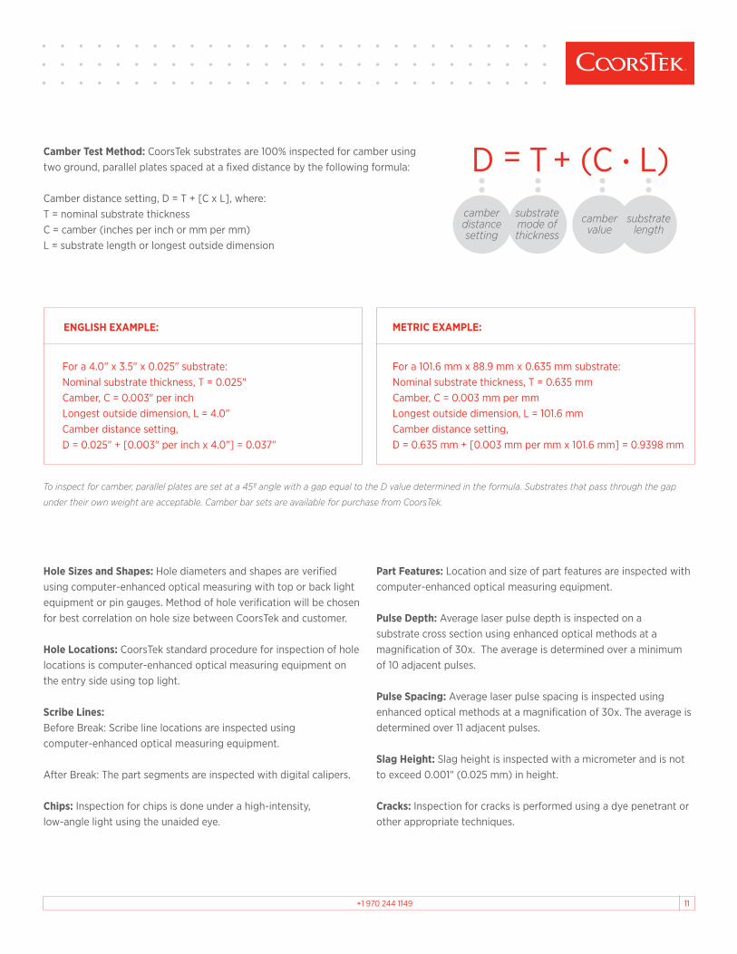
Camber Test Method: CoorsTek substrates are 100% inspected for camber using two ground, parallel plates spaced at a fixed distance by the following formula: Camber distance setting, D = T + [C x L], where: T = nominal substrate thickness C = camber (inches per inch or mm per mm) L = substrate length or longest outside dimension
To inspect for camber, parallel plates are set at a 45º angle with a gap equal to the D value determined in the formula. Substrates that pass through the gap
under their own weight are acceptable. Camber bar sets are available for purchase from CoorsTek.
D = T + (C • L)camber distance setting
substrate mode of thickness
camber value
substrate length
For a 4.0" x 3.5" x 0.025" substrate: Nominal substrate thickness, T = 0.025" Camber, C = 0.003" per inch Longest outside dimension, L = 4.0" Camber distance setting, D = 0.025" + [0.003" per inch x 4.0"] = 0.037"
For a 101.6 mm x 88.9 mm x 0.635 mm substrate: Nominal substrate thickness, T = 0.635 mm Camber, C = 0.003 mm per mm Longest outside dimension, L = 101.6 mm Camber distance setting, D = 0.635 mm + [0.003 mm per mm x 101.6 mm] = 0.9398 mm
Thick-Film Ceramic Substrates Design Guide
©2017 CoorsTekcoorstek.comAmericas
+1 303 271 7100+1 855 929 7100 toll free in [email protected]
China+86 21 6362 1125 [email protected]
Europe+44 1592 773743 [email protected]
Taiwan+886 3 5334337 [email protected] 8510-1537 rev G
(01537 G)
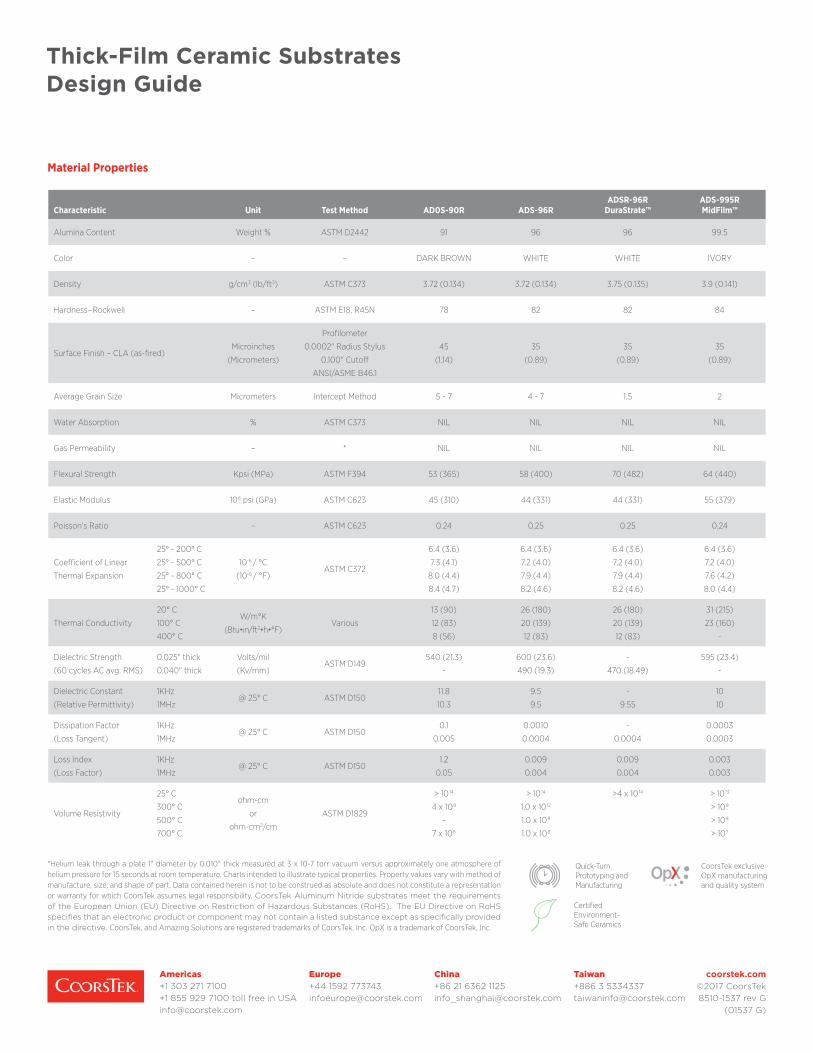
Material Properties
Certified Environment- Safe Ceramics
*Helium leak through a plate 1" diameter by 0.010" thick measured at 3 x 10⁻⁷ torr vacuum versus approximately one atmosphere of helium pressure for 15 seconds at room temperature. Charts intended to illustrate typical properties. Property values vary with method of manufacture, size, and shape of part. Data contained herein is not to be construed as absolute and does not constitute a representation or warranty for which CoorsTek assumes legal responsibility. CoorsTek Aluminum Nitride substrates meet the requirements of the European Union (EU) Directive on Restriction of Hazardous Substances (RoHS). The EU Directive on RoHS specifies that an electronic product or component may not contain a listed substance except as specifically provided in the directive. CoorsTek, and Amazing Solutions are registered trademarks of CoorsTek, Inc. OpX is a trademark of CoorsTek, Inc.
Characteristic Unit Test Method AD0S-90R ADS-96RADSR-96R
DuraStrate™ADS-995R MidFilm™
Alumina Content Weight % ASTM D2442 91 96 96 99.5
Color – – DARK BROWN WHITE WHITE IVORY
Density g/cm3 (lb/ft3) ASTM C373 3.72 (0.134) 3.72 (0.134) 3.75 (0.135) 3.9 (0.141)
Hardness–Rockwell – ASTM E18, R45N 78 82 82 84
Surface Finish – CLA (as-fired)Microinches
(Micrometers)
Profilometer
0.0002" Radius Stylus
0.100" Cutoff
ANSI/ASME B46.1
45
(1.14)
35
(0.89)
35
(0.89)
35
(0.89)
Average Grain Size Micrometers Intercept Method 5 - 7 4 - 7 1.5 2
Water Absorption % ASTM C373 NIL NIL NIL NIL
Gas Permeability – * NIL NIL NIL NIL
Flexural Strength Kpsi (MPa) ASTM F394 53 (365) 58 (400) 70 (482) 64 (440)
Elastic Modulus 106 psi (GPa) ASTM C623 45 (310) 44 (331) 44 (331) 55 (379)
Poisson's Ratio – ASTM C623 0.24 0.25 0.25 0.24
Coefficient of Linear
Thermal Expansion
25° - 200° C
25° - 500° C
25° - 800° C
25° - 1000° C
10-6 / °C
(10-6 / °F)ASTM C372
6.4 (3.6)
7.3 (4.1)
8.0 (4.4)
8.4 (4.7)
6.4 (3.6)
7.2 (4.0)
7.9 (4.4)
8.2 (4.6)
6.4 (3.6)
7.2 (4.0)
7.9 (4.4)
8.2 (4.6)
6.4 (3.6)
7.2 (4.0)
7.6 (4.2)
8.0 (4.4)
Thermal Conductivity
20° C
100° C
400° C
W/m°K
(Btu•in/ft2•h•°F)Various
13 (90)
12 (83)
8 (56)
26 (180)
20 (139)
12 (83)
26 (180)
20 (139)
12 (83)
31 (215)
23 (160)
-
Dielectric Strength
(60 cycles AC avg. RMS)
0.025" thick
0.040" thick
Volts/mil
(Kv/mm)ASTM D149
540 (21.3)
-
600 (23.6)
490 (19.3)
-
470 (18.49)
595 (23.4)
-
Dielectric Constant
(Relative Permittivity)
1KHz
1MHz@ 25° C ASTM D150
11.8
10.3
9.5
9.5
-
9.55
10
10
Dissipation Factor
(Loss Tangent)
1KHz
1MHz@ 25° C ASTM D150
0.1
0.005
0.0010
0.0004
-
0.0004
0.0003
0.0003
Loss Index
(Loss Factor)
1KHz
1MHz@ 25° C ASTM D150
1.2
0.05
0.009
0.004
0.009
0.004
0.003
0.003
Volume Resistivity
25° C
300° C
500° C
700° C
ohm-cm
or
ohm-cm2/cm
ASTM D1829
> 1014
4 x 10⁸
–
7 x 10⁶
> 1014
1.0 x 10¹²
1.0 x 10⁹
1.0 x 10⁸
>4 x 10¹⁴
> 1013
> 109
> 108
> 107
CoorsTek exclusive OpX manufacturing and quality system
Quick-TurnPrototyping and Manufacturing