Embed Size (px)
Citation preview

Design for Test of Digital Systems TDDC33
Erik LarssonDepartment of Computer Science
2
Personnel
Erik Larsson - Course leader (examinator) Email: [email protected]
Dimitar Nikolov - Course assistant Email: [email protected]
Madeleine Häger Dahlqvist - Course secretary Email: [email protected]
Aim
The purpose of the course is that students shall acquire knowledge on the importance of design of testable digital systems and develop the ability to formulate and solve problems related to testing. After completing the course, students shall be able to: describe for fundamental test and fault concepts methodical solve test related problems in a development
environment formulate and implement/apply test algorithms define and implement a minor design-for-test assignment
3
Recommended Textbook
The recommended textbook is: VLSI Test Principles and Architectures, Laung-Terng Wang,
Chen-Wen Wu, Xiaoqing Wen Hardbound, 808 pages, publication date: JUL-2006, ISBN-13: 978-0-12-370597-6 ISBN-10: 0-12-370597-5, Imprint: MORGAN KAUFFMAN
4

Alternative Literature
Principles of Testing Electronic Systems, Samiha Mourad and Yervant Zorian, ISBN: 978-0-471-31931-3, Hardcover, 440 pages, August 2000
Digital Systems Testing and Testable Design, Miron Abramovici, Melvin A. Breuer, Arthur D. Friedman ISBN: 978-0-7803-1062-9, Hardcover, 672 pages, September 1994, Wiley-IEEE Press
Essential of Electronic Testing for Memory and Mixed-Signal VLSI Circuits, Michael L. Bushnell and Vishwani D. Agrawall, 1st ed. 2000. Corr. 2nd printing, 2005, 712 p., Hardcover ISBN: 978-0-7923-7991-1
Introduction to Advanced System-on-Chip Test Design and Optimization, Erik Larsson, Series: Frontiers in Electronic Testing , Vol. 29, 2005, XVI, 388 p., Hardcover, ISBN: 978-1-4020-3207-3
5
Survey/tutorial papers
A tutorial on built-in self-test. I. Principles, Agrawal, V.D., Kime, C.R., Saluja, K.K.
A tutorial on built-in self-test. 2. Applications, Agrawal, V.D., Kime, C.R., Saluja, K.K.
Design for testability - A survey, Williams, T.W. and Parker, K.P.
Resource-constrained system-on-a-chip test: a survey, Xu, Q. and Nicolici, N.
6
Examination
TEN1: Written exam (U,3,4,5), 3 ECTS Written examination (max 40 (including 10 points from labs)
points) 5=A=34p 4=B=28p 3=C=22p
UK=Fx=less than 22p
LAB1: Laboratory work - 3 ECTS Can get up to 10 points to include in the written pre-
exam”Dugga” (note - each dugga is given at one time; no possibility repeat)
7
LaborationsRegistration The labs should be solved individually. Registration in WebReg. Questions regarding the registration are answered by Dimitar Last day for the registration is defined by DimitarGeneral instructions The labs should be handed in using the covers located by the
printers Last day of handing in the labs will be told by DimitarInstructions and guidelines Lab 1 - Test pattern generation Lab 2 - Design for test Lab 3, 4 - Boundary Scan
8

Course Outline Introduction; Manufacturing, Wafer sort, Final test, Board and
System Test, Defects, and Faults Test generation; combinational and sequential test generation Design-for-Test techniques; test point insertion, scan, enhanced
scan Built-In Self-Test; Logic BIST and memory BIST System Chip Test; test architectures, test planning, test
scheduling, and test data compression, power constraints, test data compression.
System Test and boundary Scan Two invited speakers from SAAB Study visit to Flextronics
Late Course Registration
Please find the correct form from:http://www.lith.liu.se/blanketter/
Fill the form and give it to Patrick Lambrix (director of studies) in office: B 2B:474, Building B, Ground Floor
10
Design for Test of Digital Systems TDDC33
Erik LarssonDepartment of Computer Science
Outline
Electronics Manufacturing Test, diagnosis, and verification Cost, defects, fault models, and quality of test
12

Products with electronic systems
13
16
Production of electronic products
Wafer
IC
Board
“System”
14
Making electronic products
15
Production ProductDesign specificationDesign
Types of products: - First of a kind: product that breaks new ground- Me too with a twist: improve existing product (example, fast bus)- Derivate: add a little more functionality- Next-generation product: replace mature product
Transistor Count
16

Integrated Circuits (ICs)
Small Scale Integration (SSI), early 1960sexample, Philips TAA320 had two transistors
Medium Scale Integration (MSI), late 1960sexample, Intel 4004 had 2300 transistors
Large Scale Integration (LSI), mid-1970sexample, Intel 8008 had 4500 transistors
Very-Large Scale Integration (VLSI), 1980s,example, Intel 80286, 134000 transistors
Ultra-Large Scale Integration (ULSI), now,more than 1 million transistors Wafer-scale integration (WSI)
System-on-a-chip Three dimensional integrated circuits (3D-ICs)
17
17
IC
Viper 2.0 RevB Analog/Digital TV Processor 10mm x 10 mm (100 mm2) ~10 M gates ~50 M transistors ~100 clock domains
18
Die
19
Printed Circuit Board (PCB)
19
35
Multi-board system
20
Backplane

Types of systems
Analog systems Digital systems Mixed signal systems
21
Digital systems
22
Manufacturing
23
21
AND-gate
24
17
IC
Viper 2.0 RevB Analog/Digital TV Processor 10mm x 10 mm (100 mm2) ~10 M gates ~50 M transistors ~100 clock domains
25
Die
26
IC manufacturing
Si-substrate
Si-substrate Si-substrate
(a) Silicon base material
(b) After oxidation and depositionof negative photoresist
(c) Stepper exposure
PhotoresistSiO2
UV-lightPatternedoptical mask
Exposed resist
SiO2
Si-substrate
Si-substrate
Si-substrate
SiO2
SiO2
(d) After development and etching of resist,chemical or plasma etch of SiO2
(e) After etching
(f) Final result after removal of resist
Hardened resist
Hardened resist
Chemical or plasmaetch
36
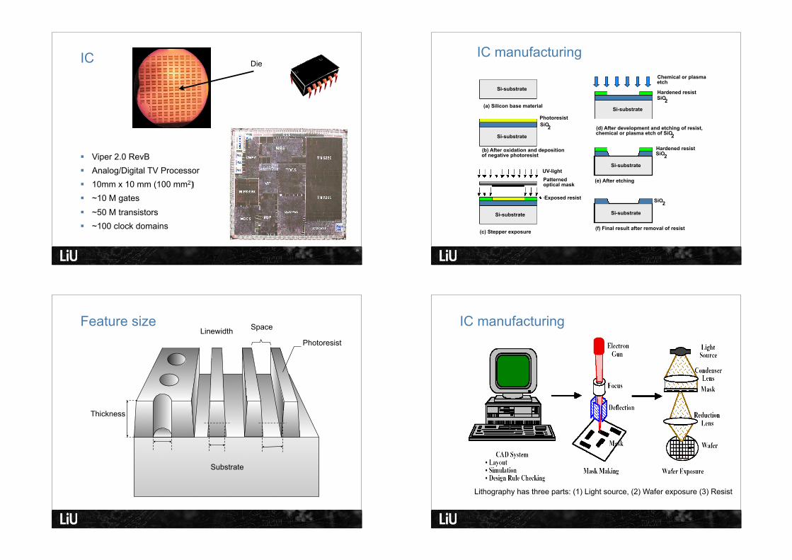
Feature sizeLinewidth Space
Thickness
Substrate
Photoresist
35
IC manufacturing
Lithography has three parts: (1) Light source, (2) Wafer exposure (3) Resist

39
Bonding Techniques
Flip-chip
42
Package-to-Board Interconnect
Outline
Electronics Manufacturing Defects, test, diagnosis, and verification Cost, defects, fault models, and quality of test
31
44
IC Defects
Salt
Seed
70
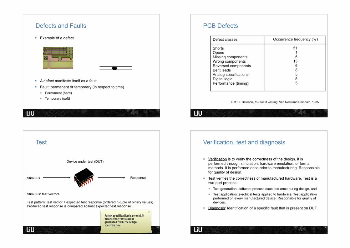
Defects and Faults
Example of a defect
A defect manifests itself as a fault Fault: permanent or temporary (in respect to time)
Permanent (hard) Temporary (soft)
69
PCB Defects
Ref.: J. Bateson, In-Circuit Testing, Van Nostrand Reinhold, 1985.
Defect classes
ShortsOpensMissing componentsWrong componentsReversed componentsBent leadsAnalog specificationsDigital logicPerformance (timing)
Occurrence frequency (%)
51 1 613 6 8 5 5 5
Test
35
Device under test (DUT)
Stimulus
Stimulus: test vectors
Test pattern: test vector + expected test response (ordered n-tuple of binary values)Produced test response is compared against expected test response
Response
Design specification is correct. It means that tests can be generated from the design specification.
47
Verification, test and diagnosis
Verification is to verify the correctness of the design. It is performed through simulation, hardware emulation, or formal methods. It is performed once prior to manufacturing. Responsible for quality of design.
Test verifies the correctness of manufactured hardware. Test is a two-part process: Test generation: software process executed once during design, and Test application: electrical tests applied to hardware. Test application
performed on every manufactured device. Responsible for quality of devices.
Diagnosis: Identification of a specific fault that is present on DUT.
36

67
Diagnosis and volume production
Yield
First silicon Ramp-up Volume production
Diagnosis
Pass/fail testing
Outline
Electronics Manufacturing Defects, test, diagnosis, and verification Cost, defects, fault models, and quality of test
38
45
Making fault free electronic products
ok?
Test Preparation Production Test In-Field Test
ok?ok?
ok?
ok?
Rule of ten: Finding a defect in one later step increases cost with a factor 10 compared to addressing the defect in current step.
Types of Test Production
Wafer sort (or probe) Test of die on the wafer
Final test (package) Test of packaged chips
Acceptance Test to demonstrate compliance with purchaser’s requirements
Sample Test some but not all parts Go/No-go Pass or fail test Characterization Test actual parameters
(performance) Stress screening (burn-in) At high temperature to get wear-
out Diagnostic (repair) Test to pinpoint defective part On-line Test while system is in operation
40

Types of Test
Wafer sort - tests the logic of each die on the wafer
Final test - tests the logic of each packaged IC
Board test - tests interconnections (soldering errors)
41
Important aspects Specify the test vector Determine correct response (expected response) Evaluate quality of test
Fault coverage = No of faults detected / No. faults modeled Defect level (DL) = Number of faulty units shipped / Total number of
units shipped. Yield = Number of good parts / Total number of tested parts Williams and Brown (1981): DL=1-Y(1-T)
where Y is yield and T is ratio of covered parts by test. For example:
If possible to test for all defects: T=1 -> DL=1-Y(1-1) =0
If no defective units manufactured: Y=1 -> DL=1-1 (1-T)=0 (T can be 0)42
58
Manufacturing Test
Determines whether manufactured chip meets specs Must cover high % of modeled faults Must minimize test time (to control cost) No fault diagnosis Tests every device on chip Test at speed of application or speed guaranteed by supplier
43
May 8, 2008 52
Testing
Device under test00101000110000
Test stimuli (TS)
Compare
Automatic Test Equipment (ATE)
Pass/fail
Expected responses (ER)10110011101010
01110110100101
Produced responses (PR)

Tests
Good IC that pass test -> OKBad IC that fail test -> OK
Bad ICs that pass test -> test escapeGood ICs that fail test -> yield loss
45
Outcome of test
Outcome of test
Pass Fail
IC
Good OK Yield loss
ICBad Test
esc. OK
Automatic Test Equipment Components
Consists of: Powerful computer
Powerful 32-bit Digital Signal Processor (DSP) for analog testing Test Program (written in high-level language) running on the
computer
Probe Head (actually touches the bare or packaged chip to perform fault detection experiments)
Probe Card or Membrane Probe(contains electronics to measure signals on chip pin or pad)
46
63
Automatic Test Equipment Companies
Teradyne was founded in 1960 by two classmates from Massachusetts Institute of Technology (MIT). http://www.teradyne.com/
LTX was founded in 1976 and the headquarter is in Norwood, MA (Greater Boston), http://www.ltx.com/
Credence Systems, Founded in 1978 as Semiconductor Test Solutions, http://www.credence.com/
LTXCredence merger 2008, http://www.ltxc.com
May 8, 2008 64
Automatic Test Equipment Companies
Agilent Technologies (formed in 1999 from a division of Hewlett-Packard), www.agilent.com
Eagle Test Systems was founded in 1976. The headquarters is in Buffalo Grove, Illinois, (merged to Teradyne 2008), http://www.eagletest.com/
Advantest Corporation (Kabushiki-gaisha Adobantesuto), founded in 1954. Headquarter in Tokyo, Japan.
Verigy was in 2006 formed from a division of Agilent Technologies, now part os Advantest, https://www.verigy.com/

May 8, 2008 65
Sapphire from Credence V93000 from Verigy T6577 from Advantest Tiger from Teradyne
Automatic Test Equipments (ATEs)
72
Test generation
ab
z
a b z0 0 00 1 01 0 01 1 1
71
Fault models
Stuck-at Fault, Bridging Fault, Shorts (Resistive shorts), Opens, Delay Faults, Transient Fault
So far stuck-at fault model is the most used one: Motivations:
Simple Covers quite well possible defects
Above 65 nm: SA0 and SA1 At 65 nm -> TSMC standard: 6 fault types; DC-SA0/SA1, AC-
input slow to rise (ISR), input slow to fall (ISF), output slow to rise (OSR), output slow to fall (OSF)
Below 65 nm (i.e 45 nm and 32 nm): ??
May 8, 2008 73
Test generation
FaultyVdd
Fault-free
X0
X0
0 1
Example: Create test for output connected to Vdd
11 1 11
1

May 8, 2008 73
Test generation
FaultyVdd
Fault-free
X0
X0
0 1
Example: Create test for output connected to Vdd
Find test stimuli such that test responses are different in fault-free and faulty device
74
Stuck-at Fault
A line is fixed to logic value 0 (stuck-at-0) or 1 (stuck-at-1) For the stuck-at fault model there are for a circuit with n lines
2*n possible fault sites
Quality of a test is given by: fault coverage = faults detected / total number of faults
Example: 10 lines (20 faults) detect 12 faults: f.c.=12/20 (60%)
ORNOR
AZ
BAND
NOR
AND
UW
X
Y
F
H
GG1
G2
G3
G4
G5
76
Single Stuck-at Fault
Three properties define a single stuck-at fault Only one line is faulty The faulty line is permanently set to 0 or 1 The fault can be at an input or output of a gate
Example: XOR circuit has 12 fault sites ( ) and 24 single stuck-at faults
a
b
c
d
e
f
10
g h i 1
s-a-0j
k
z
1(0)0(1)
1
Test vector for h s-a-0 fault
Good circuit valueFaulty circuit value
Design for Test of Digital Systems TDDC33
Erik LarssonDepartment of Computer Science