Embed Size (px)
Citation preview

Power Integrations
5245 Hellyer Avenue, San Jose, CA 95138 USA. Tel: +1 408 414 9200 Fax: +1 408 414 9201
www.powerint.com
Design Example Report
Title 7.3 W Dual Output Non-Isolated Power Supply using TNY266P
Specification Input: 90 – 265 VAC Output: 5V / 500mA, 24V / 200mA
Application Cook Top Control
Author Power Integrations Applications Department
Document Number DER-110
Date October 26, 2005
Revision 1.0
Summary and Features
• Compact 1.5” X 2” X 1” PCB footprint • Total output power 6.0 W with TNY266P and EE16 core • Typical Efficiency 75 % • Good cross regulation using low-cost zener • Meets EN55022 class B conducted EMI test without Y1 safety capacitor • No Optocoupler used in the feedback loop
The products and applications illustrated herein (including circuits external to the products and transformer construction) may be covered by one or more U.S. and foreign patents or potentially by pending U.S. and foreign patent applications assigned to Power Integrations. A complete list of Power Integrations’ patents may be found at www.powerint.com.

DER-110 Dual Output Non-Isolated Power Supply October 26, 2005
Page 2 of 23
Power IntegrationsTel: +1 408 414 9200 Fax: +1 408 414 9201
www.powerint.com
Table Of Contents 1 Introduction.................................................................................................................3 2 Power Supply Specification ........................................................................................4 3 Schematic...................................................................................................................5 4 PCB Layout ................................................................................................................6 5 Bill Of Materials...........................................................................................................7 6 Transformer Specification...........................................................................................8
6.1 Electrical Diagram ...............................................................................................8 6.2 Electrical Specifications.......................................................................................8 6.3 Materials..............................................................................................................8 6.4 Transformer Build Diagram .................................................................................9 6.5 Transformer Construction....................................................................................9
7 Transformer Spreadsheets .......................................................................................10 8 Performance Data.....................................................................................................13
8.1 Efficiency ...........................................................................................................13 8.2 No-load Input Power..........................................................................................14 8.3 Regulation .........................................................................................................15
8.3.1 Load ...........................................................................................................15 8.3.2 Line ............................................................................................................16
9 Waveforms ...............................................................................................................17 9.1 Drain Voltage and Current, Normal Operation...................................................17 9.2 Output Voltage Start-up Profile..........................................................................17 9.3 Drain Voltage and Current Start-up Profile ........................................................18 9.4 Load Transient Response (50% to 100% Load Step)........................................18 9.5 Output Ripple Measurements............................................................................19
9.5.1 Ripple Measurement Technique.................................................................19 9.5.2 Measurement Results ................................................................................20
10 Conducted EMI .....................................................................................................21 11 Revision History ....................................................................................................22 Important Notes: Although this board is designed to satisfy safety isolation requirements, the engineering prototype has not been agency approved. Therefore, all testing should be performed using an isolated source to provide power to the prototype board. Design Reports contain a power supply design specification, schematic, bill of materials, and transformer documentation. Performance data and typical operation characteristics are included. Typically only a single prototype has been built.

DER-110 Dual Output Non-Isolated Power Supply October 26, 2005
Page 3 of 23
Power IntegrationsTel: +1 408 414 9200 Fax: +1 408 414 9201
www.powerint.com
1 Introduction This document is an engineering report describing a dual output non-isolated power supply utilizing a TNY266P. This power supply is intended as a power supply for a cooktop control module. The document contains the power supply specification, schematic, bill-of-materials, transformer documentation, printed circuit layout, and performance data.
Figure 1 – Populated Circuit Board Photograph

DER-110 Dual Output Non-Isolated Power Supply October 26, 2005
Page 4 of 23
Power IntegrationsTel: +1 408 414 9200 Fax: +1 408 414 9201
www.powerint.com
2 Power Supply Specification
Description Symbol Min Typ Max Units Comment
Input Voltage VIN 90 265 VAC 2 Wire – no P.E.
Frequency fLINE 47 50/60 64 Hz
No-load Input Power (230 VAC) 0.7 W
Output
Output Voltage 1 VOUT1 5 V ± 5%
Output Ripple Voltage 1 VRIPPLE1 50 mV 20 MHz bandwidth
Output Current 1 IOUT1 500 mA
Output Voltage 2 VOUT1 24 V ± 15%
Output Ripple Voltage 2 VRIPPLE1 200 mV 20 MHz bandwidth
Output Current 2 IOUT1 200 mA
Output Power POUT 7.3 W
Efficiency η 80 % Measured at POUT (7.3 W), 25 oC
Environmental
Conducted EMI Meets CISPR22B / EN55022B
Safety Designed to meet IEC950, UL1950 Class II
Surge 4 kV
1.2/50 µs surge, IEC 1000-4-5, Series Impedance:
Differential Mode: 2 Ω Common Mode: 12 Ω
Surge 3 kV 100 kHz ring wave, 500 A short circuit current, differential and
common mode
Ambient Temperature TAMB 0 70 oC Free convection, sea level

DER-110 Dual Output Non-Isolated Power Supply October 26, 2005
Page 5 of 23
Power IntegrationsTel: +1 408 414 9200 Fax: +1 408 414 9201
www.powerint.com
3 Schematic
Figure 2 – Schematic

DER-110 Dual Output Non-Isolated Power Supply October 26, 2005
Page 6 of 23
Power IntegrationsTel: +1 408 414 9200 Fax: +1 408 414 9201
www.powerint.com
4 PCB Layout
Figure 3 – Printed Circuit Layout

DER-110 Dual Output Non-Isolated Power Supply October 26, 2005
Page 7 of 23
Power IntegrationsTel: +1 408 414 9200 Fax: +1 408 414 9201
www.powerint.com
5 Bill Of Materials Item QTY Ref. Des. Description Mfg Mfg Part Number
1 2 C1 C2 22 uF, 400 V, Electrolytic, Low ESR, 901 mOhm, (16 x 20) United Chemi-Con KMX400VB22RM16X20LL
2 1 C3 330 uF, 35 V, Electrolytic, Very Low ESR, 38 mOhm, (10 x 16) United Chemi-Con KZE35VB331MJ16LL
3 1 C4 1000 uF, 10 V, Electrolytic, Low ESR, 80 mOhm, (8 x 20) United Chemi-Con LXZ10VB102MH20LL
4 2 C5 C7 100 nF, 50 V, Ceramic, X7R, 0805 Panasonic ECU-V1H221KBN
5 1 C6 2.2 nF, 1 kV, Disc Ceramic NIC Components Corp NCD222K1KVY5F
6 1 C8 100 uF, 10 V, Electrolytic, Low ESR, 500 mOhm, (5 x 11.5) United Chemi-Con LXZ10VB101ME11LL
7 1 D1 1000 V, 1 A, Rectifier, Glass Passivated, DO-213AA (MELF) Diodes Inc DL4007
8 1 D2 400 V, 1 A, Rectifier, Glass Passivated Diodes Inc S1GB-13
9 1 D3 40 V, 1 A, Schottky, DO-214AC Vishay SS14
10 1 D4 200 V, 1 A, Ultrafast Recovery, 25 ns, DO-214AC Vishay ES1C
11 1 L1 1000 uH, 0.29 A Tokin SBC4-102-291
12 1 L2 3.3 uH, 2.66 A Toko 822LY-3R3M
13 1 Q1 NPN, Small Signal BJT, 40 V, 0.2 A, SOT-23 Vishay MMBT3904
14 1 R1 75 R, 5%, 1/8 W, Metal Film, 0805 Panasonic ERJ-6GEYJ750V
15 1 R2 200 k, 5%, 1 W, Metal Oxide Yageo RSF100JB-200K
16 1 R3 100 R, 5%, 1/8 W, Metal Film, 0805 Panasonic ERJ-6GEYJ101V
17 1 R4 330 R, 5%, 1/8 W, Metal Film, 0805 Panasonic ERJ-6GEYJ331V
18 1 R5 10 R, 5%, 1/8 W, Metal Film, 0805 Panasonic ERJ-6GEYJ100V
19 1 RF1 8.2 R, 2.5 W, Fusible/Flame Proof Wire Wound Vitrohm CRF253-4 5T 8R2
20 1 T1 Bobbin, EE16, Vertical, 8 pins Bu Chang Ind Co Ltd
21 1 U1 TinySwitch-II, TNY266P, DIP-8B Power Integrations TNY266P
22 1 VR1 4.3 V, 5%, 500 mW, DO-213AA (MELF) Diodes Inc ZMM5229B-7

DER-110 Dual Output Non-Isolated Power Supply October 26, 2005
Page 8 of 23
Power IntegrationsTel: +1 408 414 9200 Fax: +1 408 414 9201
www.powerint.com
6 Transformer Specification
6.1 Electrical Diagram
Figure 4 – Transformer Electrical Diagram
6.2 Electrical Specifications
Electrical Strength 1 second, 60 Hz, from Pins 1-4 to Pins 5-10 200 VAC
Primary Inductance Pins 1-4, all other windings open, measured at 100 kHz, 0.4 VRMS
1570 µH, -0/+20%
Resonant Frequency Pins 1-4, all other windings open 800 kHz (Min.)
Primary Leakage Inductance Pins 1-4, with Pins 5-10 shorted, measured at 100 kHz, 0.4 VRMS 60 µH (Max.)
6.3 Materials
Item Description [1] Core: EE16 PC40 Al = 124nH/T2 [2] Bobbin: 10-pin Vertical [3] Magnet Wire: #34 Heavy Build [4] Magnet Wire: #33 Heavy Build [5] Magnet Wire: #27 Heavy Build [6] Tape, 3M [7] Varnish

DER-110 Dual Output Non-Isolated Power Supply October 26, 2005
Page 9 of 23
Power IntegrationsTel: +1 408 414 9200 Fax: +1 408 414 9201
www.powerint.com
6.4 Transformer Build Diagram
Figure 5 – Transformer Build Diagram
6.5 Transformer Construction
Core Shield Start at pin 6 and wind 20 turns of bifilar wound #34. Do not connect finish end of this winding.
Basic Insulation Apply three layers of tape for basic insulation.
Primary Start on pin 4, wind 108 turns of #33 in three layers. Apply one layer of tape between each adjacent winding layer.
Basic Insulation Apply two layers of tape for basic insulation. Secondary Winding Start on pin 5, wind 6 turns of trifilar #27 in one layer. Finish on pin 6. Secondary Winding Start on pin 8, wind 21 turns of #27 in one layer. Finish on pin 5.
Outer Wrap Wrap windings with 3 layers of tape.
Final Assembly Assemble and secure core halves. Dip varnish, do not impregnate (item [7]).
DER-110 Dual Output Non-Isolated Power Supply October 26, 2005
Page 10 of 23
Power IntegrationsTel: +1 408 414 9200 Fax: +1 408 414 9201
www.powerint.com
7 Transformer Spreadsheets ACDC_TNY-
II_020105; Rev.2.4;
Copyright Power
Integrations Inc. 2005 INPUT INFO OUTPUT UNIT
ACDC_TNYII_020105_Rev2-4.xls; TinySwitch-II Continuous/Discontinuous Flyback Transformer Design Spreadsheet
ENTER APPLICATION VARIABLES Customer VACMIN 85 Volts Minimum AC Input Voltage VACMAX 265 Volts Maximum AC Input Voltage fL 50 Hertz AC Mains Frequency VO 5 Volts Output Voltage PO 7.3 Watts Output Power n 0.7 Efficiency Estimate Z 0.5 Loss Allocation Factor
tC 3 mSeconds Bridge Rectifier Conduction Time Estimate
CIN 20 uFarads Input Filter Capacitor
ENTER TinySwitch-II VARIABLES
TinySwitch-II tny266
Universal 115 Doubled/230V
Chosen Device TNY266 Power Out 9.5W 15W
ILIMITMIN 0.325 Amps TinySwitch-II Minimum Current Limit ILIMITMAX 0.375 Amps TinySwitch-II Maximum Current Limit fS 132000 Hertz TinySwitch-II Switching Frequency fSmin 120000 Hertz TinySwitch-II Minimum Switching Frequency (inc. jitter) fSmax 144000 Hertz TinySwitch-II Maximum Switching Frequency (inc. jitter) VOR 99 Volts Reflected Output Voltage VDS 10 Volts TinySwitch-II on-state Drain to Source Voltage VD 0.5 Volts Output Winding Diode Forward Voltage Drop
KP 0.67 Ripple to Peak Current Ratio (0.6<KRP<1.0 : 1.0<KDP<6.0)
ENTER TRANSFORMER CORE/CONSTRUCTION VARIABLES Core Type EE16 Core EE16 P/N: PC40EE16-Z
Bobbin EE16_B
OBBIN P/N: BE-16-118CPH AE 0.192 cm^2 Core Effective Cross Sectional Area LE 3.5 cm Core Effective Path Length AL 1140 nH/T^ Ungapped Core Effective Inductance

DER-110 Dual Output Non-Isolated Power Supply October 26, 2005
Page 11 of 23
Power IntegrationsTel: +1 408 414 9200 Fax: +1 408 414 9201
www.powerint.com
2 BW 8.5 mm Bobbin Physical Winding Width
M 0 mm Safety Margin Width (Half the Primary to Secondary Creepage Distance)
L 3 Number of Primary Layers NS 6 Number of Secondary Turns DC INPUT VOLTAGE PARAMETERS VMIN 85 Volts Minimum DC Input Voltage VMAX 375 Volts Maximum DC Input Voltage CURRENT WAVEFORM SHAPE PARAMETERS DMAX 0.57 Maximum Duty Cycle IAVG 0.12 Amps Average Primary Current IP 0.33 Amps Minimum Peak Primary Current IR 0.22 Amps Primary Ripple Current IRMS 0.17 Amps Primary RMS Current TRANSFORMER PRIMARY DESIGN PARAMETERS LP 1570 uH Primary Inductance NP 108 Primary Winding Number of Turns
ALG 135 nH/T^2 Gapped Core Effective Inductance
BM 2840 Gauss Maximum Flux Density, (BP<3100)
BAC 824 Gauss AC Flux Density for Core Loss Curves (0.5 X Peak to Peak)
ur 1654 Relative Permeability of Ungapped Core LG 0.16 mm Gap Length (Lg > 0.1 mm) BWE 25.5 mm Effective Bobbin Width OD 0.24 mm Maximum Primary Wire Diameter including insulation INS 0.05 mm Estimated Total Insulation Thickness (= 2 * film thickness) DIA 0.19 mm Bare conductor diameter
AWG 33 AWG Primary Wire Gauge (Rounded to next smaller standard AWG value)
CM 51 Cmils Bare conductor effective area in circular mils
CMA 299 Cmils/Amp Primary Winding Current Capacity (200 < CMA < 500)
TRANSFORMER SECONDARY DESIGN PARAMETERS Lumped parameters ISP 5.85 Amps Peak Secondary Current ISRMS 2.66 Amps Secondary RMS Current IO 1.46 Amps Power Supply Output Current IRIPPLE 2.22 Amps Output Capacitor RMS Ripple Current CMS 531 Cmils Secondary Bare Conductor minimum circular mils AWGS 22 AWG Secondary Wire Gauge (Rounded up to next larger
DER-110 Dual Output Non-Isolated Power Supply October 26, 2005
Page 12 of 23
Power IntegrationsTel: +1 408 414 9200 Fax: +1 408 414 9201
www.powerint.com
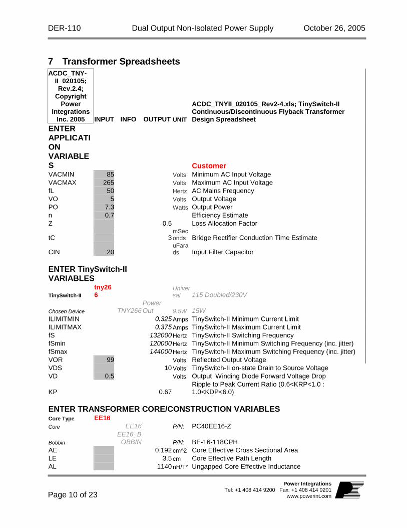
standard AWG value) DIAS 0.65 mm Secondary Minimum Bare Conductor Diameter
ODS 1.42 mm Secondary Maximum Outside Diameter for Triple Insulated Wire
INSS 0.39 mm Maximum Secondary Insulation Wall Thickness VOLTAGE STRESS PARAMETERS
VDRAIN 603 Volts Maximum Drain Voltage Estimate (Includes Effect of Leakage Inductance)
PIVS 26 Volts Output Rectifier Maximum Peak Inverse Voltage TRANSFORMER SECONDARY DESIGN PARAMETERS (MULTIPLE OUTPUTS)
1st output
VO1 5 5 Volts Output Voltage (if unused, defaults to single output design)
IO1 0.5 0.500 Amps Output DC Current PO1 2.50 Watts Output Power VD1 0.5 0.5 Volts Output Diode Forward Voltage Drop NS1 6.00 Output Winding Number of Turns ISRMS1 0.910 Amps Output Winding RMS Current IRIPPLE1 0.76 Amps Output Capacitor RMS Ripple Current PIVS1 26 Volts Output Rectifier Maximum Peak Inverse Voltage CMS1 182 Cmils Output Winding Bare Conductor minimum circular mils
AWGS1 27 AWG Wire Gauge (Rounded up to next larger standard AWG value)
DIAS1 0.36 mm Minimum Bare Conductor Diameter ODS1 1.42 mm Maximum Outside Diameter for Triple Insulated Wire 2nd output VO2 24 Volts Output Voltage IO2 0.2 Amps Output DC Current PO2 4.80 Watts Output Power VD2 0.6 Volts Output Diode Forward Voltage Drop NS2 26.84 Output Winding Number of Turns ISRMS2 0.364 Amps Output Winding RMS Current IRIPPLE2 0.30 Amps Output Capacitor RMS Ripple Current PIVS2 117 Volts Output Rectifier Maximum Peak Inverse Voltage CMS2 73 Cmils Output Winding Bare Conductor minimum circular mils
AWGS2 31 AWG Wire Gauge (Rounded up to next larger standard AWG value)
DIAS2 0.23 mm Minimum Bare Conductor Diameter ODS2 0.32 mm Maximum Outside Diameter for Triple Insulated Wire

DER-110 Dual Output Non-Isolated Power Supply October 26, 2005
Page 13 of 23
Power IntegrationsTel: +1 408 414 9200 Fax: +1 408 414 9201
www.powerint.com
8 Performance Data All measurements performed at room temperature, 60 Hz input frequency.
8.1 Efficiency
Figure 6 – Efficiency at Full Load vs. Input Voltage, Room Temperature, 60 Hz.

DER-110 Dual Output Non-Isolated Power Supply October 26, 2005
Page 14 of 23
Power IntegrationsTel: +1 408 414 9200 Fax: +1 408 414 9201
www.powerint.com
8.2 No-load Input Power
Figure 7 – Zero Load Input Power vs. Input Line Voltage, Room Temperature, 60 Hz.
DER-110 Dual Output Non-Isolated Power Supply October 26, 2005
Page 15 of 23
Power IntegrationsTel: +1 408 414 9200 Fax: +1 408 414 9201
www.powerint.com
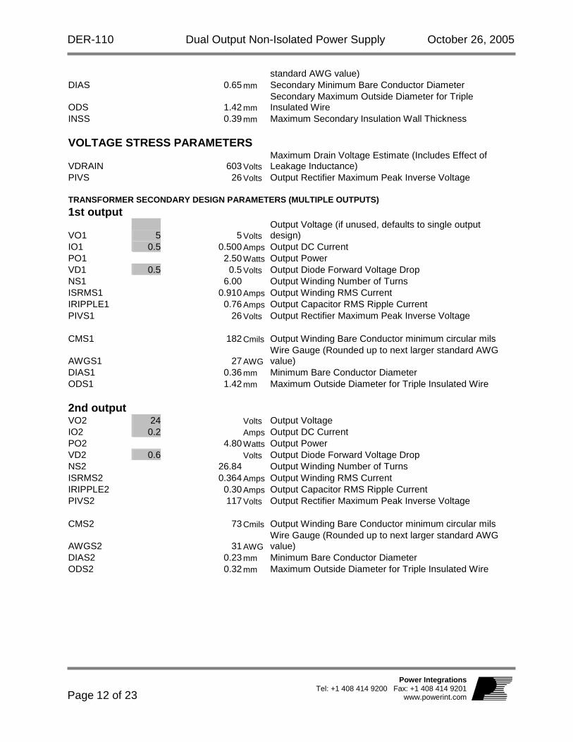
8.3 Regulation
8.3.1 Load
Figure 8 – Load Regulation @ 120VAC Input, Room Temperature
DER-110 Dual Output Non-Isolated Power Supply October 26, 2005
Page 16 of 23
Power IntegrationsTel: +1 408 414 9200 Fax: +1 408 414 9201
www.powerint.com
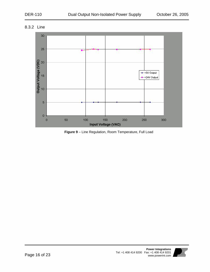
8.3.2 Line
Figure 9 – Line Regulation, Room Temperature, Full Load

DER-110 Dual Output Non-Isolated Power Supply October 26, 2005
Page 17 of 23
Power IntegrationsTel: +1 408 414 9200 Fax: +1 408 414 9201
www.powerint.com
9 Waveforms 9.1 Drain Voltage and Current, Normal Operation
Figure 10 – 85 VAC, Full Load.
Upper: IDRAIN, 0.5 A / div Lower: VDRAIN, 100 V, 2 µs / div
Figure 11 – 265 VAC, Full Load Upper: IDRAIN, 0.5 A / div Lower: VDRAIN, 200 V / div
9.2 Output Voltage Start-up Profile
Figure 12 – Start-up Profile, 90 VAC 5 ms / div.
Figure 13 – Start-up Profile, 265 VAC 5 ms / div.

DER-110 Dual Output Non-Isolated Power Supply October 26, 2005
Page 18 of 23
Power IntegrationsTel: +1 408 414 9200 Fax: +1 408 414 9201
www.powerint.com
9.3 Drain Voltage and Current Start-up Profile
Figure 14 – 85 VAC Input and Maximum Load.
Upper: IDRAIN, 0.5 A / div. Lower: VDRAIN, 100 V & 1 ms / div.
Figure 15 – 265 VAC Input and Maximum Load. Upper: IDRAIN, 0.5 A / div. Lower: VDRAIN, 200 V & 1 ms / div.
9.4 Load Transient Response (50% to 100% Load Step) In the figures shown below, signal averaging was used to better enable viewing the load transient response. The oscilloscope was triggered using the load current step as a trigger source. Since the output switching and line frequency occur essentially at random with respect to the load transient, contributions to the output ripple from these sources will average out, leaving the contribution only from the load step response.
Figure 16 – Transient Response, 90 VAC, 75-100-75% Load Step. Top: Load Current, 0.2 A/div. Bottom: Output Voltage 50 mV, 5ms / div.
Figure 17 – Transient Response, 265 VAC, 75-100-75% Load Step Upper: Load Current, 0.2 A/ div. Bottom: Output Voltage 50 mV, 5 ms / div.

DER-110 Dual Output Non-Isolated Power Supply October 26, 2005
Page 19 of 23
Power IntegrationsTel: +1 408 414 9200 Fax: +1 408 414 9201
www.powerint.com
9.5 Output Ripple Measurements
9.5.1 Ripple Measurement Technique For DC output ripple measurements, a modified oscilloscope test probe must be utilized in order to reduce spurious signals due to pickup. Details of the probe modification are provided in Figure 18 and Figure 19. The 5125BA probe adapter is affixed with two capacitors tied in parallel across the probe tip. The capacitors include one (1) 0.1 µF/50 V ceramic type and one (1) 1.0 µF/50 V aluminum electrolytic. The aluminum electrolytic type capacitor is polarized, so proper polarity across DC outputs must be maintained (see below).
Figure 18 – Oscilloscope Probe Prepared for Ripple Measurement. (End Cap and Ground Lead Removed)
Figure 19 – Oscilloscope Probe with Probe Master 5125BA BNC Adapter. (Modified with wires for probe
ground for ripple measurement, and two parallel decoupling capacitors added)
Probe Ground
Probe Tip

DER-110 Dual Output Non-Isolated Power Supply October 26, 2005
Page 20 of 23
Power IntegrationsTel: +1 408 414 9200 Fax: +1 408 414 9201
www.powerint.com
9.5.2 Measurement Results
Figure 20 – Ripple, 90 VAC, Full Load.
50us Figure 21 – Ripple, 265 VAC, Full Load.
50us

DER-110 Dual Output Non-Isolated Power Supply October 26, 2005
Page 21 of 23
Power IntegrationsTel: +1 408 414 9200 Fax: +1 408 414 9201
www.powerint.com
10 Conducted EMI A conducted EMI scan of the prototype was taken to determine the effectiveness of the input pi-filter and transformer ESHIELD® construction. The following plots show the peak performance of the converter against quasi-peak (QP) and average (AVG) limits of EN55022 Class B. Both scans were taken at 120VAC/60Hz input with maximum load applied to the outputs. Since the peak scans are below the average limits, it is expected that the QP and Average scans would have greater than 10db of margin below the limits.
Figure 22 – Conducted EMI (LINE), Maximum Load, 120 VAC, 60 Hz, and EN55022 B Limits
Figure 23 – Conducted EMI (Neutral), Maximum Load, 120 VAC, 60 Hz, and EN55022 B Limits

DER-110 Dual Output Non-Isolated Power Supply October 26, 2005
Page 22 of 23
Power IntegrationsTel: +1 408 414 9200 Fax: +1 408 414 9201
www.powerint.com
11 Revision History
Date Author Revision Description & changes Reviewed 10-26-05 RSP 1.0 Initial Release KM/JC/VC

DER-110 Dual Output Non-Isolated Power Supply October 26, 2005
Page 23 of 23
Power IntegrationsTel: +1 408 414 9200 Fax: +1 408 414 9201
www.powerint.com
For the latest updates, visit our website: www.powerint.com Power Integrations reserves the right to make changes to its products at any time to improve reliability or manufacturability. Power Integrations does not assume any liability arising from the use of any device or circuit described herein. POWER INTEGRATIONS MAKES NO WARRANTY HEREIN AND SPECIFICALLY DISCLAIMS ALL WARRANTIES INCLUDING, WITHOUT LIMITATION, THE IMPLIED WARRANTIES OF MERCHANTABILITY, FITNESS FOR A PARTICULAR PURPOSE, AND NON-INFRINGEMENT OF THIRD PARTY RIGHTS.
PATENT INFORMATION The products and applications illustrated herein (including transformer construction and circuits external to the products) may be covered by one or more U.S. and foreign patents, or potentially by pending U.S. and foreign patent applications assigned to Power Integrations. A complete list of Power Integrations’ patents may be found at www.powerint.com. Power Integrations grants its customers a license under certain patent rights as set forth at http://www.powerint.com/ip.htm. The PI Logo, TOPSwitch, TinySwitch, LinkSwitch, DPA-Switch, EcoSmart, PI Expert and PI FACTS are trademarks of Power Integrations, Inc. Other trademarks are property of their respective companies. ©Copyright 2005 Power Integrations, Inc.
Power Integrations Worldwide Sales Support Locations
WORLD HEADQUARTERS 5245 Hellyer Avenue San Jose, CA 95138, USA. Main: +1-408-414-9200 Customer Service: Phone: +1-408-414-9665 Fax: +1-408-414-9765 e-mail: [email protected]
GERMANY Rueckertstrasse 3 D-80336, Munich Germany Phone: +49-89-5527-3910 Fax: +49-89-5527-3920 e-mail: [email protected]
JAPAN Keihin Tatemono 1st Bldg 2-12-20 Shin-Yokohama, Kohoku-ku, Yokohama-shi, Kanagawa ken, Japan 222-0033 Phone: +81-45-471-1021 Fax: +81-45-471-3717 e-mail: [email protected]
TAIWAN 5F, No. 318, Nei Hu Rd., Sec. 1 Nei Hu Dist. Taipei, Taiwan 114, R.O.C. Phone: +886-2-2659-4570 Fax: +886-2-2659-4550 e-mail: [email protected]
CHINA (SHANGHAI) Rm 807-808A, Pacheer Commercial Centre, 555 Nanjing Rd. West Shanghai, P.R.C. 200041 Phone: +86-21-6215-5548 Fax: +86-21-6215-2468 e-mail: [email protected]
INDIA 261/A, Ground Floor 7th Main, 17th Cross, Sadashivanagar Bangalore, India 560080 Phone: +91-80-5113-8020 Fax: +91-80-5113-8023 e-mail: [email protected]
KOREA RM 602, 6FL Korea City Air Terminal B/D, 159-6 Samsung-Dong, Kangnam-Gu, Seoul, 135-728, Korea Phone: +82-2-2016-6610 Fax: +82-2-2016-6630 e-mail: [email protected]
EUROPE HQ 1st Floor, St. James’s House East Street, Farnham Surrey, GU9 7TJ United Kingdom Phone: +44 (0) 1252-730-140 Fax: +44 (0) 1252-727-689 e-mail: [email protected]
CHINA (SHENZHEN) Room 2206-2207, Block A, Elec. Sci. Tech. Bldg. 2070 Shennan Zhong Rd. Shenzhen, Guangdong, China, 518031 Phone: +86-755-8379-3243 Fax: +86-755-8379-5828 e-mail: [email protected]
ITALY Via Vittorio Veneto 12 20091 Bresso MI Italy Phone: +39-028-928-6000 Fax: +39-028-928-6009 e-mail: [email protected]
SINGAPORE 51 Newton Road, #15-08/10 Goldhill Plaza, Singapore, 308900 Phone: +65-6358-2160 Fax: +65-6358-2015 e-mail: [email protected]
APPLICATIONS HOTLINE World Wide +1-408-414-9660 APPLICATIONS FAX World Wide +1-408-414-9760