Embed Size (px)
Citation preview
Power Integrations
5245 Hellyer Avenue, San Jose, CA 95138 USA. Tel: +1 408 414 9200 Fax: +1 408 414 9201
www.powerint.com
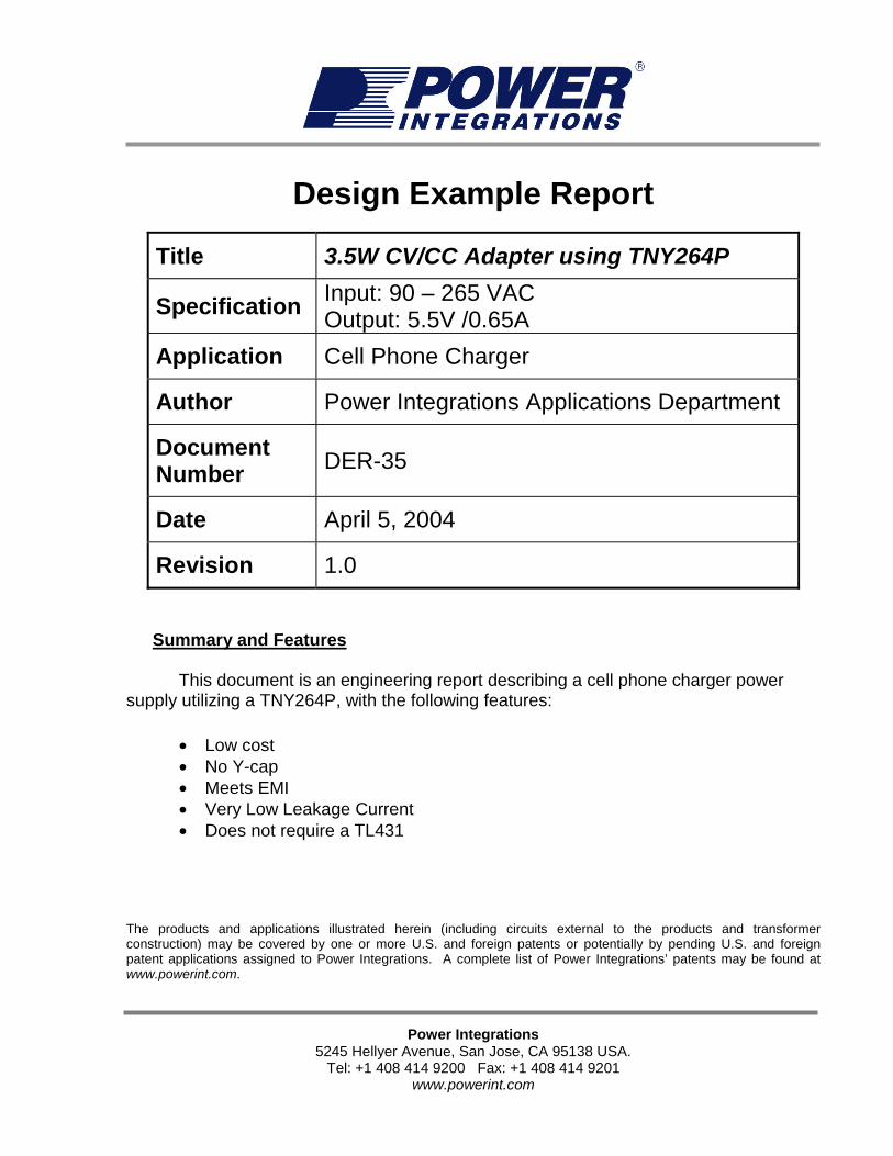
Design Example Report
Title 3.5W CV/CC Adapter using TNY264P
Specification Input: 90 – 265 VAC Output: 5.5V /0.65A
Application Cell Phone Charger
Author Power Integrations Applications Department
Document Number DER-35
Date April 5, 2004
Revision 1.0 Summary and Features
This document is an engineering report describing a cell phone charger power
supply utilizing a TNY264P, with the following features: • Low cost • No Y-cap • Meets EMI • Very Low Leakage Current • Does not require a TL431
The products and applications illustrated herein (including circuits external to the products and transformer construction) may be covered by one or more U.S. and foreign patents or potentially by pending U.S. and foreign patent applications assigned to Power Integrations. A complete list of Power Integrations’ patents may be found at www.powerint.com.
DER-35 Cell Phone Adapter TNY264 April 5, 2004
Page 2 of 22
Power IntegrationsTel: +1 408 414 9200 Fax: +1 408 414 9201
www.powerint.com
Table Of Contents 1 Introduction.................................................................................................................3 2 Power Supply Specification........................................................................................4 3 Schematic...................................................................................................................5 4 PCB Layout ................................................................................................................6 5 Bill Of Materials ..........................................................................................................7 6 Transformer Specification...........................................................................................8
6.1 Electrical Diagram...................................................................................................8 6.2 Electrical Specifications ..........................................................................................8 6.3 Materials .................................................................................................................8 6.4 Transformer Build Diagram.....................................................................................9 6.5 Transformer Construction .......................................................................................9
7 Transformer Spreadsheets.......................................................................................10 8 Performance Data ....................................................................................................12
8.1 Efficiency ..............................................................................................................12 8.2 No-load Input Power .............................................................................................13 8.3 Output Characteristic. ...........................................................................................13 8.4 Line Regulation.....................................................................................................14
9 Thermal Performance...............................................................................................15 10 Waveforms ...............................................................................................................16
10.1 Drain Voltage and Current, Normal Operation ..................................................16 10.2 Output Voltage Start-up Profile .........................................................................16 10.3 Drain Voltage and Current Start-up Profile........................................................17 10.4 Load Transient Response (75% to 100% Load Step) .......................................17 10.5 Out put Ripple Measurements...........................................................................18
10.5.1 Ripple Measurement Technique....................................................................18 10.5.2 Measurement Results....................................................................................19
11 Conducted EMI.........................................................................................................20 12 Revision History .......................................................................................................21 Important Note: Although this board is designed to satisfy safety isolation requirements, the engineering prototype has not been agency approved. Therefore, all testing should be performed using an isolation transformer to provide the AC input to the prototype board. Design Reports contain a power supply design specification, schematic, bill of materials, and transformer documentation. Performance data and typical operation characteristics are included. Typically only a single prototype has been built.
DER-35 Cell Phone Adapter TNY264 April 5, 2004
Page 3 of 22
Power IntegrationsTel: +1 408 414 9200 Fax: +1 408 414 9201
www.powerint.com
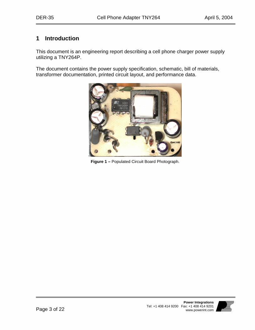
1 Introduction This document is an engineering report describing a cell phone charger power supply utilizing a TNY264P. The document contains the power supply specification, schematic, bill of materials, transformer documentation, printed circuit layout, and performance data.
Figure 1 – Populated Circuit Board Photograph.
DER-35 Cell Phone Adapter TNY264 April 5, 2004
Page 4 of 22
Power IntegrationsTel: +1 408 414 9200 Fax: +1 408 414 9201
www.powerint.com
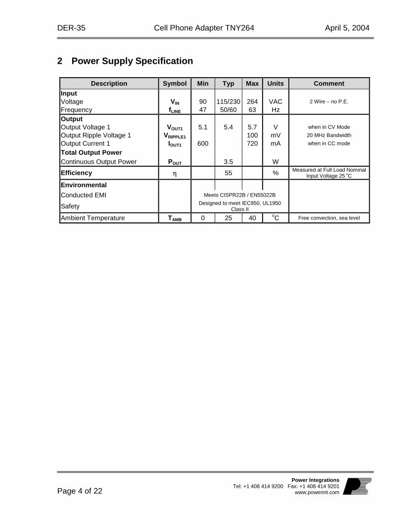
2 Power Supply Specification
Description Symbol Min Typ Max Units Comment
Input Voltage VIN 90 115/230 264 VAC 2 Wire – no P.E.
Frequency fLINE 47 50/60 63 Hz
Output
Output Voltage 1 VOUT1 5.1 5.4 5.7 V when in CV Mode
Output Ripple Voltage 1 VRIPPLE1 100 mV 20 MHz Bandwidth
Output Current 1 IOUT1 600 720 mA when in CC mode
Total Output Power
Continuous Output Power POUT 3.5 W
Efficiency η 55 % Measured at Full Load Nominal Input Voltage 25
oC
Environmental
Conducted EMI Meets CISPR22B / EN55022B
Safety Designed to meet IEC950, UL1950 Class II
Ambient Temperature TAMB 0 25 40 oC Free convection, sea level
DER-35 Cell Phone Adapter TNY264 April 5, 2004
Page 5 of 22
Power IntegrationsTel: +1 408 414 9200 Fax: +1 408 414 9201
www.powerint.com
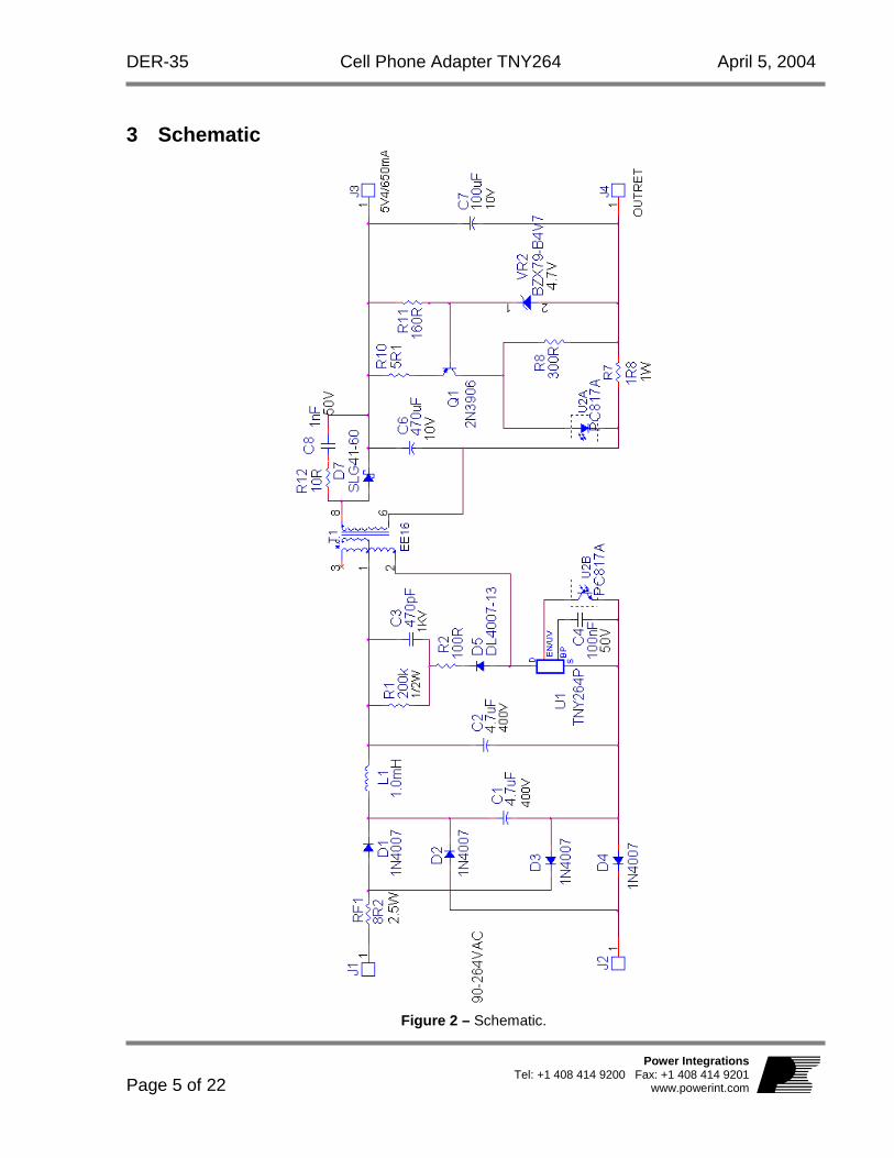
3 Schematic
Figure 2 – Schematic.
DER-35 Cell Phone Adapter TNY264 April 5, 2004
Page 6 of 22
Power IntegrationsTel: +1 408 414 9200 Fax: +1 408 414 9201
www.powerint.com
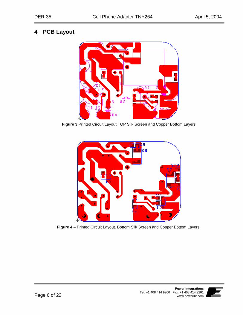
4 PCB Layout
Figure 3 Printed Circuit Layout TOP Silk Screen and Copper Bottom Layers
Figure 4 – Printed Circuit Layout. Bottom Silk Screen and Copper Bottom Layers.
DER-35 Cell Phone Adapter TNY264 April 5, 2004
Page 7 of 22
Power IntegrationsTel: +1 408 414 9200 Fax: +1 408 414 9201
www.powerint.com
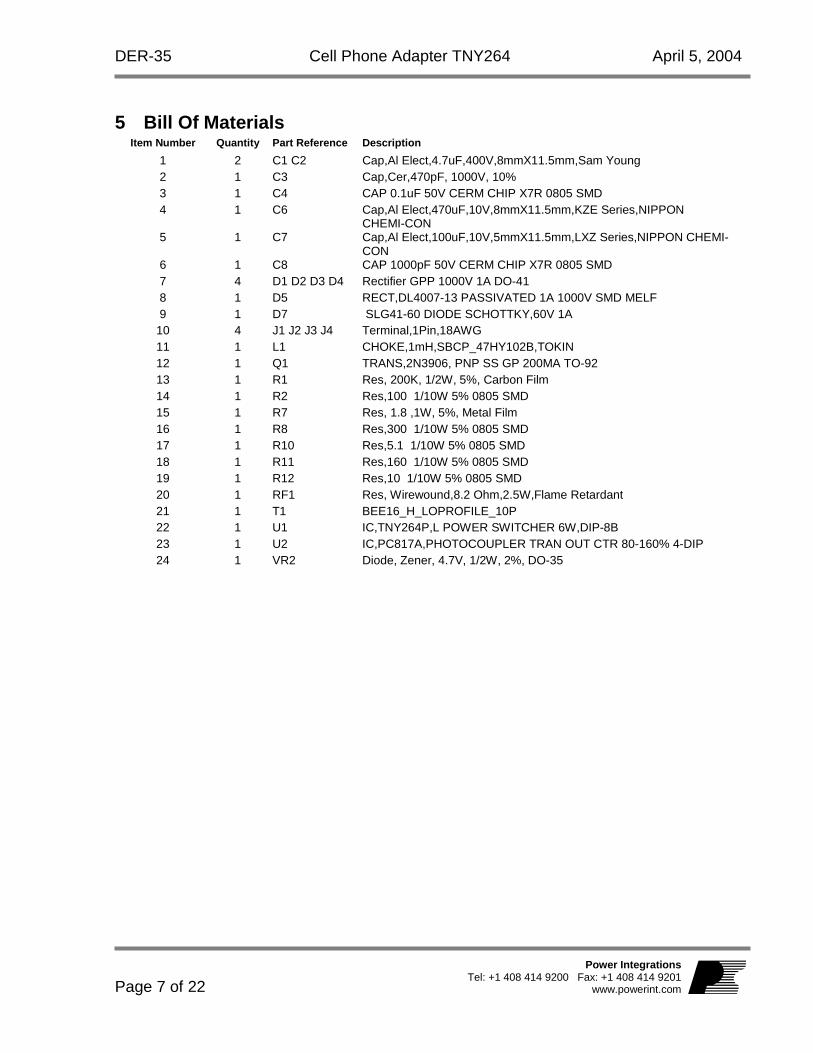
5 Bill Of Materials Item Number Quantity Part Reference Description
1 2 C1 C2 Cap,Al Elect,4.7uF,400V,8mmX11.5mm,Sam Young 2 1 C3 Cap,Cer,470pF, 1000V, 10% 3 1 C4 CAP 0.1uF 50V CERM CHIP X7R 0805 SMD 4 1 C6 Cap,Al Elect,470uF,10V,8mmX11.5mm,KZE Series,NIPPON
CHEMI-CON 5 1 C7 Cap,Al Elect,100uF,10V,5mmX11.5mm,LXZ Series,NIPPON CHEMI-
CON 6 1 C8 CAP 1000pF 50V CERM CHIP X7R 0805 SMD 7 4 D1 D2 D3 D4 Rectifier GPP 1000V 1A DO-41 8 1 D5 RECT,DL4007-13 PASSIVATED 1A 1000V SMD MELF 9 1 D7 SLG41-60 DIODE SCHOTTKY,60V 1A
10 4 J1 J2 J3 J4 Terminal,1Pin,18AWG 11 1 L1 CHOKE,1mH,SBCP_47HY102B,TOKIN 12 1 Q1 TRANS,2N3906, PNP SS GP 200MA TO-92 13 1 R1 Res, 200K, 1/2W, 5%, Carbon Film 14 1 R2 Res,100 1/10W 5% 0805 SMD 15 1 R7 Res, 1.8 ,1W, 5%, Metal Film 16 1 R8 Res,300 1/10W 5% 0805 SMD 17 1 R10 Res,5.1 1/10W 5% 0805 SMD 18 1 R11 Res,160 1/10W 5% 0805 SMD 19 1 R12 Res,10 1/10W 5% 0805 SMD 20 1 RF1 Res, Wirewound,8.2 Ohm,2.5W,Flame Retardant 21 1 T1 BEE16_H_LOPROFILE_10P 22 1 U1 IC,TNY264P,L POWER SWITCHER 6W,DIP-8B 23 1 U2 IC,PC817A,PHOTOCOUPLER TRAN OUT CTR 80-160% 4-DIP 24 1 VR2 Diode, Zener, 4.7V, 1/2W, 2%, DO-35
DER-35 Cell Phone Adapter TNY264 April 5, 2004
Page 8 of 22
Power IntegrationsTel: +1 408 414 9200 Fax: +1 408 414 9201
www.powerint.com
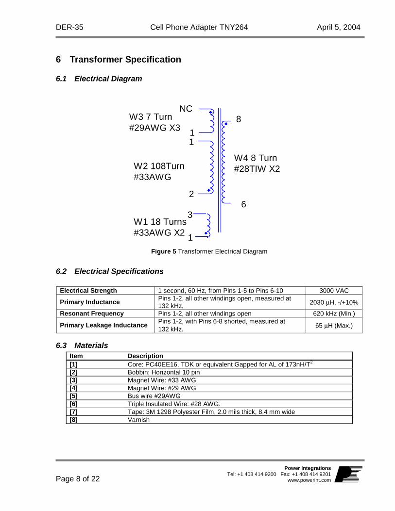
6 Transformer Specification
6.1 Electrical Diagram
1
2
8
1
W1 18 Turns#33AWG X2
W2 108Turn#33AWG
3
W3 7 Turn#29AWG X3
W4 8 Turn#28TIW X2
1
6
NC
Figure 5 Transformer Electrical Diagram
6.2 Electrical Specifications
Electrical Strength 1 second, 60 Hz, from Pins 1-5 to Pins 6-10 3000 VAC
Primary Inductance Pins 1-2, all other windings open, measured at 132 kHz, 2030 µH, -/+10%
Resonant Frequency Pins 1-2, all other windings open 620 kHz (Min.)
Primary Leakage Inductance Pins 1-2, with Pins 6-8 shorted, measured at 132 kHz. 65 µH (Max.)
6.3 Materials Item Description [1] Core: PC40EE16, TDK or equivalent Gapped for AL of 173nH/T2 [2] Bobbin: Horizontal 10 pin [3] Magnet Wire: #33 AWG [4] Magnet Wire: #29 AWG [5] Bus wire #29AWG [6] Triple Insulated Wire: #28 AWG. [7] Tape: 3M 1298 Polyester Film, 2.0 mils thick, 8.4 mm wide [8] Varnish
DER-35 Cell Phone Adapter TNY264 April 5, 2004
Page 9 of 22
Power IntegrationsTel: +1 408 414 9200 Fax: +1 408 414 9201
www.powerint.com
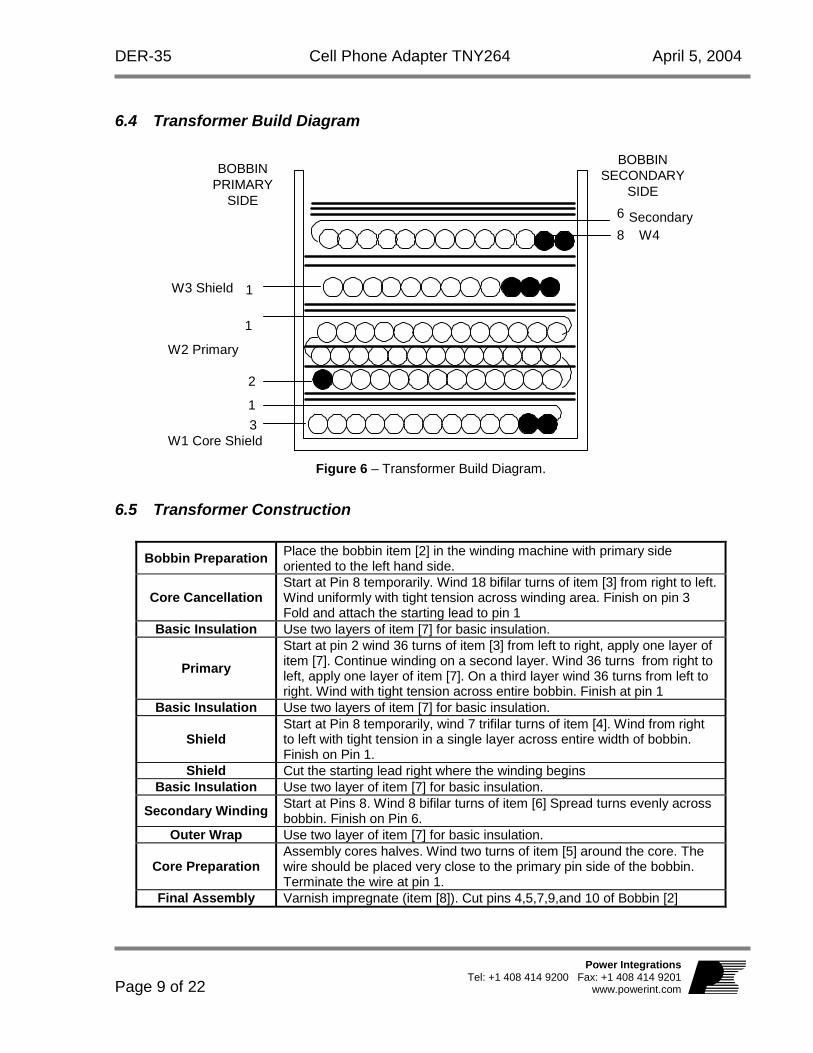
6.4 Transformer Build Diagram
1
1
W1 Core Shield
BOBBINPRIMARY
SIDE
2
BOBBINSECONDARY
SIDE
W2 Primary
W3 Shield
8 W4
6
3
Secondary
1
Figure 6 – Transformer Build Diagram.
6.5 Transformer Construction
Bobbin Preparation Place the bobbin item [2] in the winding machine with primary side oriented to the left hand side.
Core Cancellation Start at Pin 8 temporarily. Wind 18 bifilar turns of item [3] from right to left. Wind uniformly with tight tension across winding area. Finish on pin 3 Fold and attach the starting lead to pin 1
Basic Insulation Use two layers of item [7] for basic insulation.
Primary
Start at pin 2 wind 36 turns of item [3] from left to right, apply one layer of item [7]. Continue winding on a second layer. Wind 36 turns from right to left, apply one layer of item [7]. On a third layer wind 36 turns from left to right. Wind with tight tension across entire bobbin. Finish at pin 1
Basic Insulation Use two layers of item [7] for basic insulation.
Shield Start at Pin 8 temporarily, wind 7 trifilar turns of item [4]. Wind from right to left with tight tension in a single layer across entire width of bobbin. Finish on Pin 1.
Shield Cut the starting lead right where the winding begins Basic Insulation Use two layer of item [7] for basic insulation.
Secondary Winding Start at Pins 8. Wind 8 bifilar turns of item [6] Spread turns evenly across bobbin. Finish on Pin 6.
Outer Wrap Use two layer of item [7] for basic insulation.
Core Preparation Assembly cores halves. Wind two turns of item [5] around the core. The wire should be placed very close to the primary pin side of the bobbin. Terminate the wire at pin 1.
Final Assembly Varnish impregnate (item [8]). Cut pins 4,5,7,9,and 10 of Bobbin [2]
DER-35 Cell Phone Adapter TNY264 April 5, 2004
Page 10 of 22
Power IntegrationsTel: +1 408 414 9200 Fax: +1 408 414 9201
www.powerint.com
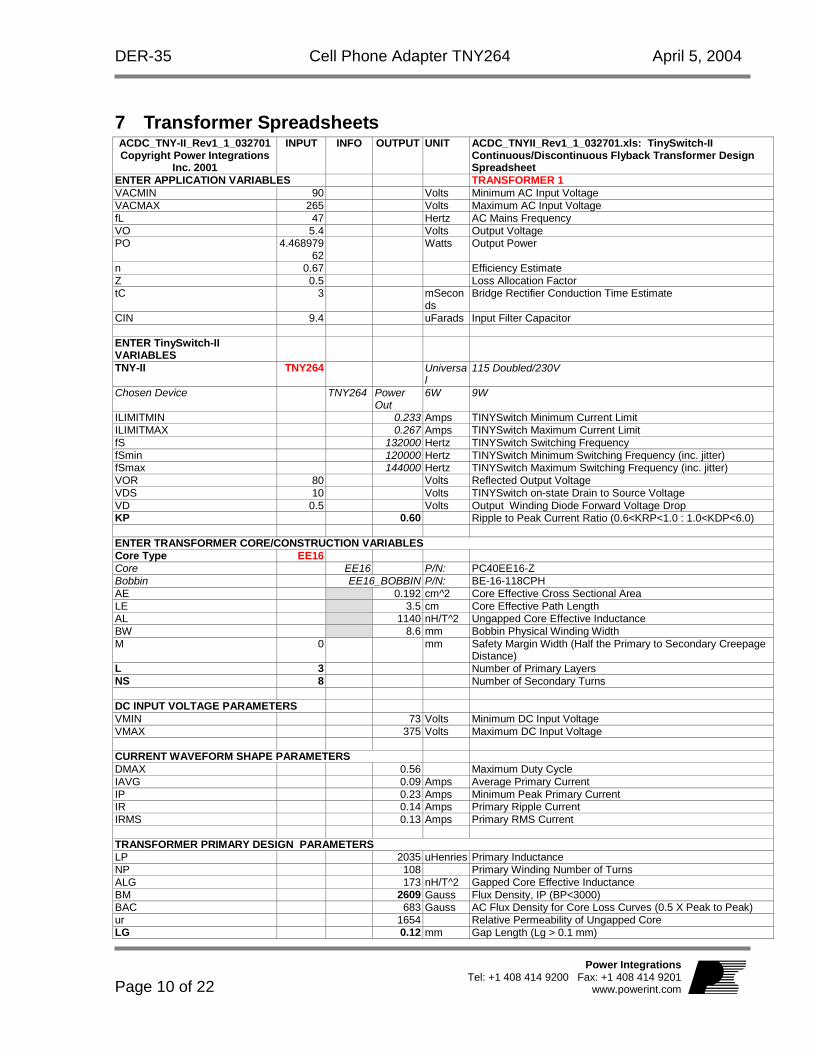
7 Transformer Spreadsheets ACDC_TNY-II_Rev1_1_032701 Copyright Power Integrations
Inc. 2001
INPUT INFO OUTPUT UNIT ACDC_TNYII_Rev1_1_032701.xls: TinySwitch-II Continuous/Discontinuous Flyback Transformer Design Spreadsheet
ENTER APPLICATION VARIABLES TRANSFORMER 1 VACMIN 90 Volts Minimum AC Input Voltage VACMAX 265 Volts Maximum AC Input Voltage fL 47 Hertz AC Mains Frequency VO 5.4 Volts Output Voltage PO 4.468979
62 Watts Output Power
n 0.67 Efficiency Estimate Z 0.5 Loss Allocation Factor tC 3 mSecon
ds Bridge Rectifier Conduction Time Estimate
CIN 9.4 uFarads Input Filter Capacitor
ENTER TinySwitch-II VARIABLES
TNY-II TNY264 Universal
115 Doubled/230V
Chosen Device TNY264 Power Out
6W 9W
ILIMITMIN 0.233 Amps TINYSwitch Minimum Current Limit ILIMITMAX 0.267 Amps TINYSwitch Maximum Current Limit fS 132000 Hertz TINYSwitch Switching Frequency fSmin 120000 Hertz TINYSwitch Minimum Switching Frequency (inc. jitter) fSmax 144000 Hertz TINYSwitch Maximum Switching Frequency (inc. jitter) VOR 80 Volts Reflected Output Voltage VDS 10 Volts TINYSwitch on-state Drain to Source Voltage VD 0.5 Volts Output Winding Diode Forward Voltage Drop KP 0.60 Ripple to Peak Current Ratio (0.6<KRP<1.0 : 1.0<KDP<6.0)
ENTER TRANSFORMER CORE/CONSTRUCTION VARIABLES Core Type EE16 Core EE16 P/N: PC40EE16-Z Bobbin EE16_BOBBIN P/N: BE-16-118CPH AE 0.192 cm^2 Core Effective Cross Sectional Area LE 3.5 cm Core Effective Path Length AL 1140 nH/T^2 Ungapped Core Effective Inductance BW 8.6 mm Bobbin Physical Winding Width M 0 mm Safety Margin Width (Half the Primary to Secondary Creepage
Distance) L 3 Number of Primary Layers NS 8 Number of Secondary Turns
DC INPUT VOLTAGE PARAMETERS VMIN 73 Volts Minimum DC Input Voltage VMAX 375 Volts Maximum DC Input Voltage
CURRENT WAVEFORM SHAPE PARAMETERS DMAX 0.56 Maximum Duty Cycle IAVG 0.09 Amps Average Primary Current IP 0.23 Amps Minimum Peak Primary Current IR 0.14 Amps Primary Ripple Current IRMS 0.13 Amps Primary RMS Current
TRANSFORMER PRIMARY DESIGN PARAMETERS LP 2035 uHenries Primary Inductance NP 108 Primary Winding Number of Turns ALG 173 nH/T^2 Gapped Core Effective Inductance BM 2609 Gauss Flux Density, IP (BP<3000) BAC 683 Gauss AC Flux Density for Core Loss Curves (0.5 X Peak to Peak) ur 1654 Relative Permeability of Ungapped Core LG 0.12 mm Gap Length (Lg > 0.1 mm)
DER-35 Cell Phone Adapter TNY264 April 5, 2004
Page 11 of 22
Power IntegrationsTel: +1 408 414 9200 Fax: +1 408 414 9201
www.powerint.com
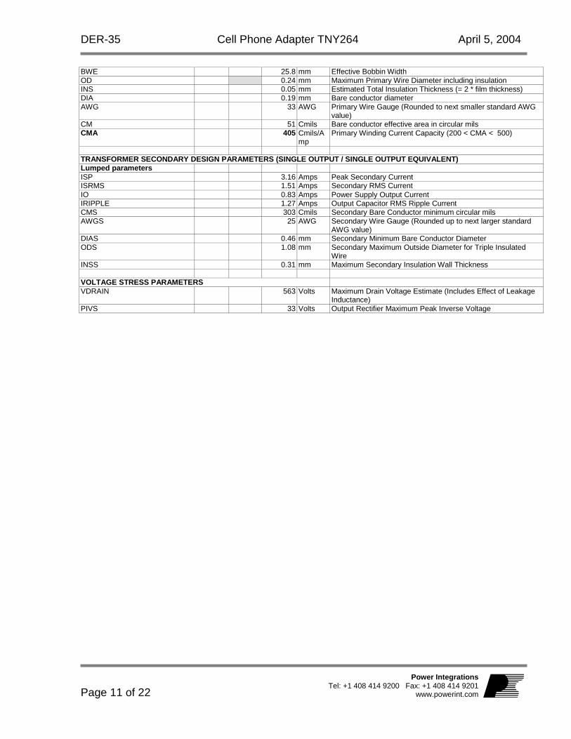
BWE 25.8 mm Effective Bobbin Width OD 0.24 mm Maximum Primary Wire Diameter including insulation INS 0.05 mm Estimated Total Insulation Thickness (= 2 * film thickness) DIA 0.19 mm Bare conductor diameter AWG 33 AWG Primary Wire Gauge (Rounded to next smaller standard AWG
value) CM 51 Cmils Bare conductor effective area in circular mils CMA 405 Cmils/A
mp Primary Winding Current Capacity (200 < CMA < 500)
TRANSFORMER SECONDARY DESIGN PARAMETERS (SINGLE OUTPUT / SINGLE OUTPUT EQUIVALENT) Lumped parameters ISP 3.16 Amps Peak Secondary Current ISRMS 1.51 Amps Secondary RMS Current IO 0.83 Amps Power Supply Output Current IRIPPLE 1.27 Amps Output Capacitor RMS Ripple Current CMS 303 Cmils Secondary Bare Conductor minimum circular mils AWGS 25 AWG Secondary Wire Gauge (Rounded up to next larger standard
AWG value) DIAS 0.46 mm Secondary Minimum Bare Conductor Diameter ODS 1.08 mm Secondary Maximum Outside Diameter for Triple Insulated
Wire INSS 0.31 mm Maximum Secondary Insulation Wall Thickness
VOLTAGE STRESS PARAMETERS VDRAIN 563 Volts Maximum Drain Voltage Estimate (Includes Effect of Leakage
Inductance) PIVS 33 Volts Output Rectifier Maximum Peak Inverse Voltage
DER-35 Cell Phone Adapter TNY264 April 5, 2004
Page 12 of 22
Power IntegrationsTel: +1 408 414 9200 Fax: +1 408 414 9201
www.powerint.com
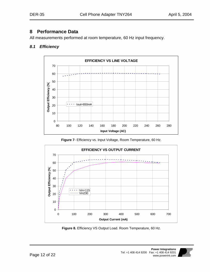
8 Performance Data All measurements performed at room temperature, 60 Hz input frequency.
8.1 Efficiency
EFFICIENCY VS LINE VOLTAGE
0
10
20
30
40
50
60
70
80 100 120 140 160 180 200 220 240 260 280
Input Voltage (AC)
Out
put
Eff
icie
ncy
(%)
Iout=650mA
Figure 7- Efficiency vs. Input Voltage, Room Temperature, 60 Hz.
EFFICIENCY VS OUTPUT CURRENT
0
10
20
30
40
50
60
70
0 100 200 300 400 500 600 700
Output Current (mA)
Out
put
Eff
icie
ncy
(%)
Vin=115Vin230
Figure 8. Efficiency VS Output Load. Room Temperature, 60 Hz.
DER-35 Cell Phone Adapter TNY264 April 5, 2004
Page 13 of 22
Power IntegrationsTel: +1 408 414 9200 Fax: +1 408 414 9201
www.powerint.com
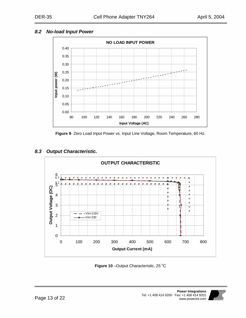
8.2 No-load Input Power
NO LOAD INPUT POWER
0.00
0.05
0.10
0.15
0.20
0.25
0.30
0.35
0.40
80 100 120 140 160 180 200 220 240 260 280
Input Voltage (AC)
Inpu
t po
wer
(W
)
Figure 9- Zero Load Input Power vs. Input Line Voltage, Room Temperature, 60 Hz.
8.3 Output Characteristic.
OUTPUT CHARACTERISTIC
5.1
5.7
0
1
2
3
4
5
6
0 100 200 300 400 500 600 700 800
Output Current (mA)
Ou
tpu
t V
olt
age
(DC
)
Vin=115VVin=230
o
Figure 10 –Output Characteristic, 25 oC
DER-35 Cell Phone Adapter TNY264 April 5, 2004
Page 14 of 22
Power IntegrationsTel: +1 408 414 9200 Fax: +1 408 414 9201
www.powerint.com
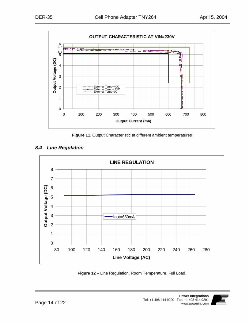
OUTPUT CHARACTERISTIC AT VIN=230V
5.1
5.7
0
1
2
3
4
5
6
0 100 200 300 400 500 600 700 800
Output Current (mA)
Out
put
Vol
tage
(D
C)
Esternal Temp=40CExternal Temp= 25CExternal Temp=0C
o
Figure 11. Output Characteristic at different ambient temperatures
8.4 Line Regulation
LINE REGULATION
0
1
2
3
4
5
6
7
8
80 100 120 140 160 180 200 220 240 260 280
Line Voltage (AC)
Ou
tpu
t V
olt
age
(DC
)
Iout=650mA
Figure 12 – Line Regulation, Room Temperature, Full Load.
DER-35 Cell Phone Adapter TNY264 April 5, 2004
Page 15 of 22
Power IntegrationsTel: +1 408 414 9200 Fax: +1 408 414 9201
www.powerint.com
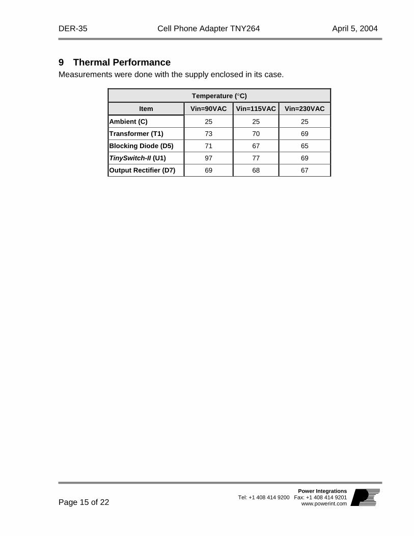
9 Thermal Performance Measurements were done with the supply enclosed in its case.
Temperature (°C)
Item Vin=90VAC Vin=115VAC Vin=230VAC
Ambient (C) 25 25 25
Transformer (T1) 73 70 69
Blocking Diode (D5) 71 67 65
TinySwitch-II (U1) 97 77 69
Output Rectifier (D7) 69 68 67
DER-35 Cell Phone Adapter TNY264 April 5, 2004
Page 16 of 22
Power IntegrationsTel: +1 408 414 9200 Fax: +1 408 414 9201
www.powerint.com
10 Waveforms
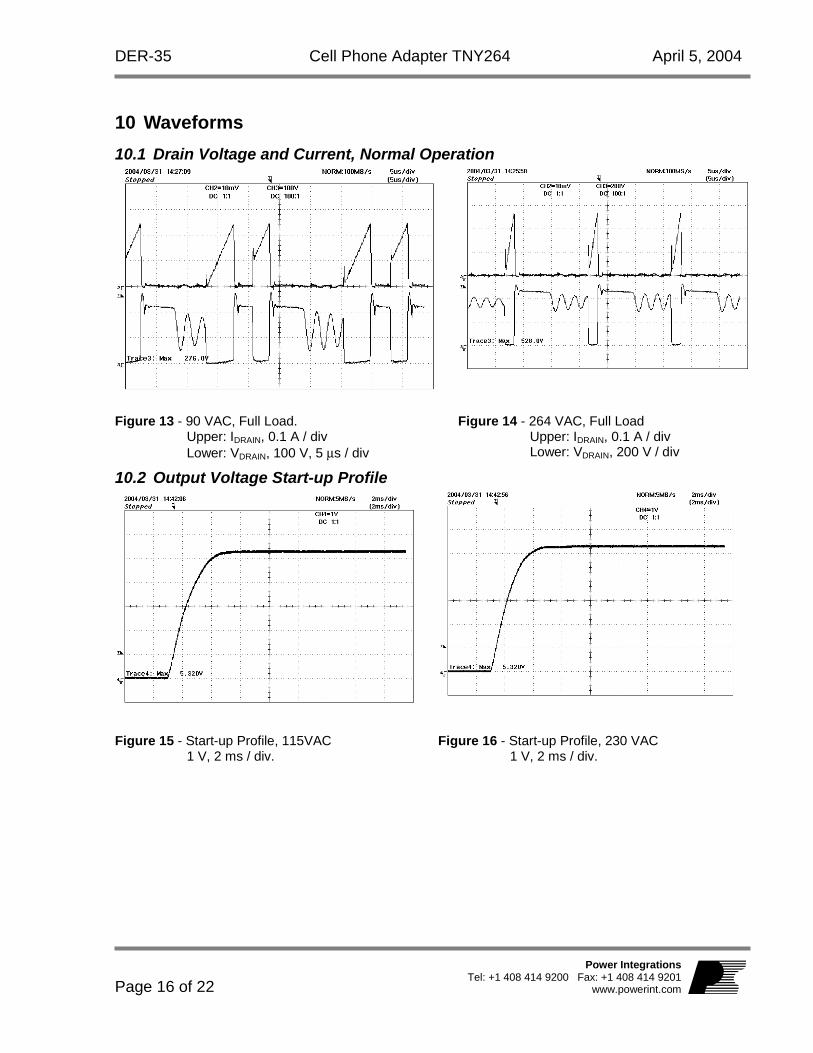
10.1 Drain Voltage and Current, Normal Operation
Figure 13 - 90 VAC, Full Load. Upper: IDRAIN, 0.1 A / div Lower: VDRAIN, 100 V, 5 µs / div
Figure 14 - 264 VAC, Full Load Upper: IDRAIN, 0.1 A / div Lower: VDRAIN, 200 V / div
10.2 Output Voltage Start-up Profile
Figure 15 - Start-up Profile, 115VAC 1 V, 2 ms / div.
Figure 16 - Start-up Profile, 230 VAC 1 V, 2 ms / div.
DER-35 Cell Phone Adapter TNY264 April 5, 2004
Page 17 of 22
Power IntegrationsTel: +1 408 414 9200 Fax: +1 408 414 9201
www.powerint.com
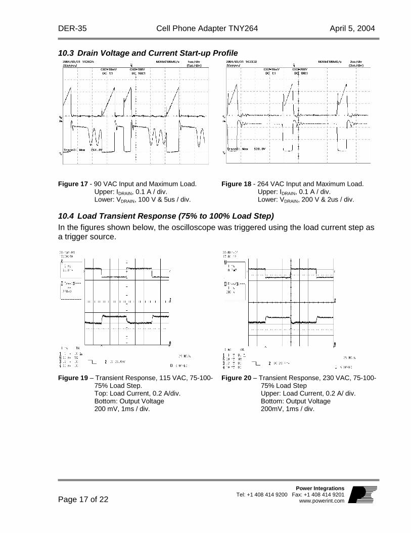
10.3 Drain Voltage and Current Start-up Profile
Figure 17 - 90 VAC Input and Maximum Load.
Upper: IDRAIN, 0.1 A / div. Lower: VDRAIN, 100 V & 5us / div.
Figure 18 - 264 VAC Input and Maximum Load. Upper: IDRAIN, 0.1 A / div. Lower: VDRAIN, 200 V & 2us / div.
10.4 Load Transient Response (75% to 100% Load Step) In the figures shown below, the oscilloscope was triggered using the load current step as a trigger source.
Figure 19 – Transient Response, 115 VAC, 75-100-
75% Load Step. Top: Load Current, 0.2 A/div. Bottom: Output Voltage 200 mV, 1ms / div.
Figure 20 – Transient Response, 230 VAC, 75-100-75% Load Step Upper: Load Current, 0.2 A/ div. Bottom: Output Voltage 200mV, 1ms / div.
DER-35 Cell Phone Adapter TNY264 April 5, 2004
Page 18 of 22
Power IntegrationsTel: +1 408 414 9200 Fax: +1 408 414 9201
www.powerint.com
10.5 Out put Ripple Measurements
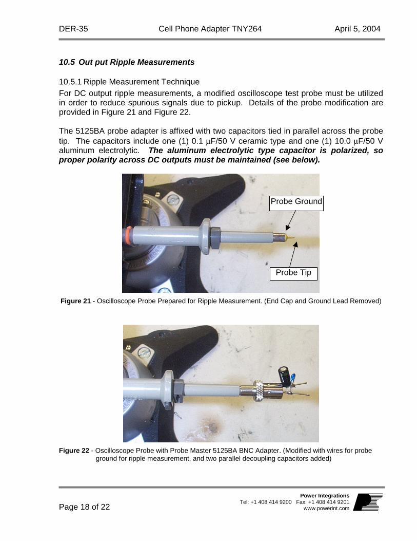
10.5.1 Ripple Measurement Technique For DC output ripple measurements, a modified oscilloscope test probe must be utilized in order to reduce spurious signals due to pickup. Details of the probe modification are provided in Figure 21 and Figure 22. The 5125BA probe adapter is affixed with two capacitors tied in parallel across the probe tip. The capacitors include one (1) 0.1 µF/50 V ceramic type and one (1) 10.0 µF/50 V aluminum electrolytic. The aluminum electrolytic type capacitor is polarized, so proper polarity across DC outputs must be maintained (see below).
Figure 21 - Oscilloscope Probe Prepared for Ripple Measurement. (End Cap and Ground Lead Removed)
Figure 22 - Oscilloscope Probe with Probe Master 5125BA BNC Adapter. (Modified with wires for probe
ground for ripple measurement, and two parallel decoupling capacitors added)
Probe Ground
Probe Tip
DER-35 Cell Phone Adapter TNY264 April 5, 2004
Page 19 of 22
Power IntegrationsTel: +1 408 414 9200 Fax: +1 408 414 9201
www.powerint.com
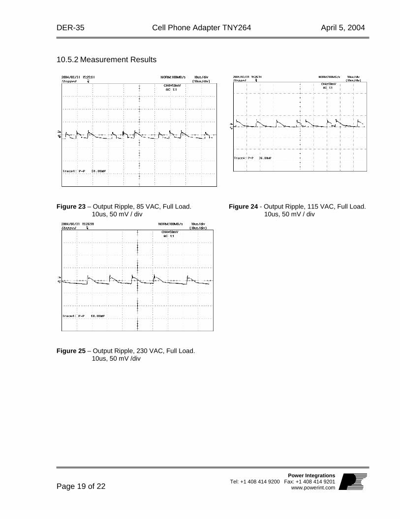
10.5.2 Measurement Results
Figure 23 – Output Ripple, 85 VAC, Full Load. 10us, 50 mV / div
Figure 24 - Output Ripple, 115 VAC, Full Load. 10us, 50 mV / div
Figure 25 – Output Ripple, 230 VAC, Full Load. 10us, 50 mV /div
DER-35 Cell Phone Adapter TNY264 April 5, 2004
Page 20 of 22
Power IntegrationsTel: +1 408 414 9200 Fax: +1 408 414 9201
www.powerint.com
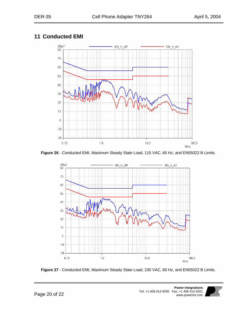
11 Conducted EMI
Figure 26 - Conducted EMI, Maximum Steady State Load, 115 VAC, 60 Hz, and EN55022 B Limits.
Figure 27 - Conducted EMI, Maximum Steady State Load, 230 VAC, 60 Hz, and EN55022 B Limits.
DER-35 Cell Phone Adapter TNY264 April 5, 2004
Page 21 of 22
Power IntegrationsTel: +1 408 414 9200 Fax: +1 408 414 9201
www.powerint.com
12 Revision History Date Author Revision Description & changes Reviewed April 5, 2004 VC 1.0 Initial release AM / VC
DER-35 Cell Phone Adapter TNY264 April 5, 2004
Page 22 of 22
Power IntegrationsTel: +1 408 414 9200 Fax: +1 408 414 9201
www.powerint.com
For the latest updates, visit our Web site: www.powerint.com Power Integrations may make changes to its products at any time. Power Integrations has no liability arising from your use of any information, device or circuit described herein nor does it convey any license under its patent rights or the rights of others. POWER INTEGRATIONS MAKES NO WARRANTIES HEREIN AND SPECIFICALLY DISCLAIMS ALL WARRANTIES INCLUDING, WITHOUT LIMITATION, THE IMPLIED WARRANTIES OF MERCHANTABILITY, FITNESS FOR A PARTICULAR PURPOSE, AND NON-INFRINGEMENT OF THIRD PARTY RIGHTS.
PATENT INFORMATION The products and applications illustrated herein (including circuits external to the products and transformer construction) may be covered by one or more U.S. and foreign patents or potentially by pending U.S. and foreign patent applications assigned to Power Integrations. A complete list of Power Integrations’ patents may be found at www.powerint.com. The PI Logo, TOPSwitch, TinySwitch, LinkSwitch, and EcoSmart are registered trademarks of Power Integrations. PI Expert and DPA-Switch are trademarks of Power Integrations. © Copyright 2004, Power Integrations.
WORLD HEADQUARTERS Power Integrations 5245 Hellyer Avenue, San Jose, CA 95138, USA Main: +1-408-414-9200 Customer Service: Phone: +1-408-414-9665 Fax: +1-408-414-9765 e-mail: [email protected]
CHINA (SHENZHEN) Power Integrations International Holdings, Inc. Rm# 1705, Bao Hua Bldg. 1016 Hua Qiang Bei Lu, Shenzhen, Guangdong, 518031, China Phone: +86-755-8367-5143 Fax: +86-755-8377-9610 e-mail: [email protected]
ITALY Power Integrations s.r.l. Via Vittorio Veneto 12, Bresso, Milano, 20091, Italy Phone: +39-028-928-6001 Fax: +39-028-928-6009 e-mail: [email protected]
SINGAPORE (ASIA PACIFIC HEADQUARTERS) Power Integrations, Singapore 51 Newton Road, #15-08/10 Goldhill Plaza, Singapore, 308900 Phone: +65-6358-2160 Fax: +65-6358-2015 e-mail: [email protected]
AMERICAS Power Integrations, Inc. 4335 South Lee Street, Suite G, Buford, GA 30518, USA Phone: +1-678-714-6033 Fax: +1-678-714-6012 e-mail: [email protected]
GERMANY Power Integrations, GmbH Rueckertstrasse 3, D-80336, Munich, Germany Phone: +49-895-527-3910 Fax: +49-895-527-3920 e-mail: [email protected]
JAPAN Power Integrations, K.K. Keihin-Tatemono 1st Bldg. 12-20 Shin-Yokohama, 2-Chome, Kohoku-ku, Yokohama-shi, Kanagawa 222-0033, Japan Phone: +81-45-471-1021 Fax: +81-45-471-3717 e-mail: [email protected]
TAIWAN Power Integrations International Holdings, Inc. 17F-3, No. 510, Chung Hsiao E. Rd., Sec. 5, Taipei, Taiwan 110, R.O.C. Phone: +886-2-2727-1221 Fax: +886-2-2727-1223 e-mail: [email protected]
CHINA (SHANGHAI) Power Integrations International Holdings, Inc. Rm 807, Pacheer, Commercial Centre, 555 Nanjing West Road, Shanghai, 200041, China Phone: +86-21-6215-5548 Fax: +86-21-6215-2468 e-mail: [email protected]
INDIA (TECHNICAL SUPPORT) Innovatech 261/A, Ground Floor 7th Main, 17th Cross, Sadashivanagar Bangalore, India, 560080 Phone: +91-80-5113-8020 Fax: +91-80-5113-8023 e-mail: [email protected]
KOREA Power Integrations International Holdings, Inc. 8th Floor, DongSung Bldg. 17-8 Yoido-dong, Youngdeungpo-gu, Seoul, 150-874, Korea Phone: +82-2-782-2840 Fax: +82-2-782-4427 e-mail: [email protected]
UK (EUROPE & AFRICA HEADQUARTERS) 1st Floor, St. James’s House East Street Farnham, Surrey GU9 7TJ United Kingdom Phone: +44-1252-730-140 Fax: +44-1252-727-689 e-mail: [email protected]
APPLICATIONS HOTLINE World Wide +1-408-414-9660
APPLICATIONS FAX World Wide +1-408-414-9760
ER or EPR template – Rev 3.4 – Single sided


![Courtly Scientists [Scienziati a Corte]brunelleschi.imss.fi.it/cimento/risorse\etesticimento.pdf · The Bifilar Pendulum.....60 9.4.3. The Pedometer](https://img.pdfslide.us/doc/110x75/5aaba38f7f8b9aa06a8c285e/courtly-scientists-scienziati-a-corte-etesticimentopdfthe-bifilar-pendulum60.jpg)