Embed Size (px)
Citation preview
Communications on Applied Electronics (CAE) – ISSN : 2394-4714
Foundation of Computer Science FCS, New York, USA
Volume 7 – No. 12, January 2018 – www.caeaccess.org
20
Design and Simulation of Single-electron Tunneling
based Nano-electronics Circuits
M. M. Abutaleb Department of Basic and Applied Sciences, Unaizah Community College, Qassim University,
Unaizah 51911, P.O. 4394, Saudi Arabia Department of Electronics, Communications and Computer Engineering, Helwan University,
Cairo, P.O. 11792, Egypt
ABSTRACT
Among various nanotechnology devices, single-electron
tunneling devices are the most promising candidates to
substitute the present CMOS devices. In this paper, a new
single-electron threshold-logic circuit module is presented for
realizing and implementing Nano-electronic circuits. The
proposed module can be dedicated to implement all basic
logic gates, such as OR, NOR, AND, NAND, XOR and
XNOR gates, that can be integrated in various manners to
design digital circuits. The simulation results demonstrate the
accuracy and stability of proposed circuit module. Design
capability and flexibility of this module are further evaluated
through the synthesis of high-level circuits.
Keywords
Nanoelectronics, SET technology, Threshold logic, Circuit
module.
1. INTRODUCTION The CMOS technology has seen tremendous growth in the
past few decades. The electronic elements scaling aims at
growing process speed and decreasing in energy used. The
scaling of CMOS devices are continuing to satisfy high
performance operation but approaching towards its limiting
size. For this issue, the electronic industry is looking for
different materials and devices to replace the existing silicon-
based CMOS devices to be used in the implementation of
circuits. There have been studies signifying that the transistor
in CMOS technology cannot shrink beyond a specified extent
dictated by the principle of its work [1-3]. These studies have
directed to investigation about promising future technologies
to increase scaling possibilities such as single-electron
tunneling, spin-stabilized magnetic, rapid single-flux-
quantum, resonant-tunneling diode and carbon-nanotube
devices [4-8].
Nanotechnology deals with the devices implementation at a
Nano-scale size that is currently challenging the entire
electronic industry in its effort to further decrease the design
of integrated circuits. Mastering of technology at this size
range has the ability to customize any doable type of materials
the way we need. The SET technology is the greatest
emerging technology accepted to meet the required features
and to replace the current CMOS technology [9-11]. SET
based devices and circuits have received enormous attention
in the research community. The SET device means the
possibility to control the place and transport of an electron
based on the quantized nature of charge. The SET circuits
have potential advantages of ultra-small size and ultra-low
power consumption [12-14]. However, most of nanoelectronic
circuits have been realized as a network of SET-based AND,
OR and NOT gates that might be severely affected by a great
circuit-depth and alternative solutions are required.
A potential alternative solution is the threshold logic gate
(TLG) based design [15-17]. The TLG-SET based circuit
design is an emerging area for development of future low
power ultra-dense Nano-electronics circuits. A number of
research works have been reported regarding the possibilities
and advantages of TLG-SET based designs and
implementations of useful logic functions [18-21]. On the
other hand, reversible logic has attractive perspective of
constructing logic circuits that are composed of connected
reversible gates to attain almost zero power dissipation
[22,23].
The main objective of this work is to present the design and
simulation of new Nano-electronic circuit module using SET
technology and threshold-logic based approach. This module
can be customized to realize basic logic gates in order to
utilize it in aspects of digital circuit design.
2. FUNDAMENTALS
2.1 SET Technology The tunnel junction and transistor are the basic elements of
single electron tunneling (SET) technology. In SET
technology, the transistor, as shown in Figure 1, contains two
SET junctions with two capacitors connected in gates. The
junction is characterized by a resistor RJ and a capacitor CJ
based on its physical design. The two SET junctions create a
quantum island that individual electrons can only arrive to it
by tunneling through one of two tunnel junctions. This
procedure is based on the tunneling effect and the Coulomb
blockade principles of single-electronics [24]. Therefore, the
charge of island can changed by transistor gates to control the
phase-shift of Coulomb oscillation as well as the single-
electron movement through a junction.
The charge transport through the SET junction is referred to
as tunneling, where the single-electron transport through this
junction is indicated as the tunnel event [9,25]. Even only
single electron tunneling may harvest an e/C voltage across
the SET junction, where C is referred to total capacitance and
e represents the electron charge (1.602x10⁻¹⁹ C). The SET
junction has the same definition of PN-junction in the
MOSFET whereas the formed island has the same definition
of MOSFET channel. Therefore the SET transistor can be
used as an electronic switch where it is pushed up into the
Coulomb blockade state as an OFF-state or else it can be
permitted to follow the current that is considered as the ON-
state.
Communications on Applied Electronics (CAE) – ISSN : 2394-4714
Foundation of Computer Science FCS, New York, USA
Volume 7 – No. 12, January 2018 – www.caeaccess.org
21
Fig 1: The schematic diagram of single-electron transistor
The need for SET-based circuit simulation has long been
recognized [26] and several simulators and simulation
methods have been developed to support SET-based circuit
design [27-30]. SIMON simulator [28] uses a combination of
the Monte Carlo method with direct calculations. The Monte
Carlo method is utilized in SECS simulator [29,30] with the
free-energy change of simulated circuit to determine the
tunnel rating of possible tunnel events, supporting thus an
actual time in the simulation of any arbitrary SET-based
circuit. In this paper, proposed SET-based circuits are
analyzing by both SECS and SIMON single-electronics
simulators.
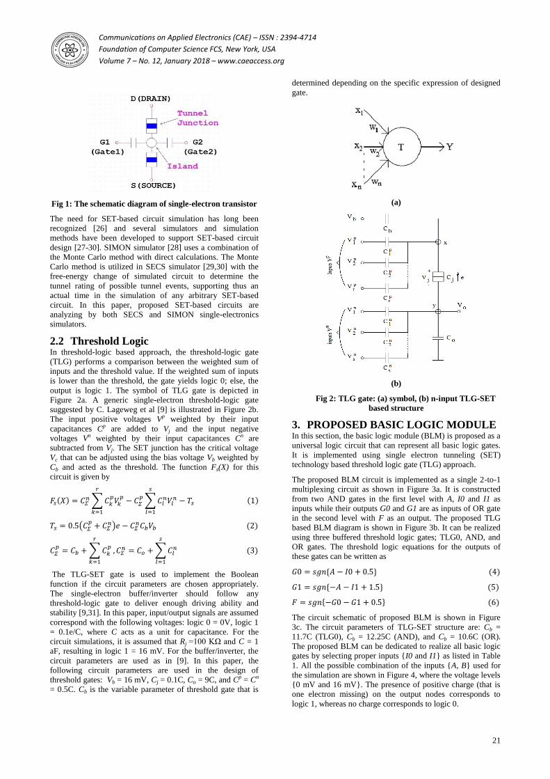
2.2 Threshold Logic In threshold-logic based approach, the threshold-logic gate
(TLG) performs a comparison between the weighted sum of
inputs and the threshold value. If the weighted sum of inputs
is lower than the threshold, the gate yields logic 0; else, the
output is logic 1. The symbol of TLG gate is depicted in
Figure 2a. A generic single-electron threshold-logic gate
suggested by C. Lageweg et al [9] is illustrated in Figure 2b.
The input positive voltages Vp weighted by their input
capacitances Cp are added to Vj and the input negative
voltages Vn weighted by their input capacitances Cn are
subtracted from Vj. The SET junction has the critical voltage
Vc that can be adjusted using the bias voltage Vb weighted by
Cb and acted as the threshold. The function Fs(X) for this
circuit is given by
The TLG-SET gate is used to implement the Boolean
function if the circuit parameters are chosen appropriately.
The single-electron buffer/inverter should follow any
threshold-logic gate to deliver enough driving ability and
stability [9,31]. In this paper, input/output signals are assumed
correspond with the following voltages: logic 0 = 0V, logic 1
= 0.1e/C, where C acts as a unit for capacitance. For the
circuit simulations, it is assumed that Rj =100 KΩ and C = 1
aF, resulting in logic 1 = 16 mV. For the buffer/inverter, the
circuit parameters are used as in [9]. In this paper, the
following circuit parameters are used in the design of
threshold gates: Vb = 16 mV, Cj = 0.1C, Co = 9C, and Cp = Cn
= 0.5C. Cb is the variable parameter of threshold gate that is
determined depending on the specific expression of designed
gate.
(a)
(b)
Fig 2: TLG gate: (a) symbol, (b) n-input TLG-SET
based structure
3. PROPOSED BASIC LOGIC MODULE In this section, the basic logic module (BLM) is proposed as a
universal logic circuit that can represent all basic logic gates.
It is implemented using single electron tunneling (SET)
technology based threshold logic gate (TLG) approach.
The proposed BLM circuit is implemented as a single 2-to-1
multiplexing circuit as shown in Figure 3a. It is constructed
from two AND gates in the first level with A, I0 and I1 as
inputs while their outputs G0 and G1 are as inputs of OR gate
in the second level with F as an output. The proposed TLG
based BLM diagram is shown in Figure 3b. It can be realized
using three buffered threshold logic gates; TLG0, AND, and
OR gates. The threshold logic equations for the outputs of
these gates can be written as
The circuit schematic of proposed BLM is shown in Figure
3c. The circuit parameters of TLG-SET structure are: Cb =
11.7C (TLG0), Cb = 12.25C (AND), and Cb = 10.6C (OR).
The proposed BLM can be dedicated to realize all basic logic
gates by selecting proper inputs {I0 and I1} as listed in Table
1. All the possible combination of the inputs {A, B} used for
the simulation are shown in Figure 4, where the voltage levels
{0 mV and 16 mV}. The presence of positive charge (that is
one electron missing) on the output nodes corresponds to
logic 1, whereas no charge corresponds to logic 0.

Communications on Applied Electronics (CAE) – ISSN : 2394-4714
Foundation of Computer Science FCS, New York, USA
Volume 7 – No. 12, January 2018 – www.caeaccess.org
22
(a)
(b)
(c)
Fig 3: Basic logic module (BLM): (a) logic diagram, (b)
TLG representation, (c) TLG-SET structure
Table 1. Basic modes of BLM
Mode
Control Pins
F(A,B) Basic Gate
I0 I1
1 1 OR
2 0 NOR
3 0 AND
4 1 NAND
5 XOR
6 XNOR
The output signals of simulated BLM-based logic gates are
also depicted in Figure 4. The simulation results represent six
modes of BLM (Table 1) that are OR(A,B), NOR(A,B),
AND(A,B), NAND(A,B), XOR(A,B), and XNOR(A,B) results,
respectively. The results obtained from the simulation are
found to be satisfactory.
Fig 4: Input and Output waveforms of dedicated BLM
circuits
The Boolean function Y is introduced in Eq. 7 as an example
for logic circuit implementation using the proposed module.
The implementation of logic function Y based on BLM is
given in Figure 5a. The blocks of BLM1, BLM2 and BLM3
are dedicated as AND, XOR and OR gates, respectively. The
complete TLG-SET schematic of designed circuit is shown in
Figure 5b. The simulation result is shown in Figure 5c for
Boolean function Y in respect to all possible input
combinations, the correct output is generated. Consequently,
the proposed module is a single-electron tunneling universal
circuit that can be utilized to implement Boolean logic
functions without needing to change its structure or
parameters of TLG-SET based design.
4. CONCLUSIONS This paper introduces a new circuit module that can be used in
the design and development of Nano-electronic circuits using
single-electron tunneling (SET) technology based threshold-
logic gate (TLG) approach. The proposed basic-logic-module
(BLM) has been used as the universal gate for implementing
all basic logic gates that can be utilized in the synthesis of
logic circuits. The performance of proposed circuit module
has been verified through SET simulations, and all results
have been found to be satisfactory. Moreover, it has been
shown that the proposed single-electron threshold-logic
building block can be configured to implement efficient high-
level circuits. Consequently, the proposed module is a good
candidate to build and develop TLG-SET based Nano-
electronic circuits without needing to change design
parameters.

Communications on Applied Electronics (CAE) – ISSN : 2394-4714
Foundation of Computer Science FCS, New York, USA
Volume 7 – No. 12, January 2018 – www.caeaccess.org
23
(a)
(b)
(c)
Fig 5: BLM-based circuit of Y function: (a) block diagram,
(b) TLG-SET layout, and (c) simulation result
5. ACKNOWLEDGEMENTS The author gratefully acknowledge Qassim University,
represented by the Deanship of Scientific Research, on the
material support for this research under the number (2105-
ucc-2016-1-12-S) during the academic year 1437-1438 AH /
2016-2017 AD.
6. REFERENCES [1] J.A. Hutchby, G.I. Bourianoff, V. V. Zhirnov, and J. E.
Brewer, “Extending the road beyond CMOS,” IEEE
Circuits Devices Mag., vol. 18, pp. 28–41, 2002.
[2] J. D. Plummer and P. B. Griffin, “Material and process
limits in silicon VLSI technology,” Proc. IEEE, vol. 89,
no. 3, pp. 240–258, 2001.
[3] D.J. Frank and Y. Taur, “Design considerations for
CMOS near the limits of scaling,” Solid–State Electron.,
vol. 46, pp. 315–320, 2002.
[4] K.K. Likharev, “Single-electron devices and their
applications,” Proc. IEEE, vol. 87, issue 4, pp. 606 -632,
1999.
[5] R. Martel, V. Derycke, J. Appenzeller et al., “Carbon
nanotube field effect transistors and logic circuits,” ACM
SIGDA DAC, 2002.
[6] O.A. Mukhanov, “Rapid single flux quantum (RSFQ)
shift register family,” IEEE Trans. on Applied
Superconductivity, vol. 3, issue 1, pp. 2578 – 2581,
1993.
[7] A.C. Seabaugh et al., “Pseudomorphic bipolar quantum
resonant tunneling transistor,” IEEE Trans. Electron
Devices, vol. 36, no. 10, pp. 2328–2334, 1989.
[8] S. Tarucha, “Shell filling and spin effects in a few
electron quantum dot,” Phys. Rev. Lett., vol. 77, pp.
3613–3616, 1996.
[9] C. Lageweg et al., “Single-electron encoded latches and
flip-flops,” IEEE Trans. Nanotechnol., vol. 3, no. 2,
2004.
[10] X.Ou and N. Wu, “Analog-digital and digital-analog
converters using single-electron and MOS transistors,”
IEEE Trans. on Nanotechnology, vol. 4, no. 6, pp 722-
729, 2005.
[11] G. Wu, L. Cai, Q. Kang, S. Wang and Q. Li, “A 8-bit
parity code generator based on multigate single electron
transistor,” IEEE NEMS, pp. 183-186, 2008.
[12] Y. C. Chen et al., “Verification of reconfigurable binary
decision diagram-based single-electron transistor arrays,”
IEEE TCAD, pp. 1473-1483, 2013.
[13] J.R. Chaudhari and D.K. Gautam, “Simulation and
analysis of hybrid ultra dense memory cell by using
single electron transistor,” IEEE ICESC, pp. 326 – 330,
2014.
[14] Y. Mizugaki, “Blocking charge oscillation in a series
array of two tiny tunnel junctions with Resistive Ground
path from its island electrode,” IEEE Trans.
Nanotechnology, vol. 11, no. 1, pp. 194-199, 2012.
[15] M. Avedillo, J. Quintana, A. Rueda, and E. Jimenez,
“Low-power CMOS threshold-logic gate,” Electric
Letters, vol. 31, pp. 2157-2159, 1995.
[16] S. Cotofana, S. Vassiliadis, “Periodic symmetric
functions, serial addition and multiplication with neural
networks,” IEEE Trans. on Neural Networks, vol. 9, no.
6, pp. 1118-1128, 1998.
[17] J. Fernandez Ramos, J. A. Hidalgo Lopez, M. J. Martin,
J. C. Tejero, A. Gago, “A threshold logic gate based on
clocked coupled inverters,” International Journal of
Electronics, vol. 84, no. 4, pp. 371-382, 1998.

Communications on Applied Electronics (CAE) – ISSN : 2394-4714
Foundation of Computer Science FCS, New York, USA
Volume 7 – No. 12, January 2018 – www.caeaccess.org
24
[18] M. M. Abutaleb, “Design and simulation of novel TLG-
SET based configurable logic cells,” Microelectron. J.,
vol. 43, issue 8, pp. 537-545, 2012.
[19] A. Ghosh, A. Jain and S. K. Sarkar, ”Design and
simulation of single electron threshold logic gate based
programmable logic array,” Procedia Technology, vol.
10, pp. 866–874, 2013.
[20] M. M. Abutaleb, “Design and simulation of novel TLG–
SET based RAM cell designs,” Microelectron. J., vol. 44,
issue 6, pp. 504-510, 2013.
[21] A. Ghosh, A. Jain, N. B.Singh and S. K. Sarkar,
“Reliability aspects and performance analysis of single
electron threshold logic based programmable logic
array”, Journal of Computational and Theoritical
Nanoscience, vol. 12, no. 9, pp. 2405- 2414, 2015.
[22] R. Landauer, “Irreversibility and heat generation in the
computational process,” IBM J. of Research and
Development, vol. 5, pp.183-191, 1961.
[23] C.H. Bennett, “Logical reversibility of computation,”
IBM J. of Research and Development, pp.525-532, 1973.
[24] C.J. Gorter, “A possible explanation of the increase of
the electrical resistance of thin metal films at low
temperatures and small field strengths,” Physica, vol. 17,
no. 8, pp. 777-780, 1951.
[25] S. Cotofana, C. Lageweg, and S. Vassilidis, “Addition
Related Arithmetic Operations via Controlled Transport
of Charge,” IEEE Trans. On Computers, vol. 54, pp.
243-256, 2005.
[26] I. Karafyllidis, “Determination of lowest energy state in
single-electron circuits,” Electron. Lett., vol. 34, pp.
2401–2403, 1998.
[27] I. Karafyllidis, “A simulator for single-electron devices
and circuits based on simulated annealing,” Superlattice.
Microstruct., vol. 25, pp. 567–572, 1999.
[28] C. Wasshuber, H. Kosina, and S. Selberherr, “SIMON—
a simulator for single-electron tunnel devices and
circuits,” IEEE Trans. Computer-Aided Design
Integrated Circuits Syst., vol. 16, pp. 937–944, 1997.
[29] G. Zardalidis and I. Karafyllidis, “Design and simulation
of a nanoelectronic single electron 2–4 decoder using a
novel simulator,” Microelectron. J., vol. 38, pp. 381–387,
2007.
[30] G. Zardalidis and I. Karafyllidis, “SECS: A New Single-
Electron-Circuit Simulator,” IEEE Transactions on
Circuits and Systems – I, vol. 55, pp. 2774-2784, 2008.
[31] C. Chen and Y. Mao, “A statistical model for single-
electron threshold logic,” IEEE trans. Electron Devices,
vol. 55, no. 6, pp. 1547-1553, 2008.