Embed Size (px)
Citation preview

Design and Observation of Biphase TiO2 Crystal with PerfectJunctionSheng-Cai Zhu, Song-Hai Xie,* and Zhi-Pan Liu*
Shanghai Key Laboratory of Molecular Catalysis and Innovative Materials, Department of Chemistry, Key Laboratory ofComputational Physical Science (Ministry of Education), Fudan University, Shanghai 200433, China
*S Supporting Information
ABSTRACT: Bicrystalline materials have wide applications from silicon chips tophotocatalysis, but the controlled synthesis of nanocrytals with ordered phase junctionhas been challenging, in particular via chemical synesthetic routes. Here, we propose ageneral strategy to design biphase crystals formed via partial solid-to-solid phase transitionwith perfect phase junction, e.g., being atomically sharp and built of two particular sets ofepitaxially joined planes of the two component phases, and present such an example bydesigning, synthesizing, and characterizing the interface of two TiO2 phases, namely, TiO2-B/anatase biphase nanocrystals that are obtained conveniently via one-pot chemicalsynthesis. Our design strategy classifies the common solid-to-solid phase transition intothree types that are distinguishable by using the newly developed stochastic surface walking(SSW) method for unbiased pathway sampling. Only Type-I crystal is predicted to possessperfect phase junction, where the phase transition involves one and only one propagationdirection featuring single pathway phase transition containing only one elementary kineticstep. The method is applicable for the understanding and the design of heterophase materials via partial phase transition ingeneral.
SECTION: Surfaces, Interfaces, Porous Materials, and Catalysis
The fabrication of bicrystalline materials has attracted muchrecent attention for their unique mechanical, optical,1 and
electrical properties.2 In photocatalysis, for example, thepresence of phase junction is also known to facilitate theseparation of the photoexcited holes and electrons and boostthe catalytic performance.3 The structurally ordered phaseboundary is important for this purpose since the defects canform charge traps and hinder the charge transfer. However, thesynthesis of high quality biphase crystalline catalysts using(in)organic wet chemical methods has been challenging, inparticular, how to control and optimize the structure of phasejunction via partial phase transition is an open question. Here,we report a general strategy to design biphase crystals withordered phase junction, e.g., lacking stacking faults or structuraldislocations, based on the newly developed SSW pathwaysampling method. This is exemplified by titania bicrystallinematerials where the atomic nature of the phase junction ischaracterized by theoretical prediction via SSW pathwaysampling and experimental observation using high-resolutiontransmission electron microscope (HRTEM).The controlled synthesis of biphase nanocrystals with
ordered interface is of great significance in photochemistry.4,5
There are various synthetic methods to achieve heterophasejunction structures, for example, via the straightforward partialsolid-to-solid phase transition and the secondary seed-growth.6−9 For the solid-to-solid phase transition, it requiresthe energetically favored phase separation and the stable phaseboundary to glue crystals together. The presence of the
structurally matched lattice or crystallographic planes isbelieved to be important to form the ordered phase junction.While the characterization of the phase junction is critical foridentifying these crystallographic planes, if present, and forunderstanding the phase transition kinetics, the interfacestructure between phases is extremely difficult to resolve,10
requiring atomic resolution at the junction experimentally and adetailed knowledge of the phase transition mechanism.In this work, we propose a general scheme, as shown in
Figure 1, to design biphase crystals via partial solid-to-solidphase transition that potentially have ordered phase junctionbased on newly developed stochastic surface walking (SSW)pathway sampling method.11−13 The SSW pathway samplingfor crystal can reveal the solid-to-solid transition pathways withexplicitly located transitions states (TS) and thus provideimportant insights into the connectivity of the crystal phases onthe potential energy surface (PES). Instead of traditional latticematching criterion, our strategy is based on the low energyphase transition pathways obtainable from SSW pathwaysampling simulation, where the energetics of the barrier heightand the complexity of the pathway (i.e., one-step, multiple-step) are the key parameters for structure prediction.Specifically, the low barrier (Ea) of the phase transformation
is desirable for achieving a stable phase junction, which is a
Received: August 2, 2014Accepted: September 2, 2014Published: September 2, 2014
Letter
pubs.acs.org/JPCL
© 2014 American Chemical Society 3162 dx.doi.org/10.1021/jz5016247 | J. Phys. Chem. Lett. 2014, 5, 3162−3168

quantitative reflection of the lattice matching (low strain) oftwo phases. However, the nature of the pathway, i.e., thedirection of the phase transition due to the anisotropy ofcrystal, could also be important. According to the complexity ofthe solid-to-solid transition pathways, we classify the common
crystal-to-crytal phase transition into three basic types (seeFigure 1) and propose a simple rule to design high qualitybiphase crystals, that is, to satisfy the Type-I phase transitioncondition, specifically, the phase transition should propagate alongone and only one direction (e.g., def ined by a habit plane),
Figure 1. Strategy to design biphase crystals with ordered phase junction via the partial solid-to-solid phase transition based on SSW crystal phasetransition pathways. Type-I crystal involves one and only one phase propagation direction often featured as a single-pathway one-step transition,which is predicted to possess ordered phase junction; Type-II crystal has multiple energetically degenerated reaction channels, and Type-III crystalhas a multiple-step phase transition mechanism involving intermediate crystal phases, both of them having more than one phase propagationdirections. The shaded areas in Type-II and Type-III crystals indicate where the stress develops during the phase junction propagation thateventually leads to large structural deformation of phase junction (e.g., cracking, stacking faults).
Figure 2. (Top panel) DFT lowest energy transition pathway from TiO2-B to anatase bulk crystal (structures viewed down from the b axis). Theblue lines indicate the habit plane of the phase transition. (Bottom panel) The atomic structure of the TiO2-B/anatase phase junction withorientation relation (2 01)B//(103)A + [010]B//[010]A as predicted from theory. From left to the right are the top-views of (103)A and (2 01)B, andtwo side-views of the junction showing the (100)B together with (001)A (theoretical dihedral angle 11.0 degrees), and (010)B//(010)A. Ti: grayballs; O: red balls.
The Journal of Physical Chemistry Letters Letter
dx.doi.org/10.1021/jz5016247 | J. Phys. Chem. Lett. 2014, 5, 3162−31683163

characterized as single pathway phase transition containing onlyone elementary kinetic step (the solid-to-solid phase transitionoccurs directly from one phase to another without any stableintermediate phases). In this way, the formed phase junctioncan be atomically sharp and built of two particular sets ofepitaxially joined planes of the two component phases. Thephase transitions along more than one propagation direction,due to the presence of either degenerate phase transitionchannels (the Type-II phase transition) or intermediate phases(the Type-III phase transition), are in principle not possible toyield biphase crystals with ordered phase junction due to theaccumulated stress at the fronts of phase boundaries. Asschematically illustrated in Figure 1, two junction fronts inType-II and Type-III crystals cannot join smoothly at thejunction−junction meeting areas (shaded in Figure 1) wherethe fracture or structural deformation (e.g., via stacking faults)is expected to develop to reduce the stress at the phaseboundaries.14,15
It should be mentioned that the heterostructured nanocryst-als with multiple phases can be synthesized by alternativetechnics other than the direct partial phase-transition, e.g., mostcommonly by heterogeneous nucleation of a secondary phaseon top of a preformed primary phase.4,6,9 These seeded-growthapproaches could also produce high quality heterointerfaces,even highly strained, for the kinetic reasons.8,9 The syntheticconditions are thus critical to the kinetics, such as the growthrate and the initial exposing facets.16 Obviously, our designstrategy does not apply to this category of phase junctions.To demonstrate this design strategy and look for the Type-I
crystal-to-crystal phase transition, we have explored the likelyphase transition pathways of TiO2 crystal using SSW,11−13
including all common TiO2 phases, e.g., rutile, anatase,brookite, and TiO2-B, without assuming any reactioncoordinates or imposing symmetry constraints. TiO2 is selectedas the example for the biphase crystal design because TiO2 hasa range of different phases, and the biphase TiO2 crystals have awide application as photocatalysts.17 Among a large data set ofphase transition pathways searched for TiO2 phases, we identifythe TiO2-B-to-antase phase transition fulfilling the Type-Icriterion. While the atomic structure of the phase junction forTiO2-B/anatase crystal is not yet determined, the main focus ofthe work is thus to characterize the phase junction using SSWsimulation and experiment to verify the theory on the biphasecrystal design. By synthesizing the TiO2-B/anatase biphasecrystals using different chemical synthetic methods, we willshow that the TiO2-B/anatase phase junction is prevalentlyperfect, i.e., free of stacking faults or defects, where the
theoretical model and experimental observation by HRTEM ishighly consistent.Taking the TiO2-B phase as the example, the crystal
extension of the SSW method (SSW-crystal) developedrecently11−13 is first utilized to sample the likely phasetransition pathways leaving TiO2-B. All calculation details aredescribed in the Supporting Information (SI) and brieflyoutlined below. The pathway sampling was carried out initiallyusing the classical Matsui−Akaogi interatomic potential18
starting from the TiO2-B phase (8 TiO2 units per cell) togenerate a database of pathways that connect TiO2-B with theother phases. In total, 4500 pathways were collected from 5000SSW-crystal steps of pathway sampling. While the majority ofthe pathways (500) were found to convert TiO2-B to anatase,the other pathways leading to the phases such as rutile werealso identified. The first-principles density functional theory(DFT) calculations based on the variable-cell double-endedsurface walking method19 were then utilized to verify theenergetics of every low energy pathways, from which the lowestenergy reaction pathway is obtained.The lowest energy pathway leaving the TiO2-B phase is the
connection between TiO2-B and anatase, which is a one-steptransition, and the other transition pathways leaving TiO2-Bphase are energetically much higher. The reaction profile isshown in Figure 2, highlighting the late TS and the smoothlattice-distortive transformation, starting from a TiO2-B lattice(a = 12.207, b = 3.769, c = 6.645 Å, α = γ = 90°, β = 75.644°)to an anatase lattice (a = 10.522, b = 3.812, c = 7.625 Å, α = γ =90°, β = 68.865°). We noticed that the TiO2-B-to-anatasepathway is much simpler compared to the anatase-to-rutilephase transition pathway, a three-step phase transition with twohigh pressure phases, MI and TiO2II, as the intermediates. Thecalculated barrier is low, only 0.12 eV per TiO2 unit from DFT,about half of that in the anatase-to-rutile phase transition,13
indicating that the TiO2-B to anatase transition is more facilecompared to the anatase-to-rutile phase transition. This wasindeed observed in experiment, where the phase transitionstarts above 673 K from TiO2-B to anatase but it is more than873 K for anatase-to-rutile.20
By closely inspecting the TiO2-B to anatase crystal transitionpathway, we can identify the habit planes of the phase transition(blue dotted line, Figure 2), being the crystal planesTiO2B(201) and anatase(103), which supports that the phasetransition basically follows the diffusionless Martensiticmechanism together with short-ranged displacement of Tiand O ions. The orientation relationship of TiO2-B/anatasephases is thus determined to be (2 01)B//(103)A + [010]B//
Figure 3. (Left) The structure and wave function of a superlattice biphase crystal, containing half−half TiO2-B/anatase phases, showing the spatiallywell separated valence band maximum (middle) and the conduction band minimum (bottom). The dotted line indicates the interface. The isosurfacedensity value of the plots is 0.02 e/bohr3. (Right) The scheme for the band alignment between TiO2-B (gray color) and anatase (green color) at thephase junction.
The Journal of Physical Chemistry Letters Letter
dx.doi.org/10.1021/jz5016247 | J. Phys. Chem. Lett. 2014, 5, 3162−31683164

[010]A. From the orientation relationship, we can construct atheoretical model for the phase junction, as shown in Figure 2.Although the habit planes, (2 01)B//(103)A, are highlycorrugated, the phase junction exhibits a closely matchedlattice and similar atomic registration between the two phases.Based on the theoretical model, a superlattice biphase crystal
comprising both TiO2-B and anatase is thus constructed andoptimized using DFT, which enables us to provide insight intothe electronic structure of the biphase crystal. Shown in Figure3 is such a biphase crystal composing half TiO2−B and halfanatase (one unit cell). Our calculation shows that the strainintroduced by the interface is very low, below 2%, and theshortest Ti−O distance at the junction is also less than 2.3%different from the bulk phases.Importantly, the TiO2−B/anatase bicrystal possesses spatially
separated valence band maximum (VMB) and conduction bandminimum (CBM), as shown in Figure 3, left. The VBM wherethe photogenerated hole resides is dominantly accumulated onthe TiO2-B side, while the CBM where the photogeneratedelectron stays is mainly populated on the anatase side.Obviously, the presence of the ordered phase junction leadsto the shrinking of band gap in the biphase crystal and a newanisotropic behavior of electron/hole transfer, that is, the holetransfers to TiO2-B while the electron goes oppositely towardanatase along the habit plane direction (Figure 3, right). This isan important optical property, which can significantly reducethe possibility for the electron−hole pair recombination andthus increase the quantum efficiency of the material.It should be mentioned that the TiO2-B/anatase system has
been studied previously by many research groups. and most ofthem obtained the phase junction via the partial phasetransition.21−27 To date, the phase junction structure at theatomic level remains unknown, and the orientation relation ishighly controversial (see SI Table S1). Two representativeorientation relations suggested recently based on HRTEMobservations are [010]A//[010]B + [001]A//[100]B reported byLi et al.23 ([uvw] represents the real space vector), and
[010]A// [010]B + (001)A//(100)B suggested by Yang et al.We found that the atomic model for the interface constructedaccording to these assignments cannot maintain the octahedronunit of Ti ions with either too close contact between Ti ions orO ions (see Figure S1 in the SI), and thus the proposedinterface atomic structures are unlikely. In fact, a very earlystudy by Brohan28 identified a(2 01)B//(103 )A orientationrelation based only on the electron diffraction pattern, andour current theoretical results are consistent with the diffractionpattern.Having the atomic structure of phase junction from theory,
we then verify the structure by experiment. Our experimentalprocedure to synthesize TiO2-B nanowire using H2Ti3O7 as theprecursor is as those described previously.29,30 The H2Ti3O7fibers can transform partially to anatase nanocrystals at thehydrothermal condition (the wet condition), and the TiO2-B/anatase bicrystalline can then be obtained after a lowtemperature (673 K) calcination.31,32 Alternatively, the TiO2-B/anatase can form directly via the solid−solid phase transitionby heating the dry TiO2-B fibers to 873 K (dry conditions),33
which is obtained from the hydrothermal synthesis. We havesynthesized the TiO2−B/anatase bicrystalline samples via bothmethods. The identity of the phases (TiO2-B and anatasecrystalline) is verified by XRD patterns, and the structure isfurther characterized using TEM and HRTEM. The exper-imental synthetic procedure and the supporting data aredetailed in the SI. Typical examples of the bicrystalline materialare shown in Figure 4a,b, where the anatase nanocrystals attachon the top of the TiO2-B nanowires. We found that bothsynthetic methods produce the same phase junction structure,being consistent at the atomic level, as revealed by HRTEM.Below we present the results for the phase junction from thesamples synthesized under wet conditions (those from dryconditions are shown in the SI).Figure 4 illustrates five different zone-axis patterns (c−g) of
HRTEM originated from two different crystals (c−e belong toone crystal, and f−g belong to another), and the important data
Figure 4. TEM (a−b) and HRTEM (c−g) images of the phase junction between anatase and TiO2-B. In the HRTEM images, c−e belong to onecrystal, and f−g belong to another. (b) The TiO2-B/anatase nanofiber and the atomic model. (c) (020)A//(020)B; (d) (011)A and (1 10)B (angle6°); (e) (004)A and (310)B (angle 48°). The theoretical structure of the junction (only showing Ti ions as blue dots) are shown in the top-rightcorner in panels d−e to compare with the experiment. (f) (11 2)A//(312 )B and (020)A//(020)B. The insert in (f) is the inverse fast Fourier transform(IFFT) of the junction area indicated by the red box, showing the perfect structure transition from one phase to another. (g): The habit planes,(103)A//(2 01)B together with (1 10)B, (011)A, and (1 12)A planes.
The Journal of Physical Chemistry Letters Letter
dx.doi.org/10.1021/jz5016247 | J. Phys. Chem. Lett. 2014, 5, 3162−31683165
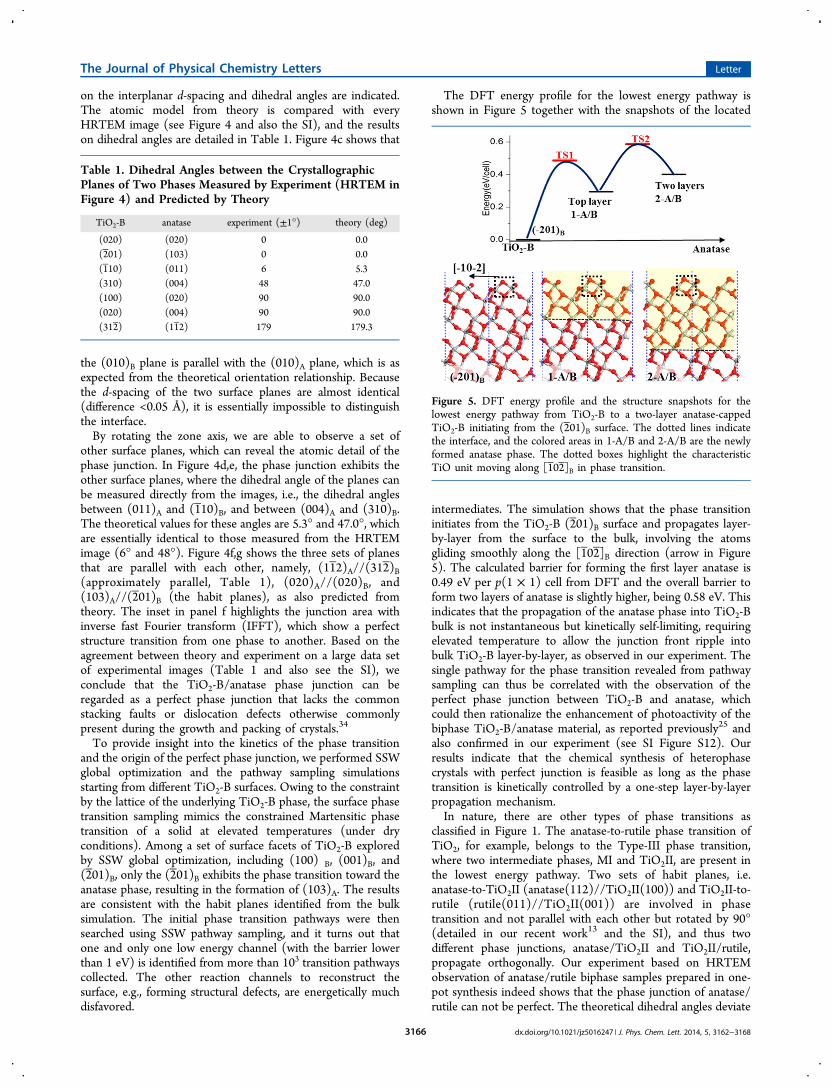
on the interplanar d-spacing and dihedral angles are indicated.The atomic model from theory is compared with everyHRTEM image (see Figure 4 and also the SI), and the resultson dihedral angles are detailed in Table 1. Figure 4c shows that
the (010)B plane is parallel with the (010)A plane, which is asexpected from the theoretical orientation relationship. Becausethe d-spacing of the two surface planes are almost identical(difference <0.05 Å), it is essentially impossible to distinguishthe interface.By rotating the zone axis, we are able to observe a set of
other surface planes, which can reveal the atomic detail of thephase junction. In Figure 4d,e, the phase junction exhibits theother surface planes, where the dihedral angle of the planes canbe measured directly from the images, i.e., the dihedral anglesbetween (011)A and (110)B, and between (004)A and (310)B.The theoretical values for these angles are 5.3° and 47.0°, whichare essentially identical to those measured from the HRTEMimage (6° and 48°). Figure 4f,g shows the three sets of planesthat are parallel with each other, namely, (11 2)A//(312 )B(approximately parallel, Table 1), (020)A//(020)B, and(103)A//(2 01)B (the habit planes), as also predicted fromtheory. The inset in panel f highlights the junction area withinverse fast Fourier transform (IFFT), which show a perfectstructure transition from one phase to another. Based on theagreement between theory and experiment on a large data setof experimental images (Table 1 and also see the SI), weconclude that the TiO2-B/anatase phase junction can beregarded as a perfect phase junction that lacks the commonstacking faults or dislocation defects otherwise commonlypresent during the growth and packing of crystals.34
To provide insight into the kinetics of the phase transitionand the origin of the perfect phase junction, we performed SSWglobal optimization and the pathway sampling simulationsstarting from different TiO2-B surfaces. Owing to the constraintby the lattice of the underlying TiO2-B phase, the surface phasetransition sampling mimics the constrained Martensitic phasetransition of a solid at elevated temperatures (under dryconditions). Among a set of surface facets of TiO2-B exploredby SSW global optimization, including (100) B, (001)B, and(201)B, only the (2 01)B exhibits the phase transition toward theanatase phase, resulting in the formation of (103)A. The resultsare consistent with the habit planes identified from the bulksimulation. The initial phase transition pathways were thensearched using SSW pathway sampling, and it turns out thatone and only one low energy channel (with the barrier lowerthan 1 eV) is identified from more than 103 transition pathwayscollected. The other reaction channels to reconstruct thesurface, e.g., forming structural defects, are energetically muchdisfavored.
The DFT energy profile for the lowest energy pathway isshown in Figure 5 together with the snapshots of the located
intermediates. The simulation shows that the phase transitioninitiates from the TiO2-B (201)B surface and propagates layer-by-layer from the surface to the bulk, involving the atomsgliding smoothly along the [1 02]B direction (arrow in Figure5). The calculated barrier for forming the first layer anatase is0.49 eV per p(1 × 1) cell from DFT and the overall barrier toform two layers of anatase is slightly higher, being 0.58 eV. Thisindicates that the propagation of the anatase phase into TiO2-Bbulk is not instantaneous but kinetically self-limiting, requiringelevated temperature to allow the junction front ripple intobulk TiO2-B layer-by-layer, as observed in our experiment. Thesingle pathway for the phase transition revealed from pathwaysampling can thus be correlated with the observation of theperfect phase junction between TiO2-B and anatase, whichcould then rationalize the enhancement of photoactivity of thebiphase TiO2-B/anatase material, as reported previously25 andalso confirmed in our experiment (see SI Figure S12). Ourresults indicate that the chemical synthesis of heterophasecrystals with perfect junction is feasible as long as the phasetransition is kinetically controlled by a one-step layer-by-layerpropagation mechanism.In nature, there are other types of phase transitions as
classified in Figure 1. The anatase-to-rutile phase transition ofTiO2, for example, belongs to the Type-III phase transition,where two intermediate phases, MI and TiO2II, are present inthe lowest energy pathway. Two sets of habit planes, i.e.anatase-to-TiO2II (anatase(112)//TiO2II(100)) and TiO2II-to-rutile (rutile(011)//TiO2II(001)) are involved in phasetransition and not parallel with each other but rotated by 90°(detailed in our recent work13 and the SI), and thus twodifferent phase junctions, anatase/TiO2II and TiO2II/rutile,propagate orthogonally. Our experiment based on HRTEMobservation of anatase/rutile biphase samples prepared in one-pot synthesis indeed shows that the phase junction of anatase/rutile can not be perfect. The theoretical dihedral angles deviate
Table 1. Dihedral Angles between the CrystallographicPlanes of Two Phases Measured by Experiment (HRTEM inFigure 4) and Predicted by Theory
TiO2-B anatase experiment (±1°) theory (deg)
(020) (020) 0 0.0(2 01) (103) 0 0.0(1 10) (011) 6 5.3(310) (004) 48 47.0(100) (020) 90 90.0(020) (004) 90 90.0(312 ) (11 2) 179 179.3
Figure 5. DFT energy profile and the structure snapshots for thelowest energy pathway from TiO2-B to a two-layer anatase-cappedTiO2-B initiating from the (2 01)B surface. The dotted lines indicatethe interface, and the colored areas in 1-A/B and 2-A/B are the newlyformed anatase phase. The dotted boxes highlight the characteristicTiO unit moving along [1 02]B in phase transition.
The Journal of Physical Chemistry Letters Letter
dx.doi.org/10.1021/jz5016247 | J. Phys. Chem. Lett. 2014, 5, 3162−31683166
from the measured values for a set of crystallographic planesfrom HRTEM by up to 13° (see SI Figure S13 for details),being much larger than that of TiO2-B/anatase samples. Thenature of the imperfect interface structure is the focus of ouronging work.The design strategy for biphase crystal presented here
establishes a fundamental connection between the “invisible”PES of crystal and the “visible” atomic structure of the phasejunction. A simple connectivity between phases, i.e., low barrier,single pathway, and one-step transition, is the key for the one-pot chemical synthesis of biphase crystals with ordered phasejunction via partial phase transition. The unbiased PESsampling using SSW methods can facilitate the understandingof the solid-to-solid phase transition and the design of newmaterials in general.
■ ASSOCIATED CONTENT*S Supporting InformationThe SSW-crystal pathway sampling method and the calculationdetail; the experimental procedure to synthesize biphasecrystals and the experimental data (XRD, HRTEM) forcharacterizing the biphase crystals prepared at the dryconditions; the HRTEM results on the phase junction ofrutile/anatase; and the photoactivity test of TiO2−B/anatasebiphase sample. This material is available free of charge via theInternet at http://pubs.acs.org.
■ AUTHOR INFORMATIONCorresponding Authors*E-mail: [email protected] (S.H.X.).*E-mail: [email protected] (Z.P.L.).
NotesThe authors declare no competing financial interest.
■ ACKNOWLEDGMENTSThis work is supported by the National Science Foundation ofChina (21173051 , 21361130019) , 973 program(2011CB808500, 2013CB834603), the Science and Technol-ogy Commission of Shanghai Municipality (08DZ2270500),and the Program for Professor of Special Appointment (EasternScholar) at Shanghai Institute of Higher Learning.
■ REFERENCES(1) Kawahara, T.; Konishi, Y.; Tada, H.; Tohge, N.; Nishii, J.; Ito, S.A Patterned TiO2 (Anatase)/TiO2 (Rutile) Bilayer-Type Photo-catalyst: Effect of the Anatase/Rutile Junction on the PhotocatalyticActivity. Angew. Chem. 2002, 114, 2935−2937.(2) Chiang, Y. M.; Silverman, L. A.; French, R. H.; Cannon, R. M.Thin Glass Film between Ultrafine Conductor Particles in Thick-FilmResistors. J. Am. Ceram. Soc. 1994, 77, 1143−1152.(3) Zhang, J.; Xu, Q.; Feng, Z.; Li, M.; Li, C. Importance of theRelationship between Surface Phases and Photocatalytic Activity ofTiO2. Angew. Chem., Int. Ed. 2008, 47, 1766−1769.(4) Hurum, D.; Agrios, A.; Crist, S.; Gray, K.; Rajh, T.; Thurnauer,M. Probing Reaction Mechanisms in Mixed Phase TiO2 by EPR. J.Electron Spectrosc. Relat. Phenom. 2006, 150, 155−163.(5) Yang, D. J.; Liu, H. W.; Zheng, Z. F.; Yuan, Y.; Zhao, J. C.;Waclawik, E. R.; Ke, X. B.; Zhu, H. Y. An Efficient PhotocatalystStructure: TiO2(B) Nanofibers with a Shell of Anatase Nanocrystals. J.Am. Chem. Soc. 2009, 131, 17885−17893.(6) Carbone, L.; Cozzoli, P. D. Colloidal HeterostructuredNanocrystals: Synthesis and Growth Mechanisms. Nano Today2010, 5, 449−493.
(7) Casavola, M.; Buonsanti, R.; Caputo, G.; Cozzoli, P. D. ColloidalStrategies for Preparing Oxide-Based Hybrid Nanocrystals. Eur. J.Inorg. Chem. 2008, 837−854.(8) Buonsanti, R.; Grillo, V.; Carlino, E.; Giannini, C.; Gozzo, F.;Garcia-Hernandez, M.; Garcia, M. A.; Cingolani, R.; Cozzoli, P. D.Architectural Control of Seeded-Grown Magnetic-Semicondutor IronOxide−TiO2 Nanorod Heterostructures: The Role of Seeds inTopology Selection. J. Am. Chem. Soc. 2010, 132, 2437−2464.(9) Buonsanti, R.; Grillo, V.; Carlino, E.; Giannini, C.; Curri, M. L.;Innocenti, C.; Sangregorio, C.; Achterhold, K.; Parak, F. G.; Agostiano,A.; et al. Seeded Growth of Asymmetric Binary Nanocrystals Made ofa Semiconductor TiO2 Rodlike Section and a Magnetic Gamma-Fe2O3
Spherical Domain. J. Am. Chem. Soc. 2006, 128, 16953−16970.(10) Chua, A. L.-S.; Benedek, N. A.; Chen, L.; Finnis, M. W.; Sutton,A. P. A Genetic Algorithm for Predicting the Structures of Interfaces inMulticomponent Systems. Nat. Mater. 2010, 9, 418−422.(11) Shang, C.; Liu, Z.-P. Stochastic Surface Walking Method forStructure Prediction and Pathway Searching. J. Chem. Theory Comput.2013, 9, 1838−1845.(12) Zhang, X.-J.; Shang, C.; Liu, Z.-P. From Atoms to Fullerene:Stochastic Surface Walking Solution for Automated StructurePrediction of Complex Material. J. Chem. Theory Comput. 2013, 9,3252−3260.(13) Shang, C.; Zhang, X.-J.; Liu, Z.-P. Stochastic Surface WalkingMethod for Crystal Structure and Phase Transition PathwayPrediction. Phys. Chem. Chem. Phys. 2014, 16, 17845.(14) Capolungo, L.; Spearot, D.; Cherkaoui, M.; McDowell, D.; Qu,J.; Jacob, K. Dislocation Nucleation from Bicrystal Interfaces and Grainboundary Ledges: Relationship to Nanocrystalline Deformation. J.Mech. Phys. Solids 2007, 55, 2300−2327.(15) Gilbert, B.; Huang, F.; Zhang, H.; Waychunas, G. A.; Banfield, J.F. Nanoparticles: Strained and Stiff. Science 2004, 305, 651−654.(16) Shim, M.; McDaniel, H. Anisotropic Nanocrystal Hetero-structures: Synthesis and Lattice Strain. Curr. Opin. Solid State Mater.Sci. 2010, 14, 83−94.(17) Gratzel, M. Photoelectrochemical Cells. Nature 2001, 414, 338−344.(18) Matsui, M.; Akaogi, M. Molecular Dynamics Simulation of theStructural and Physical Properties of the Four Polymorphs of TiO2.Mol. Simul. 1991, 6, 239−244.(19) Zhang, X. J.; Shang, C.; Liu, Z. P. Double-Ended SurfaceWalking Method for Pathway Building and Transition State Locationof Complex Reactions. J. Chem. Theory Comput. 2013, 9, 5745−5753.(20) Zhang, H.; Banfield, J. F. New Kinetic Model for theNanocrystalline Anatase-to-Rutile Transformation Revealing RateDependence on Number of Particles. Am. Mineral. 1999, 84, 528−535.(21) Liu, B.; Khare, A.; Aydil, E. S. TiO2-B/Anatase Core-ShellHeterojunction Nanowires for Photocatalysis. ACS Appl. Mater.Interfaces 2011, 3, 4444−4450.(22) Yoshida, R.; Suzuki, Y.; Yoshikawa, S. Syntheses of TiO2(B)Nanowires and TiO2 Anatase Nanowires by Hydrothermal and Post-heat Treatments. J. Solid State Chem. 2005, 178, 2179−2185.(23) Li, W.; Liu, C.; Zhou, Y.; Bai, Y.; Feng, X.; Yang, Z.; Lu, L.; Lu,X.; Chan, K.-Y. Enhanced Photocatalytic Activity in Anatase/TiO2(B)Core−Shell Nanofiber. J. Phys. Chem. C 2008, 112, 20539−20545.(24) Bai, Y.; Li, W.; Liu, C.; Yang, Z. H.; Feng, X.; Lu, X. H.; Chan,K. Y. Stability of Pt Nanoparticles and Enhanced PhotocatalyticPerformance in Mesoporous Pt-(Anatase/TiO2(B) Nanoarchitecture.J. Mater. Chem. 2009, 19, 7055−7061.(25) Zhou, W. J.; Gai, L. G.; Hu, P. G.; Cui, J. J.; Liu, X. Y.; Wang, D.Z.; Li, G. H.; Jiang, H. D.; Liu, D.; Liu, H.; et al. Phase Transformationof TiO2 Nanobelts and TiO2(B)/Anatase Interface HeterostructureNanobelts with Enhanced Photocatalytic Activity. CrystEngComm2011, 13, 6643−6649.(26) Zheng, Z. F.; Liu, H. W.; Ye, J. P.; Zhao, J. C.; Waclawik, E. R.;Zhu, H. Y. Structure and Contribution to Photocatalytic Activity of theInterfaces in Nanofibers with Mixed Anatase and TiO2(B) Phases. J.Mol. Catal. A: Chem. 2010, 316, 75−82.
The Journal of Physical Chemistry Letters Letter
dx.doi.org/10.1021/jz5016247 | J. Phys. Chem. Lett. 2014, 5, 3162−31683167

(27) Huang, C. X.; Zhu, K. R.; Qi, M. Y.; Zhuang, Y. L.; Cheng, C.Preparation and Photocatalytic Activity of Bicrystal Phase TiO2Nanotubes Containing TiO2-B and Anatase. J. Phys. Chem. Solids2012, 73, 757−761.(28) Brohan, L.; Verbaere, A.; Tournoux, M.; Demazeau, G. LaTransformation TiO2(B)→ Anatase. Mater. Res. Bull. 1982, 17, 355−361.(29) Armstrong, A. R.; Armstrong, G.; Canales, J.; Bruce, P. G. TiO2-B Nanowires. Angew. Chem., Int. Ed. Engl. 2004, 43, 2286−8.(30) Armstrong, A. R.; Armstrong, G.; Canales, J.; García, R.; Bruce,P. G. Lithium-Ion Intercalation into TiO2-B Nanowires. Adv. Mater.2005, 17, 862−865.(31) Zhu, H.; Gao, X.; Lan, Y.; Song, D.; Xi, Y.; Zhao, J. HydrogenTitanate Nanofibers Covered with Anatase Nanocrystals: A DelicateStructure Achieved by the Wet Chemistry Reaction of the TitanateNanofibers. J. Am. Chem. Soc. 2004, 126, 8380−8381.(32) Tsai, C. C.; Teng, H. S. Structural Features of NanotubesSynthesized from NaOH Treatment on TiO2 with Different Post-treatments. Chem. Mater. 2006, 18, 367−373.(33) Kuo, H.-L.; Kuo, C.-Y.; Liu, C.-H.; Chao, J.-H.; Lin, C.-H. AHighly Active Bi-crystalline Photocatalyst Consisting of TiO2(B)Nanotube and Anatase Particle for Producing H2 Gas from NeatEthanol. Catal. Lett. 2007, 113, 7−12.(34) Penn, R. L. Imperfect Oriented Attachment: DislocationGeneration in Defect-Free Nanocrystals. Science 1998, 281, 969−971.
The Journal of Physical Chemistry Letters Letter
dx.doi.org/10.1021/jz5016247 | J. Phys. Chem. Lett. 2014, 5, 3162−31683168