Embed Size (px)
Citation preview
1Dept.: System Design & IntegrationRF & High-Speed System Design GroupHead of Group: Dr.-Ing. Ivan Ndip
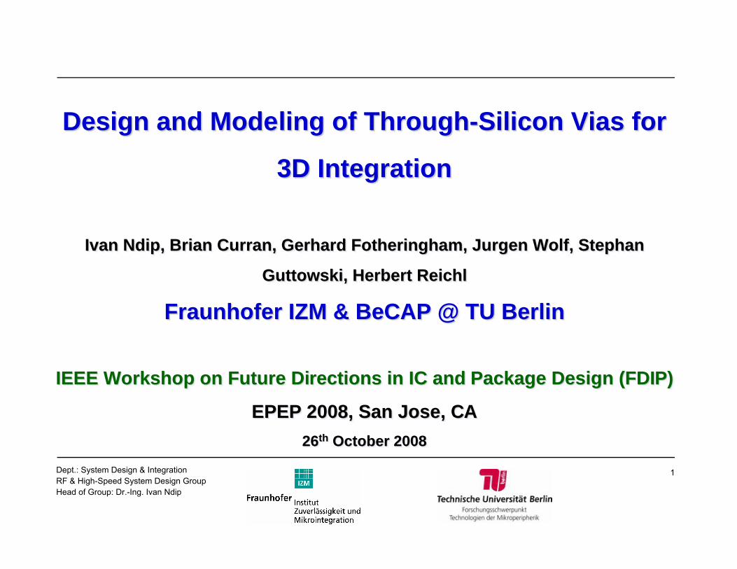
Design and Modeling of Through-Silicon Vias for
3D Integration
Ivan Ndip, Brian Curran, Gerhard Fotheringham, Jurgen Wolf, Stephan
Guttowski, Herbert Reichl
Fraunhofer IZM & BeCAP @ TU Berlin
IEEE Workshop on Future Directions in IC and Package Design (FDIP)
EPEP 2008, San Jose, CA
26th October 2008
Design and Modeling of ThroughDesign and Modeling of Through--Silicon Vias for Silicon Vias for
3D Integration3D Integration
Ivan Ndip, Brian Curran, Gerhard Fotheringham, Jurgen Wolf, StepIvan Ndip, Brian Curran, Gerhard Fotheringham, Jurgen Wolf, Stephan han
Guttowski, Herbert ReichlGuttowski, Herbert Reichl
Fraunhofer IZM & BeCAP @ TU BerlinFraunhofer IZM & BeCAP @ TU Berlin
IEEE Workshop on Future Directions in IC and Package Design (FDIIEEE Workshop on Future Directions in IC and Package Design (FDIP)P)
EPEP 2008, San Jose, CA EPEP 2008, San Jose, CA
2626thth October 2008October 2008
2Dept.: System Design & IntegrationRF & High-Speed System Design GroupHead of Group: Dr.-Ing. Ivan Ndip
■ Motivation
■ Quantification of Some EMR Problems caused by TSVs
■ Methods for Enhancing RF Performance of TSVs in Low Resistivity Silicon
■ On-going Activities to Overcome TSV Design & Fabrication Challenges
Outline
3Dept.: System Design & IntegrationRF & High-Speed System Design GroupHead of Group: Dr.-Ing. Ivan Ndip
■ Motivation
■ Quantification of Some EMR Problems caused by TSVs
■ Methods for Enhancing RF Performance of TSVs in Low Resistivity Silicon
■ On-going Activities to Overcome TSV Design & Fabrication Challenges
Outline
4Dept.: System Design & IntegrationRF & High-Speed System Design GroupHead of Group: Dr.-Ing. Ivan Ndip
Motivation – 1/2
■ To meet consumer demands for miniaturized, high-performance and low-cost products, 3D chip-stacked packages are needed.
■ TSVs offer many advantages over conventional bonding techniques in facilitating 3D integration.
■ A range of applications are emerging in which TSVs will be implemented to develop stacked and miniaturized electronic systems.
5Dept.: System Design & IntegrationRF & High-Speed System Design GroupHead of Group: Dr.-Ing. Ivan Ndip
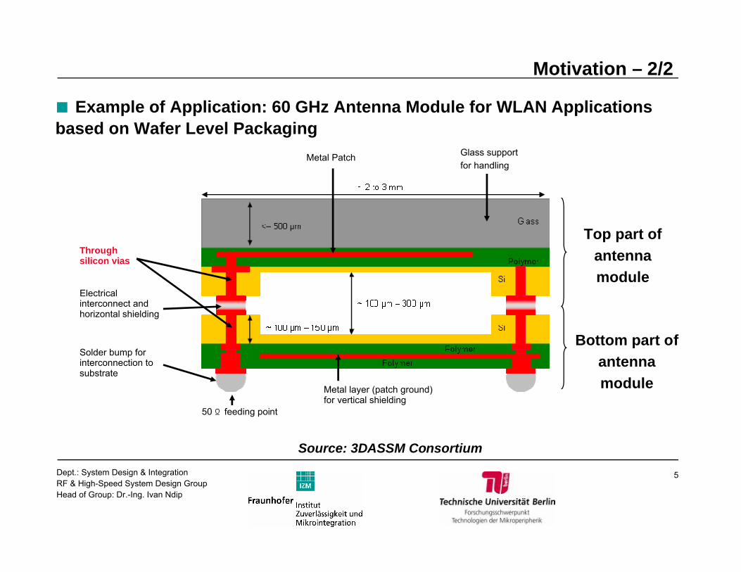
Top part of
antenna
module
Bottom part of
antenna
moduleMetal layer (patch ground) for vertical shielding
50 Ω feeding point
Solder bump for interconnection to substrate
Electrical interconnect and horizontal shielding
Through silicon vias
Glass support
for handlingMetal Patch
Source: 3DASSM Consortium
Motivation – 2/2
■ Example of Application: 60 GHz Antenna Module for WLAN Applications based on Wafer Level Packaging
6Dept.: System Design & IntegrationRF & High-Speed System Design GroupHead of Group: Dr.-Ing. Ivan Ndip
■ Motivation
■ Quantification of Some EMR Problems caused by TSVs
■ Methods for Enhancing RF Performance of TSVs in Low Resistivity Silicon
■ On-going Activities to Overcome TSV Design & Fabrication Challenges
Outline
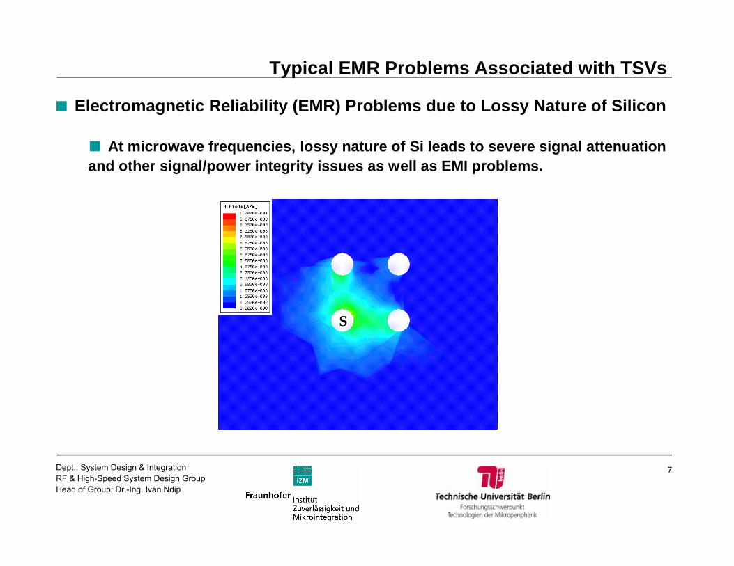
7Dept.: System Design & IntegrationRF & High-Speed System Design GroupHead of Group: Dr.-Ing. Ivan Ndip
■ Electromagnetic Reliability (EMR) Problems due to Lossy Nature of Silicon
■ At microwave frequencies, lossy nature of Si leads to severe signal attenuation and other signal/power integrity issues as well as EMI problems.
Typical EMR Problems Associated with TSVs
S
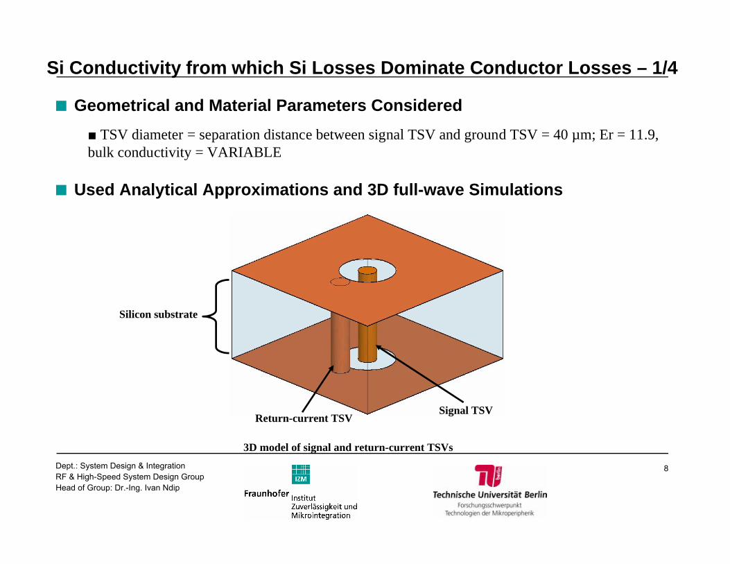
8Dept.: System Design & IntegrationRF & High-Speed System Design GroupHead of Group: Dr.-Ing. Ivan Ndip
■ Geometrical and Material Parameters Considered
■ TSV diameter = separation distance between signal TSV and ground TSV = 40 µm; Er = 11.9, bulk conductivity = VARIABLE
■ Used Analytical Approximations and 3D full-wave Simulations
Si Conductivity from which Si Losses Dominate Conductor Losses – 1/4
Return-current TSVSignal TSV
Silicon substrate
3D model of signal and return-current TSVs
9Dept.: System Design & IntegrationRF & High-Speed System Design GroupHead of Group: Dr.-Ing. Ivan Ndip
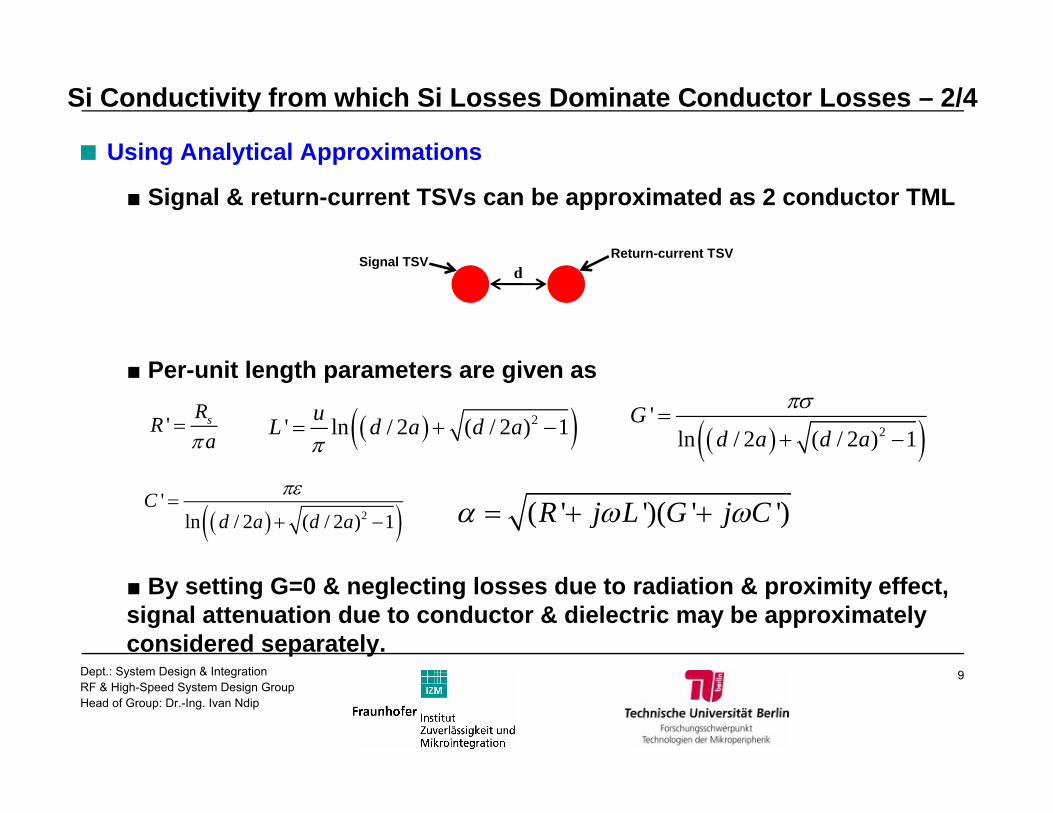
■ Using Analytical Approximations
■ Signal & return-current TSVs can be approximated as 2 conductor TML
■ Per-unit length parameters are given as
■ By setting G=0 & neglecting losses due to radiation & proximity effect, signal attenuation due to conductor & dielectric may be approximately considered separately.
Signal TSV
( ' ')( ' ')R j L G j C
' sRR
a 2' ln / 2 ( / 2 ) 1
uL d a d a
2
'ln / 2 ( / 2 ) 1
Gd a d a
2'
ln / 2 ( / 2 ) 1C
d a d a
dReturn-current TSV
Si Conductivity from which Si Losses Dominate Conductor Losses – 2/4
10Dept.: System Design & IntegrationRF & High-Speed System Design GroupHead of Group: Dr.-Ing. Ivan Ndip
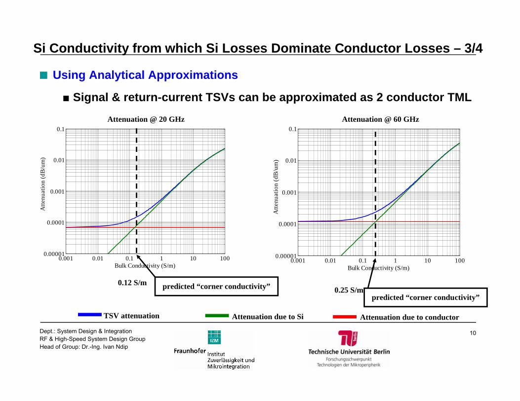
Attenuation due to Si Attenuation due to conductorTSV attenuation
0.001 0.01 0.1 1 10 1000.00001
0.0001
0.001
0.01
0.1
Bulk Conductivity (S/m)
Att
enua
tion
(dB
/um
)
0.001 0.01 0.1 1 10 1000.00001
0.0001
0.001
0.01
0.1
Bulk Conductivity (S/m)A
tten
uati
on (
dB/u
m)
Attenuation @ 20 GHz
0.12 S/m predicted “corner conductivity”
Attenuation @ 60 GHz
0.25 S/mpredicted “corner conductivity”
■ Using Analytical Approximations
■ Signal & return-current TSVs can be approximated as 2 conductor TML
Si Conductivity from which Si Losses Dominate Conductor Losses – 3/4
11Dept.: System Design & IntegrationRF & High-Speed System Design GroupHead of Group: Dr.-Ing. Ivan Ndip
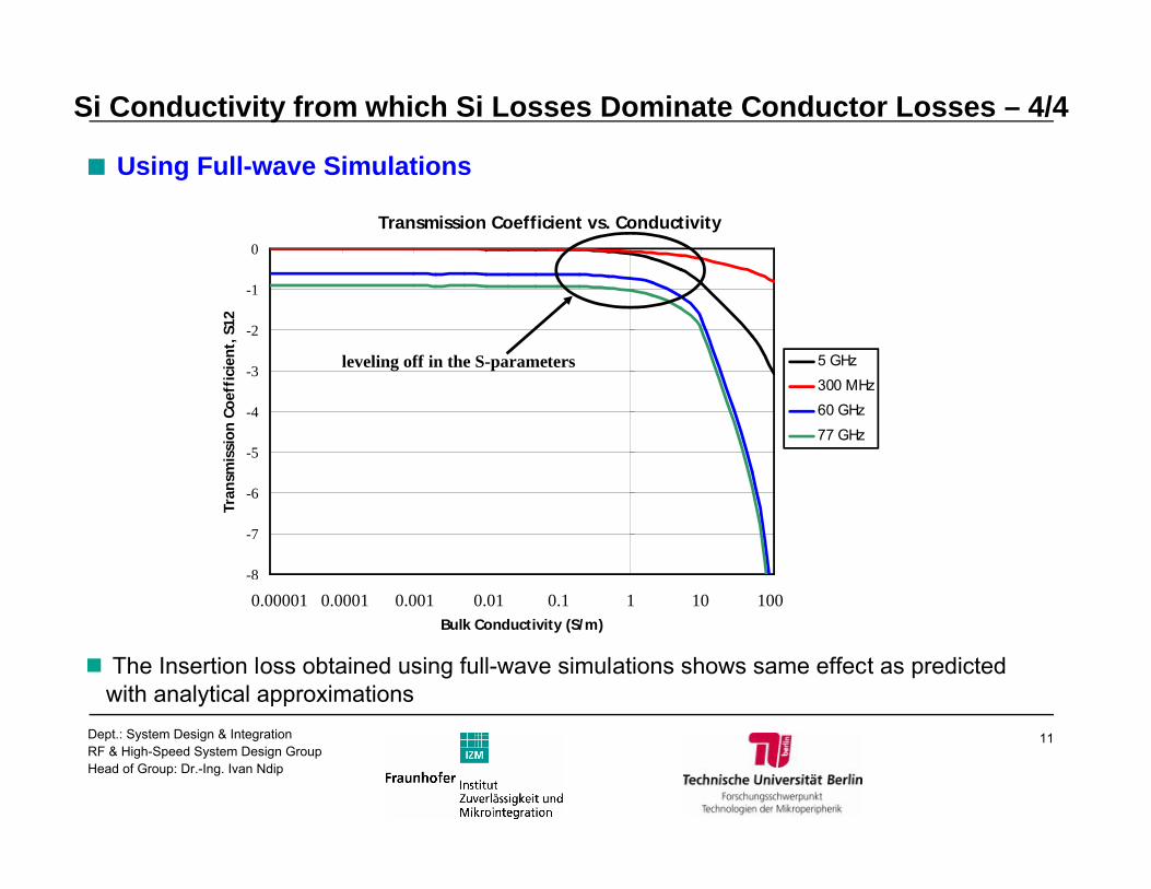
The Insertion loss obtained using full-wave simulations shows same effect as predicted with analytical approximations
Transmission Coefficient vs. Conductivity
-8
-7
-6
-5
-4
-3
-2
-1
0
-5,0 -4,0 -3,0 -2,0 -1,0 0,0 1,0 2,0
Bulk Conductivity (S/m)
Tran
smis
sio
n C
oef
fici
ent,
S12
5 GHz
300 MHz
60 GHz
77 GHz
leveling off in the S-parameters
0.00001 0.0001 0.001 0.01 0.1 1 10 100
■ Using Full-wave Simulations
Si Conductivity from which Si Losses Dominate Conductor Losses – 4/4
12Dept.: System Design & IntegrationRF & High-Speed System Design GroupHead of Group: Dr.-Ing. Ivan Ndip
Impact of Resistivity on RF Performance of TSVs – 1/2
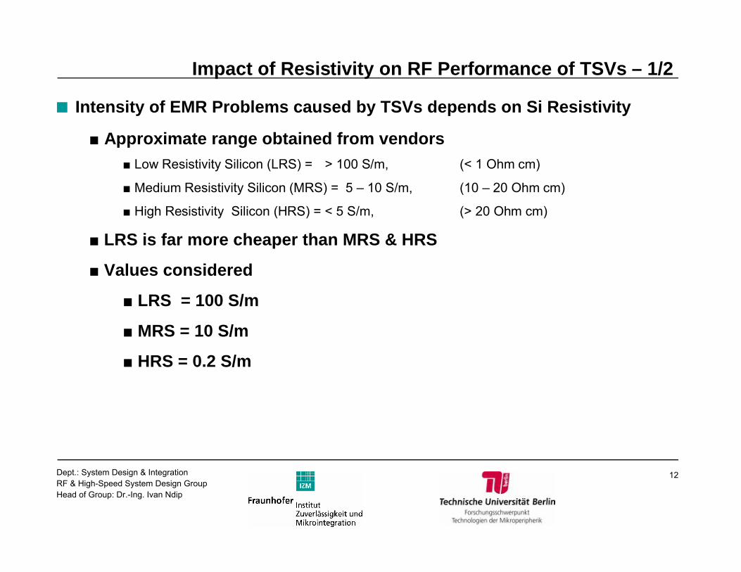
■ Intensity of EMR Problems caused by TSVs depends on Si Resistivity
■ Approximate range obtained from vendors
■ Low Resistivity Silicon (LRS) = > 100 S/m, (< 1 Ohm cm)
■ Medium Resistivity Silicon (MRS) = 5 – 10 S/m, (10 – 20 Ohm cm)
■ High Resistivity Silicon (HRS) = < 5 S/m, (> 20 Ohm cm)
■ LRS is far more cheaper than MRS & HRS
■ Values considered
■ LRS = 100 S/m
■ MRS = 10 S/m
■ HRS = 0.2 S/m
13Dept.: System Design & IntegrationRF & High-Speed System Design GroupHead of Group: Dr.-Ing. Ivan Ndip
0.00 10.00 20.00 30.00 40.00 50.00 60.00 70.00 80.00Freq [GHz]
-6.00
-5.00
-4.00
-3.00
-2.00
-1.00
0.00T
ran
smis
sio
n C
oe
ffic
ien
t, S
12
(d
B)
Ansoft Corporation HFSSDesign2XY Plot 1
0.2 S/m
10 S/m
100 S/m
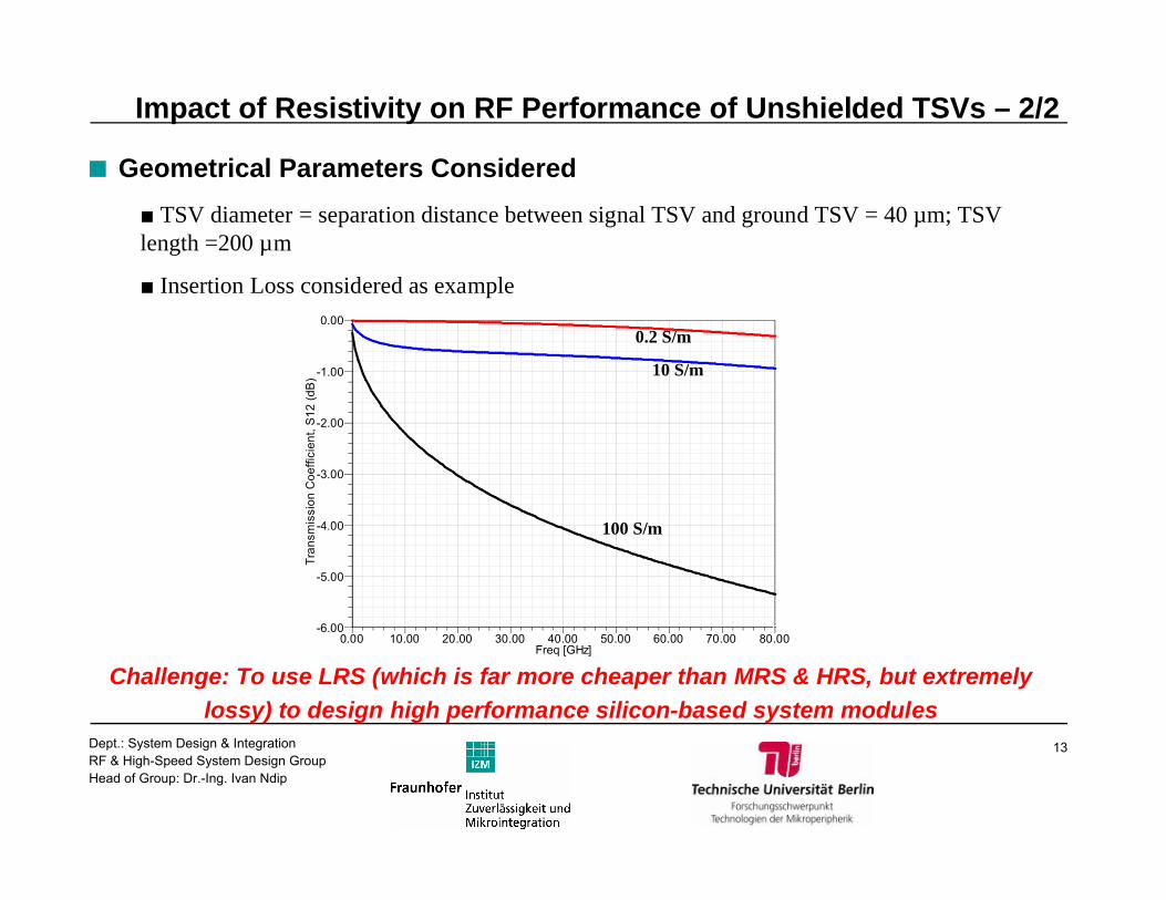
Impact of Resistivity on RF Performance of Unshielded TSVs – 2/2
■ Geometrical Parameters Considered
■ TSV diameter = separation distance between signal TSV and ground TSV = 40 µm; TSV length =200 µm
■ Insertion Loss considered as example
Challenge: To use LRS (which is far more cheaper than MRS & HRS, but extremely
lossy) to design high performance silicon-based system modules
14Dept.: System Design & IntegrationRF & High-Speed System Design GroupHead of Group: Dr.-Ing. Ivan Ndip
0.00 10.00 20.00 30.00 40.00 50.00 60.00 70.00 80.00Freq [GHz]
-40.00
-35.00
-30.00
-25.00
-20.00
-15.00
-10.00
Ne
ar
En
d C
ross
-ta
lk, S
13
(d
B)
Ansoft Corporation HFSSDesign1XY Plot 2
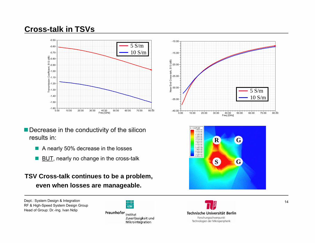
Decrease in the conductivity of the silicon results in:
A nearly 50% decrease in the losses
BUT, nearly no change in the cross-talk
0.00 10.00 20.00 30.00 40.00 50.00 60.00 70.00 80.00Freq [GHz]
-1.60
-1.50
-1.40
-1.30
-1.20
-1.10
-1.00
-0.90
-0.80
-0.70
-0.60
-0.50
Tra
nsm
issi
on
Co
effi
cie
nt,
S1
2 (
dB
)
Ansoft Corporation HFSSDesign1XY Plot 1
5 S/m10 S/m
5 S/m10 S/m
TSV Cross-talk continues to be a problem,
even when losses are manageable.
Cross-talk in TSVs
G
GS
R
15Dept.: System Design & IntegrationRF & High-Speed System Design GroupHead of Group: Dr.-Ing. Ivan Ndip
■ Motivation
■ Quantification of Some EMR Problems caused by TSVs
■ Methods for Enhancing RF Performance of TSVs in Low Resistivity Silicon
■ On-going Activities to Overcome TSV Design & Fabrication Challenges
Outline
16Dept.: System Design & IntegrationRF & High-Speed System Design GroupHead of Group: Dr.-Ing. Ivan Ndip
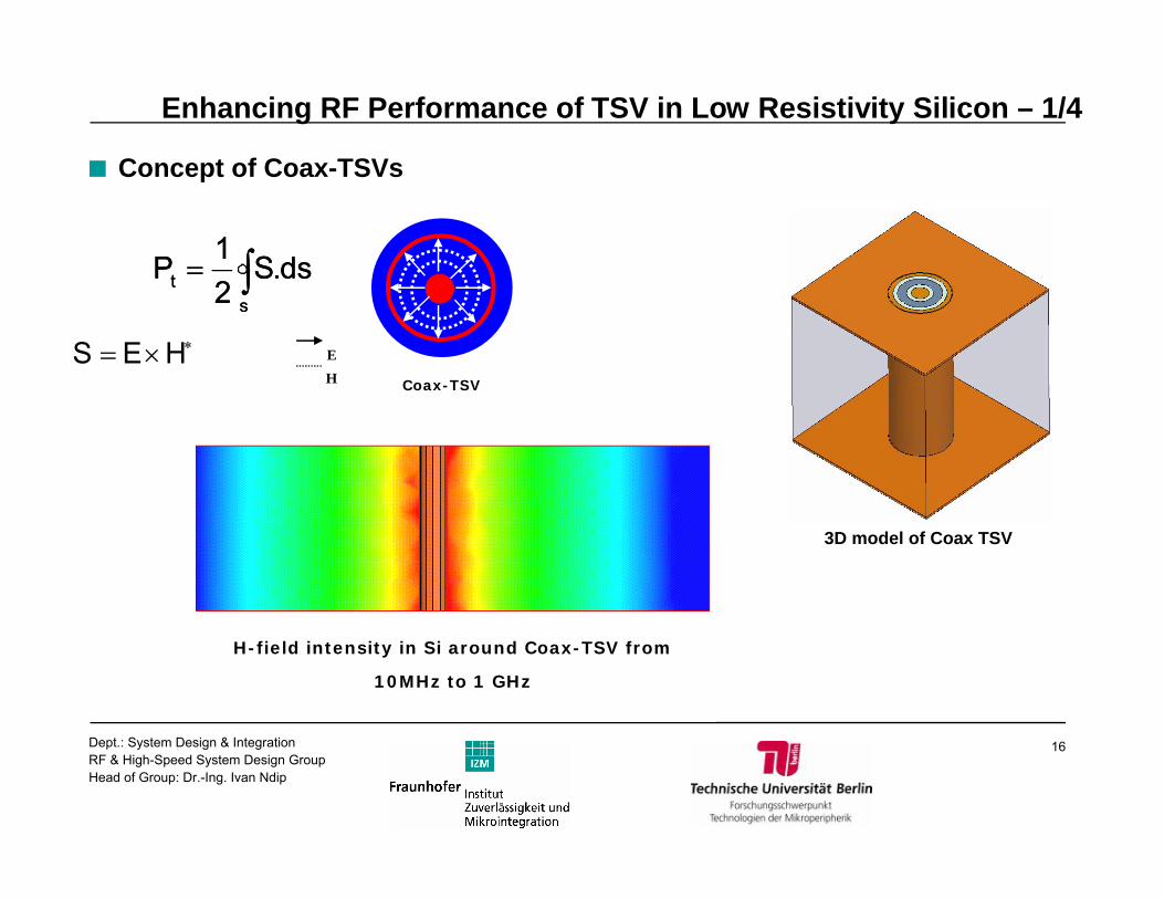
H-field intensity in Si around Coax-TSV from
10MHz to 1 GHz
Enhancing RF Performance of TSV in Low Resistivity Silicon – 1/4
■ Concept of Coax-TSVs
Coax-TSV
E
H
ts
1P S.ds
2 t
s
1P S.ds
2
S E H
3D model of Coax TSV
17Dept.: System Design & IntegrationRF & High-Speed System Design GroupHead of Group: Dr.-Ing. Ivan Ndip
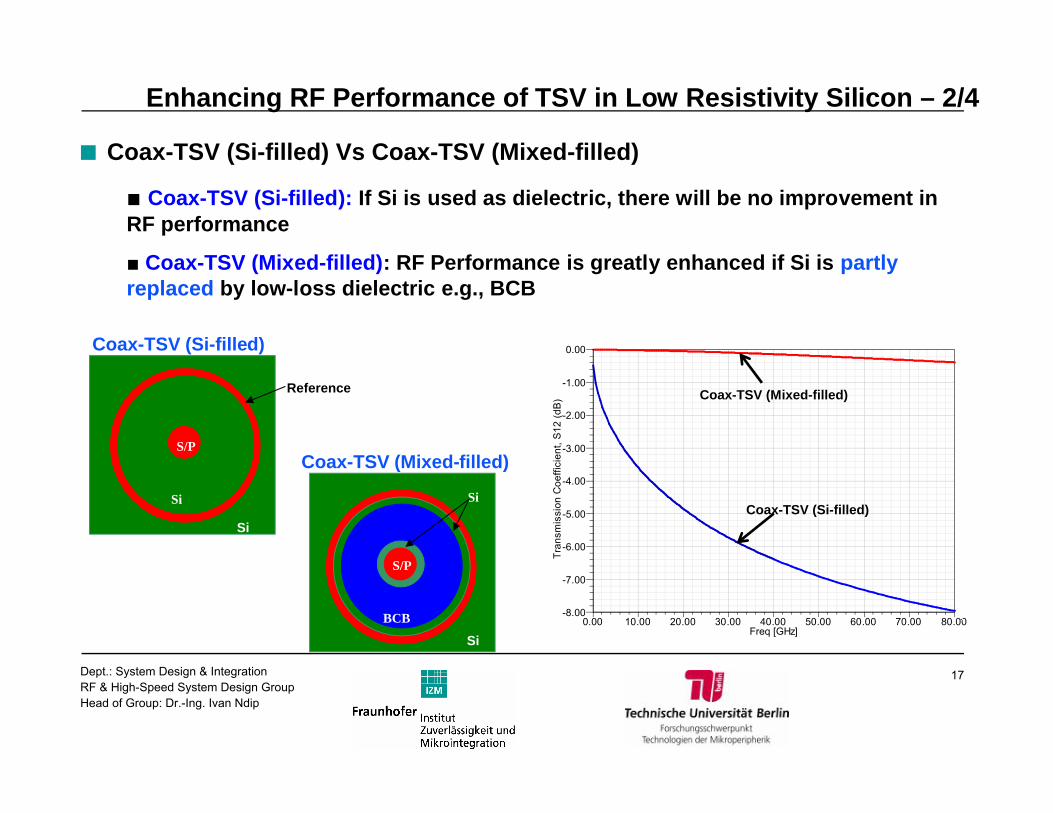
■ Coax-TSV (Si-filled) Vs Coax-TSV (Mixed-filled)
■ Coax-TSV (Si-filled): If Si is used as dielectric, there will be no improvement in RF performance
■ Coax-TSV (Mixed-filled): RF Performance is greatly enhanced if Si is partly replaced by low-loss dielectric e.g., BCB
Si
Si
Reference
S/P
0.00 10.00 20.00 30.00 40.00 50.00 60.00 70.00 80.00Freq [GHz]
-8.00
-7.00
-6.00
-5.00
-4.00
-3.00
-2.00
-1.00
0.00
Tra
nsm
issi
on
Co
eff
icie
nt,
S1
2 (
dB
)
Ansoft Corporation One_ViaXY Plot 1
BCB
Si
S/P
Si
Coax-TSV (Mixed-filled)
Coax-TSV (Si-filled)
Coax-TSV (Mixed-filled)
Coax-TSV (Si-filled)
Enhancing RF Performance of TSV in Low Resistivity Silicon – 2/4
18Dept.: System Design & IntegrationRF & High-Speed System Design GroupHead of Group: Dr.-Ing. Ivan Ndip
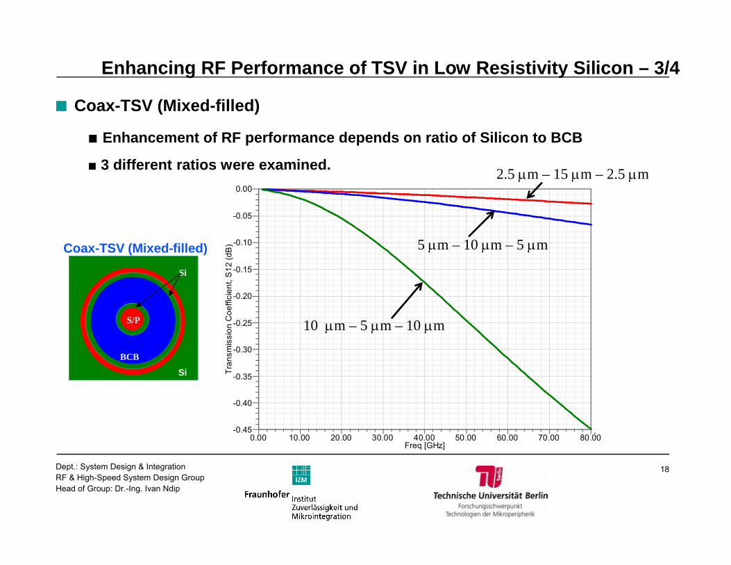
■ Coax-TSV (Mixed-filled)
■ Enhancement of RF performance depends on ratio of Silicon to BCB
■ 3 different ratios were examined.
0.00 10.00 20.00 30.00 40.00 50.00 60.00 70.00 80.00Freq [GHz]
-0.45
-0.40
-0.35
-0.30
-0.25
-0.20
-0.15
-0.10
-0.05
0.00
Tra
nsm
issi
on
Co
effi
cie
nt,
S1
2 (
dB
)
Ansoft Corporation One_ViaXY Plot 2 2.5 m – 15 m – 2.5 m
5 m – 10 m – 5 m
10 m – 5 m – 10 m
BCB
Si
S/P
Si
Coax-TSV (Mixed-filled)
Enhancing RF Performance of TSV in Low Resistivity Silicon – 3/4
19Dept.: System Design & IntegrationRF & High-Speed System Design GroupHead of Group: Dr.-Ing. Ivan Ndip
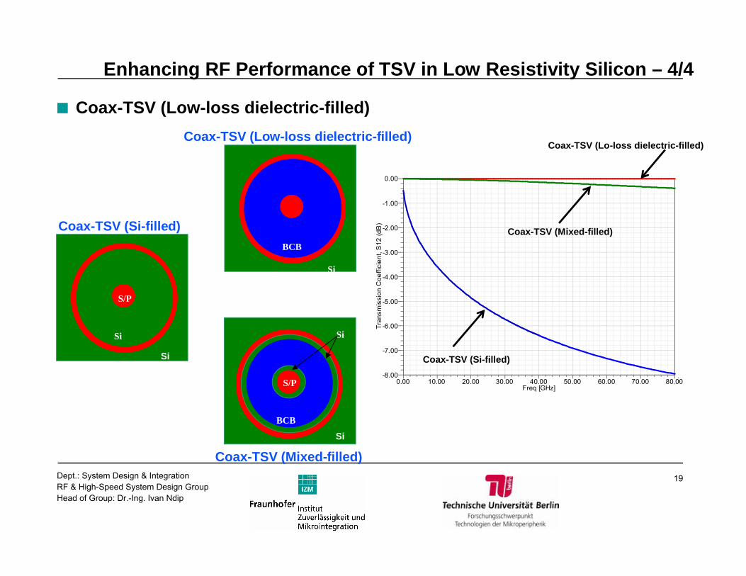
■ Coax-TSV (Low-loss dielectric-filled)
0.00 10.00 20.00 30.00 40.00 50.00 60.00 70.00 80.00Freq [GHz]
-8.00
-7.00
-6.00
-5.00
-4.00
-3.00
-2.00
-1.00
0.00
Tra
nsm
issi
on
Co
effi
cie
nt,
S1
2 (
dB
)
Ansoft Corporation One_ViaXY Plot 1
Coax-TSV (Mixed-filled)
Coax-TSV (Si-filled)
Coax-TSV (Lo-loss dielectric-filled)
BCB
Si
Si
Si
S/P
BCB
Si
S/P
Si
Coax-TSV (Mixed-filled)
Coax-TSV (Si-filled)
Coax-TSV (Low-loss dielectric-filled)
Enhancing RF Performance of TSV in Low Resistivity Silicon – 4/4
20Dept.: System Design & IntegrationRF & High-Speed System Design GroupHead of Group: Dr.-Ing. Ivan Ndip
■ Motivation
■ Quantification of Some EMR Problems caused by TSVs
■ Methods for Enhancing RF Performance of TSVs in Low Resistivity Silicon
■ On-going Activities to Overcome TSV Design & Fabrication Challenges
Outline
21Dept.: System Design & IntegrationRF & High-Speed System Design GroupHead of Group: Dr.-Ing. Ivan Ndip
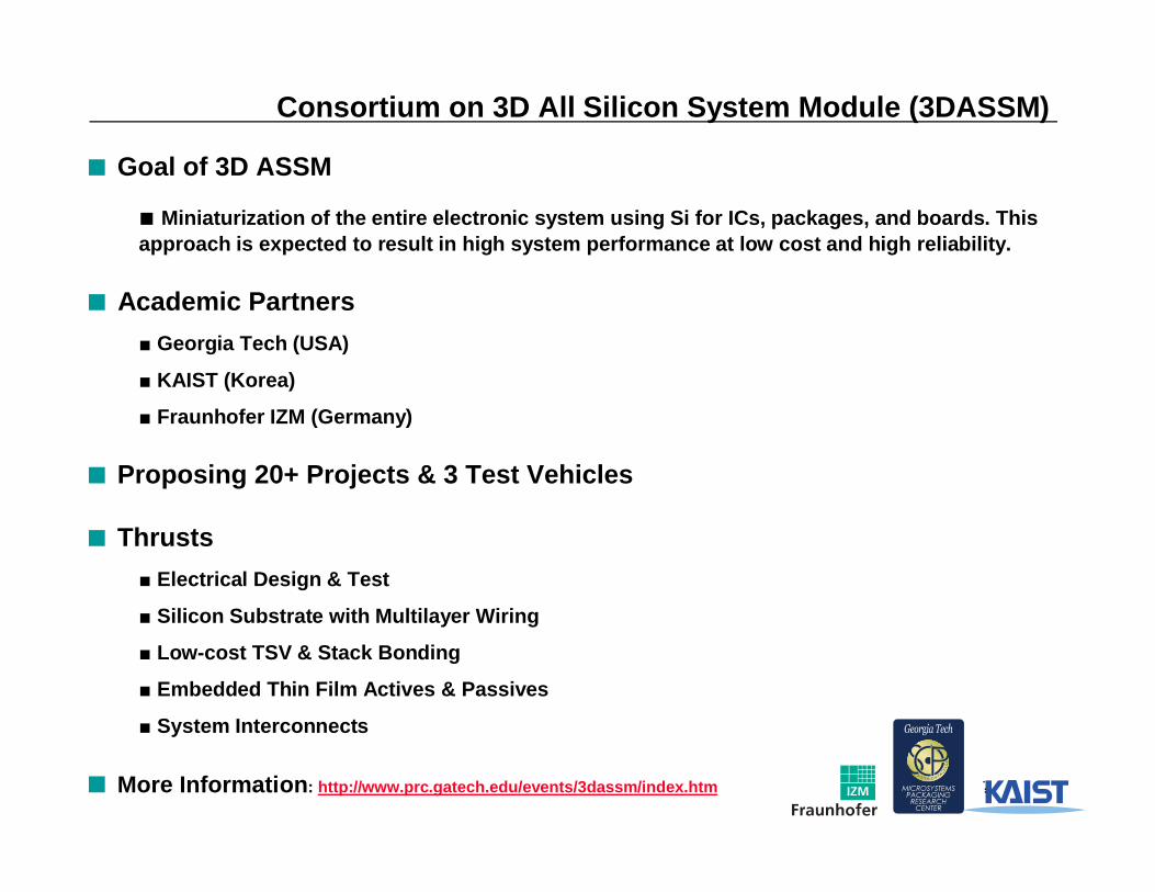
Consortium on 3D All Silicon System Module (3DASSM)
■ Goal of 3D ASSM
■ Miniaturization of the entire electronic system using Si for ICs, packages, and boards. This approach is expected to result in high system performance at low cost and high reliability.
■ Academic Partners
■ Georgia Tech (USA)
■ KAIST (Korea)
■ Fraunhofer IZM (Germany)
■ Proposing 20+ Projects & 3 Test Vehicles
■ Thrusts
■ Electrical Design & Test
■ Silicon Substrate with Multilayer Wiring
■ Low-cost TSV & Stack Bonding
■ Embedded Thin Film Actives & Passives
■ System Interconnects
■ More Information: http://www.prc.gatech.edu/events/3dassm/index.htm
22Dept.: System Design & IntegrationRF & High-Speed System Design GroupHead of Group: Dr.-Ing. Ivan Ndip
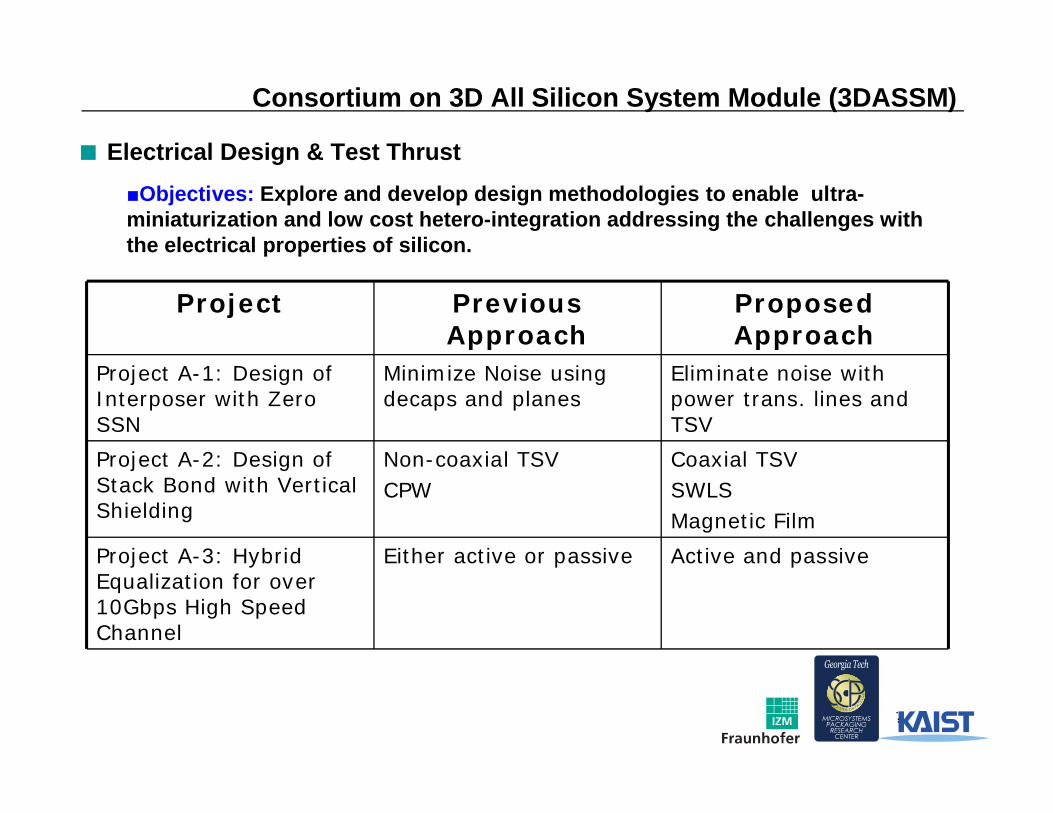
■ Electrical Design & Test Thrust
■Objectives: Explore and develop design methodologies to enable ultra-miniaturization and low cost hetero-integration addressing the challenges with the electrical properties of silicon.
Consortium on 3D All Silicon System Module (3DASSM)
Project Previous Approach
Proposed Approach
Project A-1: Design of Interposer with Zero SSN
Minimize Noise using decaps and planes
Eliminate noise with power trans. lines and TSV
Project A-2: Design of Stack Bond with Vertical Shielding
Non-coaxial TSVCPW
Coaxial TSVSWLSMagnetic Film
Project A-3: Hybrid Equalization for over 10Gbps High Speed Channel
Either active or passive Active and passive
23Dept.: System Design & IntegrationRF & High-Speed System Design GroupHead of Group: Dr.-Ing. Ivan Ndip
Thank you very much
for your attention!