Embed Size (px)
Citation preview
DESIGN AND IMPLEMENTATION OF NOVEL HIGH PERFORMANCE DOMINO LOGIC
A thesis submitted in partial fulfillment of the requirements for the award of the degree of
Doctor of Philosophy
in
VLSI Design and Embedded Systems
by
SRINIVASA V S SARMA D
Roll No: 510EC102
Under the Guidance of
Prof. KAMALAKANTA MAHAPATRA
Electronics and Communication Engineering Department
National Institute of Technology
Rourkela-769008
Odisha
2015
CERTIFICATE
This is to certify that the thesis report entitled “DESIGN AND
IMPLEMENTATION OF NOVEL HIGH PERFORMANCE DOMINO
LOGIC” submitted by Srinivasa V S Sarma D, Roll No: 510EC102, in
partial fulfillment of the requirements for the award of the degree of Doctor of
Philosophy with specialization in “VLSI Design and Embedded Systems”
in Electronics and Communication Engineering at the National Institute
of Technology, Rourkela is an authentic work under my supervision and
guidance.
To the best of my knowledge, the matter embodied in the thesis has not been
submitted to any other University / Institute for the award of any Degree or
Diploma.
Place: NIT ROURKELA
Date: Prof. K. K. Mahapatra Electronics & Communication Engineering Department,
National Institute of Technology,
Rourkela - 769008.

Dedicated to
My parents

i
ACKNOWLEDGEMENTS
This project is by far the most significant accomplishment in my life and it would be
impossible without people (especially my family) who supported me and believed in me.
I express my deep sense of gratitude to Dr. K. K. Mahapatra, Professor in the
Department of Electronics and Communication Engineering, NIT Rourkela for giving me
the opportunity to work under him and lending every support at every stage of this research
work. I am indebted to his esteemed guidance, constant encouragement and fruitful
suggestions from the beginning to the end of this thesis. His trust and support inspired me
in the most important moments of making right decisions and I am really blessed to be
student of him without whom this work would not have been possible.
I am thankful to all my teachers Prof. S.K. Patra, Prof. S. Meher, Prof.
D.P.Acharya, Prof.A.K.Swain and all other faculty members for providing a solid
background for my studies and research thereafter.
My sincere and heart full thanks to Dr. S. K. Sarangi, Director of NIT-Rourkela,
for providing the working platform and required research equipment in the department
laboratory at NIT.
Also, I would like to thank all my classmates and friends (Bhaskar, Govind, Vijay,
Preethi, Ramakrishna, Rajesh Patjoshi, Gokulanand and others) of VLSI lab who always
encouraged me in the successful completion of my thesis work. I am indebted to the
service provided by Ayas sir, sudi, Tom, Sauvagya, Venkat Ratnam and Jagannath who
helped me in crucial stage of submission of my thesis.
Finally, I thank GOD-Almighty for being with me forever end ever.
SRINIVASA V S SARMA D
Roll No: 510EC102
ii
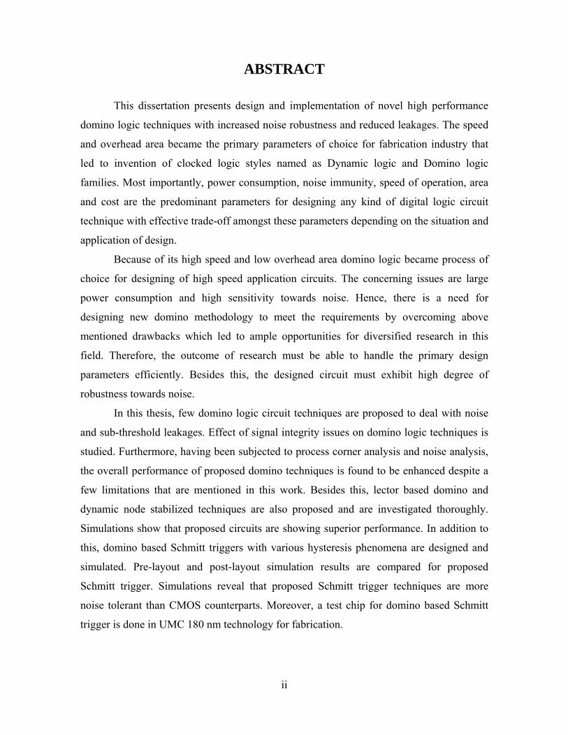
ABSTRACT
This dissertation presents design and implementation of novel high performance
domino logic techniques with increased noise robustness and reduced leakages. The speed
and overhead area became the primary parameters of choice for fabrication industry that
led to invention of clocked logic styles named as Dynamic logic and Domino logic
families. Most importantly, power consumption, noise immunity, speed of operation, area
and cost are the predominant parameters for designing any kind of digital logic circuit
technique with effective trade-off amongst these parameters depending on the situation and
application of design.
Because of its high speed and low overhead area domino logic became process of
choice for designing of high speed application circuits. The concerning issues are large
power consumption and high sensitivity towards noise. Hence, there is a need for
designing new domino methodology to meet the requirements by overcoming above
mentioned drawbacks which led to ample opportunities for diversified research in this
field. Therefore, the outcome of research must be able to handle the primary design
parameters efficiently. Besides this, the designed circuit must exhibit high degree of
robustness towards noise.
In this thesis, few domino logic circuit techniques are proposed to deal with noise
and sub-threshold leakages. Effect of signal integrity issues on domino logic techniques is
studied. Furthermore, having been subjected to process corner analysis and noise analysis,
the overall performance of proposed domino techniques is found to be enhanced despite a
few limitations that are mentioned in this work. Besides this, lector based domino and
dynamic node stabilized techniques are also proposed and are investigated thoroughly.
Simulations show that proposed circuits are showing superior performance. In addition to
this, domino based Schmitt triggers with various hysteresis phenomena are designed and
simulated. Pre-layout and post-layout simulation results are compared for proposed
Schmitt trigger. Simulations reveal that proposed Schmitt trigger techniques are more
noise tolerant than CMOS counterparts. Moreover, a test chip for domino based Schmitt
trigger is done in UMC 180 nm technology for fabrication.

iii
Contents ACKNOWLEDGEMENTS ................................................................................................... i
ABSTRACT .......................................................................................................................... ii
LIST OF FIGURES ............................................................................................................. vi
LIST OF TABLES ................................................................................................................. x
ABBREVIATIONS ............................................................................................................ xii
CHAPTER 1 .......................................................................................................................... 1
INTRODUCTION ................................................................................................................. 1
1.1 Introduction ............................................................................................................. 1
1.2 History ..................................................................................................................... 2
1.3 Motivation ............................................................................................................... 3
1.4 Objectives of the research work .............................................................................. 3
1.5 Thesis structure and over all contribution ............................................................... 3
1.6 Conclusion ............................................................................................................... 5
CHAPTER 2 .......................................................................................................................... 6
OVERVIEW OF LOGIC STYLES AND RELATED WORK ............................................. 6
2.1 CMOS AND NMOS ............................................................................................... 6
2.2 Different static logic styles .................................................................................... 12
2.2.1 Pseudo N-MOS .............................................................................................. 12
2.2.2 Differential Cascode Voltage Swing Logic (DCVSL) .................................. 13
2.2.3 Pass Transistor Logic ..................................................................................... 14
2.2.4 Differential / Complementary Pass Transistor Logic .................................... 15
2.3 Dynamic CMOS logic design ................................................................................ 17
2.4 Domino logic circuits ............................................................................................ 19
2.4.1 Impact on power consumption ....................................................................... 23
2.4.2 Technique to compensate charge lost, through PMOS keeper ...................... 26
2.5 Conclusion ............................................................................................................. 31
CHAPTER 3 ........................................................................................................................ 32
NOVEL DOMINO LOGIC TOPOLOGIES ........................................................................ 32
3.1 Introduction ........................................................................................................... 32
3.2 Different high-performance noise tolerant circuit techniques ............................... 34
3.2.1 Wide fan-in Domino OR gate-Footless and Footed schemes ........................ 34

iv
3.2.2 Wide fan-in Domino OR gate Diode footed scheme ..................................... 37
3.2.3 Wide fan-in Domino OR gate-Replicated evaluation scheme ....................... 40
3.2.4 Wide fan-in Domino OR gate-Dynamic node footed scheme ....................... 41
3.2.5 Wide fan-in Domino OR gate-Clock delayed single keeper scheme ............. 44
3.2.6 Wide fan-in Domino OR gate-Clock delayed dual keeper scheme ............... 45
3.2.7 Wide fan-in Domino OR gate-Skew tolerant high speed scheme ................. 47
3.2.8 Wide fan-in Domino OR gate-Source following evaluation gate (SFEG) scheme 49
3.3 UNG & ANTE ....................................................................................................... 50
3.4 Process Corner analysis ......................................................................................... 53
3.5 Novel high-performance noise tolerant domino logic circuit techniques ............. 55
3.5.1 Wide fan-in domino OR gate with proposed technique-1 ............................. 55
3.5.2 Wide fan-in domino OR gate with proposed technique-2 ............................. 60
3.5.3 Wide fan-in domino OR gate with proposed technique-3 ............................. 65
3.6 Simulation results and discussion .......................................................................... 71
3.7 Conclusion ............................................................................................................. 80
CHAPTER 4 ........................................................................................................................ 82
SIGNAL INTEGRITY ISSUES & MODIFIED CIRCUIT TECHNIQUES ....................... 82
4.1 Introduction ........................................................................................................... 82
4.2 Signal integrity issues in clocked logic circuits .................................................... 84
4.3 Related work on lector power reduction technique ............................................... 97
4.4 Proposed Domino lector technique and dynamic node stabilizing technique ..... 101
4.5 Simulation results and discussion ........................................................................ 114
4.6 Conclusion ........................................................................................................... 122
CHAPTER 5 ...................................................................................................................... 125
DESIGN OF VARIOUS DOMINO BASED SCHMITT TRIGGER CIRCUITS ............ 125
5.1 Introduction ......................................................................................................... 125
5.2 Conventional Schmitt triggers ............................................................................. 126
5.2.1 Op-amp based Schmitt trigger ..................................................................... 126
5.2.2 CMOS Schmitt trigger ................................................................................. 131
5.3 Proposed domino Schmitt trigger ........................................................................ 142
5.3.1 Proposed domino Schmitt trigger-1 ............................................................. 142

v
5.3.2 Proposed domino Schmitt trigger-2 ............................................................. 147
5.4 Results and discussion ......................................................................................... 152
5.5 Conclusion ........................................................................................................... 155
CHAPTER 6 ...................................................................................................................... 156
CHIP TAPE-OUT .............................................................................................................. 156
6.1 Introduction ......................................................................................................... 156
6.2 VLSI design flow ................................................................................................ 157
6.2.1 Bottom-up (Back-end design) approach ...................................................... 158
6.2.2 Top-down (Front-end design) approach ...................................................... 160
6.2.3 Top-level approach ...................................................................................... 160
6.3 Test chip of proposed domino Schmitt trigger circuit-1 ..................................... 161
6.4 Results and discussion ......................................................................................... 169
6.5 Conclusion ........................................................................................................... 170
CHAPTER 7 ...................................................................................................................... 171
CONCLUSIONS & FUTURE WORK .............................................................................. 171
7.1 Conclusions ......................................................................................................... 171
7.2 Future work ......................................................................................................... 173
Bibliography ....................................................................................................................... 174

vi
LIST OF FIGURES Fig. 1.1 Moore’s law .............................................................................................................. 2 Fig. 2.1 Static CMOS logic Inverter ...................................................................................... 6 Fig. 2.2 Static CMOS 2-input NAND gate ............................................................................ 7 Fig. 2.3 Static CMOS 2-input NAND gate simulation .......................................................... 8 Fig. 2.4 NMOS 2-input NAND gate .................................................................................... 11 Fig. 2.5 NMOS 2-input NAND gate simulation .................................................................. 11 Fig. 2.6 Pseudo N-MOS Logic ............................................................................................. 12 Fig. 2. 7 Differential Cascode Voltage Swing Logic ........................................................... 13 Fig. 2.8 Pass Transistor Logic implementation of 2-input AND gate ................................. 14 Fig. 2.9 Differential/Complementary Pass Transistor Logic implementation of 2-input AND gate ............................................................................................................................. 15 Fig. 2.10 Transmission Gate ................................................................................................ 16 Fig. 2.11 2:1 Multiplexer using Transmission Gate ............................................................. 16 Fig. 2.12 Dynamic CMOS logic .......................................................................................... 17 Fig. 2.13 Block diagram of Domino logic ........................................................................... 19 Fig. 2.14 Domino CMOS logic ............................................................................................ 20 Fig. 2.15 Domino CMOS 2-input AND gate ....................................................................... 20 Fig. 2.16 Domino CMOS 2-input AND gate simulation ..................................................... 21 Fig. 2.17 Domino CMOS 2-input AND gate ....................................................................... 24 Fig. 2.18 Domino CMOS 2-input AND gate simulation ..................................................... 25 Fig. 2.19 Clock signal in Domino logic Circuit ................................................................... 26 Fig. 2.20 Domino CMOS logic circuit with weak PMOS Keeper ....................................... 27 Fig. 2.21 Domino CMOS 2 Input AND gate with weak PMOS Keeper ............................. 29 Fig. 2.22 A Domino CMOS 2 Input AND gate with weak PMOS Keeper simulation ....... 29 Fig. 3.1 Wide fan-in domino OR gate-footless .................................................................... 34 Fig. 3.2 Wide fan-in domino OR gate-footed ...................................................................... 34 Fig. 3.3 Domino 2-input OR gate-footless simulation ......................................................... 36 Fig. 3.4 Domino 2-input OR gate-footed simulation ........................................................... 37 Fig. 3.5 Wide fan-in Domino OR gate-Diode footed scheme ............................................. 37 Fig. 3.6 Domino 2-input OR gate-Diode footed scheme simulation ................................... 38 Fig. 3.7 Wide fan-in Domino OR gate-Replicated evaluation scheme ................................ 40 Fig. 3.8 Domino 2-input OR gate-Replicated evaluation scheme simulation ..................... 40 Fig. 3.9 Wide fan-in Domino OR gate-Dynamic node footed scheme ................................ 41 Fig. 3.10 Domino 2-input OR gate-Dynamic node footed scheme simulation .................... 42 Fig. 3.11 Transparency Window-phase3 waveform ............................................................ 43 Fig. 3.12 Wide fan-in Domino OR gate-Clock delayed single keeper scheme ................... 44 Fig. 3.13 Domino 2-input OR gate-Clock delayed single keeper scheme simulation ......... 45 Fig. 3.14 Wide fan-in Domino OR gate-Clock delayed dual keeper scheme ...................... 45 Fig. 3.15 Domino 2-input OR gate-Clock delayed dual keeper scheme simulation ............ 46 Fig. 3.16 Wide fan-in Domino OR gate-Skew tolerant high speed scheme ........................ 47
vii
Fig. 3.17 Domino 2-input OR gate-Skew tolerant high speed scheme simulation .............. 47 Fig. 3.18 Wide fan-in Domino OR gate-Source following evaluation gate (SFEG) scheme .............................................................................................................................................. 49 Fig. 3.19 Domino 2-input OR gate -Source following evaluation gate (SFEG) scheme simulation ............................................................................................................................. 49 Fig. 3.20 Typical UNG measurement wave form ................................................................ 52 Fig. 3.21 Wide fan-in domino OR gate with proposed technique-1 .................................... 55 Fig. 3.22 Domino 2-input OR gate with proposed technique-1 simulation ......................... 56 Fig. 3.23 Pre-charge operation of proposed technique-1 ..................................................... 57 Fig. 3.24 Evaluation phase when PDN is off - operation of proposed technique-1 ............. 59 Fig. 3.25 Evaluation phase when PDN is on - operation of proposed technique-1 ............. 59 Fig. 3.26 Wide fan-in domino OR gate with proposed technique-2 .................................... 60 Fig. 3.27 Domino 2-input OR gate with proposed technique-2 simulation ......................... 61 Fig. 3.28 Pre-charge operation of proposed technique-2 ..................................................... 62 Fig. 3.29 Evaluation phase when PDN is off - operation of proposed technique-1 ............. 63 Fig. 3.30 Evaluation phase when PDN is on - operation of proposed technique-2 ............. 64 Fig. 3.31 Wide fan-in domino OR gate with proposed technique-3 .................................... 65 Fig. 3.32 Domino 2-input OR gate with proposed technique-3 simulation ......................... 65 Fig. 3.33 A Transmission logic gate circuit ......................................................................... 66 Fig. 3.34 A 2:1 Multiplexer using transmission logic gate circuit ....................................... 67 Fig. 3.35 Pre-charge operation of proposed technique-3 ..................................................... 68 Fig. 3.36 Evaluation phase when PDN is off - operation of proposed technique-3 ............. 69 Fig. 3.37 Evaluation phase when PDN is on - operation of proposed technique-3 ............. 70 Fig. 3.38 ANTE Vs Fan-in for Process corner=NN ............................................................. 75 Fig. 3.39 ANTE Vs Fan-in for Process corner=FF .............................................................. 76 Fig. 3.40 ANTE Vs Fan-in for Process corner=SS .............................................................. 76 Fig. 3.41 ANTE Vs Fan-in for Process corner=FS .............................................................. 77 Fig. 4.1 Cross talk noise effect ............................................................................................. 85 Fig. 4.2 Charge leakages in dynamic logic circuit ............................................................... 86 Fig. 4.3 Keeper with always ON configuration ................................................................... 88 Fig. 4.4 Keeper with feedback configuration ....................................................................... 88 Fig. 4.5 Charge sharing analysis with 2-input domino AND gate ....................................... 89 Fig. 4.6 Charge sharing analysis with wide fan-in (with fan-in=P) domino AND gate ...... 93 Fig. 4.7 Capacitive coupling phenomenon in domino logic circuits ................................... 94 Fig. 4.8 Clock feed-through phenomenon dynamic logic circuits ....................................... 96 Fig. 4.9 Implementation of 2-input NAND gate using (a) static CMOS (b) lector scheme 99 Fig. 4.10 DC characteristics of 2-input static CMOS NAND gate .................................... 100 Fig. 4.11 DC characteristics of 2-input lector NAND gate ................................................ 100 Fig. 4.12 Direct method of implementing lector domino logic circuit .............................. 103 Fig. 4.13 Proposed lector domino logic circuit technique ................................................. 104 Fig. 4.14 Simulation of Proposed lector 2-input domino OR gate logic circuit ................ 105
viii
Fig. 4.15 Proposed dynamic node stabilizing technique .................................................... 105 Fig. 4.16 Proposed dynamic node stabilizing technique applied to basic domino logic circuit ................................................................................................................................. 106 Fig. 4.17 Impact of PMOS stack network on power consumption .................................... 108 Fig. 4.18 Dynamic node voltage drop for 2-input dynamic NOR gate .............................. 111 Fig. 4.19 Dynamic node voltage drop for 2-input dynamic NOR gate with n=1 .............. 112 Fig. 4.20 Dynamic node voltage drop for 2-input dynamic NOR gate with n=8 .............. 112 Fig. 4.21 Variation of Power-delay-product with number (n) of PMOS stack devices for proposed dynamic and domino 2-input OR gate................................................................ 119 Fig. 5.1 Basic open-loop polarity indicator ........................................................................ 126 Fig. 5.2 Basic open-loop comparator ................................................................................. 127 Fig. 5.3 Op-amp based Schmitt trigger configuration ....................................................... 128 Fig. 5.4 Output of op-amp based Schmitt trigger with respect to various reference signal voltages When Vref = 0 V, (b) When Vref = 4 V and (c) When Vref = -4 V [5] .................. 129 Fig. 5.5 Hysteresis of op-amp based Schmitt trigger ......................................................... 130 Fig. 5.6 CMOS Schmitt trigger (ST)-1 .............................................................................. 132 Fig. 5.7 Voltage Transfer Characteristic (VTC) curve of CMOS Schmitt trigger-1 ......... 133 Fig. 5.8 Simulation of transient response of CMOS Schmitt trigger (ST)-1 ..................... 135 Fig. 5.9 Simulation of DC response (VTC) of CMOS Schmitt trigger (ST)-1 .................. 135 Fig. 5.10 Simulation of sinusoidal response of CMOS Schmitt trigger (ST)-1 ................. 136 Fig. 5.11 CMOS Schmitt trigger (ST)-2 ............................................................................ 137 Fig. 5.12 Simulation of DC response (VTC) of CMOS Schmitt trigger (ST)-2 ................ 137 Fig. 5.13 Simulation of transient response of CMOS Schmitt trigger (ST)-2 ................... 138 Fig. 5.14 Node voltages of CMOS Schmitt trigger (ST)-2 ................................................ 138 Fig. 5.15 Simulation of sinusoidal response of CMOS Schmitt trigger (ST)-2 ................. 139 Fig. 5.16 Schmitt trigger (ST)-3 Fig. 5.17 Schmitt trigger (ST)-4 ... 140 Fig. 5.18 Schmitt trigger (ST)-5 ......................................................................................... 140 Fig. 5.19 Transient and DC response of Schmitt trigger (ST)-3 ........................................ 141 Fig. 5.20 Transient and DC response of Schmitt trigger (ST)-4 ........................................ 141 Fig. 5.21 Transient and DC response of Schmitt trigger (ST)-5 ........................................ 142 Fig. 5.22 Proposed domino Schmitt trigger-1 .................................................................... 143 Fig. 5.23 Simulation of transient response of domino Schmitt trigger-1 ........................... 143 Fig. 5.24 Simulation of DC response (VTC) of domino Schmitt trigger-1 ....................... 144 Fig. 5.25 Pre-charge operation of proposed domino Schmitt trigger-1 ............................. 145 Fig. 5.26 Evaluation phase when PDN is off - operation of proposed domino Schmitt trigger-1 .............................................................................................................................. 146 Fig. 5.27 Evaluation phase when PDN is on - operation of proposed domino Schmitt trigger-1 .............................................................................................................................. 146 Fig. 5.28 Proposed domino Schmitt trigger-2 .................................................................... 148 Fig. 5.29 Simulation of transient response of domino Schmitt trigger-2 ........................... 148 Fig. 5.30 Simulation of DC response (VTC) of domino Schmitt trigger-2 ....................... 149
ix
Fig. 5.31 Pre-charge operation of proposed domino Schmitt trigger-2 ............................. 149 Fig. 5.32 Evaluation phase when PDN is off - operation of proposed domino Schmitt trigger-2 .............................................................................................................................. 150 Fig. 5.33 Evaluation phase when PDN is on - operation of proposed domino Schmitt trigger-2 .............................................................................................................................. 151 Fig. 5.34 Noise Margin levels ............................................................................................ 155 Fig. 6.1 Flow chart of basic VLSI design flow .................................................................. 157 Fig. 6.2 Schematic implementation of proposed domino Schmitt trigger-1 ...................... 161 Fig. 6.3 Transistor level simulation of proposed domino Schmitt trigger-1-transient response .............................................................................................................................. 162 Fig. 6.4 Transistor level simulation of proposed domino Schmitt trigger-1-DC response 162 Fig. 6.5 Schematic layout of proposed domino Schmitt trigger-1 ..................................... 163 Fig. 6.6 DRC report of proposed domino Schmitt trigger-1 .............................................. 163 Fig. 6.7 Parasitic extraction report of proposed domino Schmitt trigger-1 ....................... 164 Fig. 6.8 Parasitic components (resistors and capacitors) of extracted layout of proposed domino Schmitt trigger-1 ................................................................................................... 164 Fig. 6.9 Summary report after LVS check for proposed domino Schmitt trigger-1 .......... 165 Fig. 6.10 Report of LVS check for proposed domino Schmitt trigger-1 ........................... 165 Fig. 6.11 Post-layout simulation of proposed domino Schmitt trigger-1-transient response ............................................................................................................................................ 166 Fig. 6.12 Post-layout simulation of proposed domino Schmitt trigger-1-DC (VTC) response .............................................................................................................................. 166 Fig. 6.13 Final chip tape-out of proposed domino Schmitt trigger-1 circuit ..................... 167
x
LIST OF TABLES Table 2.1 Comparison of parameters with technology scaling for Domino CMOS 2-input AND gate ............................................................................................................................. 24 Table 2.2 Comparison of parameters with technology scaling for Domino CMOS 2-input AND gate with PMOS keeper .............................................................................................. 30 Table 3.1 Comparison of typical power parameters and power-delay-product for standard and proposed domino logic techniques ................................................................................ 71 Table 3.2 UNG and ANTE comparison of standard and proposed domino logic techniques with Fan-in 2 ........................................................................................................................ 72 Table 3.3 UNG comparison of proposed domino logic techniques with Fan-in=2 at different Process Corner analysis ......................................................................................... 73 Table 3.4 UNG comparison of proposed domino logic techniques with Fan-in=4 at different Process Corner analysis ......................................................................................... 73 Table 3.5 UNG comparison of proposed domino logic techniques with Fan-in=8 at different Process Corner analysis ......................................................................................... 74 Table 3.6 UNG comparison of proposed domino logic techniques with Fan-in=16 at different Process Corner analysis ......................................................................................... 74 Table 3.7 UNG comparison of proposed domino logic techniques with Fan-in=32 at different Process Corner analysis ......................................................................................... 75 Table 4.1 Condition of all transistors of lector 2–input NAND gate for all possible combinations of inputs ....................................................................................................... 101 Table 4.2 Comparison of various parameters for Static CMOS NAND and Lector NAND techniques ........................................................................................................................... 114 Table 4.3 Comparison of various parameters for domino lector-direct method and proposed domino lector technique ..................................................................................................... 114 Table 4.4 UNG and ANTE comparison of domino lector-direct method and proposed domino lector technique with Fan-in=2 ............................................................................. 114 Table 4.5 UNG comparison of proposed domino logic techniques with Fan-in=2 at different Process Corner analysis ....................................................................................... 115 Table 4.6 UNG comparison of proposed domino logic techniques with Fan-in=4 at different Process Corner analysis ....................................................................................... 115 Table 4.7 UNG comparison of proposed domino logic techniques with Fan-in=8 at different Process Corner analysis ....................................................................................... 116 Table 4.8 UNG comparison of proposed domino logic techniques with Fan-in=16 at different Process Corner analysis ....................................................................................... 116 Table 4.9 UNG comparison of proposed domino logic techniques with Fan-in=32 at different Process Corner analysis ....................................................................................... 117 Table 4.10 Comparison of power and delay parameters of proposed technique for 2-input dynamic NOR gate with variable n (number of PMOS stack devices).............................. 117 Table 4.11 Comparison of power and delay parameters of proposed technique for 2-input domino OR gate with variable n (number of PMOS stack devices) .................................. 118
xi
Table 4.12 UNG and ANTE comparison of proposed technique applied for domino 2-input OR gate for various stack devices ...................................................................................... 118 Table 5.1 Comparison of typical power parameters and power-delay-product of various CMOS and proposed domino Schmitt trigger circuits ....................................................... 153 Table 5.2 Comparison of noise margin, hysteresis voltage and undefined regions of various CMOS and proposed domino Schmitt trigger circuits ....................................................... 153 Table 6.1 Comparison of design parameters of domino Schmitt trigger-1 at CMOS 90 nm and CMOS 180 nm process technology ............................................................................. 169 Table 6.2 Comparison of design parameters of domino Schmitt trigger-1 at pre-layout and post-layout simulation stages ............................................................................................. 169

xii
ABBREVIATIONS
MOSFET Metal Oxide Semiconductor Field Effect Transistor
CMOS Complementary Metal Oxide Semiconductor
NMOS N-channel Metal Oxide Semiconductor
PMOS P-Channel Metal Oxide Semiconductor
GND Ground
VLSI Very Large Scale Integration
DCVSL Differential Cascode Voltage Swing Logic
PTL Pass Transistor Logic
DPTL Differential Pass Transistor Logic
TTL Transistor-Transistor Logic
CML Current Mode Logic
CLK Clock
PDP Power-Deley-Product
UNG Unity Noise Gain
ANTE Average Noise Threshold Energy
STHD Skew Tolerant High Speed Domino
FEL Front-End of Line
BEL Back End of Line
PUD Pull-Up Device
PDN Pull-Down Device
LCT Leakage Control Transistor
NN Normal-Normal
FF Fast-Fast
SS Slow-Slow
xiii
FS Fast-Slow
SF Slow-Fast
ST Schmitt Trigger
VTC Voltage Transfer Characteristics
NM Noise Margin
DRC Design Rule Check
LVS Layout Versus Schematic
RCX Parasitic Extraction
Op-Amp Operational Amplifier
Chapter 1 Introduction
1
CHAPTER 1 INTRODUCTION
1.1 Introduction
Complementary Metal Oxide Semiconductor for wide variety of applications in VLSI
field became the logic style of choice for the design of digital semiconductor domain
because of its low power dissipation and ease of design with increased robustness [1-6].
This became the major advantage of CMOS logic over the other available manufacturing
processes then, which suffered from flow of leakage currents or constant dissipation of
bias currents. The rapid development of VLSI technology made a remarkable shift in the
fabrication industry with its emerging qualities like high speed, low power, increased
robustness and low area overhead. Scaling brought impeccable change in the recent trends.
The evolution of various logic families like pseudo NMOS, DCVSL, PTL, and DPTL
changed the ongoing market trend in manufacturing field.
Then speed and overhead area became the primary parameters of choice for fabrication
industry that led to invention of clocked logic styles named as Dynamic logic and Domino
logic families. Power consumption, noise immunity, speed of operation, area and cost are
the predominant parameters that have to be taken into consideration before designing any
kind of digital logic circuit technique. There may be a requirement for the effective trade-
off between any two parameters depending on the situation and application of design.
Sometimes, the design techniques might not meet all the mentioned requirements in their
application, but still an optimization may be followed in order to proceed further in
research areas.
Because of its high speed and low overhead area domino logic became process of
choice for many digital circuits. The concerning issues are large power consumption and
high sensitivity towards noise. Hence, there is a need for designing new domino
methodology or improving existing techniques to meet the requirements by overcoming
the drawbacks which led to ample opportunities for diversified research in this field.
Therefore, the outcome of research must be able to handle the primary design parameters
efficiently. Besides this, the designed circuit must exhibit high degree of robustness
towards noise.
Chapter 1 Introduction
2
In this thesis, few domino logic circuit techniques are proposed to deal with noise and
sub-threshold leakages. Furthermore, few existing circuits have also been modified to
improve response. Proposed logic techniques are effective in increasing the immunity of
system towards noise and sub-threshold leakage issues. This logic is further modified using
various types of conditional keepers to design an energy-efficient circuit. Schmitt trigger,
using proposed technique, is designed and investigated for its operation. A test chip for
domino based Schmitt trigger is done in UMC 180 nm technology.
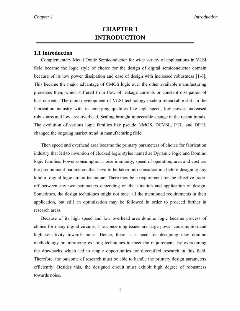
1.2 History The revolution in integration industry and IC design made an impeccable shift in VLSI
industry in the 1960s. According to Moore’s law, the number of transistors that can be
accommodated or integrated on a single die would exponentially grow with time [1].
Figure 1.1 shows Moore’s prediction. It is observed that the complexity of integration
doubles approximately every year. In the early 1970s, the microprocessor has begun to
grow up in integration complexity and high performance.
Fig. 1.1 Moore’s law

Chapter 1 Introduction
3
1.3 Motivation Besides its classical advantage of high speed operation, Domino logic family suffers
from low noise sensitivity and large power consumption [5-10]. Significant research has
been going in this field in order to stabilize this domino with reference to designing
parameters. Several techniques have been proposed to overcome the mentioned drawbacks
and most of them, however, partially improve the design parameters in various
applications.
1.4 Objectives of the research work The main aim is to design and implement domino logic circuit techniques to deal with
noise issues and enhance the primary design parameters like power, speed, leakages, noise,
area and cost. [1, 2]
The main objectives of this thesis are
(1) Study of existing domino logic circuit techniques,
(2) Simulating the benchmark circuits for analyzing the overall functionality,
(3) Improving the existing methodologies by modifying the topologies or if possible
introducing novel techniques,
(4) Making the comparison of improved circuits with existing ones and
(5) Designing of application based circuit (Schmitt Trigger) techniques based on
improved methods.
1.5 Thesis structure and over all contribution Chapter 1: Introduction
We present a generalized introduction about the broad area of research from the very basic level. In this chapter we also present the organization of the thesis and chapter wise contribution.
Chapter 2: Overview of logic styles and related work
Here the research area is primarily focused on present working environment from a
broader angle to this field. This chapter gives overview of standard logic styles in brief and
introduces the dynamic logic followed by domino logic circuits with description. The
research area is primarily focused on present working environment-Domino logic from a
broader angle. Description of various circuit styles along with their advantages and
disadvantages is illustrated with corresponding figures. In addition to this, the functioning
Chapter 1 Introduction
4
of domino logic with the encroachment of down scaling of process technology is
investigated with analysis. Technique, which uses a PMOS keeper at dynamic node, to
alleviate inevitable charge lost is reviewed and corresponding simulation result is
presented in Table 2.2. A brief review on domino logic is conducted and issues related to
domino logic are brought out that facilitated us proceeding to the next chapter.
Chapter 3: Novel Domino logic topologies
This chapter gives general introduction to domino logic family with detailed literature
survey. Standard benchmark domino logic circuit schemes followed by the analysis of their
functionality with simulation results are thoroughly investigated. In addition to this, novel
domino logic circuit techniques are proposed and are analyzed in detail with equivalent
circuit diagrams in all operating phases along with simulation results. Moreover, analysis
of benchmark circuits and proposed techniques includes variation on all the design
parameters at different ambient conditions. Furthermore, noise analysis is carried out
which includes the need for robustness, various noise metric parameters for measuring
noise immunity or robustness of domino circuits such as UNG, ANTE along with the
method of calculations, various sources of noise in domino logic circuits and their role on
operating region. Besides this, description of process corner analysis and various corners
involved in it along with their significant role on the overall functionality of the designed
domino logic circuit is presented. Also the consequences of subjecting the device to the
extreme corners with the boundary limitations are discussed. Result section shows the
calculations and comparisons of all the parameters of standard benchmark circuits and
proposed domino techniques. The primary design parameters such dynamic power, leakage
or static power, total power, PDP (power-delay-product), UNG and ANTE for wide fan-in
circuits of existing and proposed techniques are measured. The comparisons along with
graphical analysis and tabulations are made and discussed the functionality with pros and
cons.
Chapter 4: Signal integrity issues and modified circuit techniques
This chapter gives general introduction to need for power reduction and leakage
minimization. It discusses signal integrity issues in detail with simulations. A review on
prior works related to leakage power reduction schemes and the lector technique is

Chapter 1 Introduction
5
presented. Also, modified lector domino scheme and dynamic node stabilizing technique
are proposed in this chapter. All the simulations are done at CMOS 90 nm process
technology with 1 V power supply. Process corner and noise analyses are carried out for
proposed schemes. Also, the primary design parameters such dynamic power, leakage or
static power, total power, PDP (power-delay-product), UNG and ANTE for various fan-in
circuits of existing and proposed techniques are measured and comparisons are made and
conclusions are drawn in result section.
Chapter 5: Design of various domino based Schmitt trigger circuits This chapter briefly explains conventional Schmitt triggers using op-amp and CMOS
logic. Next, it demonstrates proposed domino Schmitt trigger circuits along with analysis.
A novel domino logic based noise tolerant Schmitt trigger circuit is designed and
simulated. The simulation results with discussion are presented from which concluding
remarks are made.
Chapter 6: Chip tape-out This chapter explains complete VLSI design flow which includes the process of chip
tape-out. It compares overall functionality of domino based Schmitt trigger in 180 nm and
90 nm technologies. The difference between pre-layout and post-layout simulation is
investigated. The chip tape-out of proposed domino Schmitt trigger circuit is done in
CMOS 180 nm process technology.
Chapter 7: Conclusion and future work The total work is concluded in this chapter and it also discussed future scope briefly for
further improvements based on this work.
1.6 Conclusion Therefore, the need for high speed, low power, less area and more noise tolerant
qualities is briefly discussed. As technology is growing with rapid improvements in VLSI
fields with diversified applications, there is need to achieve these target applications with
up-coming research outcomes. For that purpose, updating these present technological
library files is mandatory so as to coagulate the quality of research methodologies. This
chapter is presenting overall idea behind this work from very basic level. It briefed up the
generalized introduction, related history behind this work, motivation and main objectives
of this work. Thesis structure along with overall chapter wise contribution is also given.

Chapter 2 Overview
6
CHAPTER 2 OVERVIEW OF LOGIC STYLES AND RELATED WORK
2.1 CMOS AND NMOS FrankWanlass was the first person who in the year 1963 proposed Complementary
Metal Oxide Semiconductor which for wide variety of applications became the logic style
of choice for the design of digital semiconductor domain because of its low power
dissipation (almost no power) when the gate inputs are not altered [6]. This is implied from
the fact that CMOS structure consists of both PMOS field effect transistors which can
expeditiously drive a strong one and NMOS field effect transistors which can adequately
drive a strong zero at the output node. Therefore this peculiar combination of
complementary transistors allows CMOS logic gate circuits which are to be implemented
in such a way that the output node voltage level is always connected to either supply
voltage rail or ground rail but not both simultaneously, which there by implies that as long
as the logic inputs of CMOS circuit are not altered, there is no power dissipation by the
circuit. This became the major advantage of CMOS logic over the other available
manufacturing processes then, which suffered from flow of leakage currents or constant
dissipation of bias currents.
Fig. 2.1 Static CMOS logic Inverter
Chapter 2 Overview
7
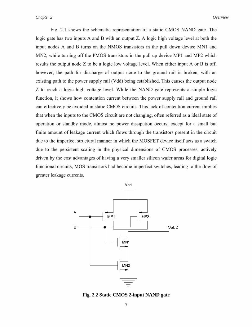
Fig. 2.1 shows the schematic representation of a static CMOS NAND gate. The
logic gate has two inputs A and B with an output Z. A logic high voltage level at both the
input nodes A and B turns on the NMOS transistors in the pull down device MN1 and
MN2, while turning off the PMOS transistors in the pull up device MP1 and MP2 which
results the output node Z to be a logic low voltage level. When either input A or B is off,
however, the path for discharge of output node to the ground rail is broken, with an
existing path to the power supply rail (Vdd) being established. This causes the output node
Z to reach a logic high voltage level. While the NAND gate represents a simple logic
function, it shows how contention current between the power supply rail and ground rail
can effectively be avoided in static CMOS circuits. This lack of contention current implies
that when the inputs to the CMOS circuit are not changing, often referred as a ideal state of
operation or standby mode, almost no power dissipation occurs, except for a small but
finite amount of leakage current which flows through the transistors present in the circuit
due to the imperfect structural manner in which the MOSFET device itself acts as a switch
due to the persistent scaling in the physical dimensions of CMOS processes, actively
driven by the cost advantages of having a very smaller silicon wafer areas for digital logic
functional circuits, MOS transistors had become imperfect switches, leading to the flow of
greater leakage currents.
Fig. 2.2 Static CMOS 2-input NAND gate
Chapter 2 Overview
8
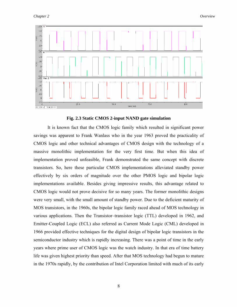
Fig. 2.3 Static CMOS 2-input NAND gate simulation
It is known fact that the CMOS logic family which resulted in significant power
savings was apparent to Frank Wanlass who in the year 1963 proved the practicality of
CMOS logic and other technical advantages of CMOS design with the technology of a
massive monolithic implementation for the very first time. But when this idea of
implementation proved unfeasible, Frank demonstrated the same concept with discrete
transistors. So, here these particular CMOS implementations alleviated standby power
effectively by six orders of magnitude over the other PMOS logic and bipolar logic
implementations available. Besides giving impressive results, this advantage related to
CMOS logic would not prove decisive for so many years. The former monolithic designs
were very small, with the small amount of standby power. Due to the deficient maturity of
MOS transistors, in the 1960s, the bipolar logic family raced ahead of MOS technology in
various applications. Then the Transistor–transistor logic (TTL) developed in 1962, and
Emitter-Coupled Logic (ECL) also referred as Current Mode Logic (CML) developed in
1966 provided effective techniques for the digital design of bipolar logic transistors in the
semiconductor industry which is rapidly increasing. There was a point of time in the early
years where prime user of CMOS logic was the watch industry. In that era of time battery
life was given highest priority than speed. After that MOS technology had begun to mature
in the 1970s rapidly, by the contribution of Intel Corporation limited with much of its early
Chapter 2 Overview
9
and advanced industrial development. Then the first and foremost world’s microprocessor
4004 was released by Intel.
The Intel microprocessor 4004 was invented with a 10 μm line width of PMOS
transistor and it used around 2300-2400 transistors running at the chip speed of 108 kHz
[8]. Again after having contributed a great research in this field Intel released an 8-bit 8080
microprocessor in the year 1974 which was manufactured with a 6 μm line width of
NMOS transistor and used 6000 transistors at the chip speed of 2MHz. Due to the higher
mobility of electrons over holes NMOS logic became faster than PMOS logic and hence
NMOS obviously started to become the choice of selection.
Advantages of CMOS Logic:
(1) Robustness(less sensitive to noise).
(2) Simple approach for implementing logic gates.
(3) Easy to translate logic to FETs.
(4) Good noise margins since FETs are in cut off & sizing not critical
(5) No static power dissipation.
(6) Low power consumption.
Disadvantages of CMOS Logic:
(1) Complexity of circuits increases with increased Fan-in.
(2) For a M-input logic gate, 2M-transistors are required which resulted in relatively large
implementation area.
(3) Propagation delay of CMOS logic gates deteriorates rapidly as a function of the Fan-in.
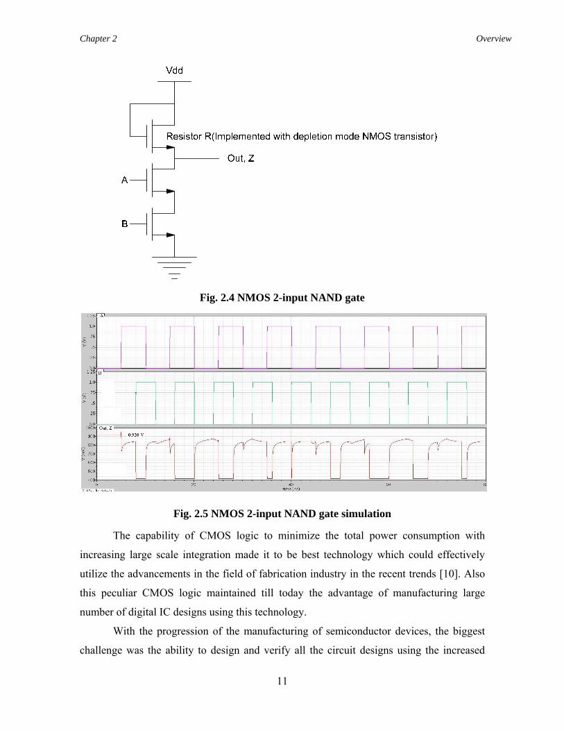
Fig. 2.4 gives the schematic implementation of a 2 input NAND gate only with NMOS
transistors. The PMOS transistors shown in Fig.2.2, MP1 and MP2 are now removed in
this implementation of logic and replaced by a resistor, R as shown. In fact the conceptual
resistor is implemented by a NMOS transistor with depletion mode. Now when either input
A or B is low, the output Z is at Vdd. When both the inputs A and B are at logic high state
then the output Z is completely discharged which resulted in logic low value. If one wants
this logic to function properly then there is a condition to be satisfied which is related to
the current-driving capability of NMOS transistors present in the pull down network which
needs to be much greater than the current-driving capability of the resistor in the pull up
network. Now this concept demonstrated that the output can be driven to a logic low
Chapter 2 Overview
10
voltage level but at the cost of higher power dissipation due to inclusion of the resistor in
the pull up network. Besides this standby power dissipation, NMOS logic is a bit slower
than CMOS logic due to the presence of weak pull up resistor that functions very slowly
when a low to high transition takes place. However the observed drawbacks might have
made the NMOS logic appear to be unappealing, still NMOS logic designs are much more
compact than CMOS logic circuits. The implementation in Fig. 2.4 has only two NMOS
transistors and a resistor R, in comparison with CMOS logic design which has four
transistors required to implement its logic. In this way the NMOS logic uses fewer
transistors and it is simpler process than CMOS logic design. Then the need to move to
CMOS technology had therefore arisen only when the advanced level of integration on
integrated circuits (ICs) made the huge standby power dissipation on the NMOS logic
circuit design unacceptable. When the 8086/8088 family of microprocessors was released
in market in the year 1978 by Intel Corporation Limited, this period of transition occurred
since all those implemented designs were almost identical to the family of 8088
microprocessors with an 8-bit bus while the family of 8086 microprocessors with a 16-bit
bus only. The power dissipation of 8086 family of microprocessors was 1.5 W with 29,000
transistors at the clock rate of 5-10 MHz, which crossed the nominal 1 W per chip power
limit for processing of plastic packaging. The increments in integration levels meant that a
32-bit microprocessor would nominally dissipate 5-6 W, leading to few severe reliability
obstacles. Only 250 mW was the power consumption of the CMOS version of the 8086
and 80C86 [9].
Chapter 2 Overview
11
Fig. 2.4 NMOS 2-input NAND gate
Fig. 2.5 NMOS 2-input NAND gate simulation
The capability of CMOS logic to minimize the total power consumption with
increasing large scale integration made it to be best technology which could effectively
utilize the advancements in the field of fabrication industry in the recent trends [10]. Also
this peculiar CMOS logic maintained till today the advantage of manufacturing large
number of digital IC designs using this technology.
With the progression of the manufacturing of semiconductor devices, the biggest
challenge was the ability to design and verify all the circuit designs using the increased
Chapter 2 Overview
12
number of transistors available then. This demand was achieved by Electronic Design
Automation (EDA) software which was developed in the hardware industry in early years.
In early days of industry, there might have been an assumption that all the existing
techniques for the implementation of digital CMOS logic would be replaced by the ASIC
design and its methodologies. That has not happened since many digital IC designs have
got their own specific needs that cannot be achieved by standard ASIC techniques. There is
a rapid and notable advancement regarding the capabilities of ASIC technology tools in the
recent years.
The important common benefits of custom IC design [13-20]:
(1) The ability to optimize across distinctly separate levels of abstractions in the ASIC
design methodologies available which leads to the development of standard cell library
used by ASIC design through sequential approach and the opportunity which is
provided by custom IC design for using logic families other than standard static logic.
(2) Also it can utilize certain type of logic families, specifically dynamic logic families
(also referred as clocked logic families), which automated the specific design
frameworks.
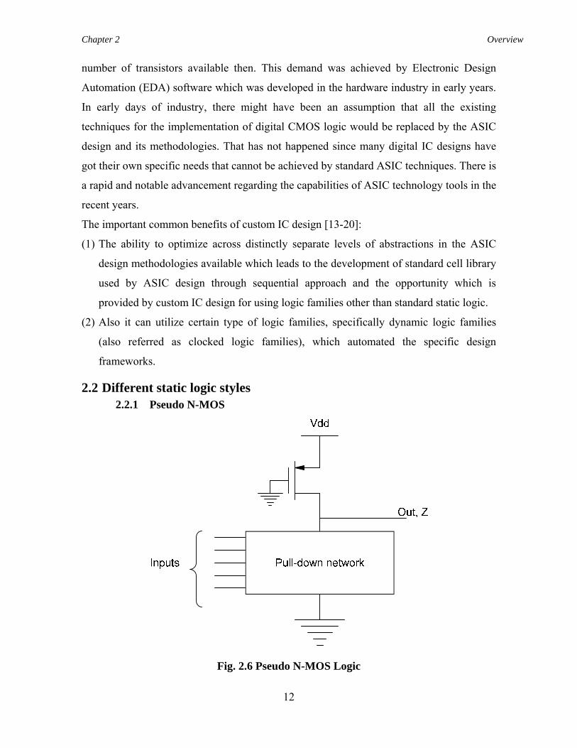
2.2 Different static logic styles 2.2.1 Pseudo N-MOS
Fig. 2.6 Pseudo N-MOS Logic
Chapter 2 Overview
13
Advantages:
For N-input logic gate implementation, only (N+1) transistors are needed. This count is
less when compared with Static CMOS Logic.
Disadvantages:
(1) Noise Margin reduces.
(2) Static power dissipation increases.
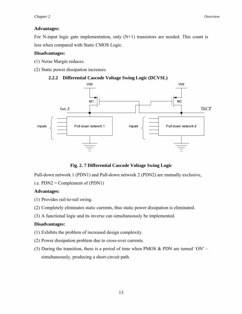
2.2.2 Differential Cascode Voltage Swing Logic (DCVSL)
Fig. 2. 7 Differential Cascode Voltage Swing Logic
Pull-down network 1 (PDN1) and Pull-down network 2 (PDN2) are mutually exclusive,
i.e. PDN2 = Complement of (PDN1)
Advantages:
(1) Provides rail-to-rail swing.
(2) Completely eliminates static currents, thus static power dissipation is eliminated.
(3) A functional logic and its inverse can simultaneously be implemented.
Disadvantages:
(1) Exhibits the problem of increased design complexity.
(2) Power dissipation problem due to cross-over currents.
(3) During the transition, there is a period of time when PMOS & PDN are turned ‘ON’ –
simultaneously, producing a short-circuit path.
Chapter 2 Overview
14
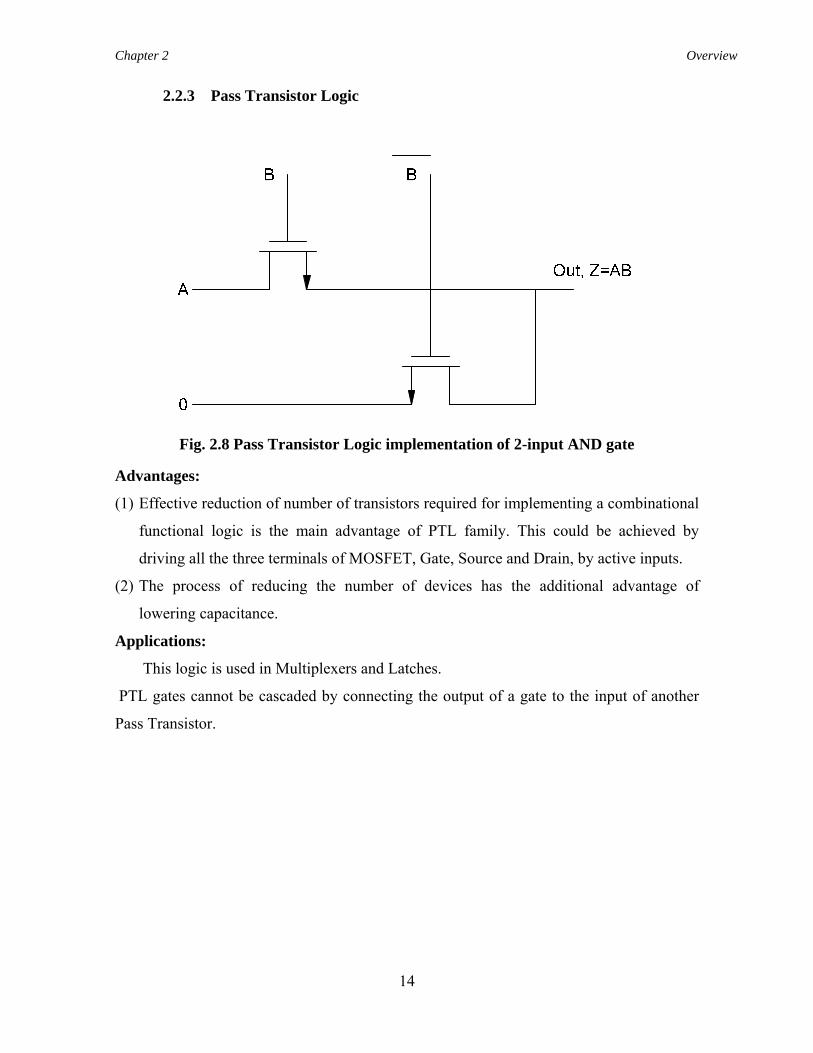
2.2.3 Pass Transistor Logic
Fig. 2.8 Pass Transistor Logic implementation of 2-input AND gate
Advantages:
(1) Effective reduction of number of transistors required for implementing a combinational
functional logic is the main advantage of PTL family. This could be achieved by
driving all the three terminals of MOSFET, Gate, Source and Drain, by active inputs.
(2) The process of reducing the number of devices has the additional advantage of
lowering capacitance.
Applications:
This logic is used in Multiplexers and Latches.
PTL gates cannot be cascaded by connecting the output of a gate to the input of another
Pass Transistor.
Chapter 2 Overview
15
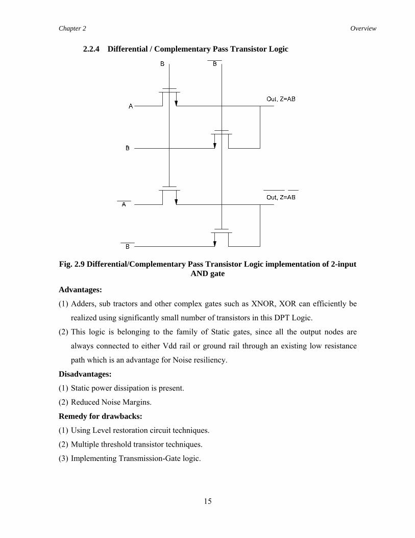
2.2.4 Differential / Complementary Pass Transistor Logic
Fig. 2.9 Differential/Complementary Pass Transistor Logic implementation of 2-input
AND gate
Advantages:
(1) Adders, sub tractors and other complex gates such as XNOR, XOR can efficiently be
realized using significantly small number of transistors in this DPT Logic.
(2) This logic is belonging to the family of Static gates, since all the output nodes are
always connected to either Vdd rail or ground rail through an existing low resistance
path which is an advantage for Noise resiliency.
Disadvantages:
(1) Static power dissipation is present.
(2) Reduced Noise Margins.
Remedy for drawbacks:
(1) Using Level restoration circuit techniques.
(2) Multiple threshold transistor techniques.
(3) Implementing Transmission-Gate logic.
Chapter 2 Overview
16
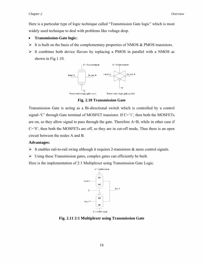
Here is a particular type of logic technique called “Transmission Gate logic” which is most
widely used technique to deal with problems like voltage drop.
• Transmission-Gate logic:
It is built on the basis of the complementary properties of NMOS & PMOS transistors.
It combines both device flavors by replacing a PMOS in parallel with a NMOS as
shown in Fig.1.10.
Fig. 2.10 Transmission Gate
Transmission Gate is acting as a Bi-directional switch which is controlled by a control
signal-‘C’ through Gate terminal of MOSFET transistor. If C=’1’, then both the MOSFETs
are on, so they allow signal to pass through the gate. Therefore A=B, while in other case if
C=’0’, then both the MOSFETs are off, so they are in cut-off mode, Thus there is an open
circuit between the nodes A and B.
Advantages:
It enables rail-to-rail swing although it requires 2-transistors & more control signals.
Using these Transmission gates, complex gates can efficiently be built.
Here is the implementation of 2:1 Multiplexer using Transmission Gate Logic.
Fig. 2.11 2:1 Multiplexer using Transmission Gate
Chapter 2 Overview
17
• When C=’0’, then transistors M1 and M2 will be ON, and there by output Z is
taking signal A.
• When C=’1’, then transistors M3 and M4 will be ON, thus they are passing signal
B to the output node Z.
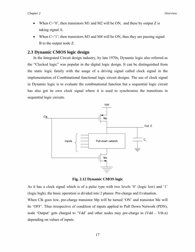
2.3 Dynamic CMOS logic design In the Integrated Circuit design industry, by late 1970s, Dynamic logic also referred as
the “Clocked logic” was popular in the digital logic design. It can be distinguished from
the static logic family with the usage of a driving signal called clock signal in the
implementation of Combinational functional logic circuit designs. The use of clock signal
in Dynamic logic is to evaluate the combinational function but a sequential logic circuit
has also got its own clock signal where it is used to synchronize the transitions in
sequential logic circuits.
Fig. 2.12 Dynamic CMOS logic
As it has a clock signal which is of a pulse type with two levels ‘0’ (logic low) and ‘1’
(logic high), the basic operation is divided into 2 phases: Pre-charge and Evaluation.
When Clk goes low, pre-charge transistor Mp will be turned ‘ON’ and transistor Me will
be ‘OFF’. Thus irrespective of condition of inputs applied to Pull Down Network (PDN),
node ‘Output’ gets charged to ‘Vdd’ and other nodes may pre-charge to (Vdd – Vth.n)
depending on values of inputs.
Chapter 2 Overview
18
When Clk is high, transistor Mp will be turned ‘OFF’ and transistor Me will be
‘ON’. Since the actual combinational functional logic will be evaluated through Pull Down
Network (PDN) in this phase, this is referred as Evaluation phase. If the input combination
to PDN has configured a conducting path then Output nodal voltage may be discharged to
‘Gnd’; else Output node stays at logic high. Importantly the inputs must be stable before
Clk signal goes to logic high since once the output node has been discharged to gnd, it
won’t go to logic high again until the next cycle arrives. Thus glitches (dynamic hazards),
noise pulses on input signals, cannot exceed the threshold voltage of Me transistor, which
is a stringent condition to be highly required for domino logic gates than for static CMOS
logic gates.
Advantages:
(1) There is no static power consumption with an addition of a clock signal input which
uses a sequence off phases called Pre-charge and Evaluation.
(2) Increased speed and reduced implementation area.
(3) This dynamic logic is twice as fast as the nominal static CMOS logic since it uses only
fast NMOS transistors in its evaluation phase in Pull Down Network.
(4) It is amenable to transistor sizing optimizations.
(5) Glitches (Dynamic Hazards), due to gates which have non-zero propagation do not
occur in dynamic logic.
Glitches (Dynamic Hazards):
The finite propagation delay from one logic block to next logic block when a signal is
passing through a gate from input node to output node causes spurious or abrupt transitions
at the output node, which are known as Glitches. All the gates have a non-zero propagation
delay.
Disadvantages:
(1) More power consumption because this dynamic logic significantly increases the
number of transistors required which are switching at any given instant of time.
(2) Problems will arise when cascading one gate to next gate. Thus the straightforward
cascading of gates is not possible.
Chapter 2 Overview
19
Signal Integrity Issues in Dynamic Design:
There are several important considerations that must be taken into account if one wants
Dynamic circuits to function properly. They are
(1) Charge leakage
(2) Charge sharing
(3) Capacitive coupling and
(4) Clock feed through
Charge leakage and Charge sharing occur in Evaluation phase.
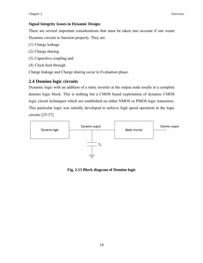
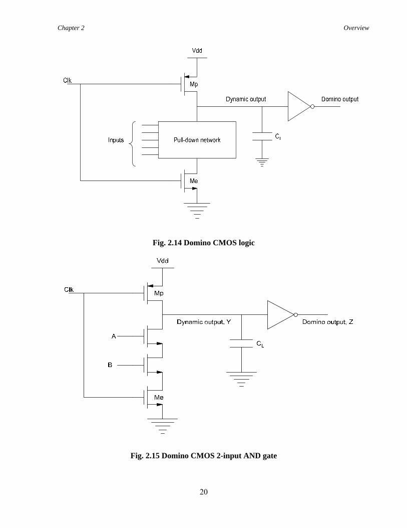
2.4 Domino logic circuits Dynamic logic with an addition of a static inverter at the output node results in a complete
domino logic block. This is nothing but a CMOS based exploitation of dynamic CMOS
logic circuit techniques which are established on either NMOS or PMOS logic transistors.
This particular logic was initially developed to achieve high speed operation in the logic
circuits [25-27].
Fig. 2.13 Block diagram of Domino logic
Chapter 2 Overview
20
Fig. 2.14 Domino CMOS logic
Fig. 2.15 Domino CMOS 2-input AND gate

Chapter 2 Overview
21
Fig. 2.16 Domino CMOS 2-input AND gate simulation
The 2-input domino AND gate shown in Fig. 2.15 is used to illustrate the logical
functionality, the advantage of increased speed, and few challenges involved in using this
Domino CMOS logic family. It is observed that there are two inputs, A and B, along with
the driving element clock signal, Clk. Since it is an implementation of purely a
combinational circuit-AND gate which does not require any clock signal, unlike sequential
logic circuits, the presence of clock signal makes it strange. Domino CMOS logic like
dynamic logic is also a clocked type of logic family in which every single logic gate has
presence of clock signal. If the clock becomes low, then the dynamic node gets charged to
supply voltage, causing the domino output, Z to go low due to the presence of inverter
between these two nodes. Now this mechanism represents that the gate output to go low
logic level once it has been driven high logic level. So this operating period of the block
when the clock signal and output are low is known as the Pre-charge phase. Next phase is
Evaluation phase which starts when clock signal is high. During this Evaluation phase the
actual functional logic is evaluated through Pull Down Network. Therefore the output, Z
may go high if both inputs A and B are high, which results the evaluation or dynamic node
to be driven to a low logic value. The Evaluation phase as mentioned earlier is the actual
functional operating cycle in domino logic circuits with the Pre-charge phase enabling the
succeeding Evaluation phase to occur. The significant application of the presence of clock
Chapter 2 Overview
22
signal in domino logic ensures that the critical path only traverses through NMOS
transistors of Pull Down Network present in the Evaluation phase. One of the advantages
of domino cell is that there is no need for the input signals to drive any PMOS transistor
present in Pull Up Network as the domino cell only switches from low logic level to high
logic level direction.
Now, for a particular instant of current drive, the lack of a PMOS transistor implies
that the effective width of PMOS transistor which loads down its previous stage logic
favors this domino logic over the static logic. Here it is very critical because the key to
very high speed is ensuring that the advantage of high speed can be acquired without
loading down the logic block greatly.
Advantages:
(1) Domino logic circuits allow nominal rail-to-rail swing.
(2) Domino logic circuits comparatively have smaller areas than static CMOS logic
circuits.
(3) Higher operating speeds are possible since parasitic capacitances in cells are reliably
smaller.
(4) Domino logic ensures free glitch operation as each gate can make only single
transition.
Disadvantages:
(1) There is relatively deterioration of noise immunity due to the presence of problems like
unavoidable leakage currents and charge sharing issues.
(2) Relatively large power consumption when compared to the static CMOS logic.
(3) Only non inverting functional structures can be built since there is an inverting buffer
at the dynamic node.
(4) Charge distribution may also be taken care off.

Chapter 2 Overview
23
List of Important Logic Families
• Resistor Transistor Logic (RTL)
• Resistor Capacitor Transistor Logic (RCTL)
• Diode Transistor Logic (DTL)
• Transistor Transistor Logic (TTL)
• Direct Coupled Transistor Logic (DCTL)
• Integrated Injection Logic (IIL)
• High Threshold Logic (HTL)
• Emitter Coupled Logic/Current Mode Logic (ECL/CML)
• Metal Oxide Semiconductor Logic (MOSL)
• Complementary Metal Oxide Semiconductor Logic (CMOSL)
• Pseudo NMOS Logic
• Enhancement NMOS Logic
• Differential Cascode Voltage Swing Logic (DCVSL)
• Pass Transistor Logic (PTL)
• Differential Pass Transistor Logic (DPTL)
• Dynamic CMOS Logic
• Domino CMOS Logic/Domino Logic
2.4.1 Impact on power consumption Power consumption is the one of the predominant constraints which plays a vital role in the
process of designing any digital dynamic logic circuit. Most of the versatile applications in
the microprocessors, digital signal processors and dynamic RAM are based on the
technology platform provided by domino CMOS logic family due to their advantage of
achieving high speed operation with relatively low device count. Of course there might be
inevitable problems like leakage currents and charge sharing issues which normally
degrade the degree of robustness in terms of noise immunity or levels of noise margin of
the domino CMOS logic family. Nevertheless there is significantly huge power dissipation,
in comparison with the other existing static CMOS logic circuits. The continuous down
scaling trend of CMOS technology is making the situation even bitterer from genesis to
genesis. This chapter investigates the functioning of domino logic circuits with the
Chapter 2 Overview
24
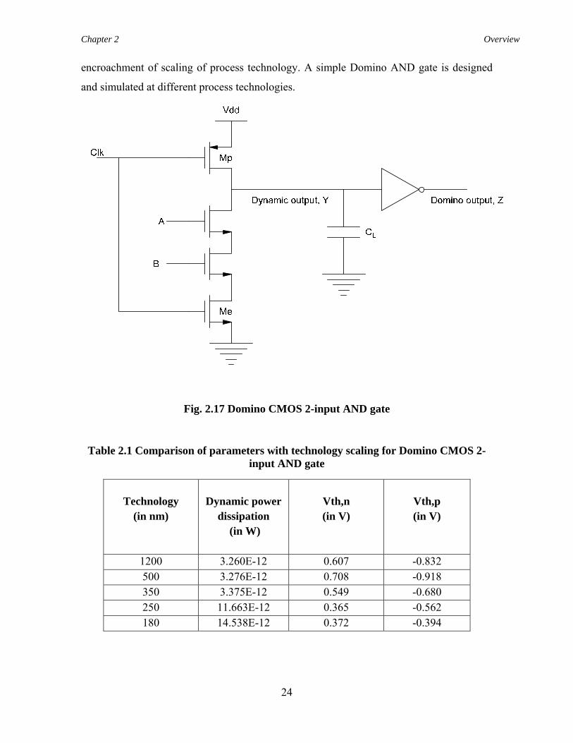
encroachment of scaling of process technology. A simple Domino AND gate is designed
and simulated at different process technologies.
Fig. 2.17 Domino CMOS 2-input AND gate
Table 2.1 Comparison of parameters with technology scaling for Domino CMOS 2-input AND gate
Technology
(in nm)
Dynamic power
dissipation (in W)
Vth,n (in V)
Vth,p (in V)
1200 3.260E-12 0.607 -0.832 500 3.276E-12 0.708 -0.918 350 3.375E-12 0.549 -0.680 250 11.663E-12 0.365 -0.562 180 14.538E-12 0.372 -0.394
Chapter 2 Overview
25
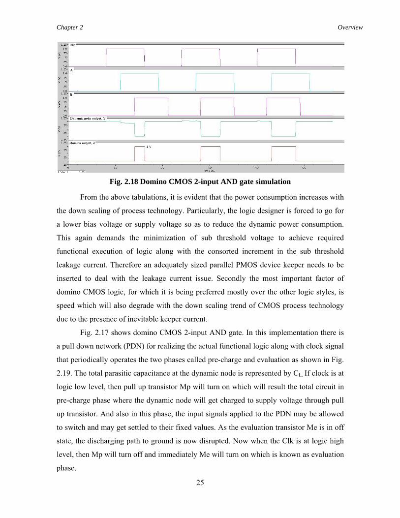
Fig. 2.18 Domino CMOS 2-input AND gate simulation
From the above tabulations, it is evident that the power consumption increases with
the down scaling of process technology. Particularly, the logic designer is forced to go for
a lower bias voltage or supply voltage so as to reduce the dynamic power consumption.
This again demands the minimization of sub threshold voltage to achieve required
functional execution of logic along with the consorted increment in the sub threshold
leakage current. Therefore an adequately sized parallel PMOS device keeper needs to be
inserted to deal with the leakage current issue. Secondly the most important factor of
domino CMOS logic, for which it is being preferred mostly over the other logic styles, is
speed which will also degrade with the down scaling trend of CMOS process technology
due to the presence of inevitable keeper current.
Fig. 2.17 shows domino CMOS 2-input AND gate. In this implementation there is
a pull down network (PDN) for realizing the actual functional logic along with clock signal
that periodically operates the two phases called pre-charge and evaluation as shown in Fig.
2.19. The total parasitic capacitance at the dynamic node is represented by CL. If clock is at
logic low level, then pull up transistor Mp will turn on which will result the total circuit in
pre-charge phase where the dynamic node will get charged to supply voltage through pull
up transistor. And also in this phase, the input signals applied to the PDN may be allowed
to switch and may get settled to their fixed values. As the evaluation transistor Me is in off
state, the discharging path to ground is now disrupted. Now when the Clk is at logic high
level, then Mp will turn off and immediately Me will turn on which is known as evaluation
phase.
Chapter 2 Overview
26
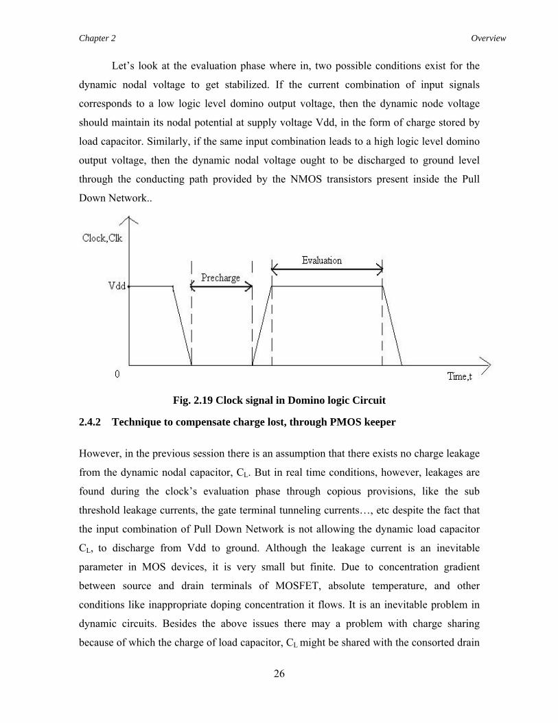
Let’s look at the evaluation phase where in, two possible conditions exist for the
dynamic nodal voltage to get stabilized. If the current combination of input signals
corresponds to a low logic level domino output voltage, then the dynamic node voltage
should maintain its nodal potential at supply voltage Vdd, in the form of charge stored by
load capacitor. Similarly, if the same input combination leads to a high logic level domino
output voltage, then the dynamic nodal voltage ought to be discharged to ground level
through the conducting path provided by the NMOS transistors present inside the Pull
Down Network..
Fig. 2.19 Clock signal in Domino logic Circuit
2.4.2 Technique to compensate charge lost, through PMOS keeper
However, in the previous session there is an assumption that there exists no charge leakage
from the dynamic nodal capacitor, CL. But in real time conditions, however, leakages are
found during the clock’s evaluation phase through copious provisions, like the sub
threshold leakage currents, the gate terminal tunneling currents…, etc despite the fact that
the input combination of Pull Down Network is not allowing the dynamic load capacitor
CL, to discharge from Vdd to ground. Although the leakage current is an inevitable
parameter in MOS devices, it is very small but finite. Due to concentration gradient
between source and drain terminals of MOSFET, absolute temperature, and other
conditions like inappropriate doping concentration it flows. It is an inevitable problem in
dynamic circuits. Besides the above issues there may a problem with charge sharing
because of which the charge of load capacitor, CL might be shared with the consorted drain
Chapter 2 Overview
27
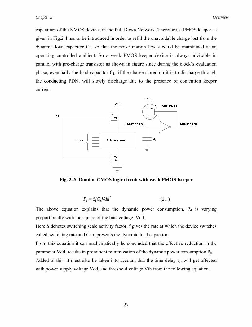
capacitors of the NMOS devices in the Pull Down Network. Therefore, a PMOS keeper as
given in Fig.2.4 has to be introduced in order to refill the unavoidable charge lost from the
dynamic load capacitor CL, so that the noise margin levels could be maintained at an
operating controlled ambient. So a weak PMOS keeper device is always advisable in
parallel with pre-charge transistor as shown in figure since during the clock’s evaluation
phase, eventually the load capacitor CL, if the charge stored on it is to discharge through
the conducting PDN, will slowly discharge due to the presence of contention keeper
current.
Fig. 2.20 Domino CMOS logic circuit with weak PMOS Keeper
2
d LP SfC Vdd= (2.1)
The above equation explains that the dynamic power consumption, Pd is varying
proportionally with the square of the bias voltage, Vdd.
Here S denotes switching scale activity factor, f gives the rate at which the device switches
called switching rate and CL represents the dynamic load capacitor.
From this equation it can mathematically be concluded that the effective reduction in the
parameter Vdd, results in prominent minimization of the dynamic power consumption Pd.
Added to this, it must also be taken into account that the time delay td, will get affected
with power supply voltage Vdd, and threshold voltage Vth from the following equation.

Chapter 2 Overview
28
2
( )T
Ld
H
C VddtK Vd Vd α=
− (2.2)
Here α gives the velocity saturation index whose value is 1.3(approximately 1) for
a short channel device and 2 for a long channel device [11-20]. K denotes the parameter
which is described by the process of CMOS technology. Now let’s take an ideal case from
the equation that in order make time delay td, independent of Vdd, the threshold voltage
VTH, must be set to zero for a short channel device whose approximated value of α is 1.
Thus it gives a striking effect on minimizing the time delay td with the reduction of Vdd
irrespective of VTH. But this assumption is highly impossible as each device possesses non-
zero threshold voltage. Therefore this case is to be optimized. The threshold voltage VTH,
is to be decreased in such a way that time delay td, must not get affected by any means.
This operation again results in the subsequent exponential increment in the sub threshold
leakage current Ileak. Hence in order to compensate this difficulty of getting higher
leakages, the logic design engineer is any way forced to go for a PMOS keeper which is a
bit larger than earlier minimum sized keeper device. Now with this, it gives two possible
conditions for the process of discharging of dynamic load capacitor CL during the
evaluation phase of the clock signal. Firstly, if load capacitor CL is to discharge, then the
entire process will be decelerated due to the keeper device contention current. Secondly, as
long as the contention keeper current is maintaining a greater value than the discharging
current, the load capacitor CL will never get discharged to ground level at all.
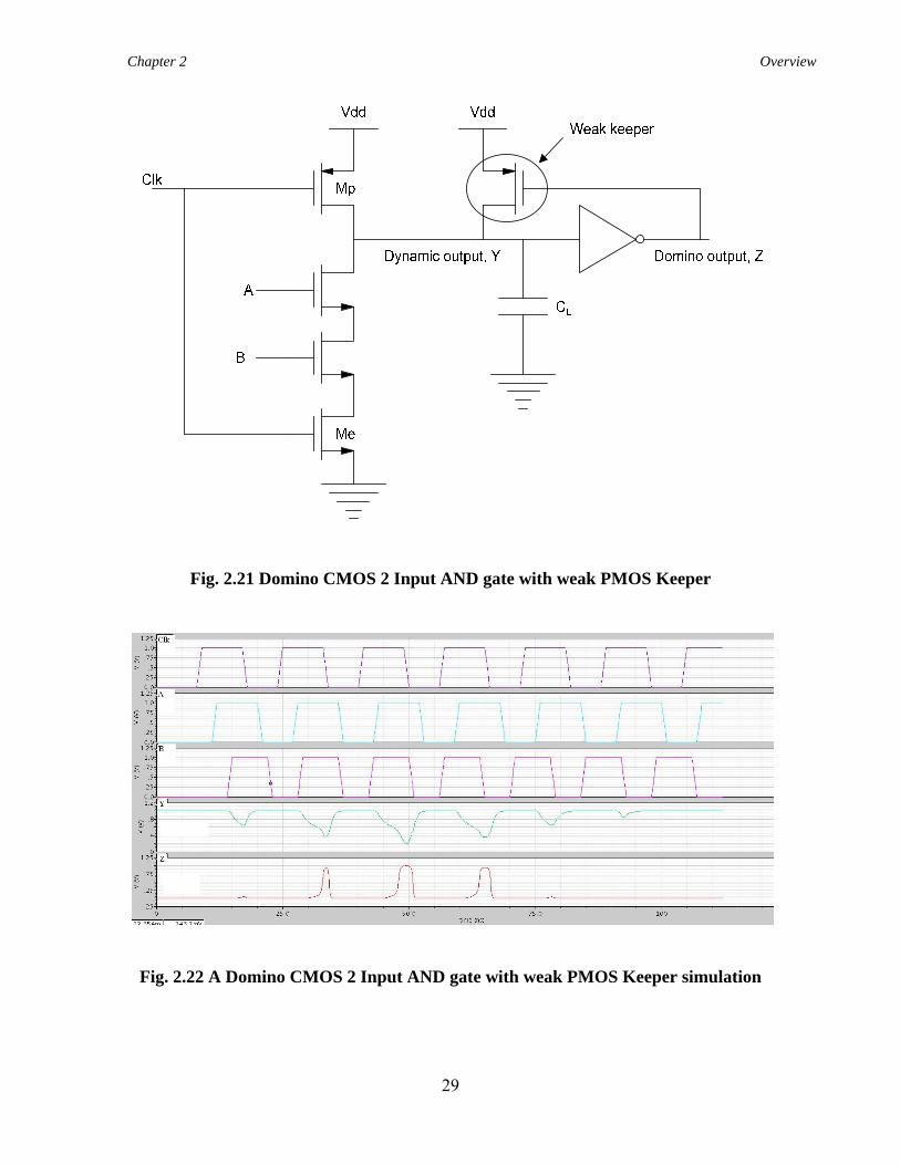
Chapter 2 Overview
29
Fig. 2.21 Domino CMOS 2 Input AND gate with weak PMOS Keeper
Fig. 2.22 A Domino CMOS 2 Input AND gate with weak PMOS Keeper simulation
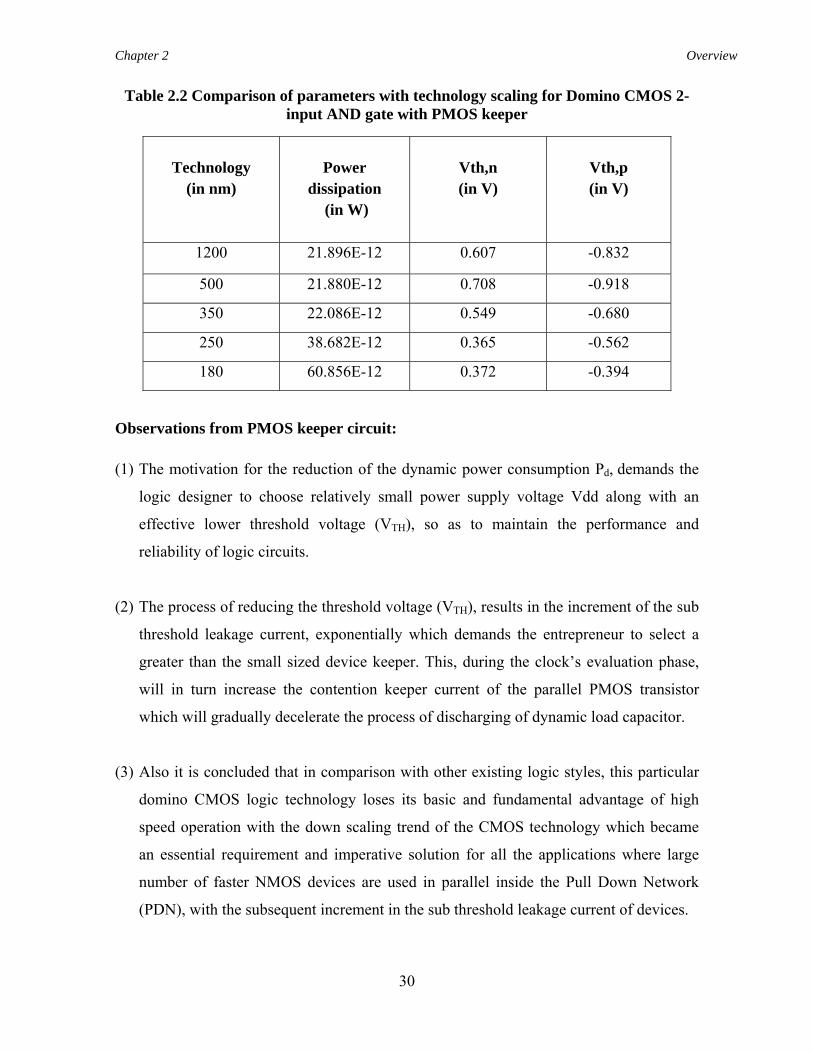
Chapter 2 Overview
30
Table 2.2 Comparison of parameters with technology scaling for Domino CMOS 2-input AND gate with PMOS keeper
Technology
(in nm)
Power
dissipation (in W)
Vth,n (in V)
Vth,p (in V)
1200 21.896E-12 0.607 -0.832
500 21.880E-12 0.708 -0.918
350 22.086E-12 0.549 -0.680
250 38.682E-12 0.365 -0.562
180 60.856E-12 0.372 -0.394
Observations from PMOS keeper circuit:
(1) The motivation for the reduction of the dynamic power consumption Pd, demands the
logic designer to choose relatively small power supply voltage Vdd along with an
effective lower threshold voltage (VTH), so as to maintain the performance and
reliability of logic circuits.
(2) The process of reducing the threshold voltage (VTH), results in the increment of the sub
threshold leakage current, exponentially which demands the entrepreneur to select a
greater than the small sized device keeper. This, during the clock’s evaluation phase,
will in turn increase the contention keeper current of the parallel PMOS transistor
which will gradually decelerate the process of discharging of dynamic load capacitor.
(3) Also it is concluded that in comparison with other existing logic styles, this particular
domino CMOS logic technology loses its basic and fundamental advantage of high
speed operation with the down scaling trend of the CMOS technology which became
an essential requirement and imperative solution for all the applications where large
number of faster NMOS devices are used in parallel inside the Pull Down Network
(PDN), with the subsequent increment in the sub threshold leakage current of devices.
Chapter 2 Overview
31
2.5 Conclusion
Therefore, this chapter has given overview of standard logic styles in brief and
introduced the dynamic logic followed by domino logic circuits with description. The
research area is primarily focused on present working environment-Domino logic from a
broader angle. Description of various circuit styles along with their advantages and
disadvantages is illustrated. In addition to this, the functioning of domino logic with the
encroachment of down scaling of process technology is investigated and this analysis
reveals that with deep sub-micron, more power is consumed. This is presented in Table
2.1. Technique, which uses a PMOS keeper at dynamic node, to alleviate inevitable
charge-lost is reviewed and corresponding simulation result is presented in Table 2.2. A
detailed review on domino logic is conducted and issues related to domino logic are
brought out that facilitated us proceeding to the next chapter.
Chapter 3 Novel Domino Logic topologies
32
CHAPTER 3 NOVEL DOMINO LOGIC TOPOLOGIES
3.1 Introduction Domino CMOS logic circuit family explores ample applications in the process of
designing high performance circuits because of its increased speed and reduced
implementation area, despite its high noise sensitivity for which the sub-threshold leakage
current through the evaluation network is the prime factor. The issue becomes much more
complex with constant down scaling of process technology [30-35].
Due to the fast-growing trend of down scaling of the process technology especially in the
field of deep sub-micron, noise-tolerance has become one of the primary concerning issues
in the design of VLSI chip manufacturing field. This noise in the digital VLSI integrated
circuit design normally relates to the fluctuation which may cause the variation of a nodal
voltage from its base value. There have been distinctly various sources of noise in the
deep-submicron regime which are typically associated with crosstalk, charge sharing,
inevitable leakage currents and minute variations of the supply voltage from its base value.
The leakage current is the most predominant factor which is found to be rising
exponentially with the down scaling of process technology [31, 32]. However, the bias
voltage is to be reduced to limit dynamic power consumption. Simultaneously, the down
scaling of the threshold voltage (VTH) of the MOS devices to ensure high performance
causes the sub-threshold leakage current to increase exponentially, as it is dependent on -
VTH. Besides this, there is a definite increment in the gate leakage current with the
subsequent reduction of the gate oxide thickness due to the impact of gate oxide carrier
tunneling.
Therefore, to achieve high performance in various aspects, several design techniques are
widely exploited. Domino logic design is one amongst them which is faster than static
counterpart. Also these gates are much more compact, exclusively when dealt with circuits
with wide fan-in gates such as multiplexers, which became the process of choice of high
performance in microprocessors and digital signal processors. Added to this, domino logic
gates exhibit high noise sensitivity when compared with static CMOS logic gates due to
the low threshold voltage, which is almost equal to VTH of NMOS transistors in the pull-
Chapter 3 Novel Domino Logic topologies
33
down network. Noise sensitivity is one of the major concerning issues in recent days,
distinctly in the process of designing circuits with wide fan-in gates.
Versatile techniques have been illustrated to alleviate the noise leakage issues of several
wide fan-in domino logic gates [33-40] and there is an improvement of the noise
robustness. Furthermore, the reduction in speed and the increment in power dissipation
became more tactile with continuous down scaling of process technology.
Novel techniques are proposed in this chapter to increase the noise robustness of domino
logic gates with low power and reduced leakages. In order to demonstrate the proficiency
of proposed scheme, comparisons are made with existing techniques and it is illustrated
that from the perception of Power Delay Product (PDP), the proposed techniques exhibit
PDP lower than that of the existing techniques. Simulation results reveal that the proposed
technique can attain high degree of noise robustness with low power and low leakages in
CMOS 90nm technology platform used for analyzing wide fan-in logic circuits. Also the
predominant noise metric parameters such as UNG and ANTE are significantly improved
in proposed techniques. To probe further, dealing with sub-threshold leakages, the
proposed schemes effectively minimize the leakage power.
In section 2, several existing domino logic schemes dealing with noise tolerance
associated with leakages and power dissipation are discussed. Section 3 demonstrates the
proposed novel domino logic techniques. Analyzing the noise metric parameters like UNG
and ANTE is executed in section 4. Section 5 describes the process corner analysis.
Simulation results through tabulations and graphs along with discussion are given in
section 6 and concluding remarks are made in section 7.
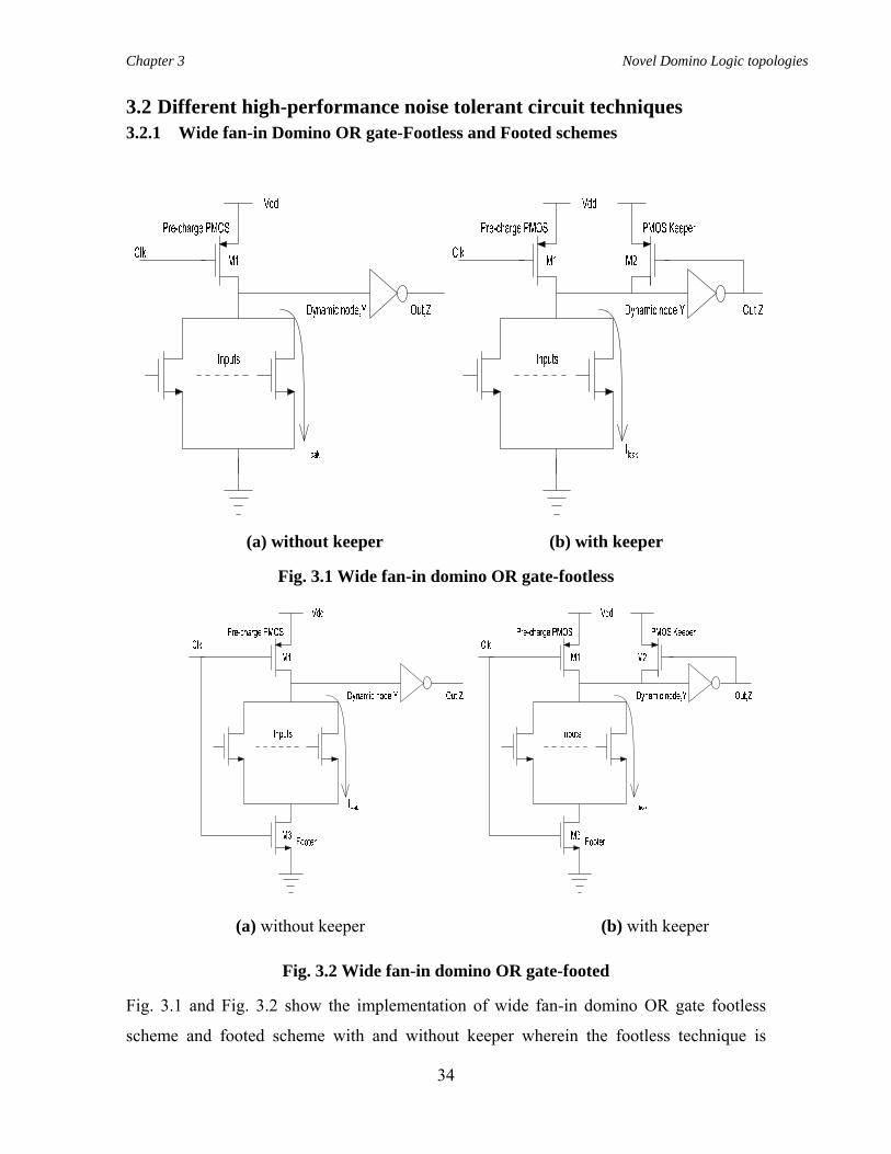
Chapter 3 Novel Domino Logic topologies
34
3.2 Different high-performance noise tolerant circuit techniques 3.2.1 Wide fan-in Domino OR gate-Footless and Footed schemes
(a) without keeper (b) with keeper
Fig. 3.1 Wide fan-in domino OR gate-footless
(a) without keeper (b) with keeper
Fig. 3.2 Wide fan-in domino OR gate-footed
Fig. 3.1 and Fig. 3.2 show the implementation of wide fan-in domino OR gate footless
scheme and footed scheme with and without keeper wherein the footless technique is

Chapter 3 Novel Domino Logic topologies
35
frequently exploited in high-performance logic circuits because of its quick discharging
process of the dynamic node, with minimal capacitive load of the Clk signal that manages
the entire domino logic operation [30-40].
During the pre-charge phase (when Clk is low) the dynamic node gets charged to supply
voltage Vdd through pre-charge PMOS transistor. When the Clk becomes high the
evaluation phase starts where the actual logic function is being evaluated by elaborating
the input signals through gate terminal during which the dynamic node doesn’t possess any
connection to Vdd rail through pre-charge PMOS device.
Employing keeper technique is an advantage to avoid the charge lost from dynamic node
when needed a strong one at this node [45]. There may be a chance of getting deterioration
of strength of voltage at dynamic node due to the inevitable flow of sub-threshold leakage
currents through pull-down network in Clk’s evaluation mode and hence this voltage drop
needs to be recompensed by other means in order to stabilize the node. This could be
achieved by employing PMOS keeper device between the dynamic node and supply rail
whose gate terminal is driven by domino output. As long as domino output Z, is low,
keeper charges dynamic nodal voltage up to Vdd which may have been forced to go for
wrong discharge by the flow of sub-threshold leakage current through pull-down network
even if all the inputs of pull-down network are low. This effect becomes much more severe
with the occurrence of noise pulse or glitch at any of the input nodes. However, the noise
voltage impulse triggers notable effects such as the exponential rise of sub-threshold
leakage current through the pull-down network with the abrupt fluctuation of gate-to-
source voltage (VGS) which leads to forceful discharge of the dynamic node. Also there is a
reduction in gate leakage current, because of reduction of VDG with VGS increasing, which
is almost irrelevant when compared to the significant increment of the sub-threshold
leakage current. In reality, the impact of VDG on gate leakage current is not as much
significant as the effect of VGS on the sub-threshold leakage current. Hence there is
troublesome mechanism associated with discharge of dynamic node owing to the existence
of noise glitch at the input nodes of pull-down network. Besides these issues, the
secondary cause that forces dynamic node to discharge wrongly during the evaluation
phase is an abrupt change at the ground level nodal voltage since if at all exists a negative
pulse, at the ground level, it may increase the effective VGS of NMOS devices of the pull-
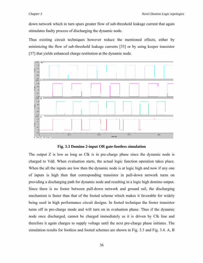
Chapter 3 Novel Domino Logic topologies
36
down network which in turn spurs greater flow of sub-threshold leakage current that again
stimulates faulty process of discharging the dynamic node.
Thus existing circuit techniques however reduce the mentioned effects, either by
minimizing the flow of sub-threshold leakage currents [33] or by using keeper transistor
[37] that yields enhanced charge restitution at the dynamic node.
Fig. 3.3 Domino 2-input OR gate-footless simulation
The output Z is low as long as Clk is in pre-charge phase since the dynamic node is
charged to Vdd. When evaluation starts, the actual logic function operation takes place.
When the all the inputs are low then the dynamic node is at logic high and now if any one
of inputs is high then that corresponding transistor in pull-down network turns on
providing a discharging path for dynamic node and resulting in a logic high domino output.
Since there is no footer between pull-down network and ground rail, the discharging
mechanism is faster than that of the footed scheme which makes it favorable for widely
being used in high performance circuit designs. In footed technique the footer transistor
turns off in pre-charge mode and will turn on in evaluation phase. Thus if the dynamic
node once discharged, cannot be charged immediately as it is driven by Clk line and
therefore it again charges to supply voltage until the next pre-charge phase initiates. The
simulation results for footless and footed schemes are shown in Fig. 3.3 and Fig. 3.4. A, B
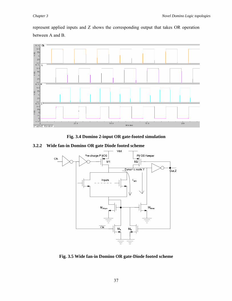
Chapter 3 Novel Domino Logic topologies
37
represent applied inputs and Z shows the corresponding output that takes OR operation
between A and B.
Fig. 3.4 Domino 2-input OR gate-footed simulation
3.2.2 Wide fan-in Domino OR gate Diode footed scheme
Fig. 3.5 Wide fan-in Domino OR gate-Diode footed scheme

Chapter 3 Novel Domino Logic topologies
38
Fig. 3.6 Domino 2-input OR gate-Diode footed scheme simulation
A Wide fan-in Domino OR gate Diode footed scheme is shown in Fig. 3.5 [40].
The flow of sub-threshold leakage current in the evaluation phase through pull-down
network is controlled by the diode footer transistor-MDiode, through the phenomenon called
stack effect [40-55]. The leakage current through pull-down network constitutes a nominal
voltage drop across the diode footer which makes the VGS of the ‘off’ NMOS devices
inside the pull-down network negative and thereby reducing the flow of sub-threshold
leakage current exponentially. Also the diode voltage drop increases the body effect of the
pull-down devices, which helps in the subsequent reduction of sub-threshold leakage
reduction [49]. The simulation of domino 2-input OR gate using diode footed scheme is
given in Fig. 3.6. Besides this, the diode footer device doubles the threshold voltage of gate
and hence the new switching threshold voltage becomes 2Vth-n. Higher the gate switching
threshold voltage, greater the noise immunity. But this in turn, as a drawback of this
technique, raises equivalent resistance of the evaluation path of pull-down network by the
diode footer that eventually makes the gate slower. An alternative discharging path has
been established and also assures high performance by the mirror network which consists
of the NMOS devices MA, MB and MMirror. The cause behind the deterioration in the
performance is the decrement of evaluation current by the diode footer. In order to stabilize
this evaluation current, the mirror transistor is connected as shown in Fig. 3.5. MMirror is
used for mirroring action of evaluation current and is drained from the dynamic node.
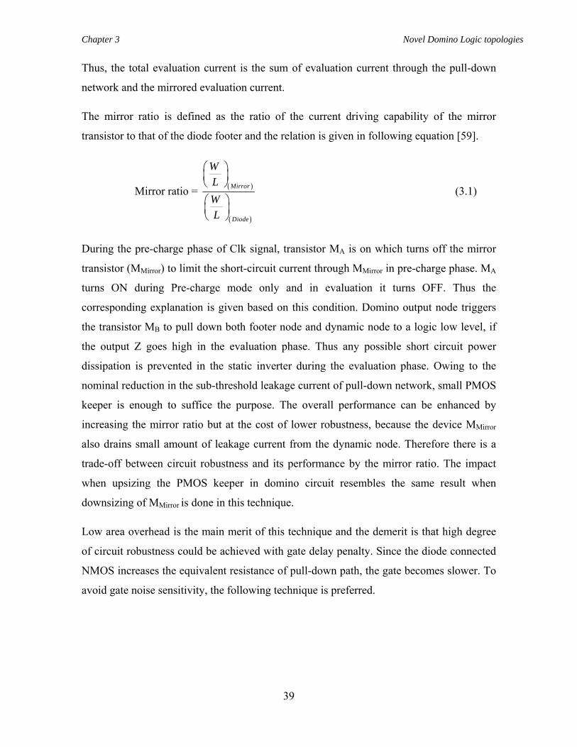
Chapter 3 Novel Domino Logic topologies
39
Thus, the total evaluation current is the sum of evaluation current through the pull-down
network and the mirrored evaluation current.
The mirror ratio is defined as the ratio of the current driving capability of the mirror
transistor to that of the diode footer and the relation is given in following equation [59].
Mirror ratio = ( )
( )
Mirror
Diode
WLWL
⎛ ⎞⎜ ⎟⎝ ⎠⎛ ⎞⎜ ⎟⎝ ⎠
(3.1)
During the pre-charge phase of Clk signal, transistor MA is on which turns off the mirror
transistor (MMirror) to limit the short-circuit current through MMirror in pre-charge phase. MA
turns ON during Pre-charge mode only and in evaluation it turns OFF. Thus the
corresponding explanation is given based on this condition. Domino output node triggers
the transistor MB to pull down both footer node and dynamic node to a logic low level, if
the output Z goes high in the evaluation phase. Thus any possible short circuit power
dissipation is prevented in the static inverter during the evaluation phase. Owing to the
nominal reduction in the sub-threshold leakage current of pull-down network, small PMOS
keeper is enough to suffice the purpose. The overall performance can be enhanced by
increasing the mirror ratio but at the cost of lower robustness, because the device MMirror
also drains small amount of leakage current from the dynamic node. Therefore there is a
trade-off between circuit robustness and its performance by the mirror ratio. The impact
when upsizing the PMOS keeper in domino circuit resembles the same result when
downsizing of MMirror is done in this technique.
Low area overhead is the main merit of this technique and the demerit is that high degree
of circuit robustness could be achieved with gate delay penalty. Since the diode connected
NMOS increases the equivalent resistance of pull-down path, the gate becomes slower. To
avoid gate noise sensitivity, the following technique is preferred.
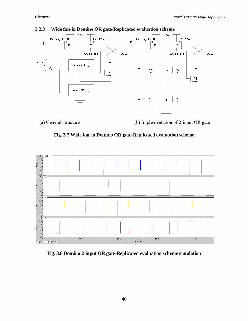
Chapter 3 Novel Domino Logic topologies
40
3.2.3 Wide fan-in Domino OR gate-Replicated evaluation scheme
(a) General structure (b) Implementation of 2-input OR gate
Fig. 3.7 Wide fan-in Domino OR gate-Replicated evaluation scheme
Fig. 3.8 Domino 2-input OR gate-Replicated evaluation scheme simulation
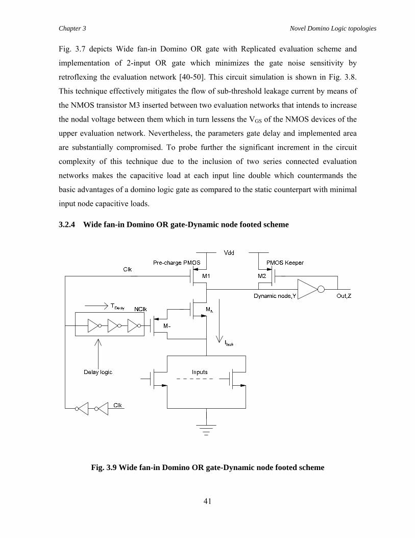
Chapter 3 Novel Domino Logic topologies
41
Fig. 3.7 depicts Wide fan-in Domino OR gate with Replicated evaluation scheme and
implementation of 2-input OR gate which minimizes the gate noise sensitivity by
retroflexing the evaluation network [40-50]. This circuit simulation is shown in Fig. 3.8.
This technique effectively mitigates the flow of sub-threshold leakage current by means of
the NMOS transistor M3 inserted between two evaluation networks that intends to increase
the nodal voltage between them which in turn lessens the VGS of the NMOS devices of the
upper evaluation network. Nevertheless, the parameters gate delay and implemented area
are substantially compromised. To probe further the significant increment in the circuit
complexity of this technique due to the inclusion of two series connected evaluation
networks makes the capacitive load at each input line double which countermands the
basic advantages of a domino logic gate as compared to the static counterpart with minimal
input node capacitive loads.
3.2.4 Wide fan-in Domino OR gate-Dynamic node footed scheme
Fig. 3.9 Wide fan-in Domino OR gate-Dynamic node footed scheme
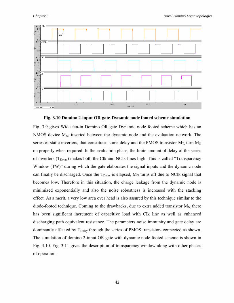
Chapter 3 Novel Domino Logic topologies
42
Fig. 3.10 Domino 2-input OR gate-Dynamic node footed scheme simulation
Fig. 3.9 gives Wide fan-in Domino OR gate Dynamic node footed scheme which has an
NMOS device MN, inserted between the dynamic node and the evaluation network. The
series of static inverters, that constitutes some delay and the PMOS transistor MT, turn MN
on properly when required. In the evaluation phase, the finite amount of delay of the series
of inverters (TDelay) makes both the Clk and NClk lines high. This is called “Transparency
Window (TW)” during which the gate elaborates the signal inputs and the dynamic node
can finally be discharged. Once the TDelay is elapsed, MN turns off due to NClk signal that
becomes low. Therefore in this situation, the charge leakage from the dynamic node is
minimized exponentially and also the noise robustness is increased with the stacking
effect. As a merit, a very low area over head is also assured by this technique similar to the
diode-footed technique. Coming to the drawbacks, due to extra added transistor MN, there
has been significant increment of capacitive load with Clk line as well as enhanced
discharging path equivalent resistance. The parameters noise immunity and gate delay are
dominantly affected by TDelay through the series of PMOS transistors connected as shown.
The simulation of domino 2-input OR gate with dynamic node footed scheme is shown in
Fig. 3.10. Fig. 3.11 gives the description of transparency window along with other phases
of operation.
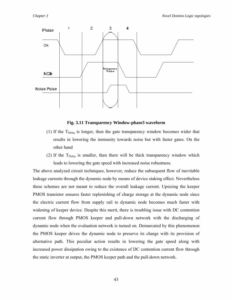
Chapter 3 Novel Domino Logic topologies
43
Fig. 3.11 Transparency Window-phase3 waveform
(1) If the TDelay is longer, then the gate transparency window becomes wider that
results in lowering the immunity towards noise but with faster gates. On the
other hand
(2) If the TDelay is smaller, then there will be thick transparency window which
leads to lowering the gate speed with increased noise robustness.
The above analyzed circuit techniques, however, reduce the subsequent flow of inevitable
leakage currents through the dynamic node by means of device staking effect. Nevertheless
these schemes are not meant to reduce the overall leakage current. Upsizing the keeper
PMOS transistor ensures faster replenishing of charge storage at the dynamic node since
the electric current flow from supply rail to dynamic node becomes much faster with
widening of keeper device. Despite this merit, there is troubling issue with DC contention
current flow through PMOS keeper and pull-down network with the discharging of
dynamic node when the evaluation network is turned on. Demarcated by this phenomenon
the PMOS keeper drives the dynamic node to preserve its charge with its provision of
alternative path. This peculiar action results in lowering the gate speed along with
increased power dissipation owing to the existence of DC contention current flow through
the static inverter at output, the PMOS keeper path and the pull-down network.
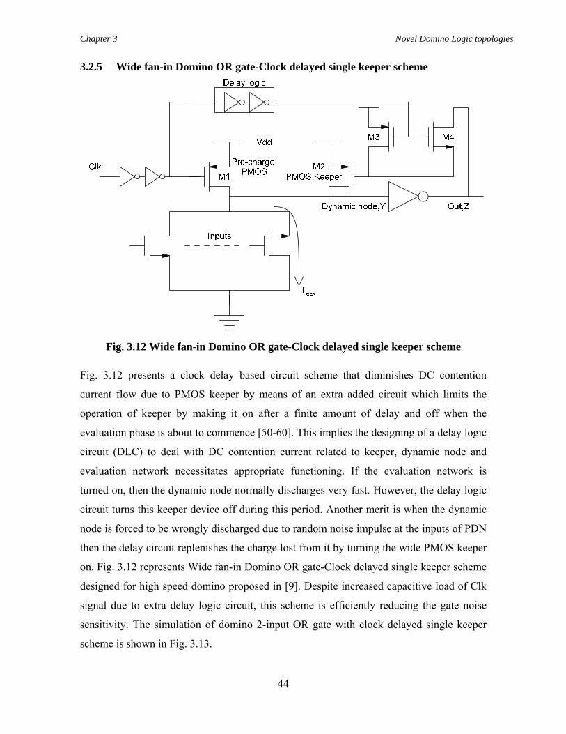
Chapter 3 Novel Domino Logic topologies
44
3.2.5 Wide fan-in Domino OR gate-Clock delayed single keeper scheme
Fig. 3.12 Wide fan-in Domino OR gate-Clock delayed single keeper scheme
Fig. 3.12 presents a clock delay based circuit scheme that diminishes DC contention
current flow due to PMOS keeper by means of an extra added circuit which limits the
operation of keeper by making it on after a finite amount of delay and off when the
evaluation phase is about to commence [50-60]. This implies the designing of a delay logic
circuit (DLC) to deal with DC contention current related to keeper, dynamic node and
evaluation network necessitates appropriate functioning. If the evaluation network is
turned on, then the dynamic node normally discharges very fast. However, the delay logic
circuit turns this keeper device off during this period. Another merit is when the dynamic
node is forced to be wrongly discharged due to random noise impulse at the inputs of PDN
then the delay circuit replenishes the charge lost from it by turning the wide PMOS keeper
on. Fig. 3.12 represents Wide fan-in Domino OR gate-Clock delayed single keeper scheme
designed for high speed domino proposed in [9]. Despite increased capacitive load of Clk
signal due to extra delay logic circuit, this scheme is efficiently reducing the gate noise
sensitivity. The simulation of domino 2-input OR gate with clock delayed single keeper
scheme is shown in Fig. 3.13.
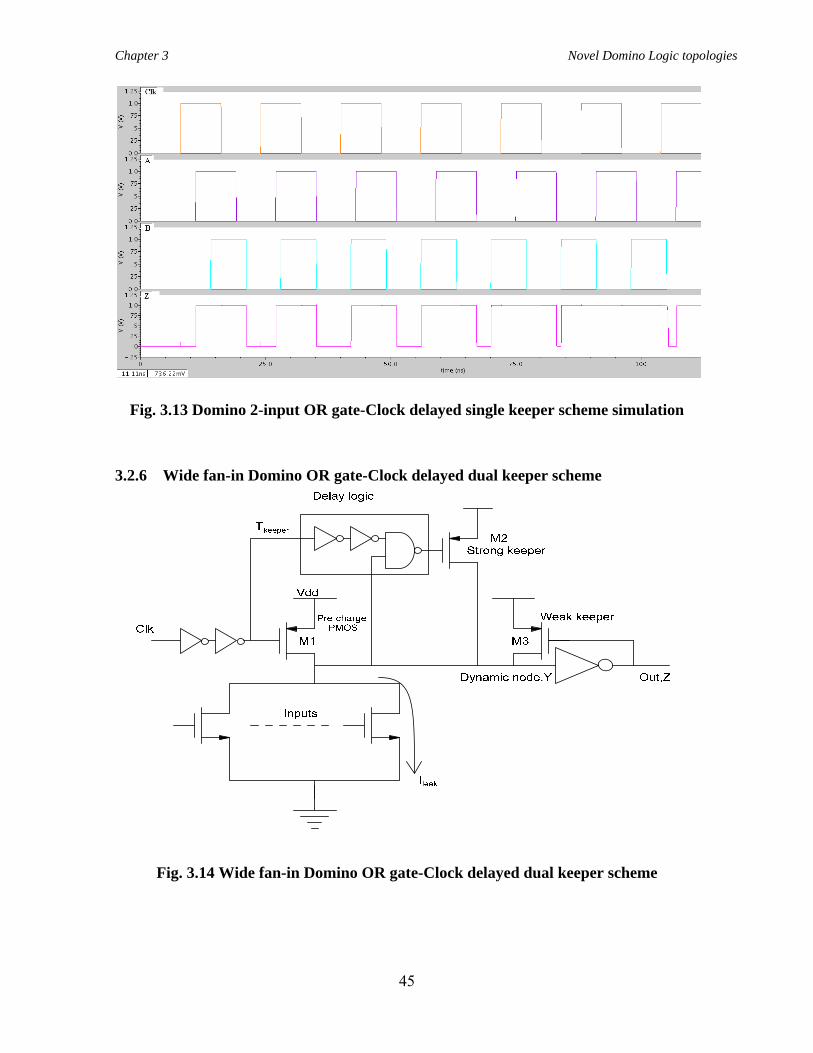
Chapter 3 Novel Domino Logic topologies
45
Fig. 3.13 Domino 2-input OR gate-Clock delayed single keeper scheme simulation
3.2.6 Wide fan-in Domino OR gate-Clock delayed dual keeper scheme
Fig. 3.14 Wide fan-in Domino OR gate-Clock delayed dual keeper scheme
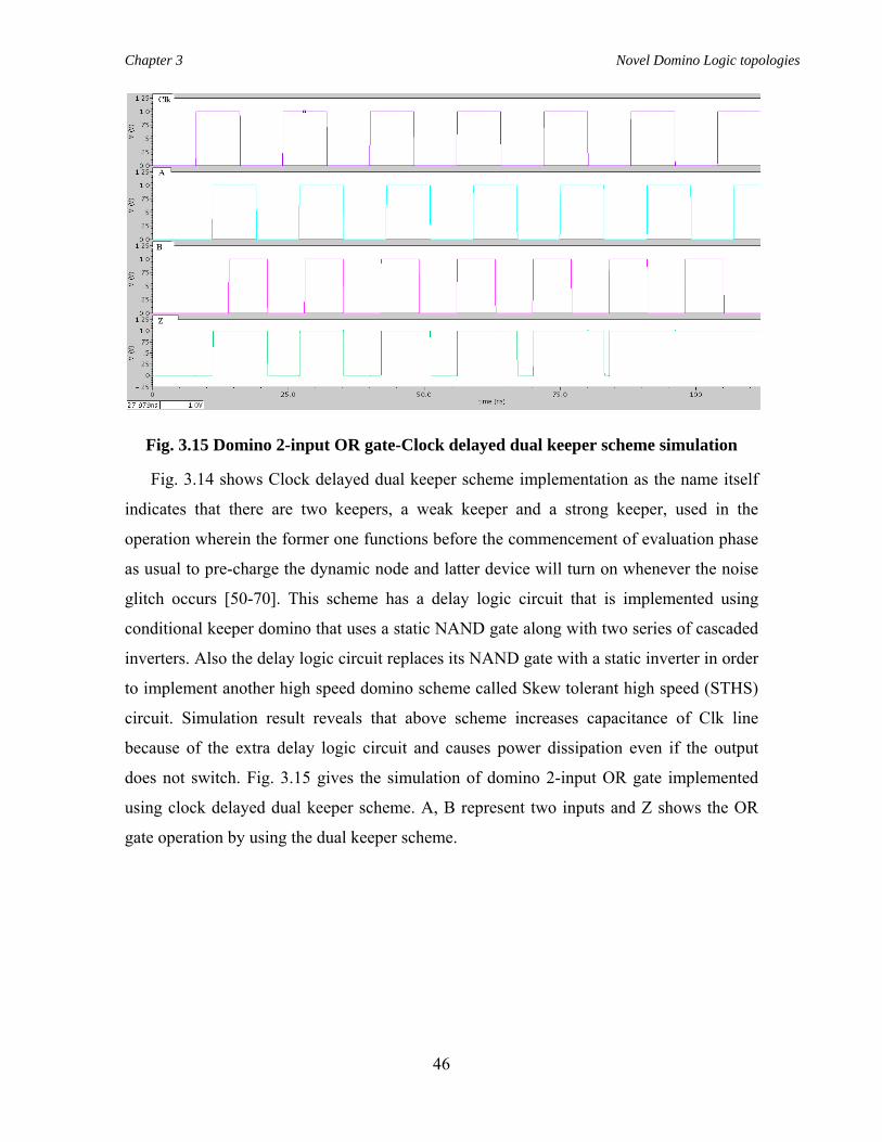
Chapter 3 Novel Domino Logic topologies
46
Fig. 3.15 Domino 2-input OR gate-Clock delayed dual keeper scheme simulation
Fig. 3.14 shows Clock delayed dual keeper scheme implementation as the name itself
indicates that there are two keepers, a weak keeper and a strong keeper, used in the
operation wherein the former one functions before the commencement of evaluation phase
as usual to pre-charge the dynamic node and latter device will turn on whenever the noise
glitch occurs [50-70]. This scheme has a delay logic circuit that is implemented using
conditional keeper domino that uses a static NAND gate along with two series of cascaded
inverters. Also the delay logic circuit replaces its NAND gate with a static inverter in order
to implement another high speed domino scheme called Skew tolerant high speed (STHS)
circuit. Simulation result reveals that above scheme increases capacitance of Clk line
because of the extra delay logic circuit and causes power dissipation even if the output
does not switch. Fig. 3.15 gives the simulation of domino 2-input OR gate implemented
using clock delayed dual keeper scheme. A, B represent two inputs and Z shows the OR
gate operation by using the dual keeper scheme.
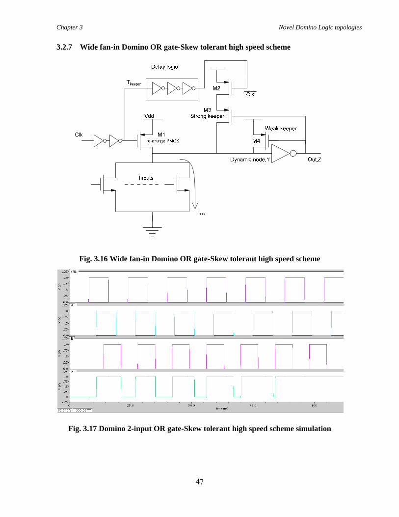
Chapter 3 Novel Domino Logic topologies
47
3.2.7 Wide fan-in Domino OR gate-Skew tolerant high speed scheme
Fig. 3.16 Wide fan-in Domino OR gate-Skew tolerant high speed scheme
Fig. 3.17 Domino 2-input OR gate-Skew tolerant high speed scheme simulation
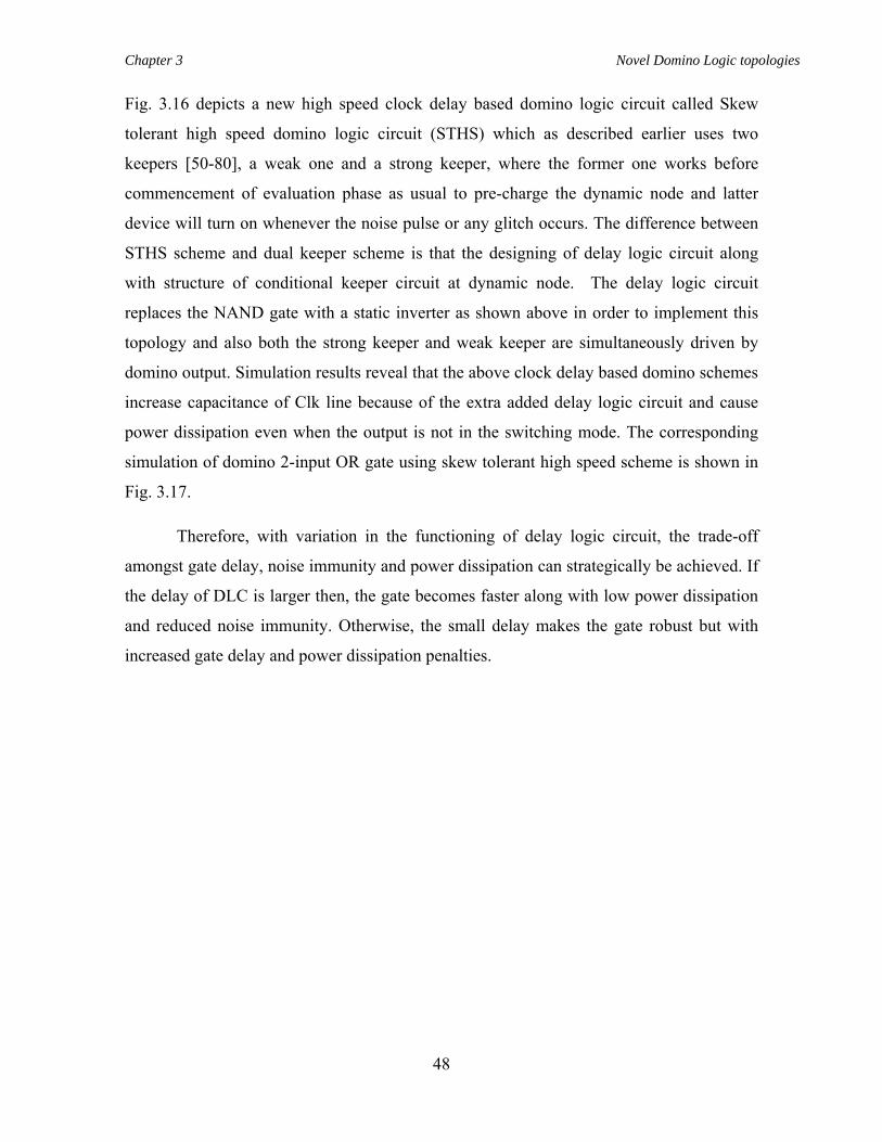
Chapter 3 Novel Domino Logic topologies
48
Fig. 3.16 depicts a new high speed clock delay based domino logic circuit called Skew
tolerant high speed domino logic circuit (STHS) which as described earlier uses two
keepers [50-80], a weak one and a strong keeper, where the former one works before
commencement of evaluation phase as usual to pre-charge the dynamic node and latter
device will turn on whenever the noise pulse or any glitch occurs. The difference between
STHS scheme and dual keeper scheme is that the designing of delay logic circuit along
with structure of conditional keeper circuit at dynamic node. The delay logic circuit
replaces the NAND gate with a static inverter as shown above in order to implement this
topology and also both the strong keeper and weak keeper are simultaneously driven by
domino output. Simulation results reveal that the above clock delay based domino schemes
increase capacitance of Clk line because of the extra added delay logic circuit and cause
power dissipation even when the output is not in the switching mode. The corresponding
simulation of domino 2-input OR gate using skew tolerant high speed scheme is shown in
Fig. 3.17.
Therefore, with variation in the functioning of delay logic circuit, the trade-off
amongst gate delay, noise immunity and power dissipation can strategically be achieved. If
the delay of DLC is larger then, the gate becomes faster along with low power dissipation
and reduced noise immunity. Otherwise, the small delay makes the gate robust but with
increased gate delay and power dissipation penalties.
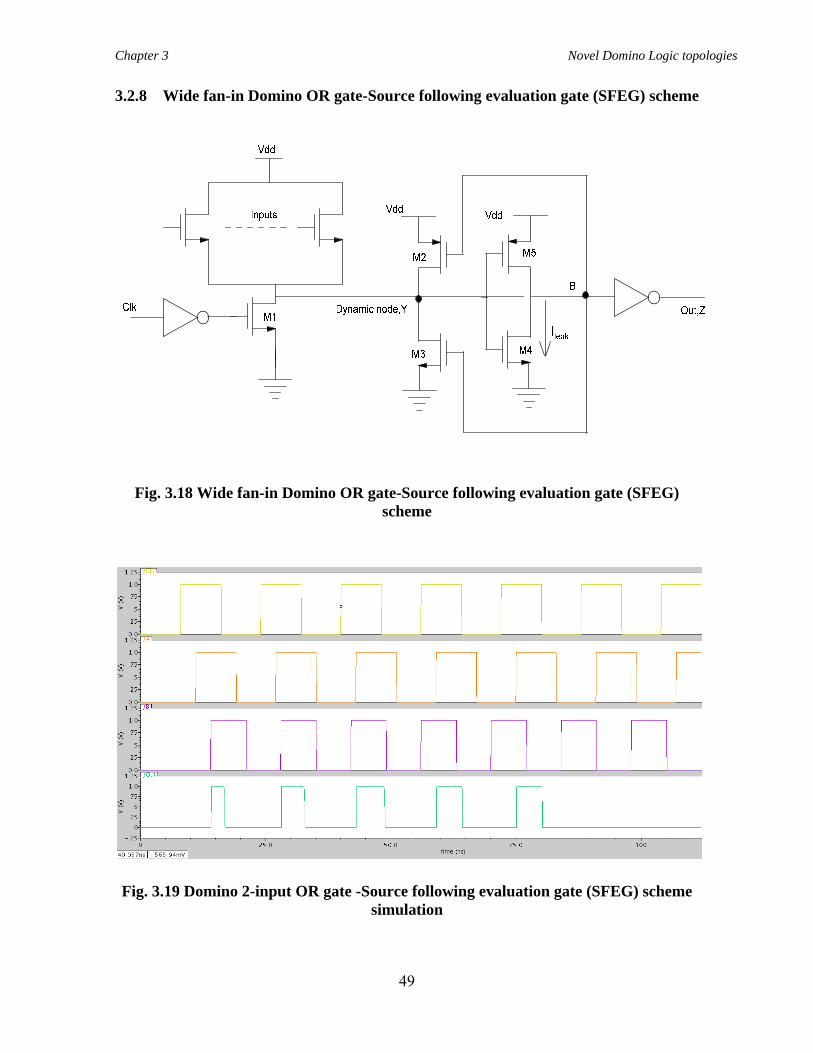
Chapter 3 Novel Domino Logic topologies
49
3.2.8 Wide fan-in Domino OR gate-Source following evaluation gate (SFEG) scheme
Fig. 3.18 Wide fan-in Domino OR gate-Source following evaluation gate (SFEG) scheme
Fig. 3.19 Domino 2-input OR gate -Source following evaluation gate (SFEG) scheme simulation
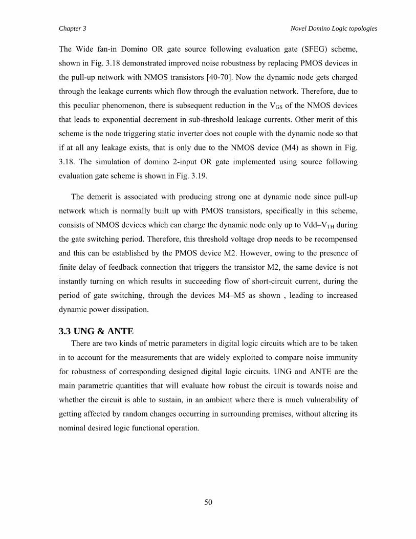
Chapter 3 Novel Domino Logic topologies
50
The Wide fan-in Domino OR gate source following evaluation gate (SFEG) scheme,
shown in Fig. 3.18 demonstrated improved noise robustness by replacing PMOS devices in
the pull-up network with NMOS transistors [40-70]. Now the dynamic node gets charged
through the leakage currents which flow through the evaluation network. Therefore, due to
this peculiar phenomenon, there is subsequent reduction in the VGS of the NMOS devices
that leads to exponential decrement in sub-threshold leakage currents. Other merit of this
scheme is the node triggering static inverter does not couple with the dynamic node so that
if at all any leakage exists, that is only due to the NMOS device (M4) as shown in Fig.
3.18. The simulation of domino 2-input OR gate implemented using source following
evaluation gate scheme is shown in Fig. 3.19.
The demerit is associated with producing strong one at dynamic node since pull-up
network which is normally built up with PMOS transistors, specifically in this scheme,
consists of NMOS devices which can charge the dynamic node only up to Vdd–VTH during
the gate switching period. Therefore, this threshold voltage drop needs to be recompensed
and this can be established by the PMOS device M2. However, owing to the presence of
finite delay of feedback connection that triggers the transistor M2, the same device is not
instantly turning on which results in succeeding flow of short-circuit current, during the
period of gate switching, through the devices M4–M5 as shown , leading to increased
dynamic power dissipation.
3.3 UNG & ANTE There are two kinds of metric parameters in digital logic circuits which are to be taken
in to account for the measurements that are widely exploited to compare noise immunity
for robustness of corresponding designed digital logic circuits. UNG and ANTE are the
main parametric quantities that will evaluate how robust the circuit is towards noise and
whether the circuit is able to sustain, in an ambient where there is much vulnerability of
getting affected by random changes occurring in surrounding premises, without altering its
nominal desired logic functional operation.
Chapter 3 Novel Domino Logic topologies
51
Unity Noise Gain (UNG):
It is the amplitude of the noise pulse at the input node which causes the glitch or dynamic
hazard with the same amplitude at the output node. As the name implies that there is a gain
of voltage amplitude of output glitch to the voltage amplitude of input noise pulse and that
gain factor is required to be unity in order to possess a high degree of robustness. Closer
the voltage gain value towards unity (one), higher the noise immunity or robustness of the
circuit.
UNG = {Vnoise; when Vnoise = Vout}
Average Noise Threshold Energy (ANTE):
It is the average input noise energy that the circuit can tolerate without altering its normal
logical functioning. Also it is the UNG measurement but with an average calculation for
few set of values within the conditional boundaries. Larger the ANTE, greater the circuit
robustness.
ANTE = 1K
⎛ ⎞⎜ ⎟⎝ ⎠
2n o i s e n o i s eV T∑
Where noiseV = Amplitude of input noise pulse,
noiseT = Pulse width of input noise pulse and
K = Number of iterations or observations.
For the measurement of these quantities, noise pulses are applied at the input nodes of pull-
down network in the evaluation period of clock signal, and the applied noise pulses possess
certain amplitude with pulse width and time duration. There are two methods to take the
measurement of output glitch by changing the shape of input noise pulse in different
aspects. Varying the voltage amplitude of input noise pulse randomly by keeping its pulse
width constant, to observe the corresponding changes occurring in the glitch is one method
to calculate the UNG. Otherwise keeping the amplitude of input noise pulse voltage fixed
at one level and computing the respective changes in the amplitude of output glitch for all
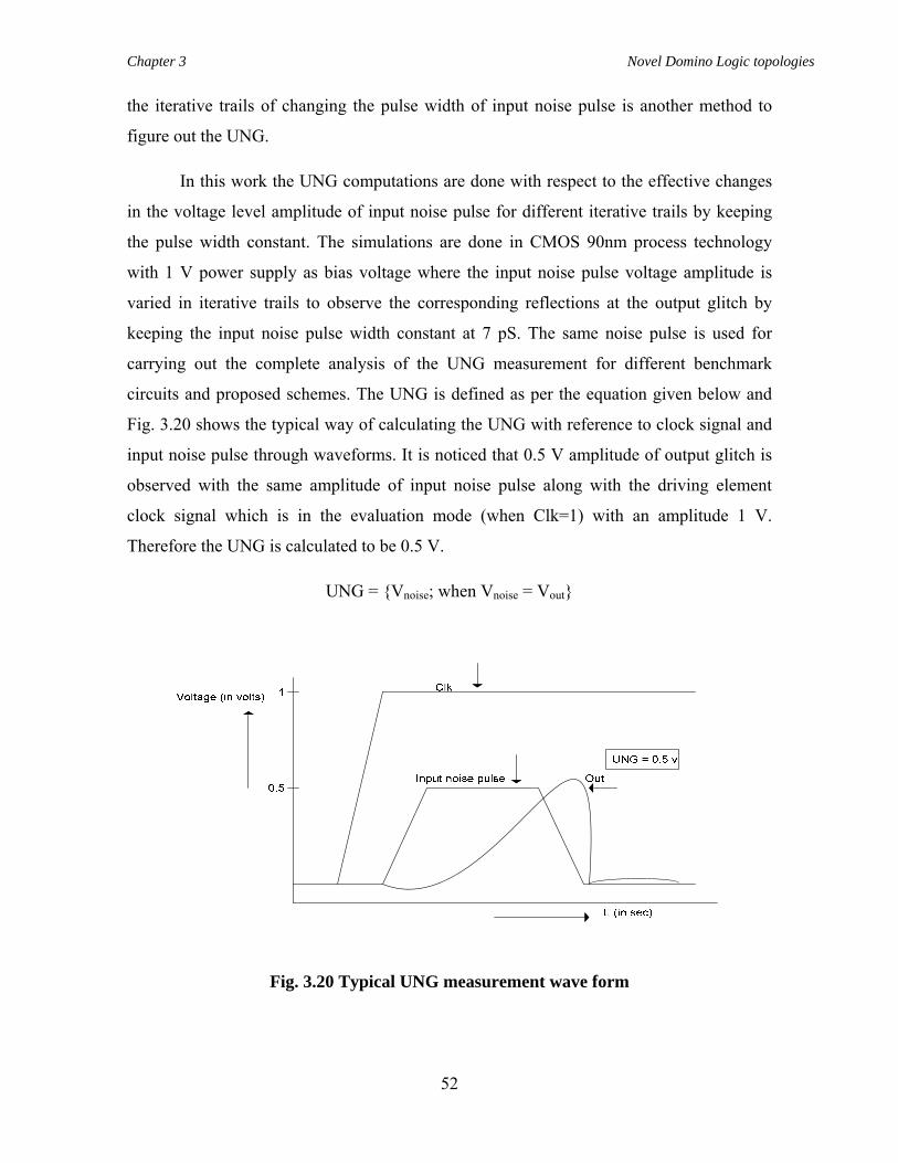
Chapter 3 Novel Domino Logic topologies
52
the iterative trails of changing the pulse width of input noise pulse is another method to
figure out the UNG.
In this work the UNG computations are done with respect to the effective changes
in the voltage level amplitude of input noise pulse for different iterative trails by keeping
the pulse width constant. The simulations are done in CMOS 90nm process technology
with 1 V power supply as bias voltage where the input noise pulse voltage amplitude is
varied in iterative trails to observe the corresponding reflections at the output glitch by
keeping the input noise pulse width constant at 7 pS. The same noise pulse is used for
carrying out the complete analysis of the UNG measurement for different benchmark
circuits and proposed schemes. The UNG is defined as per the equation given below and
Fig. 3.20 shows the typical way of calculating the UNG with reference to clock signal and
input noise pulse through waveforms. It is noticed that 0.5 V amplitude of output glitch is
observed with the same amplitude of input noise pulse along with the driving element
clock signal which is in the evaluation mode (when Clk=1) with an amplitude 1 V.
Therefore the UNG is calculated to be 0.5 V.
UNG = {Vnoise; when Vnoise = Vout}
Fig. 3.20 Typical UNG measurement wave form
Chapter 3 Novel Domino Logic topologies
53
Noise and leakage issues in domino logic circuits
Noise is dominant parameter for the analysis of any digital logic circuit at different
ambient conditions where the functionality may vary depending on the application and
design requirement. Noise in digital circuits has got its own significant role to govern the
functionality of the particular design altogether. There are different sources of noise in
deep submicron regime. Dynamic logic assures high performance when compared to static
counterpart circuits. But there are few significant parametric considerations that must be
taken into account for proper functioning of clocked logic circuits. These issues are
referred as signal integrity issues which are mentioned here but detailed explanation with
complete analysis is given in the next chapter. They are
(1) Crosstalk,
(2) Charge leakage currents,
(3) Charge sharing,
(4) Capacitive coupling,
(5) Clock feed through and
(6) Small variations of nominal supply voltage.
3.4 Process Corner analysis In the process of semiconductor manufacturing industry, the process corner analysis,
which plays a vital role as an effective technique for Design of Experiments (DoE), refers
to random variations of physical fabrication parameters exploited in employing the design
of an Integrated Circuit (IC) to a silicon wafer. The extreme variations in the parameters
which will show their impact on the overall functionality of the design are analyzed by this
process corner analysis within which that particular circuit that is etched onto the wafer is
expected to operate correctly without deviating from its normal functionality. Thus a
fabricated design being tested at these various process corners may run slower or faster
than specified speed of operation but if it does not operate at all at any of these conditional
variations or corners, then the circuit design is considered to be an inadequate design.
Robustness of any designed digital IC is the primary designing metric parameter which
must be scrutinized thoroughly by the manufacturers of semiconductor industry at different
ambient conditions by subjecting the design to extreme conditional variations like
Chapter 3 Novel Domino Logic topologies
54
threshold voltage, clock frequency, and temperature. This typical phenomenon is called
design characterization that results in getting new observations and solutions which can be
plotted with the help of a graphical technique known as ‘shmoo’ plot with the prior
indication of boundary limitations of the circuit design beyond which the design functions
to fail for a given set of combinational process corner variations at different environmental
conditions.
This, also referred as corner-lot analysis, is the most effective method in digital
electronics as it includes the process of subjecting the design to the extreme conditional
variations directly on the speed of switching activity of transistors which is irrelevant for
normal analog circuits.
In VLSI microprocessor design and semiconductor fabrication, this process corner
analysis constitutes few variations typically five from the normal doping concentrations of
transistors on a silicon wafer which can cause predominant alterations in the operation
through the duty cycle and slew rate of signals of digital circuits and can sometimes lead to
the catastrophic failure of the total system.
Types of corners:
There are two kinds of process corners typically FEL (Front End of Line) and BEL
(Back End of Line) where the former one is normally employed at the schematic design
level and the latter one includes the effect of PVT (Process-Voltage-Temperature)
variations on on-chip interconnections.
FEL corners:
Nomenclature for FEL corners includes two-letter representation where the first
letter refers to NMOS device corner and the second letter is related to PMOS device
corner. So this convention has got 5 typical corners known as NN (Normal-Normal) or TT
(Typical Typical), FF (Fast-Fast), SS (Slow-Slow), FS (Fast-Slow) and SF (Slow-Fast) that
exhibit the mobility of carriers which is greater and lower than the normal specified
conditions respectively. Therefore a corner represented as FS, for example, indicates a fast
NMOS device and a slow PMOS device.
Amongst five corners, the first three corners (NN, FF and SS) are known as even corners
since both the types of devices are evenly or simultaneously affected and do not adversely
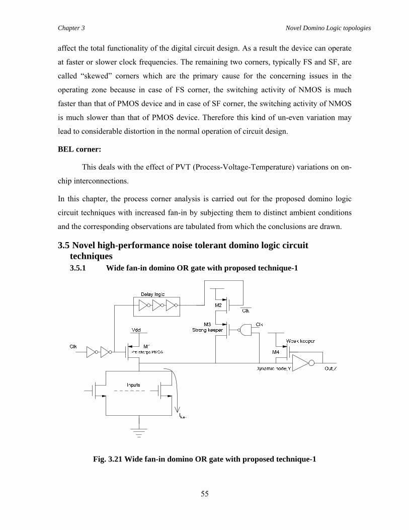
Chapter 3 Novel Domino Logic topologies
55
affect the total functionality of the digital circuit design. As a result the device can operate
at faster or slower clock frequencies. The remaining two corners, typically FS and SF, are
called “skewed” corners which are the primary cause for the concerning issues in the
operating zone because in case of FS corner, the switching activity of NMOS is much
faster than that of PMOS device and in case of SF corner, the switching activity of NMOS
is much slower than that of PMOS device. Therefore this kind of un-even variation may
lead to considerable distortion in the normal operation of circuit design.
BEL corner:
This deals with the effect of PVT (Process-Voltage-Temperature) variations on on-
chip interconnections.
In this chapter, the process corner analysis is carried out for the proposed domino logic
circuit techniques with increased fan-in by subjecting them to distinct ambient conditions
and the corresponding observations are tabulated from which the conclusions are drawn.
3.5 Novel high-performance noise tolerant domino logic circuit techniques 3.5.1 Wide fan-in domino OR gate with proposed technique-1
Fig. 3.21 Wide fan-in domino OR gate with proposed technique-1
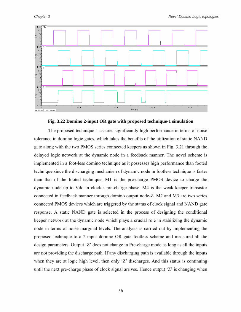
Chapter 3 Novel Domino Logic topologies
56
Fig. 3.22 Domino 2-input OR gate with proposed technique-1 simulation
The proposed technique-1 assures significantly high performance in terms of noise
tolerance in domino logic gates, which takes the benefits of the utilization of static NAND
gate along with the two PMOS series connected keepers as shown in Fig. 3.21 through the
delayed logic network at the dynamic node in a feedback manner. The novel scheme is
implemented in a foot-less domino technique as it possesses high performance than footed
technique since the discharging mechanism of dynamic node in footless technique is faster
than that of the footed technique. M1 is the pre-charge PMOS device to charge the
dynamic node up to Vdd in clock’s pre-charge phase. M4 is the weak keeper transistor
connected in feedback manner through domino output node-Z. M2 and M3 are two series
connected PMOS devices which are triggered by the status of clock signal and NAND gate
response. A static NAND gate is selected in the process of designing the conditional
keeper network at the dynamic node which plays a crucial role in stabilizing the dynamic
node in terms of noise marginal levels. The analysis is carried out by implementing the
proposed technique to a 2-input domino OR gate footless scheme and measured all the
design parameters. Output ‘Z’ does not change in Pre-charge mode as long as all the inputs
are not providing the discharge path. If any discharging path is available through the inputs
when they are at logic high level, then only ‘Z’ discharges. And this status is continuing
until the next pre-charge phase of clock signal arrives. Hence output ‘Z’ is changing when
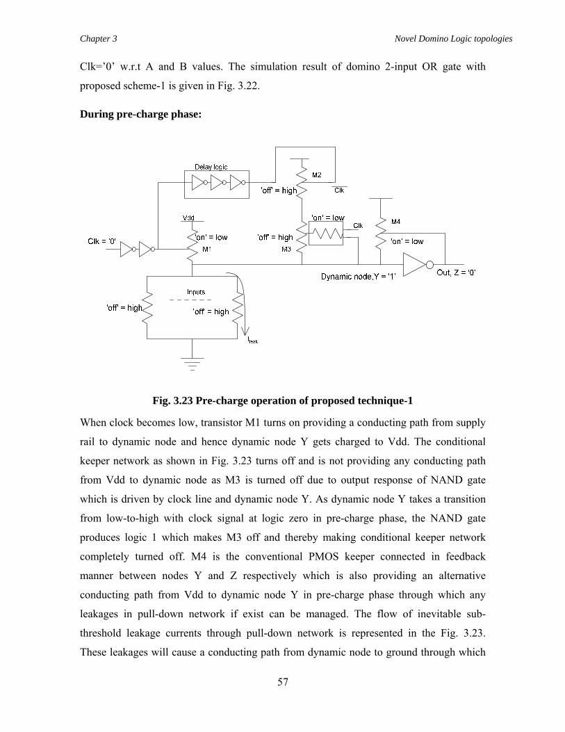
Chapter 3 Novel Domino Logic topologies
57
Clk=’0’ w.r.t A and B values. The simulation result of domino 2-input OR gate with
proposed scheme-1 is given in Fig. 3.22.
During pre-charge phase:
Fig. 3.23 Pre-charge operation of proposed technique-1
When clock becomes low, transistor M1 turns on providing a conducting path from supply
rail to dynamic node and hence dynamic node Y gets charged to Vdd. The conditional
keeper network as shown in Fig. 3.23 turns off and is not providing any conducting path
from Vdd to dynamic node as M3 is turned off due to output response of NAND gate
which is driven by clock line and dynamic node Y. As dynamic node Y takes a transition
from low-to-high with clock signal at logic zero in pre-charge phase, the NAND gate
produces logic 1 which makes M3 off and thereby making conditional keeper network
completely turned off. M4 is the conventional PMOS keeper connected in feedback
manner between nodes Y and Z respectively which is also providing an alternative
conducting path from Vdd to dynamic node Y in pre-charge phase through which any
leakages in pull-down network if exist can be managed. The flow of inevitable sub-
threshold leakage currents through pull-down network is represented in the Fig. 3.23.
These leakages will cause a conducting path from dynamic node to ground through which
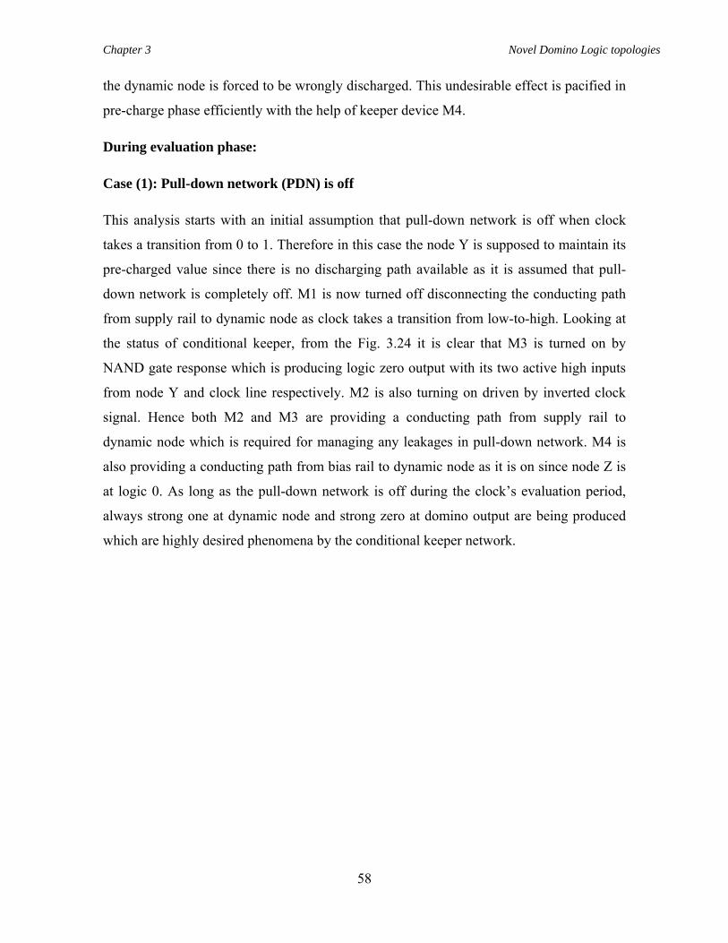
Chapter 3 Novel Domino Logic topologies
58
the dynamic node is forced to be wrongly discharged. This undesirable effect is pacified in
pre-charge phase efficiently with the help of keeper device M4.
During evaluation phase:
Case (1): Pull-down network (PDN) is off
This analysis starts with an initial assumption that pull-down network is off when clock
takes a transition from 0 to 1. Therefore in this case the node Y is supposed to maintain its
pre-charged value since there is no discharging path available as it is assumed that pull-
down network is completely off. M1 is now turned off disconnecting the conducting path
from supply rail to dynamic node as clock takes a transition from low-to-high. Looking at
the status of conditional keeper, from the Fig. 3.24 it is clear that M3 is turned on by
NAND gate response which is producing logic zero output with its two active high inputs
from node Y and clock line respectively. M2 is also turning on driven by inverted clock
signal. Hence both M2 and M3 are providing a conducting path from supply rail to
dynamic node which is required for managing any leakages in pull-down network. M4 is
also providing a conducting path from bias rail to dynamic node as it is on since node Z is
at logic 0. As long as the pull-down network is off during the clock’s evaluation period,
always strong one at dynamic node and strong zero at domino output are being produced
which are highly desired phenomena by the conditional keeper network.
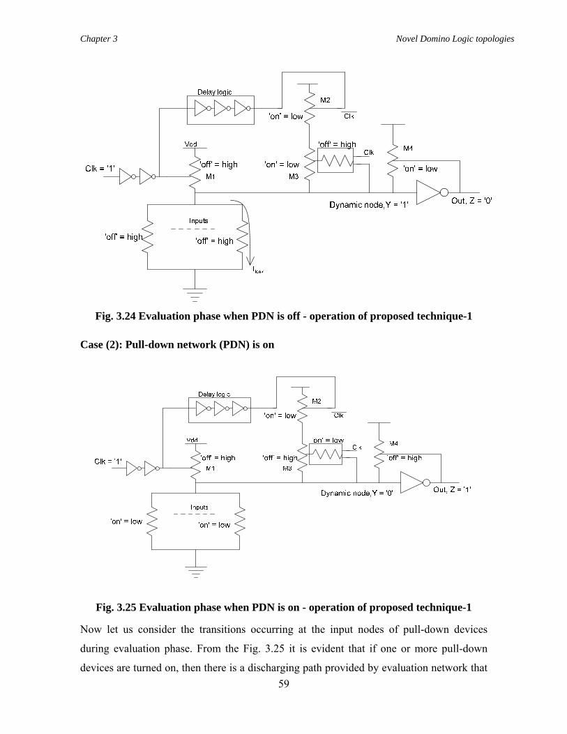
Chapter 3 Novel Domino Logic topologies
59
Fig. 3.24 Evaluation phase when PDN is off - operation of proposed technique-1
Case (2): Pull-down network (PDN) is on
Fig. 3.25 Evaluation phase when PDN is on - operation of proposed technique-1
Now let us consider the transitions occurring at the input nodes of pull-down devices
during evaluation phase. From the Fig. 3.25 it is evident that if one or more pull-down
devices are turned on, then there is a discharging path provided by evaluation network that
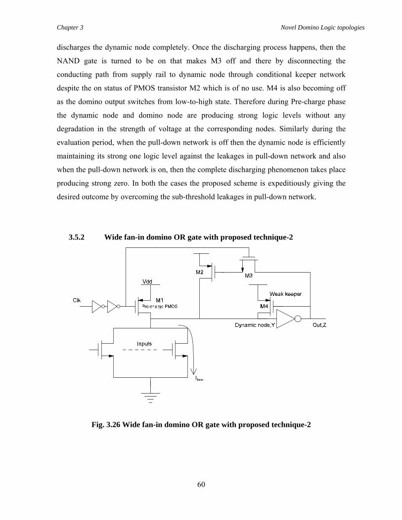
Chapter 3 Novel Domino Logic topologies
60
discharges the dynamic node completely. Once the discharging process happens, then the
NAND gate is turned to be on that makes M3 off and there by disconnecting the
conducting path from supply rail to dynamic node through conditional keeper network
despite the on status of PMOS transistor M2 which is of no use. M4 is also becoming off
as the domino output switches from low-to-high state. Therefore during Pre-charge phase
the dynamic node and domino node are producing strong logic levels without any
degradation in the strength of voltage at the corresponding nodes. Similarly during the
evaluation period, when the pull-down network is off then the dynamic node is efficiently
maintaining its strong one logic level against the leakages in pull-down network and also
when the pull-down network is on, then the complete discharging phenomenon takes place
producing strong zero. In both the cases the proposed scheme is expeditiously giving the
desired outcome by overcoming the sub-threshold leakages in pull-down network.
3.5.2 Wide fan-in domino OR gate with proposed technique-2
Fig. 3.26 Wide fan-in domino OR gate with proposed technique-2
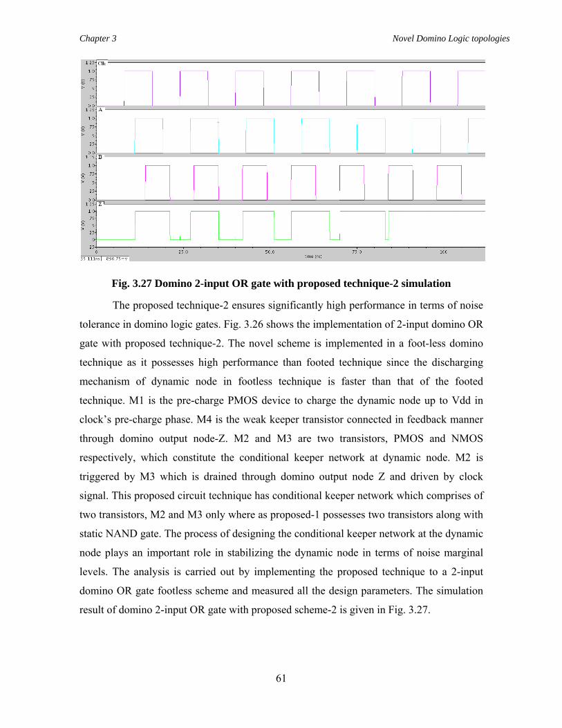
Chapter 3 Novel Domino Logic topologies
61
Fig. 3.27 Domino 2-input OR gate with proposed technique-2 simulation
The proposed technique-2 ensures significantly high performance in terms of noise
tolerance in domino logic gates. Fig. 3.26 shows the implementation of 2-input domino OR
gate with proposed technique-2. The novel scheme is implemented in a foot-less domino
technique as it possesses high performance than footed technique since the discharging
mechanism of dynamic node in footless technique is faster than that of the footed
technique. M1 is the pre-charge PMOS device to charge the dynamic node up to Vdd in
clock’s pre-charge phase. M4 is the weak keeper transistor connected in feedback manner
through domino output node-Z. M2 and M3 are two transistors, PMOS and NMOS
respectively, which constitute the conditional keeper network at dynamic node. M2 is
triggered by M3 which is drained through domino output node Z and driven by clock
signal. This proposed circuit technique has conditional keeper network which comprises of
two transistors, M2 and M3 only where as proposed-1 possesses two transistors along with
static NAND gate. The process of designing the conditional keeper network at the dynamic
node plays an important role in stabilizing the dynamic node in terms of noise marginal
levels. The analysis is carried out by implementing the proposed technique to a 2-input
domino OR gate footless scheme and measured all the design parameters. The simulation
result of domino 2-input OR gate with proposed scheme-2 is given in Fig. 3.27.
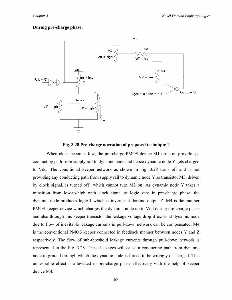
Chapter 3 Novel Domino Logic topologies
62
During pre-charge phase:
Fig. 3.28 Pre-charge operation of proposed technique-2
When clock becomes low, the pre-charge PMOS device M1 turns on providing a
conducting path from supply rail to dynamic node and hence dynamic node Y gets charged
to Vdd. The conditional keeper network as shown in Fig. 3.28 turns off and is not
providing any conducting path from supply rail to dynamic node Y as transistor M3, driven
by clock signal, is turned off which cannot turn M2 on. As dynamic node Y takes a
transition from low-to-high with clock signal at logic zero in pre-charge phase, the
dynamic node produces logic 1 which is inverter at domino output Z. M4 is the another
PMOS keeper device which charges the dynamic node up to Vdd during pre-charge phase
and also through this keeper transistor the leakage voltage drop if exists at dynamic node
due to flow of inevitable leakage currents in pull-down network can be compensated. M4
is the conventional PMOS keeper connected in feedback manner between nodes Y and Z
respectively. The flow of sub-threshold leakage currents through pull-down network is
represented in the Fig. 3.28. These leakages will cause a conducting path from dynamic
node to ground through which the dynamic node is forced to be wrongly discharged. This
undesirable effect is alleviated in pre-charge phase effectively with the help of keeper
device M4.
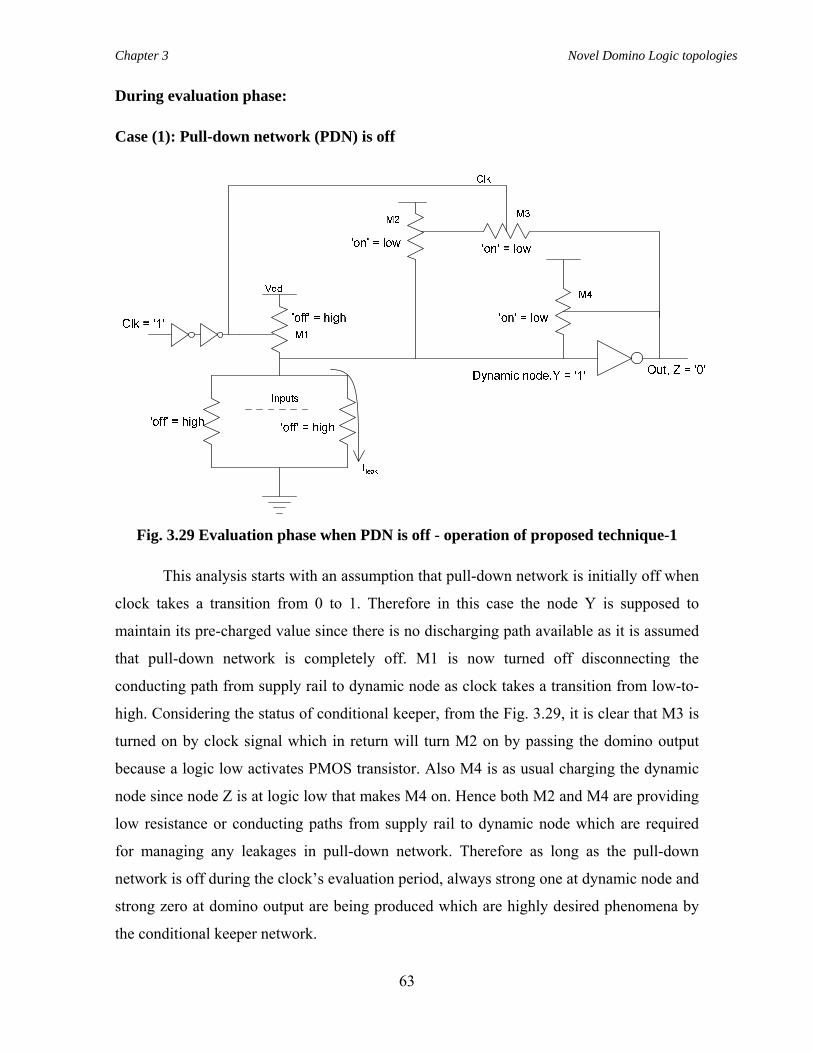
Chapter 3 Novel Domino Logic topologies
63
During evaluation phase:
Case (1): Pull-down network (PDN) is off
Fig. 3.29 Evaluation phase when PDN is off - operation of proposed technique-1
This analysis starts with an assumption that pull-down network is initially off when
clock takes a transition from 0 to 1. Therefore in this case the node Y is supposed to
maintain its pre-charged value since there is no discharging path available as it is assumed
that pull-down network is completely off. M1 is now turned off disconnecting the
conducting path from supply rail to dynamic node as clock takes a transition from low-to-
high. Considering the status of conditional keeper, from the Fig. 3.29, it is clear that M3 is
turned on by clock signal which in return will turn M2 on by passing the domino output
because a logic low activates PMOS transistor. Also M4 is as usual charging the dynamic
node since node Z is at logic low that makes M4 on. Hence both M2 and M4 are providing
low resistance or conducting paths from supply rail to dynamic node which are required
for managing any leakages in pull-down network. Therefore as long as the pull-down
network is off during the clock’s evaluation period, always strong one at dynamic node and
strong zero at domino output are being produced which are highly desired phenomena by
the conditional keeper network.

Chapter 3 Novel Domino Logic topologies
64
Case (2): Pull-down network (PDN) is on
Fig. 3.30 Evaluation phase when PDN is on - operation of proposed technique-2
Now let us consider the transitions occurring at the input nodes of pull-down devices
during evaluation phase. From the Fig. 3.30, it is clear that if one or more pull-down
devices are turned on, then there is a discharging path provided by pull-down network that
discharges the dynamic node completely. Once the discharging process takes place, then
the dynamic node is turned to be low which in turn produces a strong one at domino output
that will again result in turning the transistor M4 off. As domino output node Z takes a
transition from low-to-high, this logic one will be passed by the transistor M3, which was
already on, to M2 that results in turning it off. This clearly implies that there exists no low
resistance path or conducting path from bias rail to dynamic node. Therefore during pre-
charge phase of clock signal, the dynamic node and domino node are producing strong
logic levels without any deterioration in the strength of voltage levels at the corresponding
nodes. Similarly during the evaluation period, when the pull-down network is off then the
dynamic node is efficiently maintaining its strong one logic level against the leakages
existing in pull-down network and also when the pull-down network is on, then the
complete discharging phenomenon takes place producing strong zero. In both the cases the
proposed scheme is expeditiously giving the required result by mitigating the impact of the
sub-threshold leakages in pull-down network.
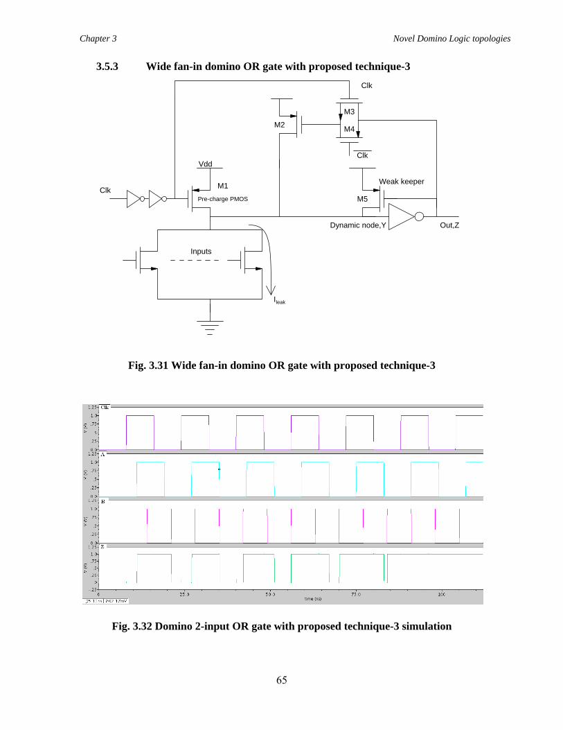
Chapter 3 Novel Domino Logic topologies
65
3.5.3 Wide fan-in domino OR gate with proposed technique-3
Out,Z
Inputs
Ileak
Vdd
Pre-charge PMOSClk
Clk
Clk
Dynamic node,Y
M3
M4M2
M1
M5
Weak keeper
Fig. 3.31 Wide fan-in domino OR gate with proposed technique-3
Fig. 3.32 Domino 2-input OR gate with proposed technique-3 simulation
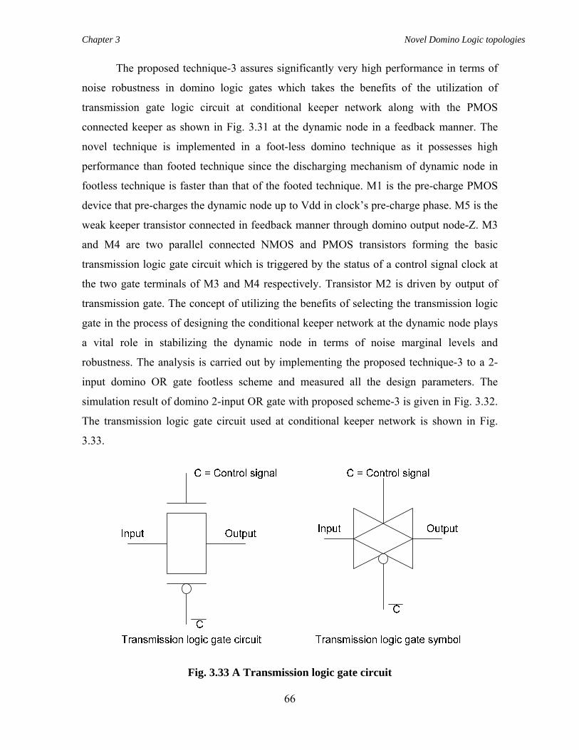
Chapter 3 Novel Domino Logic topologies
66
The proposed technique-3 assures significantly very high performance in terms of
noise robustness in domino logic gates which takes the benefits of the utilization of
transmission gate logic circuit at conditional keeper network along with the PMOS
connected keeper as shown in Fig. 3.31 at the dynamic node in a feedback manner. The
novel technique is implemented in a foot-less domino technique as it possesses high
performance than footed technique since the discharging mechanism of dynamic node in
footless technique is faster than that of the footed technique. M1 is the pre-charge PMOS
device that pre-charges the dynamic node up to Vdd in clock’s pre-charge phase. M5 is the
weak keeper transistor connected in feedback manner through domino output node-Z. M3
and M4 are two parallel connected NMOS and PMOS transistors forming the basic
transmission logic gate circuit which is triggered by the status of a control signal clock at
the two gate terminals of M3 and M4 respectively. Transistor M2 is driven by output of
transmission gate. The concept of utilizing the benefits of selecting the transmission logic
gate in the process of designing the conditional keeper network at the dynamic node plays
a vital role in stabilizing the dynamic node in terms of noise marginal levels and
robustness. The analysis is carried out by implementing the proposed technique-3 to a 2-
input domino OR gate footless scheme and measured all the design parameters. The
simulation result of domino 2-input OR gate with proposed scheme-3 is given in Fig. 3.32.
The transmission logic gate circuit used at conditional keeper network is shown in Fig.
3.33.
Fig. 3.33 A Transmission logic gate circuit
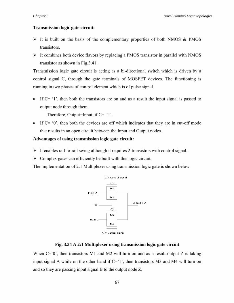
Chapter 3 Novel Domino Logic topologies
67
Transmission logic gate circuit:
It is built on the basis of the complementary properties of both NMOS & PMOS
transistors.
It combines both device flavors by replacing a PMOS transistor in parallel with NMOS
transistor as shown in Fig.3.41.
Transmission logic gate circuit is acting as a bi-directional switch which is driven by a
control signal C, through the gate terminals of MOSFET devices. The functioning is
running in two phases of control element which is of pulse signal.
• If C= ‘1’, then both the transistors are on and as a result the input signal is passed to
output node through them.
Therefore, Output=Input, if C= ‘1’.
• If C= ‘0’, then both the devices are off which indicates that they are in cut-off mode
that results in an open circuit between the Input and Output nodes.
Advantages of using transmission logic gate circuit:
It enables rail-to-rail swing although it requires 2-transistors with control signal.
Complex gates can efficiently be built with this logic circuit.
The implementation of 2:1 Multiplexer using transmission logic gate is shown below.
Fig. 3.34 A 2:1 Multiplexer using transmission logic gate circuit
When C=’0’, then transistors M1 and M2 will turn on and as a result output Z is taking
input signal A while on the other hand if C=’1’, then transistors M3 and M4 will turn on
and so they are passing input signal B to the output node Z.
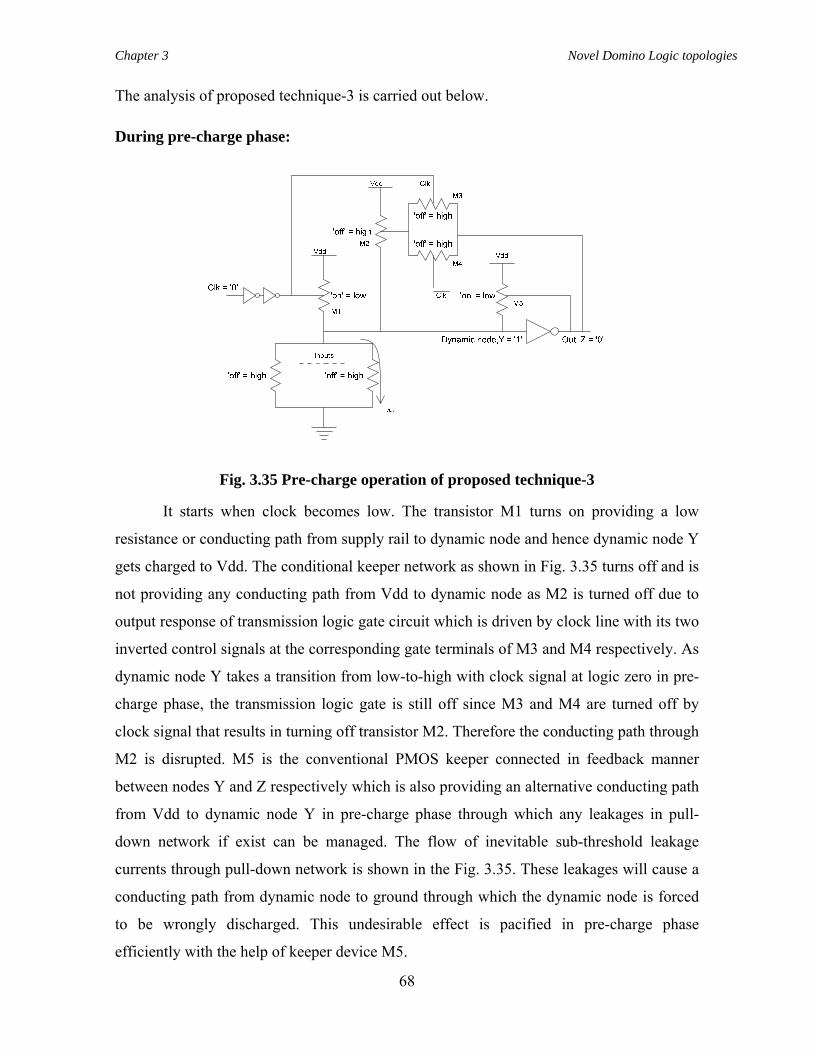
Chapter 3 Novel Domino Logic topologies
68
The analysis of proposed technique-3 is carried out below.
During pre-charge phase:
Fig. 3.35 Pre-charge operation of proposed technique-3
It starts when clock becomes low. The transistor M1 turns on providing a low
resistance or conducting path from supply rail to dynamic node and hence dynamic node Y
gets charged to Vdd. The conditional keeper network as shown in Fig. 3.35 turns off and is
not providing any conducting path from Vdd to dynamic node as M2 is turned off due to
output response of transmission logic gate circuit which is driven by clock line with its two
inverted control signals at the corresponding gate terminals of M3 and M4 respectively. As
dynamic node Y takes a transition from low-to-high with clock signal at logic zero in pre-
charge phase, the transmission logic gate is still off since M3 and M4 are turned off by
clock signal that results in turning off transistor M2. Therefore the conducting path through
M2 is disrupted. M5 is the conventional PMOS keeper connected in feedback manner
between nodes Y and Z respectively which is also providing an alternative conducting path
from Vdd to dynamic node Y in pre-charge phase through which any leakages in pull-
down network if exist can be managed. The flow of inevitable sub-threshold leakage
currents through pull-down network is shown in the Fig. 3.35. These leakages will cause a
conducting path from dynamic node to ground through which the dynamic node is forced
to be wrongly discharged. This undesirable effect is pacified in pre-charge phase
efficiently with the help of keeper device M5.
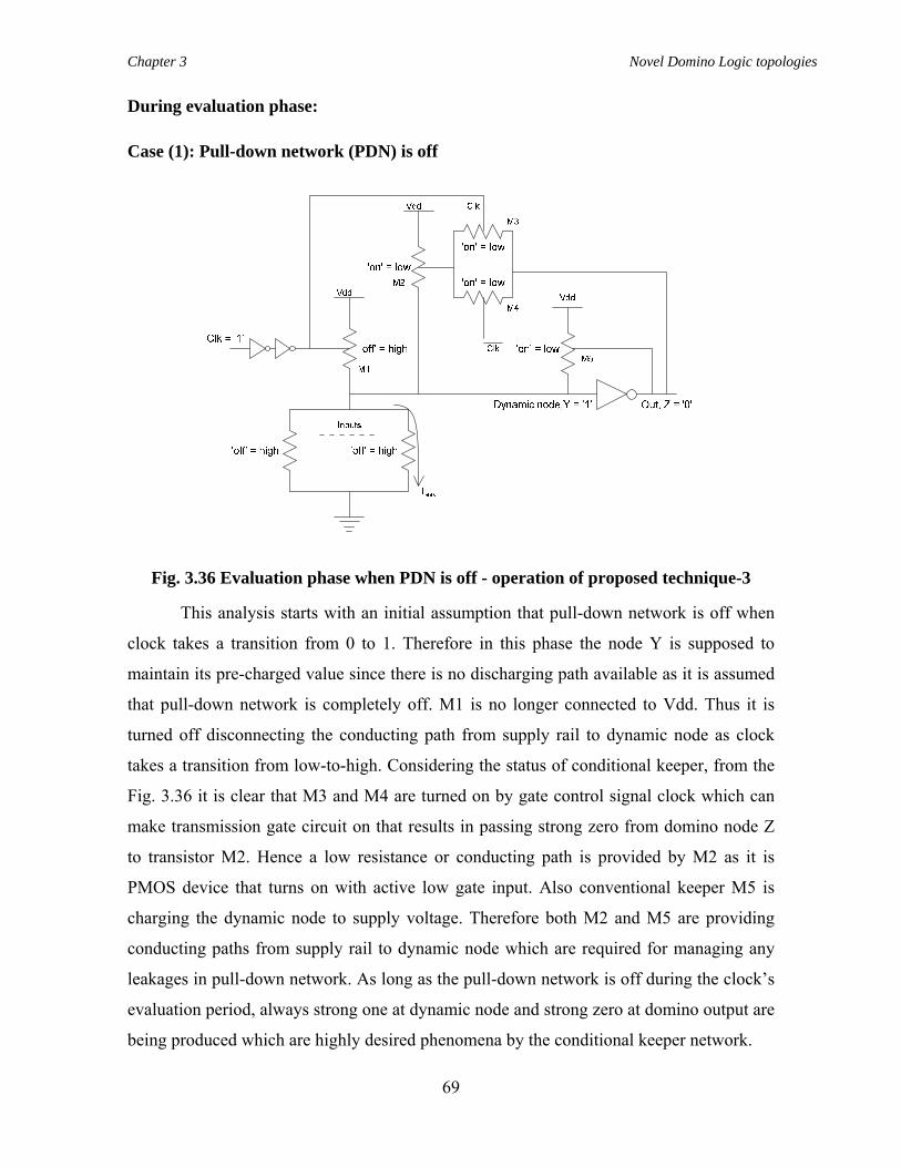
Chapter 3 Novel Domino Logic topologies
69
During evaluation phase:
Case (1): Pull-down network (PDN) is off
Fig. 3.36 Evaluation phase when PDN is off - operation of proposed technique-3
This analysis starts with an initial assumption that pull-down network is off when
clock takes a transition from 0 to 1. Therefore in this phase the node Y is supposed to
maintain its pre-charged value since there is no discharging path available as it is assumed
that pull-down network is completely off. M1 is no longer connected to Vdd. Thus it is
turned off disconnecting the conducting path from supply rail to dynamic node as clock
takes a transition from low-to-high. Considering the status of conditional keeper, from the
Fig. 3.36 it is clear that M3 and M4 are turned on by gate control signal clock which can
make transmission gate circuit on that results in passing strong zero from domino node Z
to transistor M2. Hence a low resistance or conducting path is provided by M2 as it is
PMOS device that turns on with active low gate input. Also conventional keeper M5 is
charging the dynamic node to supply voltage. Therefore both M2 and M5 are providing
conducting paths from supply rail to dynamic node which are required for managing any
leakages in pull-down network. As long as the pull-down network is off during the clock’s
evaluation period, always strong one at dynamic node and strong zero at domino output are
being produced which are highly desired phenomena by the conditional keeper network.
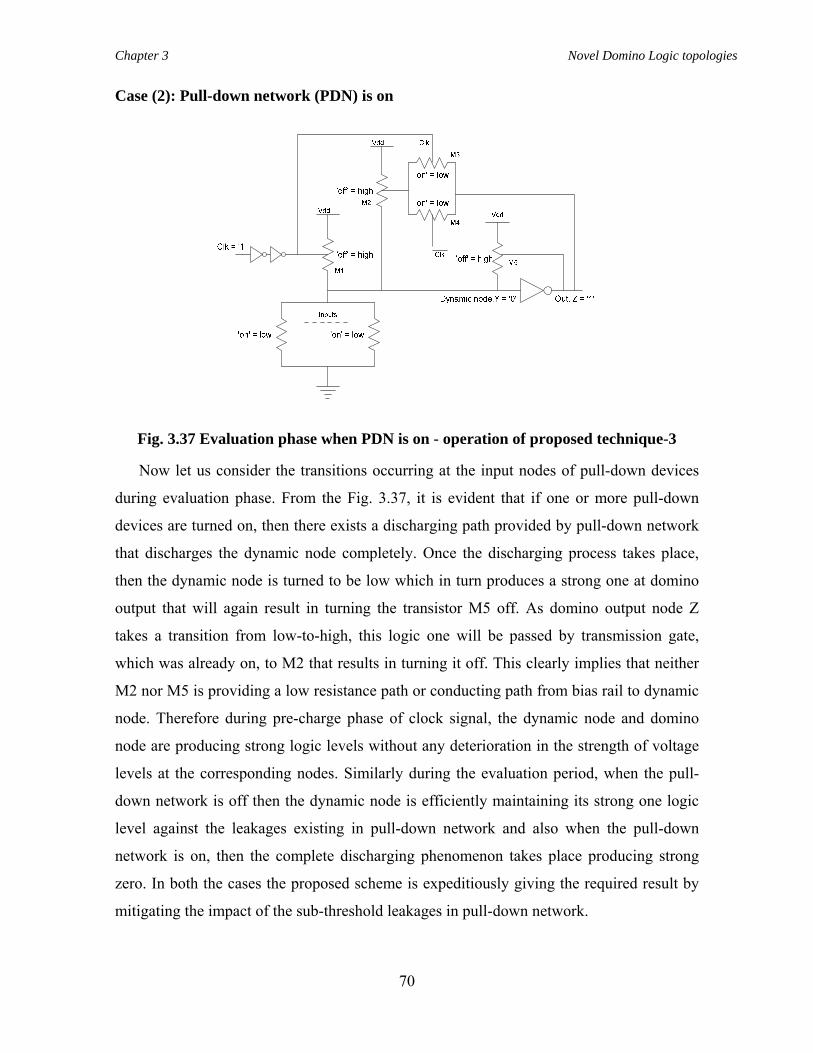
Chapter 3 Novel Domino Logic topologies
70
Case (2): Pull-down network (PDN) is on
Fig. 3.37 Evaluation phase when PDN is on - operation of proposed technique-3
Now let us consider the transitions occurring at the input nodes of pull-down devices
during evaluation phase. From the Fig. 3.37, it is evident that if one or more pull-down
devices are turned on, then there exists a discharging path provided by pull-down network
that discharges the dynamic node completely. Once the discharging process takes place,
then the dynamic node is turned to be low which in turn produces a strong one at domino
output that will again result in turning the transistor M5 off. As domino output node Z
takes a transition from low-to-high, this logic one will be passed by transmission gate,
which was already on, to M2 that results in turning it off. This clearly implies that neither
M2 nor M5 is providing a low resistance path or conducting path from bias rail to dynamic
node. Therefore during pre-charge phase of clock signal, the dynamic node and domino
node are producing strong logic levels without any deterioration in the strength of voltage
levels at the corresponding nodes. Similarly during the evaluation period, when the pull-
down network is off then the dynamic node is efficiently maintaining its strong one logic
level against the leakages existing in pull-down network and also when the pull-down
network is on, then the complete discharging phenomenon takes place producing strong
zero. In both the cases the proposed scheme is expeditiously giving the required result by
mitigating the impact of the sub-threshold leakages in pull-down network.
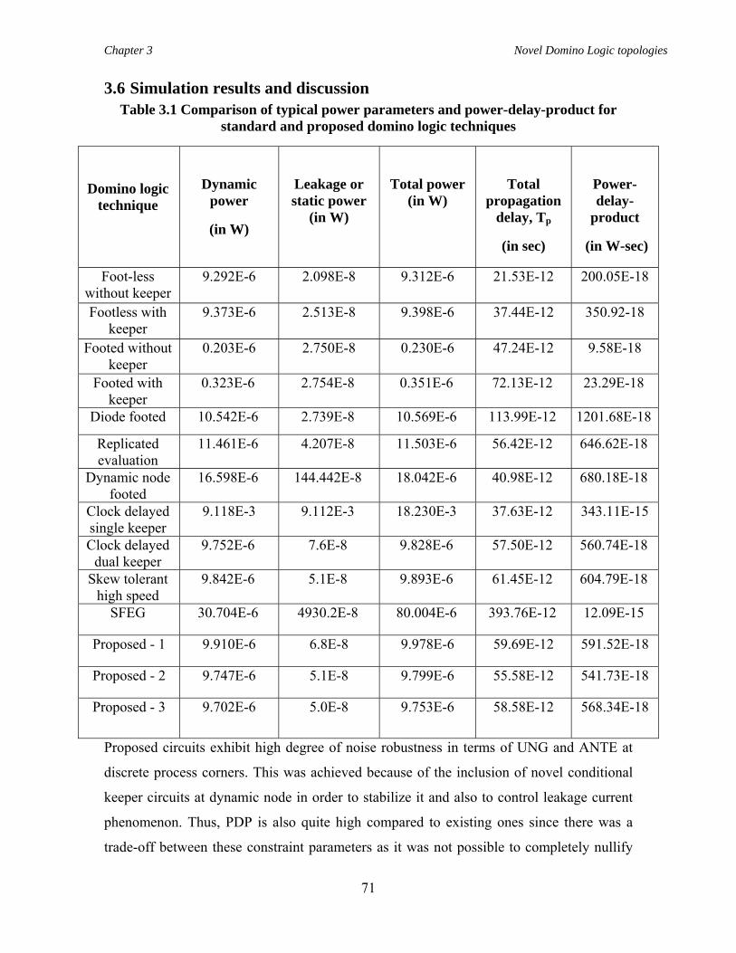
Chapter 3 Novel Domino Logic topologies
71
3.6 Simulation results and discussion Table 3.1 Comparison of typical power parameters and power-delay-product for
standard and proposed domino logic techniques
Domino logic technique
Dynamic power
(in W)
Leakage or static power
(in W)
Total power (in W)
Total propagation
delay, Tp
(in sec)
Power-delay-
product
(in W-sec)
Foot-less without keeper
9.292E-6 2.098E-8 9.312E-6 21.53E-12 200.05E-18
Footless with keeper
9.373E-6 2.513E-8 9.398E-6 37.44E-12 350.92-18
Footed without keeper
0.203E-6 2.750E-8 0.230E-6 47.24E-12 9.58E-18
Footed with keeper
0.323E-6 2.754E-8 0.351E-6 72.13E-12 23.29E-18
Diode footed 10.542E-6 2.739E-8 10.569E-6 113.99E-12 1201.68E-18
Replicated evaluation
11.461E-6 4.207E-8 11.503E-6 56.42E-12 646.62E-18
Dynamic node footed
16.598E-6 144.442E-8 18.042E-6 40.98E-12 680.18E-18
Clock delayed single keeper
9.118E-3 9.112E-3 18.230E-3 37.63E-12 343.11E-15
Clock delayed dual keeper
9.752E-6 7.6E-8 9.828E-6 57.50E-12 560.74E-18
Skew tolerant high speed
9.842E-6 5.1E-8 9.893E-6 61.45E-12 604.79E-18
SFEG 30.704E-6 4930.2E-8 80.004E-6 393.76E-12 12.09E-15
Proposed - 1 9.910E-6 6.8E-8 9.978E-6 59.69E-12 591.52E-18
Proposed - 2 9.747E-6 5.1E-8 9.799E-6 55.58E-12 541.73E-18
Proposed - 3 9.702E-6 5.0E-8 9.753E-6 58.58E-12 568.34E-18
Proposed circuits exhibit high degree of noise robustness in terms of UNG and ANTE at
discrete process corners. This was achieved because of the inclusion of novel conditional
keeper circuits at dynamic node in order to stabilize it and also to control leakage current
phenomenon. Thus, PDP is also quite high compared to existing ones since there was a
trade-off between these constraint parameters as it was not possible to completely nullify
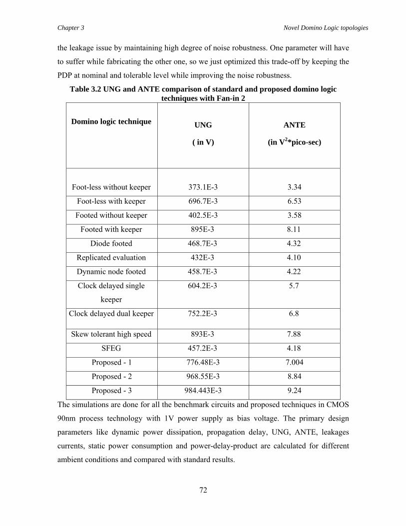
Chapter 3 Novel Domino Logic topologies
72
the leakage issue by maintaining high degree of noise robustness. One parameter will have
to suffer while fabricating the other one, so we just optimized this trade-off by keeping the
PDP at nominal and tolerable level while improving the noise robustness.
Table 3.2 UNG and ANTE comparison of standard and proposed domino logic techniques with Fan-in 2
Domino logic technique
UNG
( in V)
ANTE
(in V2*pico-sec)
Foot-less without keeper
373.1E-3
3.34
Foot-less with keeper 696.7E-3 6.53
Footed without keeper 402.5E-3 3.58
Footed with keeper 895E-3 8.11
Diode footed 468.7E-3 4.32
Replicated evaluation 432E-3 4.10
Dynamic node footed 458.7E-3 4.22
Clock delayed single
keeper
604.2E-3 5.7
Clock delayed dual keeper 752.2E-3 6.8
Skew tolerant high speed 893E-3 7.88
SFEG 457.2E-3 4.18
Proposed - 1 776.48E-3 7.004
Proposed - 2 968.55E-3 8.84
Proposed - 3 984.443E-3 9.24
The simulations are done for all the benchmark circuits and proposed techniques in CMOS
90nm process technology with 1V power supply as bias voltage. The primary design
parameters like dynamic power dissipation, propagation delay, UNG, ANTE, leakages
currents, static power consumption and power-delay-product are calculated for different
ambient conditions and compared with standard results.
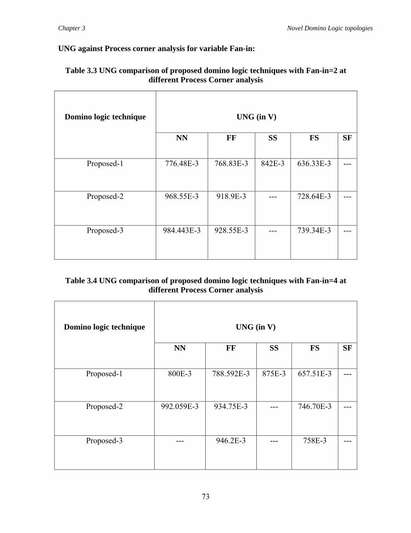
Chapter 3 Novel Domino Logic topologies
73
UNG against Process corner analysis for variable Fan-in:
Table 3.3 UNG comparison of proposed domino logic techniques with Fan-in=2 at different Process Corner analysis
Domino logic technique
UNG (in V)
NN FF SS FS SF
Proposed-1 776.48E-3 768.83E-3 842E-3 636.33E-3 ---
Proposed-2 968.55E-3 918.9E-3 --- 728.64E-3 ---
Proposed-3 984.443E-3 928.55E-3 --- 739.34E-3 ---
Table 3.4 UNG comparison of proposed domino logic techniques with Fan-in=4 at different Process Corner analysis
Domino logic technique
UNG (in V)
NN FF SS FS SF
Proposed-1 800E-3 788.592E-3 875E-3 657.51E-3 ---
Proposed-2 992.059E-3 934.75E-3 --- 746.70E-3 ---
Proposed-3 --- 946.2E-3 --- 758E-3 ---

Chapter 3 Novel Domino Logic topologies
74
Table 3.5 UNG comparison of proposed domino logic techniques with Fan-in=8 at different Process Corner analysis
Domino logic technique
UNG (in V)
NN FF SS FS SF
Proposed-1 845E-3 828.5E-3 952E-3 697.53E-3 ---
Proposed-2 --- 965.33E-3 --- 782.555E-3 ---
Proposed-3 --- 976E-3 --- 794E-3 ---
Table 3.6 UNG comparison of proposed domino logic techniques with Fan-in=16 at different Process Corner analysis
Domino logic
technique
UNG (in V)
NN FF SS FS SF
Proposed-1 941E-3 910.3E-3 --- 775E-3 ---
Proposed-2 --- --- --- 849.82E-
3
---
Proposed-3 --- --- --- 863E-3 ---
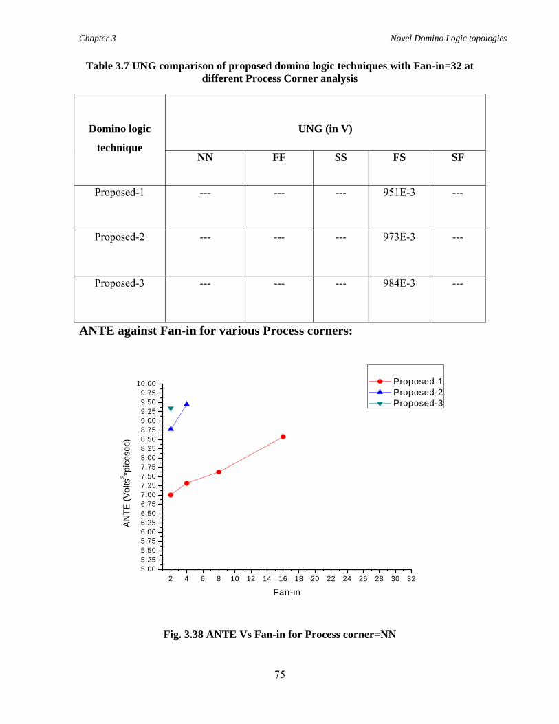
Chapter 3 Novel Domino Logic topologies
75
Table 3.7 UNG comparison of proposed domino logic techniques with Fan-in=32 at different Process Corner analysis
Domino logic
technique
UNG (in V)
NN FF SS FS SF
Proposed-1 --- --- --- 951E-3 ---
Proposed-2 --- --- --- 973E-3 ---
Proposed-3 --- --- --- 984E-3 ---
ANTE against Fan-in for various Process corners:
2 4 6 8 10 12 14 16 18 20 22 24 26 28 30 325.005.255.505.756.006.256.506.757.007.257.507.758.008.258.508.759.009.259.509.75
10.00
AN
TE (V
olts
2 *pic
osec
)
Fan-in
Proposed-1 Proposed-2 Proposed-3
Fig. 3.38 ANTE Vs Fan-in for Process corner=NN
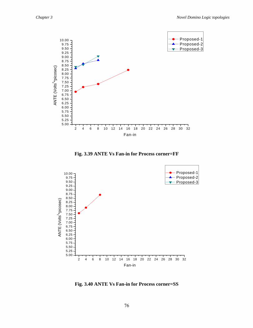
Chapter 3 Novel Domino Logic topologies
76
2 4 6 8 10 12 14 16 18 20 22 24 26 28 30 325.005.255.505.756.006.256.506.757.007.257.507.758.008.258.508.759.009.259.509.75
10.00
AN
TE (V
olts
2 *pic
osec
)
Fan-in
Proposed-1 Proposed-2 Proposed-3
Fig. 3.39 ANTE Vs Fan-in for Process corner=FF
2 4 6 8 10 12 14 16 18 20 22 24 26 28 30 325.005.255.505.756.006.256.506.757.007.257.507.758.008.258.508.759.009.259.509.75
10.00
ANTE
(Vol
ts2 *p
icos
ec)
Fan-in
Proposed-1 Proposed-2 Proposed-3
Fig. 3.40 ANTE Vs Fan-in for Process corner=SS
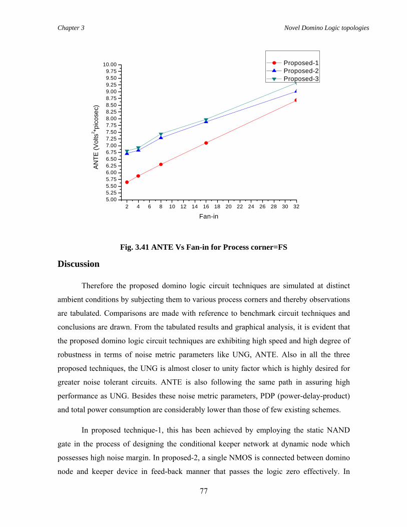
Chapter 3 Novel Domino Logic topologies
77
2 4 6 8 10 12 14 16 18 20 22 24 26 28 30 325.005.255.505.756.006.256.506.757.007.257.507.758.008.258.508.759.009.259.509.75
10.00
AN
TE (V
olts
2 *pic
osec
)
Fan-in
Proposed-1 Proposed-2 Proposed-3
Fig. 3.41 ANTE Vs Fan-in for Process corner=FS
Discussion
Therefore the proposed domino logic circuit techniques are simulated at distinct
ambient conditions by subjecting them to various process corners and thereby observations
are tabulated. Comparisons are made with reference to benchmark circuit techniques and
conclusions are drawn. From the tabulated results and graphical analysis, it is evident that
the proposed domino logic circuit techniques are exhibiting high speed and high degree of
robustness in terms of noise metric parameters like UNG, ANTE. Also in all the three
proposed techniques, the UNG is almost closer to unity factor which is highly desired for
greater noise tolerant circuits. ANTE is also following the same path in assuring high
performance as UNG. Besides these noise metric parameters, PDP (power-delay-product)
and total power consumption are considerably lower than those of few existing schemes.
In proposed technique-1, this has been achieved by employing the static NAND
gate in the process of designing the conditional keeper network at dynamic node which
possesses high noise margin. In proposed-2, a single NMOS is connected between domino
node and keeper device in feed-back manner that passes the logic zero effectively. In
Chapter 3 Novel Domino Logic topologies
78
proposed-3 the transmission gate is adopted in conditional keeper network which stabilizes
the dynamic node from leakages efficaciously, by passing both strong one and strong zero
since it is a mixer of both NMOS and PMOS flavors.
Having analyzed the results from process corner analysis, it is clear that proposed
circuit techniques assure high noise robustness with increased fan-in. There are limitations
too for the functionality of proposed domino logic circuit techniques at various corners.
Proposed techniques are functioning efficiently, at all the corners for lower fan-in circuits
but with increased fan-in, the operating region of design has started becoming limited to
few corners only which might be due to the reason that the circuits are being operated at
lower bias supply voltage around 1 V. Thus increasing the bias voltage range would
facilitate broadening the operating region of proposed domino techniques at all the process
corners for wide fan-in circuits but while doing so the power consumption must be taken
care off as it is directly proportional to square of supply voltage. Hence optimization
through trade-off between supply voltage and process corners is necessary while
improving the proposed domino logic circuit techniques.
Table 3.1 shows the comparison of typical power parameters such as dynamic
power, static power, propagation delay, and power-delay-product for standard and
proposed domino logic techniques. It is evident that the total power consumption and PDP
of proposed circuits are considerably lowered when compared with benchmark circuits.
Table 3.2 gives comparison of UNG and ANTE for standard and proposed domino logic
techniques with fan-in 2 and it is clear that proposed circuits possess improved UNG and
ANTE values.
Looking at the process-corner analysis, amongst five typical corners (NN, SS, FF,
FS and SF), Normal-Normal corner is providing nominal switching threshold voltages for
NMOS and PMOS devices as specified by EDA tool. In general, all the designed circuits
will operate as per design specifications and according to user constraints at NN corner.
Thus evaluation and estimation of overall performance of designed circuit by subjecting at
NN process corner alone does not finish the task. In fact the circuit is required to be tested
by subjecting at all the extreme corners. Having done that entire task, then only the
performance of circuit can be judged. Always the SS corner is assuring increased noise
Chapter 3 Novel Domino Logic topologies
79
tolerance and which is also observed from tabulations. Highest UNG is recorded in SS
corner since both NMOS and PMOS transistors are slow running devices which implied
that their switching threshold voltages are high. Thus, the circuit is made less sensitive to
noise glitches by these SS corner devices and hence the nature of being responsive to gate
input noise glitches is gradually reducing, that in turn increases UNG. So, in comparison
with other process corners, SS corner always exhibits highest UNG. Also in SF corner, as
NMOS switching threshold voltage is higher and PMOS switching threshold voltage is
lower, it also contributes increment in noise gain but not as efficient as SS corner because
the PMOS threshold voltage is responding to noise impulses at gate inputs which makes
the circuit more sensitive to noise glitches. Normally, in comparison with NN, FS and FF
corners, circuit at SF corner exhibits better immunity towards noise. Having analyzed the
proposed circuits at all the extreme corners, SF corner is not at all giving the response.
This is because of the design of conditional keeper circuit which is suitable for high speed
applications. Thus SF corner, which runs with slow NMOS and fast PMOS devices, is not
suitable for proposed circuits. At FF process corner, both NMOS and PMOS devices are of
very high speed with reduced switching threshold voltages and consume more power. Thus
normal circuits usually become more sensitive to noise glitches at gate inputs due to their
lower threshold voltages and as a result UNG is reduced. With increased fan-in, the UNG
in other process corners is gradually lowering since more voltage is required to turn pull-
down network on and discharging phenomenon is becoming slow. But proposed circuits
are functioning at FF corner efficiently as they are designed for high speed applications.
Normally, with increased fan-in, the UNG lowers but the proposed circuit techniques
exhibit the greater noise robustness for wide fan-in also which made them suitable for high
speed applications. The performance of circuit at FS process corner lies in between the
corresponding performances at NN and FF corners. As NMOS possesses lower threshold
voltage, it becomes more sensitive to noise. Despite slow PMOS device, the corner is
lowering the noise immunity. From the tabulations, it is evident that proposed techniques
exhibit high degree of robustness at FS corner too.
Having analyzed the results from process corner analysis, it is clear that proposed
circuit techniques assure high noise robustness with increased fan-in despite few
limitations at various corners. Proposed techniques are functioning efficiently, at all the
Chapter 3 Novel Domino Logic topologies
80
corners for lower fan-in circuits but with increased fan-in, the operating region of design
has started becoming limited to few corners only which might be due to the reason that the
circuits are being operated at lower bias voltage around 1 V. For example, from the
simulations, it is clear that the UNG is getting limited at NN, FF and FS process corners
for higher fan-in. Thus increasing the bias voltage range would facilitate broadening the
operating region of proposed domino techniques at all the process corners for wide fan-in
circuits but while doing so the power consumption must be taken care off as it is directly
proportional to square of supply voltage. Hence optimization through trade-off between
supply voltage and process corners is necessary while improving the proposed domino
logic circuit techniques.
Therefore, the proposed circuits are designed for high speed applications with
greater noise immunity. This is investigated from the tabulations of the analysis of UNG
against process corner analysis for various fan-in circuits. Normally process corners SS
and SF assure higher noise tolerance than FF and FS corners at which the circuits are
becoming more sensitive and vulnerable to noise glitches. But in this chapter the proposed
circuit techniques are exhibiting significantly improved noise tolerance even at FF and FS
corners also. This is because of the design of conditional keeper network particularly the
proposed-3 technique shows greater noise robustness than proposed-1 and proposed-2,
since transmission gate is chosen at keeper network which passes both strong one and
strong zero efficiently and stabilizes the leakages in pull-down network. Improved average
noise threshold energy (ANTE) can also be observed from tabulations.
3.7 Conclusion Therefore this chapter in section-1 gave general introduction to domino logic family.
Section-3.2 discussed standard benchmark domino logic circuit schemes followed
by the analysis of their functionality with simulation results.
In section-3.3, the novel domino logic circuit techniques are proposed and analyzed
their functionality in detail with equivalent circuit diagrams in all operating regions along
with simulation results.
Chapter 3 Novel Domino Logic topologies
81
In section-3.4, the noise analysis is carried out which includes the need for
robustness, various metric parameters for measuring noise immunity or robustness of
domino circuits such as UNG, ANTE along with the method of calculations, various
sources of noise in domino logic circuits and their role on operating region.
Section-3.5 gives the description of process corner analysis and various corners
involved in it along with their significant role on the overall functionality of the designed
domino logic circuit. Also the consequences of subjecting the device to the extreme
corners with the boundary limitations are discussed.
Section-3.6 is the result section which showed the calculations and comparisons of
all the parameters of standard benchmark circuits and proposed domino techniques. The
primary design parameters such dynamic power, leakage or static power, total power, PDP
(power-delay-product), UNG and ANTE for various fan-in circuits of existing and
proposed techniques are measured. The comparisons along with graphical analysis are
made and discussed the functionality with pros and cons.
The highest UNG of 984.4E-3 V and ANTE of 9.45E-12 V-Sec are exhibited by
proposed-3 circuit with Fan-in=32 at FS process corner. Also, it is observed that the UNG
of 992.05E-3 V and ANTE of 9.50E-12 V-Sec are showed by proposed-2 with Fan-in= 4 at
NN process corner. Similarly, the proposed-1 circuit is exhibiting its highest UNG and
ANTE of 952E-3 V and 8.75E-12 V-Sec respectively with Fan-in=8 at SS process corner.
These are the conclusions drawn from tabulations and plots. Thus the proposed circuits
show improved performance in terms of noise robustness over the existing bench mark
circuits and the elaborated discussion on the comparison is also provided in discussion
part.
Chapter 4 Signal integrity issues
82
CHAPTER 4 SIGNAL INTEGRITY ISSUES & MODIFIED CIRCUIT
TECHNIQUES 4.1 Introduction
Power dissipation is one of the important parameters in the process of design of CMOS
based VLSI circuits. Large power consumption affects battery life in durability and
reliability. There are many sources for power dissipation amongst which main sources are
load capacitor, short-circuit conducting path and leakage current. The load capacitor
contributes definite amount of power dissipation at dynamic node while charging and
discharging. When there exists a conducting path from supply rail to ground rail during the
transition period of logic gates, then it leads to short-circuit power dissipation. Leakage
power is due to the reverse-biased diode currents due to charge storage between drain and
substrate or body terminals of MOSFET, and sub-threshold currents which flow when
there is a phenomenon called carrier diffusion between source and drain terminals of ‘off’
state devices.
When a circuit is designed with equal rise time and fall times then the short-circuit
power dissipation can effectively be minimized [10-20]. The predominant component of
the power dissipation results from switching activity of the logic gate. Due to continuous
down scaling of process technology especially in deep sub-micron regime, the feature size
or overall dimension of the device is becoming smaller and thereby reducing load
capacitances. Also scaling requires minimizing bias voltage and threshold voltage [120-
122]. The voltage scaling is benefitted due to the quadratic relation between dynamic
power consumption and supply voltage as the power varies linearly with square of the
supply voltage but at the cost of drastic increase of gate delay in the operation of the circuit
when bias voltage reaches the threshold voltage level in sub-threshold region [2], [116-
122]. Thus to make the time delay parameter independent of supply voltage, the threshold
voltage needs to be minimized. We know, that Power = Voltage. Current
= E n e r g yt im e
(4.1)
Chapter 4 Signal integrity issues
83
Thus, PDynamic = ( ) E n e rg y a t d y n a m ic n o d etim e
Energy at dynamic node corresponds to charge storage on load capacitor in the form of
electric field which is governed by the following equation,
Energy = (½) CLVdd2
=SCLVdd2
Where S= constant with value 0.5.
Therefore, PDynamic = 2LS C V d d
t im e
As frequency is rate of change of time, the factor 1tim e
converges to f.
Now, PDynamic = SCLVdd2f
2DynamicP Vdd∝ .
The relation between time delay and supply voltage is given by the following equation.
( )L
delayth
C VddTK Vdd V α
⎛ ⎞=⎜ ⎟−⎝ ⎠
(4.2)
Where α = velocity saturation index
α takes the value of 2 for long channel devices and 1.2 for a short channel device.
K = CMOS technology dependence parameter
Thus, lowering the threshold voltage makes time delay independent of supply voltage
which is not possible practically as each device possesses certain threshold voltage.
Furthermore, to stabilize the overall performance of CMOS logic circuits, the ratio of the
supply voltage to threshold voltage must be at least 5 or above [3] which also assures
increased noise margin and eliminates the so called hot-carrier effects in short-channel
devices [4]. Reducing threshold voltage results in exponential rise of the sub-threshold
leakage current [5]. The trade-off between the device threshold voltage and bias voltage
for Intel microprocessor is discussed in [6]. In [9] it is demonstrated that the leakage power
Chapter 4 Signal integrity issues
84
is about 0.01% of the total switching power for 1- millimeter technology and increases to
10% for 0.1 millimeter technology. This implies a drastic increase in leakage power with
the advancement of down scaling of process technology from genesis to genesis. Also it is
estimated that within the few generations in future, the leakage power dissipation will
become equal to the total switching or active power dissipation. Therefore, the efficient
minimizing techniques for leakage power will become very crucial in the deep sub-micron
regime. Despite going for new methodologies for reducing leakages, noise immunity of the
circuit must also be considered as in deep sub-micron, the circuit becomes more prone to
noise effects. The noise margin levels will get narrowed down with continuous down
scaling which must be increased for better performance from the perspective of noise
robustness. UNG and ANTE define the robustness of the clocked logic circuits and greater
values of these parameters assure higher robustness of the circuits.
In this chapter, we propose a new leakage power reduction technique called domino
lector technique. The rest of the chapter is organized as follows. Section 4.2 explains signal
integrity issues. Section 4.3 describes the prior works related to leakage power reduction
schemes and the lector technique. Modified lector domino scheme and dynamic node
stabilizing technique are demonstrated in section 4.4. Simulation results along with
discussion are presented in section 4.5 and in section 4.6 concluding remarks are made.
4.2 Signal integrity issues in clocked logic circuits Noise is one of the important parameters that will be taken into consideration for the
analysis of any digital logic circuit at different ambient conditions where the functionality
may vary depending on the application and design requirement. Noise in digital circuits
has got its own significant role to govern the functionality of the particular design
altogether. There are different sources of noise in deep submicron regime [. Dynamic logic
assures high performance when compared to static counterpart circuits. But there are few
significant parametric considerations that must be taken into account for the proper
functioning of dynamic logic circuits. These problems are referred as signal integrity issues
in clocked logic circuits which include
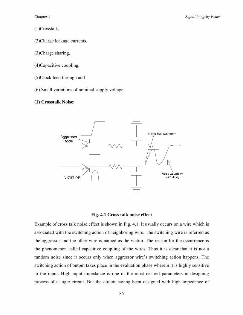
Chapter 4 Signal integrity issues
85
(1)Crosstalk,
(2)Charge leakage currents,
(3)Charge sharing,
(4)Capacitive coupling,
(5)Clock feed through and
(6) Small variations of nominal supply voltage.
(1) Crosstalk Noise:
Fig. 4.1 Cross talk noise effect
Example of cross talk noise effect is shown in Fig. 4.1. It usually occurs on a wire which is
associated with the switching action of neighboring wire. The switching wire is referred as
the aggressor and the other wire is named as the victim. The reason for the occurrence is
the phenomenon called capacitive coupling of the wires. Thus it is clear that it is not a
random noise since it occurs only when aggressor wire’s switching action happens. The
switching action of output takes place in the evaluation phase wherein it is highly sensitive
to the input. High input impedance is one of the most desired parameters in designing
process of a logic circuit. But the circuit having been designed with high impedance of
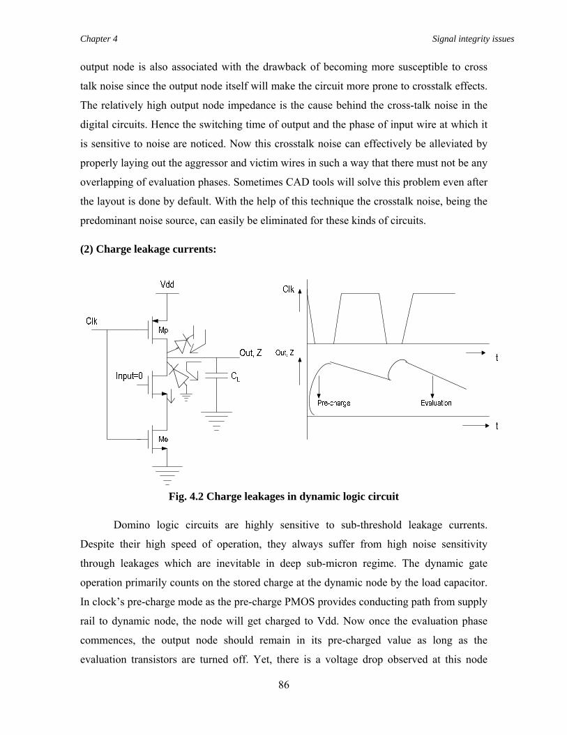
Chapter 4 Signal integrity issues
86
output node is also associated with the drawback of becoming more susceptible to cross
talk noise since the output node itself will make the circuit more prone to crosstalk effects.
The relatively high output node impedance is the cause behind the cross-talk noise in the
digital circuits. Hence the switching time of output and the phase of input wire at which it
is sensitive to noise are noticed. Now this crosstalk noise can effectively be alleviated by
properly laying out the aggressor and victim wires in such a way that there must not be any
overlapping of evaluation phases. Sometimes CAD tools will solve this problem even after
the layout is done by default. With the help of this technique the crosstalk noise, being the
predominant noise source, can easily be eliminated for these kinds of circuits.
(2) Charge leakage currents:
Fig. 4.2 Charge leakages in dynamic logic circuit
Domino logic circuits are highly sensitive to sub-threshold leakage currents.
Despite their high speed of operation, they always suffer from high noise sensitivity
through leakages which are inevitable in deep sub-micron regime. The dynamic gate
operation primarily counts on the stored charge at the dynamic node by the load capacitor.
In clock’s pre-charge mode as the pre-charge PMOS provides conducting path from supply
rail to dynamic node, the node will get charged to Vdd. Now once the evaluation phase
commences, the output node should remain in its pre-charged value as long as the
evaluation transistors are turned off. Yet, there is a voltage drop observed at this node
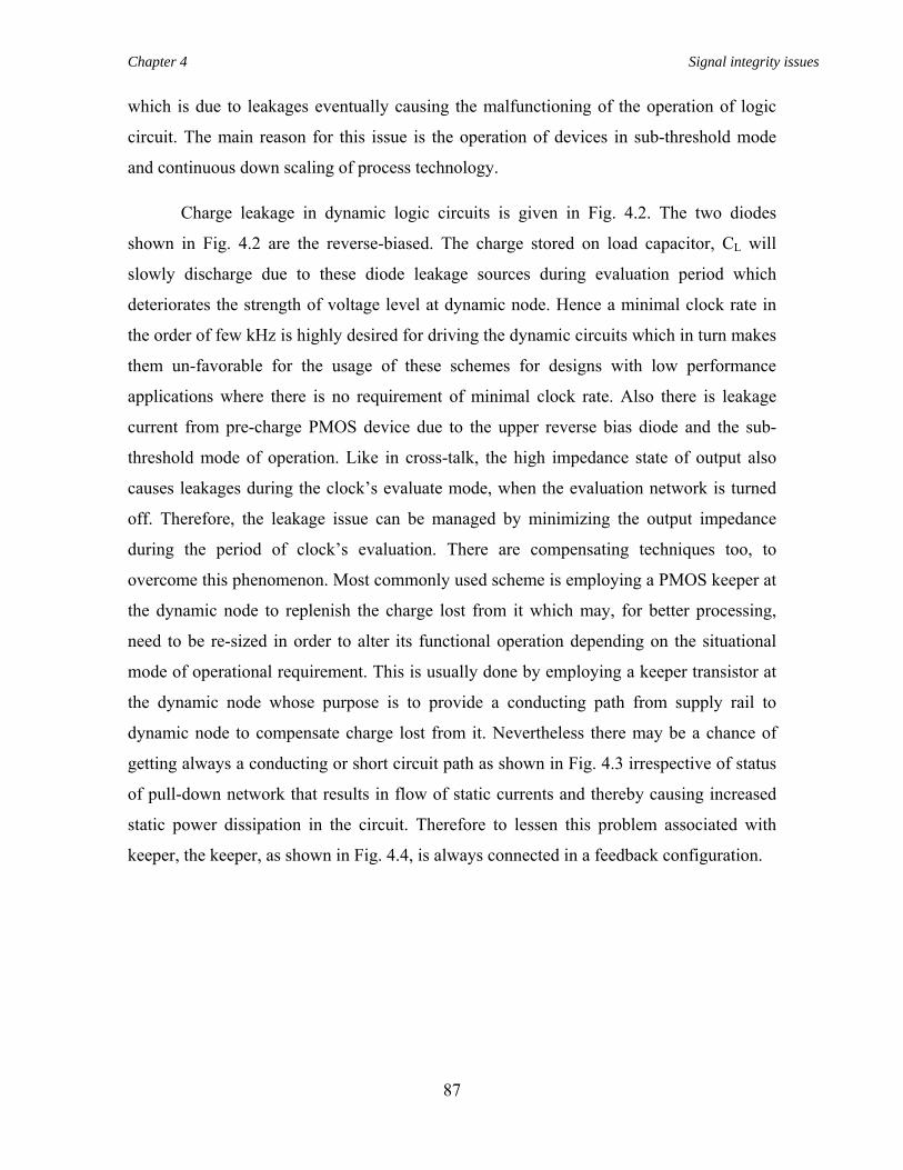
Chapter 4 Signal integrity issues
87
which is due to leakages eventually causing the malfunctioning of the operation of logic
circuit. The main reason for this issue is the operation of devices in sub-threshold mode
and continuous down scaling of process technology.
Charge leakage in dynamic logic circuits is given in Fig. 4.2. The two diodes
shown in Fig. 4.2 are the reverse-biased. The charge stored on load capacitor, CL will
slowly discharge due to these diode leakage sources during evaluation period which
deteriorates the strength of voltage level at dynamic node. Hence a minimal clock rate in
the order of few kHz is highly desired for driving the dynamic circuits which in turn makes
them un-favorable for the usage of these schemes for designs with low performance
applications where there is no requirement of minimal clock rate. Also there is leakage
current from pre-charge PMOS device due to the upper reverse bias diode and the sub-
threshold mode of operation. Like in cross-talk, the high impedance state of output also
causes leakages during the clock’s evaluate mode, when the evaluation network is turned
off. Therefore, the leakage issue can be managed by minimizing the output impedance
during the period of clock’s evaluation. There are compensating techniques too, to
overcome this phenomenon. Most commonly used scheme is employing a PMOS keeper at
the dynamic node to replenish the charge lost from it which may, for better processing,
need to be re-sized in order to alter its functional operation depending on the situational
mode of operational requirement. This is usually done by employing a keeper transistor at
the dynamic node whose purpose is to provide a conducting path from supply rail to
dynamic node to compensate charge lost from it. Nevertheless there may be a chance of
getting always a conducting or short circuit path as shown in Fig. 4.3 irrespective of status
of pull-down network that results in flow of static currents and thereby causing increased
static power dissipation in the circuit. Therefore to lessen this problem associated with
keeper, the keeper, as shown in Fig. 4.4, is always connected in a feedback configuration.
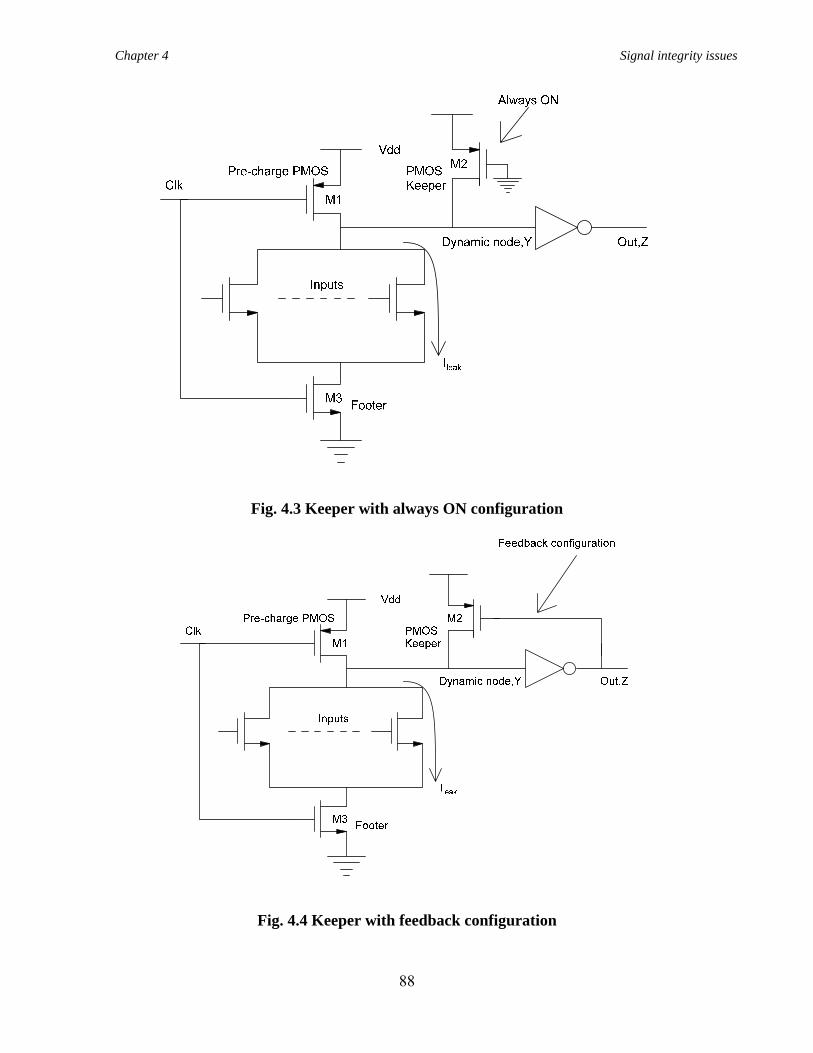
Chapter 4 Signal integrity issues
88
Fig. 4.3 Keeper with always ON configuration
Fig. 4.4 Keeper with feedback configuration
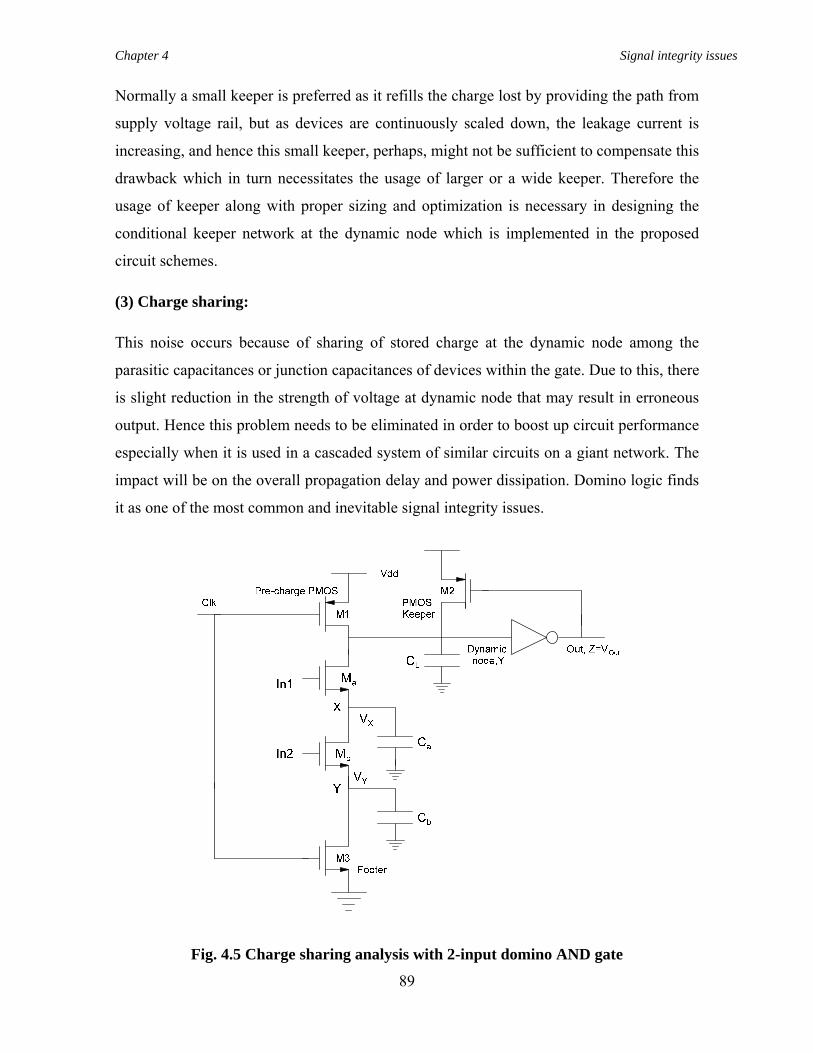
Chapter 4 Signal integrity issues
89
Normally a small keeper is preferred as it refills the charge lost by providing the path from
supply voltage rail, but as devices are continuously scaled down, the leakage current is
increasing, and hence this small keeper, perhaps, might not be sufficient to compensate this
drawback which in turn necessitates the usage of larger or a wide keeper. Therefore the
usage of keeper along with proper sizing and optimization is necessary in designing the
conditional keeper network at the dynamic node which is implemented in the proposed
circuit schemes.
(3) Charge sharing:
This noise occurs because of sharing of stored charge at the dynamic node among the
parasitic capacitances or junction capacitances of devices within the gate. Due to this, there
is slight reduction in the strength of voltage at dynamic node that may result in erroneous
output. Hence this problem needs to be eliminated in order to boost up circuit performance
especially when it is used in a cascaded system of similar circuits on a giant network. The
impact will be on the overall propagation delay and power dissipation. Domino logic finds
it as one of the most common and inevitable signal integrity issues.
Fig. 4.5 Charge sharing analysis with 2-input domino AND gate
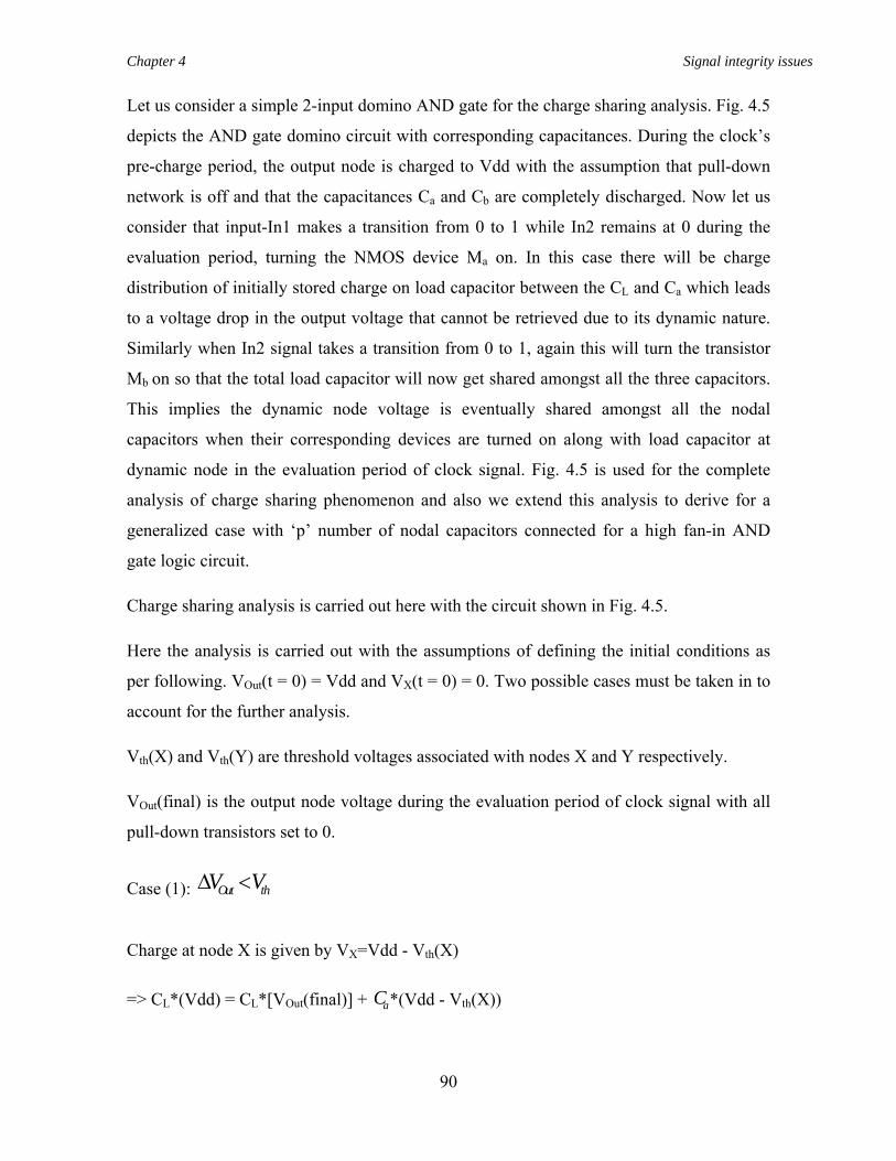
Chapter 4 Signal integrity issues
90
Let us consider a simple 2-input domino AND gate for the charge sharing analysis. Fig. 4.5
depicts the AND gate domino circuit with corresponding capacitances. During the clock’s
pre-charge period, the output node is charged to Vdd with the assumption that pull-down
network is off and that the capacitances Ca and Cb are completely discharged. Now let us
consider that input-In1 makes a transition from 0 to 1 while In2 remains at 0 during the
evaluation period, turning the NMOS device Ma on. In this case there will be charge
distribution of initially stored charge on load capacitor between the CL and Ca which leads
to a voltage drop in the output voltage that cannot be retrieved due to its dynamic nature.
Similarly when In2 signal takes a transition from 0 to 1, again this will turn the transistor
Mb on so that the total load capacitor will now get shared amongst all the three capacitors.
This implies the dynamic node voltage is eventually shared amongst all the nodal
capacitors when their corresponding devices are turned on along with load capacitor at
dynamic node in the evaluation period of clock signal. Fig. 4.5 is used for the complete
analysis of charge sharing phenomenon and also we extend this analysis to derive for a
generalized case with ‘p’ number of nodal capacitors connected for a high fan-in AND
gate logic circuit.
Charge sharing analysis is carried out here with the circuit shown in Fig. 4.5.
Here the analysis is carried out with the assumptions of defining the initial conditions as
per following. VOut(t = 0) = Vdd and VX(t = 0) = 0. Two possible cases must be taken in to
account for the further analysis.
Vth(X) and Vth(Y) are threshold voltages associated with nodes X and Y respectively.
VOut(final) is the output node voltage during the evaluation period of clock signal with all
pull-down transistors set to 0.
Case (1): Out thV VΔ <
Charge at node X is given by VX=Vdd - Vth(X)
=> CL*(Vdd) = CL*[VOut(final)] + aC *(Vdd - Vth(X))
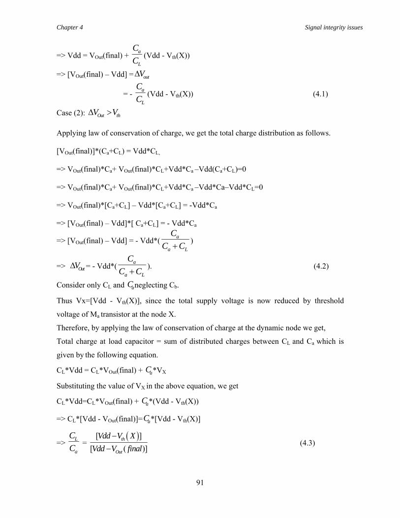
Chapter 4 Signal integrity issues
91
=> Vdd = VOut(final) + a
L
CC (Vdd - Vth(X))
=> [VOut(final) – Vdd] = outVΔ
= - a
L
CC (Vdd - Vth(X)) (4.1)
Case (2): Out thV VΔ > Applying law of conservation of charge, we get the total charge distribution as follows. [VOut(final)]*(Ca+CL) = Vdd*CL, => VOut(final)*Ca+ VOut(final)*CL+Vdd*Ca –Vdd(Ca+CL)=0 => VOut(final)*Ca+ VOut(final)*CL+Vdd*Ca –Vdd*Ca–Vdd*CL=0 => VOut(final)*[Ca+CL] – Vdd*[Ca+CL] = -Vdd*Ca => [VOut(final) – Vdd]*[ Ca+CL] = - Vdd*Ca
=> [VOut(final) – Vdd] = - Vdd*( a
a L
CC C+ )
=> OutVΔ = - Vdd*( a
a L
CC C+ ). (4.2)
Consider only CL and aC neglecting Cb.
Thus Vx=[Vdd - Vth(X)], since the total supply voltage is now reduced by threshold
voltage of Ma transistor at the node X.
Therefore, by applying the law of conservation of charge at the dynamic node we get,
Total charge at load capacitor = sum of distributed charges between CL and Ca which is
given by the following equation.
CL*Vdd = CL*VOut(final) + aC *VX
Substituting the value of VX in the above equation, we get
CL*Vdd=CL*VOut(final) + aC *(Vdd - Vth(X))
=> CL*[Vdd - VOut(final)]= aC *[Vdd - Vth(X)]
=> L
a
CC =
( )[ ][ ( )]
th
Out
Vdd XVdd V fin
Val
−−
(4.3)
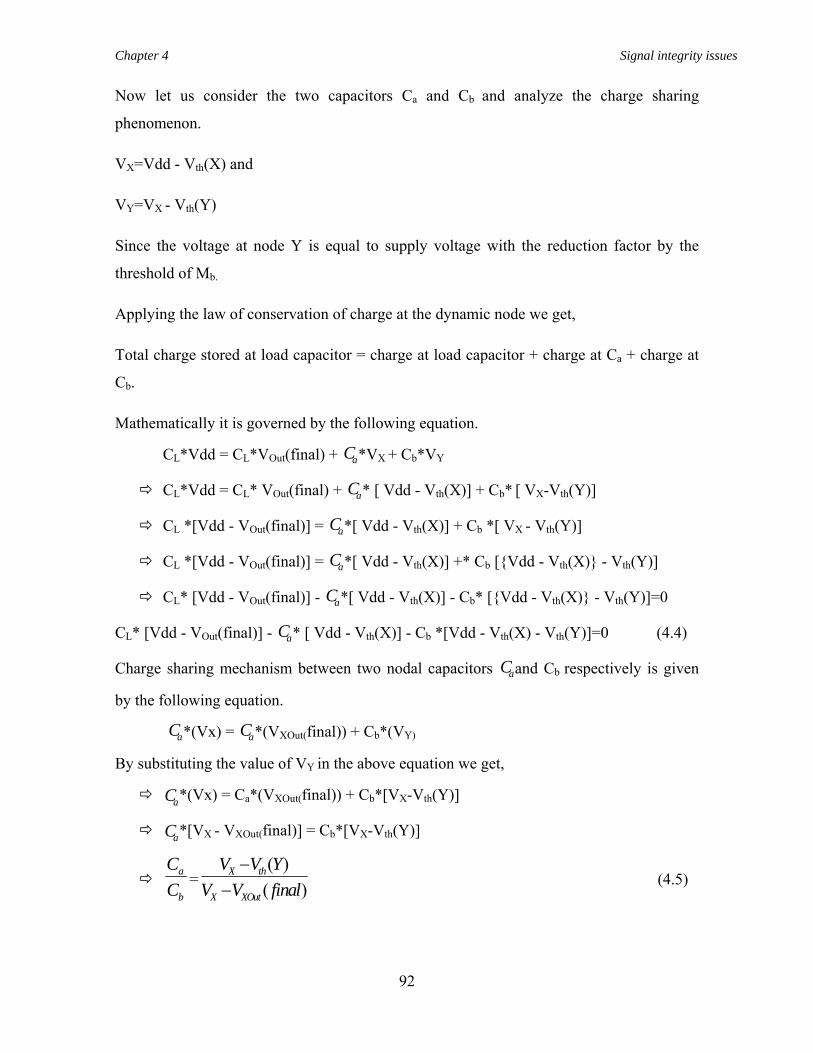
Chapter 4 Signal integrity issues
92
Now let us consider the two capacitors Ca and Cb and analyze the charge sharing
phenomenon.
VX=Vdd - Vth(X) and
VY=VX - Vth(Y)
Since the voltage at node Y is equal to supply voltage with the reduction factor by the
threshold of Mb.
Applying the law of conservation of charge at the dynamic node we get,
Total charge stored at load capacitor = charge at load capacitor + charge at Ca + charge at
Cb.
Mathematically it is governed by the following equation.
CL*Vdd = CL*VOut(final) + aC *VX + Cb*VY
CL*Vdd = CL* VOut(final) + aC * [ Vdd - Vth(X)] + Cb* [ VX-Vth(Y)]
CL *[Vdd - VOut(final)] = aC *[ Vdd - Vth(X)] + Cb *[ VX - Vth(Y)]
CL *[Vdd - VOut(final)] = aC *[ Vdd - Vth(X)] +* Cb [{Vdd - Vth(X)} - Vth(Y)]
CL* [Vdd - VOut(final)] - aC *[ Vdd - Vth(X)] - Cb* [{Vdd - Vth(X)} - Vth(Y)]=0
CL* [Vdd - VOut(final)] - aC * [ Vdd - Vth(X)] - Cb *[Vdd - Vth(X) - Vth(Y)]=0 (4.4)
Charge sharing mechanism between two nodal capacitors aC and Cb respectively is given
by the following equation.
aC *(Vx) = aC *(VXOut(final)) + Cb*(VY)
By substituting the value of VY in the above equation we get,
aC *(Vx) = Ca*(VXOut(final)) + Cb*[VX-Vth(Y)]
aC *[VX - VXOut(final)] = Cb*[VX-Vth(Y)]
a
b
CC =
( )( )
X th
X XOut
V V YV V final
−−
(4.5)
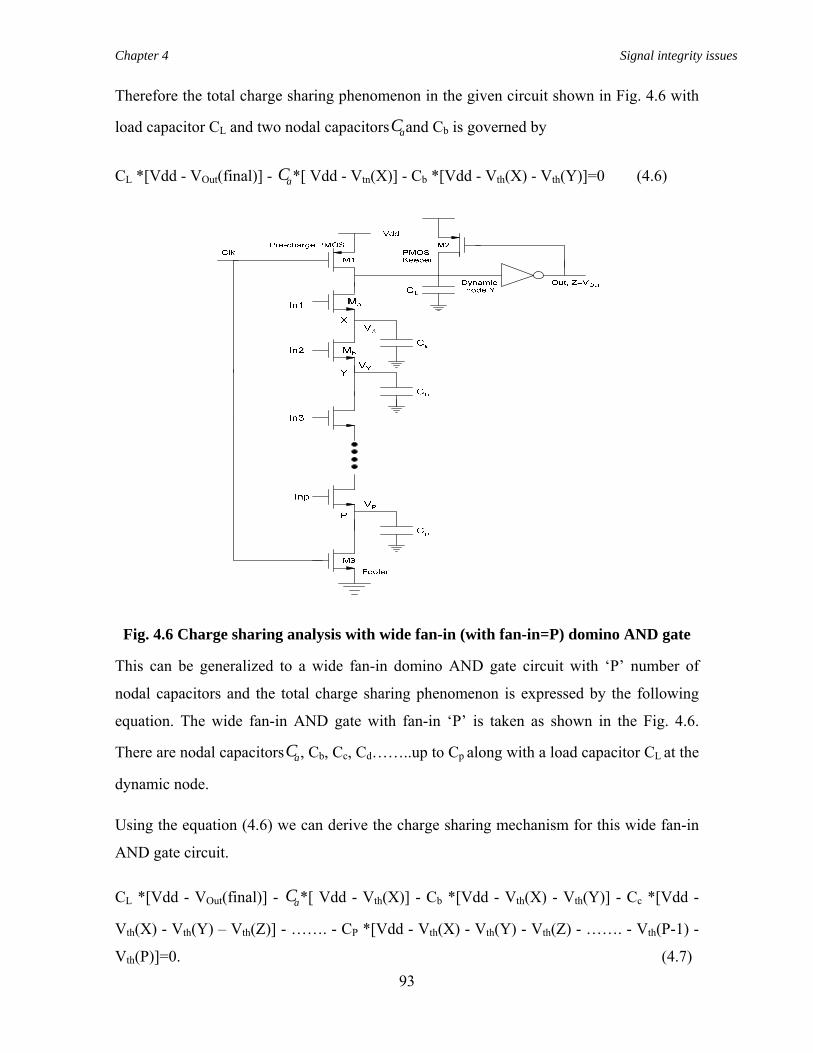
Chapter 4 Signal integrity issues
93
Therefore the total charge sharing phenomenon in the given circuit shown in Fig. 4.6 with
load capacitor CL and two nodal capacitors aC and Cb is governed by
CL *[Vdd - VOut(final)] - aC *[ Vdd - Vtn(X)] - Cb *[Vdd - Vth(X) - Vth(Y)]=0 (4.6)
Fig. 4.6 Charge sharing analysis with wide fan-in (with fan-in=P) domino AND gate
This can be generalized to a wide fan-in domino AND gate circuit with ‘P’ number of
nodal capacitors and the total charge sharing phenomenon is expressed by the following
equation. The wide fan-in AND gate with fan-in ‘P’ is taken as shown in the Fig. 4.6.
There are nodal capacitors aC , Cb, Cc, Cd……..up to Cp along with a load capacitor CL at the
dynamic node.
Using the equation (4.6) we can derive the charge sharing mechanism for this wide fan-in
AND gate circuit.
CL *[Vdd - VOut(final)] - aC *[ Vdd - Vth(X)] - Cb *[Vdd - Vth(X) - Vth(Y)] - Cc *[Vdd -
Vth(X) - Vth(Y) – Vth(Z)] - ……. - CP *[Vdd - Vth(X) - Vth(Y) - Vth(Z) - ……. - Vth(P-1) -
Vth(P)]=0. (4.7)
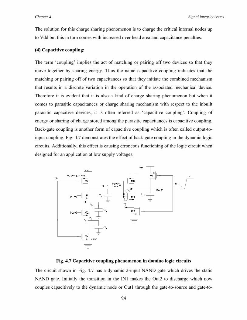
Chapter 4 Signal integrity issues
94
The solution for this charge sharing phenomenon is to charge the critical internal nodes up
to Vdd but this in turn comes with increased over head area and capacitance penalties.
(4) Capacitive coupling:
The term ‘coupling’ implies the act of matching or pairing off two devices so that they
move together by sharing energy. Thus the name capacitive coupling indicates that the
matching or pairing off of two capacitances so that they initiate the combined mechanism
that results in a discrete variation in the operation of the associated mechanical device.
Therefore it is evident that it is also a kind of charge sharing phenomenon but when it
comes to parasitic capacitances or charge sharing mechanism with respect to the inbuilt
parasitic capacitive devices, it is often referred as ‘capacitive coupling’. Coupling of
energy or sharing of charge stored among the parasitic capacitances is capacitive coupling.
Back-gate coupling is another form of capacitive coupling which is often called output-to-
input coupling. Fig. 4.7 demonstrates the effect of back-gate coupling in the dynamic logic
circuits. Additionally, this effect is causing erroneous functioning of the logic circuit when
designed for an application at low supply voltages.
Fig. 4.7 Capacitive coupling phenomenon in domino logic circuits
The circuit shown in Fig. 4.7 has a dynamic 2-input NAND gate which drives the static
NAND gate. Initially the transition in the IN1 makes the Out2 to discharge which now
couples capacitively to the dynamic node or Out1 through the gate-to-source and gate-to-
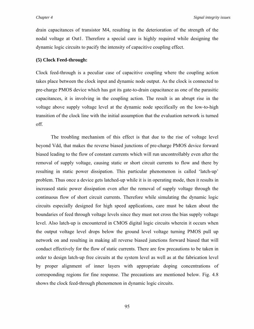
Chapter 4 Signal integrity issues
95
drain capacitances of transistor M4, resulting in the deterioration of the strength of the
nodal voltage at Out1. Therefore a special care is highly required while designing the
dynamic logic circuits to pacify the intensity of capacitive coupling effect.
(5) Clock Feed-through:
Clock feed-through is a peculiar case of capacitive coupling where the coupling action
takes place between the clock input and dynamic node output. As the clock is connected to
pre-charge PMOS device which has got its gate-to-drain capacitance as one of the parasitic
capacitances, it is involving in the coupling action. The result is an abrupt rise in the
voltage above supply voltage level at the dynamic node specifically on the low-to-high
transition of the clock line with the initial assumption that the evaluation network is turned
off.
The troubling mechanism of this effect is that due to the rise of voltage level
beyond Vdd, that makes the reverse biased junctions of pre-charge PMOS device forward
biased leading to the flow of constant currents which will run uncontrollably even after the
removal of supply voltage, causing static or short circuit currents to flow and there by
resulting in static power dissipation. This particular phenomenon is called ‘latch-up’
problem. Thus once a device gets latched-up while it is in operating mode, then it results in
increased static power dissipation even after the removal of supply voltage through the
continuous flow of short circuit currents. Therefore while simulating the dynamic logic
circuits especially designed for high speed applications, care must be taken about the
boundaries of feed through voltage levels since they must not cross the bias supply voltage
level. Also latch-up is encountered in CMOS digital logic circuits wherein it occurs when
the output voltage level drops below the ground level voltage turning PMOS pull up
network on and resulting in making all reverse biased junctions forward biased that will
conduct effectively for the flow of static currents. There are few precautions to be taken in
order to design latch-up free circuits at the system level as well as at the fabrication level
by proper alignment of inner layers with appropriate doping concentrations of
corresponding regions for fine response. The precautions are mentioned below. Fig. 4.8
shows the clock feed-through phenomenon in dynamic logic circuits.

Chapter 4 Signal integrity issues
96
Fig. 4.8 Clock feed-through phenomenon dynamic logic circuits
Precautions:
1. Always make sure that the power supply rails must be off before plugging a board.
2. Usage of ESD (Electro Static Discharge) protection layers on all electronic
appliances carefully to protect the designs from electrostatic currents which can
trigger latch-up associated with input-output pads.
3. Designs must not get exposed to radiations including X-rays, cosmic rays which
can produce electron-hole pairs as they hit the design chip through penetration
since these carriers in turn generate substrate or well currents.
4. Abrupt occurrence of transients on the supply or ground rail which may likely to
happen if more numbers of transistors are switching simultaneously, can trigger the
latch-up phenomenon in the designed circuit.
(6)Small variations from supply voltage:
This is associated with latch-up mechanism. Owing to the glitches in the circuit, there
might be minute variations occurring in the nominal supply voltages which may sometimes
cause severe iterative issues like latch-up problems that will repeatedly run for long time
uncontrollably causing leakages and static currents to flow inside the device and there by
resulting in static power dissipation. This may be due to the mismatching in the alignment
of physical layers of devices while processing the lithography, etching and other
fabrication steps involved. Therefore, proper care must be taken in order to avoid such
Chapter 4 Signal integrity issues
97
iterative cyclic problems in the circuits, while processing the device and arranging the
inner layers through several physical fabrication steps. The amplitude of glitches will also
show its considerable impact on the operation of the circuit that runs especially with low
bias voltage. Also the voltage fluctuation at the ground level results in supply voltage
variations in few cases. Hence the variations from supply voltages must be eliminated to
get an error-free mechanism of the designed logic circuits.
4.3 Related work on lector power reduction technique
In static CMOS circuit designs, scaling is meant for reducing threshold voltage, device
dimensions (typically channel length), bias voltage and increasing speed of operation. Due
to down scaling of process technology the channel length is getting shortened which results
in speeding up the operation. Besides this, there is rapid increment in the flow of inevitable
sub-threshold leakage currents in the sub-threshold region in deep-sub-micron. Thus the
continuous reduction of the threshold voltage causes significant increment in sub-threshold
leakage current which results in static or leakage power dissipation. In this chapter,
existing scheme known as “leakage control transistor (domino lector or domino LCT)” is
described to minimize the leakages without affecting dynamic power consumption [60].
This lector scheme introduces two transistors called leakage control transistors of one
PMOS and one NMOS each within the implementation of this technique to cut-down the
leakage current through the operation of triggering each gate terminal of leakage control
device by source terminal of other device.
This peculiar arrangement keeps one of the LCTs in cut-off region for any
combination of inputs which increases the effective equivalent resistance of the conducting
path from Vdd rail to ground rail, causing significant reduction in sub-threshold leakage
currents. Before adding these LCTs to control leakage currents in the circuit, initially the
gate-level net list of the circuit must be converted to a static CMOS implementation. The
efficient functioning in both switching and non-switching modes of the circuit is the merit
feature of lector technique which results in mitigating the leakages efficiently when
compared to other schemes. Added to this, the proposed domino lector technique
overcomes the limitations by other benchmark methods for the reduction of leakage.
Copious schemes for reduction of leakage power have been presented in the literature. The
Chapter 4 Signal integrity issues
98
proposal in [67] demonstrates to make use of the dependent relation of the sub-threshold
leakage current on the gate inputs. By adding an extra control network, the leakages can be
controlled when it is in idle state and brought to its original operating state when activated
again. This implies that there must be a sense of history to store the original data as the
circuit is activated again from idle state which needs to include memory storage elements
like latches or flip-flops and thereby increasing the overhead area of the circuit [8]. Power
gating and clock gating are the other system level schemes used in some designs to reduce
the power by turning off the supply voltage to unusable logic blocks where they make use
of sleep transistors either NMOS or PMOS in the path from supply rail to ground rail.
When the circuit is in active mode then sleep transistor will be turned on by a sleep signal
while in other case, circuit’s idle state, sleep transistor will be turned off and thereby
creating virtual rails of power supply and ground nodes. Therefore, when the circuit is in
active mode, the switching speed gets affected. Thus, the idle regions need to be identified
along with the generation of sleep signals that trigger the sleep devices. This could be
achieved by adding an extra hardware circuit which in turn consumes much power.
MTCMOS (Multiple threshold voltage CMOS) scheme is other leakage reduction
technique presented in [11, 12]. These devices are working at lower threshold voltages and
footer transistor higher threshold NMOS transistor. The gating transistor operates as sleep
transistor. Noise margins are reduced due to reverse conduction path [4]. Also, the
drawback is that degradation in the performance due to series connected high threshold
transistors in the switching paths. Modified version of MTCMOS technique is dual
threshold technique that consists of transistors with two different threshold voltages.
Critical path is evaluated by lower threshold transistors. Higher threshold voltage
transistors are employed for gates which are connected in non-critical path [4, 13, 14]. The
similarity between MTCMOS and Dual threshold voltage technique is that both require an
additional mask for fabricating these devices on wafers according to their threshold
voltages which makes it complex. Clock gating and power gating techniques for lowering
power dissipation are most appropriate and compatible for system level design but not for
circuit level. Another limitation is slow-latency as some time is required for returning to
normal condition for the sub-circuit because when the activation is done, immediately they
are not turned on.
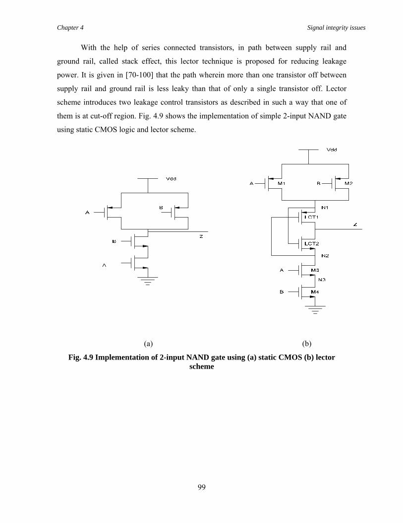
Chapter 4 Signal integrity issues
99
With the help of series connected transistors, in path between supply rail and
ground rail, called stack effect, this lector technique is proposed for reducing leakage
power. It is given in [70-100] that the path wherein more than one transistor off between
supply rail and ground rail is less leaky than that of only a single transistor off. Lector
scheme introduces two leakage control transistors as described in such a way that one of
them is at cut-off region. Fig. 4.9 shows the implementation of simple 2-input NAND gate
using static CMOS logic and lector scheme.
(a) (b)
Fig. 4.9 Implementation of 2-input NAND gate using (a) static CMOS (b) lector scheme
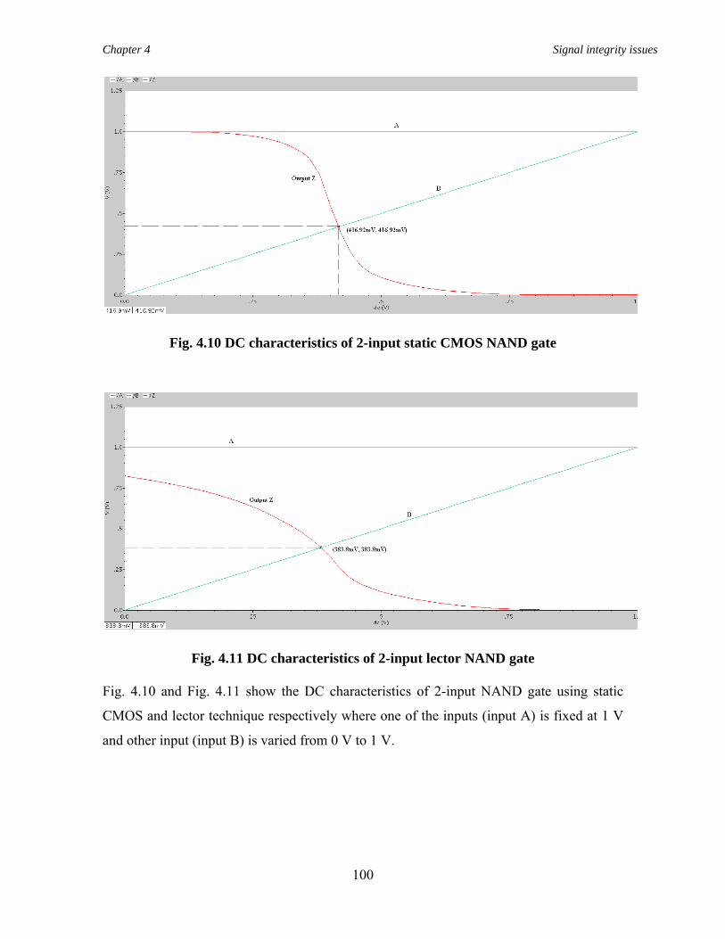
Chapter 4 Signal integrity issues
100
Fig. 4.10 DC characteristics of 2-input static CMOS NAND gate
Fig. 4.11 DC characteristics of 2-input lector NAND gate
Fig. 4.10 and Fig. 4.11 show the DC characteristics of 2-input NAND gate using static
CMOS and lector technique respectively where one of the inputs (input A) is fixed at 1 V
and other input (input B) is varied from 0 V to 1 V.
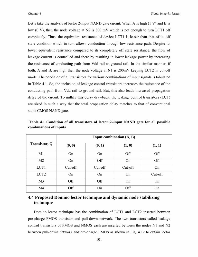
Chapter 4 Signal integrity issues
101
Let’s take the analysis of lector 2-input NAND gate circuit. When A is high (1 V) and B is
low (0 V), then the node voltage at N2 is 800 mV which is not enough to turn LCT1 off
completely. Thus, the equivalent resistance of device LCT1 is lesser than that of its off
state condition which in turn allows conduction through low resistance path. Despite its
lower equivalent resistance compared to its completely off state resistance, the flow of
leakage current is controlled and there by resulting in lower leakage power by increasing
the resistance of conducting path from Vdd rail to ground rail. In the similar manner, if
both, A and B, are high then the node voltage at N1 is 200mV keeping LCT2 in cut-off
mode. The condition of all transistors for various combinations of input signals is tabulated
in Table 4.1. So, the inclusion of leakage control transistors increases the resistance of the
conducting path from Vdd rail to ground rail. But, this also leads increased propagation
delay of the circuit. To nullify this delay drawback, the leakage control transistors (LCT)
are sized in such a way that the total propagation delay matches to that of conventional
static CMOS NAND gate.
Table 4.1 Condition of all transistors of lector 2–input NAND gate for all possible combinations of inputs
Transistor, Q
Input combination (A, B)
(0, 0) (0, 1) (1, 0) (1, 1)
M1 On On Off Off
M2 On Off On Off
LCT1 Cut-off Cut-off Cut-off On
LCT2 On On On Cut-off
M3 Off Off On On
M4 Off On Off On
4.4 Proposed Domino lector technique and dynamic node stabilizing technique
Domino lector technique has the combination of LCT1 and LCT2 inserted between
pre-charge PMOS transistor and pull-down network. The two transistors called leakage
control transistors of PMOS and NMOS each are inserted between the nodes N1 and N2
between pull-down network and pre-charge PMOS as shown in Fig. 4.12 to obtain lector
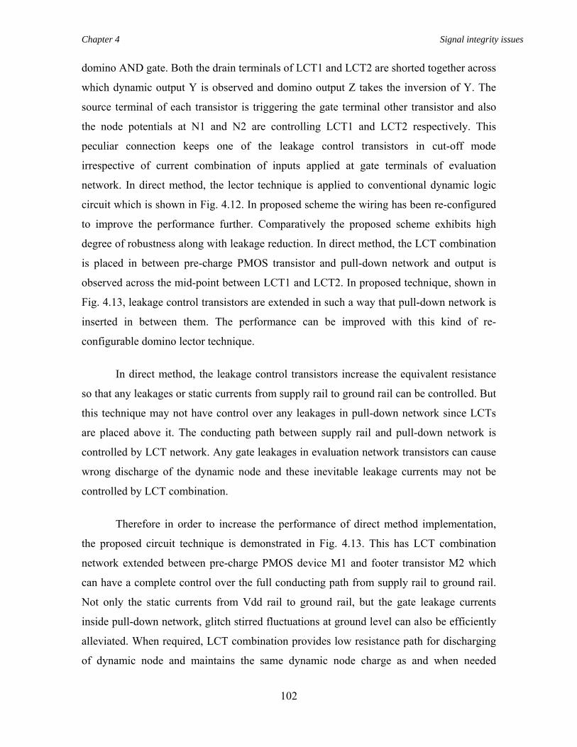
Chapter 4 Signal integrity issues
102
domino AND gate. Both the drain terminals of LCT1 and LCT2 are shorted together across
which dynamic output Y is observed and domino output Z takes the inversion of Y. The
source terminal of each transistor is triggering the gate terminal other transistor and also
the node potentials at N1 and N2 are controlling LCT1 and LCT2 respectively. This
peculiar connection keeps one of the leakage control transistors in cut-off mode
irrespective of current combination of inputs applied at gate terminals of evaluation
network. In direct method, the lector technique is applied to conventional dynamic logic
circuit which is shown in Fig. 4.12. In proposed scheme the wiring has been re-configured
to improve the performance further. Comparatively the proposed scheme exhibits high
degree of robustness along with leakage reduction. In direct method, the LCT combination
is placed in between pre-charge PMOS transistor and pull-down network and output is
observed across the mid-point between LCT1 and LCT2. In proposed technique, shown in
Fig. 4.13, leakage control transistors are extended in such a way that pull-down network is
inserted in between them. The performance can be improved with this kind of re-
configurable domino lector technique.
In direct method, the leakage control transistors increase the equivalent resistance
so that any leakages or static currents from supply rail to ground rail can be controlled. But
this technique may not have control over any leakages in pull-down network since LCTs
are placed above it. The conducting path between supply rail and pull-down network is
controlled by LCT network. Any gate leakages in evaluation network transistors can cause
wrong discharge of the dynamic node and these inevitable leakage currents may not be
controlled by LCT combination.
Therefore in order to increase the performance of direct method implementation,
the proposed circuit technique is demonstrated in Fig. 4.13. This has LCT combination
network extended between pre-charge PMOS device M1 and footer transistor M2 which
can have a complete control over the full conducting path from supply rail to ground rail.
Not only the static currents from Vdd rail to ground rail, but the gate leakage currents
inside pull-down network, glitch stirred fluctuations at ground level can also be efficiently
alleviated. When required, LCT combination provides low resistance path for discharging
of dynamic node and maintains the same dynamic node charge as and when needed
Chapter 4 Signal integrity issues
103
depending upon the current combination of the inputs to the pull-down network transistors.
Apart from LCT network, clock is also acting as driving element. The drain potential of
footer transistor M2 is triggering the LCT1 and the drain potential of pre-charge PMOS
device M1 is controlling LCT2.
Fig. 4.12 Direct method of implementing lector domino logic circuit
Fig. 4.13 shows the implementation of proposed lector domino circuit technique and Fig.
4.14 represents the simulation result of proposed lector 2-input domino OR gate logic
circuit. Potentials at nodes N1, N2 and the corresponding change in the voltage levels
along with pre-charge and evaluation phases of clock signal can be observed from the
simulation graph. Output-Z is following logic OR gate operation of two applied gate inputs
of pull-down network. Transistors M1 and M2 are driven by clock signal and LCT1 and
LCT2 are triggered by nodal potentials at N1 and N2 respectively.
In pre-charge phase, M1 is turned on and M2 is turned off. Node N1 is at Vdd which is
sufficient to turn LCT2 on and node N2 is at 127.7mV which is enough to turn LCT1 on.
Therefore there exists a conducting path from supply rail to dynamic node Y that charges
node Y to Vdd. Since LCT2 is on and footer M2 is off, there is no discharging path during
pre-charge phase irrespective of status of current combination of inputs to pull-down
network. LCT1 and LCT2 are controlling the path between nodes N1 and N2 so that any
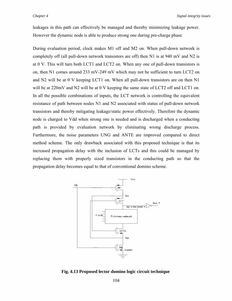
Chapter 4 Signal integrity issues
104
leakages in this path can effectively be managed and thereby minimizing leakage power.
However the dynamic node is able to produce strong one during pre-charge phase.
During evaluation period, clock makes M1 off and M2 on. When pull-down network is
completely off (all pull-down network transistors are off) then N1 is at 940 mV and N2 is
at 0 V. This will turn both LCT1 and LCT2 on. When any one of pull-down transistors is
on, then N1 comes around 233 mV-249 mV which may not be sufficient to turn LCT2 on
and N2 will be at 0 V keeping LCT1 on. When all pull-down transistors are on then N1
will be at 220mV and N2 will be at 0 V keeping the same state of LCT2 off and LCT1 on.
In all the possible combinations of inputs, the LCT network is controlling the equivalent
resistance of path between nodes N1 and N2 associated with status of pull-down network
transistors and thereby mitigating leakage/static power effectively. Therefore the dynamic
node is charged to Vdd when strong one is needed and is discharged when a conducting
path is provided by evaluation network by eliminating wrong discharge process.
Furthermore, the noise parameters UNG and ANTE are improved compared to direct
method scheme. The only drawback associated with this proposed technique is that its
increased propagation delay with the inclusion of LCTs and this could be managed by
replacing them with properly sized transistors in the conducting path so that the
propagation delay becomes equal to that of conventional domino scheme.
Fig. 4.13 Proposed lector domino logic circuit technique
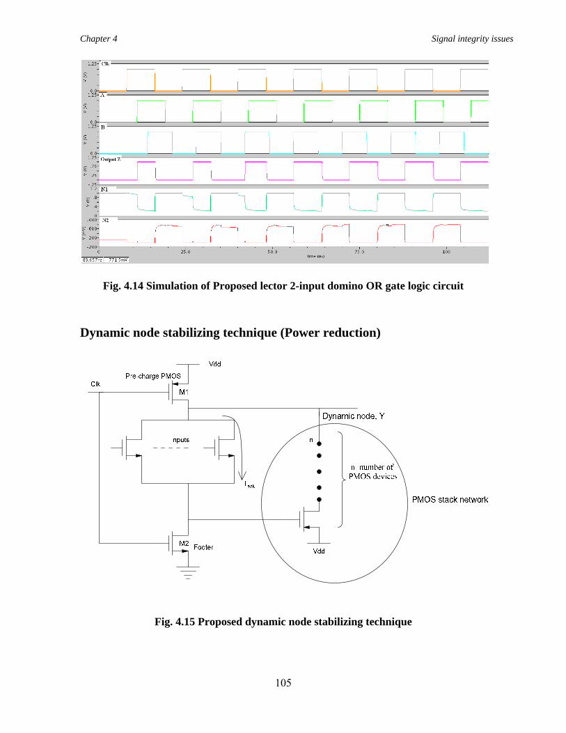
Chapter 4 Signal integrity issues
105
Fig. 4.14 Simulation of Proposed lector 2-input domino OR gate logic circuit
Dynamic node stabilizing technique (Power reduction)
Fig. 4.15 Proposed dynamic node stabilizing technique
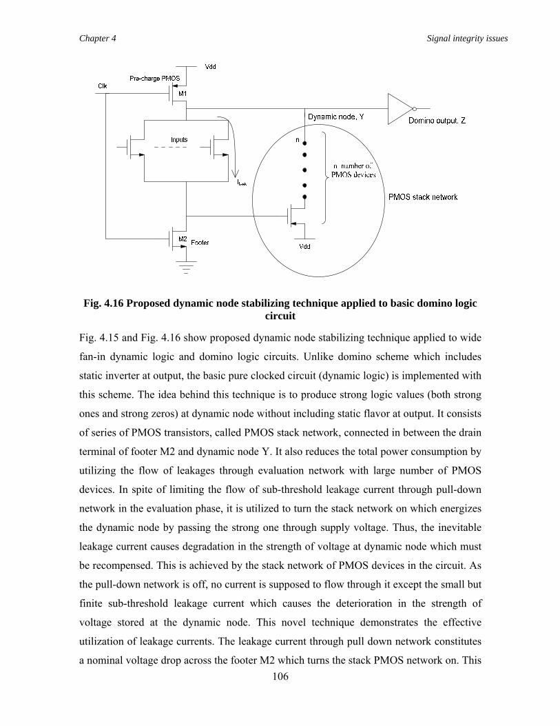
Chapter 4 Signal integrity issues
106
Fig. 4.16 Proposed dynamic node stabilizing technique applied to basic domino logic circuit
Fig. 4.15 and Fig. 4.16 show proposed dynamic node stabilizing technique applied to wide
fan-in dynamic logic and domino logic circuits. Unlike domino scheme which includes
static inverter at output, the basic pure clocked circuit (dynamic logic) is implemented with
this scheme. The idea behind this technique is to produce strong logic values (both strong
ones and strong zeros) at dynamic node without including static flavor at output. It consists
of series of PMOS transistors, called PMOS stack network, connected in between the drain
terminal of footer M2 and dynamic node Y. It also reduces the total power consumption by
utilizing the flow of leakages through evaluation network with large number of PMOS
devices. In spite of limiting the flow of sub-threshold leakage current through pull-down
network in the evaluation phase, it is utilized to turn the stack network on which energizes
the dynamic node by passing the strong one through supply voltage. Thus, the inevitable
leakage current causes degradation in the strength of voltage at dynamic node which must
be recompensed. This is achieved by the stack network of PMOS devices in the circuit. As
the pull-down network is off, no current is supposed to flow through it except the small but
finite sub-threshold leakage current which causes the deterioration in the strength of
voltage stored at the dynamic node. This novel technique demonstrates the effective
utilization of leakage currents. The leakage current through pull down network constitutes
a nominal voltage drop across the footer M2 which turns the stack PMOS network on. This
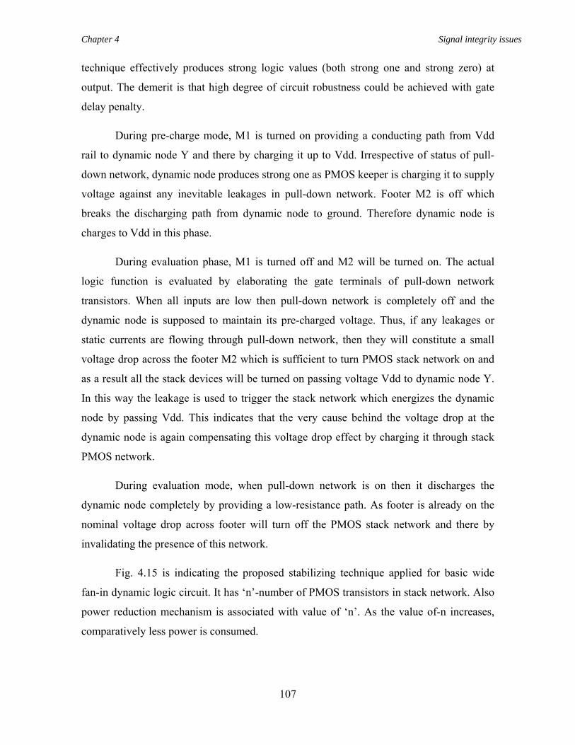
Chapter 4 Signal integrity issues
107
technique effectively produces strong logic values (both strong one and strong zero) at
output. The demerit is that high degree of circuit robustness could be achieved with gate
delay penalty.
During pre-charge mode, M1 is turned on providing a conducting path from Vdd
rail to dynamic node Y and there by charging it up to Vdd. Irrespective of status of pull-
down network, dynamic node produces strong one as PMOS keeper is charging it to supply
voltage against any inevitable leakages in pull-down network. Footer M2 is off which
breaks the discharging path from dynamic node to ground. Therefore dynamic node is
charges to Vdd in this phase.
During evaluation phase, M1 is turned off and M2 will be turned on. The actual
logic function is evaluated by elaborating the gate terminals of pull-down network
transistors. When all inputs are low then pull-down network is completely off and the
dynamic node is supposed to maintain its pre-charged voltage. Thus, if any leakages or
static currents are flowing through pull-down network, then they will constitute a small
voltage drop across the footer M2 which is sufficient to turn PMOS stack network on and
as a result all the stack devices will be turned on passing voltage Vdd to dynamic node Y.
In this way the leakage is used to trigger the stack network which energizes the dynamic
node by passing Vdd. This indicates that the very cause behind the voltage drop at the
dynamic node is again compensating this voltage drop effect by charging it through stack
PMOS network.
During evaluation mode, when pull-down network is on then it discharges the
dynamic node completely by providing a low-resistance path. As footer is already on the
nominal voltage drop across footer will turn off the PMOS stack network and there by
invalidating the presence of this network.
Fig. 4.15 is indicating the proposed stabilizing technique applied for basic wide
fan-in dynamic logic circuit. It has ‘n’-number of PMOS transistors in stack network. Also
power reduction mechanism is associated with value of ‘n’. As the value of-n increases,
comparatively less power is consumed.
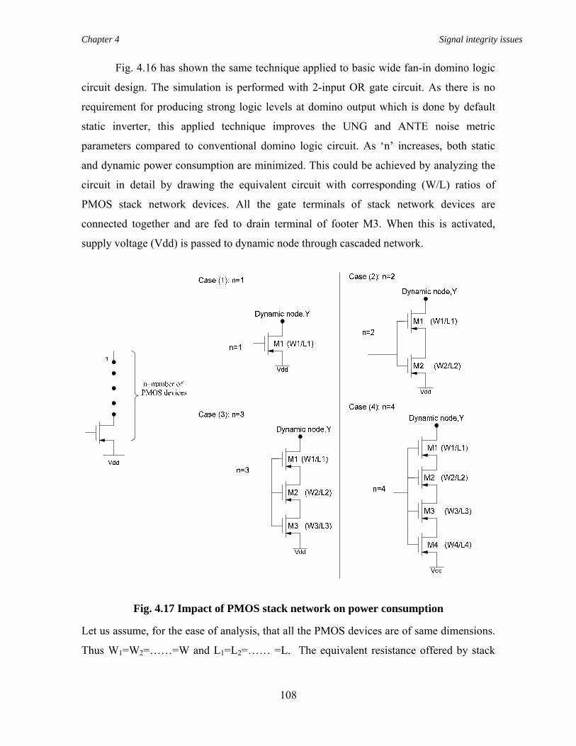
Chapter 4 Signal integrity issues
108
Fig. 4.16 has shown the same technique applied to basic wide fan-in domino logic
circuit design. The simulation is performed with 2-input OR gate circuit. As there is no
requirement for producing strong logic levels at domino output which is done by default
static inverter, this applied technique improves the UNG and ANTE noise metric
parameters compared to conventional domino logic circuit. As ‘n’ increases, both static
and dynamic power consumption are minimized. This could be achieved by analyzing the
circuit in detail by drawing the equivalent circuit with corresponding (W/L) ratios of
PMOS stack network devices. All the gate terminals of stack network devices are
connected together and are fed to drain terminal of footer M3. When this is activated,
supply voltage (Vdd) is passed to dynamic node through cascaded network.
Fig. 4.17 Impact of PMOS stack network on power consumption
Let us assume, for the ease of analysis, that all the PMOS devices are of same dimensions.
Thus W1=W2=……=W and L1=L2=…… =L. The equivalent resistance offered by stack
Chapter 4 Signal integrity issues
109
network is calculated individually in all the cases and corresponding power consumption is
formulated.
Case (1): n=1
The equivalent WL
⎛ ⎞⎜ ⎟⎝ ⎠
ratio is1
1
WL⎛ ⎞⎜ ⎟⎝ ⎠
.
PDynamic =
2
eRdynamic
quivalent
V, where eR quivalent α
1
1
1WL
⎛ ⎞⎜ ⎟⎝ ⎠
Since (W1=W2=……) =W and (L1=L2=……) =L
eR quivalent = K. 1
1
1WL
⎛ ⎞⎜ ⎟⎝ ⎠
= K. 1WL
⎛ ⎞⎜ ⎟⎝ ⎠
= R1 [ where K is a constant]
Therefore, PDynamic =1
2VR
=P1 (Let us say)
Case (2): n=2
The equivalent WL
⎛ ⎞⎜ ⎟⎝ ⎠
ratio is effective of {series connected 1
1
WL⎛ ⎞⎜ ⎟⎝ ⎠
and2
2
WL⎛ ⎞⎜ ⎟⎝ ⎠
}
1 2
1 2
( )W or WL L
⎛ ⎞⎜ ⎟+⎝ ⎠
PDynamic =
2
eRdynamic
quivalent
V
Since (W1=W2=……) =W and (L1=L2=……) =L
eR quivalent = K. 1 2
1 2
1( )W or W
L L⎛ ⎞⎜ ⎟+⎝ ⎠
= K. 1
2WL
⎛ ⎞⎜ ⎟⎝ ⎠
= R2
Therefore, PDynamic =2
2
VR
=P2.
Chapter 4 Signal integrity issues
110
The width of series connected transistors remains unchanged and channel length increases
since channel length of each transistor is added to that of other transistor and as a result the
total length will be summation of all individual channel lengths.
Thus, clearly R2 > R1 and P2 < P1.
Case (3): n=3
The equivalent WL
⎛ ⎞⎜ ⎟⎝ ⎠
ratio is effective of {series connected1
1
WL⎛ ⎞⎜ ⎟⎝ ⎠
,2
2
WL⎛ ⎞⎜ ⎟⎝ ⎠
and3
3
WL⎛ ⎞⎜ ⎟⎝ ⎠
}
1 2 3
1 2 3
( ) ( )W or W or WL L L
⎛ ⎞⎜ ⎟+ +⎝ ⎠
PDynamic =
2
eRdynamic
quivalent
V
Since (W1=W2=……) =W and (L1=L2=……) =L
eR quivalent = K. 1 2 3
1 2 3
1( ) ( )W or W or WL L L
⎛ ⎞⎜ ⎟+ +⎝ ⎠
= K. 1
3WL
⎛ ⎞⎜ ⎟⎝ ⎠
= R3
Therefore, PDynamic =2
3
VR
=P3.
Clearly R3 > R2 > R1 and thus P3 < P2 < P1.
Case (4): n=4
The equivalent WL
⎛ ⎞⎜ ⎟⎝ ⎠
ratio is effective of {series connected1
1
WL⎛ ⎞⎜ ⎟⎝ ⎠
,2
2
WL⎛ ⎞⎜ ⎟⎝ ⎠
,3
3
WL⎛ ⎞⎜ ⎟⎝ ⎠
and4
4
WL⎛ ⎞⎜ ⎟⎝ ⎠
}
1 2 3 4
1 2 3 4
( ) ( ) ( )W or W or W or WL L L L
⎛ ⎞⎜ ⎟+ + +⎝ ⎠
PDynamic =
2
eRdynamic
quivalent
V
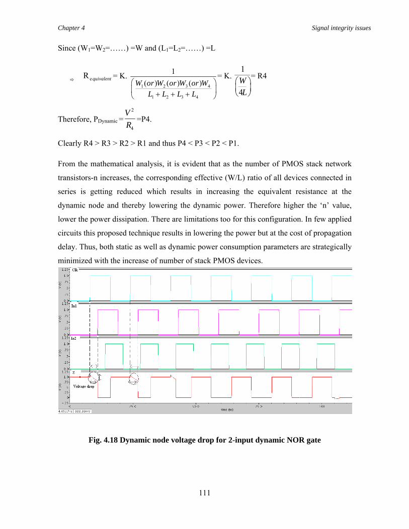
Chapter 4 Signal integrity issues
111
Since (W1=W2=……) =W and (L1=L2=……) =L
eR quivalent = K. 1 2 3 4
1 2 3 4
1( ) ( ) ( )W or W or W or W
L L L L⎛ ⎞⎜ ⎟+ + +⎝ ⎠
= K. 1
4WL
⎛ ⎞⎜ ⎟⎝ ⎠
= R4
Therefore, PDynamic =2
4
VR
=P4.
Clearly R4 > R3 > R2 > R1 and thus P4 < P3 < P2 < P1.
From the mathematical analysis, it is evident that as the number of PMOS stack network
transistors-n increases, the corresponding effective (W/L) ratio of all devices connected in
series is getting reduced which results in increasing the equivalent resistance at the
dynamic node and thereby lowering the dynamic power. Therefore higher the ‘n’ value,
lower the power dissipation. There are limitations too for this configuration. In few applied
circuits this proposed technique results in lowering the power but at the cost of propagation
delay. Thus, both static as well as dynamic power consumption parameters are strategically
minimized with the increase of number of stack PMOS devices.
Fig. 4.18 Dynamic node voltage drop for 2-input dynamic NOR gate
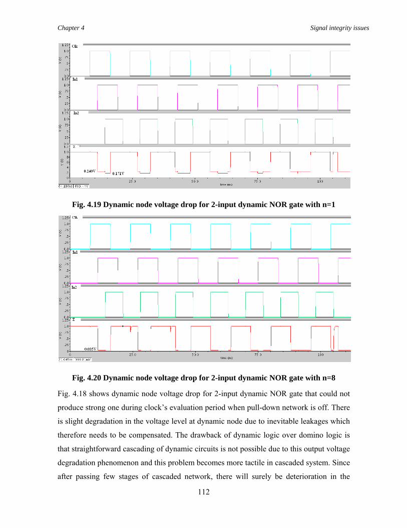
Chapter 4 Signal integrity issues
112
Fig. 4.19 Dynamic node voltage drop for 2-input dynamic NOR gate with n=1
Fig. 4.20 Dynamic node voltage drop for 2-input dynamic NOR gate with n=8
Fig. 4.18 shows dynamic node voltage drop for 2-input dynamic NOR gate that could not
produce strong one during clock’s evaluation period when pull-down network is off. There
is slight degradation in the voltage level at dynamic node due to inevitable leakages which
therefore needs to be compensated. The drawback of dynamic logic over domino logic is
that straightforward cascading of dynamic circuits is not possible due to this output voltage
degradation phenomenon and this problem becomes more tactile in cascaded system. Since
after passing few stages of cascaded network, there will surely be deterioration in the
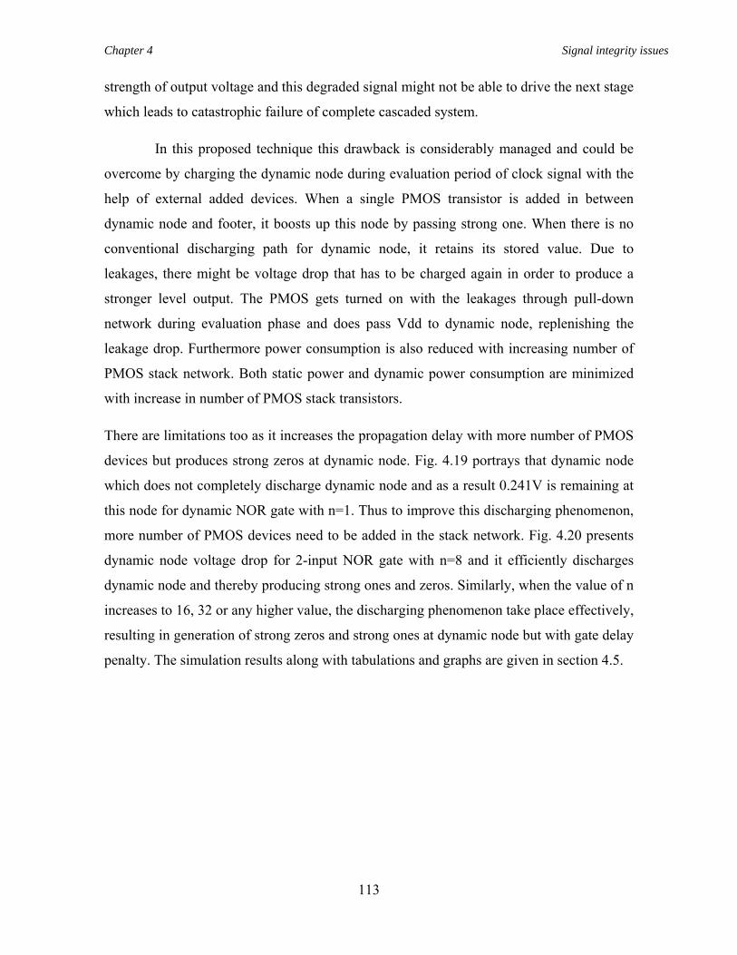
Chapter 4 Signal integrity issues
113
strength of output voltage and this degraded signal might not be able to drive the next stage
which leads to catastrophic failure of complete cascaded system.
In this proposed technique this drawback is considerably managed and could be
overcome by charging the dynamic node during evaluation period of clock signal with the
help of external added devices. When a single PMOS transistor is added in between
dynamic node and footer, it boosts up this node by passing strong one. When there is no
conventional discharging path for dynamic node, it retains its stored value. Due to
leakages, there might be voltage drop that has to be charged again in order to produce a
stronger level output. The PMOS gets turned on with the leakages through pull-down
network during evaluation phase and does pass Vdd to dynamic node, replenishing the
leakage drop. Furthermore power consumption is also reduced with increasing number of
PMOS stack network. Both static power and dynamic power consumption are minimized
with increase in number of PMOS stack transistors.
There are limitations too as it increases the propagation delay with more number of PMOS
devices but produces strong zeros at dynamic node. Fig. 4.19 portrays that dynamic node
which does not completely discharge dynamic node and as a result 0.241V is remaining at
this node for dynamic NOR gate with n=1. Thus to improve this discharging phenomenon,
more number of PMOS devices need to be added in the stack network. Fig. 4.20 presents
dynamic node voltage drop for 2-input NOR gate with n=8 and it efficiently discharges
dynamic node and thereby producing strong ones and zeros. Similarly, when the value of n
increases to 16, 32 or any higher value, the discharging phenomenon take place effectively,
resulting in generation of strong zeros and strong ones at dynamic node but with gate delay
penalty. The simulation results along with tabulations and graphs are given in section 4.5.
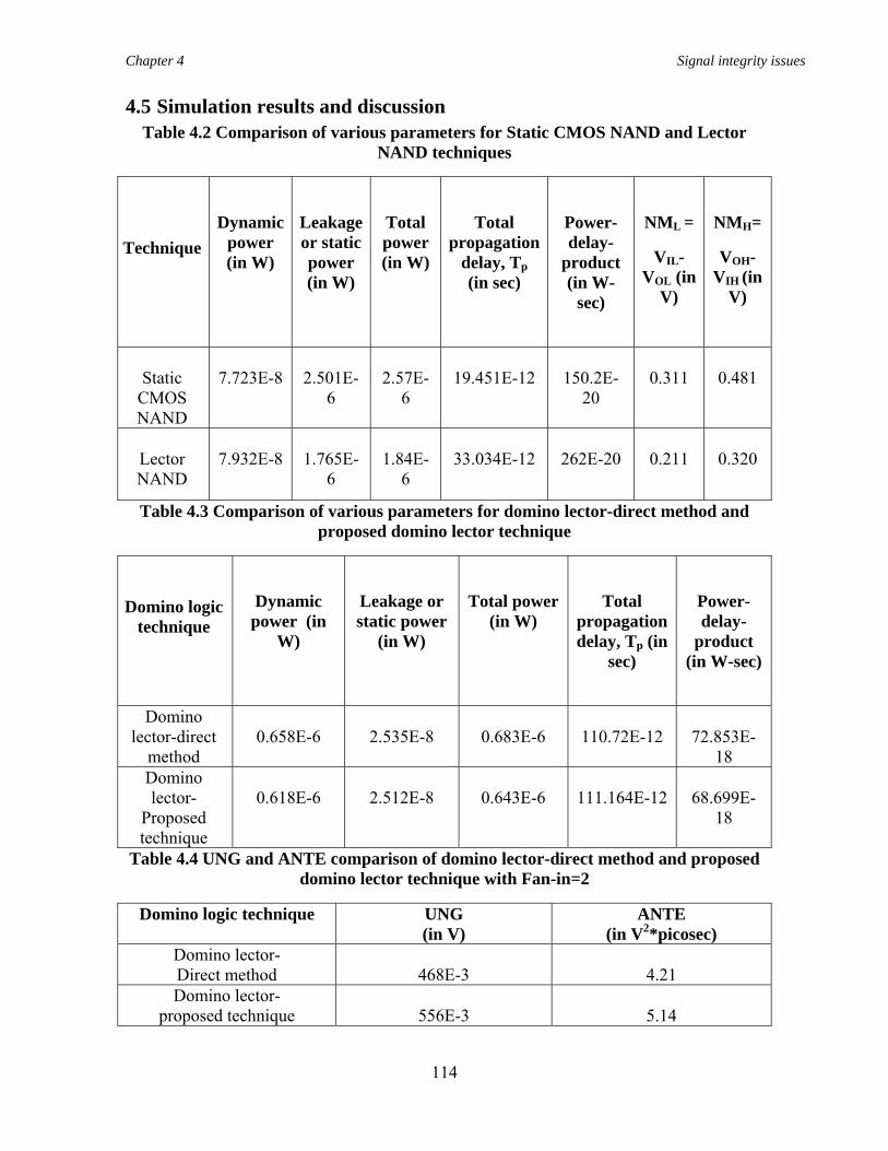
Chapter 4 Signal integrity issues
114
4.5 Simulation results and discussion Table 4.2 Comparison of various parameters for Static CMOS NAND and Lector
NAND techniques
Technique
Dynamic power (in W)
Leakage or static power (in W)
Total power (in W)
Total propagation
delay, Tp (in sec)
Power-delay-
product (in W-
sec)
NML =
VIL-VOL (in
V)
NMH=
VOH-VIH (in
V)
Static
CMOS NAND
7.723E-8
2.501E-
6
2.57E-
6
19.451E-12
150.2E-
20
0.311
0.481
Lector NAND
7.932E-8
1.765E-
6
1.84E-
6
33.034E-12
262E-20
0.211
0.320
Table 4.3 Comparison of various parameters for domino lector-direct method and proposed domino lector technique
Domino logic technique
Dynamic power (in
W)
Leakage or static power
(in W)
Total power (in W)
Total propagation delay, Tp (in
sec)
Power-delay-
product (in W-sec)
Domino
lector-direct method
0.658E-6
2.535E-8
0.683E-6
110.72E-12
72.853E-
18 Domino lector-
Proposed technique
0.618E-6
2.512E-8
0.643E-6
111.164E-12
68.699E-
18
Table 4.4 UNG and ANTE comparison of domino lector-direct method and proposed domino lector technique with Fan-in=2
Domino logic technique UNG (in V)
ANTE (in V2*picosec)
Domino lector- Direct method
468E-3
4.21
Domino lector- proposed technique
556E-3
5.14
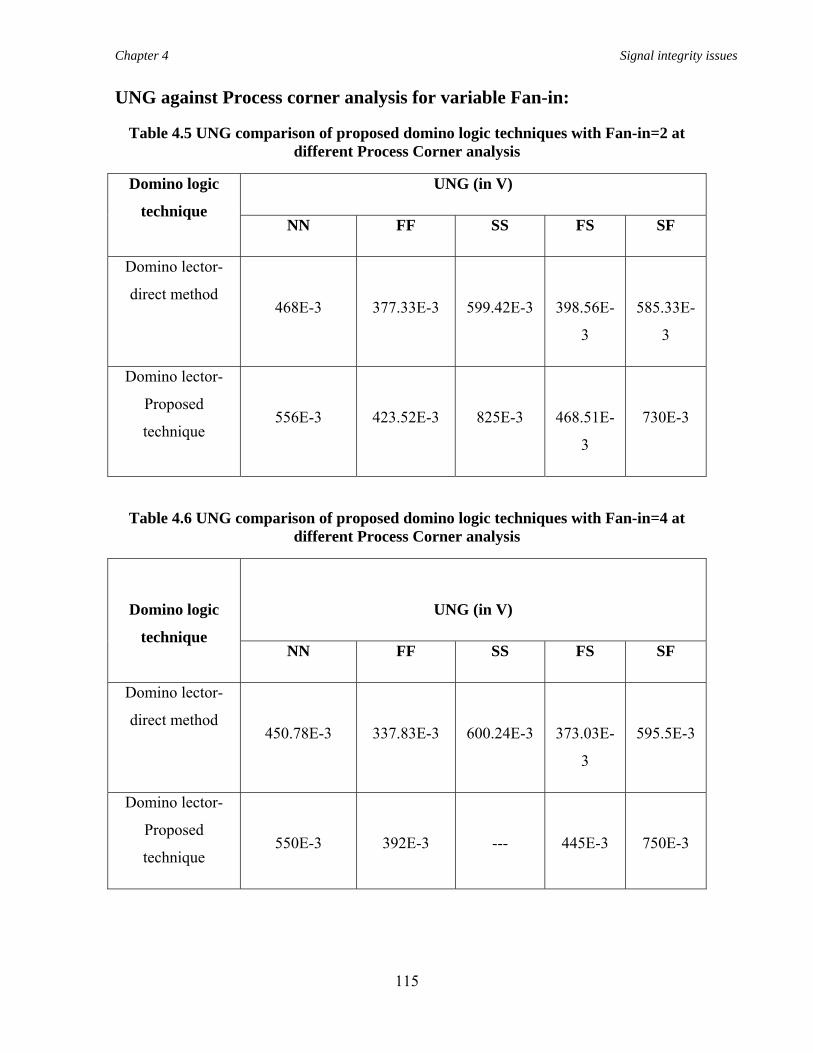
Chapter 4 Signal integrity issues
115
UNG against Process corner analysis for variable Fan-in:
Table 4.5 UNG comparison of proposed domino logic techniques with Fan-in=2 at different Process Corner analysis
Domino logic
technique
UNG (in V)
NN FF SS FS SF
Domino lector-
direct method
468E-3
377.33E-3
599.42E-3
398.56E-
3
585.33E-
3
Domino lector-
Proposed
technique
556E-3
423.52E-3
825E-3
468.51E-
3
730E-3
Table 4.6 UNG comparison of proposed domino logic techniques with Fan-in=4 at different Process Corner analysis
Domino logic
technique
UNG (in V)
NN FF SS FS SF
Domino lector-
direct method
450.78E-3
337.83E-3
600.24E-3
373.03E-
3
595.5E-3
Domino lector-
Proposed
technique
550E-3
392E-3
---
445E-3
750E-3
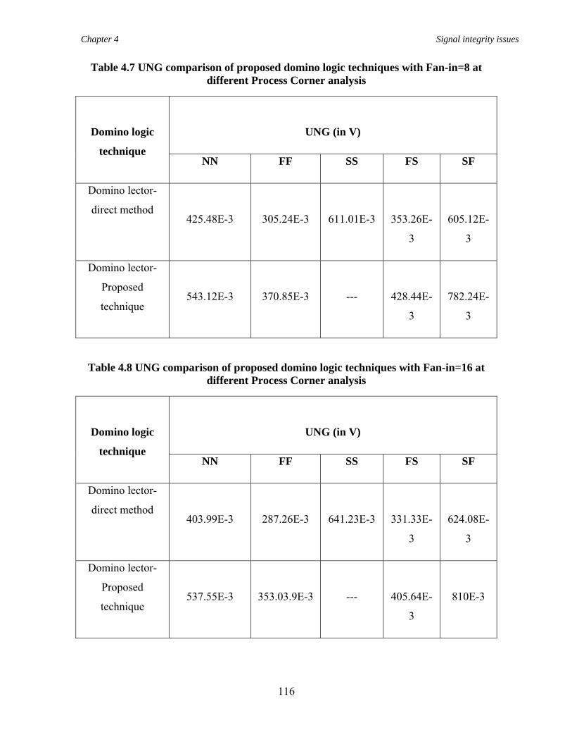
Chapter 4 Signal integrity issues
116
Table 4.7 UNG comparison of proposed domino logic techniques with Fan-in=8 at different Process Corner analysis
Domino logic
technique
UNG (in V)
NN FF SS FS SF
Domino lector-
direct method
425.48E-3
305.24E-3
611.01E-3
353.26E-
3
605.12E-
3
Domino lector-
Proposed
technique
543.12E-3
370.85E-3
---
428.44E-
3
782.24E-
3
Table 4.8 UNG comparison of proposed domino logic techniques with Fan-in=16 at different Process Corner analysis
Domino logic
technique
UNG (in V)
NN FF SS FS SF
Domino lector-
direct method
403.99E-3
287.26E-3
641.23E-3
331.33E-
3
624.08E-
3
Domino lector-
Proposed
technique
537.55E-3
353.03.9E-3
---
405.64E-
3
810E-3
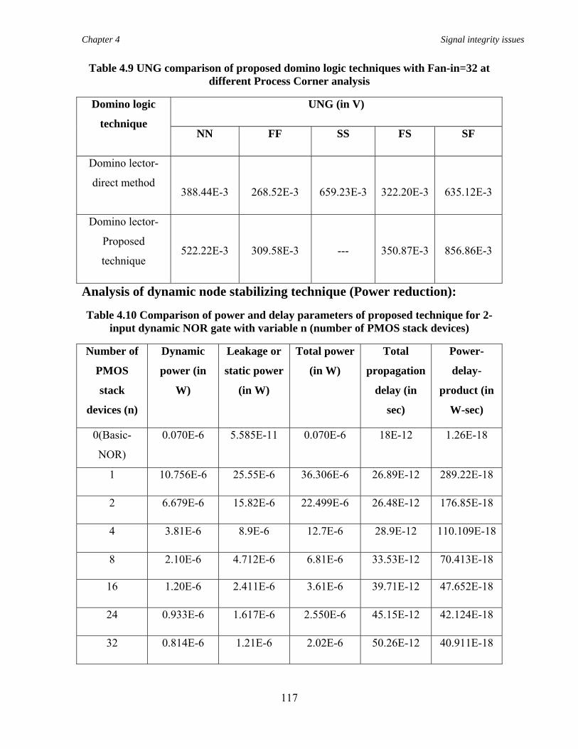
Chapter 4 Signal integrity issues
117
Table 4.9 UNG comparison of proposed domino logic techniques with Fan-in=32 at different Process Corner analysis
Domino logic
technique
UNG (in V)
NN FF SS FS SF
Domino lector-
direct method
388.44E-3
268.52E-3
659.23E-3
322.20E-3
635.12E-3
Domino lector-
Proposed
technique
522.22E-3
309.58E-3
---
350.87E-3
856.86E-3
Analysis of dynamic node stabilizing technique (Power reduction):
Table 4.10 Comparison of power and delay parameters of proposed technique for 2-input dynamic NOR gate with variable n (number of PMOS stack devices)
Number of
PMOS
stack
devices (n)
Dynamic
power (in
W)
Leakage or
static power
(in W)
Total power
(in W)
Total
propagation
delay (in
sec)
Power-
delay-
product (in
W-sec)
0(Basic-
NOR)
0.070E-6 5.585E-11 0.070E-6 18E-12 1.26E-18
1 10.756E-6 25.55E-6 36.306E-6 26.89E-12 289.22E-18
2 6.679E-6 15.82E-6 22.499E-6 26.48E-12 176.85E-18
4 3.81E-6 8.9E-6 12.7E-6 28.9E-12 110.109E-18
8 2.10E-6 4.712E-6 6.81E-6 33.53E-12 70.413E-18
16 1.20E-6 2.411E-6 3.61E-6 39.71E-12 47.652E-18
24 0.933E-6 1.617E-6 2.550E-6 45.15E-12 42.124E-18
32 0.814E-6 1.21E-6 2.02E-6 50.26E-12 40.911E-18

Chapter 4 Signal integrity issues
118
Table 4.11 Comparison of power and delay parameters of proposed technique for 2-input domino OR gate with variable n (number of PMOS stack devices)
Number of
PMOS stack
devices (n)
Dynamic
power (in W)
Leakage or
static power
(in W)
Total power
(in W)
Total
propagation
delay (in sec)
Power-delay-
product (in
W-sec)
0(Basic-OR) 0.203E-6 2.75E-8 0.23E-6 47.24E-12 9.589E-18
1 11.94E-6 28.96E-6 40.90E-6 51.21E-12 611.44E-18
2 6.984E-6 16.595E-6 23.579E-6 51.29E-12 358.20E-18
4 4.00E-6 9.518E-6 13.51E-6 54.19E-12 216.76E-18
8 2.291E-6 4.403E-6 6.694E-6 59E-12 135.16E-18
16 1.43E-6 2.311E-6 3.74E-6 66.75E-12 95.45E-18
24 1.214E-6 1.655E-6 2.869E-6 72.78E-12 88.35E-18
32 1.152E-6 1.245E-6 2.397E-6 78.27E-12 90.16E-18
Table 4.12 UNG and ANTE comparison of proposed technique applied for domino 2-input OR gate for various stack devices
Number of stack PMOS
devices (n)
UNG (in V) ANTE (in V2*picoSec)
0 402.5E-3 3.58
1 923E-3 8.91
2 770.3E-3 7.22
4 670.75E-3 6.38
8 638E-3 5.84
16 632.5E-3 5.63
24 629E-3 5.53
32 625E-3 5.41
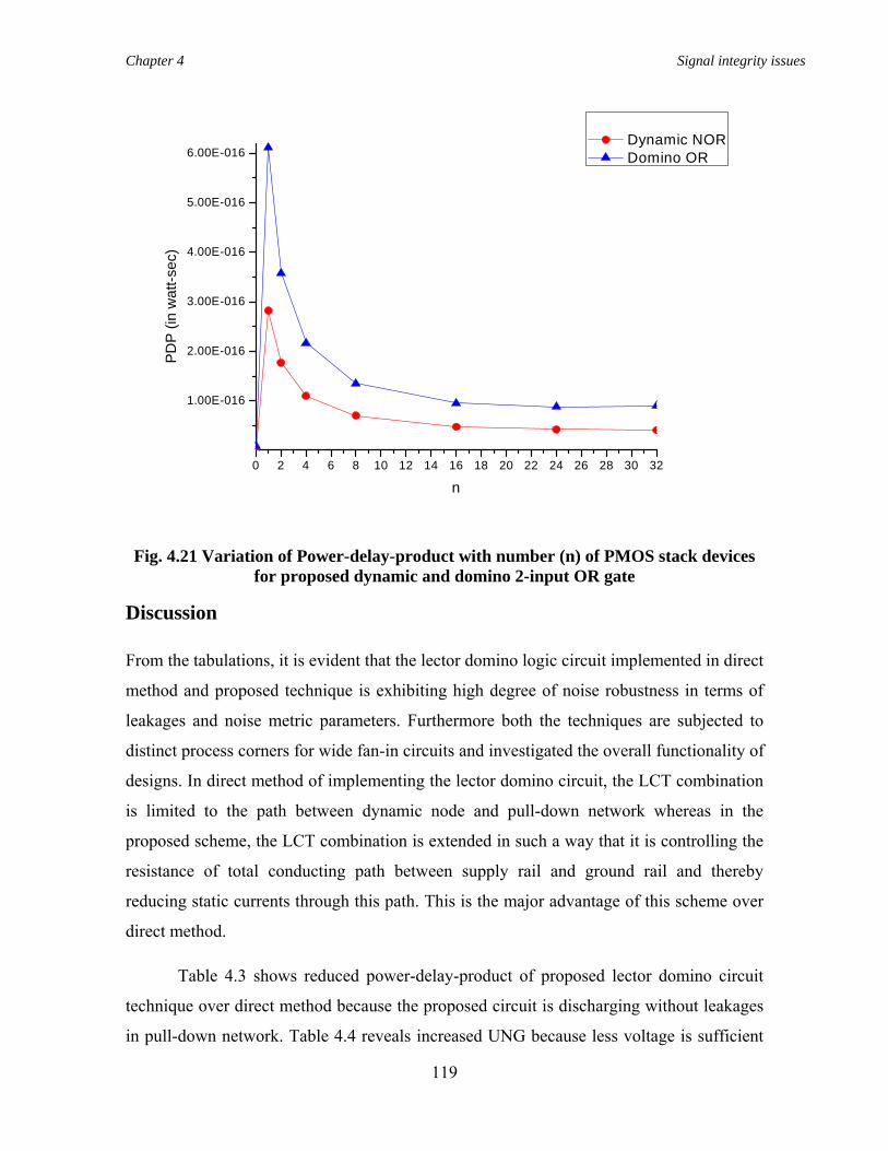
Chapter 4 Signal integrity issues
119
0 2 4 6 8 10 12 14 16 18 20 22 24 26 28 30 32
1.00E-016
2.00E-016
3.00E-016
4.00E-016
5.00E-016
6.00E-016P
DP
(in
wat
t-sec
)
n
Dynamic NOR Domino OR
Fig. 4.21 Variation of Power-delay-product with number (n) of PMOS stack devices for proposed dynamic and domino 2-input OR gate
Discussion
From the tabulations, it is evident that the lector domino logic circuit implemented in direct
method and proposed technique is exhibiting high degree of noise robustness in terms of
leakages and noise metric parameters. Furthermore both the techniques are subjected to
distinct process corners for wide fan-in circuits and investigated the overall functionality of
designs. In direct method of implementing the lector domino circuit, the LCT combination
is limited to the path between dynamic node and pull-down network whereas in the
proposed scheme, the LCT combination is extended in such a way that it is controlling the
resistance of total conducting path between supply rail and ground rail and thereby
reducing static currents through this path. This is the major advantage of this scheme over
direct method.
Table 4.3 shows reduced power-delay-product of proposed lector domino circuit
technique over direct method because the proposed circuit is discharging without leakages
in pull-down network. Table 4.4 reveals increased UNG because less voltage is sufficient
Chapter 4 Signal integrity issues
120
to turn a single NMOS in pull-down network. As fan-in increases, more voltage is required
to make the evaluation network on which results in reduction of the noise gain.
Analyzing the process-corner analysis, amongst five typical corners (NN, SS, FF,
FS and SF), Normal-Normal corner is providing nominal switching threshold voltages for
NMOS and PMOS devices as specified by EDA tool. Generally, all the designed circuits
will operate as per design specifications and according to user constraints at NN corner.
Thus evaluation and estimation of overall performance of designed circuit by subjecting at
NN process corner alone does not finish the task. In fact the circuit is required to be tested
by subjecting at all the extreme corners. Having done that entire task, then only the
performance of circuit can be judged. Always the SS corner is assuring increased noise
tolerance and which is also observed from tabulations. Highest UNG is recorded in SS
corner since both NMOS and PMOS transistors are slow running devices which implied
that their switching threshold voltages are high. Thus, the circuit is made less sensitive to
noise glitches and hence the nature of being responsive to gate input noise glitches is
gradually reducing, that in turn increases UNG. So, in comparison with other process
corners, SS corner always exhibits highest UNG. Also in SF corner, as NMOS switching
threshold voltage is higher and PMOS switching threshold voltage is lower, it also
contributes increment in noise gain but not as efficient as SS corner because the PMOS
threshold voltage is responding to noise impulses at gate inputs which makes the circuit
more sensitive to noise glitches. Normally, in comparison with NN, FS and FF corners,
circuit at SF corner exhibits better immunity towards noise. At FF process corner, both
NMOS and PMOS devices are of very high speed with reduced switching threshold
voltages and consume more power. The least UNG is noted in FF case. This becomes more
tactile with wide fan-in circuits. With increased fan-in, the UNG in other process corners is
gradually lowering since more voltage is required to turn pull-down network on and
discharging phenomenon is becoming slow. Thus normal circuits usually become more
sensitive to noise glitches at gate inputs due to their lower threshold voltages and as a
result UNG is reduced. But proposed circuits are functioning at FF corner efficiently.
Normally, with increased fan-in, the UNG lowers. The performance of circuit at FS
process corner lies in between the corresponding performances at NN and FF corners. As
NMOS possesses lower threshold voltage, it becomes more sensitive to noise. Despite
Chapter 4 Signal integrity issues
121
slow PMOS device, the corner is lowering the noise immunity. From the tabulations, it is
evident that proposed techniques exhibit high degree of robustness at FS corner too.
The topology of LCT combination in proposed lector domino logic circuit technique
assures high noise tolerance than that of direct method. UNG measurements at various
process corners for wide fan-in circuits reveal that proposed techniques are less sensitive to
external and internal ambient noise glitches. This could be achieved by configuring the
circuit with series connected transistors, in the path between supply rail and ground rail,
called stack effect. This possesses the conducting path wherein more than one transistor is
off between supply rail and ground rail which is less leaky than that of only a single
transistor is off. Lector scheme introduced two leakage control transistors as described in
such a way that one of them is at cut-off region.
Having analyzed the results from process corner analysis, it is clear that proposed
circuit techniques assure high noise robustness with increased fan-in despite few
limitations at various corners. Proposed techniques are functioning efficiently, at all the
corners for lower fan-in circuits but with increased fan-in, the operating region of design
has started becoming limited to few corners only which might be due to the reason that the
circuits are being operated at lower bias voltage of 1V. For example, from the simulations,
it is clear that the UNG is getting lowered at NN, FF and FS process corners for higher fan-
in. Thus increasing the bias voltage range would facilitate broadening the operating region
of proposed domino techniques at all the process corners for wide fan-in circuits but while
doing so the power consumption must be taken care off as it is directly proportional to
square of supply voltage. Hence optimization through trade-off between supply voltage
and process corners is necessary while improving the proposed domino logic circuit
techniques.
The proposed technique for stabilizing dynamic node also operates efficiently and
is able to energize the dynamic node effectively. As the number of PMOS stack devices is
increasing, the power consumption is less and more stronger values (strong one) are being
generated by circuit at dynamic node. This can be observed from Fig. 4.21. It is also noted
from the simulations that both static current and dynamic current are being limited and as a
Chapter 4 Signal integrity issues
122
result total power consumption is minimized with more number of PMOS stack devices.
Despite these benefits, proposed technique suffers from increased propagation delay.
Table 4.9 and 4.10 reveal that proposed technique for stabilizing dynamic node is
assuring high performance from the perspectives of dynamic power, leakage power,
propagation delay and PDP. With increased stack PMOS devices, the equivalent resistance
of stack network is increasing and as result the power consumption is lowered. But the
main disadvantage is that, the complete discharging phenomenon is not occurring since
small amount of voltage is remaining at dynamic node which is due to increased PMOS
devices in stack network and as result discharging process is becoming slow and in-
effective. It is evident from Table 4.11 that, UNG and ANTE metric parameters are
reducing with increased stack PMOS devices and when compared with conventional
domino OR gate circuit, proposed technique assures higher noise tolerance.
Fig. 4.16 has shown the same technique applied to basic domino logic design. The
simulation is performed with 2-input OR gate circuit. As there is no requirement for
producing strong logic levels at domino output which is done by default static inverter, this
applied technique improves the UNG and ANTE noise metric parameters compared to
conventional domino logic circuit. As ‘n’ increases, both static and dynamic power
consumption are minimized. This could be achieved by analyzing the circuit in detail by
drawing the equivalent circuit with corresponding (W/L) ratios of PMOS stack network
devices.
4.6 Conclusion Therefore this chapter in section-1 gives general introduction to need for power reduction
and leakage minimization. Section 4.2 discussed signal integrity issues in detail with
simulations. Section 4.3 described the prior works related to leakage power reduction
schemes and the lector technique. Modified lector domino scheme and dynamic node
stabilizing technique are proposed in section 4.4. Simulation results along with discussion
are presented in section 4.5.
All the simulations are done at CMOS 90 nm process technology with 1 V power
supply. The proposed domino logic circuit techniques are simulated at distinct ambient
conditions by subjecting them to various process corners and thereby observations are
Chapter 4 Signal integrity issues
123
tabulated. Comparisons are made and conclusions are drawn. Noise analysis is carried out
which includes the need for robustness, various metric parameters for measuring noise
immunity or robustness of domino circuits such as UNG, ANTE along with the method of
calculations, various sources of noise in domino logic circuits and their role on operating
region.
Process corner analysis and various corners involved in it along with their
significant role on the overall functionality of the designed lector domino logic circuit are
described. Also the consequences of subjecting the device to the extreme corners with the
boundary limitations are discussed.
The result section shows the calculations and comparisons of all the parameters of
proposed lector domino techniques. The primary design parameters such dynamic power,
leakage or static power, total power, PDP (power-delay-product), UNG and ANTE for
various fan-in circuits of existing and proposed techniques are measured. The comparisons
along with tabulations are made and discussed the functionality with pros and cons.
Thus the proposed circuits are exhibiting improved leakage reduction and greater noise
immunity.
Chapter 5 Domino Schmitt Trigger Circuits
125
CHAPTER 5 DESIGN OF VARIOUS DOMINO BASED SCHMITT
TRIGGER CIRCUITS
5.1 Introduction Schmitt trigger (ST) is a comparator based application circuit that possesses hysteresis.
This can be obtained by implementing positive feedback to the non-inverting differential
amplifier. Also it is an active circuit which converts analog input data into digital output.
The name “trigger” is given to this active circuit since output or the final response is
triggered or actively driven by corresponding change at the input signal and hence it is
referred as ‘Schmitt trigger’. The output of Schmitt trigger remains unchanged or retains
its previously stored value until the input changes through some threshold point. This
Schmitt trigger circuit was first invented by the U.S scientist named Otto. H. Schmitt in the
year 1934 [5-20]. The peculiar phenomenon of Schmitt trigger circuit is that it exhibits
‘hysteresis’ behavior which is bounded by two typical threshold values called upper
threshold point and lower threshold point. Hysteresis also acts as memory state. Thus, if
the input is crossing the upper threshold value, then it triggers the output and according to
that output reaches logic high. On the other hand, if the input is below lower threshold
value, then the corresponding change drives output and hence it becomes logic low. As it
possesses two threshold points, there is a chance of getting a state wherein the input lies in
between upper threshold value and lower threshold value. Therefore, if this case arises then
the output retains its value and implies that the previous data is stored by the design when
input lies in between two threshold values. This peculiar dual threshold phenomenon is
called hysteresis. It also implies that the Schmitt trigger functions as a memory storage
device as a bi-stable circuit (typical basic latch or flip-flop circuit) since two stable states
are being stored by this design in this hysteresis mode. Schmitt trigger can be constructed
by using latch and vice-versa.
In this chapter Schmitt trigger is designed using domino logic circuit techniques by
applying the proposed circuit techniques and is simulated. It is observed that the Schmitt
trigger possesses various hysteresis phenomena with different techniques applied.
In this chapter, we propose a novel leakage power reduction domino Schmitt trigger
circuits. The rest of the chapter is organized as follows. Section 5.2 explains conventional
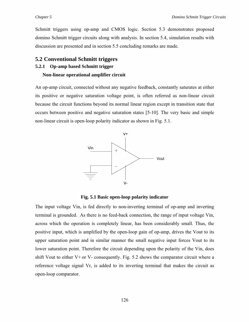
Chapter 5 Domino Schmitt Trigger Circuits
126
Schmitt triggers using op-amp and CMOS logic. Section 5.3 demonstrates proposed
domino Schmitt trigger circuits along with analysis. In section 5.4, simulation results with
discussion are presented and in section 5.5 concluding remarks are made.
5.2 Conventional Schmitt triggers 5.2.1 Op-amp based Schmitt trigger
Non-linear operational amplifier circuit
An op-amp circuit, connected without any negative feedback, constantly saturates at either
its positive or negative saturation voltage point, is often referred as non-linear circuit
because the circuit functions beyond its normal linear region except in transition state that
occurs between positive and negative saturation states [5-10]. The very basic and simple
non-linear circuit is open-loop polarity indicator as shown in Fig. 5.1.
Fig. 5.1 Basic open-loop polarity indicator
The input voltage Vin, is fed directly to non-inverting terminal of op-amp and inverting
terminal is grounded. As there is no feed-back connection, the range of input voltage Vin,
across which the operation is completely linear, has been considerably small. Thus, the
positive input, which is amplified by the open-loop gain of op-amp, drives the Vout to its
upper saturation point and in similar manner the small negative input forces Vout to its
lower saturation point. Therefore the circuit depending upon the polarity of the Vin, does
shift Vout to either V+ or V- consequently. Fig. 5.2 shows the comparator circuit where a
reference voltage signal Vr, is added to its inverting terminal that makes the circuit as
open-loop comparator.
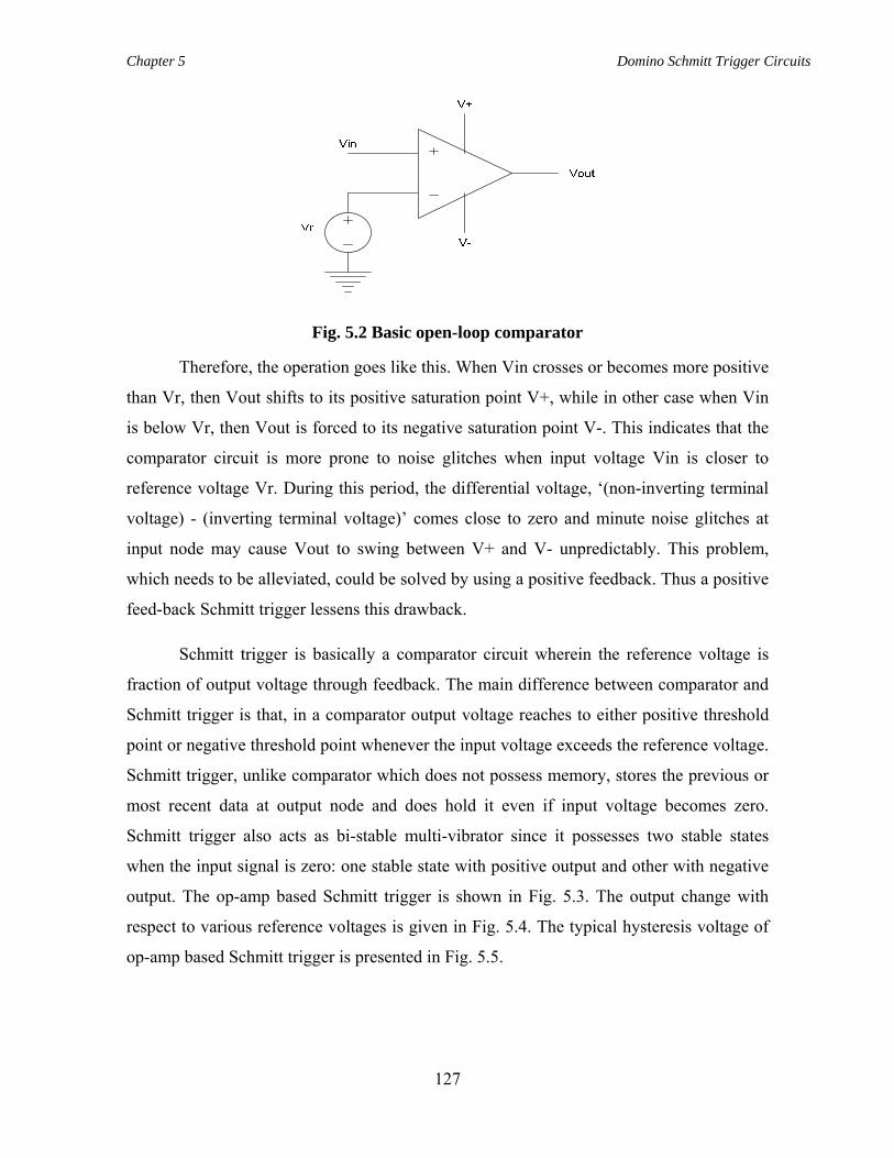
Chapter 5 Domino Schmitt Trigger Circuits
127
Fig. 5.2 Basic open-loop comparator
Therefore, the operation goes like this. When Vin crosses or becomes more positive
than Vr, then Vout shifts to its positive saturation point V+, while in other case when Vin
is below Vr, then Vout is forced to its negative saturation point V-. This indicates that the
comparator circuit is more prone to noise glitches when input voltage Vin is closer to
reference voltage Vr. During this period, the differential voltage, ‘(non-inverting terminal
voltage) - (inverting terminal voltage)’ comes close to zero and minute noise glitches at
input node may cause Vout to swing between V+ and V- unpredictably. This problem,
which needs to be alleviated, could be solved by using a positive feedback. Thus a positive
feed-back Schmitt trigger lessens this drawback.
Schmitt trigger is basically a comparator circuit wherein the reference voltage is
fraction of output voltage through feedback. The main difference between comparator and
Schmitt trigger is that, in a comparator output voltage reaches to either positive threshold
point or negative threshold point whenever the input voltage exceeds the reference voltage.
Schmitt trigger, unlike comparator which does not possess memory, stores the previous or
most recent data at output node and does hold it even if input voltage becomes zero.
Schmitt trigger also acts as bi-stable multi-vibrator since it possesses two stable states
when the input signal is zero: one stable state with positive output and other with negative
output. The op-amp based Schmitt trigger is shown in Fig. 5.3. The output change with
respect to various reference voltages is given in Fig. 5.4. The typical hysteresis voltage of
op-amp based Schmitt trigger is presented in Fig. 5.5.
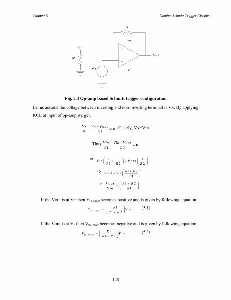
Chapter 5 Domino Schmitt Trigger Circuits
128
Fig. 5.3 Op-amp based Schmitt trigger configuration
Let us assume the voltage between inverting and non-inverting terminal is Vx. By applying
KCL at input of op-amp we get,
01 2
Vx Vx VoutR R
−+ = . Clearly, Vx=Vin.
Thus 01 2
Vin Vin VoutR R
−+ =
1 1 11 2 2
V in V o u tR R R
⎛ ⎞ ⎛ ⎞+ =⎜ ⎟ ⎜ ⎟⎝ ⎠ ⎝ ⎠
1 21
R RV out V inR+⎛ ⎞= ⎜ ⎟
⎝ ⎠
1 21
V o u t R RV in R
+⎛ ⎞= ⎜ ⎟⎝ ⎠
If the Vout is at V+ then Vth-upper becomes positive and is given by following equation.1
1 2th u p p e rR V
R RV −
⎛ ⎞= +⎜ ⎟+⎝ ⎠ (5.1)
If the Vout is at V- then Vth-lower becomes negative and is given by following equation.1
1 2th lo w e rR V
R RV −
⎛ ⎞= −⎜ ⎟+⎝ ⎠ (5.2)
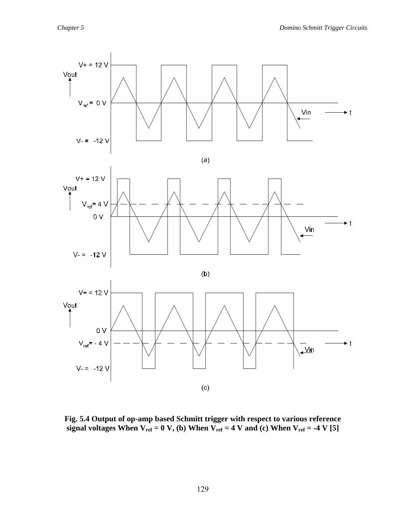
Chapter 5 Domino Schmitt Trigger Circuits
129
Fig. 5.4 Output of op-amp based Schmitt trigger with respect to various reference signal voltages When Vref = 0 V, (b) When Vref = 4 V and (c) When Vref = -4 V [5]
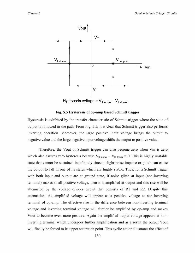
Chapter 5 Domino Schmitt Trigger Circuits
130
Fig. 5.5 Hysteresis of op-amp based Schmitt trigger
Hysteresis is exhibited by the transfer characteristic of Schmitt trigger where the state of
output is followed in the path. From Fig. 5.5, it is clear that Schmitt trigger also performs
inverting operation. Moreover, the large positive input voltage brings the output to
negative value and the large negative input voltage shifts the output to positive value.
Therefore, the Vout of Schmitt trigger can also become zero when Vin is zero
which also assures zero hysteresis because Vth-upper – Vth-lower = 0. This is highly unstable
state that cannot be sustained indefinitely since a slight noise impulse or glitch can cause
the output to fall in one of its states which are highly stable. Thus, for a Schmitt trigger
with both input and output are at ground state, if noise glitch at input (non-inverting
terminal) makes small positive voltage, then it is amplified at output and this rise will be
attenuated by the voltage divider circuit that consists of R1 and R2. Despite this
attenuation, the amplified voltage will appear as a positive voltage at non-inverting
terminal of op-amp. The effective rise in the difference between non-inverting terminal
voltage and inverting terminal voltage will further be amplified by op-amp and makes
Vout to become even more positive. Again the amplified output voltage appears at non-
inverting terminal which undergoes further amplification and as a result the output Vout
will finally be forced to its upper saturation point. This cyclic action illustrates the effect of
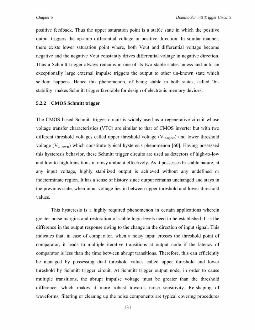
Chapter 5 Domino Schmitt Trigger Circuits
131
positive feedback. Thus the upper saturation point is a stable state in which the positive
output triggers the op-amp differential voltage in positive direction. In similar manner,
there exists lower saturation point where, both Vout and differential voltage become
negative and the negative Vout constantly drives differential voltage in negative direction.
Thus a Schmitt trigger always remains in one of its two stable states unless and until an
exceptionally large external impulse triggers the output to other un-known state which
seldom happens. Hence this phenomenon, of being stable in both states, called ‘bi-
stability’ makes Schmitt trigger favorable for design of electronic memory devices.
5.2.2 CMOS Schmitt trigger
The CMOS based Schmitt trigger circuit is widely used as a regenerative circuit whose
voltage transfer characteristics (VTC) are similar to that of CMOS inverter but with two
different threshold voltages called upper threshold voltage (Vth-upper) and lower threshold
voltage (Vth-lower) which constitute typical hysteresis phenomenon [60]. Having possessed
this hysteresis behavior, these Schmitt trigger circuits are used as detectors of high-to-low
and low-to-high transitions in noisy ambient effectively. As it possesses bi-stable nature, at
any input voltage, highly stabilized output is achieved without any undefined or
indeterminate region. It has a sense of history since output remains unchanged and stays in
the previous state, when input voltage lies in between upper threshold and lower threshold
values.
This hysteresis is a highly required phenomenon in certain applications wherein
greater noise margins and restoration of stable logic levels need to be established. It is the
difference in the output response owing to the change in the direction of input signal. This
indicates that, in case of comparator, when a noisy input crosses the threshold point of
comparator, it leads to multiple iterative transitions at output node if the latency of
comparator is less than the time between abrupt transitions. Therefore, this can efficiently
be managed by possessing dual threshold values called upper threshold and lower
threshold by Schmitt trigger circuit. At Schmitt trigger output node, in order to cause
multiple transitions, the abrupt impulse voltage must be greater than the threshold
difference, which makes it more robust towards noise sensitivity. Re-shaping of
waveforms, filtering or cleaning up the noise components are typical covering procedures
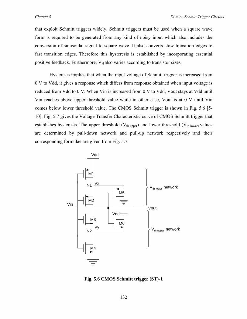
Chapter 5 Domino Schmitt Trigger Circuits
132
that exploit Schmitt triggers widely. Schmitt triggers must be used when a square wave
form is required to be generated from any kind of noisy input which also includes the
conversion of sinusoidal signal to square wave. It also converts slow transition edges to
fast transition edges. Therefore this hysteresis is established by incorporating essential
positive feedback. Furthermore, VH also varies according to transistor sizes.
Hysteresis implies that when the input voltage of Schmitt trigger is increased from
0 V to Vdd, it gives a response which differs from response obtained when input voltage is
reduced from Vdd to 0 V. When Vin is increased from 0 V to Vdd, Vout stays at Vdd until
Vin reaches above upper threshold value while in other case, Vout is at 0 V until Vin
comes below lower threshold value. The CMOS Schmitt trigger is shown in Fig. 5.6 [5-
10]. Fig. 5.7 gives the Voltage Transfer Characteristic curve of CMOS Schmitt trigger that
establishes hysteresis. The upper threshold (Vth-upper) and lower threshold (Vth-lower) values
are determined by pull-down network and pull-up network respectively and their
corresponding formulae are given from Fig. 5.7.
M1
M2
M3
M4
Vdd
Vdd
M5
M6
Vin
VxN1
N2Vy
Vout
Vth-lower network
Vth-upper network
Fig. 5.6 CMOS Schmitt trigger (ST)-1
Chapter 5 Domino Schmitt Trigger Circuits
133
Fig. 5.7 Voltage Transfer Characteristic (VTC) curve of CMOS Schmitt trigger-1
From the VTC, it is clear that Vth-lower < Vth-upper and Hysteresis voltage (VH) = Vth-upper -
Vth-lower.
Vout = Vdd when Vin < Vth-upper,
= 0 when Vin > Vth-upper.
Similarly, Vout = 0 when Vin > Vth-lower,
= Vdd when Vin < Vth-lower.
When (Vth-lower < Vin < Vth-upper), then Vout = Vout-previous (previous data/history).
Transistors M1, M2 and M5 determine lower threshold voltage and devices M3, M4 and
M6 establish upper threshold voltage. M3 and M4 are in series combination and Vin drives
both of them. When Vin = 0 then Vout=Vdd and M6 is turned on and it acts as feedback
path from supply rail. As long as Vin is increasing, M6 keeps M3 off even after M4 turns
on. The mathematical expression for Vth-upper is given below.
46
416
th upper
Vdd tnV
Vββ
ββ
−
⎛ ⎞+ ⎜ ⎟⎝ ⎠=⎛ ⎞
+ ⎜ ⎟⎝ ⎠
, where 46ββ is the beta ratio of M4 and M6 devices
respectively.
Beta calculation: The drain current equation of N-MOSFET is given below.
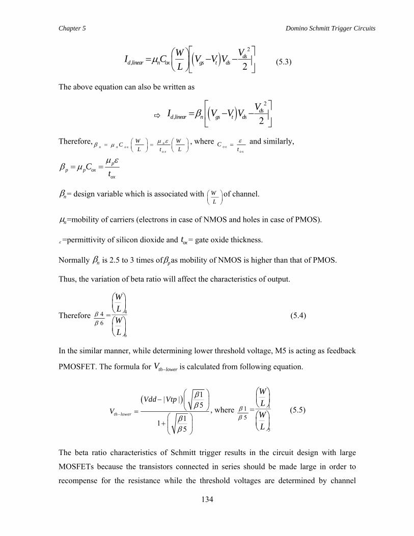
Chapter 5 Domino Schmitt Trigger Circuits
134
( )2
, 2ds
d linear n ox gs t dsVWI C V V V
Lμ
⎡ ⎤⎛ ⎞= − −⎢ ⎥⎜ ⎟⎝ ⎠⎣ ⎦
(5.3)
The above equation can also be written as
( )2
, 2ds
d linear n gs t dsVI V V Vβ
⎡ ⎤= − −⎢ ⎥
⎣ ⎦
Therefore, nn n o x
o x
W WCL t L
μ εβ μ ⎛ ⎞ ⎛ ⎞= =⎜ ⎟ ⎜ ⎟⎝ ⎠ ⎝ ⎠
, where o x
o x
Ctε
= and similarly,
pp p ox
ox
Ctμ ε
β μ= =
nβ = design variable which is associated with WL
⎛ ⎞⎜ ⎟⎝ ⎠
of channel.
nμ =mobility of carriers (electrons in case of NMOS and holes in case of PMOS).
ε =permittivity of silicon dioxide and oxt = gate oxide thickness.
Normally nβ is 2.5 to 3 times of pβ as mobility of NMOS is higher than that of PMOS.
Thus, the variation of beta ratio will affect the characteristics of output.
Therefore 46
ββ
= 4
6
WLWL
⎛ ⎞⎜ ⎟⎝ ⎠⎛ ⎞⎜ ⎟⎝ ⎠
(5.4)
In the similar manner, while determining lower threshold voltage, M5 is acting as feedback
PMOSFET. The formula for th lowerV − is calculated from following equation.
( ) 1| |5
115
th lower
Vdd VtpV
ββ
ββ
−
⎛ ⎞− ⎜ ⎟
⎝ ⎠=⎛ ⎞
+ ⎜ ⎟⎝ ⎠
, where 15
ββ
= 1
5
WLWL
⎛ ⎞⎜ ⎟⎝ ⎠⎛ ⎞⎜ ⎟⎝ ⎠
(5.5)
The beta ratio characteristics of Schmitt trigger results in the circuit design with large
MOSFETs because the transistors connected in series should be made large in order to
recompense for the resistance while the threshold voltages are determined by channel
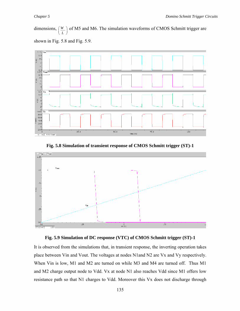
Chapter 5 Domino Schmitt Trigger Circuits
135
dimensions, WL
⎛ ⎞⎜ ⎟⎝ ⎠
of M5 and M6. The simulation waveforms of CMOS Schmitt trigger are
shown in Fig. 5.8 and Fig. 5.9.
Fig. 5.8 Simulation of transient response of CMOS Schmitt trigger (ST)-1
Fig. 5.9 Simulation of DC response (VTC) of CMOS Schmitt trigger (ST)-1
It is observed from the simulations that, in transient response, the inverting operation takes
place between Vin and Vout. The voltages at nodes N1and N2 are Vx and Vy respectively.
When Vin is low, M1 and M2 are turned on while M3 and M4 are turned off. Thus M1
and M2 charge output node to Vdd. Vx at node N1 also reaches Vdd since M1 offers low
resistance path so that N1 charges to Vdd. Moreover this Vx does not discharge through
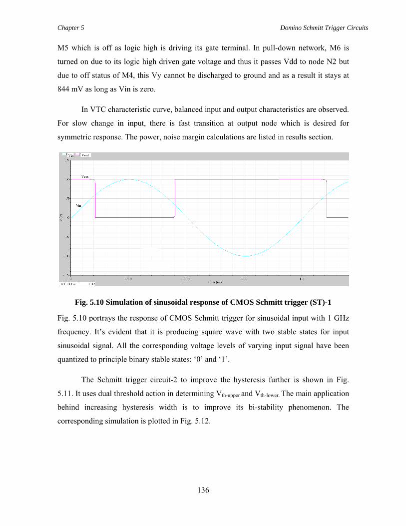
Chapter 5 Domino Schmitt Trigger Circuits
136
M5 which is off as logic high is driving its gate terminal. In pull-down network, M6 is
turned on due to its logic high driven gate voltage and thus it passes Vdd to node N2 but
due to off status of M4, this Vy cannot be discharged to ground and as a result it stays at
844 mV as long as Vin is zero.
In VTC characteristic curve, balanced input and output characteristics are observed.
For slow change in input, there is fast transition at output node which is desired for
symmetric response. The power, noise margin calculations are listed in results section.
Fig. 5.10 Simulation of sinusoidal response of CMOS Schmitt trigger (ST)-1
Fig. 5.10 portrays the response of CMOS Schmitt trigger for sinusoidal input with 1 GHz
frequency. It’s evident that it is producing square wave with two stable states for input
sinusoidal signal. All the corresponding voltage levels of varying input signal have been
quantized to principle binary stable states: ‘0’ and ‘1’.
The Schmitt trigger circuit-2 to improve the hysteresis further is shown in Fig.
5.11. It uses dual threshold action in determining Vth-upper and Vth-lower. The main application
behind increasing hysteresis width is to improve its bi-stability phenomenon. The
corresponding simulation is plotted in Fig. 5.12.
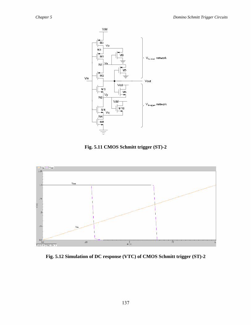
Chapter 5 Domino Schmitt Trigger Circuits
137
Fig. 5.11 CMOS Schmitt trigger (ST)-2
Fig. 5.12 Simulation of DC response (VTC) of CMOS Schmitt trigger (ST)-2
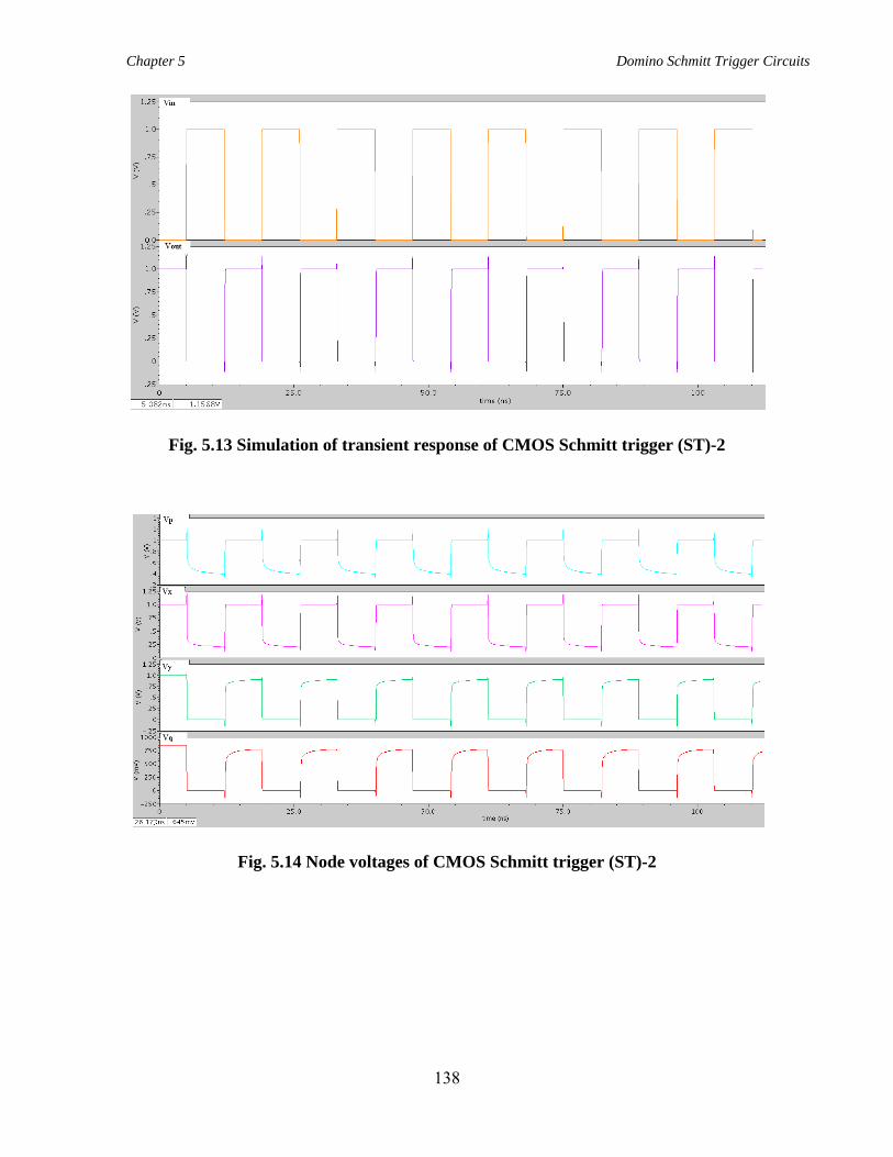
Chapter 5 Domino Schmitt Trigger Circuits
138
Fig. 5.13 Simulation of transient response of CMOS Schmitt trigger (ST)-2
Fig. 5.14 Node voltages of CMOS Schmitt trigger (ST)-2
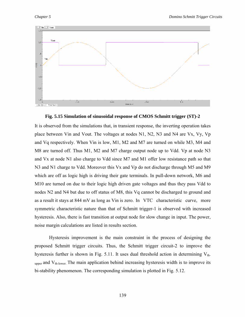
Chapter 5 Domino Schmitt Trigger Circuits
139
Fig. 5.15 Simulation of sinusoidal response of CMOS Schmitt trigger (ST)-2
It is observed from the simulations that, in transient response, the inverting operation takes
place between Vin and Vout. The voltages at nodes N1, N2, N3 and N4 are Vx, Vy, Vp
and Vq respectively. When Vin is low, M1, M2 and M7 are turned on while M3, M4 and
M8 are turned off. Thus M1, M2 and M7 charge output node up to Vdd. Vp at node N3
and Vx at node N1 also charge to Vdd since M7 and M1 offer low resistance path so that
N3 and N1 charge to Vdd. Moreover this Vx and Vp do not discharge through M5 and M9
which are off as logic high is driving their gate terminals. In pull-down network, M6 and
M10 are turned on due to their logic high driven gate voltages and thus they pass Vdd to
nodes N2 and N4 but due to off status of M8, this Vq cannot be discharged to ground and
as a result it stays at 844 mV as long as Vin is zero. In VTC characteristic curve, more
symmetric characteristic nature than that of Schmitt trigger-1 is observed with increased
hysteresis. Also, there is fast transition at output node for slow change in input. The power,
noise margin calculations are listed in results section.
Hysteresis improvement is the main constraint in the process of designing the
proposed Schmitt trigger circuits. Thus, the Schmitt trigger circuit-2 to improve the
hysteresis further is shown in Fig. 5.11. It uses dual threshold action in determining Vth-
upper and Vth-lower. The main application behind increasing hysteresis width is to improve its
bi-stability phenomenon. The corresponding simulation is plotted in Fig. 5.12.
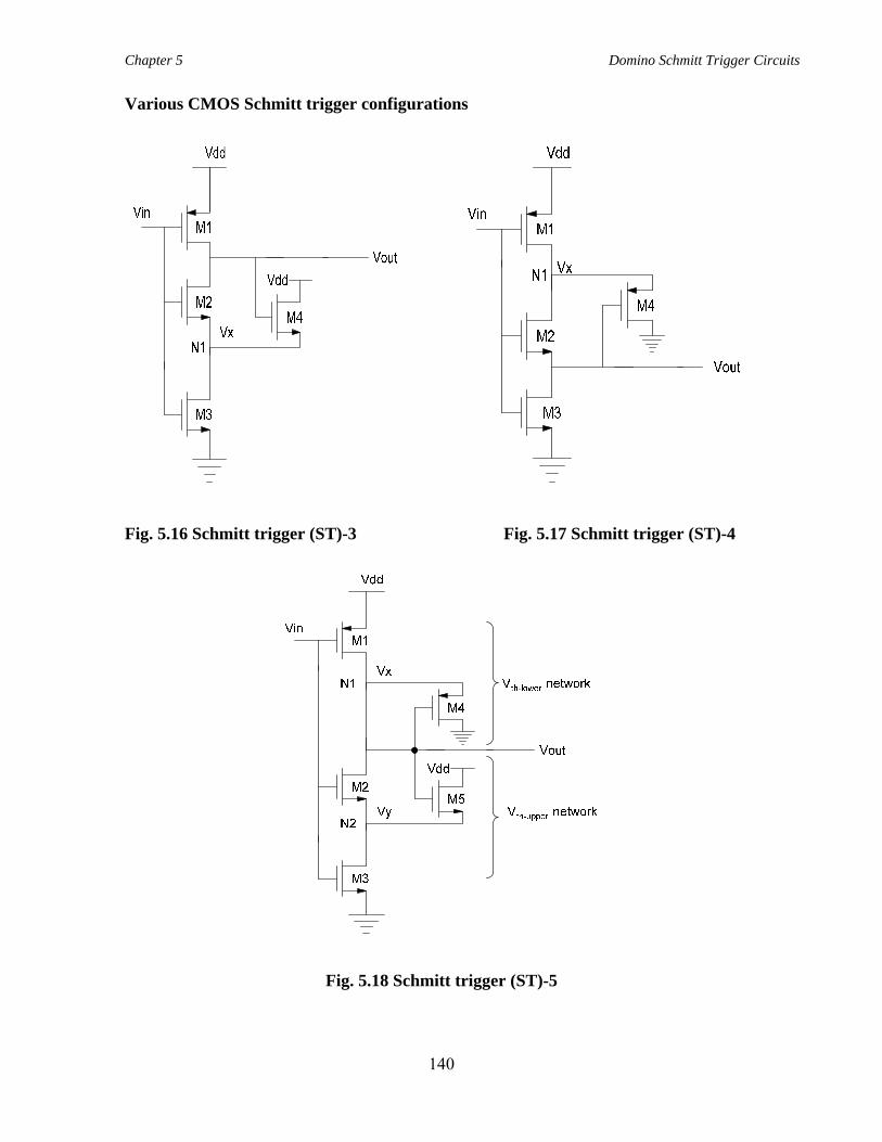
Chapter 5 Domino Schmitt Trigger Circuits
140
Various CMOS Schmitt trigger configurations
Fig. 5.16 Schmitt trigger (ST)-3 Fig. 5.17 Schmitt trigger (ST)-4
Fig. 5.18 Schmitt trigger (ST)-5
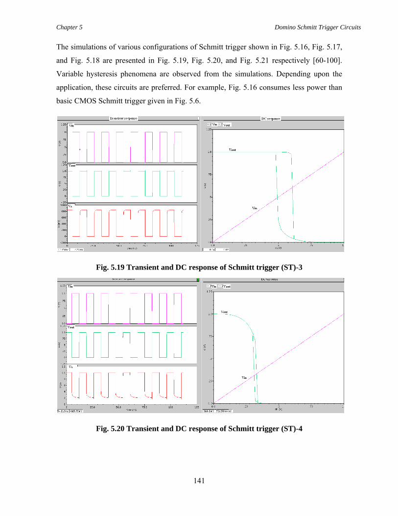
Chapter 5 Domino Schmitt Trigger Circuits
141
The simulations of various configurations of Schmitt trigger shown in Fig. 5.16, Fig. 5.17,
and Fig. 5.18 are presented in Fig. 5.19, Fig. 5.20, and Fig. 5.21 respectively [60-100].
Variable hysteresis phenomena are observed from the simulations. Depending upon the
application, these circuits are preferred. For example, Fig. 5.16 consumes less power than
basic CMOS Schmitt trigger given in Fig. 5.6.
Fig. 5.19 Transient and DC response of Schmitt trigger (ST)-3
Fig. 5.20 Transient and DC response of Schmitt trigger (ST)-4
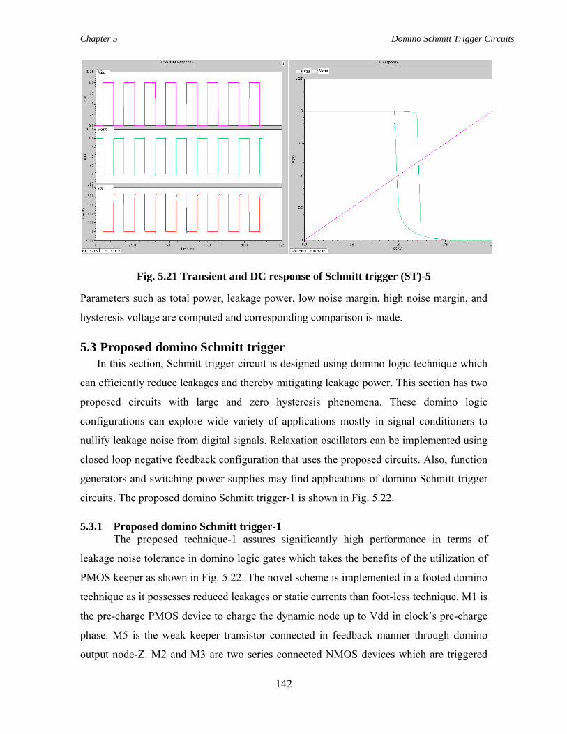
Chapter 5 Domino Schmitt Trigger Circuits
142
Fig. 5.21 Transient and DC response of Schmitt trigger (ST)-5
Parameters such as total power, leakage power, low noise margin, high noise margin, and
hysteresis voltage are computed and corresponding comparison is made.
5.3 Proposed domino Schmitt trigger In this section, Schmitt trigger circuit is designed using domino logic technique which
can efficiently reduce leakages and thereby mitigating leakage power. This section has two
proposed circuits with large and zero hysteresis phenomena. These domino logic
configurations can explore wide variety of applications mostly in signal conditioners to
nullify leakage noise from digital signals. Relaxation oscillators can be implemented using
closed loop negative feedback configuration that uses the proposed circuits. Also, function
generators and switching power supplies may find applications of domino Schmitt trigger
circuits. The proposed domino Schmitt trigger-1 is shown in Fig. 5.22.
5.3.1 Proposed domino Schmitt trigger-1 The proposed technique-1 assures significantly high performance in terms of
leakage noise tolerance in domino logic gates which takes the benefits of the utilization of
PMOS keeper as shown in Fig. 5.22. The novel scheme is implemented in a footed domino
technique as it possesses reduced leakages or static currents than foot-less technique. M1 is
the pre-charge PMOS device to charge the dynamic node up to Vdd in clock’s pre-charge
phase. M5 is the weak keeper transistor connected in feedback manner through domino
output node-Z. M2 and M3 are two series connected NMOS devices which are triggered
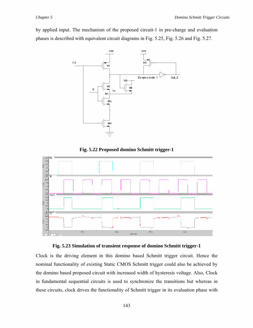
Chapter 5 Domino Schmitt Trigger Circuits
143
by applied input. The mechanism of the proposed circuit-1 in pre-charge and evaluation
phases is described with equivalent circuit diagrams in Fig. 5.25, Fig. 5.26 and Fig. 5.27.
Fig. 5.22 Proposed domino Schmitt trigger-1
Fig. 5.23 Simulation of transient response of domino Schmitt trigger-1
Clock is the driving element in this domino based Schmitt trigger circuit. Hence the
nominal functionality of existing Static CMOS Schmitt trigger could also be achieved by
the domino based proposed circuit with increased width of hysteresis voltage. Also, Clock
in fundamental sequential circuits is used to synchronize the transitions but whereas in
these circuits, clock drives the functionality of Schmitt trigger in its evaluation phase with
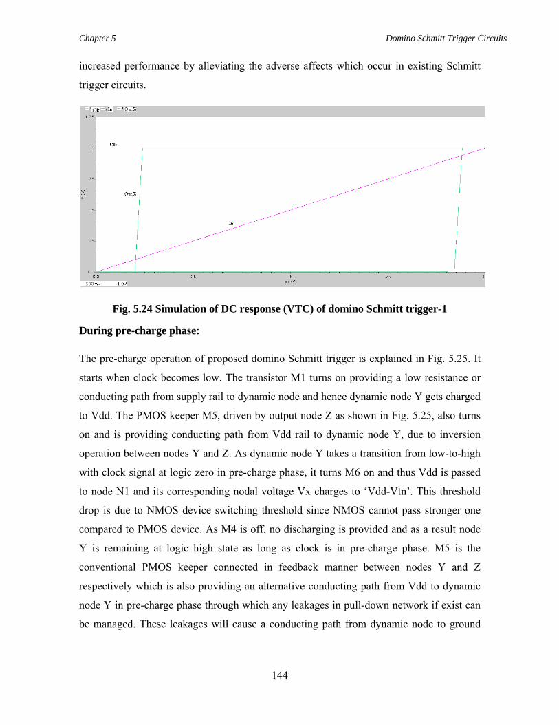
Chapter 5 Domino Schmitt Trigger Circuits
144
increased performance by alleviating the adverse affects which occur in existing Schmitt
trigger circuits.
Fig. 5.24 Simulation of DC response (VTC) of domino Schmitt trigger-1
During pre-charge phase:
The pre-charge operation of proposed domino Schmitt trigger is explained in Fig. 5.25. It
starts when clock becomes low. The transistor M1 turns on providing a low resistance or
conducting path from supply rail to dynamic node and hence dynamic node Y gets charged
to Vdd. The PMOS keeper M5, driven by output node Z as shown in Fig. 5.25, also turns
on and is providing conducting path from Vdd rail to dynamic node Y, due to inversion
operation between nodes Y and Z. As dynamic node Y takes a transition from low-to-high
with clock signal at logic zero in pre-charge phase, it turns M6 on and thus Vdd is passed
to node N1 and its corresponding nodal voltage Vx charges to ‘Vdd-Vtn’. This threshold
drop is due to NMOS device switching threshold since NMOS cannot pass stronger one
compared to PMOS device. As M4 is off, no discharging is provided and as a result node
Y is remaining at logic high state as long as clock is in pre-charge phase. M5 is the
conventional PMOS keeper connected in feedback manner between nodes Y and Z
respectively which is also providing an alternative conducting path from Vdd to dynamic
node Y in pre-charge phase through which any leakages in pull-down network if exist can
be managed. These leakages will cause a conducting path from dynamic node to ground
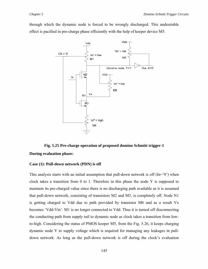
Chapter 5 Domino Schmitt Trigger Circuits
145
through which the dynamic node is forced to be wrongly discharged. This undesirable
effect is pacified in pre-charge phase efficiently with the help of keeper device M5.
Fig. 5.25 Pre-charge operation of proposed domino Schmitt trigger-1
During evaluation phase:
Case (1): Pull-down network (PDN) is off
This analysis starts with an initial assumption that pull-down network is off (In=’0’) when
clock takes a transition from 0 to 1. Therefore in this phase the node Y is supposed to
maintain its pre-charged value since there is no discharging path available as it is assumed
that pull-down network, consisting of transistors M2 and M3, is completely off. Node N1
is getting charged to Vdd due to path provided by transistor M6 and as a result Vx
becomes ‘Vdd-Vtn’. M1 is no longer connected to Vdd. Thus it is turned off disconnecting
the conducting path from supply rail to dynamic node as clock takes a transition from low-
to-high. Considering the status of PMOS keeper M5, from the Fig. 5.26, it keeps charging
dynamic node Y to supply voltage which is required for managing any leakages in pull-
down network. As long as the pull-down network is off during the clock’s evaluation
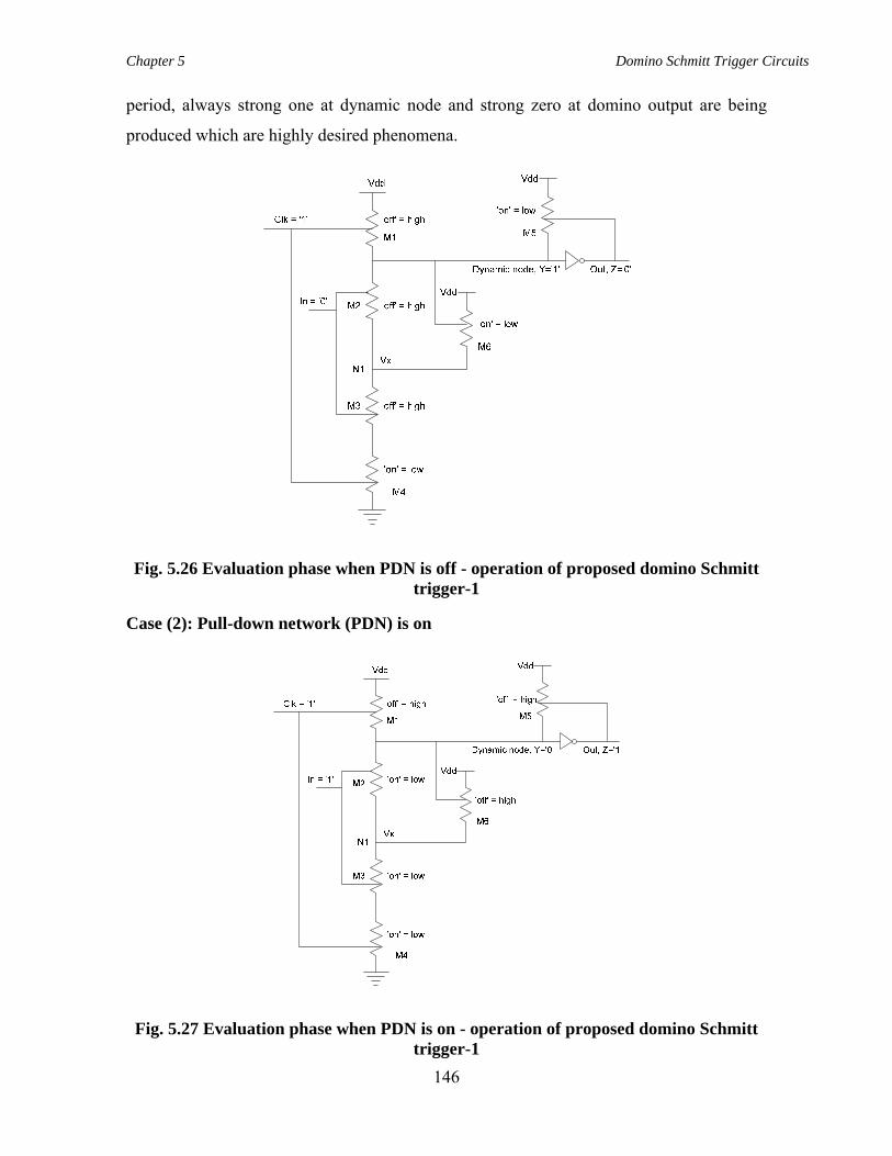
Chapter 5 Domino Schmitt Trigger Circuits
146
period, always strong one at dynamic node and strong zero at domino output are being
produced which are highly desired phenomena.
Fig. 5.26 Evaluation phase when PDN is off - operation of proposed domino Schmitt trigger-1
Case (2): Pull-down network (PDN) is on
Fig. 5.27 Evaluation phase when PDN is on - operation of proposed domino Schmitt trigger-1
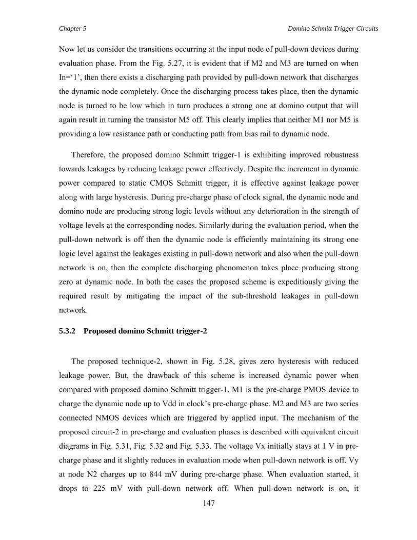
Chapter 5 Domino Schmitt Trigger Circuits
147
Now let us consider the transitions occurring at the input node of pull-down devices during
evaluation phase. From the Fig. 5.27, it is evident that if M2 and M3 are turned on when
In=‘1’, then there exists a discharging path provided by pull-down network that discharges
the dynamic node completely. Once the discharging process takes place, then the dynamic
node is turned to be low which in turn produces a strong one at domino output that will
again result in turning the transistor M5 off. This clearly implies that neither M1 nor M5 is
providing a low resistance path or conducting path from bias rail to dynamic node.
Therefore, the proposed domino Schmitt trigger-1 is exhibiting improved robustness
towards leakages by reducing leakage power effectively. Despite the increment in dynamic
power compared to static CMOS Schmitt trigger, it is effective against leakage power
along with large hysteresis. During pre-charge phase of clock signal, the dynamic node and
domino node are producing strong logic levels without any deterioration in the strength of
voltage levels at the corresponding nodes. Similarly during the evaluation period, when the
pull-down network is off then the dynamic node is efficiently maintaining its strong one
logic level against the leakages existing in pull-down network and also when the pull-down
network is on, then the complete discharging phenomenon takes place producing strong
zero at dynamic node. In both the cases the proposed scheme is expeditiously giving the
required result by mitigating the impact of the sub-threshold leakages in pull-down
network.
5.3.2 Proposed domino Schmitt trigger-2
The proposed technique-2, shown in Fig. 5.28, gives zero hysteresis with reduced
leakage power. But, the drawback of this scheme is increased dynamic power when
compared with proposed domino Schmitt trigger-1. M1 is the pre-charge PMOS device to
charge the dynamic node up to Vdd in clock’s pre-charge phase. M2 and M3 are two series
connected NMOS devices which are triggered by applied input. The mechanism of the
proposed circuit-2 in pre-charge and evaluation phases is described with equivalent circuit
diagrams in Fig. 5.31, Fig. 5.32 and Fig. 5.33. The voltage Vx initially stays at 1 V in pre-
charge phase and it slightly reduces in evaluation mode when pull-down network is off. Vy
at node N2 charges up to 844 mV during pre-charge phase. When evaluation started, it
drops to 225 mV with pull-down network off. When pull-down network is on, it
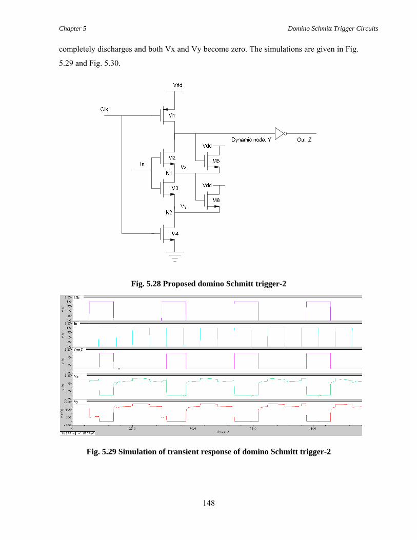
Chapter 5 Domino Schmitt Trigger Circuits
148
completely discharges and both Vx and Vy become zero. The simulations are given in Fig.
5.29 and Fig. 5.30.
Fig. 5.28 Proposed domino Schmitt trigger-2
Fig. 5.29 Simulation of transient response of domino Schmitt trigger-2
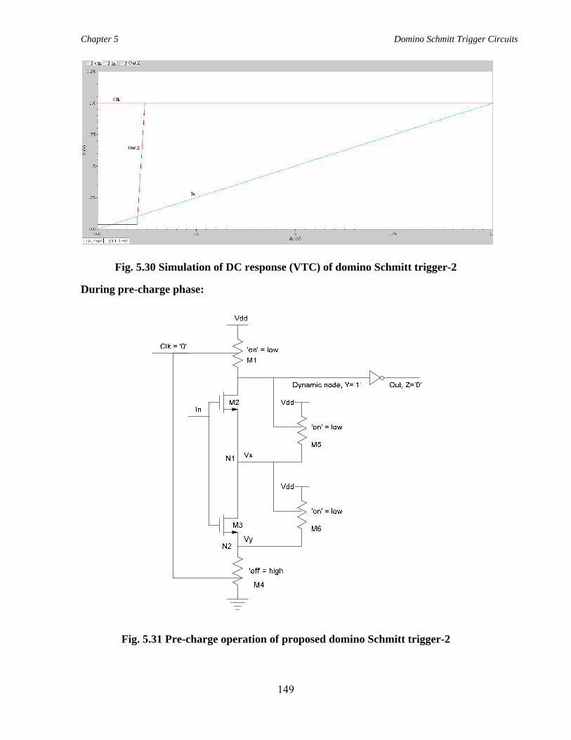
Chapter 5 Domino Schmitt Trigger Circuits
149
Fig. 5.30 Simulation of DC response (VTC) of domino Schmitt trigger-2
During pre-charge phase:
Fig. 5.31 Pre-charge operation of proposed domino Schmitt trigger-2
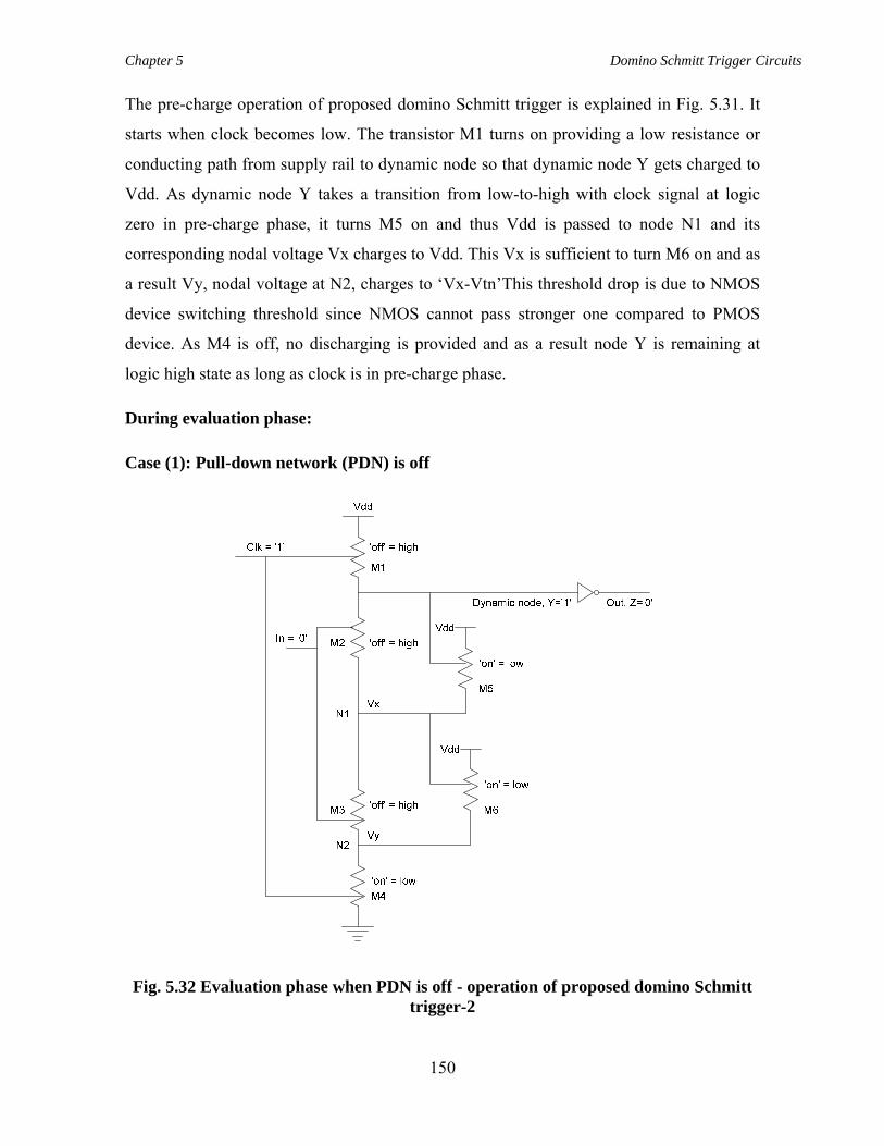
Chapter 5 Domino Schmitt Trigger Circuits
150
The pre-charge operation of proposed domino Schmitt trigger is explained in Fig. 5.31. It
starts when clock becomes low. The transistor M1 turns on providing a low resistance or
conducting path from supply rail to dynamic node so that dynamic node Y gets charged to
Vdd. As dynamic node Y takes a transition from low-to-high with clock signal at logic
zero in pre-charge phase, it turns M5 on and thus Vdd is passed to node N1 and its
corresponding nodal voltage Vx charges to Vdd. This Vx is sufficient to turn M6 on and as
a result Vy, nodal voltage at N2, charges to ‘Vx-Vtn’This threshold drop is due to NMOS
device switching threshold since NMOS cannot pass stronger one compared to PMOS
device. As M4 is off, no discharging is provided and as a result node Y is remaining at
logic high state as long as clock is in pre-charge phase.
During evaluation phase:
Case (1): Pull-down network (PDN) is off
Fig. 5.32 Evaluation phase when PDN is off - operation of proposed domino Schmitt trigger-2
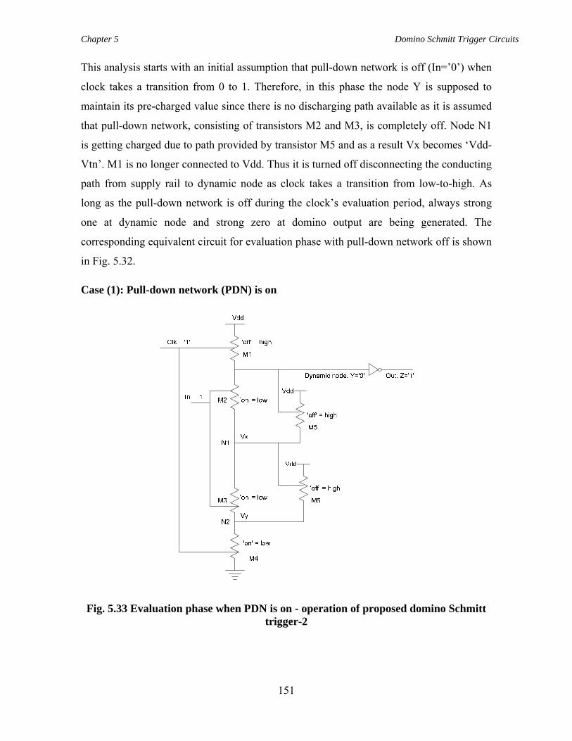
Chapter 5 Domino Schmitt Trigger Circuits
151
This analysis starts with an initial assumption that pull-down network is off (In=’0’) when
clock takes a transition from 0 to 1. Therefore, in this phase the node Y is supposed to
maintain its pre-charged value since there is no discharging path available as it is assumed
that pull-down network, consisting of transistors M2 and M3, is completely off. Node N1
is getting charged due to path provided by transistor M5 and as a result Vx becomes ‘Vdd-
Vtn’. M1 is no longer connected to Vdd. Thus it is turned off disconnecting the conducting
path from supply rail to dynamic node as clock takes a transition from low-to-high. As
long as the pull-down network is off during the clock’s evaluation period, always strong
one at dynamic node and strong zero at domino output are being generated. The
corresponding equivalent circuit for evaluation phase with pull-down network off is shown
in Fig. 5.32.
Case (1): Pull-down network (PDN) is on
Fig. 5.33 Evaluation phase when PDN is on - operation of proposed domino Schmitt trigger-2
Chapter 5 Domino Schmitt Trigger Circuits
152
From the Fig. 5.33, it is evident that if M2 and M3 are turned on when In=‘1’, then there
exists a discharging path provided by pull-down network that discharges the dynamic node
completely. Once the discharging process takes place, then the dynamic node is turned to
be low which in turn produces a strong one at domino output. Vx and Vy completely
discharge producing zero voltages at nodes N1 and N2 respectively.
Therefore, the proposed domino Schmitt trigger-2 is exhibiting improved
robustness towards leakages by reducing leakage power effectively. Despite the increment
in dynamic power compared to static proposed domino Schmitt trigger-1, it is effective
against leakage power along with zero hysteresis. During pre-charge phase of clock signal,
the dynamic node and domino node are producing strong logic levels without any
deterioration in the strength of voltage levels at the corresponding nodes. Similarly during
the evaluation period, when the pull-down network is off then the dynamic node efficiently
maintains its strong one logic level against the leakages existing in pull-down network and
also when the pull-down network is on, then the complete discharging phenomenon takes
place producing strong zero at dynamic node. In both the cases the proposed scheme is
giving the required result by minimizing sub-threshold leakages.
5.4 Results and discussion All the simulations are done in CMOS 90 nm technology with power supply 1V. Typical
parameters such as leakage power, dynamic power, propagation delay, power-delay-
product, hysteresis voltage, noise margin level and undefined region calculations are done
and comparison is made. Proposed domino Schmitt trigger circuits are exhibiting improved
performance from perspective of leakage power, hysteresis voltage and undefined region
of operation. The corresponding comparison tabulations are given below. Thus, proposed
Domino Schmitt trigger circuit design techniques assure the following benefits.
(a) Increased noise robustness,
(b) Minimized undefined region,
(c) Greater width of Hysteresis voltages and
(d) Minimized un-wanted flow of leakages.
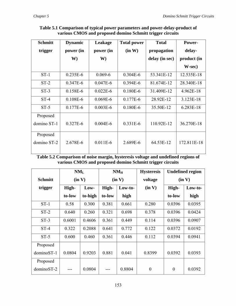
Chapter 5 Domino Schmitt Trigger Circuits
153
Table 5.1 Comparison of typical power parameters and power-delay-product of various CMOS and proposed domino Schmitt trigger circuits
Schmitt
trigger
Dynamic
power (in
W)
Leakage
power (in
W)
Total power
(in W)
Total
propagation
delay (in sec)
Power-
delay-
product (in
W-sec)
ST-1 0.235E-6 0.069-6 0.304E-6 53.341E-12 12.535E-18
ST-2 0.347E-6 0.047E-6 0.394E-6 81.674E-12 28.340E-18
ST-3 0.158E-6 0.022E-6 0.180E-6 31.409E-12 4.962E-18
ST-4 0.108E-6 0.069E-6 0.177E-6 28.92E-12 3.123E-18
ST-5 0.177E-6 0.003E-6 0.180E-6 35.50E-12 6.283E-18
Proposed
domino ST-1
0.327E-6
0.004E-6
0.331E-6
110.92E-12
36.270E-18
Proposed
domino ST-2
2.678E-6
0.011E-6
2.689E-6
64.53E-12
172.811E-18
Table 5.2 Comparison of noise margin, hysteresis voltage and undefined regions of various CMOS and proposed domino Schmitt trigger circuits
Schmitt
trigger
NML
(in V)
NMH
(in V)
Hysteresis
voltage
(in V)
Undefined region
(in V)
High-
to-low
Low-
to-high
High-
to-low
Low-to-
high
High-
to-low
Low-to-
high
ST-1 0.58 0.300 0.381 0.661 0.280 0.0396 0.0395
ST-2 0.640 0.260 0.321 0.698 0.378 0.0396 0.0424
ST-3 0.6001 0.4606 0.361 0.449 0.114 0.0396 0.0907
ST-4 0.322 0.2088 0.641 0.772 0.122 0.0372 0.0192
ST-5 0.600 0.460 0.361 0.446 0.112 0.0394 0.0941
Proposed
dominoST-1
0.0804
0.9203
0.881
0.041
0.8399
0.0392
0.0393
Proposed
dominoST-2
---
0.0804
---
0.8804
0
0
0.0392
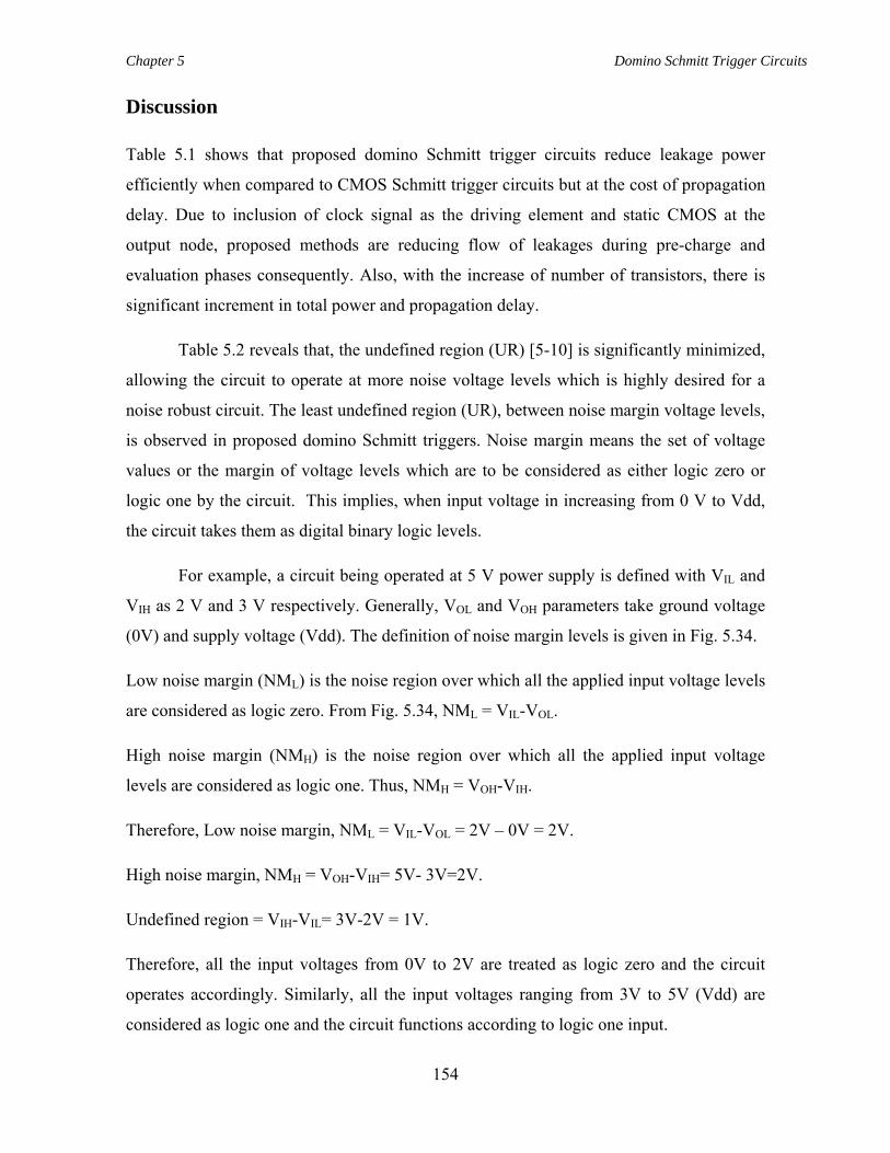
Chapter 5 Domino Schmitt Trigger Circuits
154
Discussion
Table 5.1 shows that proposed domino Schmitt trigger circuits reduce leakage power
efficiently when compared to CMOS Schmitt trigger circuits but at the cost of propagation
delay. Due to inclusion of clock signal as the driving element and static CMOS at the
output node, proposed methods are reducing flow of leakages during pre-charge and
evaluation phases consequently. Also, with the increase of number of transistors, there is
significant increment in total power and propagation delay.
Table 5.2 reveals that, the undefined region (UR) [5-10] is significantly minimized,
allowing the circuit to operate at more noise voltage levels which is highly desired for a
noise robust circuit. The least undefined region (UR), between noise margin voltage levels,
is observed in proposed domino Schmitt triggers. Noise margin means the set of voltage
values or the margin of voltage levels which are to be considered as either logic zero or
logic one by the circuit. This implies, when input voltage in increasing from 0 V to Vdd,
the circuit takes them as digital binary logic levels.
For example, a circuit being operated at 5 V power supply is defined with VIL and
VIH as 2 V and 3 V respectively. Generally, VOL and VOH parameters take ground voltage
(0V) and supply voltage (Vdd). The definition of noise margin levels is given in Fig. 5.34.
Low noise margin (NML) is the noise region over which all the applied input voltage levels
are considered as logic zero. From Fig. 5.34, NML = VIL-VOL.
High noise margin (NMH) is the noise region over which all the applied input voltage
levels are considered as logic one. Thus, NMH = VOH-VIH.
Therefore, Low noise margin, NML = VIL-VOL = 2V – 0V = 2V.
High noise margin, NMH = VOH-VIH= 5V- 3V=2V.
Undefined region = VIH-VIL= 3V-2V = 1V.
Therefore, all the input voltages from 0V to 2V are treated as logic zero and the circuit
operates accordingly. Similarly, all the input voltages ranging from 3V to 5V (Vdd) are
considered as logic one and the circuit functions according to logic one input.
Chapter 5 Domino Schmitt Trigger Circuits
155
Fig. 5.34 Noise Margin levels
Here, while increasing the input voltage from 2V to 3V, the circuit cannot respond for
these voltage levels. Since there may be a chance of getting a voltage level which is lying
in the undefined region and to which circuit does not respond as it does not understand
what kind of input has been applied at its input terminal. It leads to erroneous operation.
Hence alleviating undefined region is highly required in digital circuits by enhancing noise
margin levels. If the region between VIH and VIL is minimized, then circuit possesses
greater noise immunity. Smaller the undefined region, greater the noise immunity. This is
achieved in proposed domino Schmitt trigger circuits and the circuits are operating for all
set of input values. Apart from these, the proposed circuits exhibit various hysteresis
phenomena with improved noise immunity. The Undefined region existing between the
Noise marginal levels, VIH and VIL is also minimized which is highly desired for proper
operation of the circuit especially while working with digital logic states. This implies that
the proposed circuits provide highly stable input and output logic levels for quantization.
Therefore in these aspects the proposed circuits are better than existing ones.
5.5 Conclusion Therefore, in this chapter, we proposed domino based Schmitt trigger circuits which are
more noise tolerant than static CMOS counterpart. Leakage power is effectively minimized
in proposed circuits. Furthermore, proposed circuits can operate at all set of input voltage
levels as they possess significantly alleviated undefined regions than those of CMOS
Schmitt trigger circuits. There is increment in propagation delay and power consumption
also.

Chapter 6 Chip Tape-Out
156
CHAPTER 6 CHIP TAPE-OUT READY
6.1 Introduction Test chip is the pre-fabrication stage of VLSI design flow for bringing an electronic
chip (e-chip) form to the designed integrated circuit, which will, in next stage referred as
final fabrication stage, be sent to manufacturing section of fabrication lab in the form of
the photo mask. The basic VLSI design flow is categorized into bottom-up and top-down
approaches which are also known as back-end and front-end developments.
Bottom-up approach (back-end design):
It is a kind of development of the application which does not interact with the user directly.
It is usually built on the server based platform. Unlike front-end which can directly be
communicated by user, it interacts with server and then provides the final results or
corresponding data to user. Mechanism of back-end is little bit complex than that of front-
end.
Top-down approach (front-end design):
The name itself indicates it is on the front-line of application, which straightaway interacts
with user through an interface. It bridges the gap between the back-end environment and
front-end designer so that data is provided to user directly. Besides this, it contains many
standard libraries for mapping synthesizable designs with concerned library files.
Both the approaches converge at top-level design of VLSI design flow and continue
together towards the further steps involved in fabrication procedure. The primary steps
involved in these methods are explained in detail section 6.2. Moreover, the test chip of
proposed Schmitt trigger circuit is done in CMOS 180 nm process technology through
bottom-up approach of basic VLSI design flow. The schematic level implementation,
layout of circuit, extraction of parasitic components, transistor level simulations and other
related results are presented in section 6.3. Results are given in section 6.4 and concluding
remarks are made in section 6.5.
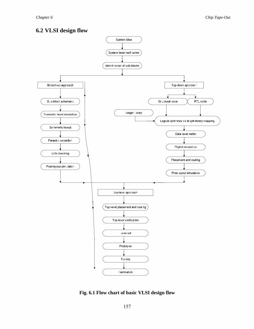
Chapter 6 Chip Tape-Out
157
6.2 VLSI design flow
Fig. 6.1 Flow chart of basic VLSI design flow
Chapter 6 Chip Tape-Out
158
6.2.1 Bottom-up (Back-end design) approach Sub-block schematic:
This section gives the schematic implementation of logic circuit at transistor level. The
passive and active devices can be taken from analog library of EDA tool and then will be
connected to construct logic circuit. Symbols can also be included as connecting devices
which can be created from circuit using EDA tool. After placing all the devices in
appropriate places, routing is done through wiring. All the input and output nodes are
connected to pins with appropriate direction. Every circuit must be biased with DC power
supply that varies according to process technology for minimum supply voltage below
which the circuit cannot operate. Thus proper bias voltage source needs to be connected
and grounding of whole circuit must be ensured.
Transistor level simulation:
The functionality of sub-block schematic circuit needs to be verified which is done at
transistor level simulation stage through waveforms of input and output pins. There are
two types of verification: functional and formal verification. As this work is carried out in
bottom-up approach, only functional verification is possible. Once output is following the
functionality of the designed logic circuit, then it can be processed to layout level.
Schematic layout:
This is built on stick diagram of circuit which must be done manually before proceeding
for layout. Once stick diagram is finished then standard layout is to be drawn for logic
circuit accordingly. Before taking it to layout environment, all the input and bias power
supply sources must be removed from schematic circuit and the resultant circuit will be left
with input and output pins. Ground and power supply pins need to be replaced by input-
output direction pins. The EDA tool will provide all the required layers for drawing layout
with distinct colors. Apart from many layers, there are basic layers which are mostly used
such as Metal1, Poly, N-Well and Diffusion (both p-type and n-type) layers. Also, for
connecting these layers, contacts are used. All these components, including various layers
and contacts, possess minimum size to be maintained while drawing in order to reduce the
overhead area failing which leads to DRC (Design Rule Check) errors. Thus once layout is
drawn then EDA tool will check for DRC errors. All the layers must satisfy, the design
Chapter 6 Chip Tape-Out
159
rules which include, minimum width of layers, spacing between layers, type of contacts
taken with appropriate size and color, labeling or naming the corresponding nodes and
others.
Parasitic extraction:
After DRC is finished without errors, the layout will be taken to next stage called parasitic
extraction for extracting parasitic components which include inbuilt resistors and
capacitors at various nodes inside the circuit. In spite of being very small in magnitude,
these will contribute notable impact on the performance of circuit through signal integrity
issues which are discussed in chapter 4. For example, the major inevitable problems like
charge sharing, leakage currents, capacitive coupling are few consequences due to parasitic
components.
LVS check:
Layout versus schematic checking is required for checking the dissimilarities between the
schematic of circuit and layout version. LVS should match so that post-layout simulation is
possible. LVS checking needs matching of all the nodes, connections, appropriate layers,
input-output pins and their corresponding names. When LVS checking is matched properly
then post level simulation is done.
Post-layout simulation:
The name itself indicates that the simulation usually done after the layout is drawn. The
significance of repeating simulation procedure again at this level is to investigate the
impact of circuit parasitic components on the performance of designed logic circuit
functionality. It is the verification of complete design with all constraints added after
creation of layout. Therefore, if any error is encountered at this stage, then circuit needs to
be amended to nullify the concerned error. Normally, owing to the presence of circuit
parasites, more power is consumed when compared to simulation at schematic level.
Moreover, propagation delay may also be increased. Thus, having finished this post-layout
simulation, the bottom-up approach along with top-down approach converges to top-level
approach and will be subjected to various top-level ambient conditions involved in final
Chapter 6 Chip Tape-Out
160
fabrication process of manufacturing the electronic circuit chip. The top-down approach is
briefed up in sub-section 6.2.2.
6.2.2 Top-down (Front-end design) approach Firstly, coding is done using hardware description languages such as VHDL or Verilog by
the designer out of which the gate level net-list will be generated. The coding can be of any
type. The structural and RTL code will be synthesized with the help of target library
standard files. The synthesis results in creation of gate level net-list which needs to
undergo digital simulation. This is functional verification. Test bench can also be written
for functional verification which is more effective than normal digital simulation. After
digital simulation, placement and routing that includes positioning the components on chip
and connecting all the I/O ports with pins using wiring, is done after which post-layout
simulation is processed. This implies that post-layout simulation is common procedure
before frond-end and back-end designs converge into top-level approach.
6.2.3 Top-level approach Top-level approach is the final stage in the VLSI flow that includes making of test chip for
circuit design. It starts with placement and routing to make sure that all the I/O pins and
devices are properly placed and connected. Then verification of design takes place and is
common phenomenon which, in fact, needs to be done at each and every level to make
design more accurate and faultless. Next comes, chip tape-out which generates a photo
mask of designed circuit that will be sent to final fabrication of chip. Chip tape-out results
in prototype chip which is a sample model for testing the designed circuit to even enhance
the accuracy and precision further. Once it gets tested and is found to be error-free then
manufacturing engineers will go for final fabrication of test-chip.
The complete VLSI flow is shown in Fig. 6.1 where this test-chip of proposed circuit is
done using back-end approach. All the related data is provided along with design
specifications which include dimensions of devices taken (width and length of channel),
supply voltage and applied input voltage.
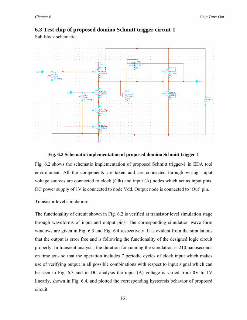
Chapter 6 Chip Tape-Out
161
6.3 Test chip of proposed domino Schmitt trigger circuit-1 Sub-block schematic:
Fig. 6.2 Schematic implementation of proposed domino Schmitt trigger-1
Fig. 6.2 shows the schematic implementation of proposed Schmitt trigger-1 in EDA tool
environment. All the components are taken and are connected through wiring. Input
voltage sources are connected to clock (Clk) and input (A) nodes which act as input pins.
DC power supply of 1V is connected to node Vdd. Output node is connected to ‘Out’ pin.
Transistor level simulation:
The functionality of circuit shown in Fig. 6.2 is verified at transistor level simulation stage
through waveforms of input and output pins. The corresponding simulation wave form
windows are given in Fig. 6.3 and Fig. 6.4 respectively. It is evident from the simulations
that the output is error free and is following the functionality of the designed logic circuit
properly. In transient analysis, the duration for running the simulation is 210 nanoseconds
on time axis so that the operation includes 7 periodic cycles of clock input which makes
use of verifying output in all possible combinations with respect to input signal which can
be seen in Fig. 6.3 and in DC analysis the input (A) voltage is varied from 0V to 1V
linearly, shown in Fig. 6.4, and plotted the corresponding hysteresis behavior of proposed
circuit.
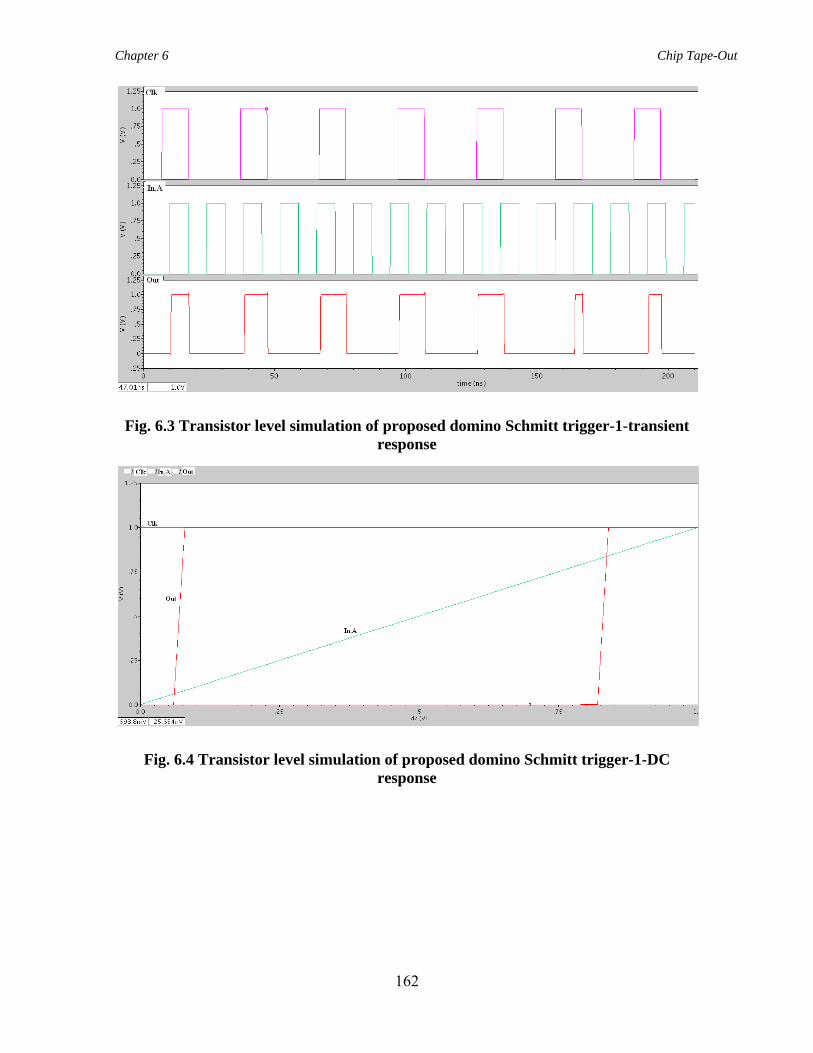
Chapter 6 Chip Tape-Out
162
Fig. 6.3 Transistor level simulation of proposed domino Schmitt trigger-1-transient response
Fig. 6.4 Transistor level simulation of proposed domino Schmitt trigger-1-DC response
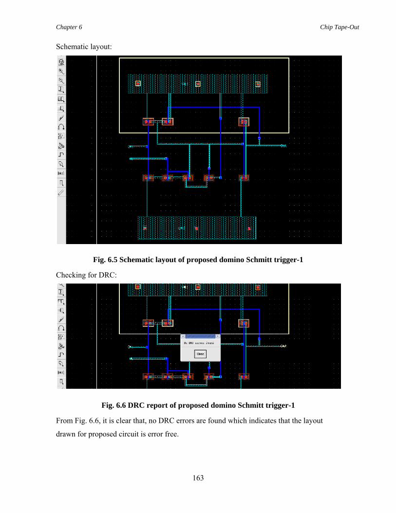
Chapter 6 Chip Tape-Out
163
Schematic layout:
Fig. 6.5 Schematic layout of proposed domino Schmitt trigger-1
Checking for DRC:
Fig. 6.6 DRC report of proposed domino Schmitt trigger-1
From Fig. 6.6, it is clear that, no DRC errors are found which indicates that the layout
drawn for proposed circuit is error free.
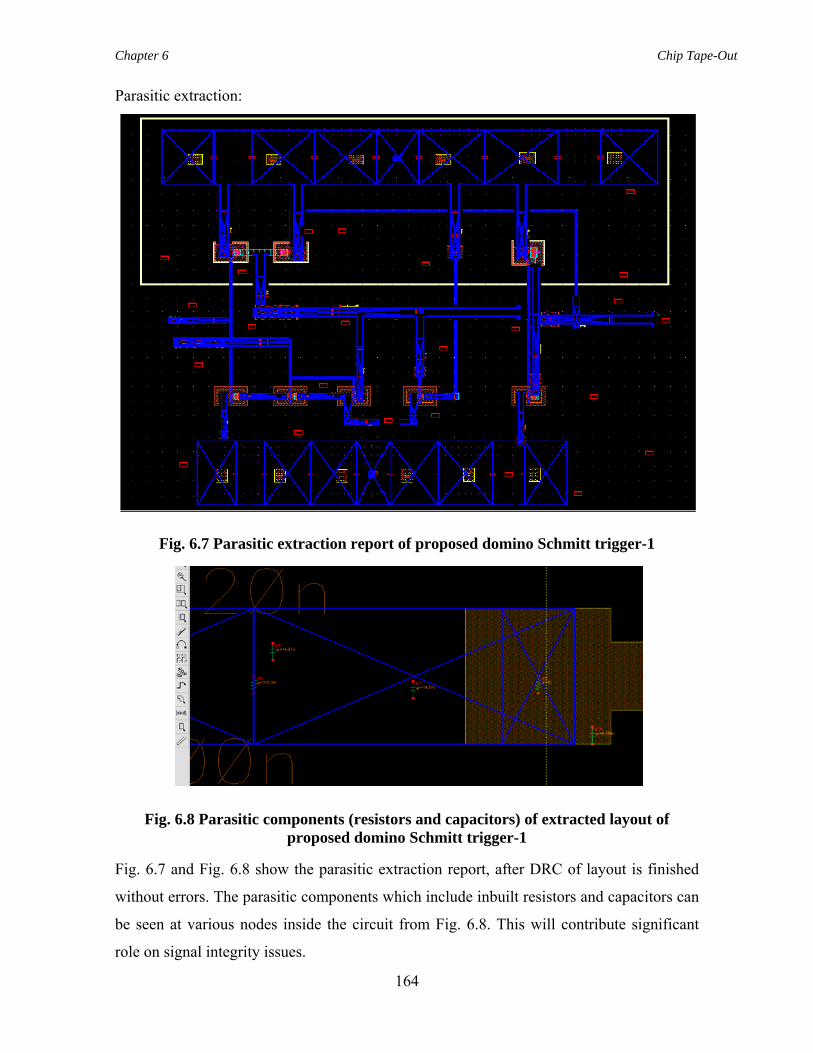
Chapter 6 Chip Tape-Out
164
Parasitic extraction:
Fig. 6.7 Parasitic extraction report of proposed domino Schmitt trigger-1
Fig. 6.8 Parasitic components (resistors and capacitors) of extracted layout of proposed domino Schmitt trigger-1
Fig. 6.7 and Fig. 6.8 show the parasitic extraction report, after DRC of layout is finished
without errors. The parasitic components which include inbuilt resistors and capacitors can
be seen at various nodes inside the circuit from Fig. 6.8. This will contribute significant
role on signal integrity issues.
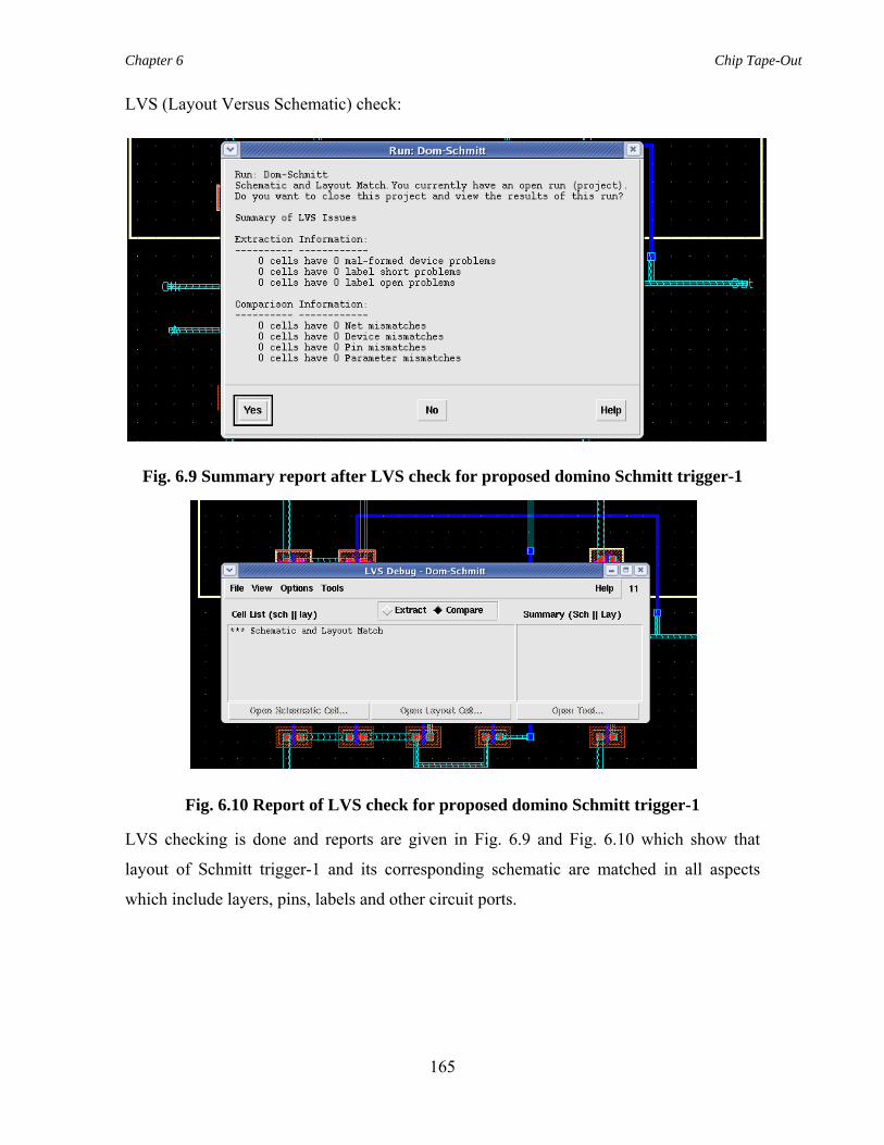
Chapter 6 Chip Tape-Out
165
LVS (Layout Versus Schematic) check:
Fig. 6.9 Summary report after LVS check for proposed domino Schmitt trigger-1
Fig. 6.10 Report of LVS check for proposed domino Schmitt trigger-1
LVS checking is done and reports are given in Fig. 6.9 and Fig. 6.10 which show that
layout of Schmitt trigger-1 and its corresponding schematic are matched in all aspects
which include layers, pins, labels and other circuit ports.
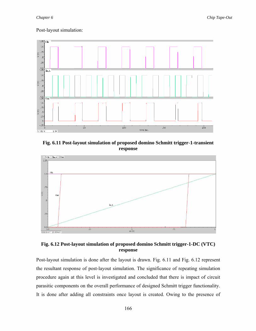
Chapter 6 Chip Tape-Out
166
Post-layout simulation:
Fig. 6.11 Post-layout simulation of proposed domino Schmitt trigger-1-transient response
Fig. 6.12 Post-layout simulation of proposed domino Schmitt trigger-1-DC (VTC) response
Post-layout simulation is done after the layout is drawn. Fig. 6.11 and Fig. 6.12 represent
the resultant response of post-layout simulation. The significance of repeating simulation
procedure again at this level is investigated and concluded that there is impact of circuit
parasitic components on the overall performance of designed Schmitt trigger functionality.
It is done after adding all constraints once layout is created. Owing to the presence of
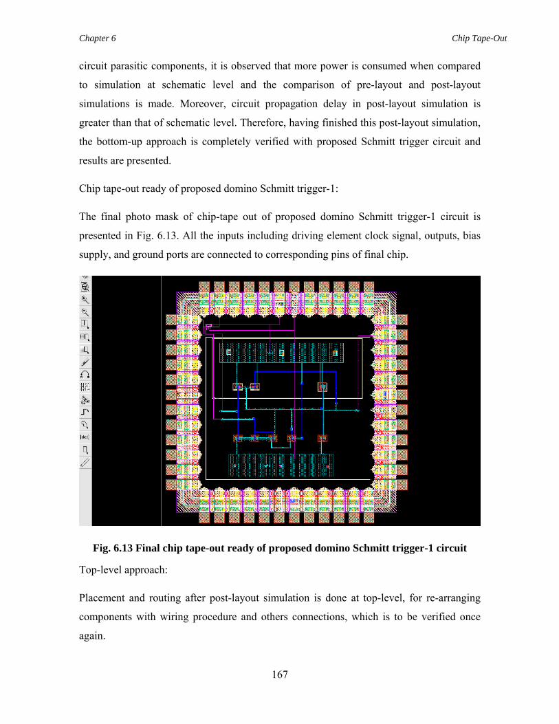
Chapter 6 Chip Tape-Out
167
circuit parasitic components, it is observed that more power is consumed when compared
to simulation at schematic level and the comparison of pre-layout and post-layout
simulations is made. Moreover, circuit propagation delay in post-layout simulation is
greater than that of schematic level. Therefore, having finished this post-layout simulation,
the bottom-up approach is completely verified with proposed Schmitt trigger circuit and
results are presented.
Chip tape-out ready of proposed domino Schmitt trigger-1:
The final photo mask of chip-tape out of proposed domino Schmitt trigger-1 circuit is
presented in Fig. 6.13. All the inputs including driving element clock signal, outputs, bias
supply, and ground ports are connected to corresponding pins of final chip.
Fig. 6.13 Final chip tape-out ready of proposed domino Schmitt trigger-1 circuit
Top-level approach:
Placement and routing after post-layout simulation is done at top-level, for re-arranging
components with wiring procedure and others connections, which is to be verified once
again.
Chapter 6 Chip Tape-Out
168
Chip tape-out:
Thus, final chip-tape out is made for proposed domino Schmitt trigger-1 and its photo
mask will next be sent to fabrication lab for manufacturing IC chip. Tape-out is pre-
fabrication stage where the photo mask of final result is given to the manufacturers. Then,
physical fabrication will be done which includes steps such as wafer marching, packing,
testing and finally followed by design of physical Integrated circuit chip.
Fabrication:
A fine response at post-layout simulation level does not always ensure a productive
outcome since the verification of real-time performance of the chip could only be done by
testing the fabricated prototype. The final step in IC design flow is adding pads to the
circuit. Once it is done successfully, the chip will then be sent to fabrication lab for
manufacturing. In spite of using the step called parasitic extraction for identifying the
realistic performance of circuit conditions extended to a higher order degree from the
actual photo mask layout level, most of the extraction procedures along with simulation
models, employed especially in latest advanced design tools, possess inevitable boundary
restrictions which must always be one of the main design considerations from very basic
level.
Final testing:
Having finished the manufacturing of chip, final testing has to be carried out once again
for checking its over functionality and if the response is matched with circuit desired
functionality then that IC will be released in market and will be brought to customer.
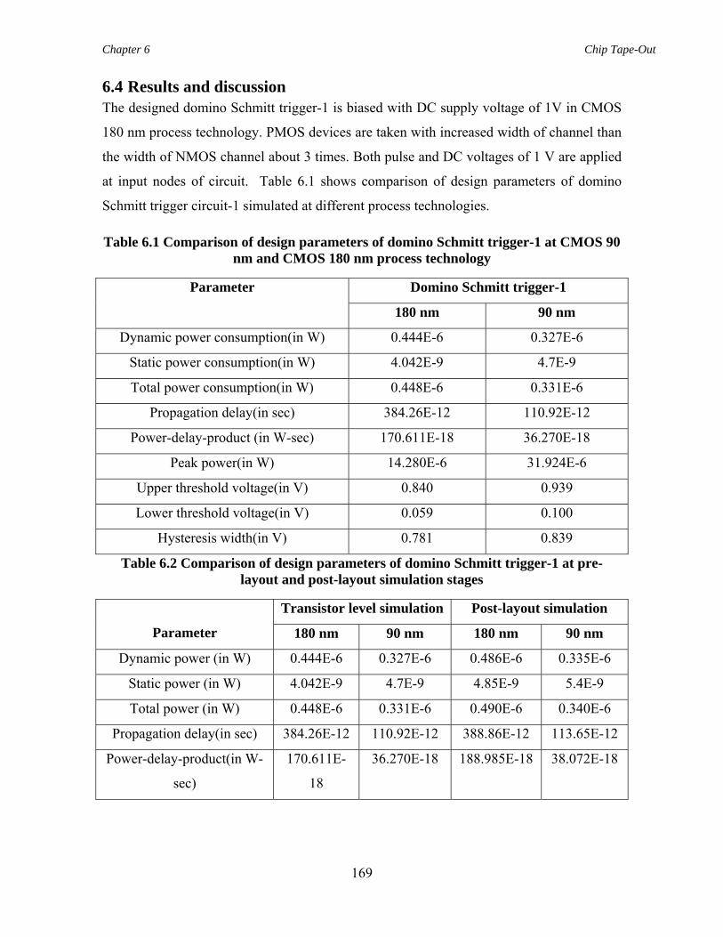
Chapter 6 Chip Tape-Out
169
6.4 Results and discussion The designed domino Schmitt trigger-1 is biased with DC supply voltage of 1V in CMOS
180 nm process technology. PMOS devices are taken with increased width of channel than
the width of NMOS channel about 3 times. Both pulse and DC voltages of 1 V are applied
at input nodes of circuit. Table 6.1 shows comparison of design parameters of domino
Schmitt trigger circuit-1 simulated at different process technologies.
Table 6.1 Comparison of design parameters of domino Schmitt trigger-1 at CMOS 90 nm and CMOS 180 nm process technology
Parameter Domino Schmitt trigger-1
180 nm 90 nm
Dynamic power consumption(in W) 0.444E-6 0.327E-6
Static power consumption(in W) 4.042E-9 4.7E-9
Total power consumption(in W) 0.448E-6 0.331E-6
Propagation delay(in sec) 384.26E-12 110.92E-12
Power-delay-product (in W-sec) 170.611E-18 36.270E-18
Peak power(in W) 14.280E-6 31.924E-6
Upper threshold voltage(in V) 0.840 0.939
Lower threshold voltage(in V) 0.059 0.100
Hysteresis width(in V) 0.781 0.839
Table 6.2 Comparison of design parameters of domino Schmitt trigger-1 at pre-layout and post-layout simulation stages
Parameter
Transistor level simulation Post-layout simulation
180 nm 90 nm 180 nm 90 nm
Dynamic power (in W) 0.444E-6 0.327E-6 0.486E-6 0.335E-6
Static power (in W) 4.042E-9 4.7E-9 4.85E-9 5.4E-9
Total power (in W) 0.448E-6 0.331E-6 0.490E-6 0.340E-6
Propagation delay(in sec) 384.26E-12 110.92E-12 388.86E-12 113.65E-12
Power-delay-product(in W-
sec)
170.611E-
18
36.270E-18 188.985E-18 38.072E-18

Chapter 6 Chip Tape-Out
170
Discussion
From Table 6.1, it is clear that, the propagation delay and power-delay-product in 90 nm
process technology are less than those of 180 nm process technology. This is due to
reduced transit time for carriers across the length of channel which results in increased
speed of operation of device. Besides transient analysis, peak power and hysteresis width
are observed to be increased in DC analysis in 90 nm process technology.
Table 6.2 compares the computed design parameters at transistor level (pre-layout) and
post-layout simulations. Compared to pre-layout simulation, post-layout simulation results
are observed to be increased in all design parameters. This is the resultant of inclusion of
extraction process of parasitic components from the layout of proposed circuit. Since, these
parasites provide conducting path in off state of device, static power dissipation increases.
Moreover, propagation delay and power-delay-product seem to be raised both in 90 nm
and 180 nm process technologies in post-layout simulation.
6.5 Conclusion The domino logic based Schmitt trigger-1 is designed and is simulated in CMOS 180 nm
process technology platform and observed significant variation in the simulation results
through comparison from the tabulations provided. The circuit analysis is carried out
through the dominant performance parameters like power consumption, propagation delay
and hysteresis width. Table 6.1 and Table 6.2 give the comparison of design parameters of
domino Schmitt trigger-1. The chip tape-out of proposed domino Schmitt trigger circuit-1
is done in CMOS 180 nm process technology. As a whole, in this chapter, the bottom-up
approach of the basic VLSI design flow is followed while designing chip tape out as this
work is carried out in analog environment that starts the designing of circuits from sub-
block schematic level and converges to top-level approach after post-level simulation
stage. The chip-tape out is being sent for fabrication.
Furthermore, this chip is not yet physically fabricated. We provide the prototype of
test-chip ready to vendor so that the final process could be carried out in fabrication lab. In
any case, this is not a part of the thesis. However, we will publish fabrication and test
results on a later date as a part IP of our lab.
Chapter 7 Conclusions & Future work
171
CHAPTER 7 CONCLUSIONS & FUTURE WORK
7.1 Conclusions The general conclusions drawn from this thesis and some suggested new directions
of research are presented in this chapter. The rapid evolution of VLSI technology
established a remarkable transformation in the fabrication industry with its emerging
qualities like high speed and low area overhead. Scaling brought impeccable change in the
recent trends. Power consumption, noise immunity, speed of operation, area and cost are
the predominant parameters that have to be taken into consideration before designing any
kind of digital logic circuit technique. There may be a trade-off between any two
parameters depending on the situation and application of design. Sometimes, the design
techniques might not meet all the mentioned requirements in their application, but still an
optimization may be followed in order to proceed further in research areas. Because of
high speed and low overhead area domino logic became process of choice for many digital
designs. However, the real alarming issues are large power consumption and high noise
sensitivity. Hence, there is a need for designing new domino methodology or improving
existing techniques to meet the requirements by overcoming the above drawbacks.
Therefore, the outcome of research must be able to handle the primary design parameters
effectively. Besides this, the designed circuit must exhibit high degree of noise robustness.
General conclusions
The work done in this thesis to achieve above mentioned objective is summarized
below.
Novel domino topologies
The research area-Domino logic is primarily focused on present working
environment from a broader angle with the study of standard logic styles and related work
in brief. This thesis proposed novel domino logic circuit techniques to deal with noise and
sub-threshold leakages. Furthermore, existing circuits are also modified to improve the
response. When compared to existing techniques, proposed logic techniques are very
effective in increasing the immunity of system towards noise and sub-threshold leakage
issues. Energy-efficient circuits are proposed in chapter 3 which explore conditional
Chapter 7 Conclusions & Future work
172
keepers very efficaciously to sustain from noise glitches and sub-threshold leakage
currents. Computations of noise metric parameters like UNG and ANTE are done for all
proposed circuit techniques to examine how robust they are for noise affects. From the
calculations of UNG, it is evident that the proposed domino circuit techniques are
exhibiting superior noise metric parameter-UNG which is almost nearer to unity factor (1)
that reveals its improved noise robustness. The proposed circuits score over existing
circuits in terms of noise and leakage reduction and this is established through
corresponding UNG and ANTE comparisons.
Process corner analysis
Moreover, all the existing and proposed circuits are subjected to distinct process
corners like NN, FF, SS, FS and SF, to investigate the change in the performance. Having
done the process corner analysis, it is observed that despite few limitations and boundary
conditions, proposed circuit techniques are exhibiting high degree of noise robustness with
reduced leakage power. Furthermore, the trade-off between power consumption and
propagation delay is effectively optimized. All the computational results are tabulated and
comparison is made followed by analysis through discussion. Results reveal that proposed
techniques are very strong enough against noise glitches.
Signal integrity issues
Besides these techniques, there is other proposed circuit technique for stabilizing
dynamic node which is presented in chapter 4 to avoid the leakage drop from dynamic
node. It also acts as low power technique with increased number of PMOS stack
transistors. Lector based domino technique also reduced leakage power and it increased
UNG and ANTE noise parameters.
Schmitt trigger using domino
Domino based Schmitt trigger circuits are also proposed with large hysteresis and
zero hysteresis voltages which find variety of applications. Particularly large hysteresis
domino Schmitt trigger circuit is effective in improving noisy immunity of the system
while the other Schmitt trigger with zero hysteresis finds applications in I/O pads. Both are
exhibiting superior performance in primary design parameters like dynamic power, leakage
power, propagation delay, hysteresis width and noise metric parameters which include
UNG and ANTE.
Chapter 7 Conclusions & Future work
173
Test chip tape-out ready
A test chip of Domino Schmitt Trigger is also fabricated using UMC 180 nm
technology.
The complete analysis of versatile domino logic circuits is carried out at different process
ambient conditions. Existing Domino logic circuits are investigated thoroughly and issues
related to this logic style are brought out. The significant variations in design parameters
are also noted in all circuit techniques through simulation while improving the
performance in various aspects. There are a few pros and cons with proposed techniques in
certain parameters. In certain cases while improving a particular design parameter, there is
notable deterioration in quality of other parameters which may be worsening the situation,
causing drawbacks. However, we have come up with circuits that facilitate leakage
reduction, increase the speed of operation, improved noise robustness and low power
consumption further. Furthermore, novel Schmitt trigger circuits are designed indicates
superior performance in terms of power consumption, propagation delay and hysteresis
width.
7.2 Future work There are ample opportunities to explore advanced research based on this work. This work
can further be extended to improve the performance in all design parameters. Complete
elimination of signal integrity issues like charge leakage, charge sharing and capacitive
coupling effects is not possible as they are inevitable in all circuits. However, mitigating
them in a comparative manner with existing schemes facilitates to proceed further to
explore improved quality of research. Proposed circuit techniques too have few limitations
at some process corners which can be investigated thoroughly and can be improved further
striving for the best outcome.
174
Bibliography [1] J. M. Rabaey, A. Chandrakasan and B. Nikolic, Eds., Scholtz, "Digital Integrated
Circuits: A Design Perspective,” 2ed. low price edition 2005.
[2] N. Weste and K. Eshraghian, “Principles of CMOS VLSI Design-A Systems
Perspective,” Addison-Wesley, 2nd ed., 2003.
[3] H. Kaeslin, “Digital integrated Circuit Design-From VLSI Architecture to CMOS
Fabrication,” Cambridge University Press, 2008.
[4] J. Uyemura, “Physical Design of CMOS Integrated Circuits Using L-Edit,” PWS
publishing Company, 1995.
[5] W. Bhanzhaf, “Computer Aided Analysis Using PSPICE,” 2nd ed., Prentice Hall,
1992.
[6] Pierret, “Semiconductor Device Fundamentals,” Addison-Wesley, 2nd ed., 1996.
[7] B. Streetman, “Solid State Electronic Devices,” Prentice Hall, 2nd ed., 1995.
[8] A. Sedra and K. Smith, “MicroElectronic Cirucuits,” 4th ed., New York Oxford,
1998.
[9] H. Kaeslin, “Digital integrated Circuit Design-From VLSI Architecture to CMOS
Fabrication,” Cambridge University Press, 2008.
[10] H. L. Yeager, S.E. Siers, and B.T. Ormson, “Domino Circuit Topology,” U. S.
Patent 6784695, Aug. 31, 2004.
[11] S. M. Sharroush, Y. S. Abdalla, A. A. Dessouki, E. A. El-badawy, “Impact of
technology scaling on the performance of domino CMOS logic,” IEEE.Conference
proceed., 2003.
[12] N. Min-Allah, Y. Wang, J.Xing, W, Nisar, and A.Kazmi, “Towards Dynamic
Voltage Scaling in Real-Time Systems-A Survey,” International Journal of
Computer Sciences and Engineering Systems, vol. 1, no. 2, April 2007.
[13] M. W. Allam, “New Methodologies for Low-Power High-Performance Digital
VLSI Design,” Doctor of Philosophy Thesis, Waterloo, Ontario, Canada, 1999.
[14] S. Mukhopadhyay et al, “Gate Leakage Reduction for Scaled Devices using
Transistor Stacking,” IEEE Trans. On Very Large Scale Integration (VLSI)
Systems, vol. 11, no. 4, August, 2003.
[15] R. Hussain, “High performance ASIC Design: Using Synthesizable Domino logic
in an ASIC Flow,” Cambridge University Press, 2008.
175
[16] G. P. D’Souza, “Dynamic logic circuit with reduced charge leakage,” U.S. Patent
5483181, Jan. 9, 1996.
[17] G. Balamurugan, N. R. Shanbhag, “The Twin-transistor Noise Tolerant Dynamic
Circuit Technique,” IEEE JSSC, vol. 36, no. 2, Feb. 2001.
[18] M. E. S. Elrabaa, M. H. Anis, M. I. Elmasry, “A contention-free domino logic for
scaled-down CMOS technologies with ultra low threshold voltages,” ISCAS, May
2000.
[19] M. H. Anis, M. W. Allam, M. E. S. Elrabaa, “Energy efficient noise-tolerant
dynamic styles for scaled-down CMOS and MTCMOS technologies,” IEEE Trans.
VLSI Systs., vol. 10, no. 2, April 2002.
[20] G. Yee, C. Sechen, “Clock-Delayed Domino for Dynamic Circuit Design,” IEEE
Transaction on VLSI, vol. 8, no. 4, Aug. 2000.
[21] R. K. Krishnamurthy, A. Alvandpour, G. Balamurugan, N. R. Shanbhag, K.
Soumyanath, S. Y. Borkar, “A 130-nm 6-GHz 256 x 32 bit leakage-tolerant register
file,” IEEE Journal of Solid-State Circuits, vol. 37, no. 5, pp. 624-632, May 2002.
[22] P. Gronowski, A. Chandrakasan, W. J. Bowhill “Issues in dynamic logic design,”
in Design of High-performance Microprocessor Circuits, , F. Fox Eds. Piscataway,
NJ:IEEE press, , ch. 8, pp. 140-157, 2001.
[23] A. Alvandpour, R. K. Krishnamurthy, K. Soumyanath, S. Y. Borkar, “A sub-130-
nm conditional keeper technique,” IEEE Journal of Solid-State Circuits, vol. 37,
no. 5, pp. 633-638, May 2002.
[24] S. O. Jung, S. M. Yoo, K. W. Kim, S. M. Kang, “Skew-Tolerant High-Speed
(STHS) domino logic,” in Proc. Of International Symposium 2001 on Circuits and
Systems, vol. 4, pp. 154-157, May 2001.
[25] F. Moradi, T. V. Cao, E. I. Vatajelu, A. Peiravi, H. Mahmoodi, D. T. Wisland,
“Domino logic designs for high-performance and leakage-tolerant applications,”
VLSI Journal of Integration, Elsevier, vol. 46, pp. 247-254, May 2012.
[26] K. Roy, S. Mukhopadhyay, H. Mahmoodi, “Leakage tolerant mechanisms and
leakage reduction techniques in deep-submicron CMOS circuits,” Proc. Of IEEE
vol. 91, pp. 305-327, 2003.
[27] S. H. Choi, K. Roy, “Domino noise model: a new crosstalk noise model for
dynamic logic circuits,” IEEE International Conference Soc, pp. 2.7-210, 2003.
176
[28] H. Mostafa, M. Anis, M. Elmasry, “Novel Timing Yield improvement Circuits for
High-Performance Low-Power Wide Fan-in Dynamic OR Gates, IEEE
Transactions on VLSI Systems, vol. 58, issue. 8, pp. 1785-1797, 2011.
[29] K.L Shepard., V Narayanan.: “Noise in deep submicron digital design”. Int. Conf.
Computer-Aided Design, ICCAD 96, Digest of Technical Papers, San Jose, CA,
USA, pp. 524–531, November 1996.
[30] F. Frustaci, P. Corsonello, S. Perri, “High-performance noise-tolerant circuit
techni- ques for CMOS dynamic logic,” IET Circuits Devices and Systems, pp.
537–548, 2008.
[31] D. V. Borkar,“Technology and design challenges for low power and high
Performance”. Proc. Int. Symp. Low Power Electronics and Design, ISLPED 99,
pp. 163–138, San Diego, CA, USA, August 1999.
[32] R.K Mahmoodi-Meimand H., K Roy. “Diode-footed domino: a leakage-tolerant
High fan-in dynamic circuit design style”, IEEE Trans. Very Large Scale Integr.
Syst.,51, (3), pp. 495–503, 2004.
[33] L. Wang., N .R Shanbhag “An energy-efficient noisetolerant dynamic circuit
Technique”, IEEE Trans. Circuits Syst. II, 47, (11), pp. 1300–1306, 2000.
[34] F. M. Hernandez, M. L. Aranda, V. Champac, “Noise-tolerance improvement in
dynamic CMOS logic circuits”, IEE Proc. Circuits, Devices Syst., 153, (6), pp.
565–573, 2006.
[35] P. Gronowski, A. Chandrakasan , W. J. Bowhill, W.J., Fox “Issues in dynamic
logic design’, in (EDS.): “Design of highperformance microprocessor circuits”
(IEEE Press, Piscataway,), Ch. 8, pp. 140–157, NJ , 2001.
[36] M.H Anis, M. W. Allam, M.W. Elmasry, “High-speed dynamic logic styles for
Scaled-down CMOS and MTCMOS technologies”. Proc. Int. Symp. Low Power
Electronics and Design, ISLPED 00, Rapallo, Italy, pp. 155–160, July 2000.
[37] M.H Anis., M.W Allam., M.I Elmasry. “Energy-efficient noisetolerant dynamic
styles for scaled-down CMOS and MTCMOS technologies”, IEEE Trans. Very
Large Scale Integr. Syst., 10, (2), pp. 71–78, 2002.
[38] J. J. Covino, “Dynamic CMOS circuits with noise immunity,” U.S. Patent
56507333, July 22, 1997.
177
[39] A Alvandpour., R.K Krishnamurthy., K. Soumyanath, S.Y Borkar.: “A Sub-130-
nm conditional keeper technique”, IEEE J. Solid-State Circuits, 37, (5), pp. 633–
638, 2002.
[40] H. Mahmoodi-Meimand, K.Roy, “Diode-footed domino: a leakage-tolerant high
fan-in dynamic circuit design style,” IEEE Transaction on Circuit and Systems I,
vol. 51, no. 3, pp. 495-503, Mar. 2004.
[41] S. Jung, S. Yoo, K Kim., S. Kang: “Skew-tolerant highspeed (STHS) domino
Logic”. IEEE Int. Symp. Circuits and Systems, ISCAS 01, Sydney, Australia, vol.
4, pp. 154–157, May 2001.
[42] J. Kim., K. Roy, “ A leakage tolerant high fan-in dynamic circuit design
technique”.Proc. 27th European Solid-State Circ. Conf., ESSCIRC, Villach,
Austria, pp. 309–312, September 2001.
[43] F Frustaci., P Corsonello., G Cocorullo.: “A new noise-tolerant dynamic logic
circuit design’, IEEE Ph.D. Research in Microelectronics and Electronics, PRIME
2007, Bordeaux, France, pp. 61–64, July 2007.
[44] B.Y Cao., M. Orshansky, T. Sato, D. Sylvester,”Spice up your MOSFET
modeling”, IEEE Circuits Devices Mag 19, (4), pp. 17–23, 2003.
[45] K. Roy, S. Mukhopadhyay, H. M. Meimand, “Leakage current mechanisms and
leakage reduction techniques in deep-submicron CMOS circuits”, Proc. IEEE, 91,
(2), pp. 305–327, 2003.
[46] M. Elgebaly., M. Sachdev: “A leakage tolerant energy efficient wide domino
circuit technique”. Proc. 45th Midwest Symp. Circuits Syst., MWSCAS 02, vol. 1,
pp. 487–490, Tulsa,Oklahoma, USA, August 2002.
[47] F Moradi., A. Peiravi, H. Mahmoodi: “A new leakagetolerant design for high fan-
in domino circuits”. Proc. 16th Int. Conf. Microelectr., ICM 04, pp. 493–496, Sfax,
Tunisia,December 2004.
[48] L. Wang, R.K.Krishnamurthy, K. Soumyanath, N.R Shanbhag.: ‘An energy-
efficient leakage-tolerant dynamic circuit technique’. Proc. 13th IEEE Int.
ASIC/SOC Conf.,pp. 221–225, Arlington, VA, USA, September 2000.
[49] M. Alito, G. Palumbo, M. Pennisi, “Understanding the Effect of process
Variations on the Delay of Static and Domino logic,” IEEE Transactions on VLSI
Systems, vol. 18, issue. 5, pp. 697-710, 2010.
178
[50] S. Weaver, B. Hersberg, N. Maghari, U-K Moon,“Domino-logic-based ADC for
digital synthesis,” IEEE Transactions on Circuits and Systems II: Express Briefs,
vol. 58, issue. 11, pp. 744-747, 2011.
[51] C. H. Kim, K. Roy, S. HSU, R. Krishnamurthy, S. Borkar, “ A process variation
compensating technique with on-die leakage current sensor for nanometre scale
dynamic circuits”IEEE Transactions on Circuits and SystemsI, vol. 53, pp.1704–
1711, Aug. 2006.
[52] M. Anis, S. Areibi, M. Elmasry, “Design and optimization of multi-threshold
CMOS (MTCMOS) circuits,” IEEE Transactions on Computer-Aided Design of
Integrated Circuits and Systems 22 (10) ,pp.1324–1342, 2003.
[53] M.W. Allam, M.H. Anis, M.I. Elmasry, “High speed dynamic logic style for
scaled- down CMOS and MTCMOS technologies,” in: Proceedings of the
International Symposium on Low Power Electronics and Design, pp. 175–180,
2000.
[54] F. Moradi, H. Mahmoodi, A. Peiravi, “A high speed and leakage-tolerant domino
logic for high fan-in gates,” in: Proceeding of the 15th ACM Great Lakes
Symposium on VLSI, (GLSVLSI), pp. 478–481, Chicago, IL, USA, 2005.
[55] O. Gonzalez-Diaz, M. Linares-Aranda, F. Mendoza-Herna´ndez, “A comparison
between noise-immunity design techniques for dynamic logic gates,” Midwest
Symposium on Circuits and Systems 1 pp. 484–488, 2006.
[56] H.F. Dadgour, K. Banerjee, “A novel variation-tolerant keeper architecture for
high- performance low-power wide fan-in dynamic or gates,” IEEE Transactions
on Very Large Scale Integration (VLSI) Systems 99,pp 1–12, 2010.
[57] K. Bernstein, D.J. Frank, A.E. Gattiker, W. Haensch, B.L. Ji, S.R. Nassif, E.J.
Nowak, D.J. Pearson, N.J. Rohrer, High-performance CMOS variability in the 65-
nm regime and beyond, IBM Journal of Research and Development 50 (4/5) pp.
433–449, 2006.
[58] H. J. M Veendrick, “Short circuit dissipation of static CMOS circuitry and its
impact on the design of buffer circuits,” IEEE J. Solid-State Circuits, vol. SC-19,
pp. 468–473, Aug. 1984.
[59] A. P. Chandrakasan and R. W. Brodersen, “Minimizing power consumption in
digital CMOS circuits,” Proc. IEEE, vol. 83, pp. 498-523, 1995.
179
[60] N. Hanchate, N. Ranganathan, “Lector: A Technique for leakage reduction in
CMOS Circuits,” IEEE Transactions on VLSI, vol 12, no. 2, Feb. 2004.
[61] R. X. Gu and M. I. Elmasry, “Power dissipation analysis and optimization for deep
submicron CMOS digital circuits,” IEEE J. Solid-State Circuits, vol. 31, pp 707-
713, May 1999.
[62] Q.Wang and S. Vrudhula, “Static power optimization of deep sub-micron CMOS
circuits for dual Vth technology,” in Proc. IC CAD, pp 490-496, April 1998.
[63] B. J. Sheu, D. L. Scharfetter, P. K. Ko, and M. C. Jeng, “BSIM: Berkeley short-
channel IGFET model for MOS transistors,” IEEE J. Solid- State Circuits, vol. SC-
22, pp. 558–566, Aug. 1987.
[64] S. Thompson, P. Packan, and M. Bohr, “MOS scaling: Transistor challenges for
the21st century,” Intel Technol. J., vol. Q3, 1998.
[65] J. P. Halter and F. Najm, “A gate-level leakage power reduction method for
ultralow- power CMOS circuits,” in Proc. IEEE Custom Integrated Circuits Conf.,
pp. 475–478 1997.
[66] D. Duarte, Y.-F. Tsai, N. Vijay Krishnan, and M. J. Irwin, “Evaluating run-time
techniques for leakage power reduction,” in 7th Proc. ASP-DAC, pp. 31–38, 2002.
[67] M. D. Powell, S.-H. Yang, B. Falsafi, K. Roy, and T. N. Vijaykumar, “Gated-Vdd:
A circuit technique to reduce leakage in deep submicron cache memories,” in Proc.
IEEE ISLPED, pp. 90–95, 2000.
[68] M. C. Johnson, D. Somasekhar, L. Y. Chiou, and K. Roy, “Leakage control with
efficient use of transistor stacks in single threshold CMOS,” IEEE Trans. VLSI
Syst., vol. 10, pp. 1–5, Feb. 2002.
[69] J. Kao, A. Chandrakasan, and D. Antoniadis, “Transistor sizing issues and tool for
multi-threshold CMOS technology,” in Proc. 34th DAC, pp. 409–414, 1997.
[70] C. Gopalakrishnan and S. Katkoori, “Resource allocation and binding approach
for low leakage power,” in Proc. IEEE Int. Conf. VLSI Design, pp. 297–302, Jan.
2003.
[71] L. Wei, Z. Chen, M. Johnson, and K. Roy, “Design and optimization of low
voltage high performance dual threshold CMOS circuits,” in Proc. 35th DAC, pp.
489–492, 1998.
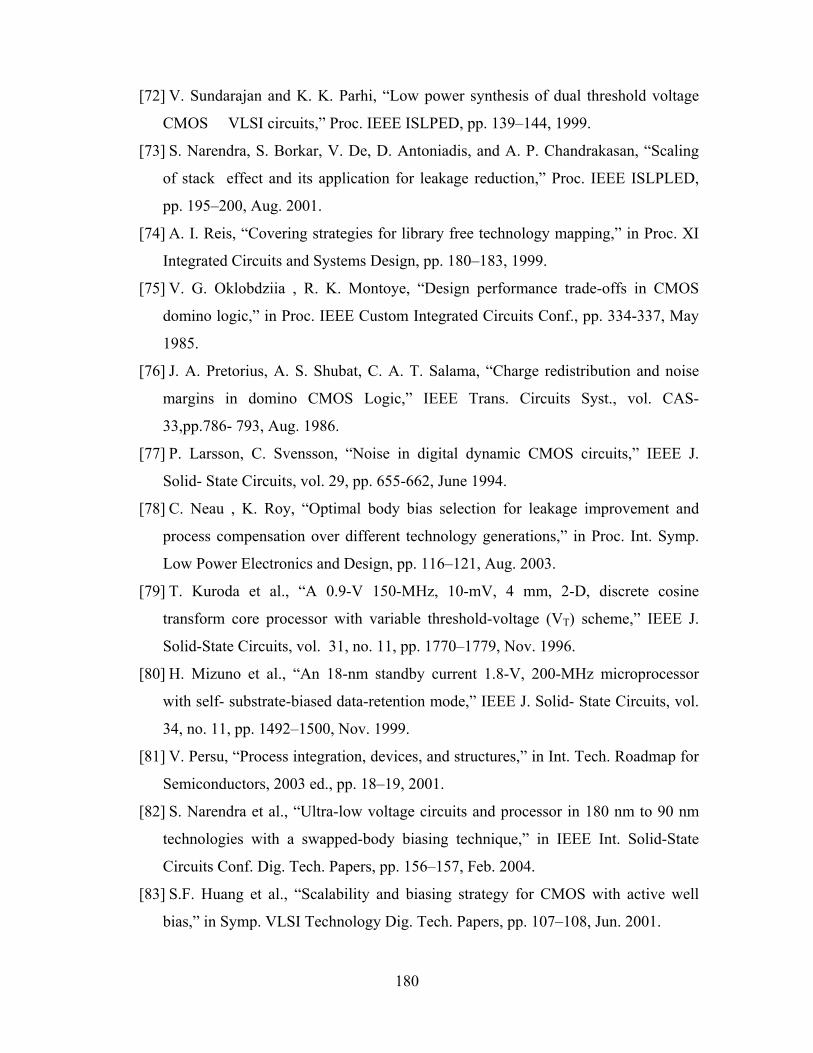
180
[72] V. Sundarajan and K. K. Parhi, “Low power synthesis of dual threshold voltage
CMOS VLSI circuits,” Proc. IEEE ISLPED, pp. 139–144, 1999.
[73] S. Narendra, S. Borkar, V. De, D. Antoniadis, and A. P. Chandrakasan, “Scaling
of stack effect and its application for leakage reduction,” Proc. IEEE ISLPLED,
pp. 195–200, Aug. 2001.
[74] A. I. Reis, “Covering strategies for library free technology mapping,” in Proc. XI
Integrated Circuits and Systems Design, pp. 180–183, 1999.
[75] V. G. Oklobdziia , R. K. Montoye, “Design performance trade-offs in CMOS
domino logic,” in Proc. IEEE Custom Integrated Circuits Conf., pp. 334-337, May
1985.
[76] J. A. Pretorius, A. S. Shubat, C. A. T. Salama, “Charge redistribution and noise
margins in domino CMOS Logic,” IEEE Trans. Circuits Syst., vol. CAS-
33,pp.786- 793, Aug. 1986.
[77] P. Larsson, C. Svensson, “Noise in digital dynamic CMOS circuits,” IEEE J.
Solid- State Circuits, vol. 29, pp. 655-662, June 1994.
[78] C. Neau , K. Roy, “Optimal body bias selection for leakage improvement and
process compensation over different technology generations,” in Proc. Int. Symp.
Low Power Electronics and Design, pp. 116–121, Aug. 2003.
[79] T. Kuroda et al., “A 0.9-V 150-MHz, 10-mV, 4 mm, 2-D, discrete cosine
transform core processor with variable threshold-voltage (VT) scheme,” IEEE J.
Solid-State Circuits, vol. 31, no. 11, pp. 1770–1779, Nov. 1996.
[80] H. Mizuno et al., “An 18-nm standby current 1.8-V, 200-MHz microprocessor
with self- substrate-biased data-retention mode,” IEEE J. Solid- State Circuits, vol.
34, no. 11, pp. 1492–1500, Nov. 1999.
[81] V. Persu, “Process integration, devices, and structures,” in Int. Tech. Roadmap for
Semiconductors, 2003 ed., pp. 18–19, 2001.
[82] S. Narendra et al., “Ultra-low voltage circuits and processor in 180 nm to 90 nm
technologies with a swapped-body biasing technique,” in IEEE Int. Solid-State
Circuits Conf. Dig. Tech. Papers, pp. 156–157, Feb. 2004.
[83] S.F. Huang et al., “Scalability and biasing strategy for CMOS with active well
bias,” in Symp. VLSI Technology Dig. Tech. Papers, pp. 107–108, Jun. 2001.
181
[84] K. V Arnim, P. Seegebrecht, R. Thewes, and C. Pacha, “A low-leakage 2.5 GHz
skewed CMOS 32 b adder for nanometer CMOS technologies,” in IEEE Int. Solid-
State Circuit Conf. Dig. Tech. Papers, Feb. 2005.
[85] K. Kanda, K. Nose, H. Kawaguchi, and T. Sakurai, “Design impact of positive
temperature dependence on drain current in sub-1 V CMOS VLSI’s,” IEEE J.
Solid- State Circuits, vol. 36, no. 10, pp. 1559–1564, Oct. 2001.
[86] I. M. Filanovsky and A. Allam, “Mutual compensation of mobility and threshold
voltage temperature effects with applications in CMOS circuits,” IEEE Trans.
Circuits Syst. I, Analog Digit. Signal Process, vol. 48, no. 7, pp. 876–884, Jul.
2001.
[87] Y. Tsividis, “Operation and Modeling of the MOS Transistor,” 2nd ed. New York:
WCB/McGraw-Hill, 1999.
[88] K. Agawa, H. Hara, T. Takayanagi, T. Kuroda, “A bitline leakage compensation
scheme for low-voltage SRAMs,” IEEE J. Solid-State Circuits, vol. 36, pp. 726–
734, May 2001.
[89] H. Tanaka et al., “A precise on-chip voltage generator for a gigascale DRAM with
a negative wordline scheme,” IEEE J. Solid-State Circuits, vol. 34, pp. 1084–1090,
Aug. 1999.
[90] H. Kawaguchi, Y. Itaka, and T. Sakurai, “Dynamic leakage cut-off scheme for
low- voltage SRAMs,” in Symp. VLSI Circuits Dig. Tech. Papers, pp. 140–141,
June 1998.
[91] T. Kuroda et al., “A 0.9 V 150 MHz 10 mW 4 mm 2-D discrete cosine transform
core processor with variable threshold voltage scheme,” IEEE J. Solid-State
Circuits, vol. 31, pp. 1770–1779, November 1996.
[92] M. Golden and H. Partovi, “A 500-MHz write-bypassed 88-entry 90-bit register
file,” in Symp. VLSI Circuits Dig. Tech. Papers, pp. 105–108, June 1999.
[93] S. Tyagi et al., “A 130-nm generation logic technology featuring 70-nm
transistors, dual-Vt transistors and 6 layers of Cu interconnects,” in IEDM Tech.
Dig., pp.567–570, 2000.
[94] A. Alvandpour, R. Krishnamurthy, K. Soumyanath, and S. Borkar, “A conditional
keeper technique for sub-130-nm wide dynamic gates,” in Symp. VLSI Circuits
Dig. Tech. Papers, pp. 29–30, June 2001.
182
[95] M. Anders, R. Krishnamurthy, K. Soumyanath, R. Spotten, “Robustness of sub-
70-nm dynamic circuits: Analytical techniques and scaling trends,” in Symp. VLSI
Circuits Dig. Tech. Papers, pp. 23–24, June 2001.
[96] V.De and S. Borkar, “Technology and design challenges for low power and high
performance,” in International Symposium on Low Power Electronics and Design,
pp.163-168, 1999.
[97] K. Roy. et.al. “Leakage Current Mechanisms and Leakage Reduction Techniques
in Deep-Submicron CMOS circuits”, Proceedings of IEEE, Feb, 2003.
[98] N. Ye, Y. Borkar, S., and De, V., “A New Technique for Standby Leakage
reduction in High-Performance Circuits,” IEEE Symposium on VLSI Circuits, pp.
40-41, 1998.
[99] W. T. Shiue, “Leakage power Estimation and Minimization in VLSI circuits,”
IEEE International Conference in Circuits and Systems, 2001.
[100] J. T. Kao, A. P. Chandrakasan, “Dual-Threshold Voltage Techniques for Low-
Power
[101] Digital Circuits,” IEEE Journal of Solid State Circuits, 35(7), pp. 1009-1018,
July 2000.
[102] Y-F. Tsai, D.Duarte, N.Vijayakrishnan, M.J.irwin, “Implications of Technology
Scaling on Leakage Reduction Techniques”, IEEE/ACM Design Automation
Conference, Anaheim, CA, June 2003.
[103] Chris H. Kim, Kaushik Roy, “Dynamic VTH Scaling Scheme for Active Leakage
Powe Reduction”, IEEE Design Automation and Test, 2002.
[104] Z. Chen, L. Wei, M. Johnson, K. Roy, “Estimation of Standby Leakage Power in
CMOS Circuits Considering Accurate Modeling of Transistor Stacks”, IEEE
International Symposium on Low Power Electronics and Design, pp. 239-244,
1998.
[105] J. Sheu, D.L. Scharfetter, P.K. Ko and M.C.Jeng, “BSIM: Berkely short channel
IGFET Model for MOS transistor”, IEEE J. Solid State Circuits, SC-22, 1987.
[106] C. Chen, A. Srivastava, M. Sarrafzadeh. “On gate level power optimization
using dual-supply voltages,” IEEE Trans. VLSI Systems, vol. 9 no 65, Oct. 2001.

183
[107] S. J. Shieh and J. S. Wang. “Design of low-power domino circuits using multiple
supply voltages,” In Proc. IEEE Int. Conf. Electronics, Circuits and Systems, pp.
711- 14, 2001.
[108] T. Sakurai and A. R. Newton. “Alpha-power law mosfet model and its
application to CMOS inverter delay and other formulas,” IEEE J. Solid State
Circuits, vol 29, pp. 655-662, June 1994.
[109] A. Rjoub, O. Koufopavlou, and S. Nikolaidis, “Low power / low swing domino
CMOS logic,” In Proc. IEEE Int. Symp. Circuits and Systems, pages II.13-II.16,
1998.
[110] I. M. Filanovsky and A. Allam, “Mutual compensation of mobility and threshold
voltage temperature effects with applications in CMOS circuits,” IEEE Trans.
Circuits Syst. I, Analog Digit. Signal Process, vol. 48, no. 7, pp. 876–884, Jul.
2001.
[111] V.De and S. Borkar, “Technology and design challenges for low power and high
performance,” in International Symposium on Low Power Electronics and Design,
pp.163-168, 1999.
[112] Y. Tsividis, Operation and Modeling of the MOS Transistor, 2nd ed. New York:
WCB/McGraw-Hill, 1999.
[113] K. Kanda, K. Nose, H. Kawaguchi, and T. Sakurai, “Design impact of positive-
temperature dependence on drain current in sub-1 V CMOS VLSI’s,” IEEE J.
Solid- State Circuits, vol. 36, no. 10, pp. 1559–1564, Oct. 2001.
[114] Z. Chen, M. Johnson, L. Wei, and K. Roy, “Estimation of standby leakage
power in CMOS circuits considering accurate modeling of transistor stacks,” In
Proc. Int. Symp. Low Power Electronics and Design, pp . 239-244, 1998.
[115] M. Igarashi, K. Usami, K. Nogami, F. Minami, Y. Kawasaki, T. Aoki, M.
Takano, C. Mizuno, T. Ishikawa, M. Kanazawa, and S. S, “A Low-power design
method using multiple supply voltages” In Proc. Int. Symp. Low Power Electronics
and Design, pp. 36-41, 1997.
[116] A. Peiravi, M. Asyaei, “Current-comparison-based domino:new low leakage
high speed domino circuit for wide fan-in gates”, IEEE trans. on VLSI systems,
vol. 21, no. 5, pp. 934-943, 2013.
184
[117] G. Palumbo, M. Pennissi, M. Alioto, “A simple circuit approach to reduce delay
variations in domino logic gates”, IEEE trans on circuits and systems I, vol. 59, no.
10, pp. 2292-2300, 2012.
[118] K. Yelamarthi, C.I.H. Chen, “Timing optimization and noise tolerance for
dynamic cmos susceptible to process variations”, IEEE trans on semiconductor
manufacturing, vol. 25, no. 2, pp. 255-265, 2012.
[119] N. Gong, J. Wang, R. Sridhar, “Variation aware sleep vector selection in dual Vt
dynamic OR circuits for low leakage register file design”, IEEE trans on circuits
and systems I, vol. 61, no. 7, pp. 1970-1983, 2014.
[120] H.F. Dadgour, K. Banerjee, “A novel variation-tolerant keeper architecture for
high performance low power wide fan-in dynamic OR gates”, IEEE trans on VLSI
systems, vol. 18, no. 11, pp. 1567-1577. 2010.
[121] H.Mostafa, M.Anis, M.Elmasry, “Novel timing yield improvement circuits for
high performance low power wide fan-in dynamic OR gates”, IEEE trans on
circuits and systems I, vol. 58, no. 8, pp. 1785-1797, 2011.
[122] M. Alioto, G. Palumbo, M. Pennissi, “A simple keeper topology to reduce delay
variations in nanometer domino logic”, IEEE International symposium circuits and
systems (ISCAS), pp. 1576-1579, 2012.
List of Publications
Conferences
[1] D.S.V.S.Sarma,K.K.Mahapatra,”Improved techniques for high performance noise-
tolerant domino CMOS logic circuits, “Students Conference on Engineering and Systems
(SCES)-2012, pp. 1-6, 2012.