Embed Size (px)
Citation preview

i
DESIGN AND IMPLEMENTATION OF A VOLTAGE SOURCE CONVERTER BASED HYBRID ACTIVE POWER FILTER
A THESIS SUBMITTED TO THE GRADUATE SCHOOL OF NATURAL AND APPLIED SCIENCES
OF MIDDLE EAST TECHNICAL UNIVERSITY
BY
ONUR UÇAK
IN PARTIAL FULFILLMENT OF THE REQUIREMENTS FOR
THE DEGREE OF MASTER OF SCIENCE IN
ELECTRICAL AND ELECTRONICS ENGINEERING
SEPTEMBER 2009
ii
Approval of the thesis:
DESIGN AND IMPLEMENTATION OF A VOLTAGE SOURCE
CONVERTER BASED HYBRID ACTIVE POWER FILTER
submitted by ONUR UÇAK in partial fulfillment of the requirements for the degree of Master of Science in Electrical and Electronics Engineering Department, Middle East Technical University by,
Prof. Dr. Canan Özgen Dean, Graduate School of Natural and Applied Sciences
Prof. Dr. Đsmet Erkmen Head of Department, Electrical and Electronics Engineering
Prof. Dr. Muammer Ermiş Supervisor, Electrical and Electronics Engineering Dept., METU
Prof. Dr. Işık Çadırcı Co-Supervisor, Electrical and Electronics Engineering Dept., Hacettepe University
Examining Committee Members:
Prof. Dr. H. Bülent Ertan Electrical and Electronics Engineering Dept., METU
Prof. Dr. Muammer Ermiş Electrical and Electronics Engineering Dept., METU
Prof. Dr. Aydın Ersak Electrical and Electronics Engineering Dept., METU
Assist. Prof. Dr. Ahmet M. Hava Electrical and Electronics Engineering Dept., METU
Dr. Faruk Bilgin TÜBĐTAK-UZAY
Date: September 10, 2009

iii
I hereby declare that all information in this document has been obtained and presented in accordance with academic rules and ethical conduct. I also declare that, as required by these rules and conduct, I have fully cited and referenced all material and results that are not original to this work.
Name, Last name : Onur UÇAK
Signature :

iv
ABSTRACT
DESIGN and IMPLEMENTATION OF A VOLTAGE SOURCE CONVERTER BASED HYBRID ACTIVE POWER FILTER
Uçak, Onur
M.S., Department of Electrical and Electronics Engineering
Supervisor : Prof. Dr. Muammer Ermiş
Co-Supervisor : Prof. Dr. Işık Çadırcı
September 2009, 139 pages
This research work is devoted to the analysis, design and implementation of a shunt
connected Hybrid Active Power Filter by the use of a lower rated voltage source
PWM converter, and a series connected LC passive filter. In recent years, voltage
and current harmonics have become a serious problem both in transmission and
distribution systems, due to the widespread usage of non-linear loads such as
diode/thyristor rectifiers, electric arc furnaces and motor drives. In order to obtain a
better performance than those of the conventional passive filter solutions, active
power filters (APF) have been worked on and developed. Among various
configurations listed in the literature, conventional shunt connected voltage source
active power filter is widely used in industrial applications. Unfortunately, for large
power applications, the losses and the rating of the APF increase considerably. As a
result, various hybrid filter topologies have been developed which combine the
advantages of both passive and active filters.
In this thesis, a shunt connected hybrid active power filter is developed by combining
a 4.7 kVA voltage source converter and a 30kVAR 7th harmonic passive filter. The
developed system has been implemented to eliminate the most dominant 5th, 7th and

v
11th current harmonic components existing at 400V low voltage bus of TÜBĐTAK-
SPACE Technologies Institute. The theoretical and experimental results have shown
that the DC link voltage of the converter and the rating of APF are minimized while
keeping the filtering performance satisfactory.
Keywords: Active Power Filter, Hybrid Power Filter, Passive Filter, Voltage Source Converter, Current Harmonic

vi
ÖZ
GERĐLĐM KAYNAKLI ÇEVĐRGEÇ TABANLI MELEZ AKTĐF GÜÇ FĐLTRESĐ TASARIMI VE UYGULAMASI
Uçak, Onur
Yüksek Lisans, Elektrik ve Elektronik Mühendisliği Bölümü
Tez Yöneticisi : Prof. Dr. Muammer Ermiş
Ortak Tez Yöneticisi : Prof. Dr. Işık Çadırcı
Eylül 2009, 139 sayfa
Bu araştırma çalışması, düşük anma değerli 3 faz gerilim kaynaklı çevirgeç ve seri
pasif filtre bağlantısı ile oluşturulan şönt bağlı melez aktif güç filtresi, tasarımı ve
uygulanmasına hasredilmektedir. Son yıllarda, diyot/tristör doğrultucular, ark
ocakları ve motor sürücüler gibi doğrusal olmayan yüklerin yaygın kullanımı, gerilim
ve akım harmoniklerinin dağıtım ve iletim sistemlerinde önemli bir problem haline
gelmesine neden olmaktadır. Geleneksel pasif filtre çözümünün beraberinde getirdiği
dezavantajları ortadan kaldırmak için aktif güç filtreleri (AGF) üzerinde çalışılmış ve
geliştirilmiştir. Literatürde farklı topolojileri belirtilen AGF’ler arasında, şönt bağlı
gerilim kaynaklı AGF’ler endüstriyel uygulamalarda kullanımı en yaygın olan yapı
olarak göze çarpmaktadır. Ancak yüksek güç uygulamalarında, çevirgeç anma değeri
ve kayıplar önemli ölçüde artmaktadır. Bu nedenle geleneksel aktif güç filtrelerini,
pasif filtreler ile birleştiren ve her iki yapının da avantajlarını barındıran melez filtre
yapıları geliştirilmiştir.

vii
Bu tezde, 4.7 kVA anma değerli 3 faz gerilim kaynaklı çevirgeç ve 7inci harmoniğe
ayarlı 30kVAR kapasitesindeki seri pasif filtre bağlantısı ile şönt bağlı melez aktif
güç filtresi oluşturulmaktadır. Geliştirilen şönt bağlı melez filtre, TÜBĐTAK-UZAY
Teknolojileri Enstitüsünde 400V alçak gerilim seviyesinde mevcut olarak
gözlemlenen, en baskın 5inci, 7inci ve 11inci akım harmoniklerini süzmek amacıyla
uygulanmaktadır. Gerilim kaynaklı çevirgecin DA bağ geriliminin ve anma değerinin
düşük seviyelerde tutularak filtre performansının tatmin edici seviyelerde olduğu
benzetim çalışmaları ve deneysel sonuçlarla gösterilmektedir.
Anahtar Kelimeler: Aktif Güç Filtre, Melez Aktif Güç Filtre, Pasif Filtre , Gerilim Kaynaklı Çevirgeç, Akım Harmoniği

viii
To My Wife

ix
ACKNOWLEDGEMENTS
I would like to express my deepest gratitude and sincerest respects to my supervisor
Prof. Dr. Muammer Ermiş for his guidance, advice, criticism, encouragements and
insight throughout this research.
I would like to show my gratitude also to my co-supervisor Prof. Dr. Işık Çadırcı for
her guidance, advice, criticism, encouragements and insight throughout this research.
I would like to express my special thanks to Alper Terciyanlı for his brilliant
suggestions and contributions. His encouragement and continuous trust in me is the
main reason for the success of this research work.
I would also like to acknowledge that, this study is fully supported by the Public
Research Grant Committee (KAMAG) of TÜBĐTAK within the scope of the
National Power Quality Project (105G129).
I wish to express my special thanks to Đlker Kocabaş for sharing his knowledge and
experience on digital signal processors.
I would also like to thank my colleagues Tülay Avcı and Murat Göl for their support
and contributions during my study.
Special appreciation goes to Faruk Bilgin, Adnan Açık and Nadir Köse for sharing
their knowledge and valuable times with me during my studies.
Special thanks to Erinç Altıntaş and Özgür Ünsar, mobile power quality
measurement team members of National Power Quality Project of Turkey

x
(ProjectNo: 105G129), in obtaining the electrical characteristics and power quality of
TÜBĐTAK-UZAY by field measurements.
The assistance of the valuable staff in Power Electronics Group of TÜBĐTAK-UZAY
is gratefully acknowledged. I am especially thankful to Mustafa Kılınç and Cihan
Yavuz for their substantial technical assistance and companionship during
installation of the laboratory prototype. I am also thankful to Seda Karatekin for her
contribution to the pcb design.
I would like to express my deepest gratitude to my family, Hüseyin, Letafet and Ece
Uçak for their unlimited support throughout my life. I also express my sincerest
thanks to my family Recep, Zehra and Seren Kankılıç for their continuous morale
support.
Finally and foremost, I would like to thank my lovely wife for her presence, patience
and endless support during this heavy work.

xi
TABLE OF CONTENTS
ABSTRACT ................................................................................................................ iv
ÖZ .............................................................................................................................. vi
ACKNOWLEDGEMENTS ........................................................................................ ix
TABLE OF CONTENTS ............................................................................................ xi
LIST OF TABLES .................................................................................................... xiv
LIST OF FIGURES ................................................................................................... xv
CHAPTERS
1. INTRODUCTION ................................................................................................ 1
1.1 Definition of Harmonic Problems ............................................................... 2
1.2 Harmonic Mitigation Techniques ................................................................ 8
1.2.1 Passive Filters ....................................................................................... 9
1.2.2 Active Power Filters ........................................................................... 13
1.2.2.1 History of APFs ........................................................................ 13
1.2.2.2 Classification of Active Power Filters ...................................... 14
1.2.3 Hybrid Power Filters .......................................................................... 19
1.3 Scope of the Thesis .................................................................................... 21
2. TRANSFORMERLESS SHUNT HYBRID POWER FILTER ......................... 25
2.1 Circuit Topology ....................................................................................... 25
2.2 Control Techniques and Modulation Methods .......................................... 28
2.2.1 Calculation of Current References ..................................................... 29
2.2.1.1 Instantaneous Reactive Power (p-q) Theory ............................. 29

xii
2.2.1.2 Synchronous Reference Frame Method .................................... 35
2.2.2 Control and Waveform Modulation Methods .................................... 38
2.2.2.1 Conventional Control Method .................................................. 39
2.2.2.1.1 Feedback Control ............................................................. 39
2.2.2.1.2 Feedforward Control........................................................ 45
2.2.2.1.3 DC Link Voltage Control ................................................ 46
2.2.2.2 Proposed Voltage Feedforward Control Method and Proposed
Voltage Reference Generation Method to Exclude
3rd Harmonics ........................................................................... 46
2.2.2.2.1 Voltage Feedforward Control Method ............................ 46
2.2.2.2.2 Proposed Voltage Reference Generation Method to
Exclude 3rd Harmonics .................................................... 49
2.2.2.3 Waveform Modulation Method ................................................ 54
3. CIRCUIT DESIGN FOR HYBRID POWER FILTER PROTOTYPE .............. 55
3.1 Harmonic Content of the Load Obtained by Measurement Results .......... 55
3.2 Simulation Model of the System ............................................................... 63
3.2.1 Load Modeling ................................................................................... 63
3.3 Design of Circuit Elements ....................................................................... 67
3.3.1 Passive Filter Capacitor and Reactor .................................................. 67
3.3.2 Power Converter ................................................................................. 70
3.3.3 DC Link .............................................................................................. 71
3.4 Theoretical Results .................................................................................... 72
3.4.1 Theoretical Results Obtained by Conventional Control Method ....... 73
3.4.2 Theoretical Results Obtained by Proposed Voltage Feedforward

xiii
Control Method ................................................................................. 80
3.4.3 Theoretical Results Obtained by Proposed Voltage Reference
Generation Method ............................................................................................. 82
4. HYBRID POWER FILTER IMPLEMENTATION and EXPERIMENTAL
RESULTS .................................................................................................................. 91
4.1 Power Stage ............................................................................................... 92
4.1.1 Power Converter ................................................................................. 92
4.1.2 DC Link Capacitor ............................................................................. 93
4.1.3 Passive Filter Capacitor and Reactor .................................................. 96
4.2 Control and Protection Circuits ................................................................. 98
4.2.1 Measurement and Signal Conditioning Boards .................................. 99
4.2.2 Supply Board .................................................................................... 101
4.2.3 Signal Processing (DSP) Board ........................................................ 101
4.2.4 Protection and Firing Boards ............................................................ 102
4.3 Software of the Prototype ........................................................................ 104
4.4 Experimental Results ............................................................................... 105
5. CONCLUSIONS & FURTHER WORK .......................................................... 120
REFERENCES ......................................................................................................... 123
APPENDICES
A. TECHNICAL DATA OF THE POWER STAGE OF THE PROTOTYPE ....... 131
B. TECHNICAL DATA OF THE COMPONENTS IN THE CONTROL SYSTEM
OF THE PROTOTYPE ........................................................................................ 136
C. FLOWCHART OF THE DEVELOPED DSP SOFTWARE .............................. 139
xiv
LIST OF TABLES
TABLES
Table 1.1 Voltage Distortion Limits ................................................................... 7
Table 1.2 Current Distortion Limits for General Distribution Systems ............. 8
Table 3.1 System Parameters ............................................................................ 65
Table 3.2 Harmonic Spectrum of Actual Load and Simulation Load Model ... 66
Table 3.3 Simulation Parameters ...................................................................... 73
Table 3.4 Supply Current under different supply voltage conditions ............... 81
Table 3.5 Supply Current under different control schemes .............................. 81
Table 4.1 Ripple Current and Corresponding ESR Values .............................. 95
Table A.1 Maximum Ratings of PM300CLA120 Inverter Part ..................... 131
Table A.2 Maximum Ratings of PM300CLA120 Control Part ...................... 131
Table A.3 Maximum Ratings of PM300CLA120 Total System .................... 132
Table A.4 Maximum Ratings of PM300CLA120 Thermal Resistances ........ 132
Table A.5 Electrical Characteristics of PM300CLA120 Inverter Part ........... 133
Table A.6 Recommended Conditions for Use of PM300CLA120 ................. 133
Table A.7 Technical Specifications of the (ALS30A472NP400) DC Link
Capacitor ....................................................................................... 134
Table A.8 Technical Specifications of the Filter Reactor ............................... 135
Table B.1 Technical Data of the CTF-5A AC Current Sensor ....................... 136
Table B.2 Technical Data of the Voltage Transducer LV 25-P ..................... 136
Table B.3 Technical Data of the Lambda HWS100-24/A .............................. 137
Table B.4 TMSF28335 Digital Signal Processor Features ............................. 137

xv
LIST OF FIGURES
FIGURES
Fig 1.1 Single Phase Rectifier (with Smoothing Capacitor)............................... 3
Fig 1.2 Three Phase Diode Rectifier (with Smoothing Reactor) ........................ 3
Fig 1.3 Three Phase Diode Rectifier (with Smoothing Capacitor) ..................... 4
Fig 1.4 Shunt Passive Filters ............................................................................ 10
Fig 1.5 Typical Response of a Band-Pass Filter ............................................... 11
Fig 1.6 Main Principle of Active Filtering ....................................................... 14
Fig 1.7 APF Converter Classification ............................................................... 16
Fig 1.8 Series Active Power Filter .................................................................... 17
Fig 1.9 Operation Principle of Series APF ....................................................... 17
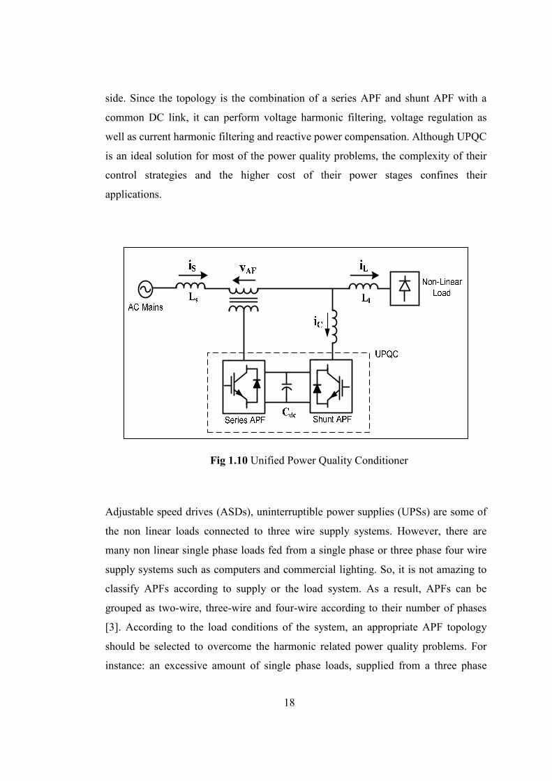
Fig 1.10 Unified Power Quality Conditioner ................................................... 18
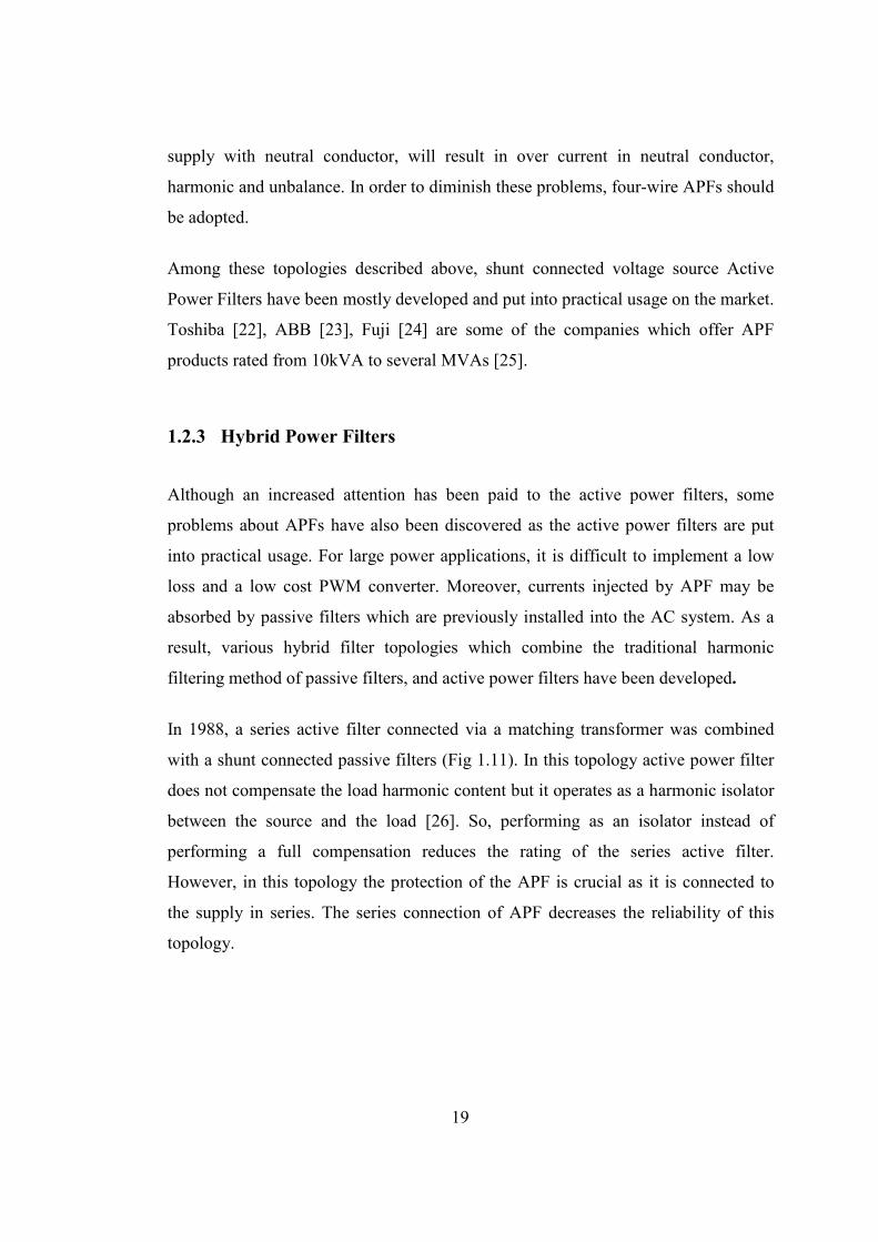
Fig 1.11 Combination of Series APF and Shunt Passive Filter ........................ 20
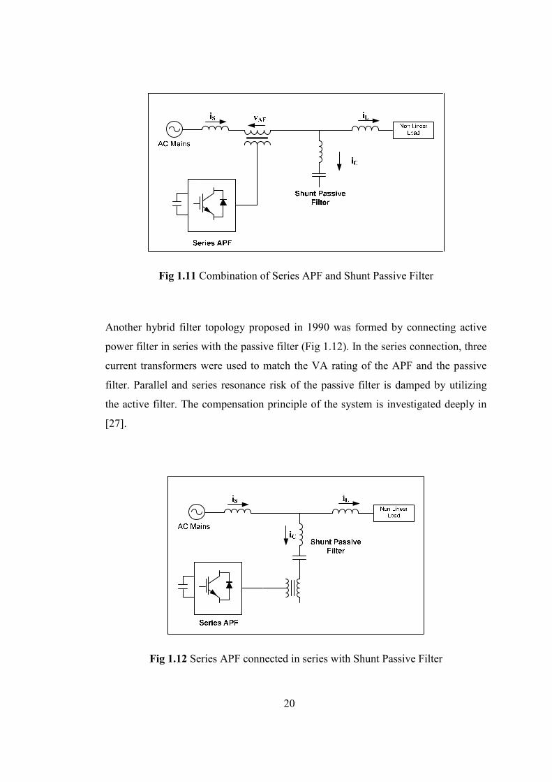
Fig 1.12 Series APF connected in series with Shunt Passive Filter ................. 20
Fig 1.13 Transformerless Shunt Hybrid Power Filter ...................................... 21
Fig 2.1 Transformerless Shunt Hybrid Power Filter ........................................ 26
Fig 2.2 (a) Single Phase Equivalent Circuit (b) Harmonic Equivalent Circuit 27
Fig 2.3 Clarke Transformation and Vector Representation in α-β Frames ...... 32
Fig 2.4 Current Reference Calculation based on p-q Theory ........................... 35
Fig 2.5 (a) Three Phase Current Vectors (b) Clarke Transformation (c) Park
Transformation ..................................................................................... 36
Fig 2.6 Current Reference Calculation Based on SRF Method ........................ 38
Fig 2.7 Block Diagram of the Phase Locked Loop .......................................... 40
Fig 2.8 Single Phase Equivalent Circuit of Hybrid Power Filter ..................... 42
Fig 2.9 Conventional Control Method .............................................................. 44
Fig 2.10 Single Phase Equivalent of Hybrid Power Filter................................ 47
Fig 2.11 Proposed Voltage Feedforward Control Method ............................... 48

xvi
Fig 2.12 Proposed Voltage Reference Generation Method to Exclude
3rd Harmonics..................................................................................... 53
Fig 2.13 Waveform Modulation Method .......................................................... 54
Fig 3.1 Line Current and Voltage (Phase A) .................................................... 56
Fig 3.2 Line Current and Voltage (Phase B) .................................................... 56
Fig 3.3 Line Current and Voltage (Phase C) .................................................... 57
Fig 3.4 Fundamental Component of Line Current
(3 sec. average, Field Data) .................................................................. 57
Fig 3.5 Fundamental Component of Line Current
(15 min. average, Field Data) ............................................................... 58
Fig 3.6 3rd Harmonic Component of Line Current
(3 sec. average, Field Data) .................................................................. 58
Fig 3.7 5th Harmonic Component of Line Current
(3 sec. average, Field Data) .................................................................. 59
Fig 3.8 7th Harmonic Component of Line Current
(3 sec. average, Field Data) .................................................................. 59
Fig 3.9 9th Harmonic Component of Line Current
(3 sec. average, Field Data) .................................................................. 60
Fig 3.10 11th Harmonic Component of Line Current
(3 sec. average, Field Data) ............................................................... 60
Fig 3.11 13th Harmonic Component of Line Current
(3 sec. average, Field Data) ............................................................... 61
Fig 3.12 15th Harmonic Component of Line Current
(3 sec. average, Field Data) ............................................................... 61
Fig 3.13 17th Harmonic Component of Line Current
(3 sec. average, Field Data) ............................................................... 62
Fig 3.14 19th Harmonic Component of Line Current
(3 sec. average, Field Data) ............................................................... 62
Fig 3.15 Simulation Model of the Transformerless Shunt
Hybrid Power Filter ........................................................................... 64

xvii
Fig 3.16 Mains Voltage and Load Current ....................................................... 66
Fig 3.17 Load Current....................................................................................... 67
Fig 3.18 Mains Current Frequency Spectrum (Passive Filter) ......................... 69
Fig 3.19 Mains Current Frequency Spectrum (Hybrid Power Filter) ............... 70
Fig 3.20 Voltage Source Converter .................................................................. 71
Fig 3.21 Simulation Model Used for Conventional Control Method ............... 73
Fig 3.22 Phase Locked Loop (PLL) Output at Steady State ............................ 74
Fig 3.23 During Start Up, Mains Voltage (200V/div), Load Current
(250A/div), Source Current (250A/div), Filter Current (100A/div) ... 75
Fig 3.24 DC Link Voltage Built Up, ................................................................ 75
Fig 3.25 DC Link Voltage (50V/div), Filter Current (100A/div) ..................... 76
Fig 3.26 Hybrid Power Filter Steady State Results with Feedback Control .... 77
Fig 3.27 Hybrid Power Filter Steady State Results with Feedback Control .... 77
Fig 3.28 Hybrid Power Filter Steady State Results with Feedback and ........... 78
Fig 3.29 Hybrid Power Filter Steady State Results with Feedback and ........... 78
Fig 3.30 Frequency Spectrum of Load and Source Current
(Fundamental=305ARMS) .................................................................... 79
Fig 3.31 Supply Current under Different Control Schemes
(FB: Feedback Control, FF: Feedforward Control, VFF: proposed
Voltage Feedforward Control) ............................................................ 82
Fig 3.32 DC Link Voltage Built Up ................................................................. 84
Fig 3.33 DC Link Voltage (20V/div), Filter Current (100A/div) ..................... 84
Fig 3.34 Hybrid Power Filter Steady State Results with Proposed Control ..... 85
Fig 3.35 Hybrid Power Filter Steady State Results with Proposed Control ..... 85
Fig 3.36 Hybrid Power Filter Steady State Results with Proposed Control ..... 86
Fig 3.37 Frequency Spectrum of Load and Mains Current .............................. 86
Fig 3.38 Carrier Wave and Calculated Voltage Reference............................... 87
Fig 3.39 Carrier Wave and Calculated Voltage Reference............................... 88
Fig 3.40 Hybrid Power Filter Steady State Results with Conventional
Control Method, DC Link Voltage (20V/div), Source

xviii
Current (200A/div) ............................................................................. 88
Fig 3.41 Frequency Spectrum of the Source Current with Conventional
Control Method (for different DC link Voltage levels and
Feedback Gains) and with Proposed Control ..................................... 89
Fig 4.1 System Configuration of Hybrid Active Power Filter Prototype ......... 91
Fig 4.2 PM300CLA1200 IPM Module ............................................................. 93
Fig 4.3 Experimental DC Link Capacitor Configuration ................................. 94
Fig 4.4 Experimental Passive Filter Capacitor Configuration .......................... 97
Fig 4.5 Power Stage of the Implemented Hybrid Power Filter Prototype ........ 98
Fig 4.6 Block Diagram of Implemented Control and Protection Circuits ........ 99
Fig 4.7 Signal Measurement Points of Hybrid Power Filter System .............. 100
Fig 4.8 CTF-5A AC Current Sensor ............................................................... 100
Fig 4.9 Control and Protection Circuits of the Implemented Hybrid
Power Filter Prototype ........................................................................ 103
Fig 4.10 Implemented Hybrid Power Filter Prototype ................................... 104
Fig 4.11 Experimental Waveforms when Hybrid Power Filter is OFF .......... 106
Fig 4.12 Frequency Spectrum of Source Current ........................................... 106
Fig 4.13 Experimental Waveforms when only Passive Filter is ON .............. 107
Fig 4.14 Load Current and Source Current when only Passive Filter is ON . 107
Fig 4.15 C1: DC Link Voltage (20V/div), C2: Filter Current (40A/div) ....... 108
Fig 4.16 F1: Load Current (200A/div), C2: Filter Current (40A/div) ............ 109
Fig 4.17 C1: DC Link Voltage (10V/div), C2: Filter Current (40A/div) ....... 109
Fig 4.18 Frequency Spectrum of Load, Source and Filter Current ................ 110
Fig 4.19 Vector Representation of Currents ................................................... 111
Fig 4.20 DC Link Voltage (10V/div), C2: Filter Current (40A/div) .............. 113
Fig 4.21 C2: Filter Current (40A/div), C3: Supply Voltage (100V/div) ........ 114
Fig 4.22 C1: DC Link Voltage (10V/div), C2: Filter Current (40A/div) ....... 114
Fig 4.23 C2: Filter Current (40A/div), C3: Supply Voltage (100V/div) ........ 115
Fig 4.24 Frequency Spectrum of Load, Source and Filter Current ................ 116
Fig 4.25 Single Line Diagram of the Hybrid Power Filter ............................. 116

xix
Fig A.1 Laminated Bus Bar Design and the Power Converter ....................... 134
Fig C.1 Flowchart of the Developed DSP Software ....................................... 139
1
CHAPTER 1
1. INTRODUCTION
In recent years, improvements in power electronics devices and semi-conductor
technology have increased the usage of non-linear loads. Widespread use of non-
linear loads deteriorates the quality of power in both transmission and distribution
systems. The ideal power quality is defined by electrical power energy with pure
sinusoidal supply voltage waveform at a constant frequency and a specified constant
magnitude [1]. Nowadays, the power quality is not only defined by the continuity of
electricity but also characterized by its main parameters. The frequency and
magnitude of the supply voltage, current and voltage harmonics, voltage sags,
voltage swells, flicker and phase imbalances are the main parameters of the power
quality [2]. In today’s environment, electronic loads are very sensitive to harmonics,
sags, swells and other disturbances. So, power quality has become as important as
the continuity of the electricity.
Among these parameters, current and voltage harmonics have become a growing
power quality concern when the undesirable effects on both utility and customer
electronic equipments are considered. Arc furnaces, converters, adjustable speed
drives, static VAR compensators, cylcloconverters, switch mode power supplies and
PWM modulated drives are some of the non-linear loads that generate harmonics.
Voltage distortion, excessive neutral return currents, reduction in equipment lifetime
and overheating of cables, motors and transformers are some of the adverse effects of
harmonics injected by these non-linear loads.
In order to overcome the harmonic related problems, passive filters consisting of
capacitors, inductors and damping resistors have been used for a long time. However,

2
installing conventional passive harmonic filters provide limited solutions to many
power quality problems. Moreover, the risk of the resonance with supply impedance
of the passive filters has increased the attention to active solutions. As a result, active
power filters in various topologies have been studied and reported in the literature
[3].
1.1 Definition of Harmonic Problems
Electrical loads, drawing sinusoidal current from a sinusoidal voltage source, are
called as linear loads. They consist of only resistive (R), inductive (L) and capacitive
(C) passive elements. Whereas, non-linear loads draw non-sinusoidal current
waveform, although they are fed from a sinusoidal voltage source. In order to
indicate the undesirable effects and severity of these non-sinusoidal signals,
harmonic terminology was introduced by Institute of Electrical and Electronics
Engineers (IEEE) in 1981 for these non-sinusoidal signals which can be represented
as the sum of the sinusoidal signals in different frequencies by Fourier series.
According to IEEE Std. 519 [2] reported in 1981, “A sinusoidal component of a
periodic wave or quantity having a frequency that is an integral multiple of the
fundamental frequency is defined as harmonic”.
The increase in the usage of non-linear loads which contain semiconductor switching
devices, has resulted in distorted current and voltage waveforms at the point of
common coupling (PCC) of industrial loads. Some of the most commonly used non-
linear loads and the current drawn from the AC mains are shown below. In Fig 1.1, a
single phase rectifier with smoothing capacitor which supplies most of the single
phase devices (computers, printers, fluorescents, etc.) is indicated. The sharp rising
and falling of line current introduces considerable amount of odd harmonics into the
system.

3
Fig 1.1 Single Phase Rectifier (with Smoothing Capacitor)
Moreover, six-pulse controlled or uncontrolled rectifiers are commonly used in
AC/DC drives and Uninterruptable Power Supply (UPS) applications. Fig 1.2 and
Fig 1.3 shows a six-pulse diode rectifier with a smoothing inductor and capacitor
with their distorted current waveforms. The distorted current introduces harmonics of
the order 5th, 7th, 11th, 13th and so on.
Fig 1.2 Three Phase Diode Rectifier (with Smoothing Reactor)
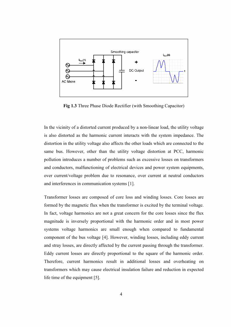
4
Fig 1.3 Three Phase Diode Rectifier (with Smoothing Capacitor) In the vicinity of a distorted current produced by a non-linear load, the utility voltage
is also distorted as the harmonic current interacts with the system impedance. The
distortion in the utility voltage also affects the other loads which are connected to the
same bus. However, other than the utility voltage distortion at PCC, harmonic
pollution introduces a number of problems such as excessive losses on transformers
and conductors, malfunctioning of electrical devices and power system equipments,
over current/voltage problem due to resonance, over current at neutral conductors
and interferences in communication systems [1].
Transformer losses are composed of core loss and winding losses. Core losses are
formed by the magnetic flux when the transformer is excited by the terminal voltage.
In fact, voltage harmonics are not a great concern for the core losses since the flux
magnitude is inversely proportional with the harmonic order and in most power
systems voltage harmonics are small enough when compared to fundamental
component of the bus voltage [4]. However, winding losses, including eddy current
and stray losses, are directly affected by the current passing through the transformer.
Eddy current losses are directly proportional to the square of the harmonic order.
Therefore, current harmonics result in additional losses and overheating on
transformers which may cause electrical insulation failure and reduction in expected
life time of the equipment [5].

5
Additional losses and overheating problems are also experienced by power cables of
an electrical system due to the skin effect. If the cable is subjected to a current
waveform with high frequency harmonics, the AC resistance of conductors increases
with frequency, thus raising the I2R losses. Moreover, unexpected trips on circuit
breakers, malfunctioning of devices using utility voltage as reference, faulty readings
of kWh meters and the telephone interference in communication systems are the
common problems observed in the presence of the harmonics.
Hence, in order to set some practical limitations about harmonics and to offer some
recommendations, a standard named [2] “Guide for Harmonic Control and Reactive
Power Compensation of Static Power Converters” was revealed in 1981 by IEEE
society. After the adverse effects of non linear loads on neighborhood loads had been
discovered, in 1992 the standard was revised and updated [1]. The severity of the
harmonic magnitude is indicated by some quantities such as harmonic factor (HF),
Total Harmonic Distortion (THD), Total Demand Distortion (TDD).
Harmonic factor which is valid for both current and voltage is the ratio of the root
sum square value of all harmonics to the root mean square value of the fundamental
(1.1). It is also called as distortion factor (DF). Moreover, another quantity called
Total Harmonic Distortion (THD) has been used in low-voltage, medium-voltage and
high-voltage systems to extinguish the distortion factor of a voltage or a current
waveform (1.2).
1
2
2
1
2
2
)(
)(
)(
)(
I
I
CurrentFactorHarmonic
V
V
VoltageFactorHarmonic
h
h
h
h
∑
∑
∞
=
∞
=
=
=
(1.1)

6
"":
"":
:
:
%100
)(
)(
1
1
1
50
2
2
horderofcomponentharmoniccurrenttheofAmplitudeI
horderofcomponentharmonicvoltagetheofAmplitudeV
componentcurrentlfundamentatheofvalueRMSI
componentvoltagelfundamentatheofvalueRMSV
xV
V
THDDistortionHarmonicTotal
h
h
h
h
F
∑==
(1.2)
Another THD definition different from statement (1.2) is used by Canadian
Standards Association (CSA) and International Electrotechnical Commission (IEC)
[6]. It defines the THD as a percentage of total RMS including the rms values of all
harmonics (1.3).
"":
:
%100
)(
)(
50
1
2
50
2
2
horderofcomponentharmonictheofAmplitudeV
valueRMSTotalV
VV
xV
V
THDDistortionHarmonicTotal
hRMS
RMS
h
hRMSRMS
RMS
h
h
R
∑
∑
=
=
=
=
(1.3)
Table 1.1 shows the voltage distortion limit values recommended by IEEE 519-1992
at the point of common coupling (PCC). While the voltage distortion limitations are
based on THD values, the current distortion limitations are based on a different
variable as Total Demand Distortion (TDD) which is defined in (1.4).
"":
:
%100
)(
)(
50
2
2
horderofcurrentharmonictheofAmplitudeI
currentloaddemandMaximumI
xI
I
TDDDistortionDemandTotal
h
L
L
h
h∑==
(1.4)
7
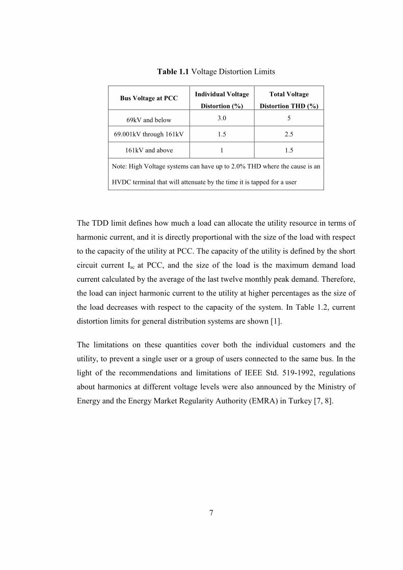
Table 1.1 Voltage Distortion Limits
Bus Voltage at PCC Individual Voltage
Distortion (%)
Total Voltage
Distortion THD (%)
69kV and below 3.0 5
69.001kV through 161kV 1.5 2.5
161kV and above 1 1.5
Note: High Voltage systems can have up to 2.0% THD where the cause is an
HVDC terminal that will attenuate by the time it is tapped for a user
The TDD limit defines how much a load can allocate the utility resource in terms of
harmonic current, and it is directly proportional with the size of the load with respect
to the capacity of the utility at PCC. The capacity of the utility is defined by the short
circuit current Isc at PCC, and the size of the load is the maximum demand load
current calculated by the average of the last twelve monthly peak demand. Therefore,
the load can inject harmonic current to the utility at higher percentages as the size of
the load decreases with respect to the capacity of the system. In Table 1.2, current
distortion limits for general distribution systems are shown [1].
The limitations on these quantities cover both the individual customers and the
utility, to prevent a single user or a group of users connected to the same bus. In the
light of the recommendations and limitations of IEEE Std. 519-1992, regulations
about harmonics at different voltage levels were also announced by the Ministry of
Energy and the Energy Market Regularity Authority (EMRA) in Turkey [7, 8].

8
Table 1.2 Current Distortion Limits for General Distribution Systems (120V through 69kV)
Individual Harmonic Order (Odd Harmonics), h
Isc/ IL Max. Harmonic Current Distortion for h
TDD h<11 11≤h<17 17≤h<23 23≤h<35 35≤h
Below 20
4.0 2 1.5 0.6 0.3 5.0
Between 20-50
7.0 3.5 2.5 1.0 0.5 8.0
Between 50-100
10.0 4.5 4.0 1.5 0.7 12.0
Between 100-1000
12.0 5.5 5.0 2.0 1.0 15.0
Above 1000
15.0 7.0 6.0 2.5 1.4 20.0
Even Harmonics are limited to 25% of the odd harmonics limit above
Current distortions that result in a dc offset, e.g., half wave converters, are not allowed
* All power generation equipment is limited to these values of current distortion, regardless of actual Isc/ IL
Isc= Maximum short circuit current at PCC, IL= Maximum demand load current (fundamental frequency component) at PCC
1.2 Harmonic Mitigation Techniques
A number of solutions exist to reduce the undesirable effects of harmonics. The most
common and the conventional method is installing passive harmonic filters to
remove harmonic currents which present a low cost solution. However, passive filter
implementations to filter out the harmonics have the following disadvantages:
- Possibility of resonances with the source impedance
- Supply impedance dependent system performance
- Fixed compensation characteristic and upgrade difficulty
9
Although enhancements in semiconductor device technology have led to an increase
in the usage of modern harmonic polluter loads, they have also provided reliable
solutions. In order to overcome the problems associated with traditional passive
filters, active power filters (APF) have been worked on and developed in recent years
in conjunction with the improvement in semiconductor switches. In this part, firstly
traditional method of harmonic filtering is briefly discussed. Then, active power filter
history, the basic operation principle of APFs and the classification in the literature
are highlighted. Finally, the hybrid active power filter topology which is the main
concern of this thesis is introduced.
1.2.1 Passive Filters
In order to solve the current harmonic related problems, passive filters consisting of
capacitors, inductors and damping resistors have been used for a long time. They are
used as either to inject a series high impedance to block the harmonic currents, or to
create a shunt low impedance path to divert the harmonic currents path. So, passive
filters are installed either in shunt connection or series connection. While shunt
connected passive filters carry only a fraction of line current, series filters are
subjected to full line current. Moreover, the reactive power compensation capability
of shunt connected passive filters and the lower installation cost of shunt filters make
series passive filters non preferable.
The shunt connected passive filters are classified as band-pass, high pass and C-type
filters. Among these types, low pass and high pass filters are the most common types
due to their design simplicity and low cost [9]. In Fig 1.4 most common types of
shunt passive filters and their circuit configuration is represented.

10
Fig 1.4 Shunt Passive Filters One of the most commonly filter type used in industry for harmonic suppression is
band-pass filters. Although sufficiently low impedance is obtained at a specific
frequency, characteristics of the filter may considerably change with system
parameters. A parallel resonance occurs at frequencies lower than the tuned
frequency. As a result, undesirable harmonic currents can be magnified which
decreases the performance of the overall system [10]. The impedance of a single
tuned filter represented in Fig 1.4 is calculated as follows:
[ ])wC/(1wLjRZfilter −+= (1.5)
Tuning frequency of the filter is defined by the w that results in a zero imaginary part
in (1.5). So the tuning frequency (ftuned) of the filter is given in (1.6).
)LC()(2
1f tuned
π= (1.6)
The initial step for designing a single tuned filter is defining the size of the capacitor
with a reasonable power factor at the operating line voltage. In (1.7), “kVAR filter”
represents the reactive power capacity of the filter and VLL represents the line to line
rated voltage of the filter. Once the size of the capacitor is defined with a reasonable
power factor at the operating line voltage, the reactance value can be calculated by
(1.7).
11
filterkVAR
VX
2
LLc = (1.7)
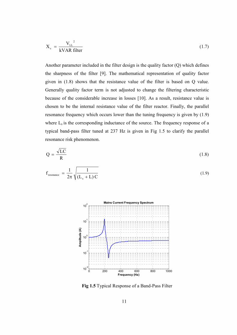
Another parameter included in the filter design is the quality factor (Q) which defines
the sharpness of the filter [9]. The mathematical representation of quality factor
given in (1.8) shows that the resistance value of the filter is based on Q value.
Generally quality factor term is not adjusted to change the filtering characteristic
because of the considerable increase in losses [10]. As a result, resistance value is
chosen to be the internal resistance value of the filter reactor. Finally, the parallel
resonance frequency which occurs lower than the tuning frequency is given by (1.9)
where Ls is the corresponding inductance of the source. The frequency response of a
typical band-pass filter tuned at 237 Hz is given in Fig 1.5 to clarify the parallel
resonance risk phenomenon.
R
LCQ = (1.8)
C)LL(
1
2
1f
s
resonance +π= (1.9)
0 200 400 600 800 100010
-2
10-1
100
101
102
Mains Current Frequency Spectrum
Frequency (Hz)
Amplitude (A)
Fig 1.5 Typical Response of a Band-Pass Filter

12
Another most commonly used filter type for harmonic suppression is high pass
filters. They provide low impedance above a corner frequency. However, the
impedance obtained with a high pass filter in its passband can not be as low as an
impedance value obtained by a single tuned filter at its tuned frequency. The
harmonics of a system can be reduced with a definite percentage above the corner
frequency but large rating of the filter results in high losses at fundamental
frequency. First order high pass filters represented in Fig 1.4 shows higher losses at
fundamental frequency, so first order type high pass filters are rarely used. In
opposite to this, second order high pass filters show less losses at fundamental
frequency when compared with the first order types. Although third order type filters
are the most effective form in the loss performance, their filtering performance is
inferior to that of the second order types.
There exist also C-type filter which is a variation of high pass filter, where the
inductance L is replaced with a series LC circuit tuned at fundamental frequency (Fig
1.4). So, the resonant LC circuit bypasses the resistance at fundamental frequency
thus reduces the losses. C-type filters are generally applied for compensating arc
furnaces and cyclo converters.
Although passive filters have been used for harmonic related problems due to their
installation simplicity, low cost and efficiency, there are some limitations,
restrictions and undesirable effects on the overall system performance as stated
below [11]:
• The system performance is greatly dependent on the supply impedance. Once
passive filters are installed, it is not so easy to change their corner frequency
or size in the vicinity of change in system conditions.
• Resonance may occur between the source impedance and the filter impedance
which results in amplification of harmonics.
• Passive filters have fixed compensation characteristics.

13
• Aging, deterioration and temperature effects may change the tolerances of the
filter components. Therefore, passive filters may result in detuning problem.
As a result, the preceding disadvantages of passive filters have increased the
attention on active power filter solutions.
1.2.2 Active Power Filters
1.2.2.1 History of APFs
The concept of the Active Power Filter and its operation principles were firstly
introduced by H. Sasaki and T. Machida in 1970s [12]. In 1982, an 800 kVA current
source inverter based active power filter was implemented by using GTO thyristors
for the first time in the world [13, 14]. For the proceeding 20 years, the control
strategies of active power filters have been developed [15].
In the early stages of APF implementations, generally power MOSFETs and GTOs
were utilized. However, the real improvement in APF technology has appeared with
the introduction of insulated gate bipolar transistors (IGBTs). Moreover the progress
in digital signal processors (DSPs), field programmable gate arrays (FPGAs) and
availability of Hall Effect sensors and isolation amplifiers at low cost have forced
researchers and designers to develop efficient control strategies for the APFs to solve
harmonic related problems in the utility and industrial power systems.
The operation principle of APFs is basically canceling the distorting harmonic
currents by measuring them and generating a harmonic current spectrum in opposite
phase to the measured current. As shown in Fig 1.6, the parallel active power filter is
considered as a current source injecting harmonic current into the ac system with the
same amplitude and in anti-phase that of the load current to obtain an undistorted
sinusoidal source current.

14
Fig 1.6 Main Principle of Active Filtering The compensation currents are generated via a pulse width modulated (PWM)
converter including a DC link energy storage element (DC Link Capacitor or DC
Link Inductor) depending on the employed converter type. No additional DC supply
is required for the DC link side; because a small amount of current at fundamental
frequency is drawn from the supply to meet the APF losses so that the DC link
voltage or current is kept constant. In addition to their basic principle of harmonic
current compensation, active power filters are also used for elimination of voltage
harmonics, reactive power compensation and load balancing depending on the type
of the APF. There exist several active power filter types in the literature in
accordance with their converter types, circuit topologies and number of phases [3].
1.2.2.2 Classification of Active Power Filters
Active power filters are divided into two groups according to their converter types
used in the development of the power circuit, as Current Source Converter (CSC)
and Voltage Source Converter (VSC) type active power filters. The main difference
between these two topologies is the energy storage element at the DC link side of the
converter.
15
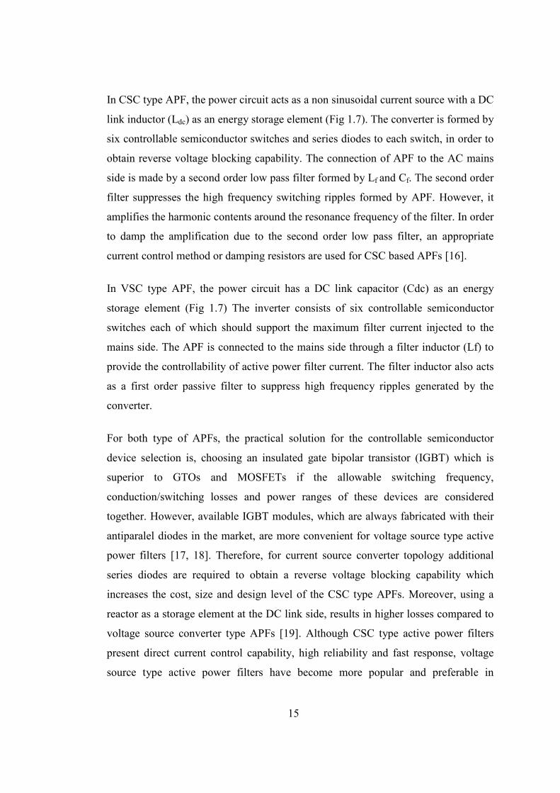
In CSC type APF, the power circuit acts as a non sinusoidal current source with a DC
link inductor (Ldc) as an energy storage element (Fig 1.7). The converter is formed by
six controllable semiconductor switches and series diodes to each switch, in order to
obtain reverse voltage blocking capability. The connection of APF to the AC mains
side is made by a second order low pass filter formed by Lf and Cf. The second order
filter suppresses the high frequency switching ripples formed by APF. However, it
amplifies the harmonic contents around the resonance frequency of the filter. In order
to damp the amplification due to the second order low pass filter, an appropriate
current control method or damping resistors are used for CSC based APFs [16].
In VSC type APF, the power circuit has a DC link capacitor (Cdc) as an energy
storage element (Fig 1.7) The inverter consists of six controllable semiconductor
switches each of which should support the maximum filter current injected to the
mains side. The APF is connected to the mains side through a filter inductor (Lf) to
provide the controllability of active power filter current. The filter inductor also acts
as a first order passive filter to suppress high frequency ripples generated by the
converter.
For both type of APFs, the practical solution for the controllable semiconductor
device selection is, choosing an insulated gate bipolar transistor (IGBT) which is
superior to GTOs and MOSFETs if the allowable switching frequency,
conduction/switching losses and power ranges of these devices are considered
together. However, available IGBT modules, which are always fabricated with their
antiparalel diodes in the market, are more convenient for voltage source type active
power filters [17, 18]. Therefore, for current source converter topology additional
series diodes are required to obtain a reverse voltage blocking capability which
increases the cost, size and design level of the CSC type APFs. Moreover, using a
reactor as a storage element at the DC link side, results in higher losses compared to
voltage source converter type APFs [19]. Although CSC type active power filters
present direct current control capability, high reliability and fast response, voltage
source type active power filters have become more popular and preferable in

16
industrial applications due to their small size, lower initial cost and higher
efficiencies.
Fig 1.7 APF Converter Classification (a) Current Source Converter type APF (b) Voltage Source Converter type APF
Active power filters are also classified as shunt (parallel) APF, series APF, unified
power quality conditioners (UPQC) and hybrid filters according to their topologies
[13]. Shunt APFs are widely used for eliminating load current harmonics and
reactive power compensation. Both of the filters represented in Fig 1.7 are shunt
active power filters.
Fig 1.8 shows the connection of a series APF which is usually used for eliminating
voltage harmonics and regulating voltage at the load or line terminal [20]. The
operation principle is the dual of the shunt connected active power filters (Fig 1.6).
In this case, APF injects a voltage term (VAF) in series with the utility voltage to
operate as a harmonic isolator between the load and utility or to operate as a voltage
regulator (Fig 1.9). Moreover, in many cases series active power filters are combined
with shunt passive filters in order to decrease the rated power of the APF [21].

17
Fig 1.8 Series Active Power Filter
Fig 1.9 Operation Principle of Series APF Another type of APF which combine the series and shunt active filters is developed
as unified power quality conditioners (UPQC). As indicated in Fig 1.10, the shunt
connected part is located at the load side and the series part is located at the source
18
side. Since the topology is the combination of a series APF and shunt APF with a
common DC link, it can perform voltage harmonic filtering, voltage regulation as
well as current harmonic filtering and reactive power compensation. Although UPQC
is an ideal solution for most of the power quality problems, the complexity of their
control strategies and the higher cost of their power stages confines their
applications.
Fig 1.10 Unified Power Quality Conditioner Adjustable speed drives (ASDs), uninterruptible power supplies (UPSs) are some of
the non linear loads connected to three wire supply systems. However, there are
many non linear single phase loads fed from a single phase or three phase four wire
supply systems such as computers and commercial lighting. So, it is not amazing to
classify APFs according to supply or the load system. As a result, APFs can be
grouped as two-wire, three-wire and four-wire according to their number of phases
[3]. According to the load conditions of the system, an appropriate APF topology
should be selected to overcome the harmonic related power quality problems. For
instance: an excessive amount of single phase loads, supplied from a three phase
19
supply with neutral conductor, will result in over current in neutral conductor,
harmonic and unbalance. In order to diminish these problems, four-wire APFs should
be adopted.
Among these topologies described above, shunt connected voltage source Active
Power Filters have been mostly developed and put into practical usage on the market.
Toshiba [22], ABB [23], Fuji [24] are some of the companies which offer APF
products rated from 10kVA to several MVAs [25].
1.2.3 Hybrid Power Filters
Although an increased attention has been paid to the active power filters, some
problems about APFs have also been discovered as the active power filters are put
into practical usage. For large power applications, it is difficult to implement a low
loss and a low cost PWM converter. Moreover, currents injected by APF may be
absorbed by passive filters which are previously installed into the AC system. As a
result, various hybrid filter topologies which combine the traditional harmonic
filtering method of passive filters, and active power filters have been developed.
In 1988, a series active filter connected via a matching transformer was combined
with a shunt connected passive filters (Fig 1.11). In this topology active power filter
does not compensate the load harmonic content but it operates as a harmonic isolator
between the source and the load [26]. So, performing as an isolator instead of
performing a full compensation reduces the rating of the series active filter.
However, in this topology the protection of the APF is crucial as it is connected to
the supply in series. The series connection of APF decreases the reliability of this
topology.
20
Fig 1.11 Combination of Series APF and Shunt Passive Filter Another hybrid filter topology proposed in 1990 was formed by connecting active
power filter in series with the passive filter (Fig 1.12). In the series connection, three
current transformers were used to match the VA rating of the APF and the passive
filter. Parallel and series resonance risk of the passive filter is damped by utilizing
the active filter. The compensation principle of the system is investigated deeply in
[27].
Fig 1.12 Series APF connected in series with Shunt Passive Filter

21
Both of the topologies represented in Fig 1.11 and Fig 1.12 include an active power
filter, passive filter and a three phase transformer. Comparison between their
compensation performance, filtering characteristics and reliabilities can be found in
[28]. Existence of a transformer in the circuit topology inevitably increases the cost
of the system which makes the topology non preferable. As a result, a shunt hybrid
power filter topology named transformerless hybrid filter was proposed which uses a
single LC passive filter for each phase and a small rated voltage source converter
based active power filter [29]. The series connection between the LC passive filter
and the voltage source converter is completed without using any matching
transformer (Fig 1.13).
Fig 1.13 Transformerless Shunt Hybrid Power Filter
1.3 Scope of the Thesis
In recent years, harmonic pollution has become a growing problem in transmission
and distribution systems, due to the non-linear loads used in industrial and domestic
applications. So far, shunt passive filters have been preferred to suppress harmonics
due to their low cost and efficiency. However, resonance risk with the supply

22
impedance, source impedance dependent performance, fixed compensation
characteristics of passive filters discourage their applications. As a result, active
power filters have been developed by utilizing PWM converters in various
configurations and topologies to overcome the drawbacks of passive filters.
In addition to elimination of current and voltage harmonics, APFs have reactive
power compensation and load balancing capabilities depending on the utilized
topology. Among the topologies listed in the literature, conventional shunt connected
voltage source converter type APF is widely used in industrial applications.
However, for high power applications the rating and the losses of power converter
increase considerably. Furthermore, in order to connect the APF system to the utility,
a step down transformer is required which increase the initial cost of the system.
Therefore another approach called Hybrid Active Power Filters to mitigate
harmonics has been developed. Hybrid power filter topologies are formed by using a
low cost passive filter and a low rated APF. In fact, hybrid power filters are used to
improve the compensation characteristics of passive filters. The approach eliminates
the drawbacks of pure active power filters and pure passive filters while keeping the
advantages of both.
In this thesis, a shunt connected transformerless Hybrid Power Filter formed by the
use of a low rated three phase voltage source PWM converter and a series connected
LC passive filter, is designed and implemented. The laboratory prototype is designed
to eliminate the most dominant harmonics existing at TÜBĐTAK-SPACE
Technologies Institute 400V bus. The existing 5th, 7th and 11th harmonics are greatly
reduced to satisfy the IEEE Std.519 current distortion limits. It is shown that the
required DC link voltage for the system is quite low when compared with a pure
voltage source type Active Power Filter. However, the usage of series connected
passive filter in the hybrid filter topology results in unavoidable fundamental leading
current flow. Furthermore, the reactive power compensation capability of the
implemented hybrid power filter is fixed due to its topology which is the main
disadvantage of the implemented system.

23
Moreover, the effectiveness of the control method given in [29] for the
transformerless hybrid power filter is investigated. The undesirable effects of the
supply side voltage harmonics are stated and a contribution to the control method by
utilizing supply voltage is presented by simulation results. Actually, the current
harmonic content of the experimental load includes not only 5th, 7th and 11th
harmonics but also unbalanced 3rd harmonic due to the fluorescent lamps and single
phase rectifiers. So, current references obtained in the indicated control method [29]
also includes 3rd harmonic. However, the designed hybrid power filter system has a 3
phase-3 wire connection and it is not possible to eliminate these 150Hz components
with this configuration [3, 30-31]. In fact, the existence of third harmonics and its
undesirable effects on conventional control method are discovered during the
experimental tests of this thesis work. Since the power stage of the prototype has
been already designed and mounted, a neutral point connection modification could
not be performed. As a result, the problem is solved by modifying the current
harmonic reference calculation method. The most dominant harmonic content of the
load is calculated individually for each harmonic frequency but by excluding 3rd
harmonic component. The advantages of the designed system and the proposed
current reference calculation methods are verified by both simulation and
experimental results. The outline of the thesis is as given below:
In Chapter 2, circuit topology and the operating principle of the transformerless
hybrid power filter is described. First, circuit configuration of the system and the
principles of harmonic filtering are stated. Then, methods utilized in the control
system for the calculation of current references are described. Thirdly, the most
common control method preferred for transformerless hybrid power filter is
introduced and analyzed. The undesirable effects of the supply side voltage
harmonics are stated and a feed forward control loop is proposed. Finally, in order to
exclude the 150Hz components of the load current from the compensation current
references of the active filter, the proposed reference generation method is described.
The applied modulation method to obtain the appropriate switching signals of
semiconductor devices is also presented at the end of this Chapter.

24
In Chapter 3, the design procedure of the hybrid active power filter system is given,
by means of simulation results. After showing the measurement results, obtained at
400V low voltage bus of TÜBĐTAK, the non-linear load model of the system is
obtained. Then, the circuit elements of the system are designed and selected in terms
of their current and voltage ratings. After defining the system parameters, the
theoretical results and the performance of the system are shown for the conventional
control method and the proposed reference generation method by utilizing
EMTDC/PSCAD program.
In Chapter 4, the implementation of 4.7 kVA hybrid active power filter and
experimental results are presented. First, the power stage of the laboratory prototype
which includes power converter, DC link side and passive filter elements are given.
Secondly, control and protection circuits of the system are stated. After discussing
the software structure of the implemented system, effectiveness of the proposed
control method is confirmed by experimental results.
General conclusions are given in Chapter 5. In the same chapter further work
proposals are also discussed.
In Appendix A, electrical characteristics of the Intelligent Power Module (IPM),
technical specifications of the utilized DC link capacitor and passive filter reactor are
given. Moreover, laminated bus bar design of the power converter is demonstrated in
this part.
In Appendix B, technical data of the employed AC current sensor, the voltage
transducer, 220VAC/24VDC power supply and the digital signal processor (DSP) are
presented.
In Appendix C, flowchart of the developed DSP software is given.

25
CHAPTER 2
2 TRANSFORMERLESS SHUNT HYBRID POWER
FILTER
2.1 Circuit Topology
Shunt hybrid power filter which is the main concern of this research work is formed
by the use of a three phase voltage source PWM converter, and a series connected
LC passive filter. The series connection between the passive filter and the voltage
source converter is made directly, without using a transformer (Fig 2.1). The series
connected LC filter is tuned to dominant harmonic component of the load. It absorbs
the current harmonics arising from the non-linear load; however, the filtering
characteristic of just the passive filter itself is not satisfactory. Hence, active power
filter is used to improve the filtering performance of the overall system and to
suppress the resonance risk of the passive filter.
The power circuit of the inverter includes an energy storage element of a DC link
capacitor and controllable semiconductor switches with their antiparalel diodes.
Active power filter injects compensation currents by operating as a current controlled
voltage source. In conventional voltage source active power filter topology (Fig 1.7),
the DC link capacitor voltage is required to be higher than the peak value of the
utility voltage; otherwise the generated compensation currents cannot be injected to
the mains [32, 33]. However, the presence of filter capacitor in this topology (Fig
2.1) ensures a reduced DC link voltage and a low rated voltage source converter at
the expense of additional fundamental current, passing through the converter [34]. As
a result, for low voltage applications, PWM converter can be formed by power
MOSFETs instead of using IGBTs. So that, the initial cost of the converter can be
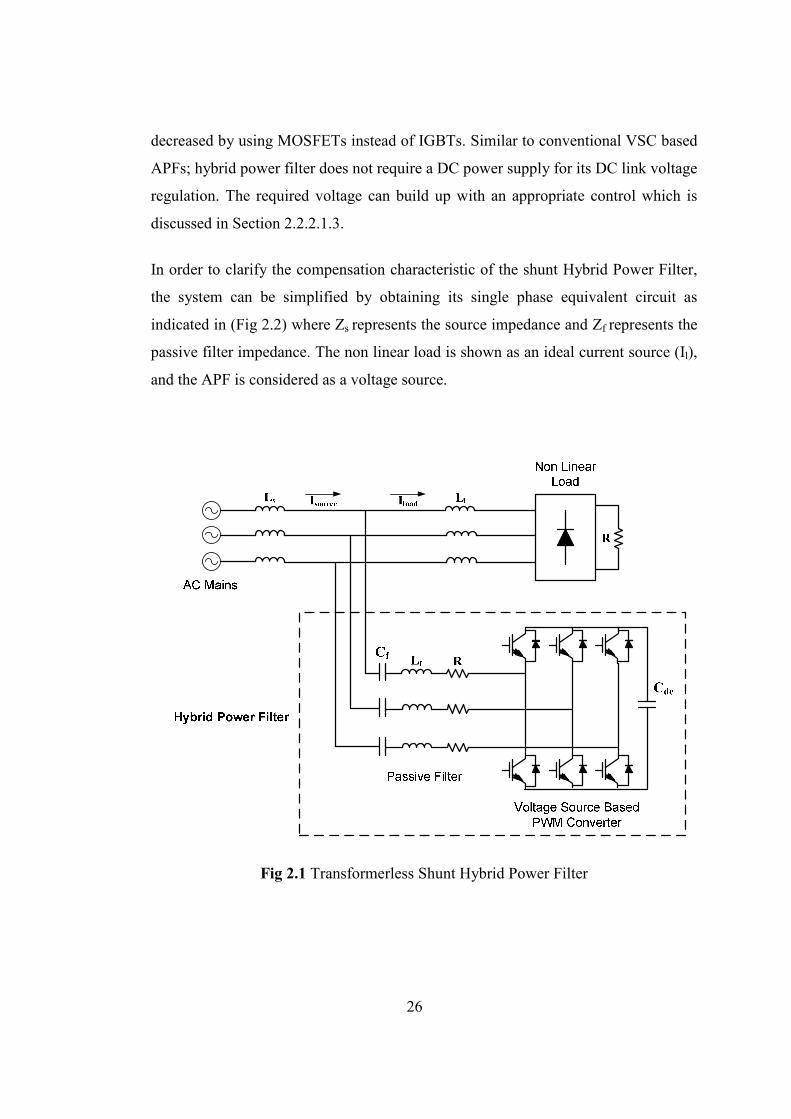
26
decreased by using MOSFETs instead of IGBTs. Similar to conventional VSC based
APFs; hybrid power filter does not require a DC power supply for its DC link voltage
regulation. The required voltage can build up with an appropriate control which is
discussed in Section 2.2.2.1.3.
In order to clarify the compensation characteristic of the shunt Hybrid Power Filter,
the system can be simplified by obtaining its single phase equivalent circuit as
indicated in (Fig 2.2) where Zs represents the source impedance and Zf represents the
passive filter impedance. The non linear load is shown as an ideal current source (Il),
and the APF is considered as a voltage source.
Fig 2.1 Transformerless Shunt Hybrid Power Filter

27
I sh
IfhI s
If
Fig 2.2 (a) Single Phase Equivalent Circuit (b) Harmonic Equivalent Circuit If the active power filter terminal voltage is assumed to have no fundamental
component, voltage across the PWM inverter can be represented as K x Ish at
harmonic frequencies where ‘h’ stands for the harmonic components and K
represents the feedback gain which is described in Section 2.2.2.1.1. Hence,
assuming the source voltage to be pure 50Hz and considering the current directions
as in Fig 2.2, the following equations can be obtained by applying Kirchhoff’s
voltage law.
shafsh
affhfhshshsh
KIVand0V
;where
0VZIZIV
==
=−−−
(2.1)
fhlhsh III += (2.2)
Combine (2.1) and (2.2);
KZZ
ZI
shfh
fhsh ++= (2.3)
Equation (2.3) indicates that as the active power filter is connected to the system,
feedback gain K acts as a damping resistor which suppresses the resonance between
the supply and the passive filter. Theoretically, as K approaches to infinity, the

28
harmonic content of the source current goes towards zero. However due to stability
problems in the control loop, the gain K should be limited to certain values [29, 35].
Hence the design procedure of transformerless shunt hybrid filter can be divided into
2 groups as the design of the passive filter and the design of the active filter part. The
design of the passive filter is mainly identifying the Lf, Cf parameters considering the
harmonic content of the load. It is clear that, tuning frequency of the passive filter is
chosen to be the most dominant harmonic component of the non linear load. Today’s
industrial loads generally consist of three phase diode rectifiers as AC/DC converters
instead of PWM converters due to their low cost and efficiencies. As a result, in the
case of a diode rectifier, the passive filter should be adjusted to eliminate the 5th or
7th harmonic current content.
Although the 5th harmonic current content of a diode rectifier is higher than its 7th
harmonic components, it is more reasonable to tune the passive filter around 350Hz.
An LC filter tuned at 350 Hz shows lower impedance at 550Hz and 650 Hz than a
passive filter tuned at 250 Hz. So it has better filtering characteristics when 11th and
13th harmonics are taken into account. Moreover, for the same value of a filter
inductor (Lf), the capacitor required for a 7th harmonic filter is less bulky than that of
a 5th harmonic filter. An LC passive filter tuned at 350 Hz amplifies the 5th harmonic
current components at the mains side; however, it can be suppressed by the active
power filter with the applied feedback and feedforward control explained in Section
2.2.2.1 [29, 34-35].
2.2 Control Techniques and Modulation Methods
In transformerless hybrid filter topology, PWM converter generates compensation
voltages by operating as a current controlled voltage source. So, the performance of
the system is highly dependent on the accurate measurement and the calculation of
the compensation current references. Once the current references are obtained,
29
voltage reference for each phase is produced by an appropriate control method in
which the gate signals of semiconductor switches are also produced in modulation
part.
2.2.1 Calculation of Current References
Current reference generation methods are classified as time domain or frequency
domain methods in the literature [36-42]. Discrete Fourier Transform (DFT), Fast
Fourier Transform (FFT), Recursive Discrete Fourier Transform (RDFT), Kalman
filter are the methods developed in frequency domain. Before 1990’s, FFT is the
most popular method which defines the amplitude and the phase information of the
sampled current/voltage over a period. However, as the order and the number of
harmonics to be compensated increases, the number of calculations increases as well.
Therefore, increased computational requirement and the longer response time have
turned the attention towards time domain calculations.
Instantaneous reactive power (p-q) theory and synchronous reference frame (SRF)
method are the most common and widely used time domain methods for current
reference calculations. They have faster responses to rapid changes in power system,
and require less computation as compared with the frequency domain methods.
Moreover, the development in digital signal processors allows designers to make
easy and effective implementations. In this thesis, both in simulation and
implementation procedures of 400V Hybrid Power Filter prototype, synchronous
reference frame method is utilized to extract the harmonic content of the load. In this
section instantaneous reactive power theory is also described.
2.2.1.1 Instantaneous Reactive Power (p-q) Theory
Early calculations related with the power flow of electrical systems were based on
the average power or rms values of voltage and current. In 1982, a new concept was
30
defined by H. Akagi, called instantaneous reactive power (p-q) theory in the journal
transactions of IEEE Japan [43]. Then the new concept had also been verified
experimentally that the theory is suitable and efficient to design controllers for the
power conditioners including power electronic devices [44, 45].
The p-q theory is based on the definitions of instantaneous active and reactive
powers in the time domain by using instantaneous voltage and current components
on αβ0 coordinates. So the p-q theory first utilizes Clarke Transformation to map
three phase instantaneous voltages and line currents into αβ0 axes. Transformation
matrices C and C-1 for Clarke transformation and inverse Clarke transformation are
given respectively in (2.4) and (2.5).
−
−−=
=
β
α
c
b
a
c
b
a0
V
V
V
2
3
2
30
2
1
2
11
2
1
2
1
2
1
3
2
V
V
V
C
V
V
V
(2.4)
−−
−=
=
β
α
β
α−
V
V
V
2
3
2
1
2
1
2
3
2
1
2
1
012
1
3
2
V
V
V
C
V
V
V 00
1
c
b
a
(2.5)
Equations are given for voltage vectors but they are also valid for current vectors.
The subscript “0” denotes the zero sequence components either in current or voltage.
In a three phase three wire system, no zero sequence current can flow and if the
phase voltages are balanced, no zero sequence voltage can exist even if the system is
three phase four wire. For simplicity, the zero sequence terms in (2.4) and (2.5) are
eliminated to show the α-β axes mapping of a three phase balanced linear system.
31
Instantaneous phase voltages and line currents in abc axes are given in (2.6) and
(2.7).
)3
2wtcos(V2)t(V
)3
2wtcos(V2)t(V
)wtcos(V2)t(V
Vc
Vb
Va
π+φ+=
π−φ+=
φ+=
(2.6)
)3
2wtcos(I2)t(i
)3
2wtcos(I2)t(i
)wtcos(I2)t(i
Ic
Ib
Ia
π+φ+=
π−φ+=
φ+=
(2.7)
Substitute (2.6) and (2.7) in (2.4);
)cos(3
))3
2cos(
2
2)
3
2cos(
2
2)cos(2(
3
2
V
VVV
wtV
wtVwtVwtVV
φ
πφ
πφφα
+=
++−−+−+= (2.8)
)sin(3
))3
2cos(
2
3)
3
2cos(
2
3(
3
2
V
VV
wtV
wtVwtVV
φ
πφ
πφβ
+=
++−−+= (2.9)
Similarly,
)sin(3
)cos(3
I
I
wtIi
wtIi
φ
φ
β
α
+=
+= (2.10)
Then, a voltage vector ‘e’ and a current vector ‘i’ (2.11) are defined on α-β reference
frames using (2.8), (2.9), and (2.10). So, the graphical representations after abc to α-
β transformation for the obtained voltage and current vectors in α-β reference frames
are as indicated in Fig 2.3.

32
)wt(jII
)wt(jVV
I
V
eI3)wtsin(j)wt(cos(I3jiii
eV3)wtsin(j)wt(cos(V3jVVe
φ+βα
φ+βα
=φ++φ+=+=
=φ++φ+=+= (2.11)
Fig 2.3 Clarke Transformation and Vector Representation in α-β Frames Instantaneous complex power (S) is defined as the multiplication of the voltage
vector ‘e’ and the complex conjugate of the current vector ‘i*’ as given in (2.12).
)iViV(j)iViV(
)jii()jVV(ieS *
βαβββαα
βαβα
α−++=
−+=⋅= (2.12)
p q
A matrix form of (2.12) can be obtained as follows:
−=
β
α
αβ
βα
i
i
VV
VV
q
p (2.13)
Rearranging (2.13);
−+=
αβ
βα
βαβ
α
q
p
VV
VV
VV
1
i
i22
(2.14)

33
q~qq
p~pp
+=
+= (2.15)
Where p is the instantaneous real power, q is the imaginary reactive power. The real
and imaginary power terms include only constant values for the derivations indicated
above. However if the load is non-linear, the current vector will include not only the
fundamental frequency component but also the harmonics, depending on the order.
Then the instantaneous real and imaginary powers will have a dc component and an
oscillating component as decomposed in (2.15). The average (dc) components of
both active and reactive power terms in the system are represented with an over bar
sign (-) and the oscillating parts are represented by an over tilde (~) sign. The
oscillating part of the active power ( p~ ) which has a zero mean is an additional
power flow without a contribution to the energy transfer from source to load.
Moreover, the oscillating part of the imaginary power ( q~ ) stands for the power
exchanged between the phases which has no effect on the energy transfer between
the source and the load.
However if zero sequence terms exist in the system, simplified transformations and
equations are not applicable. If zero sequence voltage and current both appear,
another instantaneous power term p0 (zero sequence power) is introduced. Assume
three phase voltages and currents consist of positive and zero sequence terms (2.16),
(2.17).
)wtsin(V2)3
2wtsin(V2)t(V
)wtsin(V2)3
2wtsin(V2)t(V
)wtsin(V2)wtsin(V2)t(V
0V0Vc
0V0Vb
0V0Va
φ++π
+φ+=
φ++π
−φ+=
φ++φ+=
+
+
+
(2.16)

34
)wtsin(I2)3
2wtsin(I2)t(i
)wtsin(I2)3
2wtsin(I2)t(i
)wtsin(I2)wtsin(I2)t(i
0I0Ic
0I0Ib
0I0Ia
φ++π
+φ+=
φ++π
−φ+=
φ++φ+=
+
+
+
(2.17)
Applying C matrix given in (2.4);
)wtsin(V6V
)wtcos(V3V
)wtsin(V3V
0V00
V
V
φ+=
φ+=
φ+=
++β
++α
(2.18)
)wtsin(I6i
)wtcos(I3i
)wtsin(I3i
0I00
i
i
φ+=
φ+=
φ+=
++β
++α
(2.19)
By utilizing (2.12), real, imaginary and zero sequence power terms are obtained as
given in (2.20) and (2.21).
−
=
β
α
αβ
βα
i
i
i
VV
VV
V
q
p
p 000
0
0
00
(2.20)
00000000000~)2cos(3)cos(3 ppwtIVIVp iViV +=++−−= φφφφ (2.21)
Real and imaginary powers indicated in (2.21) are similar to previous analysis
described above since they depend only on positive sequence components of voltage
and the current. The zero sequence power (p0) has an average value and an
oscillating part at twice the line frequency. It has no contribution to the real power p
or the imaginary power q. The average value of the zero sequence power represents a
unidirectional energy flow and oscillating part is responsible for instantaneous
energy transfer.

35
It can be concluded that; p-q theory is based on the definitions of real, imaginary and
zero sequence power terms by using instantaneous voltage and current components
on αβ0 coordinates. The three phase instantaneous active power which corresponds
to the total energy flow per unit time is the sum of the real power p and the zero
sequence power p0. However, imaginary power does not contribute to the energy
transfer; it represents the energy being exchanged between the phases of the system.
It is reasonable to select the undesirable power components for compensators by
using p-q theory. In the case of a non-linear load, the compensating current
references of an active filter can be produced by selecting the appropriate power
references after utilizing the instantaneous power theory [46]. For instance, if the
active power filter is to be designed only for harmonic current compensation without
any reactive power compensation, the oscillating parts of p and q should be selected
as a power reference. The oscillating parts can be extracted with a high pass filter
(HPF) and utilizing equation (2.13), (2.14) and inverse Clarke transformation
respectively yields the desired compensation current references (iCa*, iCb
*, iCc*) in abc
coordinates (Fig 2.4).
Fig 2.4 Current Reference Calculation based on p-q Theory
2.2.1.2 Synchronous Reference Frame Method
Synchronous reference frame method is based on the transformation of vectors into
synchronously rotating direct (d), and quadrature axis (q) reference frames. In order
to calculate the harmonic components of the mains current, initially three phase
supply current vectors are mapped into stationary α-β axes by utilizing Clarke
36
Transformation (2.4). Then, vectors in stationary reference frame are transformed
into synchronously rotating reference frame by utilizing Park transformation.
Transformation matrices P and P-1 for Park transformation and inverse Park
transformation are given respectively in (2.22) and (2.23). The phase angle θ
represented in Park transformation defines the fundamental frequency phase
information of the utility voltage and it is obtained from a phase locked loop circuit
which is investigated in 2.2.2.1.1.
−=
=
β
α
β
α
θθθθ
i
i
i
iP
i
i
q
d
)cos()sin(
)sin()cos( (2.22)
−=
=
−
q
d
q
d
i
i
i
iP
i
i
)cos()sin(
)sin()cos(1
θθθθ
β
α (2.23)
Once the current vectors are transformed into synchronously rotating d-q reference
frame, the fundamental component of the mains current turns out to be a DC signal,
and the harmonic components which are still AC signals are rotating with a
corresponding angular frequency.
Fig 2.5 (a) Three Phase Current Vectors (b) Clarke Transformation (c) Park Transformation

37
For instance; 5th and 7th harmonic components of a distorted source current turns out
to be a 300Hz signal for a 50Hz AC mains. Since the rotation angle of the reference
frame is positive, positive and negative sequence harmonic components are
transformed to 300Hz and its multiples in synchronous d-q reference frame [40-42,
47, 48]. Therefore, the method is specifically named as positive sequence SRF
method.
AC signals are extracted via a high pass filter (HPF) or by subtracting the DC
quantity obtained from a low pass filter (1-LPF). Low pass filters with low cut off
frequencies (20Hz-30Hz) are sufficient to extract the DC component. Since the
extracted signal is a DC quantity, SRF method is insensitive to phase errors
introduced by the filters. Inverse transformation of the obtained AC signals
reproduces the supply harmonic current components in stationary abc frame.
If the supply voltage is not balanced and the source current contains fundamental
negative sequence component, it turns out to be a 100Hz component in synchronous
d-q reference frame, and it is not extracted by the LPF. Therefore, fundamental
negative sequence component appears in the references of the active power filter.
However, utilizing negative sequence SRF method, in which the vectors are
produced by -θ, prevents the appearance of fundamental negative sequence
component in the reference currents of the APF [47]. The method is similar to the
positive sequence SRF. The current vectors are transformed into negative sequence
d-q reference frame. In this case fundamental negative sequence current component
turns out to be a DC signal and extracted via a LPF. The extracted DC signal is back
transformed into stationary α-β reference frame, and subtracted from the references
of the positive sequence SRF method in α-β reference frame. Current reference
calculation including positive and negative sequence SRF method is summarized in
Fig 2.6.
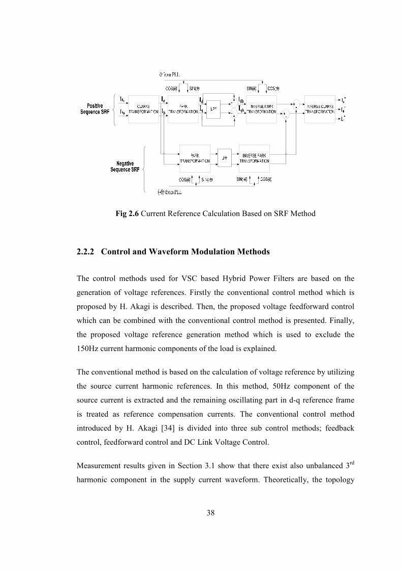
38
Fig 2.6 Current Reference Calculation Based on SRF Method
2.2.2 Control and Waveform Modulation Methods
The control methods used for VSC based Hybrid Power Filters are based on the
generation of voltage references. Firstly the conventional control method which is
proposed by H. Akagi is described. Then, the proposed voltage feedforward control
which can be combined with the conventional control method is presented. Finally,
the proposed voltage reference generation method which is used to exclude the
150Hz current harmonic components of the load is explained.
The conventional method is based on the calculation of voltage reference by utilizing
the source current harmonic references. In this method, 50Hz component of the
source current is extracted and the remaining oscillating part in d-q reference frame
is treated as reference compensation currents. The conventional control method
introduced by H. Akagi [34] is divided into three sub control methods; feedback
control, feedforward control and DC Link Voltage Control.
Measurement results given in Section 3.1 show that there exist also unbalanced 3rd
harmonic component in the supply current waveform. Theoretically, the topology

39
used in this thesis is not suitable to eliminate these components without the neutral
wire connection [3, 30-31]. So, a reference generation method which is based on the
calculation of voltage reference for each dominant harmonic frequency individually
is proposed. Finally, the obtained voltage references are compared with a carrier
wave to obtain the gate signals of the semiconductors.
2.2.2.1 Conventional Control Method
2.2.2.1.1 Feedback Control
In feedback control, synchronous reference frame method is used to calculate the
harmonic components of the mains current. Three phase supply current vectors are
transformed into d-q frames rotating at the fundamental frequency w1 by applying
Clarke and Park transformations as described in Section 2.2.1.2 (Fig 2.5). In Park
transformation, the phase angle (θ) of the supply voltage is required which affects the
performance of the control method. Hence, an accurate phase tracking system is the
key point of the control method to transform the measured current vectors into
synchronously rotating d-q reference frame. In this research work, a phase locked
loop system given in (Fig 2.7) is utilized both in theoretical and experimental works
[49, 50].

40
θ
s
KK IP +
s
1 θ
Fig 2.7 Block Diagram of the Phase Locked Loop
The phase tracking system indicated above includes the transformation of utility
voltages into d-q reference frame and a PI controller. The system is a closed loop
controller in which the transformation of the utility voltage is performed by using the
θ output of the PI controller.
Assume that, the three phase balanced utility voltages are as follows:
+
−=
)3
2sin(
)3
2sin(
)sin(
πϕ
πϕ
ϕ
M
SC
SB
SA
V
V
V
V
(2.24)
Applying TS and P (θ), utility voltage can be expressed in stationary (α-β) and
synchronous (d-q) reference frames respectively as given in (2.25) and (2.26)
−=
=
3
)( SBSC
SA
SC
SB
SA
S VV
V
V
V
V
TV
V
β
α (2.25)

41
Where,
−−
−−
=
2
3
2
31
2
1
2
11
3
2ST
)cos(3
)()cos()sin(
)sin(3
)()sin()cos(
θϕθθ
θϕθθ
−=−
×+×=
−=−
×−×=
M
SBSC
SAqe
MSBSC
SAde
VVV
VV
VVV
VV
(2.26)
If the output of the PLL (θ) is equal to phase angle of the utility (φ) without an error,
Vde = 0 and Vqe = VM. Hence, giving a zero reference to the Vde* reference of the PI
controller, assures locking onto utility voltage. The phase angle of the PLL system is
finally obtained by integrating the error compensation output of the PI controller.
The disturbances at utility voltage directly affect the PLL output so that the
proportional and the integral constants (KP, KI) of the PI controller should be
properly selected. The steady state output of the implemented PLL system is
presented in Section 3.4.
As given in the block diagram of the feedback control method (Fig 2.9), the
harmonic content of the source current is calculated by utilizing synchronous
reference frame method. Firstly, three phase source currents are transformed into d-q
reference frame by employing the phase angle output of the PLL where w1=θ. Id
represents the instantaneous reactive current and Iq represents the instantaneous
active current component. The fundamental component of the mains current turns out
to be a DC signal, and the harmonic components which are still AC signals are
rotating with respect to the reference frame. Harmonic current components Idh and Iqh
can be extracted by a high pass filter with a low cut off frequency. Another approach
to extract harmonic components is applying 1-LPF (Low pass filter) operation. The
digital implementation of low pass filters in this thesis is performed by calculating
the mean of the Id and Iq components in 20ms window.

42
After obtaining the oscillating parts of the source current (Idh, Iqh) in rotating d-q
reference frame, inverse Clarke and inverse Park transformations are applied to
reproduce the harmonic current components in stationary abc frames. Each harmonic
component is amplified by a feedback gain of “K” to obtain a voltage reference for
each phase (Vafb*, Vbfb
* and Vcfb*) [29, 35]. Thus hybrid power filter is controlled to
produce a voltage at its terminals (VAF) which can be simplified as given in (2.27).
shAF IKV ×= (2.27)
Thus, single phase equivalent of the hybrid power filter at harmonic frequencies can
be represented as indicated in Fig 2.8.
Fig 2.8 Single Phase Equivalent Circuit of Hybrid Power Filter (Feedback Control Applied)
So, harmonic content of the source current can be calculated as follows:
fhlhsh III += (2.28)
0IZIZV shsfhfAF =++ (2.29)
Combine (2.27), (2.28) and (2.29) to represent Ish in terms of Ilh (2.30).
lh
sf
fsh I
ZZK
ZI ×
++= (2.30)

43
As can be deduced from (2.30), when the feedback control is applied, active power
filter behaves as a pure resistor which is connected in series with the source
impedance (Zs). Hence, the feedback gain K suppresses the resonance between the
supply and he passive filter. Therefore, the amplification phenomenon of the passive
filter is diminished. Theoretically as K goes to infinite values, the harmonic content
of the source current disappears totally. However, the feedback gain K is limited to
the certain values due to the stability problems of the system.
In order to increase the filtering performance of the hybrid power filter, an additional
feedforward control loop can be utilized. In Fig 2.9 a current feedforward control
loop is also presented for the elimination of the 5th harmonic current component.

44
Fig 2.9 Conventional Control Method
44
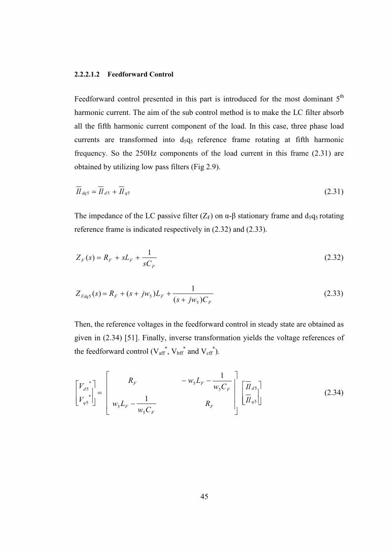
45
2.2.2.1.2 Feedforward Control
Feedforward control presented in this part is introduced for the most dominant 5th
harmonic current. The aim of the sub control method is to make the LC filter absorb
all the fifth harmonic current component of the load. In this case, three phase load
currents are transformed into d5q5 reference frame rotating at fifth harmonic
frequency. So the 250Hz components of the load current in this frame (2.31) are
obtained by utilizing low pass filters (Fig 2.9).
555 qddq IlIlIl += (2.31)
The impedance of the LC passive filter (ZF) on α-β stationary frame and d5q5 rotating
reference frame is indicated respectively in (2.32) and (2.33).
F
FFFsC
sLRsZ1
)( ++= (2.32)
F
FFFdqCjws
LjwsRsZ)(
1)()(
5
55 ++++= (2.33)
Then, the reference voltages in the feedforward control in steady state are obtained as
given in (2.34) [51]. Finally, inverse transformation yields the voltage references of
the feedforward control (Vaff*, Vbff
* and Vcff*).
−
−−
=
5
5
5
5
5
5
*
5
*
5
1
1
q
d
F
F
F
F
FF
q
d
Il
Il
RCw
Lw
CwLwR
V
V (2.34)
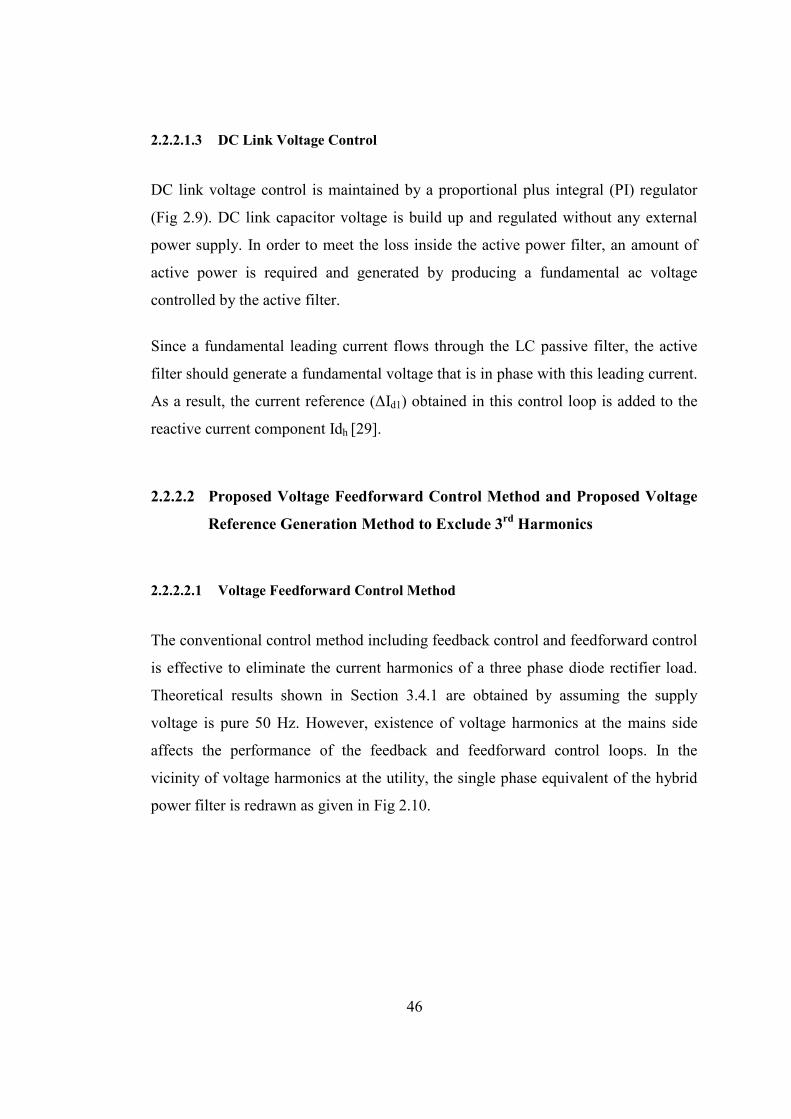
46
2.2.2.1.3 DC Link Voltage Control
DC link voltage control is maintained by a proportional plus integral (PI) regulator
(Fig 2.9). DC link capacitor voltage is build up and regulated without any external
power supply. In order to meet the loss inside the active power filter, an amount of
active power is required and generated by producing a fundamental ac voltage
controlled by the active filter.
Since a fundamental leading current flows through the LC passive filter, the active
filter should generate a fundamental voltage that is in phase with this leading current.
As a result, the current reference (∆Id1) obtained in this control loop is added to the
reactive current component Idh [29].
2.2.2.2 Proposed Voltage Feedforward Control Method and Proposed Voltage
Reference Generation Method to Exclude 3rd Harmonics
2.2.2.2.1 Voltage Feedforward Control Method
The conventional control method including feedback control and feedforward control
is effective to eliminate the current harmonics of a three phase diode rectifier load.
Theoretical results shown in Section 3.4.1 are obtained by assuming the supply
voltage is pure 50 Hz. However, existence of voltage harmonics at the mains side
affects the performance of the feedback and feedforward control loops. In the
vicinity of voltage harmonics at the utility, the single phase equivalent of the hybrid
power filter is redrawn as given in Fig 2.10.

47
Ish
IlhVsh
Zf
+
-Vff β
Zs
α2α1
K
Ifh
Fig 2.10 Single Phase Equivalent of Hybrid Power Filter (Supply Side Voltage Harmonics are existing)
In previous single phase analysis, utility voltage is assumed to be pure 50 Hz. In this
case a voltage harmonic component (Vsh) is introduced with zero phase angle. The
harmonic components of the source current can be represented as given in (2.35)
)( 21 α
α∠×
+++
++∠
= lh
sf
f
sf
shsh I
ZZK
Z
ZZK
VI (2.35)
Assume no feedback control is applied (K=0);
)( 21 α
α∠×
++
+∠
= lh
sf
f
sf
ssh I
ZZ
Z
ZZ
VI (2.36)
Iadd Iprev
It is shown in (2.36) that, Iadd is the additional harmonic current flow at the source
side due to the existence of utility voltage harmonic. The resultant effect between
these two current vectors (Iadd, Iprev) can be either additive or subtractive which is
determined by the their phase angles (α1, α2). In order to diminish this additional
current flow, a voltage term (Vff) should be generated at the output of the active
power filter (2.37).

48
)( 2
1 αβα
∠×+
++
∠−∠= lh
sf
f
sf
ffsh
sh IZZ
Z
ZZ
VVI (2.37)
If the generated voltage term is equal to the existing voltage harmonics in both
magnitude and phase (Vff = Vsh, β = α1), additional current flow is prevented. As a
result, the voltage feedforward control method given in Fig 2.11 is proposed. It
mainly depends on extracting the supply voltage harmonic component and isolating
the hybrid power filter from any harmonic current flow [52].
Since the 5th voltage harmonic is the most probable component that may appear on
the utility, the block diagram of the control method (Fig 2.11) is given to isolate 5th
voltage harmonic. Similar to feedback control method, synchronous reference frame
method is utilized. Three phase utility voltages, which are already sampled for PLL
(Section 2.2.2.1.1), are also transformed into d5-q5 reference frame which is rotating
with an angular frequency of w5 (5w1). The angle used in the Park transformation
(w5) can be easily obtained by a simple multiplication and mod operation of the PLL
output (w1). After applying the park transformation, 250 Hz components of the utility
voltage which are DC quantities with respect to d5-q5 reference frame, are obtained
by employing LPFs.
Fig 2.11 Proposed Voltage Feedforward Control Method

49
Finally, similar to feedback control, the voltage references of the proposed control
method (Vaff2*, Vbff2
*, Vcff2*) are obtained by utilizing Inverse Park and Inverse
Clarke Transformations respectively. Obtained voltage references should be added
with the voltage references obtained in Section 2.2.2.1.1 and 2.2.2.1.2. The
interaction between the existing voltage harmonics at the mains side and the current
harmonics of the load is given by simulation results in Section 3.4.2.
2.2.2.2.2 Proposed Voltage Reference Generation Method to Exclude 3rd Harmonics
The performance of the conventional control method applied for the transformerless
hybrid power filter is quite satisfactory as given in Section 3.4.1. However, if the
harmonic content of the non-linear load includes unbalanced 3rd harmonic
components, it is not possible to compensate these components without a neutral
conductor. Therefore, 3rd harmonic should be excluded during the current reference
calculations. However, in the conventional control method, 50 Hz component of the
source current is extracted and the remaining part is treated as the harmonic current
reference of the system. In the proposed control method, the harmonic content of the
load is calculated for each dominant harmonic frequency by using synchronous
reference frame method.
The load current (IL) and the hybrid power filter current (IF) can be represented in α-
β stationary reference frame as follows:
+++
+++
=
=
∑
∑
=
=
))cos()cos((
))sin()sin((
),(
2111
2111
kk
n
k
kLL
kk
n
k
kLL
L
L
L
twItwI
twItwI
I
II
λλ
λλβα
ββ
αα
β
α (2.38)
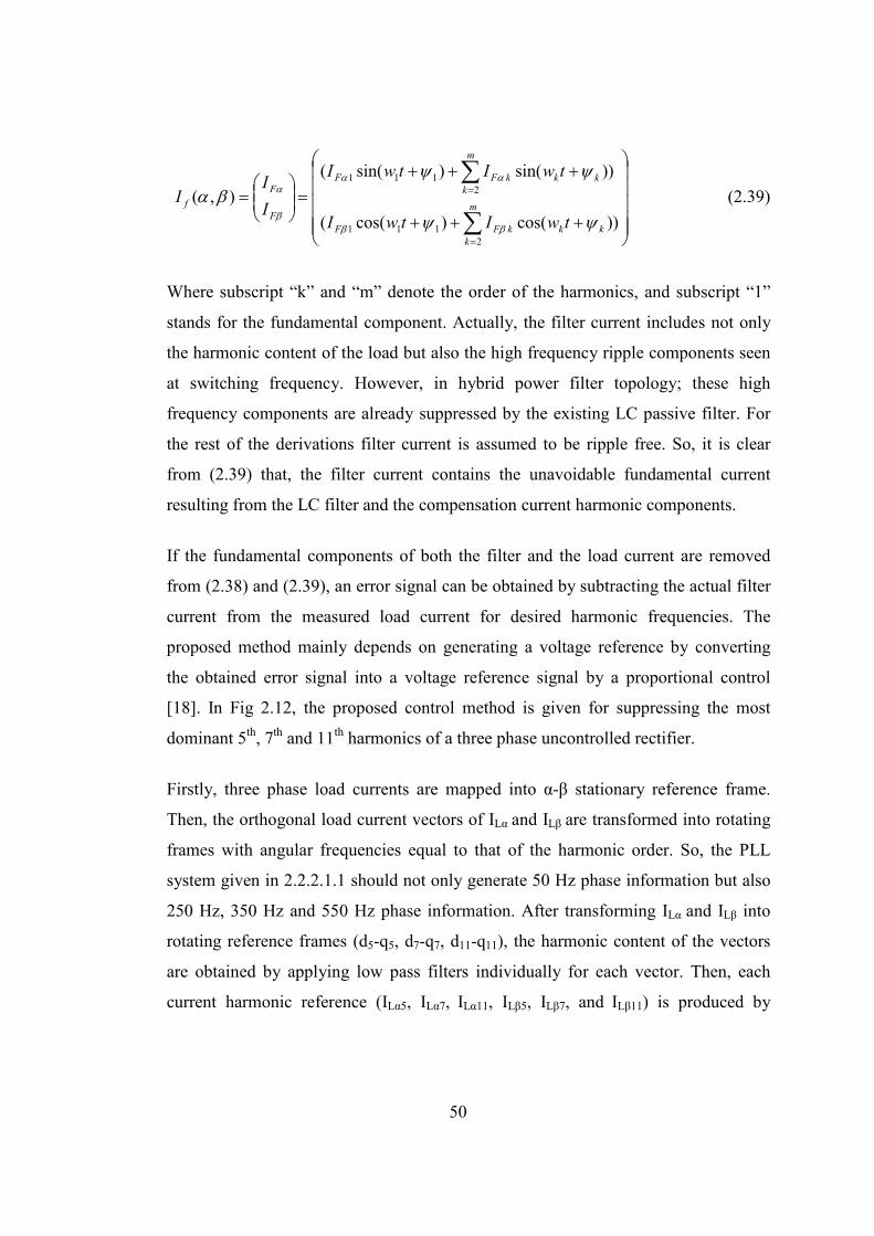
50
+++
+++
=
=
∑
∑
=
=
))cos()cos((
))sin()sin((
),(
2111
2111
kk
m
k
kFF
kk
m
k
kFF
F
F
f
twItwI
twItwI
I
II
ψψ
ψψβα
ββ
αα
β
α (2.39)
Where subscript “k” and “m” denote the order of the harmonics, and subscript “1”
stands for the fundamental component. Actually, the filter current includes not only
the harmonic content of the load but also the high frequency ripple components seen
at switching frequency. However, in hybrid power filter topology; these high
frequency components are already suppressed by the existing LC passive filter. For
the rest of the derivations filter current is assumed to be ripple free. So, it is clear
from (2.39) that, the filter current contains the unavoidable fundamental current
resulting from the LC filter and the compensation current harmonic components.
If the fundamental components of both the filter and the load current are removed
from (2.38) and (2.39), an error signal can be obtained by subtracting the actual filter
current from the measured load current for desired harmonic frequencies. The
proposed method mainly depends on generating a voltage reference by converting
the obtained error signal into a voltage reference signal by a proportional control
[18]. In Fig 2.12, the proposed control method is given for suppressing the most
dominant 5th, 7th and 11th harmonics of a three phase uncontrolled rectifier.
Firstly, three phase load currents are mapped into α-β stationary reference frame.
Then, the orthogonal load current vectors of ILα and ILβ are transformed into rotating
frames with angular frequencies equal to that of the harmonic order. So, the PLL
system given in 2.2.2.1.1 should not only generate 50 Hz phase information but also
250 Hz, 350 Hz and 550 Hz phase information. After transforming ILα and ILβ into
rotating reference frames (d5-q5, d7-q7, d11-q11), the harmonic content of the vectors
are obtained by applying low pass filters individually for each vector. Then, each
current harmonic reference (ILα5, ILα7, ILα11, ILβ5, ILβ7, and ILβ11) is produced by

51
applying inverse park transformation. Thus, (2.38) can be modified to produce the
current harmonic references as indicated in (2.40).
+++++
+++++=
)cos()cos()cos(
)sin()sin()sin(
777777555
777777555
*
*
λλλ
λλλ
βββ
ααα
β
α
twItwItwI
twItwItwI
I
I
LLL
LLL
L
L (2.40)
After transforming the hybrid power filter current into the same reference frame, the
error signal is obtained by subtracting it from the reference current vectors (ILα*,
ILβ*). Even though the compensating current references only include harmonics, the
error signal still contains the 50 Hz component of the filter current. Hence, the
unavoidable 50 Hz component is eliminated from the error signal by applying
another Park Transformation and HPF operation respectively. As a result, the error
signal (errordh, errorqh) which contains only the oscillating harmonic components are
obtained.
Similar to feedback control described in Section 2.2.2.1.1, DC link voltage control is
obtained by a proportional plus integral (PI) regulator. The output reference of the PI
controller (∆Id1) should be added to the reactive current component to generate a
fundamental voltage in phase with the leading current of the passive filter. However,
it is not applicable to add “∆Id1” to “errordh” on the rotating reference frame.
Finally, the error signals “errordh and errorqh”, obtained in d-q reference frame, are
transformed into α-β reference frame and amplified with a proportional constant of
“K” to obtain a compensating voltage reference. The compensating voltage and the
DC link references are eventually added and transformed into stationary abc
reference frame (Va*, Vb
*, Vc*) which are modulated to obtain the gate pulses of the
semiconductor switches.
The proposed method assures removing the 150Hz components from the
compensation references of the hybrid power filter and given for 5th, 7th and 11th
harmonics (Fig 2.12). It is clear that, obtaining the current harmonic references in α-β

52
reference frame for each harmonic frequency increases the computation load of the
control system. In the digital implementation of the proposed method, 40us sampling
time is sufficient to perform all these calculations. However, if the number of the
dominant harmonics to be compensated increase, the indicated sampling time may be
insufficient thus decreases the system performance. It can be concluded that, the
proposed voltage reference generation method is applicable to eliminate few critical
harmonics of the load.

53
Fig 2.12 Proposed Voltage Reference Generation Method to Exclude 3rd Harmonics
53
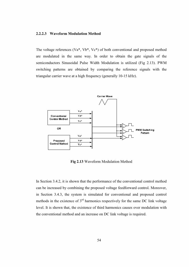
54
2.2.2.3 Waveform Modulation Method
The voltage references (Va*, Vb*, Vc*) of both conventional and proposed method
are modulated in the same way. In order to obtain the gate signals of the
semiconductors Sinusoidal Pulse Width Modulation is utilized (Fig 2.13). PWM
switching patterns are obtained by comparing the reference signals with the
triangular carrier wave at a high frequency (generally 10-15 kHz).
Fig 2.13 Waveform Modulation Method
In Section 3.4.2, it is shown that the performance of the conventional control method
can be increased by combining the proposed voltage feedforward control. Moreover,
in Section 3.4.3, the system is simulated for conventional and proposed control
methods in the existence of 3rd harmonics respectively for the same DC link voltage
level. It is shown that, the existence of third harmonics causes over modulation with
the conventional method and an increase on DC link voltage is required.
55
CHAPTER 3
3 CIRCUIT DESIGN FOR HYBRID POWER FILTER
PROTOTYPE
3.1 Harmonic Content of the Load Obtained by Measurement
Results
In TÜBĐTAK Space Technologies Institute, presence of diode rectifier loads
(including especially the personal computer loads) results in distorted current at
400V low voltage side. In order to determine the capacity of the hybrid power filter,
measurements are performed as a preliminary design work. In this Section, the
measurement results are given to show the amount of distortion at supply current.
Three phase current and voltage raw data are stored during 6 hours period with a
sampling rate of 6400 sample/sec. The raw data are processed with 10 cycle
resolution and values are restored as 3 second averages as indicated in the harmonic
standard [8]. Distorted line current waveforms for each phase are given in Fig 3.1,
Fig 3.2 and Fig 3.3 respectively. In order to show the amount of the distortion in the
current, harmonic components are represented in terms of maximum demand load
current (IL). As described in Section 1.1, maximum demand load current is calculated
by the average of the last twelve monthly peak demand. However, since the
measurement duration is 6 hours, peak demand is taken as the maximum of the
fundamental current component of 15 minutes averages (Fig 3.4, Fig 3.5). Odd
harmonics of each phase are shown in terms of both magnitude and percent of IL (Fig
3.6 to Fig 3.14). Limit value defined in IEEE 519 standards is drawn with a red line
for each harmonic component.

56
0 10 20 30 40 50 60 70 80 90 100-400
-300
-200
-100
0
100
200
300
400
Time (msec)
Magnitude (V & A)
Line Current & Voltage (Phase A)
Current
Voltage
6400 sample/sec
Fig 3.1 Line Current and Voltage (Phase A)
0 10 20 30 40 50 60 70 80 90 100-400
-300
-200
-100
0
100
200
300
400
Time (msec)
Magnitude (V & A)
Line Current & Voltage (Phase B)
Current
Voltage
6400 sample/sec
Fig 3.2 Line Current and Voltage (Phase B)

57
0 10 20 30 40 50 60 70 80 90 100-400
-300
-200
-100
0
100
200
300
400
Time (msec)
Magnitude (V & A)
Line Current & Voltage (Phase C)
Current
Voltage
6400 sample/sec
Fig 3.3 Line Current and Voltage (Phase C)
0 30 60 90 120 150 180 210 240 270 300 330 3600
50
100
150
200
250
300
350
Time (minute)
Magnitude (A RMS)
Line Current Fundamental Component
Phase A
Phase B
Phase C
6400 sample/sec
Fig 3.4 Fundamental Component of Line Current (3 sec. average, Field Data)

58
0 50 100 150 200 250 300 3500
50
100
150
200
250
300
Time (minute)
Magnitude (A RMS)
Line Current Fundamental Component
Phase A
Phase B
Phase C
6400 sample/sec
Fig 3.5 Fundamental Component of Line Current (15 min. average, Field Data)
0
2.3663
4.7326
7.0989
9.4653
11.8316
14.1979
16.5642
0
2.3663
4.7326
7.0989
9.4653
11.8316
14.1979
16.5642
0
2.3663
4.7326
7.0989
9.4653
11.8316
14.1979
16.5642
0
2.3663
4.7326
7.0989
9.4653
11.8316
14.1979
16.5642
3rd Harmonic Component (A RMS)
0 30 60 90 120 150 180 210 240 270 300 330 3600
1
2
3
4
5
6
7
3rd Harmonic Component (%IL)
Time (minute)
Line Current 3rd Harmonic
Phase A
Phase B
Phase C
Limit
PENALTY LIMIT 6400 sample/sec
Fig 3.6 3rd Harmonic Component of Line Current (3 sec. average, Field Data)

59
0
4.7326
9.4653
14.1979
18.9305
23.6632
0
4.7326
9.4653
14.1979
18.9305
23.6632
0
4.7326
9.4653
14.1979
18.9305
23.6632
0
4.7326
9.4653
14.1979
18.9305
23.6632
5th Harmonic Component (A RMS)
0 30 60 90 120 150 180 210 240 270 300 330 3600
2
4
6
8
105th Harmonic Component (%IL)
Time (minute)
Line Current 5th Harmonic
Phase A
Phase B
Phase C
Limit
PENALTY LIMIT
6400 sample/sec
Fig 3.7 5th Harmonic Component of Line Current (3 sec. average, Field Data)
0
1.1832
2.3663
3.5495
4.7326
5.9158
7.0989
8.2821
9.4653
10.6484
11.8316
0
1.1832
2.3663
3.5495
4.7326
5.9158
7.0989
8.2821
9.4653
10.6484
11.8316
0
1.1832
2.3663
3.5495
4.7326
5.9158
7.0989
8.2821
9.4653
10.6484
11.8316
0
1.1832
2.3663
3.5495
4.7326
5.9158
7.0989
8.2821
9.4653
10.6484
11.8316
7th Harmonic Component (A RMS)
0 30 60 90 120 150 180 210 240 270 300 330 3600
0.5
1
1.5
2
2.5
3
3.5
4
4.5
5
7th Harmonic Component (%IL)
Time (minute)
Line Current 7th Harmonic
Phase A
Phase B
Phase C
Limit
PENALTY LIMIT
6400 sample/sec
Fig 3.8 7th Harmonic Component of Line Current (3 sec. average, Field Data)

60
0
1.1832
2.3663
3.5495
4.7326
5.9158
7.0989
8.2821
9.4653
0
1.1832
2.3663
3.5495
4.7326
5.9158
7.0989
8.2821
9.4653
0
1.1832
2.3663
3.5495
4.7326
5.9158
7.0989
8.2821
9.4653
0
1.1832
2.3663
3.5495
4.7326
5.9158
7.0989
8.2821
9.4653
9th Harmonic Component (A RMS)
0 30 60 90 120 150 180 210 240 270 300 330 3600
0.5
1
1.5
2
2.5
3
3.5
4
9th Harmonic Component (%IL)
Time (minute)
Line Current 9th Harmonic
Phase A
Phase B
Phase C
Limit
6400 sample/sec
PENALTY LIMIT
Fig 3.9 9th Harmonic Component of Line Current (3 sec. average, Field Data)
0
1.1832
2.3663
3.5495
4.7326
5.9158
0
1.1832
2.3663
3.5495
4.7326
5.9158
0
1.1832
2.3663
3.5495
4.7326
5.9158
0
1.1832
2.3663
3.5495
4.7326
5.9158
11th Harmonic Component (A RMS)
0 30 60 90 120 150 180 210 240 270 300 330 3600
0.5
1
1.5
2
2.5
11th Harmonic Component (%IL)
Time (minute)
Line Current 11th Harmonic
Phase A
Phase B
Phase C
Limit
PENALTY LIMIT
6400 sample/sec
Fig 3.10 11th Harmonic Component of Line Current (3 sec. average, Field Data)
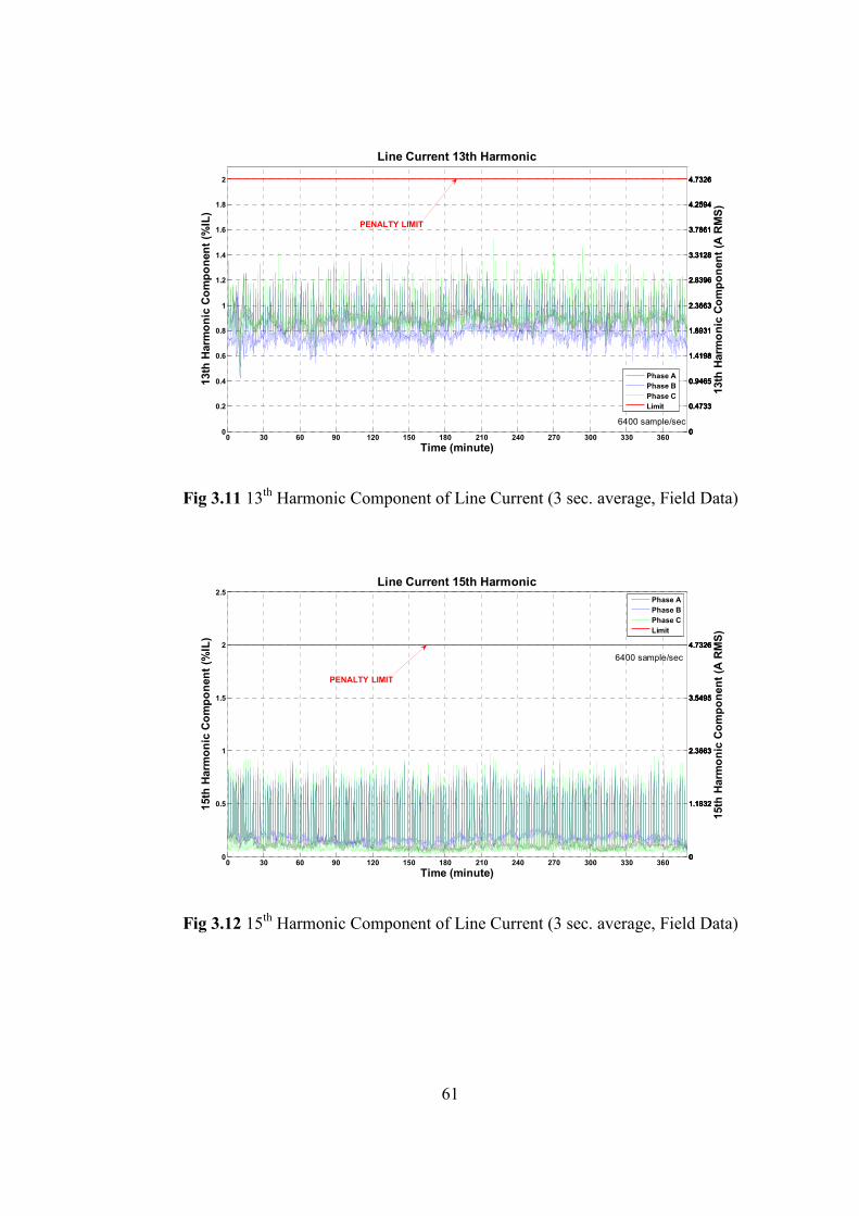
61
0
0.4733
0.9465
1.4198
1.8931
2.3663
2.8396
3.3128
3.7861
4.2594
4.7326
0
0.4733
0.9465
1.4198
1.8931
2.3663
2.8396
3.3128
3.7861
4.2594
4.7326
0
0.4733
0.9465
1.4198
1.8931
2.3663
2.8396
3.3128
3.7861
4.2594
4.7326
0
0.4733
0.9465
1.4198
1.8931
2.3663
2.8396
3.3128
3.7861
4.2594
4.7326
13th Harmonic Component (A RMS)
0 30 60 90 120 150 180 210 240 270 300 330 3600
0.2
0.4
0.6
0.8
1
1.2
1.4
1.6
1.8
2
13th Harmonic Component (%IL)
Time (minute)
Line Current 13th Harmonic
Phase A
Phase B
Phase C
Limit
PENALTY LIMIT
6400 sample/sec
Fig 3.11 13th Harmonic Component of Line Current (3 sec. average, Field Data)
0
1.1832
2.3663
3.5495
4.7326
0
1.1832
2.3663
3.5495
4.7326
0
1.1832
2.3663
3.5495
4.7326
0
1.1832
2.3663
3.5495
4.7326
15th Harmonic Component (A RMS)
0 30 60 90 120 150 180 210 240 270 300 330 3600
0.5
1
1.5
2
2.5
15th Harmonic Component (%IL)
Time (minute)
Line Current 15th Harmonic
Phase A
Phase B
Phase C
Limit
PENALTY LIMIT
6400 sample/sec
Fig 3.12 15th Harmonic Component of Line Current (3 sec. average, Field Data)

62
0
0.4733
0.9465
1.4198
1.8931
2.3663
2.8396
3.3128
3.7861
0
0.4733
0.9465
1.4198
1.8931
2.3663
2.8396
3.3128
3.7861
0
0.4733
0.9465
1.4198
1.8931
2.3663
2.8396
3.3128
3.7861
0
0.4733
0.9465
1.4198
1.8931
2.3663
2.8396
3.3128
3.7861
17th Harmonic Component (A RMS)
0 30 60 90 120 150 180 210 240 270 300 330 3600
0.2
0.4
0.6
0.8
1
1.2
1.4
1.6
17th Harmonic Component (%IL)
Time (minute)
Line Current 17th Harmonic
Phase A
Phase B
Phase C
Limit
PENALTY LIMIT
6400 sample/sec
Fig 3.13 17th Harmonic Component of Line Current (3 sec. average, Field Data)
0
0.4733
0.9465
1.4198
1.8931
2.3663
2.8396
3.3128
3.7861
0
0.4733
0.9465
1.4198
1.8931
2.3663
2.8396
3.3128
3.7861
0
0.4733
0.9465
1.4198
1.8931
2.3663
2.8396
3.3128
3.7861
0
0.4733
0.9465
1.4198
1.8931
2.3663
2.8396
3.3128
3.7861
19th Harmonic Component (A RMS)
0 30 60 90 120 150 180 210 240 270 300 330 3600
0.2
0.4
0.6
0.8
1
1.2
1.4
1.6
19th Harmonic Component (%IL)
Time (minute)
Line Current 19th Harmonic
Phase A
Phase B
Phase C
Limit
6400 sample/sec
PENALTY LIMIT
Fig 3.14 19th Harmonic Component of Line Current (3 sec. average, Field Data)
63
Measurement results have shown that, at TÜBĐTAK Space Technologies Institute’s
400V bus, 5th, 7th and 11th harmonic components are the most dominant harmonics
which are above the limits as expected. In Section 3.2.1, the measurement results are
utilized in order to model the non-linear load and the system.
3.2 Simulation Model of the System
In this thesis work, simulation model of the system is formed by using
EMTDC/PSCAD 4.2.0 Professional software. The transformerless hybrid power
filter system is modeled, simulated and analyzed in PSCAD 4.2.0 environment [53].
Moreover, AC analysis of the passive filter is performed by using Ansoft Simplorer
7.0 software [54].
In order to achieve compatibility with the experimental system, instead of using the
available mathematical blocks of PSCAD, the control methods described in Section
2.2.2 are developed in FORTRAN language. Moreover, theoretical results obtained
by simulations are evaluated and shown by using MATLAB 6.5 [55].
3.2.1 Load Modeling
The measurement results represented in Section 3.1 indicates that, 5th, 7th and 11th
harmonics are the most dominant current harmonics existing at TÜBĐTAK Space
Technologies Institute. The magnitude of the most dominant harmonics is nearly 30
ARMS. By considering the possibility of new computer loads in future, VSC based
Hybrid Active Power Filter is designed to have a 50 ARMS harmonic current filtering
capacity.

64
I filter
Lf
Cf
Rf
S1
S2
S3
S4
S5
S6
Fig 3.15 Simulation Model of the Transformerless Shunt Hybrid Power Filter In Fig 3.15, three phase representation of the Hybrid power filter and the non-linear
load is represented. In addition to 5th, 7th and 11th harmonics, 3rd harmonics are also
observed (Fig 3.6) at the source side due to the fluorescent lamp loads. So, in the
non-linear load model, single phase rectifiers with RL load are also used to introduce
3rd harmonic.
The existing system includes a 34.5/0.4kV delta-wye transformer at the AC line. In
simulation work, it is modeled as an AC voltage source (400Vline, 50Hz) in series
with the transformer’s leakage reactance. The parameters Ls and Rs are calculated as
given below:

65
S=1.25MVA (VA rating of the transformer)
Uk = 6%
So, the 400V secondary side of the transformer is referred as follows;
uH25502
1U
S
VL k
2
s ≅π
××= (3.1)
Ω≅×π
= m77.0L10
502R ss (3.2)
Table 3.1 System Parameters
Line Voltage 400 V-rms
Line frequency 50 Hz
Supply inductance (Ls) 25 uH
Filter Capacitor (Cf) 0.6 mF
Filter Inductance (Lf) 365 uH
Tuned freq. of series filter 340 Hz
DC link capacitor (Cdc) 7 mF
Load Inductances(Lac1, Lac2, Lac3, Lac4) 0.5mH, 2.5mH, 1.5mH, 2.5mH
Load Inductances(Lload1, Lload2, Lload3, Lload4) 2mH, 3mH, 3.5mH, 3mH
Load Resistances(Rload1, Rload2, Rload3, Rload4) 3Ω, 2Ω, 1.5Ω, 1.8Ω
Load Capacitor (Cload) 2mF
When the system is simulated under the non-linear load condition given in Fig 3.15
and Table 3.1, the harmonic spectrum of the load current which is similar to
measurement results is shown in Table 3.2. The distorted current waveform of the
source current and mains voltage are shown in Fig 3.16 and Fig 3.17 respectively.

66
Table 3.2 Harmonic Spectrum of Actual Load and Simulation Load Model
ARMS Fund. 3rd 5th 7th 11th 13th 17th 19th
Measurement Results 200-250.0 ~9.5 ~23.0 ~11.0 ~4.7 ~2.0 ~1.4 ~1.4
Simulation Load Model 225-247.0 ~10.7 ~23.6 ~12.5 ~4.86 ~3.24 ~1.9 ~1.4
Fig 3.16 Mains Voltage and Load Current

67
Fig 3.17 Load Current
3.3 Design of Circuit Elements
3.3.1 Passive Filter Capacitor and Reactor
The series connected capacitor (CF) and the filter reactor (LF) forms a LC passive
filter. So that, the LC filters should be chosen to eliminate the most dominant 5th or
7th harmonic of the diode rectifier load. Although the 5th harmonic component of the
non-linear load is the most dominant component, it is reasonable to tune the LC filter
at seventh harmonic frequency. The passive filter tuned to 350 Hz shows lower
impedance at 550 Hz and 650 Hz than a passive filter tuned to 250 Hz. Moreover, the
passive filter tuned to 7th harmonic frequency is less bulky than a 5th harmonic filter
for the same filter capacitor (CF) [56].
The characteristic impedance of the passive filter (Z) is defined as given in (3.3). The
filtering performance of the passive filter is determined by this impedance except for
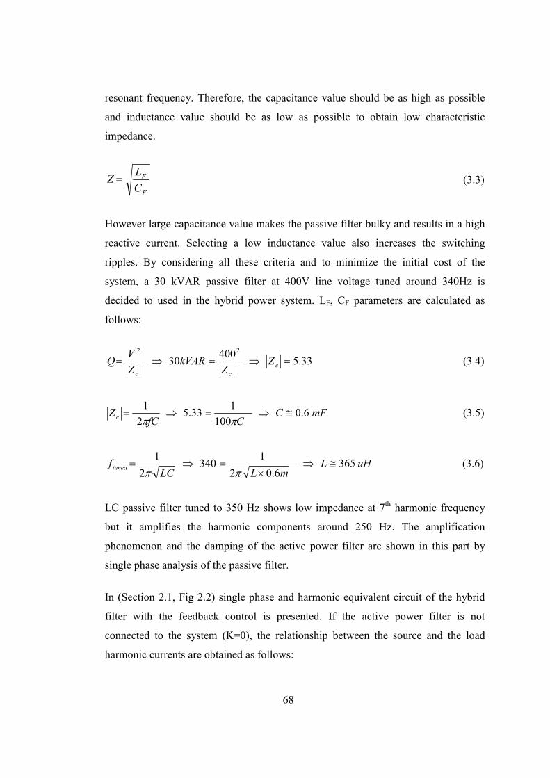
68
resonant frequency. Therefore, the capacitance value should be as high as possible
and inductance value should be as low as possible to obtain low characteristic
impedance.
F
F
C
LZ = (3.3)
However large capacitance value makes the passive filter bulky and results in a high
reactive current. Selecting a low inductance value also increases the switching
ripples. By considering all these criteria and to minimize the initial cost of the
system, a 30 kVAR passive filter at 400V line voltage tuned around 340Hz is
decided to used in the hybrid power system. LF, CF parameters are calculated as
follows:
33.5400
3022
=⇒=⇒= c
cc
ZZ
kVARZ
VQ (3.4)
mFCCfC
Z c 6.0100
133.5
2
1≅⇒=⇒=
ππ (3.5)
uHLmLLC
f tuned 3656.02
1340
2
1≅⇒
×=⇒=
ππ (3.6)
LC passive filter tuned to 350 Hz shows low impedance at 7th harmonic frequency
but it amplifies the harmonic components around 250 Hz. The amplification
phenomenon and the damping of the active power filter are shown in this part by
single phase analysis of the passive filter.
In (Section 2.1, Fig 2.2) single phase and harmonic equivalent circuit of the hybrid
filter with the feedback control is presented. If the active power filter is not
connected to the system (K=0), the relationship between the source and the load
harmonic currents are obtained as follows:

69
shfh
fh
shZZ
ZI
+= (3.7)
By using the single phase equivalent circuit given in Section 2.1, the load is modeled
as an ideal current source. AC analysis results of the passive filter specified above
shows that, the current components between 230 Hz and 320 are amplified when
only the passive filter is connected to the system (Fig 3.18). However, when active
power filter is joined with the feedback control, the feedback gain K acts as a
damping resistor which suppresses the resonance between the supply and the passive
filter. As shown in Fig 3.19, if the feedback gain is increased, the harmonic content
of the source current decreases significantly. However, feedback gain is limited to
certain values in order to avoid stability problems in the control loop of the active
power filter.
0 100 200 300 400 500 600 700 800 900 100010
-1
100
101
Mains Current Frequency Spectrum
Frequency (Hz)
Amplitude (A)
K=0
Fig 3.18 Mains Current Frequency Spectrum (Passive Filter)
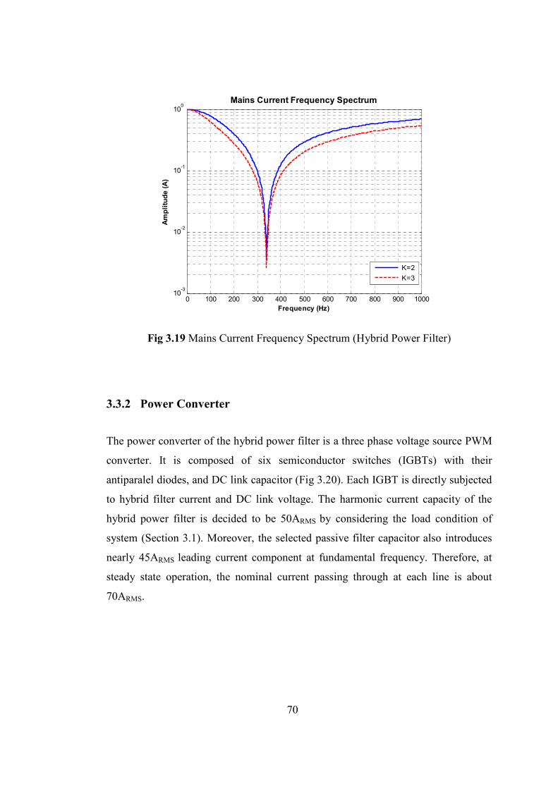
70
0 100 200 300 400 500 600 700 800 900 100010
-3
10-2
10-1
100
Mains Current Frequency Spectrum
Frequency (Hz)
Amplitude (A)
K=2
K=3
Fig 3.19 Mains Current Frequency Spectrum (Hybrid Power Filter)
3.3.2 Power Converter
The power converter of the hybrid power filter is a three phase voltage source PWM
converter. It is composed of six semiconductor switches (IGBTs) with their
antiparalel diodes, and DC link capacitor (Fig 3.20). Each IGBT is directly subjected
to hybrid filter current and DC link voltage. The harmonic current capacity of the
hybrid power filter is decided to be 50ARMS by considering the load condition of
system (Section 3.1). Moreover, the selected passive filter capacitor also introduces
nearly 45ARMS leading current component at fundamental frequency. Therefore, at
steady state operation, the nominal current passing through at each line is about
70ARMS.

71
Fig 3.20 Voltage Source Converter However, the DC link voltage is not as crucial as the current specification of the
semiconductor device because the DC link voltage is quite below when compared
with a pure shunt connected active power filter [52, 57]. 250V to 6.6kV IGBT
modules are commercially available on the market. However, for a low rated
converter topology, it is not reasonable to form the inverter with single IGBT
packages due to the design complexity of the busbar and higher cost. Therefore, 6-
pack intelligent power modules (IPM) with their high speed, low loss and optimized
gate drives are seem to be an appropriate solution for this application.
3.3.3 DC Link
In conventional pure shunt connected voltage source active power filters, DC link
voltage is required to be higher than the peak value of the utility voltage; otherwise,
the generated compensation currents cannot be injected to the mains [57]. However,
transformerless hybrid power filter provides a reduced DC link voltage.
So, the DC link voltage is kept as low as possible while observing the filtering
performance of the system. The optimum DC link voltage is found by means of

72
simulation as shown in Section 3.4.1, 3.4.2 and 3.4.3. The selection of the DC link
capacitor is also based on simulation analysis to minimize the voltage ripple. As can
be seen from theoretical results, 7mF DC link capacitor is complying with the
minimum voltage ripple criteria of the DC link voltage. However, ripple current
rating, power loss, temperature rise of the capacitor and the life time of the
component should also be analyzed for the experimental set up. In Section 4.1.2, the
design guide is also provided for the experimentally utilized DC link capacitor.
3.4 Theoretical Results
Theoretical results are obtained for the system given in Fig 3.15, using PSCAD
software in a way to minimize the DC link voltage and the rating of the APF, while
keeping the filtering performance satisfactory. In this part of the thesis, firstly the
theoretical results obtained with the conventional control method are represented.
Then, the proposed control methods are investigated. The startup procedure of the
system for both control methods is as follows:
• Initially, three upper IGBTs (S1, S2, S3) are turned ON and three lower
IGBTs (S4, S5, S6) are turned OFF. During this time interval, active filter is
not operating, and DC side of the active filter is seen as a short circuit by the
mains side.
• When circuit breaker (BRK1) is closed, the system operates only as a passive
LC filter
• After DC link voltage is built up to the specified reference value, the
compensation current references are activated in the control loop of the
system and hybrid power filter totally operates.
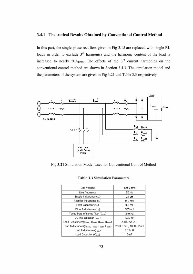
73
3.4.1 Theoretical Results Obtained by Conventional Control Method
In this part, the single phase rectifiers given in Fig 3.15 are replaced with single RL
loads in order to exclude 3rd harmonics and the harmonic content of the load is
increased to nearly 50ARMS. The effects of the 3rd current harmonics on the
conventional control method are shown in Section 3.4.3. The simulation model and
the parameters of the system are given in Fig 3.21 and Table 3.3 respectively.
Fig 3.21 Simulation Model Used for Conventional Control Method
Table 3.3 Simulation Parameters
Line Voltage 400 V-rms
Line frequency 50 Hz
Supply inductance (Ls) 25 uH
Rectifier inductance (Ll) 0.1 mH
Filter Capacitor (CF) 0.6 mF
Filter Inductance (LF) 365 uH
Tuned freq. of series filter (ftuned) 340 Hz
DC link capacitor (CDC) 7.05 mF
Load Resistances(Rload1, Rload2, Rload3, Rload4) 2.1Ω, 2Ω, 2 Ω
Load Inductances(Lload1, Lload2, Lload3, Lload4) 2mH, 10uH, 10uH, 10uH
Load Inductances(Lac1) 0.15mH
Load Capacitor (Cload) 2mF

74
“Table 3.3 Cont’d”
Switching frequency (fswitching) 10kHz
Simulation Step Time 10usec
Feedback Gain (K) 2
Harmonic content of the supply current is obtained by Synchronous Reference Frame
method as described previously. The phase information of the supply voltage is
obtained by a PLL system, as given in Section 2.2.2.1.1. As can be seen from Fig
3.22, the phase angle information (w1t) is locked to the supply voltage between 0-2π
which is utilized in the transformation matrices.
Fig 3.22 Phase Locked Loop (PLL) Output at Steady State
In Fig 3.23 and Fig 3.24 simulation results obtained during the start up procedure are
shown. At t=80 ms, circuit breaker (BRK1) is turned on and 7th tuned LC passive
filter starts to operate. The performance of the filter is similar to the results of the
single phase analysis with zero feedback gain described in Section 3.3.1 (Fig 3.18).
After several cycles (t=300 ms), the voltage reference (∆Id1) required to built up the
DC link voltage to 120V is activated. Filter current and DC link voltage response
during this interval is represented in Fig 3.24.

75
Fig 3.23 During Start Up, Mains Voltage (200V/div), Load Current (250A/div), Source Current (250A/div), Filter Current (100A/div)
Fig 3.24 DC Link Voltage Built Up, DC Link Voltage (50V/div), Filter Current (50A/div)

76
When DC link capacitor voltage is set to 120V, the voltage references (Vafb*, Vbfb
*,
Vcfb*) obtained in the feedback control loop are activated (Fig 3.25). The mains
current becomes a sinusoidal waveform, DC link voltage is kept constant at 120V
and filter current is ripple free (Fig 3.26, Fig 3.27). The filtering performance of the
system is as expected with the single phase analysis obtained in Section 3.3.1 (Fig
3.19). The hybrid power filter damps the resonance and the amplification
phenomenon at fifth harmonic frequency disappears.
Fig 3.25 DC Link Voltage (50V/div), Filter Current (100A/div)

77
Fig 3.26 Hybrid Power Filter Steady State Results with Feedback Control
Mains Voltage (200V/div), Load Current (250A/div), Source Current (250A/div), Filter Current (200A/div)
Fig 3.27 Hybrid Power Filter Steady State Results with Feedback Control
DC Link Voltage (50V/div), Load Current (250A/div), Source Current (250A/div), Filter Current (200A/div)

78
Fig 3.28 Hybrid Power Filter Steady State Results with Feedback and
Feedforward Control, Mains Voltage (200V/div), Load Current (250A/div), Source Current (250A/div), Filter Current (200A/div)
Fig 3.29 Hybrid Power Filter Steady State Results with Feedback and
Feedforward Control, DC Link Voltage (50V/div), Load Current (250A/div), Source Current (250A/div), Filter Current (200A/div)
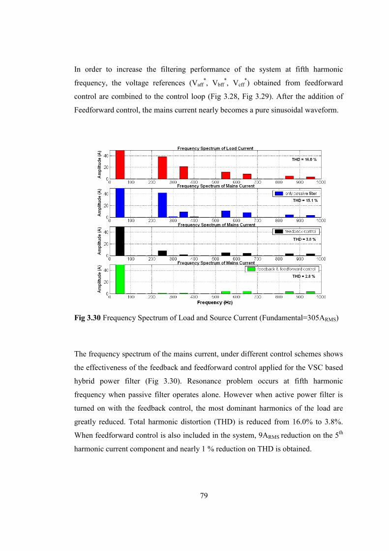
79
In order to increase the filtering performance of the system at fifth harmonic
frequency, the voltage references (Vaff*, Vbff
*, Vcff*) obtained from feedforward
control are combined to the control loop (Fig 3.28, Fig 3.29). After the addition of
Feedforward control, the mains current nearly becomes a pure sinusoidal waveform.
Fig 3.30 Frequency Spectrum of Load and Source Current (Fundamental=305ARMS) The frequency spectrum of the mains current, under different control schemes shows
the effectiveness of the feedback and feedforward control applied for the VSC based
hybrid power filter (Fig 3.30). Resonance problem occurs at fifth harmonic
frequency when passive filter operates alone. However when active power filter is
turned on with the feedback control, the most dominant harmonics of the load are
greatly reduced. Total harmonic distortion (THD) is reduced from 16.0% to 3.8%.
When feedforward control is also included in the system, 9ARMS reduction on the 5th
harmonic current component and nearly 1 % reduction on THD is obtained.

80
The series LC filter of the simulated hybrid filter topology results in an additional
fundamental current flow through the inverter. However, the required DC link
voltage is much less when compared with a standard voltage source type APF [56].
In the simulated system, the DC link voltage is kept constant at 120 VDC.
Moreover, in voltage source active power filter applications, an additional switching
filter is required to isolate the mains side from high frequency ripple currents of the
filter current. Although no additional switching filter is used, high frequency current
ripples are also minimized with the applied system. The main disadvantage of the
hybrid power filter is that, the reactive power compensation capability is limited with
capacity of the used passive filter. Thus, installing hybrid power filter to PCC where
reactive power compensation is critical will not be a good solution.
3.4.2 Theoretical Results Obtained by Proposed Voltage Feedforward
Control Method
In this part, the effect of the existing voltage harmonics on the system which is
controlled by the conventional control method (Section 2.2.2.1) is represented. The
simulation parameters used in this part is similar to given in Table 3.3, except for the
addition of voltage harmonics at the mains side. Then, 3% of the line voltage at
250Hz is added as voltage harmonic and the variation on the supply current is
observed. Firstly, the system is simulated under different voltage harmonic
conditions and only the passive filter is turned on. As can be seen from Table 3.4, the
resultant effect between the existing voltage harmonics and current harmonics of the
load can be either additive or subtractive according to the phase angle of the voltage
harmonics.
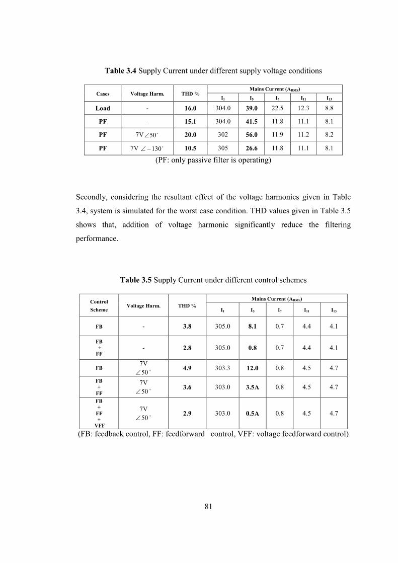
81
Table 3.4 Supply Current under different supply voltage conditions
Cases Voltage Harm. THD % Mains Current (ARMS)
I1 I5 I7 I11 I13
Load - 16.0 304.0 39.0 22.5 12.3 8.8
PF - 15.1 304.0 41.5 11.8 11.1 8.1
PF 7V o50∠ 20.0 302 56.0 11.9 11.2 8.2
PF 7V o130−∠ 10.5 305 26.6 11.8 11.1 8.1
(PF: only passive filter is operating)
Secondly, considering the resultant effect of the voltage harmonics given in Table
3.4, system is simulated for the worst case condition. THD values given in Table 3.5
shows that, addition of voltage harmonic significantly reduce the filtering
performance.
Table 3.5 Supply Current under different control schemes
Control
Scheme Voltage Harm. THD %
Mains Current (ARMS)
I1 I5 I7 I11 I13
FB - 3.8 305.0 8.1 0.7 4.4 4.1
FB + FF
- 2.8 305.0 0.8 0.7 4.4 4.1
FB 7V
o50∠ 4.9 303.3 12.0 0.8 4.5 4.7
FB + FF
7V o50∠
3.6 303.0 3.5A 0.8 4.5 4.7
FB + FF +
VFF
7V o50∠
2.9 303.0 0.5A 0.8 4.5 4.7
(FB: feedback control, FF: feedforward control, VFF: voltage feedforward control)

82
Fig 3.31 Supply Current under Different Control Schemes (FB: Feedback Control, FF: Feedforward Control, VFF: proposed Voltage Feedforward Control)
Moreover, in Fig 3.31, the variation on the source current is represented. Highly
distorted current is transformed into a nearly pure sinusoidal waveform by applying
feedback, feedforward and the proposed voltage feedforward control methods
respectively. It is shown that, when both the conventional feedforward and the
proposed voltage feedforward controls are applied with the feedback control; the
filtering performance is comparable with the non voltage harmonic case (Table 3.5).
3.4.3 Theoretical Results Obtained by Proposed Voltage Reference
Generation Method
Theoretical results in Section 3.4.1 show that the filtering performance of the hybrid
power filter is satisfactory under the three phase diode rectifier load. However, the
actual load also contains unbalanced 3rd harmonic components due to the fluorescent

83
lamp loads (Section 3.1, Fig 3.6). Therefore, in the conventional control method, the
calculated current references [29] also include 3rd harmonic. However, the designed
hybrid active power filter topology is not capable of suppressing these 150Hz
components with a three phase three wire connection. Therefore, a method which
excludes the third harmonic components during the reference current calculation is
proposed in Section 2.2.2.2.2. Moreover, in this part the non-linear load model given
in Fig 3.21 is used to obtain a harmonic content similar to that of the actual load and
the parameters given in Table 3.1 are utilized in this Section.
The harmonic content of the load is lower than the previous load model used in
Section 3.4.1. So that, it is not surprising to obtain a DC link voltage lower than the
previous results obtained in Section 3.4.1. The filtering performance of the hybrid
power filter is analyzed for various DC link voltage levels. It is observed that,
60VDC is the optimum and sufficient voltage level to greatly reduce the harmonic
content of the actual load.
Similar to previous theoretical results, firstly only the passive filter is operated by
closing BRK1. Then the DC link voltage reference and current references are
included in the control method respectively. In Fig 3.32, the rising of DC link voltage
is represented. When the DC link voltage reaches its reference 60V, the PWM
converter is modulated with the error signals obtained in the proposed voltage
reference generation method (Section 2.2.2.2.2, Fig 2.12) while keeping the DC link
voltage constant. Fig 3.33 and Fig 3.34 shows that the after t=800ms, hybrid power
filter is totally operating with the proposed control method. The harmonic content of
the supply current is greatly suppressed for each phase, while keeping the DC link
voltage at very low level (Fig 3.35, Fig 3.36).

84
Fig 3.32 DC Link Voltage Built Up DC Link Voltage (20V/div), Filter Current (50A/div)
Fig 3.33 DC Link Voltage (20V/div), Filter Current (100A/div)

85
Fig 3.34 Hybrid Power Filter Steady State Results with Proposed Control
Mains Voltage (200V/div), Load Current (200A/div), Source Current (200A/div), Filter Current (100A/div)
Fig 3.35 Hybrid Power Filter Steady State Results with Proposed Control
DC Link Voltage (20V/div), Load Current (200A/div), Source Current (200A/div), Filter Current (100A/div)

86
Fig 3.36 Hybrid Power Filter Steady State Results with Proposed Control Source Current Phase A,B,C (200A/div)
Fig 3.37 Frequency Spectrum of Load and Mains Current

87
The effectiveness of the proposed control method can be seen from the frequency
spectrum of load and the mains current given in Fig 3.37. Since the 3rd harmonic is
isolated from the current references, it remains at the same level when the hybrid
filter is operating. However, 5th, 7th, 11th and 13th harmonics are filtered in 85%,
above 90%, 75%, 65% percentages respectively.
In order to show the effects of 3rd harmonics on the conventional control method, the
system is also simulated with the same system parameters and the load configuration
given in Table 3.3 and Fig 3.21. In the proposed control method, it is shown that
60VDC is sufficient to generate the required compensation voltage references.
However, in the conventional method, the generated voltage reference exceeds the
carrier peaks which cause an over modulation. In Fig 3.38, the voltage reference
obtained for unity feedback gain is represented. The source current and the DC link
voltage for unity feedback gain and 60VDC link are also given in Fig 3.40.
Fig 3.38 Carrier Wave and Calculated Voltage Reference

88
Fig 3.39 Carrier Wave and Calculated Voltage Reference
Fig 3.40 Hybrid Power Filter Steady State Results with Conventional Control Method, DC Link Voltage (20V/div), Source Current (200A/div)

89
In proper operation of the active power filter, occurrence of 300 Hz ripple at the DC
link side is acceptable. However, it is shown in Fig 3.40 that, when the hybrid power
filter operates with the conventional control method, 100 Hz ripple voltage is
observed at the DC link which is an unusual case.
Fig 3.39 and Fig 3.40 given above are obtained by including the conventional
feedback and feedforward control together. The 5th and 7th harmonics are greatly
reduced and source current seems to be sinusoidal whereas, filtering performance at
550 Hz and 650 Hz is not satisfactory as shown in Fig 3.41. 11th harmonic is filtered
in only 30% percentage and almost the entire 13th harmonic is still remaining on the
source current. Moreover, in order to avoid over modulation, the feedback gain
should be decreased which will also reduce the filtering performance.
Fig 3.41 Frequency Spectrum of the Source Current with Conventional Control Method (for different DC link Voltage levels and Feedback Gains) and with
Proposed Control

90
It is concluded that, in the case of a 3rd harmonic, the filtering performance given for
the proposed method cannot be obtained with the conventional control method at the
same DC link voltage level. By simulation analysis it was observed that, if the DC
link voltage is set to 120VDC, it is possible to increase the feedback gain up to 2.3
without causing an over modulation (Fig 3.41). The filtering performance is
compatible with the proposed voltage reference generation method at the expense of
doubled DC link voltage (Fig 3.41). Thus, the hybrid power filter prototype is
developed by implementing the proposed control method to isolate the 3rd harmonic
content of the load.
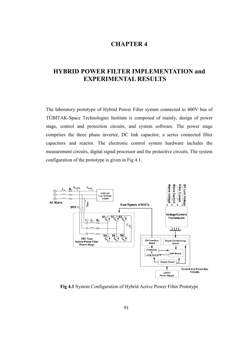
91
CHAPTER 4
4 HYBRID POWER FILTER IMPLEMENTATION and
EXPERIMENTAL RESULTS
The laboratory prototype of Hybrid Power Filter system connected to 400V bus of
TÜBĐTAK-Space Technologies Institute is composed of mainly, design of power
stage, control and protection circuits, and system software. The power stage
comprises the three phase inverter, DC link capacitor, a series connected filter
capacitors and reactor. The electronic control system hardware includes the
measurement circuits, digital signal processor and the protective circuits. The system
configuration of the prototype is given in Fig 4.1.
Fig 4.1 System Configuration of Hybrid Active Power Filter Prototype
92
4.1 Power Stage
The components used in the power stage of the prototype including power converter,
DC link capacitor and passive filter components are supplied by considering the
design criteria given in Section 3.3.
4.1.1 Power Converter
Three phase converter of the voltage source hybrid power filter is formed by using a
six pack Intelligent Power Module (IPM). Six pack IPM modules contain all six
IGBTs and their antiparalel diodes in a single package which simplifies the
complexity of the three phase converter.
Mitsubishi [58], Semikron [59], Infineon [60], Toshiba [22] and Fuji [24] are the
leading IGBT suppliers on the market, manufacturing six-pack IPM modules for
various applications such as compressors, fans/blowers, pumps, general purpose
drives, washing machines, etc. In the laboratory prototype, a flat base type 300A-
1200V IPM (Intelligent Power Module) of Mitsubishi Electric (PM300CLA120)
allowing a PWM switching frequency up to 20 kHz is used. Volt-Ampere rating of
the selected module is well above the current and voltage requirements indicated in
Section 3.3.2. The illustration of the module and inner connections are represented in
Fig 4.2. Technical details of the IPM are shown in Appendix A.

93
Fig 4.2 PM300CLA1200 IPM Module
4.1.2 DC Link Capacitor
The DC link capacitor used in simulation process is 7mF which results in a low
voltage ripple at DC link side. In the experimental set up, 7.05mF capacity is formed
by the parallel connection of 2.35 mF branches (Fig 4.3). Each 2.35 mF branch is
obtained by the series connection of 4700uF 400V aluminium electrolytic DC link
capacitors (ALS30A472NP400) to obtain a voltage rating of 800 VDC for a safe
operation in case of any fault. Moreover, the ripple current seen at the DC link is
shared by each 2.35mF branch, which reduces the power loss of each capacitor. As
indicated in Section 4.1.1, the voltage rating of the selected IPM is also above the
required voltage level. As a result, it is also possible to implement a conventional
voltage source Active Power Filter with the selected power converter and the
designed DC link configuration.
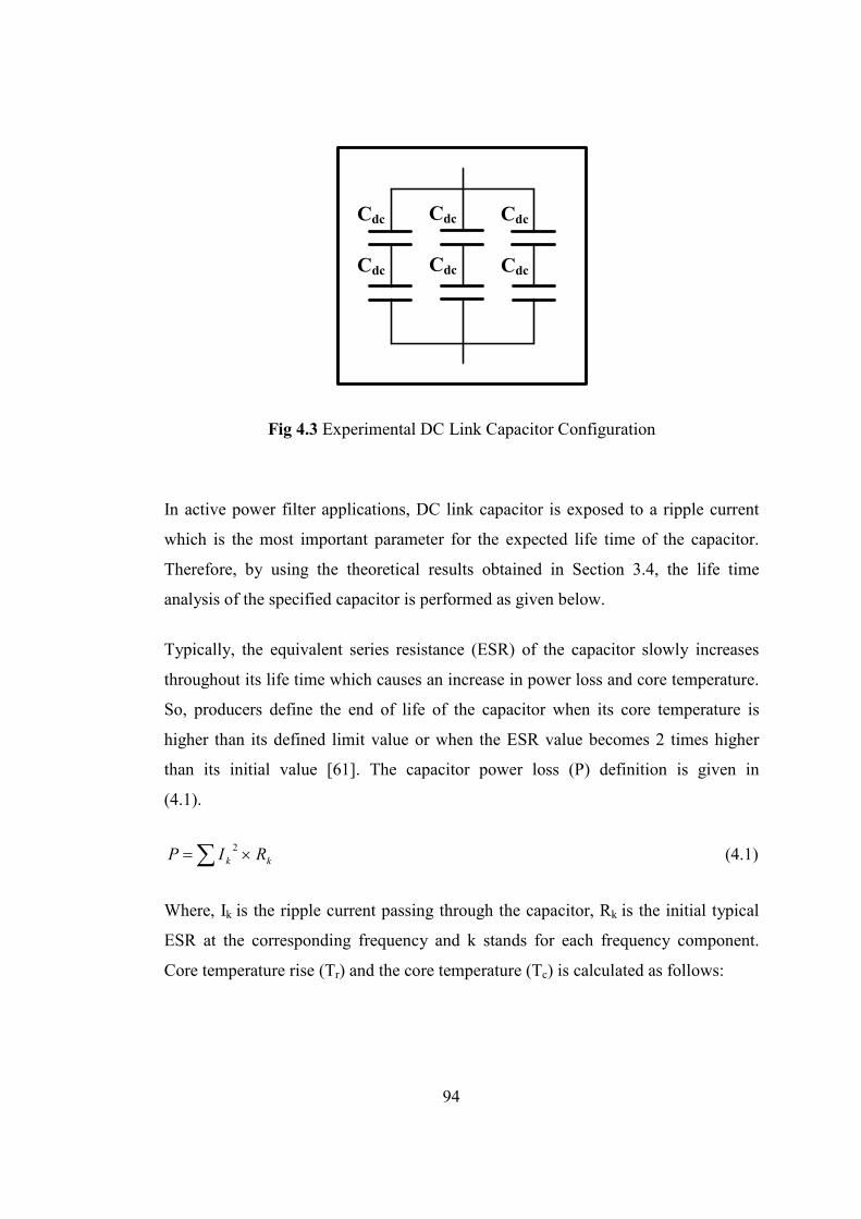
94
Cdc
Cdc
Cdc
Cdc
Cdc
Cdc
Fig 4.3 Experimental DC Link Capacitor Configuration
In active power filter applications, DC link capacitor is exposed to a ripple current
which is the most important parameter for the expected life time of the capacitor.
Therefore, by using the theoretical results obtained in Section 3.4, the life time
analysis of the specified capacitor is performed as given below.
Typically, the equivalent series resistance (ESR) of the capacitor slowly increases
throughout its life time which causes an increase in power loss and core temperature.
So, producers define the end of life of the capacitor when its core temperature is
higher than its defined limit value or when the ESR value becomes 2 times higher
than its initial value [61]. The capacitor power loss (P) definition is given in
(4.1).
kk RIP ×=∑ 2 (4.1)
Where, Ik is the ripple current passing through the capacitor, Rk is the initial typical
ESR at the corresponding frequency and k stands for each frequency component.
Core temperature rise (Tr) and the core temperature (Tc) is calculated as follows:

95
ca0
c
ha0
r
TT)C(T
PR)C(T
+=
×= (4.2)
Where, Rha (°C/Watt) is the thermal resistance of the capacitor, and Ta is the ambient
temperature. In Table 4.1, the ripple current of the DC link capacitor and the
corresponding ESR values obtained for 120V DC link is given (Section 3.4). The
core temperature and the core temperature rise are calculated by applying
(4.1) and (4.2).
Table 4.1 Ripple Current and Corresponding ESR Values
Frequency ESR Ripple Current
100Hz 11.6mΩ I1=0.1A
200Hz 8.5 mΩ I2=0.1A
300Hz 7.5 mΩ I3=10.5A
600Hz 6.5 mΩ I1=7.0A
W15.1m5.60.7m5.75.10m5.81.0m6.111.0P 2222 ≅×+×+×+×=
C645.215.13.2)C(T 00r =×=
C645.47645.245)C(T 00c =+=
The above calculations are made by assuming the following conditions:
Ambient Temperature (Ta): 45 °C
Forced Air Rate: 0 m/sec, and Rha = 2.3 °C/W
Although the power loss of the capacitor is so low, the life time of the capacitor is
also checked. At this ambient temperature and core temperature rise, the Le (Life
expectancy) is nearly 400 khrs and voltage factor KV is 1.21 which is given in [61].
So life expectancy of the capacitor is:

96
hours48400021.1450ExpectancyLife =×=
During the switching instants of IGBTs, voltage overshoots are observed due to the
stray inductances present in the power circuit. These voltage overshoots appear on
the DC link and seen across the power semiconductor. Thus, it should be checked
that, the maximum permissible blocking voltage of the semiconductor is not
exceeded. In order to limit these improper over voltages, the stray inductance
between the DC link capacitor and the power devices should be minimized by using
a laminated bus bar [62].
Thus, after selecting the voltage source inverter components properly, the laminated
copper busbar is designed for the connection of the DC link capacitors and IPM
terminals by using AutoCAD 2007 [63] (Fig A.1). 3D design of the laminated busbar
and the technical data of the aluminum electrolytic DC link capacitors capacitor are
provided in Appendix A.
4.1.3 Passive Filter Capacitor and Reactor
In Section 3.3.1 the filter capacitors are designed to have a 30kVAR capacity
theoretically. The filter capacitor is connected in series with the power converter for
each phase. Thus, it should withstand all the compensation current of the hybrid
power filter. However, the nominal current of the commercially available 30 kVAR
400 V low voltage AC capacitor units are not satisfying the required 70ARMS current
rating. As a result, AC filter capacitors shown in Fig 4.4 are provided from ABB.
Each capacitor (C) shown in Fig 4.4 is 48uF 400V rated AC filter capacitors. So
equivalent capacitance of one module can be obtained as follows:
uF288C6C ulemod =×=
Then the total capacity obtained by parallel connection of the two modules is:
uF576CCC 2ulemod1ulemodtotal =+=
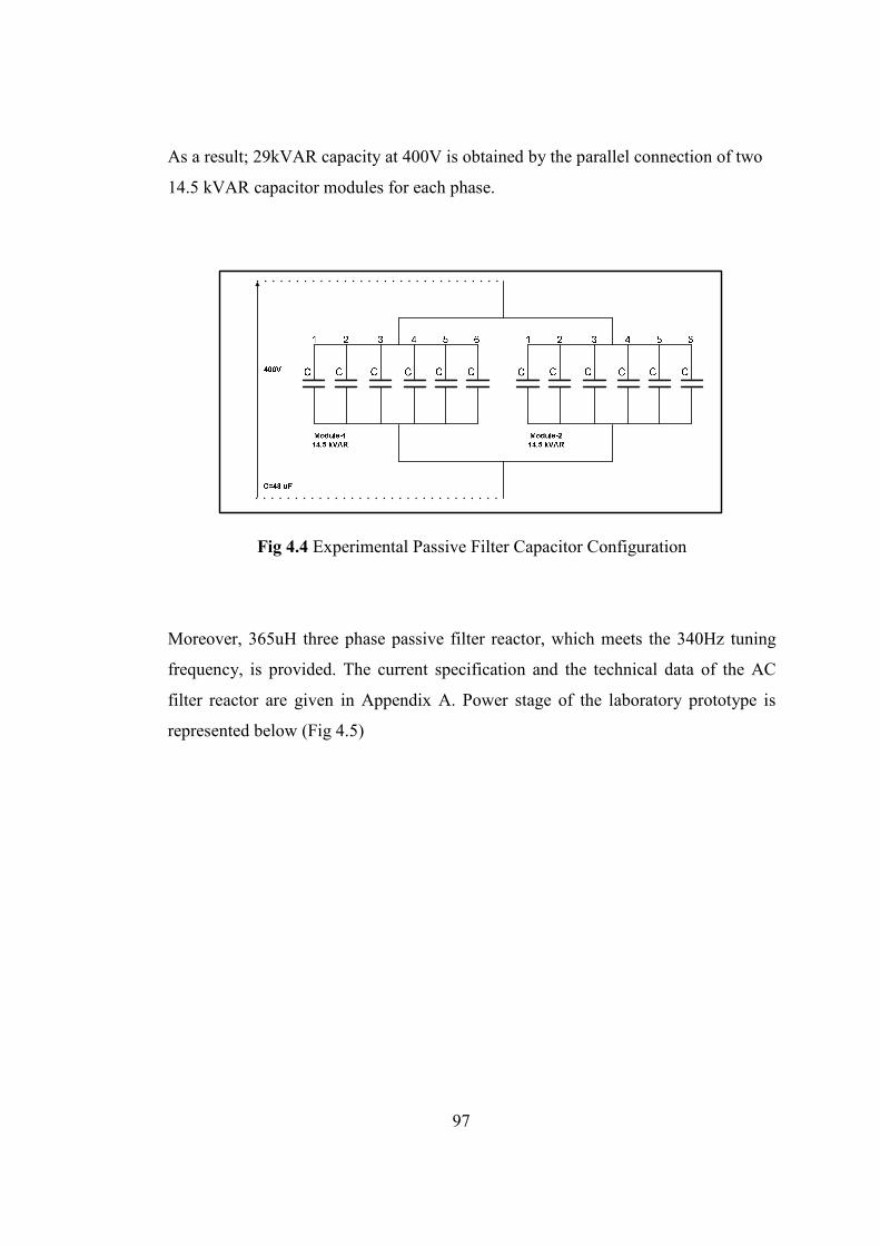
97
As a result; 29kVAR capacity at 400V is obtained by the parallel connection of two
14.5 kVAR capacitor modules for each phase.
Fig 4.4 Experimental Passive Filter Capacitor Configuration
Moreover, 365uH three phase passive filter reactor, which meets the 340Hz tuning
frequency, is provided. The current specification and the technical data of the AC
filter reactor are given in Appendix A. Power stage of the laboratory prototype is
represented below (Fig 4.5)

98
Fig 4.5 Power Stage of the Implemented Hybrid Power Filter Prototype
4.2 Control and Protection Circuits
The design criteria of control and protection circuits of the hybrid power filter are as
follows:
• To perform accurate measurement of the signals which are used in the control
system (Mains Voltage, Mains Current, Filter Current and DC Link Voltage)
• To generate the appropriate switching signals of the IPM module
• To protect system from unexpected faults (overvoltage at DC link, IPM fault,
emergency stop, etc.)
Control and protection circuits of the laboratory system can be divided into 4 groups:
measurement and signal conditioning boards, supply board, signal processing (DSP)
board, protection and firing boards (Fig 4.6).
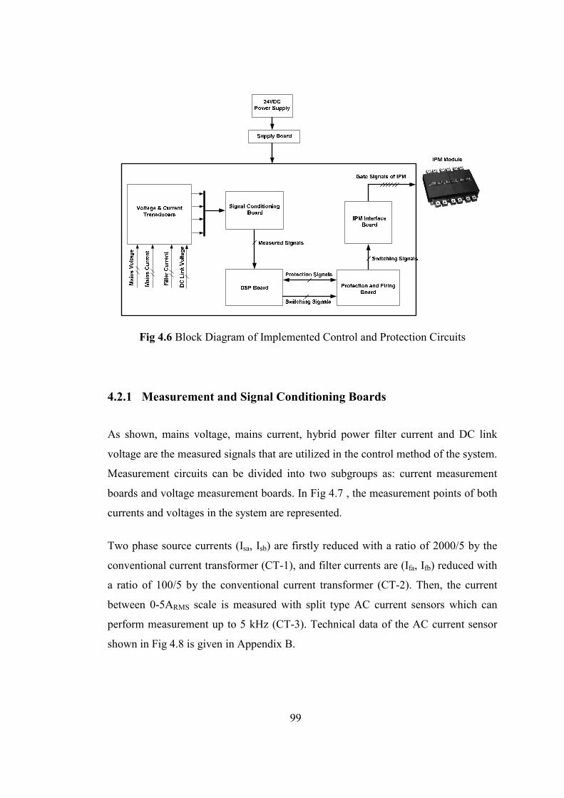
99
Fig 4.6 Block Diagram of Implemented Control and Protection Circuits
4.2.1 Measurement and Signal Conditioning Boards
As shown, mains voltage, mains current, hybrid power filter current and DC link
voltage are the measured signals that are utilized in the control method of the system.
Measurement circuits can be divided into two subgroups as: current measurement
boards and voltage measurement boards. In Fig 4.7 , the measurement points of both
currents and voltages in the system are represented.
Two phase source currents (Isa, Isb) are firstly reduced with a ratio of 2000/5 by the
conventional current transformer (CT-1), and filter currents are (Ifa, Ifb) reduced with
a ratio of 100/5 by the conventional current transformer (CT-2). Then, the current
between 0-5ARMS scale is measured with split type AC current sensors which can
perform measurement up to 5 kHz (CT-3). Technical data of the AC current sensor
shown in Fig 4.8 is given in Appendix B.

100
0.4 kV, 50 Hz
1.25 MVA
34.5/0.4kV
Vsa&Vsb
Ifa&Ifb
TUBITAK
Low Voltage
Loads
34.5 kV, 50 Hz
Isa&Isb
Vdc
CT-2
CT-3
CT-3
VT-1
VT-1
Hybrid Power
Filter
CT3: 3000/1 CTF-5A AC Current Sensor
CT-1: 2000/5A Current Transformer
VT-1: LV-25P Voltage Transducer
CT-1
CT2: 100/5A Current Transformer
Fig 4.7 Signal Measurement Points of Hybrid Power Filter System
Fig 4.8 CTF-5A AC Current Sensor

101
Two phase supply voltages (Vsa, Vsb) used in the PLL of the control method and the
DC link voltage are measured with a voltage transducer (LV25-P) which has a
measurement capability of DC, AC and pulsed signals. Technical data of the
employed voltage transducer is given in the Appendix B. The measured voltage
signals are transformed into a current signal between 0-25mA by the LEM board. By
signal conditioning board the current signals are transformed into voltage signals
which are processed in DSP board. The supply voltage is filtered digitally by a
second order low pass filter with a cut off frequency of 50Hz, and the DC link
voltage is filtered digitally by a first order low pass filter with a cut off frequency of
30Hz in digital signal processor. Moreover, the measured current signals are also
differentially amplified on the same signal conditioning board and transmitted to the
DSP board.
4.2.2 Supply Board
Supply board is designed by considering the supply requirements of the other
electronic boards. As a result the supply board is designed to produce the +15VDC, -
15VDC, +5VDC and +3.3VDC to provide the supply of DSP board, Signal
Conditioning and Measurement boards, IPM Interface board, Protection and Firing
Boards. The supply board is composed of DC-DC converters (LAMBDA PXF40-
24D15, PXE30-24S05, PXD20-24S3P3) which reduce 24VDC to the required DC
voltage levels. The 24VDC supply for the supply board is provided with a 100W
230VAC/24VDC DC power supply (LAMBDA HWS100-24/A). The detailed technical
data of the DC power supply is given in Appendix B.
4.2.3 Signal Processing (DSP) Board
In this thesis, the proposed control method is implemented on a 32 bit floating point
digital signal processor (DSP) of Texas Instruments. For this purpose, the evaluation

102
board of TMSF28335 is provided [64]. As shown in Fig 4.9 the evaluation board is
located on the designed DSP board. The DSP board includes the offset and buffer
circuits for analog/digital inputs to convert the input signals into 0-3V scale which
can be recognized by DSP itself. Digital outputs of the DSP are converted from 0-3V
to 0-5V scale which is processed by the protection and firing board.
The 150 MHz processor, single precision floating point unit, 12.5MHz 16 channel-12
Bit Analog/Digital Converter unit, prepared sine table in ROM, enhanced PWM
module are the main advantages of the used TMSF28335 DSP. The main properties
of the floating point digital signal processor are also given in Appendix B.
4.2.4 Protection and Firing Boards
In order to operate the system in a safe manner, some analog and digital faults are
produced in the system. If the DC link voltage exceeds the predefined limit value,
DC link voltage fault is produced. It is the most probable fault that may occur in the
initial tests of the system. In the vicinity of a control supply under voltage, over
temperature, over current and short circuit, IPM fault signal is produced by the IPM
internal gate control circuits. Furthermore, if one of the voltage level produced by the
supply board goes below the required voltage level a Supply fault is produced. All of
the produced fault signals are latched and passed through an AND logic to produce a
global fault called as System Fault. When the system produces a system fault, the
upper IGBTs of the IPM are forced to turn on and lower IGBTs of the IPM are
forced to turn OFF by the protection board. As shown in Fig 4.6, switching signals
are produced by DSP and transferred to the protection and firing board for protection
purposes as described above. However another electronic board called IPM interface
board is needed to meet the IPM logic level requirements. Therefore, IPM interface
board which is directly mounted on IPM pins is designed to provide opto-coupled
isolation for control signals and to assure isolated power supplies for the IPM’s built-
in gate drive and protection circuits [65]. Implemented control and protection circuits

103
of the hybrid power filter prototype are given in Fig 4.9. The power stage and the
control system of the hybrid power filter are mounted on the same panel by
separating them with a divider panel. The overall configuration of the system is
represented in Fig 4.10.
Fig 4.9 Control and Protection Circuits of the Implemented Hybrid Power Filter Prototype

104
Fig 4.10 Implemented Hybrid Power Filter Prototype
4.3 Software of the Prototype
As described above, the proposed control method is implemented on DSP
TMSF28335. The software is developed by Code Composer Studio IDE of Texas
Instruments (ANSI C/C++). The flowchart of the software developed by code
composer studio is given in Appendix C.
If DSP senses the hardware RESET, firstly the initialization procedure is completed.
Initialization procedure includes the initialization of constants, definition of
functions, definition of variables, configuration of DSP registers, configuration of
peripherals (PWM module) and initial value assignment of variables.
After initializations are completed, the DSP waits for the START signal. During this
time period, offset of the ADC channels is calculated and calibration of the signals is

105
done to obtain the original signal magnitudes. When the START signal is sent to the
DSP, the program branches to the main part. All the calculations represented in the
proposed voltage reference generation method (Section 2.2.2.2.2) and PLL are
implemented in the main part. LPFs used to extract the harmonic component are
implemented digitally in terms of mean calculation.
The sampling period of the digital controller is chosen as 40us. The ePWM feature of
the TMSF28335 also allows user to implement Sinusoidal Pulse Width Modulation
easily at 10 kHz switching frequency [66].
4.4 Experimental Results
In this part of the thesis, the experimental results obtained for Hybrid Active Power
Filter which is implemented with the proposed control method (Section 2.2.2.2.2) are
given. Moreover, a method which is used to compensate the phase errors of the
current measurement devices (CT-1) is investigated. The startup procedure of the
laboratory prototype is same with the simulation model of the system (Section 3.4).
When hybrid power filter is OFF, the distorted current waveform of the source side is
as shown in Fig 4.11. The frequency spectrum of the source current (Fig 4.12) shows
that the harmonic content is slightly higher than the measurement results given in
Section 3.1 which is an expected result due to a possible increase in computer loads.
As expected 3rd, 5th, 7th and 11th are the most dominant harmonic components to be
eliminated. However, 3rd harmonic component is out of the scope of the designed
hybrid power filter system due to its 3 phase-3 wire connection topology. Initially,
the circuit breaker (BRK1) is turned ON and only the passive filter is operated (Fig
4.13, Fig 4.14).

106
Fig 4.11 Experimental Waveforms when Hybrid Power Filter is OFF C3: Supply Voltage (100V/div), C4: Supply Current (200A/div)
Fig 4.12 Frequency Spectrum of Source Current When Hybrid Power Filter is OFF

107
Fig 4.13 Experimental Waveforms when only Passive Filter is ON C2: Filter Current (40A/div), C3: Supply Voltage (100V/div) C4: Source Current (200A/div), F1: Load Current (200A/div)
Fig 4.14 Load Current and Source Current when only Passive Filter is ON

108
Then the DC link capacitor voltage is built up and set to its reference 60V. The
transient response of the system shows that, DC link voltage reaches to 60V with an
overshoot of nearly 20V and kept constant at its reference value. The experimental
waveforms obtained, as the hybrid power filter is turned on are given below.
Fig 4.15 C1: DC Link Voltage (20V/div), C2: Filter Current (40A/div)

109
Fig 4.16 F1: Load Current (200A/div), C2: Filter Current (40A/div) C3: Supply Voltage (100V/div), C4: Source Current (200A/div)
Fig 4.17 C1: DC Link Voltage (10V/div), C2: Filter Current (40A/div) C4: Source Current (200A/div), F1: Load Current (200A/div)

110
Currents I1 I3 I5 I7 I9 I11 I13 I17
Load 330.4A 16.2A 34.9A 13.9A 3.3A 7.4A 0.8A 1.24A
Source 302.3A 16.0A 6.4A 3.54A 3.4A 5.8A 0.7A 1.22A
Filter 45.4A - 29.7A 13.8A - 7.5A 0.7A 0.2A
Fig 4.18 Frequency Spectrum of Load, Source and Filter Current
When hybrid power filter is turned on with the proposed control method, the most
dominant 5th, 7th and 11th harmonics are reduced and source current seems to be
sinusoidal as shown in Fig 4.16 and Fig 4.17. However, the frequency spectrum of
the load, source and filter current shows that, the performance of the system is not
satisfactory. Theoretically, hybrid power filter should inject the calculated harmonic
content of the load current in same magnitude but with opposite phase. However, the
experimental results obtained in Fig 4.18 show that, the injected filter current (IFh) is
not completely in opposite phase with the load current harmonic content (ILh). After
analyzing the obtained data for various cycles, it is observed that the conventional
2000:5A current transformer (CT-1 in Fig 4.7) used for the measurement of the
source current results in a phase difference Ø which also increases with increasing
harmonic order. In order to compensate the indicated phase error (Ø), a phase
compensation method is introduced and digitally implemented as given below. The
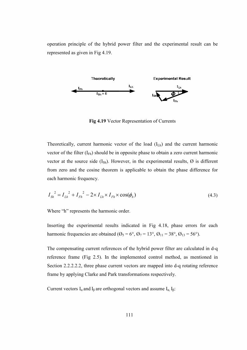
111
operation principle of the hybrid power filter and the experimental result can be
represented as given in Fig 4.19.
Fig 4.19 Vector Representation of Currents Theoretically, current harmonic vector of the load (ILh) and the current harmonic
vector of the filter (IFh) should be in opposite phase to obtain a zero current harmonic
vector at the source side (ISh). However, in the experimental results, Ø is different
from zero and the cosine theorem is applicable to obtain the phase difference for
each harmonic frequency.
)cos(2222
hFhLhFhLhSh IIIII φ×××−+= (4.3)
Where “h” represents the harmonic order.
Inserting the experimental results indicated in Fig 4.18, phase errors for each
harmonic frequencies are obtained (Ø5 = 6°, Ø7 = 13°, Ø11 = 38°, Ø13 = 56°).
The compensating current references of the hybrid power filter are calculated in d-q
reference frame (Fig 2.5). In the implemented control method, as mentioned in
Section 2.2.2.2.2, three phase current vectors are mapped into d-q rotating reference
frame by applying Clarke and Park transformations respectively.
Current vectors Iα and Iβ are orthogonal vectors and assume Iα, Iβ:
112
)sin(I
)cos(I
θ=
θ=
β
α (4.4)
Applying Park transformation matrices to unity current vectors as given in (2.22);
βα
βα
×+×=
×−×=
I)wtcos(I)wtsin(I
I)wtsin(I)wtcos(I
q
d (4.5)
So;
)sin()wtcos()cos()wtsin(I
)sin()wtsin()cos()wtcos(I
q
d
θ×+θ×=
θ×−θ×= (4.6)
Rearranging (4.6);
)wtsin(I
)wtcos(I
q
d
+θ=
+θ= (4.7)
Id and Iq vectors can be shifted on the same reference frame by adding the phase delay
Ø and new shifted vectors Id’ and Iq
’ are obtained as shown in (4.8).
)sin()wtcos()cos()wt(sin)wtsin(
)sin()wtsin()cos()wtcos()wtcos(
'qI
'dI
φ×+θ+φ×+θ=φ++θ=
φ×+θ−φ×+θ=φ++θ= (4.8)
Where; )wtsin(I
)wtcos(I
q
d
+θ=
+θ=
So, shifted new vectors Id’ and Iq
’ can be obtained in terms of Id
and Iq.
)sin(I)cos(I)wtsin(I
)sin(I)cos(I)wtcos(I
dq
'
q
qd
'
d
φ×+φ×=φ++θ=
φ×−φ×=φ++θ= (4.9)

113
Therefore the phase errors of each harmonic component (Id5, Iq5, Id7, Iq7, Id11, Iq11, Id13,
Iq13) on d-q reference frame (Fig 2.12) can be compensated by applying a simple
phase delay calculation represented in (4.9). After utilizing the phase compensation
method, the following waveforms are observed experimentally.
Fig 4.20 and Fig 4.22 shows that the DC link voltage of the Hybrid power filter is
kept constant at 60VDC and the source current becomes nearly a pure sinusoidal. It
is clear from Fig 4.23 that, the supply voltage and current is not in phase. The
reactive power compensation capacity is limited (30kVAR) with the capacity of the
utilized passive filter. In order to obtain a unity power factor, the passive filter
capacitor should be increased which will increase the size and the cost of the system.
Moreover, the hybrid active power filter is designed and implemented mainly for the
elimination of the most dominant current harmonics.
Fig 4.20 DC Link Voltage (10V/div), C2: Filter Current (40A/div) C4: Source Current (200A/div), F1: Load Current (200A/div)

114
Fig 4.21 C2: Filter Current (40A/div), C3: Supply Voltage (100V/div) C4: Source Current (200A/div), F1: Load Current (200A/div)
Fig 4.22 C1: DC Link Voltage (10V/div), C2: Filter Current (40A/div) C4: Source Current (200A/div), F1: Load Current (200A/div)

115
18°39°
Fig 4.23 C2: Filter Current (40A/div), C3: Supply Voltage (100V/div) C4: Source Current (200A/div), F1: Load Current (200A/div)
Addition of phase error compensation greatly improves the filtering performance of
the system. The frequency spectrum of the source current proves that (Fig 4.24) the
most dominant 5th, 7th and 11th harmonics are suppressed to satisfy the current
distortion limits indicated in Table 1.2. The 13th harmonic component is already
below the limit value, so that it is excluded in the current reference calculation.
The DC link voltage of the hybrid power filter is quite low when compared with a
conventional voltage source Active Power Filter. In the implemented system, DC
link voltage is kept constant at 60VDC. As a result, the rating of the power converter
is greatly reduced. In fact, two definitions (SVSC,max, SVSC,installed) can be made for the
volt-ampere rating of the power converter. SVSC,max is the maximum converter
capacity which shows the capability of the power converter for the specified DC link
voltage level. Whereas, SVSC,installed is used to indicate the amount of power occupied
while compensating the harmonic content of the experimental load given in Fig
4.24.

116
Currents I1 I3 I5 I7 I9 I11 I13 I17
Load 311.7A 11.4A 32.1A 11.3A 3.2A 7.0A 0.8A 1.5A
Source 289.4A 11.5A 5.1A 1.2A 3.1A 0.5A 0.8A 1.5A
Filter 45.8A - 27.1A 11.4A - 7.2A - -
Fig 4.24 Frequency Spectrum of Load, Source and Filter Current
Fig 4.25 Single Line Diagram of the Hybrid Power Filter

117
The maximum converter capacity is defined as below:
maxfilter,maxterminal,maxVSC, IV3S ××= (4.10)
However, to determine the maximum terminal voltage of the converter and the
maximum filter current the following constraints should be satisfied. Firstly, the
voltage appearing across the capacitor (Vcap) should not exceed the nominal voltage
of the selected AC capacitors (4.11). Then, the nominal current rating of the filter
reactor should be met (4.12). Finally, in order to generate the required compensation
currents, (4.13) should be satisfied.
nominalCap,hC,
n
1hfilter, )(I VZ
h
<×∑=
(4.11)
nominalL,
n
1
2hfilter, )(I I
h
<∑=
(4.12)
DC
^
hFilter,1
hF, VIZn
h
<×∑≠
(4.13)
In (4.11), (4.12), and (4.13) h represents the order of the harmonic, Ifilter,h is the filter
current, ZC,h is the impedance of the capacitor and ZF,h is the impedance of the LC
filter at the corresponding harmonic frequency. As explained in Section 4.1.3, the
filter reactor is selected to have a 70ARMS nominal current rating. 45ARMS of this
current is the fundamental current flow due to the filter capacitor. So, the maximum
harmonic current that the hybrid filter can withstand is limited by the filter reactor as
50ARMS (4.14).
RMSAI 504570 22h(max)Filter, =−= (4.14)
In the implement system, the most dominant 5th, 7th, and 11th current harmonics are
eliminated. The impedances of the experimentally used passive filter (Section 4.1.3)

118
at 50 Hz, 250 Hz, 350 Hz and 550 Hz are given in (4.15). Then, the terminal voltage
can be expressed as given in (4.16), by assuming zero fundamental voltage at the
terminal of the voltage source converter. So, the maximum terminal voltage can be
obtained by assuming the all harmonic content (50ARMS) appearing at 550Hz as a
worst case.
Ω=
Ω=
Ω=
Ω=
78.0
044.0
487.0
19.5
F,11
F,7
F,5
F,1
Z
Z
Z
Z
(4.15)
So, the constraint given in (4.13) is checked with Ifilter,11=50ARMS and ZF,11=0.78Ω.
V60VV5525078.0IZ DCFilter,11F,11 =<=××=×
2hFilter,
1hF,min )( IZV
n
h
alter ×= ∑≠
(4.16)
V395078.0IZV max,Filter11,Fmax,alminter =×=×= (4.17)
By using equation (4.10) the maximum converter rating at 60VDC link is obtained as
given below:
kVA7.407933S maxVSC, ≅××=
Then, by using the current spectrum given in Fig 4.24 and the impedances shown in
(4.15), the installed rating of the voltage source converter can be easily found as
below:
RMS2222
n
1h
2hfilter, A23.542.74.111.2745)(I =+++=∑
=

119
RMS222
alminter V35.14)78.02.7()044.04.11()487.01.27(V =×+×+×=
kVA35.123.5435.143IV3S RMS,filteralminterledVSC,instal ≅××=××=
If the harmonics of the load indicated in Fig 4.24 were filtered by a conventional
VSC type APF, the required DC link would be around 700 VDC which increases the
losses and the rating of the power converter [56]. However, the total rating of the
hybrid power filter (SHPF) by including the passive filter is higher than the rating of
the conventional VSC type active power filter (SAPF), due to the unavoidable
fundamental current flow as shown in (4.18) and (4.19)
kVA5.48704003IV3S RMS,filterSHPF ≅××=××= (4.18)
kVA6.34504003IV3S RMS,filterSAPF ≅××=××= (4.19)
Although the overall rating of the hybrid power filter is higher, the reduction in the
converter rating is a significant benefit in terms of losses. Moreover, it provides the
opportunity of employing low rated IGBTs or even MOSFETs in the converter
design. Even though no additional switching filter is used, high frequency current
ripples are also minimized with the applied system. Moreover, experimental results
have shown the effectiveness of the proposed control method which is also simple to
implement. As a result, the advantages listed above show that especially for large
power applications, Hybrid active power filters are seem to be an appropriate
solution with their reduced DC link voltages.

120
CHAPTER 5
5 CONCLUSIONS & FURTHER WORK
In this research work, the design and implementation of a three phase shunt
connected Hybrid Active Power Filter has been carried out. The prototype has been
designed and developed to eliminate most dominant harmonics existing at
TÜBĐTAK-Space Technologies Institute 400V low voltage line.
The developed prototype is composed of a three phase voltage source converter with
PWM modulation and a series connected LC passive filter tuned at 340Hz. The
amplification phenomenon of the shunt connected passive filter is suppressed by the
applied hybrid filter topology. The 5th, 7th and 11th harmonics are greatly reduced and
the line currents have become to comply with IEEE Std. 519-1992. The DC link
voltage of the VSC is also significantly decreased as compared with a conventional
shunt connected VSC Active Power Filter. The reduction of the DC link voltage also
assures low rated converter and lower losses.
Moreover, the conventional control method applied for transformerless hybrid power
filters are analyzed [29, 33, 35]. The feedback and the feedforward control methods
are effective to eliminate the current harmonics of a three phase diode rectifier load.
However, the existence of voltage harmonics at the source side affects the
performance. Hence, a voltage feedforward method is introduced and verified by
simulation results to isolate the supply side voltage harmonics.
The developed laboratory prototype is designed to eliminate the most dominant
harmonics of the distorted line current of TÜBĐTAK. It is observed by measurement
results that unbalanced 3rd harmonic components are also available at the source side.

121
However, the developed hybrid active power filter topology cannot eliminate these
150Hz components with a three phase three wire connection. Hence, a voltage
reference generation method is proposed to exclude the third harmonic components
during the reference current calculation. The proposed method is digitally
implemented and verified by both simulation and experimental results.
Furthermore, it is observed that, conventional current transformers perform accurate
measurement in terms of magnitude but not in terms of phase. Therefore, the
proposed control method is updated to compensate the phase error of the
conventional current transformers which are used to measure the source current.
Following conclusions can be drawn from the results of theoretical and experimental
work of this research work:
• The DC link voltage and the volt-ampere rating of the power converter of
VSC based Active Power Filter is greatly reduced with the developed
Hybrid Power Filter topology.
• The reduced DC link voltage allows designers to use lower rated IGBTs,
or MOSFETs at lower costs.
• Although the switching frequency is 10 kHz in the implemented system,
the hybrid power filter current is ripple free, and no additional switching
ripple filter is required.
• The reactive power compensation capability is limited with the capacity of
the employed passive filter capacitor. This criterion may limit the
application of hybrid power filters where, both current harmonic
elimination and reactive power compensation are crucial.
• The resonance risk of the existing passive filters can be damped by
utilizing hybrid power filter topology with reduced converter ratings.

122
• The applied topology provides direct connection of Active Power Filters to
the mains side in high power applications without using a coupling
transformer.
In this research work, the experimental results of the implemented hybrid power
filter prototype are given for the proposed voltage reference generation method to
exclude the 3rd harmonic current components. However, theoretically proposed
voltage feedforward method has not been verified by experimental results yet. The
implemented system can be operated to filter the harmonics of a thyristor controlled
rectifier load. By utilizing a thyristor rectifier load, the phase angle of the load can be
changed with respect to the voltage harmonics phase. Therefore, the experimental
verification of the proposed voltage feedforward method can be stated as a future
work.
The developed hybrid power filter prototype assures satisfactory filtering results with
a reduced DC link voltage. Nevertheless, a complete comparison between a
conventional VSC type active power filter and the hybrid power filter is not
included. The ratings of the IPM module and DC link capacitors are suitable to be
operated as a conventional VSC type APF; by only changing the series LC filter with
an appropriate filter reactor. Therefore, an exact analysis can be performed between
these two topologies in terms of loss, cost and filtering performance.

123
REFERENCES
[1] IEEE Std. 519-1992, “IEEE Recommended Practices and Requirements for
Harmonic Control in Electrical Power Systems”
[2] IEEE Std. 519-1981, “Guide for Harmonic Control and Reactive Power
Compensation of Static Power Converters”
[3] B. Singh, K. Al-Haddad, A. Chandra, “A Review of Active Power Filters for
Power Quality Improvements,” IEEE Trans. on Industrial Electronics, Vol.
46, No. 5, pp. 960-971, Oct. 1999
[4] R. D. Henderson, P. J. Rose, “Harmonics: The effects on power quality and
transformers,” IEEE Transactions on Industry Applications, vol. 30, no. 3, pp.
528-532, May/June 1994
[5] A. Elmoudi, M. Lehtonen, H. Nordman “Effect of harmonics on transformers
loss of life,” Conference Record of the IEEE International Symposium on
Electrical Insulation, pp. 408-411, 2006
[6] IEC Norm 555-3 prepared by the International Electrical Commission
[7] Elektrik Piyasasında Dağıtım Sisteminde Sunulan Elektrik Enerjisinin
Tedarik Sürekliliği, Ticari Ve Teknik Kalitesi Hakkında Yönetmelik,EMRA,
2006 (in Turkish)
[8] Elektrik Đletim Sistemi Arz Güvenilirliği veKalitesi Yönetmeliği, EMRA,
2007 (in Turkish)
[9] S. N. AL. Yousif, M. Z. C. Wanik, A. Mohammed, “Implementation of
Different Passive Filter Designs for Harmonic Mitigation”, National Power &
Energy Conference (PECon) Proceedings, Malaysia, pp. 229-234, 2004

124
[10] Damian A. Gonzalez, John C. Mccal, “Design of Filters to Reduce Harmonic
Distortion in Industrial Power Systems”, IEEE Trans. On Industry
Applications, Vol. IA-23, No. 3, pp. 504-511, May/June 1987
[11] J. C. Das, “Passive Filters, Potentialities and Limitations”, IEEE Trans. On
Industry Applications, Vol. 40, No. 1, pp. 232-241, Jan/Feb 2004
[12] H. Sasaki, T. Machida, “A New Method to Eliminate AC Harmonic Currents
by Magnetic Flux Compensation-Consideration on Basic Design,” IEEE
Trans. Power App. Syst., Vol. 90, No. 5, pp. 2009-2019, Sep./Oct. 1971
[13] H. Kawahira, T. Nakamura, S. Nakazawa, “Active Power Filters”, IEEJ
IPEC-Tokyo, pp. 981-992, 1983
[14] H. Akagi, H. Fujita, “A New Power Line Conditioner for Harmonic
Compensation in Power Systems”, IEEE Trans. On Power Delivery, Vol. 10,
No. 3, pp. 1570-1575, July 1995
[15] D. Chen, S. Xie, “Review of the Control Strategies Applied to Active Power
Filters,” IEEE International Conf. on Electric Utility Deregulation,
Restructuring and Power Tech., pp. 666-670, April 2004
[16] Y. Hayachi, N. Sato, K. Takahashi, “A Novel Control of a Current Source
Active Filter for AC power system harmonic compensation,” IEEE Trans. on
Industry App., Vol. 27, No. 2, pp. 380-384, 1991
[17] H. Akagi, “Active Harmonic Filters,” Proceedings of the IEEE, Vol. 93, No.
12, pp. 2128-2141, Dec. 2005
[18] H. Özkaya, “Parallel Active Filter Design, Control, and Implementation”,
M.S. Thesis Electrical and Electronics Engineering Middle East Technical
University, June 2007

125
[19] L. Benchaita, S. Saadate, A. Salemnia, “A comparison of voltage source and
current source shunt active filter by simulation and experimentation,” IEEE
Trans. on Power Systems, Vol. 14, No. 2, pp. 642-647, May 1999
[20] V. B. Bhavaraju, P. Enjeti, “A novel active line conditioner for a three-phase
system,” in Proc. IEEE IECON’93, Vol. 2, pp. 979-985, Oct. 1993
[21] A. D. le Roux, Hd. T. Mouton, H. Akagi “Digital control of an integrated
series active filter and diode rectifier with voltage regulation,” IEEE Trans.
On Industry Applications, Vol. 39, Iss. 6, pp. 1814-1820, Nov. /Dec. 2003
[22] “TOSHIBA [Online],” http//www.toshiba.co.jp, last visited on 25/08/2009
[23] “ABB [Online],” http//www.abb.com, last visited on 25/08/2009
[24] “Fuji Electric Group [Online],” http//www.fujielectric.com, last visited on
25/08/2009
[25] L. A. Moran, J. W. Dixon, J. R. Espinoza and R. R. Wallace, “Using Active
Filters To Improve Power Quality”, 5th Brazilian Power Electronics
Conference, COBEP’99
[26] F. Z. Peng, H. Akagi, A. Nabae “A new approach to harmonic compensation
in power systems,” in Conf. Rec. IEEE-IAS Annu Meeting, Vol. 1, pp. 874-
880, Oct. 1988
[27] H. Fujita, H. Akagi “A practical approach to harmonic compensation in
power systems-series connection of passive and active filters,” in Conf. Rec.
IEEE-IAS Annu Meeting, Vol. 2, pp. 1107-1112, Oct. 1990
[28] L.Chen, A.V.Jouanne “A Comparison and Assessment of Hybrid Filter
Topologies and Control Algorithms” IEEE Power Electronics Specialists
Conference, Vol. 2, pp 565-570, 2001

126
[29] H. Akagi “A medium voltage transformerless AC/DC Power Conversion
System Consisting of a Diode Rectifier and a Shunt Hybrid Filter” IAS
annual meeting, Vol. 1, pp 78-85, Oct. 2002
[30] C. A. Quinn, N. Mohan, “Active filtering of harmonic currents in three-phase,
four-wire systems with three-phase, single-phase nonlinear loads,” in Proc.
IEEE APEC’92, pp. 829–836, 1992
[31] P. Enjeti, W. Shireen, P. Packebush, and I. Pitel, “Analysis, design of a new
active power filter to cancel neutral current harmonics in three phase four-
wire electric distribution systems,” in Conf. Rec. IEEE-IAS Annu. Meeting,
Vol. 30, pp. 939–946, Feb.1993
[32] H. Özkaya, O.S. Şentürk, A.M. Hava, “Üç fazlı paralel etkin süzgecin akım
denetim yöntemleri” ELECO 2006, Elektrik-Elektronik-Bilgisayar
Mühendisliği Sempozyumu, 6-10 Aralık 2006, Bursa, sayfa 121-125
[33] H. Özkaya, O.S. Şentürk, A.M. Hava, “Performance enhancement of discrete
time hysteresis current regulators and comparison with linear current
regulators for parallel active filters,” IEEE-IEMDC 2007 Conference,
Antalya, Turkey, Vol.2, pp. 1282-1287, May 2007
[34] W. Tangtheerajaroonwong, T. Hatada, K. Wada, H. Akagi, “Design of a
Transformerless Shunt Hybrid Filter Integrated into a Three Phase Diode
Rectifier”, PESC’06, pp. 1-7, June 2006
[35] R. Inzunza, H. Akagi, “A 6.6 kV Transformerless Shunt Hybrid Active Filter
for Installation on a Power Distribution System”, IEEE Trans. On Power
Electronics, Vol. 20, No. 4, pp. 893-900, July 2005

127
[36] G. D. Marques, “A Comparison of Active Power Filter Control Methods in
Unbalanced and Non-sinusoidal Conditions”, Proceedings of IECON, Vol. 1,
pp. 444-449, 1998
[37] S: D. Round, D. M. E. Ingram, “An Evaluation of Techniques for
Determining Active Filter Compensating Currents in Unbalanced Systems”,
Proc. European Conf. on Power Electronics and Applications, Vol. 4, pp.
767-772, Trondheim, 1997
[38] S. Rechka, E. Ngandui, J. Xu, P. Sicard, “A comparative Study of Harmonic
Detection Algorithms for Active Filters and Hybrid Active Filters”, Power
Elects. Specialists Conf., Vol. 1, pp. 357-363, 2002
[39] G. W. Chang, T. C. Shee, “A Comparative Study of Active Power Filter
Reference Compensation Approaches”, Power Engineering Society Summer
Meeting, Vol. 2, pp. 1017-1021, 2002
[40] L. Asiminoaei, F. Blaabjerg, S. Hansen, “Evaluation of Harmonic Detection
Methods for Active Power Filter Applications”, Applied Power Elects. Conf.
and Expo., Vol. 1, pp. 635-641, 2005
[41] A. M. Massoud, S. J. Finney, B. W. Williams, “Review of Harmonic Current
Extraction Techniques for an Active Power Filter”, International Conf. on
Harmonics and Quality of Power, Vol. 1, pp. 154-159, 2004
[42] J. M. M. Ortega, M. P. Esteve, M. B. Payan, A. G. Exposito, L. G. Franguelo,
“Reference Current Computation Methods for Active Power Filters:
Accuracy Assessment in the Frequency Domain”, IEEE Trans. on Power
Electronics, Vol. 20, No. 2, pp. 446-456, 2005

128
[43] H. Akagi, Y. Kanazawa, A. Nabae, “Generalized theory of instantaneous
reactive power and its applications,” Transactions of the IEEE Japan, Part B,
Vol. 103, No. 7, pp. 483-490, 1983
[44] H. Akagi, Y. Kanazawa, A. Nabae, “Generalized theory of the instantaneous
reactive power in three phase circuits,” IPEC’83 International Power
Electronics Conference, Tokyo, Japan, pp. 1375-1386, 1983
[45] H. Akagi, Y. Kanazawa, A. Nabae, “Instantaneous reactive power
compensator comprising switching devices without energy storage
components,” IEEE Trans. Ind. Appl., Vol. 1A-20, No. 3, pp. 625-630, 1984
[46] H. Akagi, E. H. Watanabe, M. Aredes, “Instantaneous Power Theory and
Applications to Power Conditioning”, Book IEEE Press, pp. 41-102, 2007
[47] S.Bhattacharya, T.M. Frank, D.M. Divan, and B. Banerjee “Active Filter
System Implementation” IEEE Industry Applications Magazine, Vol. 4, pp.
47- 63, 1998
[48] A. Altintas, O. Bingol, “The Evaluation and Comparison of Mathematical
Models Utilized in Active Power Filters” Suleyman Demirel Üniversitesi Fen
Bilimleri Enstitüsü Dergisi pp 145-150, 2004 (Originally in Turkish)
[49] S. K. Chung, “A Phase Tracking System for Three Phase Utility Interface
Inverters”, IEEE Trans. On Power Electronics, Vol. 15, pp. 431-438, May
2000
[50] V. Kaura, V. Blasko, “Operation of a Phase Locked Loop System Under
Distorted Utility Conditions”, IEEE Trans. On Industry Applications, Vol. 33,
pp. 58-63, Jan./Feb. 1997

129
[51] L. R. Limongi, R. Bojoi, “New Control Strategy for Hybrid Power Filters
Using Sinusoidal Signal Integrators for Current Reference Generation”, IAS
Annual Meeting Conference Record, pp. 1636-1643, Sept. 2007
[52] O.Ucak, Đ.Kocabas, A.Terciyanlı “Design and Application of a Hybrid Active
Power filter with Supply Side Harmonics Isolation”, PCIM Conference, pp.
2008
[53] EMTDC/PSCAD 4.2.0 Professional. A Power System and Power Electronics
time domain transient simulation software, MONITOBA-HVDC Research
Centre, 2005
[54] Ansoft-Simplorer V7.0. A power electronics simulation software, Ansoft
Corporation, 2004
[55] Matlab 6.5. A numerical computation software, Mathworks Inc., 2002
[56] H. Akagi, S. Srianthumrong, Y. Tamai, “Comparisons in Circuit
Configuration and Filtering Performance between Hybrid and Pure Shunt
Active Filters”, Industry Applications Conference, Vol. 2, pp. 1195-1202,
2003
[57] Đ.Kocabas, O.Ucak, A.Terciyanlı, “DSP Based Voltage Source Paralel Active
Power Filter Implementation”, Eleco, pp 171-175, 2006 (Originally in
Turkish)
[58] “POWEREX [Online],” http//www.infineon.com, last visited on 12/08/2009
[59] “SEMIKRON [Online],” http//www.semikron.com, last visited on
12/08/2009
[60] “INFINEON [Online],” http//www.infineon.com, last visited on 12/08/2009

130
[61] BHC Capacitors Application Notes TD001-003 pp. 16-26
[62] M. C. Caponet, F. Profumo, R. W. D. Doncker, A. Tenconi, “Low Stray
Inductance Bus Bar Design and Construction for Good EMC Performance in
Power Electronics Circuits”, IEEE Trans. On Power Electronics, Vol. 17, pp.
225-231, March 2002
[63] AutoCAD 2007. A 2D and 3D design and drawing software, Autodesk
[64] “eZdspTM F28335 Technical Reference”, Spectrum Digital, Inc. September
2007
[65] “BP7A-L-Series IPM Interface Circuit Reference Design”, Powerex,
February 2005
[66] TMS320x28xx, 28xxx Enhance Pulse Width Modulator (ePWM) Module
Reference Guide

131
APPENDIX A
TECHNICAL DATA OF THE POWER STAGE OF THE
PROTOTYPE
Table A.1: Maximum Ratings of PM300CLA120 Inverter Part
Symbol Parameter Condition Ratings Unit
VCES Collector-Emitter Voltage VD=15V, VCIN=15V 1200 V
±IC Collector Current TC=25°C 300 A
±ICp Collector Current (Peak) TC=25°C 600 A
PC Collector Dissipation TC=25°C (Note-1) 1562 W
Tj Junction Temperature -20 ~ + 150 °C
Table A.2: Maximum Ratings of PM300CLA120 Control Part
Symbol Parameter Ratings Unit
VD Supply Voltage 1200 V
VCIN Input Voltage 300 V
VFO Fault Output Supply Voltage 600 V
IFO Fault Output Current 1562 mA

132
Table A.3: Maximum Ratings of PM300CLA120 Total System
Symbol Parameter Condition Ratings Unit
VCC(PROT) Supply Voltage Protected by SC
VD=13.5~16.5V, Inverter Part Tj=+125°C
Start 800 V
VCC(SURGE) Supply Voltage
(Surge) Applied between: P-N,
Surge Voltage 1000 V
Tstg Storage
Temperatue
-40 ~ + 125
°C
Viso Isolation Voltage
60Hz Sinusoidal, Charged Part to Base,
AC 1 min 2500 Vrms
Table A.4: Maximum Ratings of PM300CLA120 Thermal Resistances
Symbol Parameter Condition Limits
Unit Min. Typ. Max.
Rth(j-c)Q Junction to Case Thermal Resistances
Inverter IGBT (per 1 element)
(Note-1) - - 0.08
°C/W Rth(j-c)F
Inverter FWDi (per 1 element)
(Note-1) - - 0.13
Rth(c-f) Contact Thermal
Resistances
Case to fin (per 1 module) Thermal grease applied (Note-1)
- - 0.014
(Note-1): Tc measurement point is under the chip. If you use this value Rth(f-should be measured just under the chips

133
Table A.5: Electrical Characteristics of PM300CLA120 Inverter Part
Symbol Parameter Condition
Limits
Unit Min. Typ. Max.
VCE(SAT)
Collector-Emitter
Saturation Voltage
VD=15V, IC=300A VCIN=0V
Tj=25°C - 1.8 2.3 V
Tj=125°C - 1.9 2.4
VEC FWDi
Forward Voltage
-IC=300A,VD=15V, VCIN=15V
- 2.8 3.9 V
ton
Switching Time
VD=15V, VCIN=0V-15V,VCC=600V,
IC=300A, Tj=125°C Inductive Load
0.5 1 2.5
us trr - 0.5 0.8 tc(on) - 0.4 1 toff - 2.3 3.5 tc(off) - 0.7 1.2
ICES
Collector-Emitter Cutoff Current
VCE= VCES
Tj=25°C - - 1
mA
Tj=125°C - - 10
Table A.6: Recommended Conditions for Use of PM300CLA120
Symbol Parameter Recommended Value Unit
VCC Supply Voltage ≤ 800 V
VD Control Supply Voltage 15 ± 1.5 V
VCIN(ON) Input ON Voltage ≤ 0.8 V
VCIN(OFF) Input OFF Voltage ≥ 9.0 V
fPWM PWM Input Frequency ≤ 20 kHz
tdead Arm Shoot-through Blocking Time ≥ 3.0 us

134
Table A.7 Technical Specifications of the (ALS30A472NP400) DC Link Capacitor
Capacitance 4700uF -20 +20 %
Rated Voltage 400VDC
Surge Voltage 440VDC
Typical ESR 20.0 mΩ @ 100Hz and
20°C
Typical Z 14.2 mΩ @ 10kHz and
20°C Leakage Current
(mA) 6.0 mA (max.) @ 400VDC
Rated Ripple Current 17.0 Arms @100Hz and
85°C
Temperature Range -40°C to 85°C
Diameter 77mm
Length 146mm
Fig A.1Laminated Bus Bar Design and the Power Converter

135
Table A.8: Technical Specifications of the Filter Reactor
Technical Data
Reactance 365uH
Operating Voltage 400V
Rated Frequency 50 Hz
Design Iron Core
Insulation Class F Class
Protection Class IP00
Phase 3
Operating Current Frequency Spectrum
50 Hz 45 A
250 Hz 44 A
350 Hz 20 A
550 Hz 15 A
650 Hz 9 A
850 Hz 7 A
950 Hz 4 A
1150 Hz 3 A
1250 Hz 2 A

136
APPENDIX B
TECHNICAL DATA OF THE COMPONENTS IN THE
CONTROL SYSTEM OF THE PROTOTYPE
Table B.1 Technical Data of the CTF-5A AC Current Sensor
Applicable Current AC 0.01-5Arms
Output Example AC 1.66mA±1% (5A)
Phase Accuracy -1.5°±1.0°(5A)
Nominal CT Ratio 3000:1 CT
Inside Diameter φ10mm Max.
Input Current 100Arms continuous
Open Circuit Protection 7.5V Applicable
Frequency 10Hz-5kHz
Operational Temperature -10/+50 °C, less than 80%RH
Material of Core Ferrite
CT Open/Close Capability Approx. 100 times
Dimension/Weight 26(W)×23(D)×48(H)mm /Approx. 45gs.
Table B.2 Technical Data of the Voltage Transducer LV 25-P
Symbol Parameter Value IPN Primary nominal r.m.s. current 10mA IP Primary current measuring range 0…±14mA
RM
Measuring resistance Rmin Rmax
with ±12V @±10mAmax 30Ω 190 Ω @±14mAmax 30 Ω 100 Ω
with ±15V @±10mAmax 100 Ω 350 Ω @±14mAmax 100 Ω 190 Ω
ISN Secondary nominal r.m.s current 25mA KN Convesion ratio 2500:1000 VC Supply voltage (±5%) ±12V..15V IC Current consumption 10(@±15V)+Is mA Vd R.m.s. voltage for AC isolation test, 50Hz 1mn 2.5kV

137
Table B.3 Technical Specifications of Lambda HWS100-24/A
Nominal Output Voltage 24V
Max. Output Current 4.5 A
Max. Output Power 108W
Efficiency (%) 87
Input Voltage Range 85 ~ 265VAC (47 ~ 63Hz)
Input Current (100/200VAC) (Typ)
1.3/0.65 A
Inrush Current (Typ) 14 A at 100VAC, 28A at 200VAC
PFHC Built to meet IEC61000-3-2
Power Factor (100/200VAC) (Typ)
0.99/0.95
Output Voltage Range 19.2 ~ 28.8V
Operating Temperature -10~ +60°C) ( -10~ +40°C:100%,+50°C:%60,+60°C:%20)
Operating Humidity 30~90%RH (No dewdrop)
Withstand Voltage Input- FG : 2kVAC (20mA), Input-Output: 2kVAC (20mA), Output- FG : 500VAC (100mA) for 1min
Isolation Resistance More than 100MΩ at 25 °C and 70% RH output – FG : 500VDC
Conducted Emission Built to meet EN55011/EN55022-B, FCC-B, VCCI-B
Radiated Emission Built to meet EN55011/EN55022-B, FCC-B, VCCI-B
Weight (Typ) 500g
Size (W x H x D) 33 x 82 x 160 (mm)
Table B.4 TMSF28335 Digital Signal Processor Features
Generation 28x Delfino Floating Point Series
CPU 1 C28x
Floating Point Unit (FPU) Yes
Frequency (MHz) 150
RAM 68 KB
OTP ROM 2 KB
Flash Memory 512 KB
PWM 18 Channel
Analog Digital Conversion (ADC)
16 Channel – 12 Bit
ADC Conversion Time 80 ns
Serial Port Peripherals 3 Serial Communication Interface (SCI) Module 1 SPI Module 2 CAN Module 2 McBSP Module

138
“Table B.4 Cont’d” Inter Integrated Circuit (I2C) Bus
1
Timers 3 32Bit CPU Timer, 1 Watchdog Timer
General Purpose Input/Output 88
Core Supply 1.9V
I/O Supply 3.3V
Operating Temperature Range -40°C to 85°C, -40°C to 125°C
Development Support ANSI C/C++ Compiler/Assembler/Linker Code Composer Studio IDE DSP/BIOS Digital Motor Control and Digital Power Software Libraries

139
APPENDIX C
FLOWCHART OF THE DEVELOPED DSP SOFTWARE
Fig C.1 Flowchart of the Developed DSP Software