Embed Size (px)
Citation preview
디스플레이 및 나노시스템 연구실
Korea University
School of Electrical Engineering
Display and Nanosystem Lab.
Design and fabrication of silicon nanomembrane devices
by transfer printing techniques and solution process
A thesis for certifying the doctor degree
Hyeon Jun Ha
2016. 05. 17
Supervised by : Prof. Byeong-Kwon Ju
- 2/38 - 디스플레이 및 나노시스템 연구실
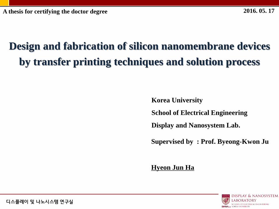
Table of Contents
Introduction
Silicon Nanomembrane Transfer with Suspended Configurations
Self-assembly of Au Nanoparticles Arrays and Transfer
Application devices
Conclusion
I
II
III
IV
IIV
▪1) Flexible low-voltage pentacene memory with Au nanoparticles
▪2) Multifunction Silicon Nanomembrane Schottky Diodes Based on Au Nanoparticles
▪3) A Zero Capacitance RAM with Solution Doping Process
- 3/38 - 디스플레이 및 나노시스템 연구실
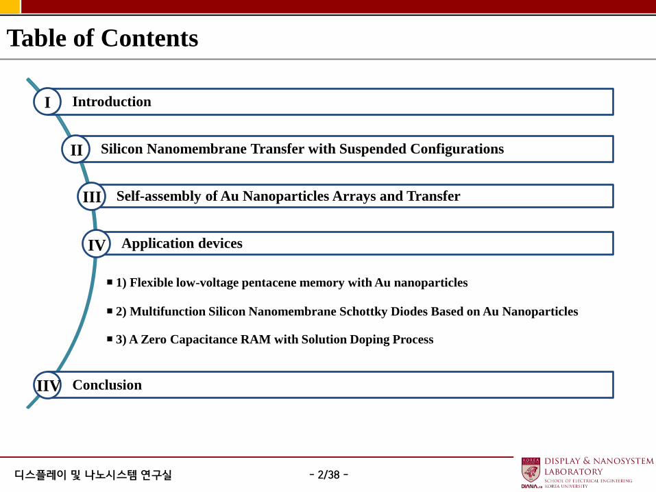
Table of Contents
Introduction
Silicon Nanomembrane Transfer with Suspended Configurations
Self-assembly of Au Nanoparticles Arrays and Transfer
Application devices
Conclusion
I
II
III
IV
IIV
▪1) Flexible low-voltage pentacene memory with Au nanoparticles
▪2) Multifunction Silicon Nanomembrane Schottky Diodes Based on Au Nanoparticles
▪3) A Zero Capacitance RAM with Solution Doping Process
- 4/38 - 디스플레이 및 나노시스템 연구실
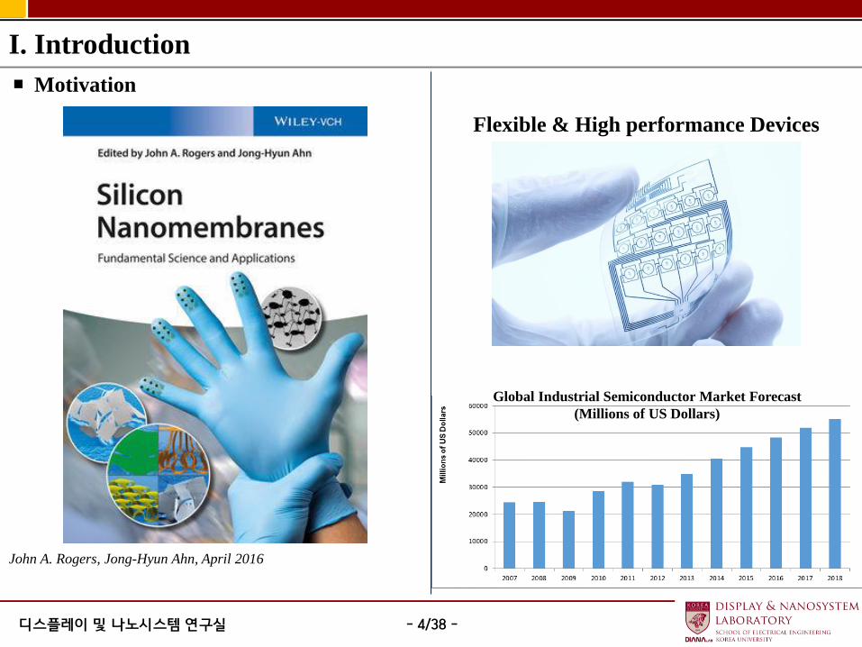
I. Introduction
▪ Motivation
John A. Rogers, Jong-Hyun Ahn, April 2016
Flexible & High performance Devices
Global Industrial Semiconductor Market Forecast
(Millions of US Dollars)
- 5/38 - 디스플레이 및 나노시스템 연구실
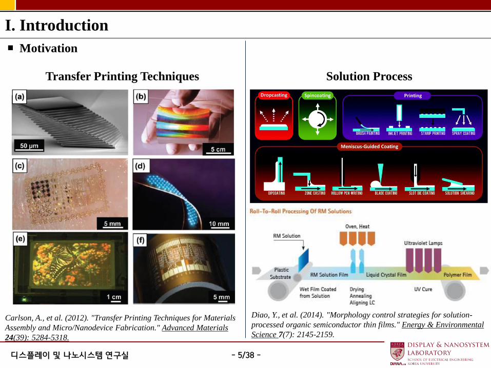
I. Introduction
Solution Process Transfer Printing Techniques
▪ Motivation
Carlson, A., et al. (2012). "Transfer Printing Techniques for Materials
Assembly and Micro/Nanodevice Fabrication." Advanced Materials
24(39): 5284-5318.
Diao, Y., et al. (2014). "Morphology control strategies for solution-
processed organic semiconductor thin films." Energy & Environmental
Science 7(7): 2145-2159.
- 6/38 - 디스플레이 및 나노시스템 연구실
Table of Contents
Introduction
Silicon Nanomembrane Transfer with Suspended Configurations
Self-assembly of Au Nanoparticles Arrays and Transfer
Application devices
Conclusion
I
II
III
IV
IIV
▪1) Flexible low-voltage pentacene memory with Au nanoparticles
▪2) Multifunction Silicon Nanomembrane Schottky Diodes Based on Au Nanoparticles
▪3) A Zero Capacitance RAM with Solution Doping Process
- 7/38 - 디스플레이 및 나노시스템 연구실
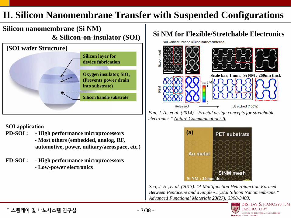
II. Silicon Nanomembrane Transfer with Suspended Configurations
Silicon nanomembrane (Si NM)
& Silicon-on-insulator (SOI)
Silicon layer for
device fabrication
[SOI wafer Structure]
Oxygen insulator, SiO2
(Prevents power drain
into substrate)
Silicon handle substrate
SOI application
PD-SOI : - High performance microprocessors
- Most others (embedded, analog, RF,
automotive, power, military/aerospace, etc.)
FD-SOI : - High performance microprocessors
- Low-power electronics
Si NM for Flexible/Stretchable Electronics
Seo, J. H., et al. (2013). "A Multifunction Heterojunction Formed
Between Pentacene and a Single-Crystal Silicon Nanomembrane."
Advanced Functional Materials 23(27): 3398-3403.
Fan, J. A., et al. (2014). "Fractal design concepts for stretchable
electronics." Nature Communications 5.
Scale bar, 1 mm. Si NM : 260nm thick
Si NM : 340nm thick
- 8/38 - 디스플레이 및 나노시스템 연구실
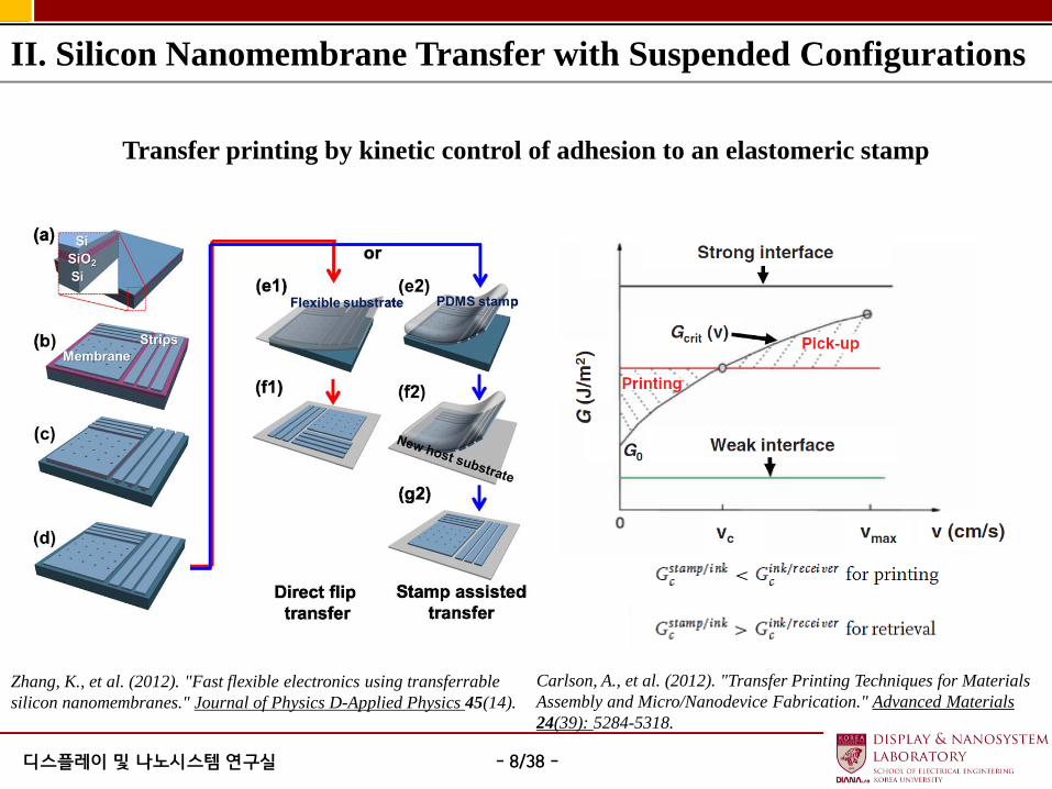
II. Silicon Nanomembrane Transfer with Suspended Configurations
Transfer printing by kinetic control of adhesion to an elastomeric stamp
Zhang, K., et al. (2012). "Fast flexible electronics using transferrable
silicon nanomembranes." Journal of Physics D-Applied Physics 45(14).
Carlson, A., et al. (2012). "Transfer Printing Techniques for Materials
Assembly and Micro/Nanodevice Fabrication." Advanced Materials
24(39): 5284-5318.
- 9/38 - 디스플레이 및 나노시스템 연구실
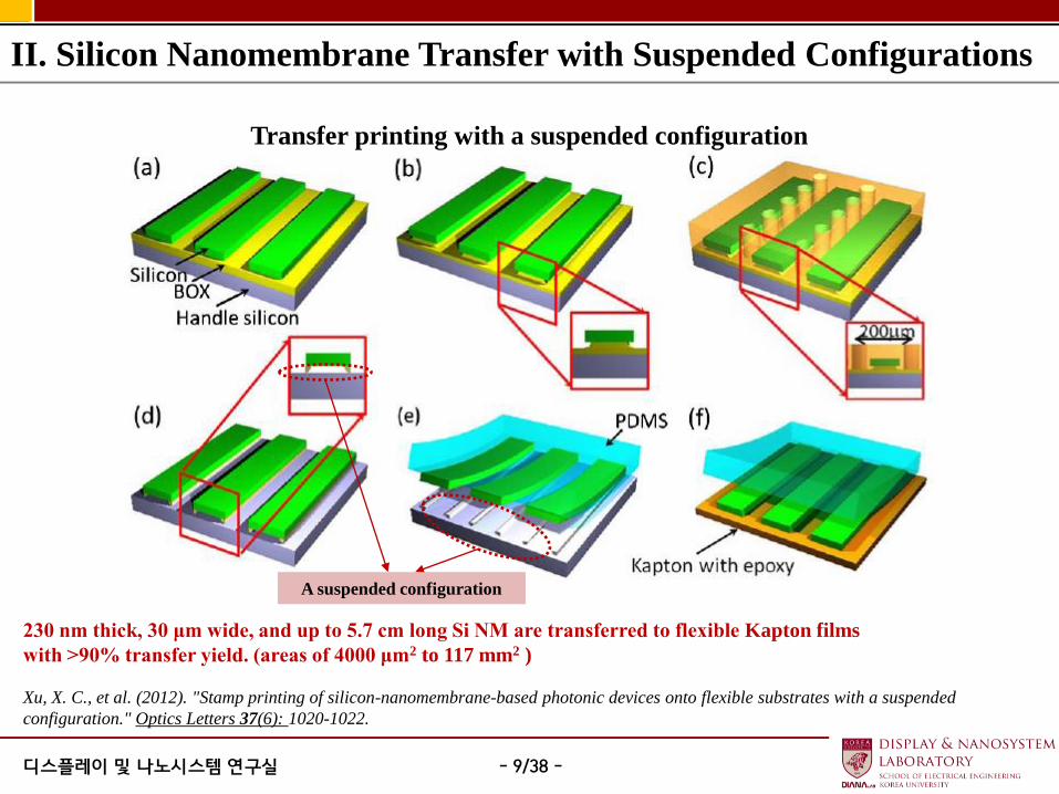
II. Silicon Nanomembrane Transfer with Suspended Configurations
Xu, X. C., et al. (2012). "Stamp printing of silicon-nanomembrane-based photonic devices onto flexible substrates with a suspended
configuration." Optics Letters 37(6): 1020-1022.
230 nm thick, 30 μm wide, and up to 5.7 cm long Si NM are transferred to flexible Kapton films
with >90% transfer yield. (areas of 4000 μm2 to 117 mm2 )
A suspended configuration
Transfer printing with a suspended configuration
- 10/38 - 디스플레이 및 나노시스템 연구실
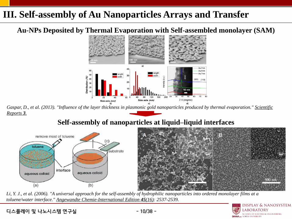
III. Self-assembly of Au Nanoparticles Arrays and Transfer
Au-NPs Deposited by Thermal Evaporation with Self-assembled monolayer (SAM)
Self-assembly of nanoparticles at liquid–liquid interfaces
Li, Y. J., et al. (2006). "A universal approach for the self-assembly of hydrophilic nanoparticles into ordered monolayer films at a
toluene/water interface." Angewandte Chemie-International Edition 45(16): 2537-2539.
Gaspar, D., et al. (2013). "Influence of the layer thickness in plasmonic gold nanoparticles produced by thermal evaporation." Scientific
Reports 3.
- 11/38 - 디스플레이 및 나노시스템 연구실
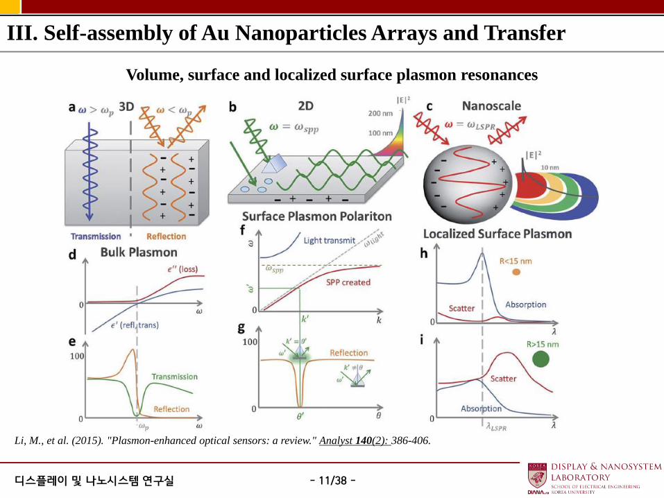
III. Self-assembly of Au Nanoparticles Arrays and Transfer
Volume, surface and localized surface plasmon resonances
Li, M., et al. (2015). "Plasmon-enhanced optical sensors: a review." Analyst 140(2): 386-406.
- 12/38 - 디스플레이 및 나노시스템 연구실
Table of Contents
Introduction
Silicon Nanomembrane Transfer with Suspended Configurations
Self-assembly of Au Nanoparticles Arrays and Transfer
Application devices
Conclusion
I
II
III
IV
IIV
▪1) Flexible low-voltage pentacene memory with Au nanoparticles
▪2) Multifunction Silicon Nanomembrane Schottky Diodes Based on Au Nanoparticles
▪3) A Zero Capacitance RAM with Solution Doping Process
- 13/38 - 디스플레이 및 나노시스템 연구실
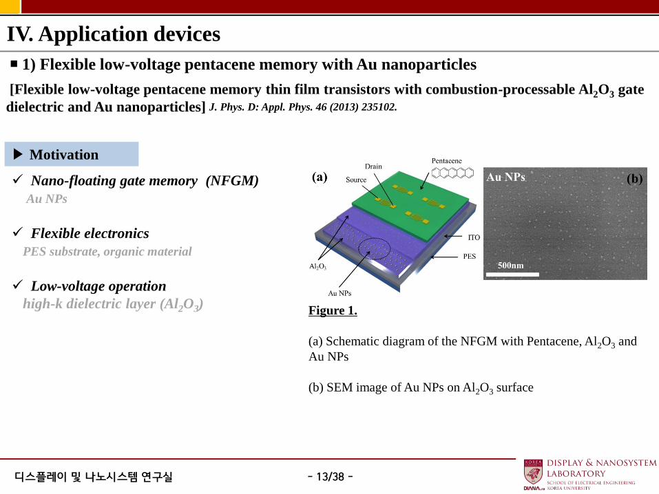
IV. Application devices
▪1) Flexible low-voltage pentacene memory with Au nanoparticles
▶ Motivation
J. Phys. D: Appl. Phys. 46 (2013) 235102.
Figure 1.
(a) Schematic diagram of the NFGM with Pentacene, Al2O3 and
Au NPs
(b) SEM image of Au NPs on Al2O3 surface
Nano-floating gate memory (NFGM)
Au NPs
Flexible electronics
PES substrate, organic material
Low-voltage operation
high-k dielectric layer (Al2O3)
[Flexible low-voltage pentacene memory thin film transistors with combustion-processable Al2O3 gate
dielectric and Au nanoparticles]
- 14/38 - 디스플레이 및 나노시스템 연구실
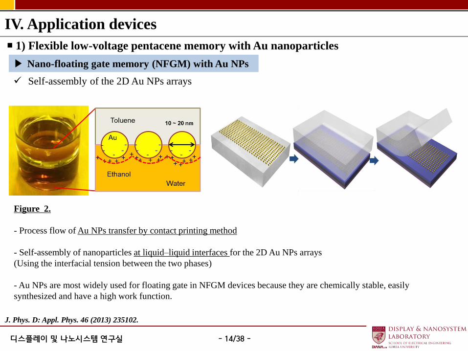
IV. Application devices
▪1) Flexible low-voltage pentacene memory with Au nanoparticles
J. Phys. D: Appl. Phys. 46 (2013) 235102.
Figure 2.
- Process flow of Au NPs transfer by contact printing method
- Self-assembly of nanoparticles at liquid–liquid interfaces for the 2D Au NPs arrays
(Using the interfacial tension between the two phases)
- Au NPs are most widely used for floating gate in NFGM devices because they are chemically stable, easily
synthesized and have a high work function.
▶ Nano-floating gate memory (NFGM) with Au NPs
Self-assembly of the 2D Au NPs arrays
- 15/38 - 디스플레이 및 나노시스템 연구실
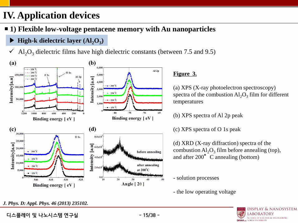
IV. Application devices
▪1) Flexible low-voltage pentacene memory with Au nanoparticles
J. Phys. D: Appl. Phys. 46 (2013) 235102.
Figure 3.
(a) XPS (X-ray photoelectron spectroscopy)
spectra of the combustion Al2O3 film for different
temperatures
(b) XPS spectra of Al 2p peak
(c) XPS spectra of O 1s peak
(d) XRD (X-ray diffraction) spectra of the
combustion Al2O3 film before annealing (top),
and after 200°C annealing (bottom)
- solution processes
- the low operating voltage
▶ High-k dielectric layer (Al2O3)
Al2O3 dielectric films have high dielectric constants (between 7.5 and 9.5)
- 16/38 - 디스플레이 및 나노시스템 연구실
IV. Application devices
▪1) Flexible low-voltage pentacene memory with Au nanoparticles
J. Phys. D: Appl. Phys. 46 (2013) 235102.
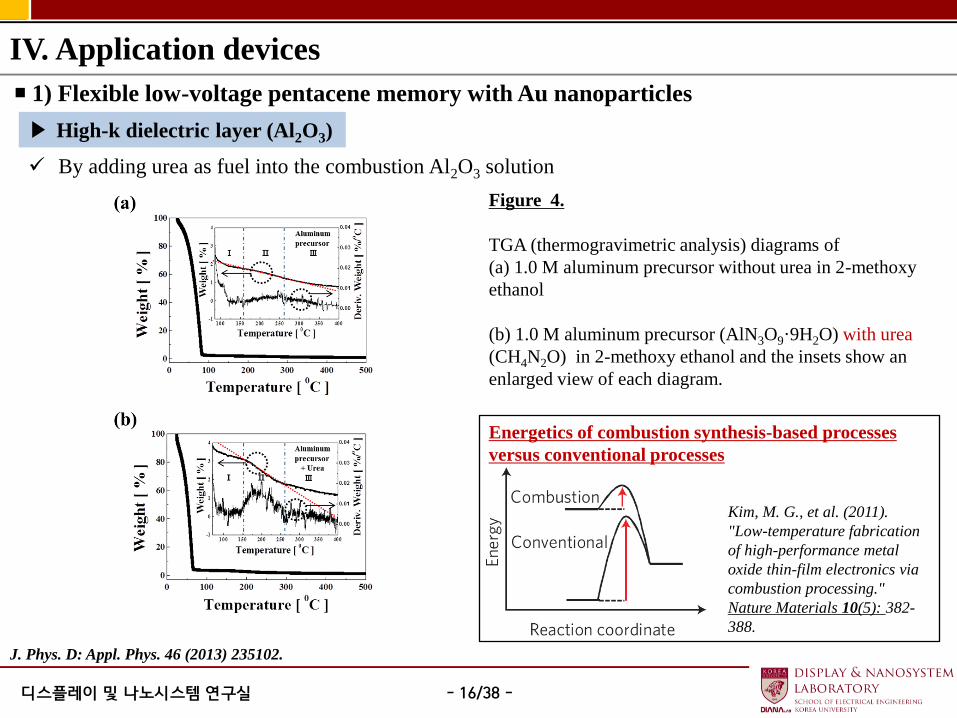
Figure 4.
TGA (thermogravimetric analysis) diagrams of
(a) 1.0 M aluminum precursor without urea in 2-methoxy
ethanol
(b) 1.0 M aluminum precursor (AlN3O9·9H2O) with urea
(CH4N2O) in 2-methoxy ethanol and the insets show an
enlarged view of each diagram.
▶ High-k dielectric layer (Al2O3)
By adding urea as fuel into the combustion Al2O3 solution
Energetics of combustion synthesis-based processes
versus conventional processes
Kim, M. G., et al. (2011).
"Low-temperature fabrication
of high-performance metal
oxide thin-film electronics via
combustion processing."
Nature Materials 10(5): 382-
388.
- 17/38 - 디스플레이 및 나노시스템 연구실
IV. Application devices
▪1) Flexible low-voltage pentacene memory with Au nanoparticles
J. Phys. D: Appl. Phys. 46 (2013) 235102.
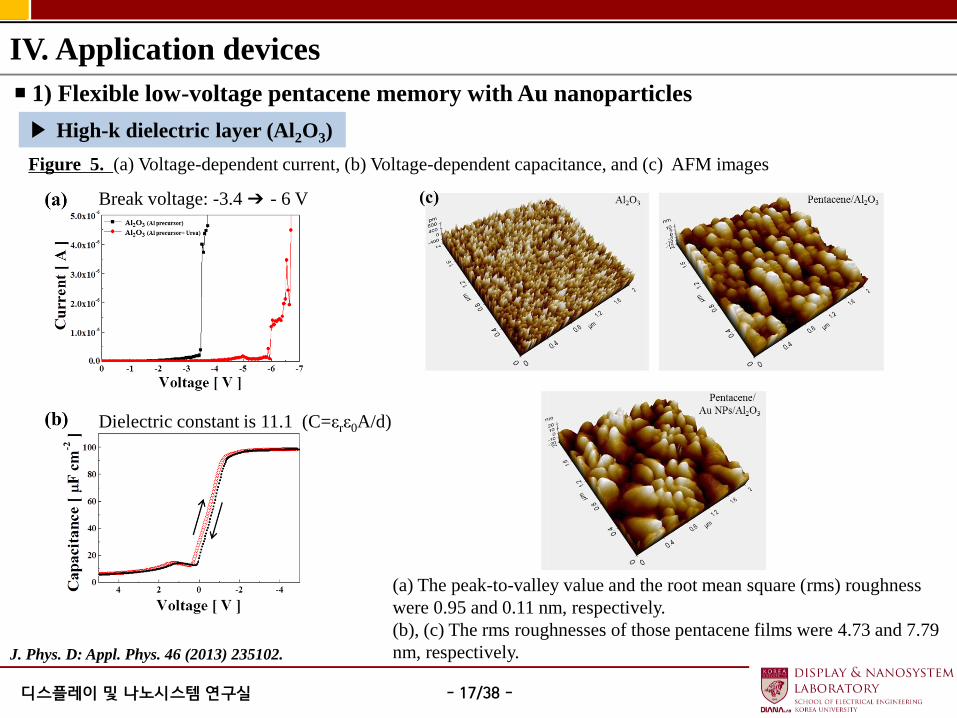
Figure 5. (a) Voltage-dependent current, (b) Voltage-dependent capacitance, and (c) AFM images
▶ High-k dielectric layer (Al2O3)
Dielectric constant is 11.1 (C=εrε0A/d)
Break voltage: -3.4 ➔ - 6 V
(a) The peak-to-valley value and the root mean square (rms) roughness
were 0.95 and 0.11 nm, respectively.
(b), (c) The rms roughnesses of those pentacene films were 4.73 and 7.79
nm, respectively.
- 18/38 - 디스플레이 및 나노시스템 연구실
IV. Application devices
▪1) Flexible low-voltage pentacene memory with Au nanoparticles
J. Phys. D: Appl. Phys. 46 (2013) 235102.
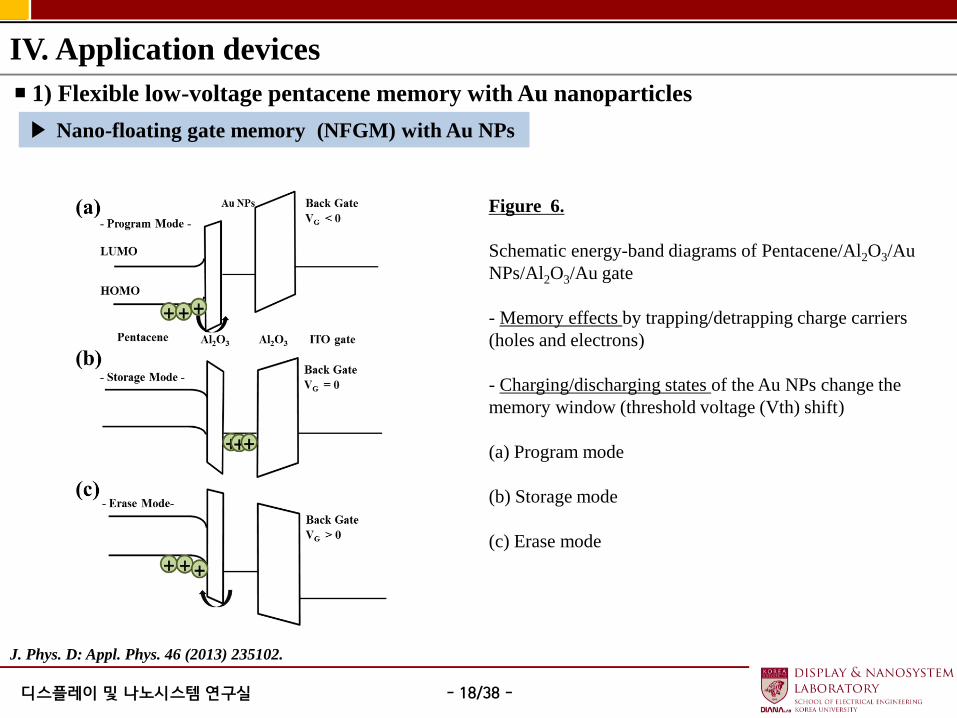
▶ Nano-floating gate memory (NFGM) with Au NPs
Figure 6.
Schematic energy-band diagrams of Pentacene/Al2O3/Au
NPs/Al2O3/Au gate
- Memory effects by trapping/detrapping charge carriers
(holes and electrons)
- Charging/discharging states of the Au NPs change the
memory window (threshold voltage (Vth) shift)
(a) Program mode
(b) Storage mode
(c) Erase mode
- 19/38 - 디스플레이 및 나노시스템 연구실
IV. Application devices
▪1) Flexible low-voltage pentacene memory with Au nanoparticles
J. Phys. D: Appl. Phys. 46 (2013) 235102.
▶ Nano-floating gate memory (NFGM) with Au NPs
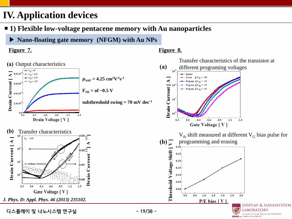
Figure 7. Figure 8.
Transfer characteristics of the transistor at
different programing voltages
Vth shift measured at different VG bias pulse for
programming and erasing
Output characteristics
Transfer characteristics
𝝁𝒔𝒂𝒕 = 4.25 cm2V-1s-1
𝑽𝒕𝒉 = of ~0.5 V
subthreshold swing = 70 mV dec-1
- 20/38 - 디스플레이 및 나노시스템 연구실
IV. Application devices
▪2) Multifunction Silicon Nanomembrane Schottky Diodes Based on Au Nanoparticles
▶ Motivation
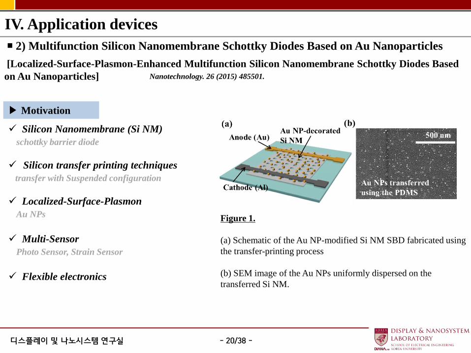
Figure 1.
(a) Schematic of the Au NP-modified Si NM SBD fabricated using
the transfer-printing process
(b) SEM image of the Au NPs uniformly dispersed on the
transferred Si NM.
Silicon Nanomembrane (Si NM)
schottky barrier diode
Silicon transfer printing techniques
transfer with Suspended configuration
Localized-Surface-Plasmon
Au NPs
Multi-Sensor
Photo Sensor, Strain Sensor
Flexible electronics
[Localized-Surface-Plasmon-Enhanced Multifunction Silicon Nanomembrane Schottky Diodes Based
on Au Nanoparticles] Nanotechnology. 26 (2015) 485501.
- 21/38 - 디스플레이 및 나노시스템 연구실
IV. Application devices
▪2) Multifunction Silicon Nanomembrane Schottky Diodes Based on Au Nanoparticles
Nanotechnology. 26 (2015) 485501.
▶ Silicon transfer printing techniques
Transfer printing with a suspended configuration (i.e., pedestals)
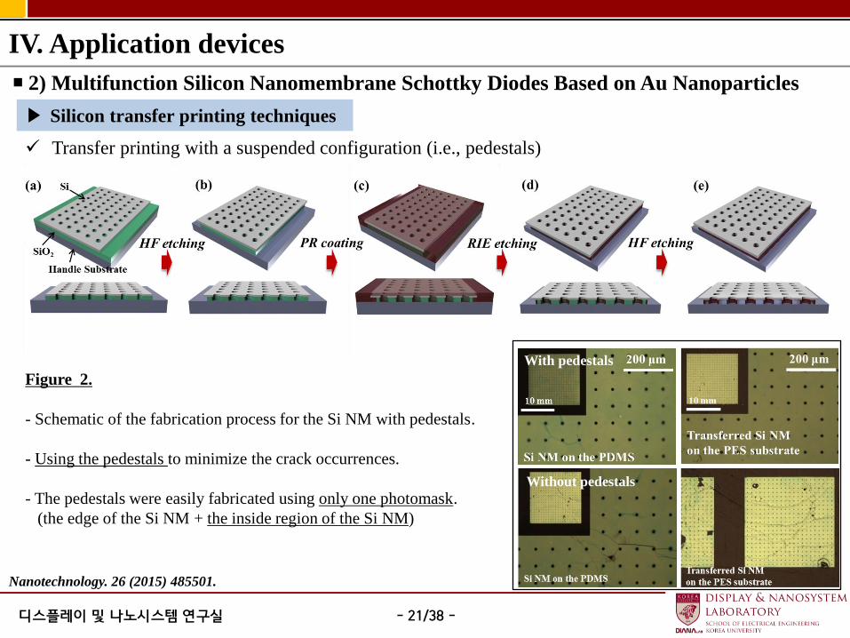
Figure 2.
- Schematic of the fabrication process for the Si NM with pedestals.
- Using the pedestals to minimize the crack occurrences.
- The pedestals were easily fabricated using only one photomask.
(the edge of the Si NM + the inside region of the Si NM)
With pedestals
Without pedestals
- 22/38 - 디스플레이 및 나노시스템 연구실
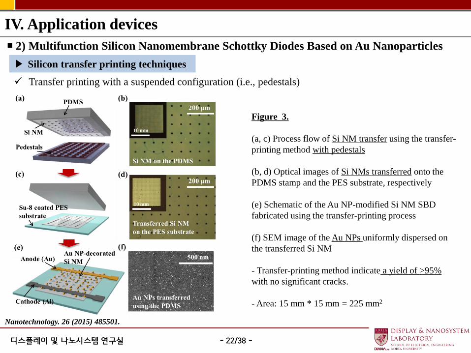
Figure 3.
(a, c) Process flow of Si NM transfer using the transfer-
printing method with pedestals
(b, d) Optical images of Si NMs transferred onto the
PDMS stamp and the PES substrate, respectively
(e) Schematic of the Au NP-modified Si NM SBD
fabricated using the transfer-printing process
(f) SEM image of the Au NPs uniformly dispersed on
the transferred Si NM
- Transfer-printing method indicate a yield of >95%
with no significant cracks.
- Area: 15 mm * 15 mm = 225 mm2
IV. Application devices
▪2) Multifunction Silicon Nanomembrane Schottky Diodes Based on Au Nanoparticles
Nanotechnology. 26 (2015) 485501.
▶ Silicon transfer printing techniques
Transfer printing with a suspended configuration (i.e., pedestals)
- 23/38 - 디스플레이 및 나노시스템 연구실
IV. Application devices
▪2) Multifunction Silicon Nanomembrane Schottky Diodes Based on Au Nanoparticles
Nanotechnology. 26 (2015) 485501.
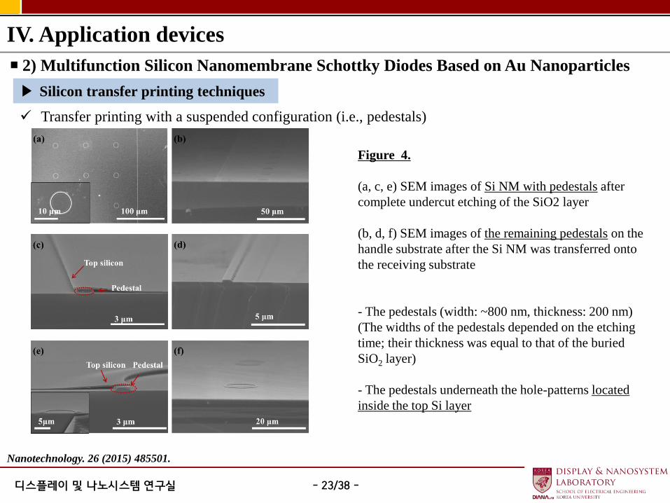
Figure 4.
(a, c, e) SEM images of Si NM with pedestals after
complete undercut etching of the SiO2 layer
(b, d, f) SEM images of the remaining pedestals on the
handle substrate after the Si NM was transferred onto
the receiving substrate
- The pedestals (width: ~800 nm, thickness: 200 nm)
(The widths of the pedestals depended on the etching
time; their thickness was equal to that of the buried
SiO2 layer)
- The pedestals underneath the hole-patterns located
inside the top Si layer
▶ Silicon transfer printing techniques
Transfer printing with a suspended configuration (i.e., pedestals)
- 24/38 - 디스플레이 및 나노시스템 연구실
IV. Application devices
▪2) Multifunction Silicon Nanomembrane Schottky Diodes Based on Au Nanoparticles
Nanotechnology. 26 (2015) 485501.
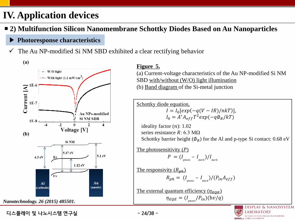
Figure 5.
(a) Current-voltage characteristics of the Au NP-modified Si NM
SBD with/without (W/O) light illumination
(b) Band diagram of the Si-metal junction
▶ Photoresponse characteristics
The Au NP-modified Si NM SBD exhibited a clear rectifying behavior
Schottky diode equation,
𝐼 = 𝐼0[𝑒𝑥𝑝 −𝑞(𝑉 − 𝐼𝑅)/𝑛𝑘𝑇 ], 𝐼0 = 𝐴∗𝐴𝑒𝑓𝑓𝑇2𝑒𝑥𝑝(−𝑞∅𝐵/𝑘𝑇)
The photosensitivity (𝑃)
𝑃 = (𝐼𝑝ℎ𝑜𝑡𝑜
– 𝐼𝑑𝑎𝑟𝑘
)/𝐼𝑑𝑎𝑟𝑘
The responsivity (𝑅𝑝ℎ)
𝑅𝑝ℎ = (𝐼𝑝ℎ𝑜𝑡𝑜
– 𝐼𝑑𝑎𝑟𝑘
)/(𝑃𝑖𝑛𝐴𝑒𝑓𝑓)
The external quantum efficiency (𝜂𝐸𝑄𝐸)
𝜂𝐸𝑄𝐸 = (𝐼𝑝ℎ𝑜𝑡𝑜
/𝑃𝑖𝑛)(h𝑣/𝑞)
ideality factor (𝑛): 1.02
series resistance 𝑅: 6.3 MΩ
Schottky barrier height (∅𝐵) for the Al and p-type Si contact: 0.68 eV
- 25/38 - 디스플레이 및 나노시스템 연구실
IV. Application devices
▪2) Multifunction Silicon Nanomembrane Schottky Diodes Based on Au Nanoparticles
Nanotechnology. 26 (2015) 485501.
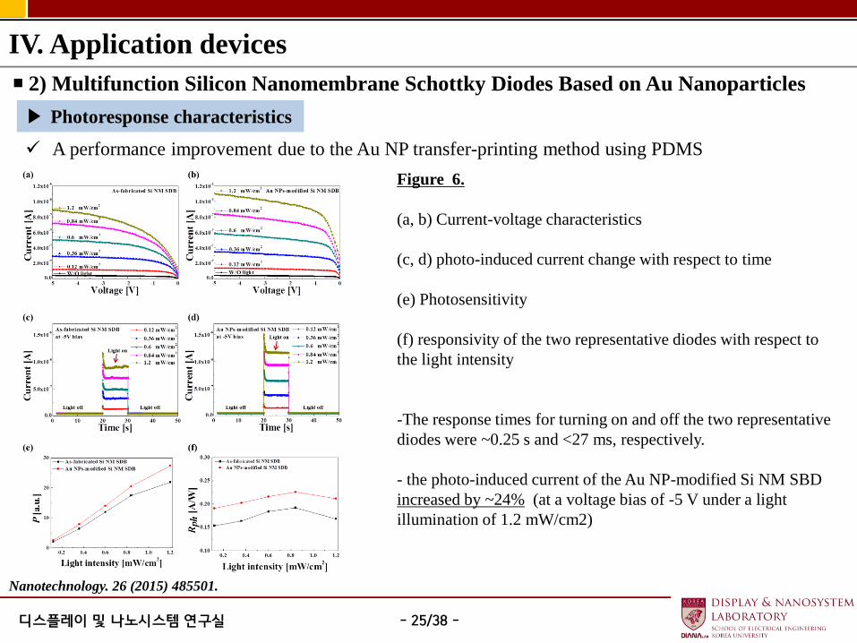
Figure 6.
(a, b) Current-voltage characteristics
(c, d) photo-induced current change with respect to time
(e) Photosensitivity
(f) responsivity of the two representative diodes with respect to
the light intensity
-The response times for turning on and off the two representative
diodes were ~0.25 s and <27 ms, respectively.
- the photo-induced current of the Au NP-modified Si NM SBD
increased by ~24% (at a voltage bias of -5 V under a light
illumination of 1.2 mW/cm2)
▶ Photoresponse characteristics
A performance improvement due to the Au NP transfer-printing method using PDMS
- 26/38 - 디스플레이 및 나노시스템 연구실
IV. Application devices
▪2) Multifunction Silicon Nanomembrane Schottky Diodes Based on Au Nanoparticles
Nanotechnology. 26 (2015) 485501.
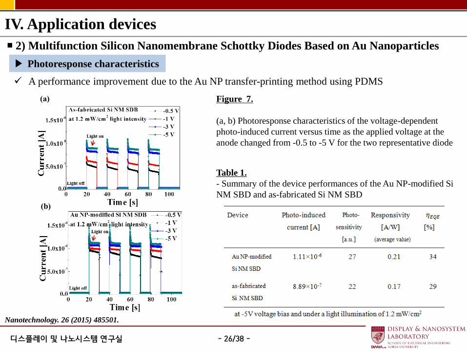
Figure 7.
(a, b) Photoresponse characteristics of the voltage-dependent
photo-induced current versus time as the applied voltage at the
anode changed from -0.5 to -5 V for the two representative diode
▶ Photoresponse characteristics
A performance improvement due to the Au NP transfer-printing method using PDMS
Table 1.
- Summary of the device performances of the Au NP-modified Si
NM SBD and as-fabricated Si NM SBD
- 27/38 - 디스플레이 및 나노시스템 연구실
IV. Application devices
▪2) Multifunction Silicon Nanomembrane Schottky Diodes Based on Au Nanoparticles
Nanotechnology. 26 (2015) 485501.
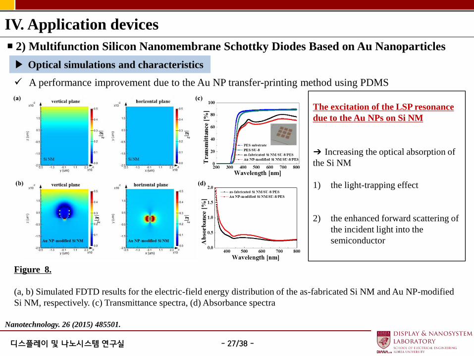
Figure 8.
(a, b) Simulated FDTD results for the electric-field energy distribution of the as-fabricated Si NM and Au NP-modified
Si NM, respectively. (c) Transmittance spectra, (d) Absorbance spectra
▶ Optical simulations and characteristics
A performance improvement due to the Au NP transfer-printing method using PDMS
The excitation of the LSP resonance
due to the Au NPs on Si NM
➔ Increasing the optical absorption of
the Si NM
1) the light-trapping effect
2) the enhanced forward scattering of
the incident light into the
semiconductor
- 28/38 - 디스플레이 및 나노시스템 연구실
IV. Application devices
▪2) Multifunction Silicon Nanomembrane Schottky Diodes Based on Au Nanoparticles
Nanotechnology. 26 (2015) 485501.
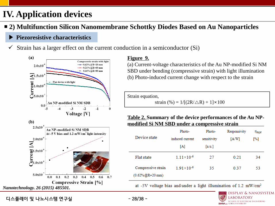
Figure 9.
(a) Current-voltage characteristics of the Au NP-modified Si NM
SBD under bending (compressive strain) with light illumination
(b) Photo-induced current change with respect to the strain
▶ Piezoresistive characteristics
Strain has a larger effect on the current conduction in a semiconductor (Si)
Table 2. Summary of the device performances of the Au NP-
modified Si NM SBD under a compressive strain
Strain equation,
strain (%) = 1/[(2R/△R) + 1]×100
- 29/38 - 디스플레이 및 나노시스템 연구실
IV. Application devices
▪3) A Zero Capacitance RAM with Solution Doping Process
▶ Motivation
(To be submitted)
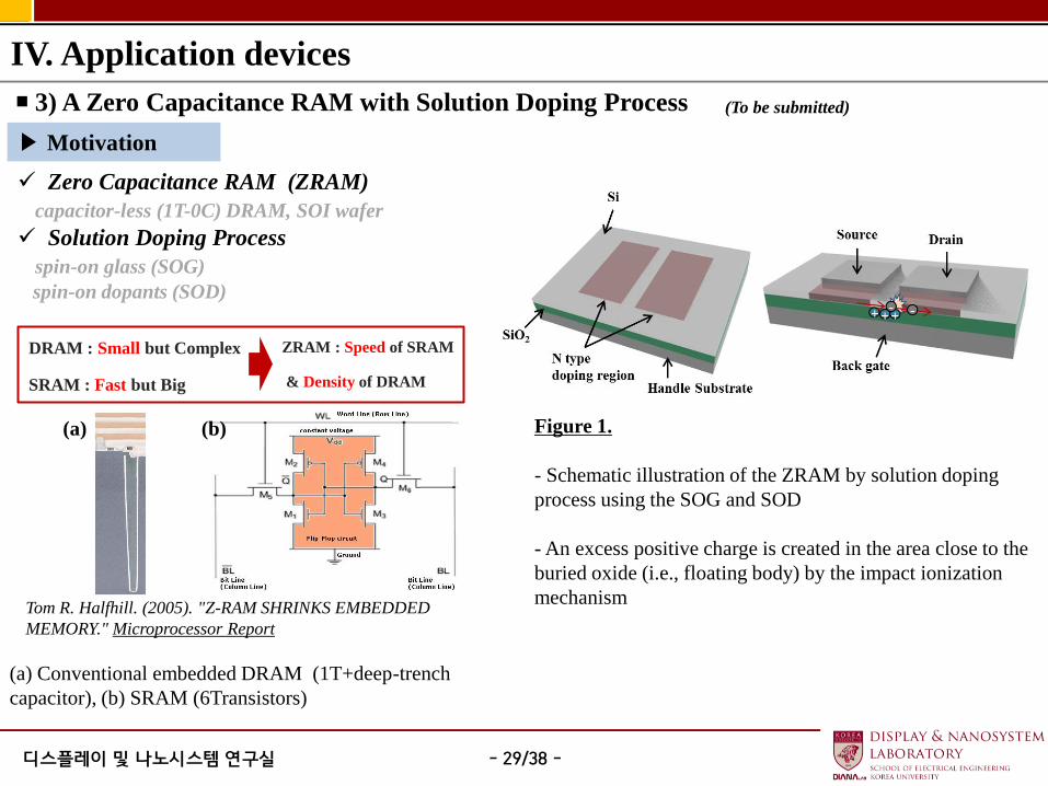
Figure 1.
- Schematic illustration of the ZRAM by solution doping
process using the SOG and SOD
- An excess positive charge is created in the area close to the
buried oxide (i.e., floating body) by the impact ionization
mechanism
Zero Capacitance RAM (ZRAM)
capacitor-less (1T-0C) DRAM, SOI wafer
Solution Doping Process
spin-on glass (SOG)
spin-on dopants (SOD)
(a) Conventional embedded DRAM (1T+deep-trench
capacitor), (b) SRAM (6Transistors)
(a) (b)
Tom R. Halfhill. (2005). "Z-RAM SHRINKS EMBEDDED
MEMORY." Microprocessor Report
DRAM : Small but Complex
SRAM : Fast but Big
ZRAM : Speed of SRAM
& Density of DRAM
- 30/38 - 디스플레이 및 나노시스템 연구실
IV. Application devices
▪3) A Zero Capacitance RAM with Solution Doping Process
▶ Motivation (ZRAM)
- 31/38 - 디스플레이 및 나노시스템 연구실
IV. Application devices
▪3) A Zero Capacitance RAM with Solution Doping Process
(To be submitted)
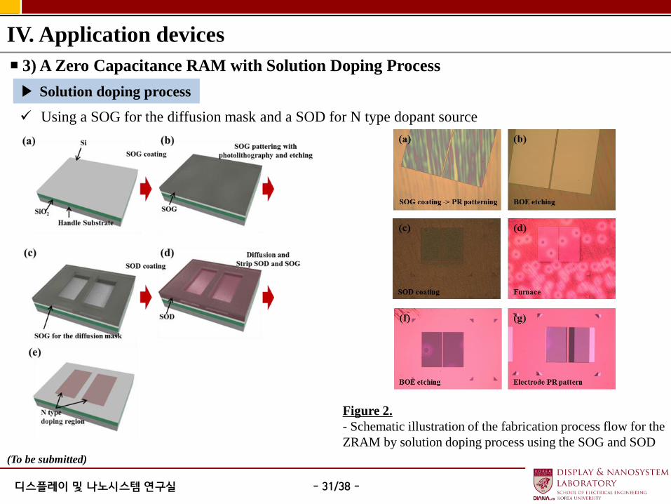
▶ Solution doping process
Using a SOG for the diffusion mask and a SOD for N type dopant source
Figure 2.
- Schematic illustration of the fabrication process flow for the
ZRAM by solution doping process using the SOG and SOD
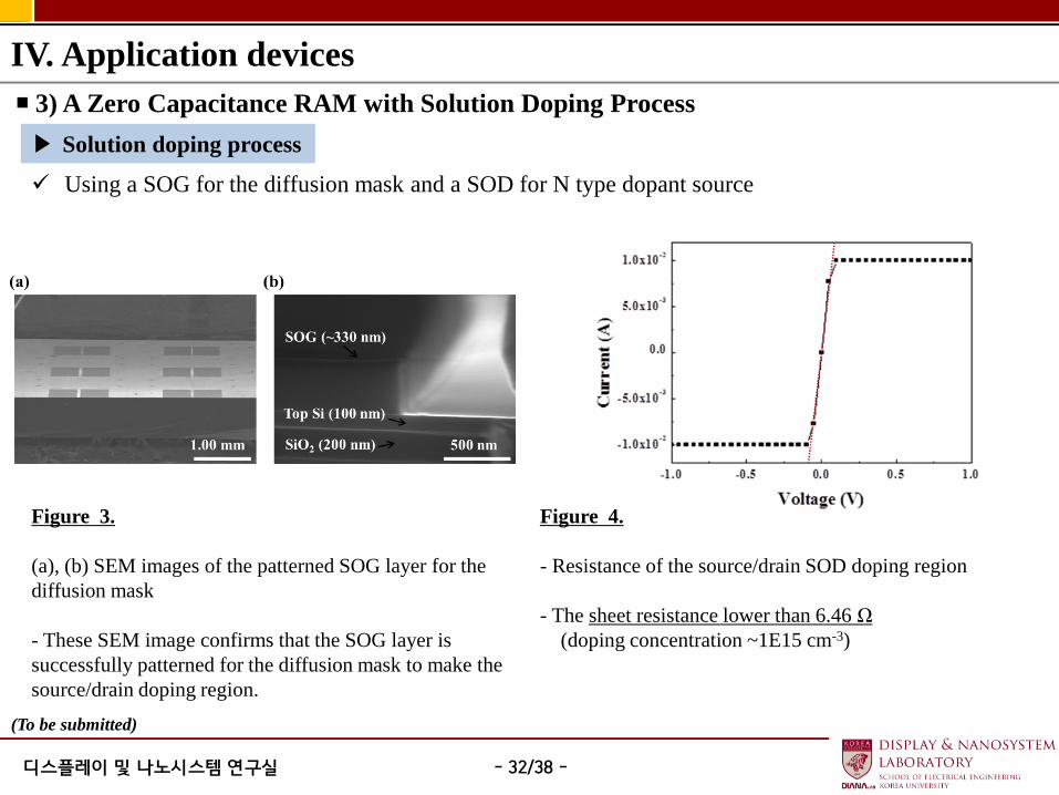
- 32/38 - 디스플레이 및 나노시스템 연구실
Figure 4.
- Resistance of the source/drain SOD doping region
- The sheet resistance lower than 6.46 Ω
(doping concentration ~1E15 cm-3)
IV. Application devices
▪3) A Zero Capacitance RAM with Solution Doping Process
(To be submitted)
▶ Solution doping process
Using a SOG for the diffusion mask and a SOD for N type dopant source
Figure 3.
(a), (b) SEM images of the patterned SOG layer for the
diffusion mask
- These SEM image confirms that the SOG layer is
successfully patterned for the diffusion mask to make the
source/drain doping region.
- 33/38 - 디스플레이 및 나노시스템 연구실
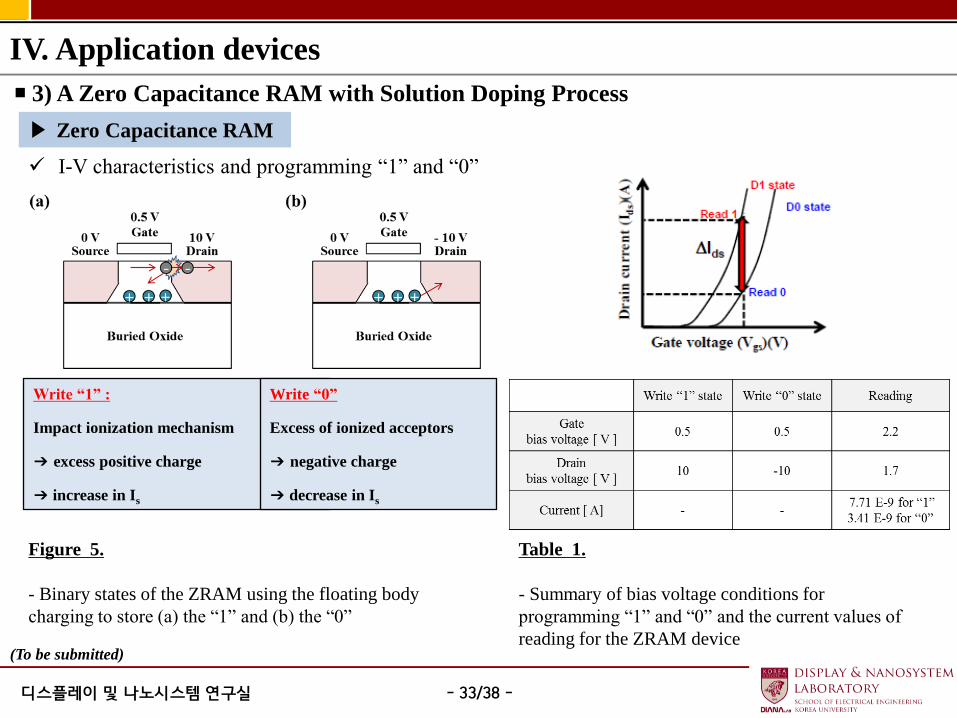
Table 1.
- Summary of bias voltage conditions for
programming “1” and “0” and the current values of
reading for the ZRAM device
IV. Application devices
▪3) A Zero Capacitance RAM with Solution Doping Process
(To be submitted)
▶ Zero Capacitance RAM
I-V characteristics and programming “1” and “0”
Figure 5.
- Binary states of the ZRAM using the floating body
charging to store (a) the “1” and (b) the “0”
Write “1” :
Impact ionization mechanism
➔ excess positive charge
➔ increase in Is
Write “0”
Excess of ionized acceptors
➔ negative charge
➔ decrease in Is
- 34/38 - 디스플레이 및 나노시스템 연구실
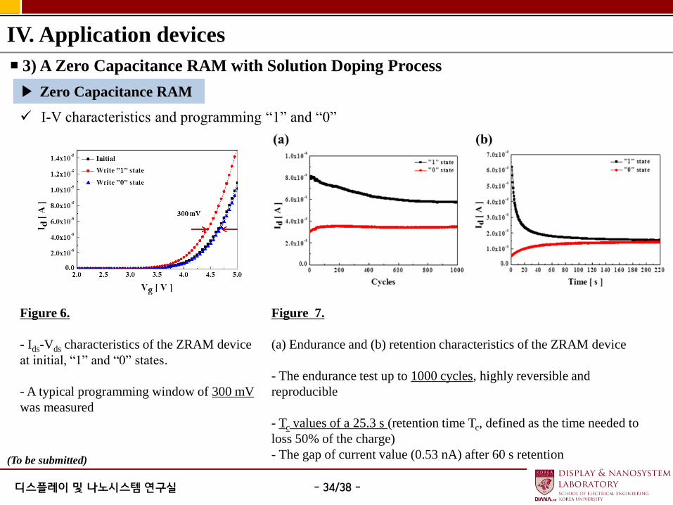
Figure 7.
(a) Endurance and (b) retention characteristics of the ZRAM device
- The endurance test up to 1000 cycles, highly reversible and
reproducible
- Tc values of a 25.3 s (retention time Tc, defined as the time needed to
loss 50% of the charge)
- The gap of current value (0.53 nA) after 60 s retention
IV. Application devices
▪3) A Zero Capacitance RAM with Solution Doping Process
(To be submitted)
▶ Zero Capacitance RAM
I-V characteristics and programming “1” and “0”
Figure 6.
- Ids-Vds characteristics of the ZRAM device
at initial, “1” and “0” states.
- A typical programming window of 300 mV
was measured
- 35/38 - 디스플레이 및 나노시스템 연구실
Table of Contents
Introduction
Silicon Nanomembrane Transfer with Suspended Configurations
Self-assembly of Au Nanoparticles Arrays and Transfer
Application devices
Conclusion
I
II
III
IV
IIV
▪1) Flexible low-voltage pentacene memory with Au nanoparticles
▪2) Multifunction Silicon Nanomembrane Schottky Diodes Based on Au Nanoparticles
▪3) A Zero Capacitance RAM with Solution Doping Process
- 36/38 - 디스플레이 및 나노시스템 연구실
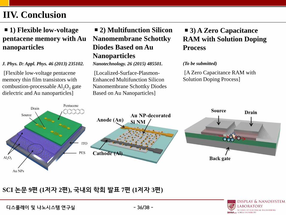
IIV. Conclusion
▪3) A Zero Capacitance
RAM with Solution Doping
Process
▪1) Flexible low-voltage
pentacene memory with Au
nanoparticles
▪2) Multifunction Silicon
Nanomembrane Schottky
Diodes Based on Au
Nanoparticles
SCI 논문 9편 (1저자 2편), 국내외 학회 발표 7편 (1저자 3편)
J. Phys. D: Appl. Phys. 46 (2013) 235102. Nanotechnology. 26 (2015) 485501. (To be submitted)
[Flexible low-voltage pentacene
memory thin film transistors with
combustion-processable Al2O3 gate
dielectric and Au nanoparticles]
[Localized-Surface-Plasmon-
Enhanced Multifunction Silicon
Nanomembrane Schottky Diodes
Based on Au Nanoparticles]
[A Zero Capacitance RAM with
Solution Doping Process]

- 37/38 - 디스플레이 및 나노시스템 연구실
경청해 주셔서 감사합니다.
- 38/38 - 디스플레이 및 나노시스템 연구실
Appendix
[1] “The electrical and photoconductivity characteristics of donor-acceptor alternating copolymer using solution process,” Shin Woo Jeong, Gi
Back Lee, Hyeon-Jun Ha, Soon-Ki Kwon, Yun-Hi Kim, and Byeong Kwon Ju, Applied Physics Letters, 101, 243301 (2012)
[2] “The silicon Schottky diode on flexible substrates by transfer method.” Tae-Yeon Oh, Shin Woo Jeong, Seongpil Chang, Kookhyun Choi,
Hyun Jun Ha, and Byeong Kwon Ju, Applied Physics Letters, 102, 021106 (2013)
[3] “Post Annealing Effects on the Electrical Characteristics of Pentacene Thin Film Transistors on Flexible Substrates,” Tae-Yeon Oh, Shin
Woo Jeong, Seongpil Chang, Jung-Ho Park, Jong-Woo Kim, Kookhyun Choi, Hyeon-Jun Ha, Bo-Yeon Hwang, and Byeong-Kwon Ju,
Journal of Nanoscience and Nanotechnology, 13 5, pp. 3491-3494(4) (2013)
[4] “Flexible low-voltage pentacene memory thin-film transistors with combustion-processable Al2O3 gate,” Hyeon Jun Ha, ShinWoo Jeong,
Tae-Yeon Oh, Minseok Kim, Kookhyun Choi, Jung Ho Park, and Byeong-Kwon Ju, J. Phys. D: Appl. Phys, 46, 235102 (2013)
[5] “Flexible organic phototransistors based on a combination of printing methods,” Minseok Kim, Hyun-Jun Ha, Hui-Jun Yun, In-Kyu You,
Kang-Jun Baeg, Yun-Hi Kim, and Byeong-Kwon Ju, Organic Electronics, 15, pp. 2677–2684 (2014)
[6] “Highly flexible titanium dioxide-based resistive switching memory with simple fabrication,” Seung-Won Yeom, Suk Won Park, In-sung
Jung, Minseok Kim, Hyeon Jun Ha, Joon Hyung Shim, and Byeong-Kwon Ju, Applied Physics Express, 7, 101801 (2014)
[7] “Localized-surface-plasmon-enhanced multifunction silicon nanomembrane Schottky diodes based on Au nanoparticles,” Hyeon Jun
Ha, Byung Hyun Kang, Seung-Won Yeom, Junsu Park, Yun-Hi Lee, and Byeong-Kwon Ju, Nanotechnology, 26, 485501, (2015)
[8] “Transparent resistive switching memory using aluminum oxide on a flexible substrate,” Seung-Won Yeom, Sang-Chul Shin, Tan-Young
Kim, Hyeon Jun Ha, Yun-Hi Lee, Jae Won Shim and Byeong-Kwon Ju, Nanotechnology, 26, 485501, (2015)
[9] “Flexible ambipolar organic field-effect transistors with reverse-offset-printed silver electrodes for a complementary inverter,” Junsu Park,
Minseok Kim, Seung-Won Yeom, Hyeon Jun Ha, Hyenggun Song, Young Min Jhon, Yun-Hi Kim, and Byeong-Kwon Ju, Nanotechnology, 27,
225302, (2016)
Publication List (SCI)