Embed Size (px)
Citation preview
DESIGN AND EXPERIMENTAL STUDIES OF MULTILAYER COATING FOR
APPLICATIONS IN GALLIUM NITRIDE LIGHT EMITTING
DEVICES
by
NASER MAHMOUD AHMED
Thesis submitted in fulfillment of the requirements for the degree of
Doctor of Philosophy
JUNE 2006
ii
ACKNOWLEDGMENTS
I want to give my sincere appreciation to my thesis advisor, Dr. Md. Roslan
Hashim, for the discussion on the directions of research for this study, and the
consistent encouragement on the experiments. His valuable advice in many other
matters is also highly appreciated. I also would like to sincerely thank Dr. Zainuriah
Hassan, for additional advice and help. Without her patience, guidance and constant
supports, this work would not have been possible.
Thanks also go to the offices of Universiti Sains Malaysia, School of Physics,
IPS, Dean, both deputy Deans and all the staff in the main office. The friendship and
assistance from the students at NOR laboratory are also appreciated. Finally, I want to
give my special thank to my lovely wife, Kifah, for supporting me, sacrificing her time,
and understanding the difficulty to pursue and complete this PhD degree and my two
lovely sons – Hamza and Shaemaa’ for asking me when I could graduate. I want to
give my great honor to my parents, my brothers and my sisters for their support and
encouragement, especially to my father who never had the chance to see me getting
this degree.
iii
TABLE OF CONTENTS
Page ACKNOWLEDGMENT ii TABLE OF CONTENTS iii TABLES CAPTIONS vi FIGURES CAPTIONS vii LIST OF SYMBOLS xii ABSTRAK xiv ABSTRACT xvi
1.0 CHAPTER [1] INTRODUCTION 1
1.1 INTRODUCTION 1
2.0 CHAPTER [2] MULTILAYER STRUCTURE AND MICROCAVITY DESIGN
7
2.1 Introduction 72.2 Optical parameters of thin films 7
2.2.1 Refractive index 8 2.2.2 Quarter wave optical thickness and optical admittance 9
2.3 Transfer matrix method (TMM) 13 2.3.1 Single and double layers reflectivity 13 2.3.2 Multilayer calculation 20 2.3.2.1 Distributed Bragg Reflector (DBR) mirror 20 2.3.3 MATLAB simulation programs 24
2.4 Optical design consideration 292.5 Microcavity structure 33
2.5.1 Microcavity design 342.6 GaN-Microcavity and extraction efficiency 352.7 GaN microcavity analysis 392.8 Metallic mirror 43
3.0 CHAPTER [3] SIMULATION RESULTS 45
3.1 Introduction 453.2 DBR reflectivity simulation results using semiconductors materials 45
3.2.1 AlxGa1-xN/GaN DBR design 47 3.2.1.1 Number of layers effect 49 3.2.1.2 Incidence angle effect. 53 3.2.1.3 Thickness error effect. 56 3.2.1.4 Substrate effect 58
3.3 DBR reflectivity simulation results using dielectric materials 60 3.3.1 Number of layers effect 61 3.3.2 Incidence angle effect 66 3.3.3 Thickness error effect 69 3.3.4 Substrate effect 71
3.4 Microcavity simulation 723.5 Summary 77
iv
4.0 CHAPTER [4] FABRICATION AND CHARACTERIZATION OF THIN FILM LAYERS
78
4.1 Introduction 784.2 Thin-films processing 78
4.2.1 Sputtering techniques 78 4.2.1.1 DC Sputter deposition 79 4.2.1.2 RF sputters system 79 4.2.2 Measurement techniques 79 4.2.2.1 Ellipsometry 79 4.2.2.2 Photoluminescence techniques 82 4.2.2.3 Atomic Force Microscopy (AFM) 83 4.2.2.4 Filmetrics techniques 83 4.2.2.5 Spectrophotometer 83
4.3 Thin-film characterization 87 4.3.1 Transmission as function of wavelength 87 4.3.2 Refractive index 89 4.3.3 Thickness of the semiconductor films 89 4.3.4 Band Gaps and absorption coefficients 91
4.4 Ellipsometry measurements 934.5 Photoluminescence measurements 98 4.6 Mirror measurements 100
4.6.1 Metal mirror spectrum 100 4.6.1.1 Silver and aluminum mirrors 101 4.6.1.2 Surface morphology of sputtered silver (Ag) 103 4.6.1.3 Surface morphology of sputtered aluminum (Al) 105 4.6.2 Dielectric mirrors spectrum 106
4.7 Summary 108
5.0 CHAPTER [5] MICROCAVITY DESIGN AND UV LIGHT ENHANCEMENT
109
5.1 Introduction 1095.2 Microcavity design 1095.3 Experimental work 110
5.3.1 Sample preparation 110 5.3.2 Experimental procedure 111
5.4 Microcavity light extraction results 111 5.4.1 Non-cavity sample 111 5.4.2 High light extraction using half microcavity with metal
mirrors. 113
5.4.2.1 Using metal mirror (Ag and Al) 113 5.4.2.2 Using dielectric DBR multilayer mirror 114 5.4.3 High light extraction using full microcavity with metal
mirrors. 116
5.4.4 High light extraction using metal full cavity with small holes area
121
5.4.5 High light extraction using non-cavity with epoxy 1245.5 Summary 125
6.0 CHAPTER [6] CONCLUSIONS AND RECOMMENDATIONS FOR
FUTURE WORK 126
6.1 Conclusions 126

v
6.1.1 TMM theory and MATLAB programs 126 6.1.2 GaN-microcavity simulation 127 6.1.3 Active medium characteristic 128 6.1.4 Microcavity enhancement using metal and dielectric DBR
mirrors 128
6.2 Recommendations for future work 130 REFERENCES 132 APPENDIX A 140 APPENDIX B 144 APPENDIX C 146 APPENDIX D 147 APPENDIX E 149 PAPERS PUBLISHED AND CONFERENCES 156
vi
TABLES CAPTIONS
PageTable 3.1 The (GaN /AlxGa1-x N) DBR proposed design.
48
Table 3.2 Parameters for (GaN/Al0.4Ga0.6N) DBR design used for the reflectivity simulation.
48
Table 3.3 Simulation results for (GaN/Al0.4Ga0.6N) DBR at 364nm Bragg wavelength. 58
Table 3.4 Parameters for (TiO2/SiO2) DBR design used for the reflectivity simulation.
61
Table 3.5 Simulation results for (TiO2/SiO2) DBR at 364nm Bragg wavelength. 70
Table 4.1 AlxGa1-xN thickness measurements using different experimental methods
90
Table 4.2 Energy gap for AlGaN different mole fraction using theoretical and experimental methods
99
vii
FIGURES CAPTIONS
PageFig. 2.1 Comparison between physical and optical thickness in an
optical film.
11
Fig. 2.2 The reflectance of single films of different index on sapphire as a function of the optical thickness.
13
Fig. 2.3 Plane wave incident on a thin film.
14
Fig. 2.4 The light at oblique incidence angles, the wave is split two plane polarized components.
15
Fig. 2.5 Schematic diagram showing the interfaces of double layer structure.
19
Fig. 2.6 DBR mirror structure
21
Fig. 2.7 Multilayer coating including mth homogeneous layers
22
Fig. 2.8 Flowchart of the MATLAB program for calculating DBR mirror properties
28
Fig. 2.9 Fabry-Perot cavity
33
Fig. 2.10 Schematic representation of GaN-based structures (a) with DBR mirrors (b) Non-cavity (c) Half-cavity (d) Full-cavity used in this work.
35
Fig. 2.11 GaN Non-cavity structure
37
Fig. 2.12 (a) Schematic of ray path through thin film on substrate caused by light emission in film. Transmissions at interface A to air and at interface B to the substrate are indicated. (b) Detailed drawing of ray path by direct transmission at interface J and after reflection at J and I.
43
Fig. 3.1 Lattice matching and index contrast verses Al mole fraction (x) for a) AlxGa1-xN/GaN and b) AlN/ AlxGa1-xN DBR applications.
46
Fig. 3.2 (air-GaN /AlxGa1-x N/sapphire) DBR structure
47
Fig. 3.3 Reflectivity of the (air-GaN/AlxGa1-xN/sapphire) DBRs mirror with different number of pairs (N=10, 20, 30.)
50
viii
Fig. 3.4 The calculated peak reflectance and stop band of AlxGa1-
xN/GaN for different Al mole fractions with varying number of periods from 5 to 50.
51
Fig. 3.5
The effect on reflectivity, firstly if 1n = 2.5 and 2n = 2.3, i.e, a (air-GaN/Al0.4Ga0.6N/sapphire) for N=20 pair multilayer stack, compared to if 1n = 2.3 and 2n =2.5, i.e, a (air- Al0.4Ga0.6N/GaN /sapphire) for N=20 pair multilayer stack. In both cases, Bλ = 364nm and 00=θ .
52
Fig. 3.6 The effect on phase change on reflection, ψ , firstly if 1n = 2.5 and 2n = 2.3, i.e, a (air-GaN/ Al0.4Ga0.6N/sapphire) for N=20 pair multilayer stack, compared to if 1n = 2.3 and 2n = 2.5, i.e, a (air-Al0.4Ga0.6N /GaN/sapphire) for N=20 pair multilayer stack. In both cases, Bλ = 364nm and 00=θ .
53
Fig. 3.7 Reflectivity of a Distributed Bragg Reflector calculated for (sapphire/Al0.4Ga0.6N/ GaN-air) different incident angle.
54
Fig. 3.8 Wavelength center (solid line) and maximum reflectance (dashed line) as a function of incidence angle
55
Fig. 3.9 The effect on phase change on reflection of varying the angle of the incident beam on a (air-GaN/Al0.4Ga0.6N/ sapphire) for N=20 pair multilayer stack with Bλ =364nm.
55
Fig. 3.10 Reflection spectrums versus incidence angle with varying pair numbers
56
Fig. 3.11 Depth error of air-GaN /Al0.4Ga0.6N/sapphire and reflective band shift.
57
Fig. 3.12 Design of DBR structure mirror with different substrate.
59
Fig. 3.13 Reflectivity spectrum for DBR structure at (364nm, N=20 pairs) with different substrates.
59
Fig. 3.14 Dielectric DBR mirror designs.
60
Fig. 3.15 Reflectivity of the dielectric DBRs mirror with different number of pairs (N=2, 3, 5).
62
Fig. 3.16 Calculated peak reflectance and stop band of TiO2/SiO2 with varying number of periods from 2-5.
63
Fig. 3.17 The effect on reflectivity, firstly if 1n = 1.475 and 2n = 3.578+0.12i, i.e, a (air-SiO2/TiO2)/Sapphire for N=5 pair multilayer stack, compared to if 1n = 3.578+0.12i and
2n =1.475, i.e, a (air-TiO2 /SiO2)/Sapphire for N=5 pair
65
ix
multilayer stack. In both cases, Bλ = 364nm and 00=θ .
Fig. 3.18 Reflectivity of 5 pairs TiO2/SiO2 DBR structure calculated for different incident angles.
67
Fig. 3.19 The wavelength center (soiled line) and maximum reflectance (dashed line) as a function of incidence angle for (air-TiO2/SiO2 /sapphire) structure with N=5 pairs.
67
Fig. 3.20 The effect on phase change of reflection with varying angle of incident beam on (air-TiO2/SiO2/sapphire) for N=5 pair multilayer stack at Bλ =364nm.
68
Fig. 3.21 The reflection pattern angle of incidence at 364nm wavelength for different pairs of (air-TiO2/SiO2/sapphire) structure.
69
Fig. 3.22 Effects of depth error in (air-TiO2/SiO2/sapphire) and reflective band shift.
70
Fig. 3.23 Reflectivity spectrum for (air-TiO2/SiO2/sapphire) DBR structure at (364nm, N=5 pairs) with different substrates..
71
Fig. 3.24 Film-air interface (A) and film-substrate interface (B) in GaN/sapphire microcavity.
73
Fig. 3.25 Single-interface intensity reflectance versus angle of incidence for propagation from optical denser to optical thinner medium. Situations are presented for s- and p-polarised light at film–air interface, A, and at film–substrate interface, B. Applied refractive indices are next =1, nf =2.5, and ns=1.78.
73
Fig. 3.26 Single-interface intensity reflectance versus internal angle of incidence using different material as external medium (HfO2, epoxy, MgF2, air).
74
Fig. 3.27 Simulation of thickness dependence of transmission at film–air interface, TA, and at film–substrate interface, TB, in the case of normal incidence, 0=fθ . Used parameters:
Wavelength 364=λ nm; refractive indices 1=extn , 5.2=fn , 78.1=sn . (a) Transmissions (no difference
between s- and p-polarised lights). (b) Phase differences, sφΔ and pφΔ , between double reflected beam before
transmission and directly transmitted beam (Eq. (18), no differences at interfaces A and B). The interference order m is indicated.
75
Fig. 3.28 Simulation of thickness dependence of transmission at film–air interfaces and film-epoxy interfaces at ( 0=fθ ,
364=λ nm, 5.2=fn , 5.1=epoxyn )
76
Fig. 4.1 A plane electromagnetic wave propagating in an ambient (index 0n ) reflects at a system consisting of a substrate ( 2n )
81
x
covered by a layer ( 1n ). Fig. 4.2 Interference fringes of thin film transmission.
85
Fig. 4.3 Transmission Vis wavelength spectra for AlxGa1-xN with different Al mole fraction.
88
Fig. 4.4 Absorption experimental result from spectrophotometer for all samples
88
Fig. 4.5 Index of refraction as a function of photon energy for AlxGa1-xN.
89
Fig. 4.6 Optical absorption vs. photon energy 91Fig. 4.7 Dependence of band gap on Al fraction (x) for AlxGa1-xN
93
Fig. 4.8 Variation of pR and sR with angles of incidence for the three samples.
95
Fig. 4.9 Theoretical and experimental data ( θψ − ) plots for three models with varying thickness.
96
Fig. 4.10 Theoretical and experimental data ψ versus Δ for different film thickness
97
Fig. 4.11 The RT PL spectrum of GaN, Al0.03Ga0.97N, and Al0.11Ga0.89N samples
99
Fig. 4.12 Reflectance of silver, gold and aluminum as a function of wavelength. Adapted from (Macleod H. A. 1986).
101
Fig. 4.13 Transmission spectrum of silver layer with different thicknesses in the region between 200 and 500nm. The spectrum for sapphire is included for comparison.
102
Fig. 4.14 Transmission spectrum of aluminum layer with different thicknesses in the region between 200 and 500nm. The spectrum for sapphire is included for comparison.
102
Fig. 4.15 AFM micrographs of silver coating layer at three different thicknesses: (a) 25 nm, (b) 50 nm and (c) 100 nm.
104
Fig. 4.16 AFM image of 400nm thick aluminum film on Sapphire.
105
Fig. 4.17 Experimental results of reflection and transmission of 5-layered pairs of (air-TiO2 /SiO2/sapphire) DBR.
107
Fig. 5.1 Room temperature PL spectrum of the sample excited using a He-Cd laser at an emission wavelength of 325 nm.
112
Fig. 5.2 Normalized PL spectra of GaN/sapphire coated with back mirror (400nm) of silver and aluminum layers (Half-cavity).
113
Fig. 5.3 PL spectra of GaN/sapphire with DBR dielectric multilayer as a back mirror
115
Fig. 5.4 PL spectra of the three half-cavity samples using Al, Ag and DBR dielectric structure (TiO2/SiO2) for N=5 pair.
116
Fig. 5.5 PL intensity spectra for full cavity GaN samples with different 117
xi
top silver layer thickness. Non-cavity spectrum is also included for comparison.
Fig. 5.6 PL intensity spectra for full cavity GaN sample with 150nm silver layer top mirror showing 50% reduction compared with non-cavity GaN sample.
118
Fig. 5.7 ATR spectra for Ag/GaN/sapphire with different silver thickness.
119
Fig. 5.8 PL intensity spectra for full cavity GaN samples with different top aluminum layer thickness. Non-cavity spectrum is also included for comparison.
121
Fig. 5.9 Silver full-cavity structure with small holes area (1mm2, 4mm2 and 9mm2)
122
Fig. 5.10 PL intensity spectra for GaN/sapphire with 400nm silver back mirror and 50nm silver top mirror with and without small hole.
123
Fig. 5.11 PL intensity spectra for non-cavity (GaN/sapphire) using flat and dome epoxy.
125
Fig. E1 DC sputtering machine
149
Fig. E2 Schematic illustration of RF Sputter deposition.
151
Fig. E3 Ellipsometry system
152
Fig. E4 Photoluminescence system
153
Fig. E5 Atomic Force Microscopy system for surface study.
154
Fig. E6 Filmetrics system for optical characteristic
154
Fig. E7 Spectrophotometer system for transmission study
155
xii
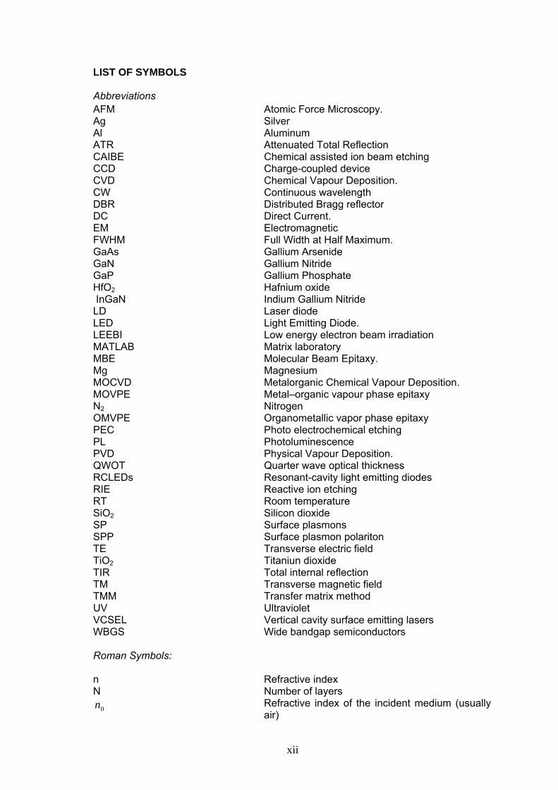
LIST OF SYMBOLS Abbreviations AFM Atomic Force Microscopy. Ag Silver Al Aluminum ATR Attenuated Total Reflection CAIBE Chemical assisted ion beam etching CCD Charge-coupled device CVD Chemical Vapour Deposition. CW Continuous wavelength DBR Distributed Bragg reflector DC Direct Current. EM Electromagnetic FWHM Full Width at Half Maximum. GaAs Gallium Arsenide GaN Gallium Nitride GaP Gallium Phosphate HfO2 Hafnium oxide InGaN Indium Gallium Nitride LD Laser diode LED Light Emitting Diode. LEEBI Low energy electron beam irradiation MATLAB Matrix laboratory MBE Molecular Beam Epitaxy. Mg Magnesium MOCVD Metalorganic Chemical Vapour Deposition. MOVPE Metal–organic vapour phase epitaxy N2 Nitrogen OMVPE Organometallic vapor phase epitaxy PEC Photo electrochemical etching PL Photoluminescence PVD Physical Vapour Deposition. QWOT Quarter wave optical thickness RCLEDs Resonant-cavity light emitting diodes RIE Reactive ion etching RT Room temperature SiO2 Silicon dioxide SP Surface plasmons SPP Surface plasmon polariton TE Transverse electric field TiO2 Titaniun dioxide TIR Total internal reflection TM Transverse magnetic field TMM Transfer matrix method UV Ultraviolet VCSEL Vertical cavity surface emitting lasers WBGS Wide bandgap semiconductors Roman Symbols: n Refractive index N Number of layers
0n Refractive index of the incident medium (usually air)
xiii
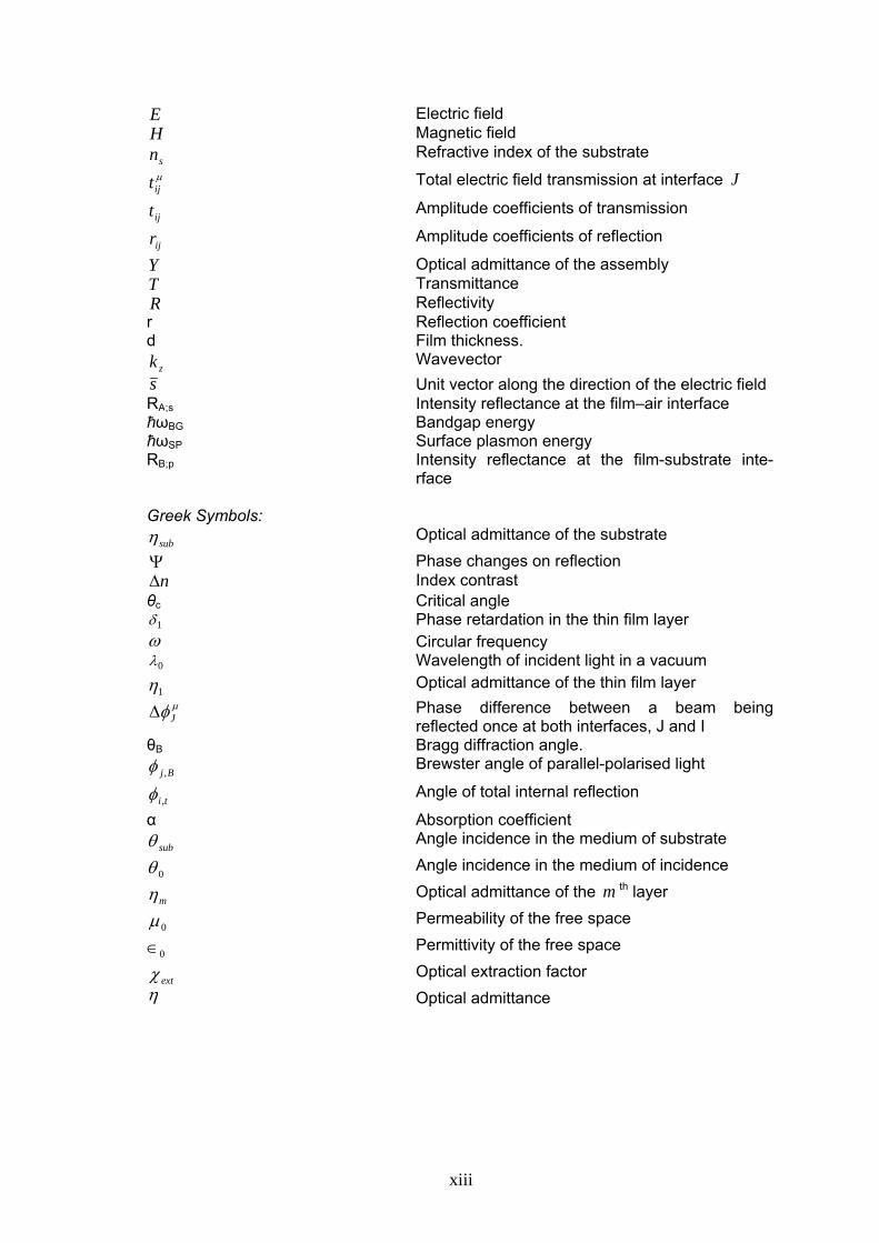
E Electric field H Magnetic field
sn Refractive index of the substrate μijt Total electric field transmission at interface J
ijt Amplitude coefficients of transmission
ijr Amplitude coefficients of reflection
Y Optical admittance of the assembly T Transmittance R Reflectivity r Reflection coefficient d Film thickness.
zk Wavevector s Unit vector along the direction of the electric field RA;s Intensity reflectance at the film–air interface ħωBG Bandgap energy ħωSP Surface plasmon energy RB;p Intensity reflectance at the film-substrate inte-
rface Greek Symbols:
subη Optical admittance of the substrate
Ψ Phase changes on reflection nΔ Index contrast
θc Critical angle 1δ Phase retardation in the thin film layer ω Circular frequency
0λ Wavelength of incident light in a vacuum
1η Optical admittance of the thin film layer μφJΔ Phase difference between a beam being
reflected once at both interfaces, J and I θB Bragg diffraction angle.
Bj ,φ Brewster angle of parallel-polarised light
ti,φ Angle of total internal reflection
α Absorption coefficient subθ Angle incidence in the medium of substrate
0θ Angle incidence in the medium of incidence
mη Optical admittance of the m th layer
0μ Permeability of the free space
0∈ Permittivity of the free space
extχ Optical extraction factor η Optical admittance
xiv
KAJIAN TENTANG REKABENTUK DAN EKSPERIMEN KE ATAS SALUTAN MULTI LAPISAN UNTUK APPLIKASI DEDALAM
PERANTI PEMANCAR CAHAYA GALLIUM NITRIDA
ABSTRAK
Dalam projek ini, cermin dan mikrorogga untuk peningkatan cahaya ultra-unggu
(UV) telah dibuat dan dikaji. Kerja yang dilakukan membincang kaedah rekabentuk dua
jenis cermin; jenis pertama ialah cermin pemantul Bragg teragih DBR (Al0.4Ga0.6N/
GaN) dan jenis kedua cermin dielektrik DBR (TiO2/SiO2, ZrO2/SiO2 dan HfO2/SiO2).
Sofwer MATLAB dan analisis teori berdasarkan kaedah Pindah Matriks (TMM)
digunakan untuk mengaji pantulan yang disebabkan ralat dalaman di mana ini berlaku
semasa penumbuhan filem, nombor lapisan, jenis substrak dan sudut tuju. Kami
anggap bahawa 10% ralat dalaman wujud pada bahan-bahan dengan indeks yang
rendah dan tinggi. Keputusan simulasi kami menunjukkan ralat dalaman menyebabkan
anjakan jalur pemantul sebanyak 36nm bagi struktur DBR semikonduktor dan 20nm
bagi struktur DBR dielektrik. Sifat-sifat optik Al0.11Ga0.89N, Al0.03Ga0.97N, dan GaN
tumbuh pada batu nilam dikajikan. Ukuran elipsometri beroperasi pada jarak
gelombang 632.8nm memperolehi ψ penukaran amplitud relative bagi pengutuban p
dan s, Δ anjakan fasa relatif di antara dua arah pengutuban dan indeks pemantulan,
parameter-parameter yang penting untuk memajukan model bagi GaN dan substrak
Al2O3. Kami telah menunjukkan peningkatan kecekapan ektrasi cahaya sebanyak 1.3 –
1.6 kali ganda dengan penggunaan epoksi rata dan kubah sebagai bahantara luar
banding dengan udara. Keputusan simulasi menunjukkan bahawa penggunaan HfO2
dan MgF2 dapat meningkatkan ekstrasi cahaya dengan membelau cahaya dalaman
dengan sudut pepejal yang besar ke dalam kon cahaya peleposan Tiga jenis
mikrorongga telah dibuat dengan penggunaan cermin logam dan DBR dielektrik untuk
peningkatan dan perencatan fotoluminescence pendarkilau (PL) dalam GaN. Struktur
GaN/nilam sebagai lapisan aktif dikapitkan di antara dua cermin pemantul logam

xv
perak. Lapisan GaN pada nilam menunjukkan puncak PL di sekitar 364 nm.
Pengukuran PL menunjukkan peningkatan 2 dan 16 kali ganda pada separuh rongga
cermin perak dan cermin DBR dielektrik, masing-masing. Di rongga penuh sampel, PL
amplitud di tingkatkan sebanyak 10 kali bila 50 nm perak digunakan sebagai cermin
hadapan. Peningkatan hebat yang melebihi 16 kali ganda diperolehi dengan
penggunaan cermin perak setebal 25 nm sebagai cermin hadapan. Selain daripada itu,
peningkatan hebat juga didapati dengan lubang kecil 4 mm2 dibuat di hadapan cermin
dengan tebal 50 nm.
xvi
DESIGN AND EXPERIMENTAL STUDIES OF MULTILAYER COATING FOR APPLICATIONS IN
GALLIUM NITRIDE LIGHT EMITTING DEVICES
ABSTRACT
In this work mirrors and microcavties for GaN-UV light enhancement were
fabricated and studied. This work discusses methods of designing two types of mirror:
first is the semiconductor distributed Bragg reflector (DBR) (Al0.4Ga0.6N/GaN) mirrors
and second is the dielectric DBR (TiO2/SiO2, ZrO2/SiO2, and HfO2/SiO2) mirrors.
MATLAB software and theoretical analysis based on Transfer Matrix Method (TMM)
are used to investigate reflection due to depth errors that occur in films growth, number
of layers, type of substrate and incidence angle. We assume that there is 10% depth
error in high and low index materials. Our simulation results showed that the depth
error caused the reflective band shift about 36nm for semiconductor DBR structure and
20nm for dielectric DBR structure. The optical properties of Al0.11Ga0.89N, Al0.03Ga0.97N,
and GaN grown on sapphire were investigated. The ellipsometry measurement
operating at wavelength 632.8nm yields ψ the relative amplitude change for p and s
polarizations, Δ relative phase shift between the two polarization direction and
refractive index, important parameters to develop the model for GaN on Al2O3
substrate. We demonstrated a GaN/sapphire microcavity exhibiting 1.3-1.6 fold
enhancement in light extraction efficiency by using flat and dome epoxy as external
medium compared with air as the external medium. Simulations results showed that by
using HfO2 and MgF2 can improve the light extraction by diffracting is the internal light
with a large solid angle into the escape light cone.
Three types of microcavity types were fabricated using metal and dielectric
DBR mirror for the enhancement and inhibition of photoluminescence in GaN. A
GaN/sapphire structure as an active layer was sandwiched between two mirrors, which
were silver metal reflectors. GaN layer on sapphire showed a photoluminescence (PL)
peak around 364 nm. Photoluminescence measurements showed intensity
xvii
enhancement of 2 and 16 fold in silver half-cavity back mirror and dielectric DBR mirror
respectively. In the full cavity samples, the amplitude of the photoluminescence is
enhanced 10-times when we used 50 nm silver as a front mirror. A tremendous
enhancement of more than 16-fold is obtained when silver mirror of 25nm thickness
was used as a front mirror. Further, a tremendous enhancement was obtained when a
small hole of 4mm2 was made in the front mirror with 50nm thickness.
1
CHAPTER ONE
INTRODUCTION 1.1 Introduction
Starting in early 20th century, there were several reports of light emission from
materials due to applied electric fields, a phenomenon that was termed
“electroluminescence”. The materials properties were poorly controlled, and the
emission processes were not well understood. The first light-emitting semiconductor
was a yellow-glowing piece of Silicon Carbide invented by Henry Joseph Round in
1907 (Herbert, 2002). There was not enough light to be useful, and silicon carbide is
hard to work with. In 1950’s the modern light emitting diodes LEDs were based on
Gallium Arsenide (GaAs) and emitted infrared light, red LEDs came next in 1960’s,
using Gallium Arsenide Phosphite (GaAsP on GaAs substrate). Eventually these led to
the development of high efficiency red, red-orange, and orange LEDs by changing to a
GaP substrate. Mid 1970's brought Gallium Phosphite (GaP) diodes, providing greater
efficiency. Mid 1980's saw the arrival of super high brightness (GaAlAsP) LEDs, first in
red, then yellow. In the early 1990's, ultra bright InGaAlP LEDs were made in orange-
red, orange, yellow and green. The first significant blue LEDs came in the early 1990's,
using Silicon Carbide. This was a throwback to the earliest semiconductor light
sources. The mid 1990's brought ultra bright blue GaN LEDs, then Indium Gallium
Nitride (InGaN) LEDs, producing high-intensity green and blue. Many activities have
been used on the fabrication of high brightness white/blue/green LEDs and laser
diodes (LDs) in blue and UV spectra for many applications. For these purposes, III-
nitride semiconductors such as gallium nitride (GaN) have been investigated for a long
time. For more than 50 years ago, GaN was first synthesized by Juza and Hahn, 1938
who passed ammonia over hot gallium. This method produced small needles and
platelets. Two decades later, Grimmeiss and Koelmans, 1959 studied the
photoluminescence spectra of GaN. In 1969, Maruska and Tietjen succeeded in
growing single crystalline GaN on sapphire using a chemical vapor deposition
2
technique. All the GaN films made at that time were very conductive n-type GaN
(undeliberately doped). The donors were believed to be nitrogen vacancies or oxygen
incorporation (Seifert et al., 1983). Soon after, Pankove et al., 1972, reported the first
GaN LEDs. The electroluminescence spectra of these LEDs could be varied from blue
to red depending on the Zn-doping concentration in the light-emitting region (Pankove,
1973). The modern progress of III nitrides began from Amano and Akasaki, (Amano et
al., 1986). They initiated organometallic vapor phase epitaxy (OMVPE) for the growth
of high quality GaN film on sapphire substrate by introducing a concept of AlN buffer
layer between sapphire and GaN film. The implementation of buffer layer not only
improves the crystal quality of the bulk film but also paves the way for p-type doping by
using magnesium (Mg) as an acceptor doping (Amano et al.1988). A few years later
Akasaki and Amano achieved Mg-doped p-type GaN with high conductivity using low
energy electron beam irradiation (LEEBI) (Amano et al.1989). Then, Amano and
Akasaki, 1990 demonstrated the first GaN p-n junction LED. The electroluminescence
of the device was dominated by a near band edge emission at 375 nm, which was
attributed to transitions involving injected electrons and Mg-associated centers in the p-
GaN region. Soon thereafter, Nakamura and his colleagues at Nichia Chemicals found
that thermal annealing GaN: Mg above 750°C in N2 or vacuum also converted the
material to conducting p-type (Nakamura,et al., 1992). It was this breakthrough that
made high brightness InGaN-based LEDs commercialize in 1994 (Nakamura, et al.,
1994). In 1996, the AlGaN/GaN/InGaN pulsed LD was first reported to operate at room
temperature (Itaya et al., 1996). An InGaN-based LD was soon successfully operated
under continuous wavelength (CW) mode (Nakamura, et al., 1996).
GaN and other III-nitrides are attractive in the fabrication of photonic and
microelectronic devices for the most of areas because the performances of these
devices are better than some of existing material systems such as Si and GaAs.
3
Physical, chemical and other interesting properties of GaN and related nitride materials
provide the basis for the design and development of optoelectronic devices. GaN and
related nitride materials can grow both in the crystalline wurtzite as well as zincblede
structures, but the wurtzite structure is more common. The lattice constant of GaN
wurtzite structure is shorter than that of GaN zincblede (Yoder, 1996). GaN and related
nitride materials are the wide bandgap semiconductors (WBGS) whose definition is that
the bandgap energy of material is larger than 3 eV. The III-nitride materials have high
bond energies compared to other semiconductors therefore; normal wet etching
methods is very difficult to pattern GaN and related nitrides for device fabrication
(Mileham, et al., 1996). Until now, photo electrochemical (PEC) etching (Minsky, et al.,
1999; Youtsey, et al., 1997) and 10% KOH in ethylene glycol in 165 °C (Stocker, et al.,
1998) are the only alternative and successful wet etching techniques to process GaN.
Because the sidewalls of PEC etching are very rough and high temperature of 10%
KOH solution is not realistic to achieve, thus, most devices are fabricated by the
techniques of plasma etching such as reactive ion etching (RIE), inductively coupled
plasma (ICP) etching, and chemical assisted ion beam etching (CAIBE). Because of
the GaN have direct band gap the luminous intensities of GaN-based LEDs are at least
10-100 times stronger than that of SiC LEDs and the external quantum efficiencies are
almost two orders of magnitude greater than the efficiency of SiC. Until recently, the
rapid increase in LED’s efficiency was mainly due to material improvements. The
saturated drift velocity is a parameter that shows the capability of device operation for
high frequency at high electrical field. The electron saturated drift velocity of GaN is
slightly better than that of GaAs, 8%-35% more than that of SiC, and 2.7 times higher
than that of Si. The breakdown electrical field of GaN is 10 times higher than that of
GaAs, 20 times larger than the breakdown field of Si. GaN presents lower dielectric
constant compared to Si and GaAs. The thermal conductivity of GaN is almost 3 times
higher than that of GaAs, roughly equal to that of Si, but less than one-third that of SiC.
The coefficient of thermal expansion of GaN is smaller than that of GaAs and Si,
4
however, it exceeds 33% more than that of SiC. In wide bandgap semiconductors, GaN
and SiC are always competitors on the applications of power devices. The direct
bandgap and emission spectra of the photo electronic devices in the UV and visible
ranges are the advantages on the applications of color displays and photodetectors
(Walker, et al., 1996; Monroy, et al., 1999). In addition, nitride semiconductor-based
LEDs have proven to be reliable in such applications as displays, lighting, indicator
lights, advertisement, and traffic signs/signals There are currently major development
programs in the world for three newer applications for GaN-based materials and
devices (Pearton, et al., 2002), namely UV optical sources capable of operation down
to 280 nm for use in airborne chemical and biological sensing systems, allowing direct
multi-wavelength spectroscopic identification and monitoring of UV-induced reactions.
After giving a brief history of LED in general and GaN LED in particular, based on the
properties of GaN that have been mentioned earlier in brief, GaN is deemed a key
substance which has many applications, for example as a source of light operates
within a wide range of spectrum depending on the mole fraction added such as (Al) and
(In) to alter its energy gap. Now, modern growth techniques can achieve very high
quality material deposition, giving active zones with almost 100% internal quantum
efficiency, meaning that each electron-hole pair entering the active zone recombines
radiatively by producing a photon. Then, the main limitation in efficiency comes from
the optical extraction factor that gives the probability for an internal photon to be
extracted in the outside medium. Because GaN has high refractive index it is not easy
to extract light from it effectively and due to certain factors that determine light quantity
emitted out of this substance. The main factors are the design and structure of this
substance. The efficiency of “conventional” LEDs is limited to (1/4n2)~4% where n is
the refractive index of the active medium (Maxime et al., 2002). The remainder of
internally generated light (92%–96%) never finds an opportunity to escape the emitter,
and is eventually absorbed, either by the active region or the opaque substrate. For
years, a significant amount of scientific work has been focused on ways of improving
5
the extraction efficiency of light-emitting diode (LED). ). Many interesting approaches
have been proposed to accomplish this, such as the use of thin light emitting layers
with surface texturing (Schnitzer et al., 1993), resonant cavities (Temelkurana and
Ozbay, 1998) and photon recycling (Misha et al., 1999).
This efficacy mainly depends on light reflection inside the active medium and
emitting it out. Therefore the researcher tends to look for increasing the reflectivity
inside the gap by using the multi-layer mirror DBR that encompasses the active
medium on both ends to exploit this medium optimally. To design these DBR layers
and to select its materials, there must be certain theoretical calculations through which
we will be able to know the number of these layers and the ultimate reflectivity these
layers provide.
The possibility of ratio error while manufacturing large number of DBR layers
demand high cost of this kind of mirror which is needful to achieve high reflectivity.
Through the technological development, knowing more about the materials and their
properties, we can use different types of materials to achieve high reflectivity. So using
the metallic reflectors in increasing the reflectivity and enhance the light emission is a
cheaper and practical option. Aluminum, gold and silver are the most used metals for
reflective coatings (Macleod, 1986).
The objectives of the thesis are as follows:
1- Simulation of DBR for semiconductors (GaN /AlxGa1-xN) and dielectric
(TiO2/SiO2, ZrO2/SiO2, HfO2/SiO2) materials to achieve high reflectivity.
2- Simulation of GaN microcavity using external materials (HfO2, MgF2, and
epoxy).
6
3- Characterization of GaN material as active mediums using different optical
techniques (ellipsometry, filmetrics, spectrophotometer, and photolumines-
cence).
4- Fabrication and measurement of metal/sapphire and dielectric/sapphire DBR
mirrors.
5- Design and fabrication of half and full microcavities on GaN using metal and
dielectric DBR mirrors to get high extraction efficiency.
6- Fabrication of external medium using epoxy in order to get high extraction
efficiency from the active medium.
The originality of our work is firstly, using the silver as a contact and as a
resonator instead of multilayer semiconductor or dielectric materials to enhance the
extraction efficiency from GaN active layer. Secondly, in our microcavity design we
have used the sapphire substrate as a spacer between the back mirror and the active
medium to get resonance condition to achieve standing wave inside the active medium
and enhance the extracted light.
This thesis is organized as follows: In chapter 2, TMM theory of the DBR optical
multilayer and calculation on reflectivity and transmissivity will be presented. Chapter 3
describes the results from MATLAB programs to simulate and analize the effects of
variation of certain parameters on DBR efficiency. This will provide sufficient
background to enable one to understand the microcavity operation and the effects of
these parameters on UV light emission enhancement. Chapter 4 discusses the
fabrication and measurement results of the active medium and the dielectric DBR and
metal (Ag, Al) mirrors. Chapter 5 focuses on results of PL intensity enhancement using
metal (Ag, Al) and dielectric DBR mirrors in microcavity to enhance the spontaneous
UV emission in GaN samples. Finally, Chapter 6 concludes the thesis, with summary
and future work.
7
CHAPTER TWO
MULTILAYER STRUCTURE AND MICROCAVITY DESIGN 2.1 Introduction This chapter discusses the optical properties of thin films and how their unique
characteristics can be used to develop the reflectivity, and enhance the extracted light
using microcavity. One of the most important and pervasive sub-fields of optical
science is the technology of thin film. It is very rare to find any optical system in today’s
technology that does not have components with single or multilayer thin films attached.
The physical phenomena that describe the basis of filters (mirrors) include
absorption, refraction, diffraction, scattering and polarization. The optical performances
of thin film filters are determined by the interference that occurs because of multiple
reflected beams at the various interfaces within the film coating (Flory, 1995; Conway,
1999). However the most complete descriptions of the performance of these filters are
provided by the spectral reflectance, transmittance, absorption and phase shift on
reflection (Macleod, 2000; Furman et al., 1992). This section briefly details the basic
theory, which is necessary in order to make calculations of the properties of multilayer
thin film filters.
2.2 Optical parameters of thin films
The theoretical and experimental studies on the optical behaviors of thin films deal
primarily with optical reflection, transmission, and absorption properties, and their
relation to the thickness and optical constants of films. Consequently, complex
multilayer optical-device systems with remarkable reflection, antireflection, interference,
and polarization properties have emerged for both laboratory and industrial
applications. The simplest and commonest type of optical coating is probably the thin
metal layer that is used as a reflector. Metals attenuate very rapidly any light that
succeeds in passing through their front surface. Thus a thin metal film will usually have
optical properties indistinguishable from those of the bulk material. Almost other thin
8
film optical coatings depend on interference for their operation. In an optical coating,
the particular materials used for the thin film vary with the application and
consideration, such as the environment in which the coating will be used, frequently
imply that the choice of materials should be as much for their mechanical as for their
optical properties. It is possible to construct assemblies of thin films which will reduce
the reflectance of surface and hence increase the transmittance of a component, or
increase the reflectance of a surface, or which will give high reflectance and low
transmittance over part of a region and low reflectance and high transmittance over the
remainder, or which will have different properties for different planes of polarization and
so on (Thelen, 1988). Thin film coating are often known by names which describe their
function, such as antireflection coatings, beam splitters, polarizer, long wave pass
filters, band-stop or minus filters, or which describe their construction, such as quarter-
wave attack or quarter-half quarter coating (Furman and Tikhonravov, 1992).
2.2.1 Refractive index
The indices of refraction are only properties of an optical material, which used in
actual design of optical system. A refracting material, to be useful, obviously must
transmit radiation in the wavelength region in which it is to be used. In some instances,
the refracting material transmits imperfectly in the region of use and the designer must
determine what thickness he can use without greatly impairing the performance of the
instrument. In most cases, the thickness and refractive index of the films in a multilayer
mirror are chosen from theoretical considerations. In order to translate this design into
a practical mirror, it is necessary to select for each layer a thin film material, which can
be evaporated to a desired thickness and which has a refractive index, which is close
to the theoretical value.
9
2.2.2 Quarter wave optical thickness and optical admittance
The principle of the single and multilayer reflection coatings is based on the
constructive interference of light reflected from the interfaces of the coating layers. Any
time light traverses an interface between two media with different refractive indexes,
such as the air/sapphire interface, a portion of the incident light is reflected. When this
incident light is normal to the surface, the amplitude of the reflected wave at the
interface between the sapphire substrate and the incident media is proportional to the
Fresnel amplitude reflection coefficient (r) (Born and Wolf, 1983):
)()(
0
0
s
s
nnnn
r+−
= (2-1)
where 0n is the refractive index of the incident medium (usually air), and sn is the
refractive index of the substrate, in this case sapphire. The human eye and most other
photodetectors, however, do not respond directly to the amplitude of light, but rather to
the intensity of light. The intensity of the reflected light, referred to as reflectivity )(R , is
equal to the square of the amplitude of the reflected light. The reflectivity of a bare
substrate, irradiated at normal incidence is given by,
20
202
)()(
1s
s
nnnn
TrR+−
=−== (2-2)
where T is the transmittance. For example, the amplitude of the light reflected off
uncoated sapphire ( 78.1=sn ) in air ( 10 =n ) is 28.0=r . The reflectivity in this
situation is 078.02 == rR , or 7.8%. Therefore, as far as the human eye and other
photodetectors are concerned, 7.8% of the light is reflected off the sapphire substrate.
When this sapphire substrate is coated with a thin layer (non-absorbing) film of different
index than the sapphire, the reflectivity is changed. The reflectivity of a surface coated
with a single layer having refractive index 1n and physical thickness 1t is given
(Macleod., 1986):
10
12
2
1011
220
12
2
1011
220
sincos)(
sincos)(1
δδ
δδ
⎟⎟⎠
⎞⎜⎜⎝
⎛+++
⎟⎟⎠
⎞⎜⎜⎝
⎛−+−
=−=
nn
nnnn
nn
nnnnTR
ss
ss
(2-3)
0
111 2
λπδ
tn= (2-4)
where 1δ is the phase retardation in the thin film layer,� and 0λ is the wavelength of
incident light in a vacuum. The product 11tn is referred to as the optical thickness of the
film.
This product is what determines the phase shift of a light beam as it traverses
the film. When the optical thickness of the layer is equal to ( 20λm ), where m is an
odd integer, the phase shift suffered by a wave traveling through thickness 1t of a thin
film is given by ( 011 /λπ tn− ), the phase shift multiple of 180º and the layer acts as an
absentee layer. In this case equation (2-3) reduces to equation (2-2) and the reflectivity
of the coated substrate is the same as that of the uncoated substrate. The optical
thickness 11tn is related to physical thickness by the refractive index. If the optical
thickness is ( 40λ ) then, 101 4/ nt λ= and the layer is referred to as having quarter
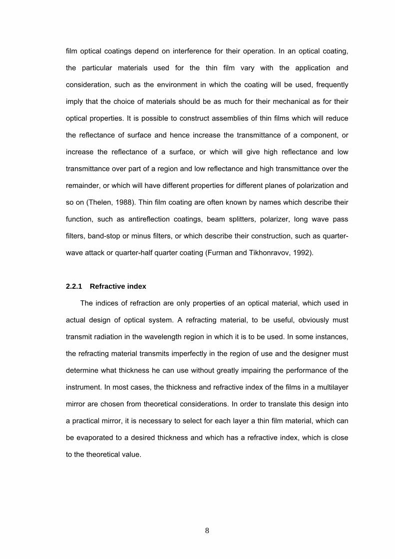
wave optical thickness (QWOT). Fig. 2.1 shows a comparison between the optical and
physical thickness of a film. The optical thickness is shown to be greater than its
physical thickness. This difference is compensated for by the fact that the wavelength
shown is not the wavelength in the film, but the wavelength in a vacuum.
11
Fig. 2.1: Comparison between physical and optical thickness in an optical film.
The optical thickness of the film is represented in (A) and the physical thickness
is shown in (B). The solid lines represent the wavelength of light in a vacuum, and the
dotted line represents the wavelength in the film. The wavelength of the incident light
after it has entered the film is represented by the dotted line. This illustrates that the
wavelength of the light decreases as it enters the film.
The wavelength ( iλ ) of the incident light as it propagates through the thin film
layer is 10 / ni λλ = . It is usual to define some extra quantities to reduce the notation of
the reflectance and transmittance expressions. Instead of the refractive index, it is
common to use the quantity )/( μη cn= (ratio of magnetic field to electric field
strengths) known as the characteristic optical admittance of the medium. In free space,
the optical admittance is (Liddell, 1980):
21)(
0
00 μ
η∈
= =2.6544x10⁻³ S (2-5)
0∈ and 0μ are the permittivity and the permeability of the free space respectively.
12
And since )/(1 200 cμ=∈ and at optical frequencies 0μμ = , we can write:
0ηη n= (2-6)
The straightforward nature of the calculations when the layer is a quarter-wave
thick yields a particularly simple result that can be best expressed in terms of the
transformation of the admittance of the substrate. Optical quarter wave layer of
characteristic admittance η transform the admittance of the substrate surface from sη
to sηη /2 . This result is known as the quarter-wave rule and the reflectance of the
substrate coated with a single quarter-wave layer is then:
( )22
0
20
//
s
sRηηηηηη
+−
= (2-7)
We can extend the idea of admittance transformation by optical quarter wave
layer to a stack of quarter waves.
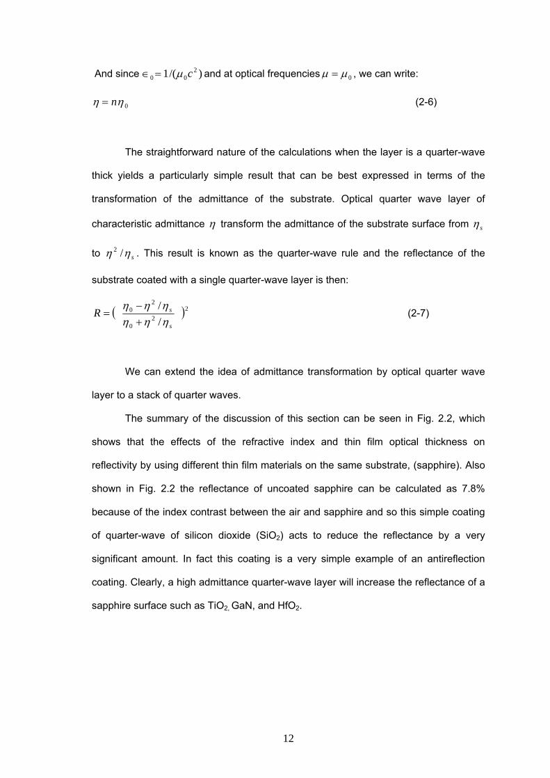
The summary of the discussion of this section can be seen in Fig. 2.2, which
shows that the effects of the refractive index and thin film optical thickness on
reflectivity by using different thin film materials on the same substrate, (sapphire). Also
shown in Fig. 2.2 the reflectance of uncoated sapphire can be calculated as 7.8%
because of the index contrast between the air and sapphire and so this simple coating
of quarter-wave of silicon dioxide (SiO2) acts to reduce the reflectance by a very
significant amount. In fact this coating is a very simple example of an antireflection
coating. Clearly, a high admittance quarter-wave layer will increase the reflectance of a
sapphire surface such as TiO2, GaN, and HfO2.
13
Fig. 2.2: The reflectance of single films of different index on sapphire as a function of optical thickness.
2.3 Transfer matrix method (TMM)
2.3.1 Single and double layers reflectivity
Optical filters can be defined as thickness dependent refractive index systems,
which modify the properties of a surface to produce the desired optical characteristics.
As discussed previously, thin film interference filters are highly popular for applications
in a range of fields. These filters can work over a broad range of wavelengths or over a
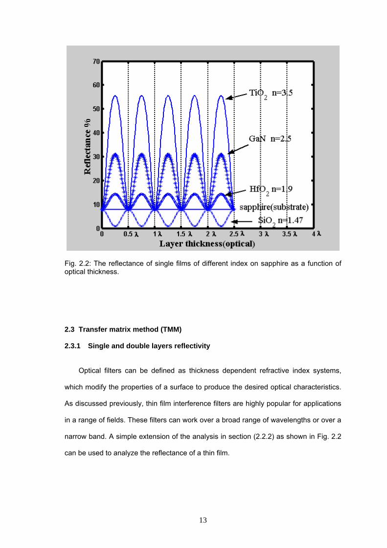
narrow band. A simple extension of the analysis in section (2.2.2) as shown in Fig. 2.2
can be used to analyze the reflectance of a thin film.
14
E a+
1 E b+
1
E b−
1
E a−
1 H b+
1
H b−
1H a−
1
H a+
1
Boundarya
Boundaryb
SubstrateFilmAir
n0 n1 n s
Fig. 2.3: Plane wave incident on a thin film
The successive reflections at the multiple interfaces give rise to multiple beams
and the summation of these beams determines the properties of the film. The film is
said to be ‘thin’ when interference effects can be observed in the beams. When
monochromatic, plane polarized light passes through a thin film, multiple reflections at
the interfaces give rise, generally, to two main beams of light advancing in opposite
directions. At any point within the medium, these beams will interfere and give rise to a
resultant electric field E and a resultant magnetic field H. Considering the light to be
incident normally to the surface; the field vectors are parallel to the interfaces.
The arrangement is illustrated in Fig. 2.3. At this stage it is convenient to
introduce a new notation. We denote waves in the direction of incidence by the symbol
+ (that is, positive-going) and waves in the opposite direction by – (that is, negative-
going). The interface between the films and the substrate, denoted by the symbol “b”,
15
can be treated in exactly the same way as the simple boundary in a and b. We
consider the tangential components of the fields. There is no negative-going wave in
the substrate and the waves in the film can be summed into one resultant positive-
going wave and one resultant negative-going wave. At this interface, then, the
tangential components of E and H are −+ += bbb EEE 11 (2-8)
−+ −= bbb HHH 1111 ηη (2-9)
where 1η is the optical admittance of the thin film layer which is defined by the optical
admittance of the free space ( 377/10 =η siemens) as:
011 ηη n= (2-10)
At normal incident angle, the optical admittance is usually normalized to equal
the same numerical magnitude as the refractive index. At oblique incidence angles, the
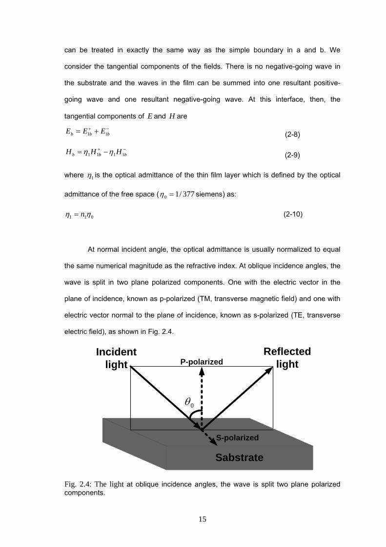
wave is split in two plane polarized components. One with the electric vector in the
plane of incidence, known as p-polarized (TM, transverse magnetic field) and one with
electric vector normal to the plane of incidence, known as s-polarized (TE, transverse
electric field), as shown in Fig. 2.4.
Sabstrate
Incidentlight
ReflectedlightP-polarized
S-polarized
0θ
Fig. 2.4: The light at oblique incidence angles, the wave is split two plane polarized components.
16
The optical admittance at oblique incidence angle can be expressed as:
1011 cosθηη n= for s-polarization (2-11)
1011 cos/)( θηη n= for p-polarization (2-12)
where 1θ is the angle of incidence in the thin film layer, which is related to the angles of
incidence in the medium of incidence 0θ and in the substrate subθ by Snell’s laws
(Heavens, 1955):
1100 sinsin θθ nn = (2-13)
subsubnn θθ sinsin 11 = (2-14)
From equations (2-8) and (2-9), where we are neglecting the common phase
factors we can obtain the expression for the traveling waves (Ulaby, 1999):
⎟⎟⎠
⎞⎜⎜⎝
⎛+=+
bb
b EH
E1
1 21
η (2-15)
⎟⎟⎠
⎞⎜⎜⎝
⎛+−=−
bb
b EH
E1
1 21
η (2-16)
Hence:
( )bbbb EHEH 1111 21 ηη +== ++ (2-17)
( )bbbb EHEH 1111 21 ηη −=−= −− (2-18)
these are the amplitude terms for the fields at the interface “b”. A wave traveling inside
the material exponential fall-off amplitude, therefore the expression of the fields at
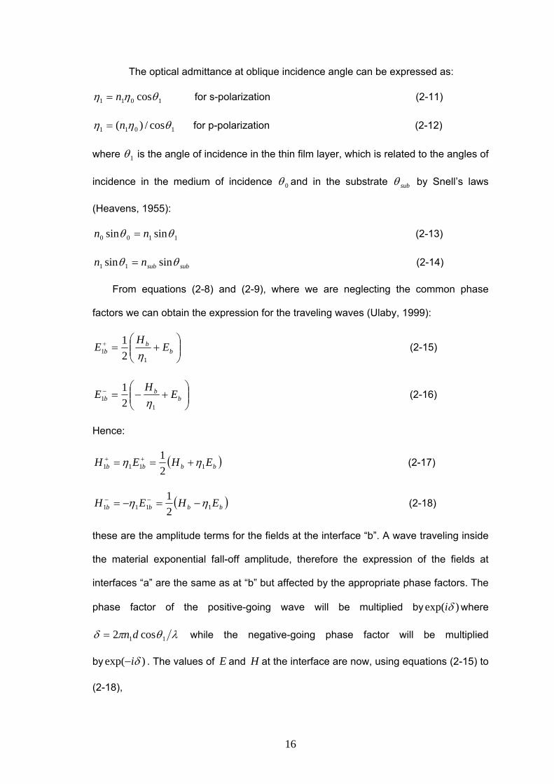
interfaces “a” are the same as at “b” but affected by the appropriate phase factors. The
phase factor of the positive-going wave will be multiplied by )exp( δi where
λθπδ 11 cos2 dn= while the negative-going phase factor will be multiplied
by )exp( δi− . The values of E and H at the interface are now, using equations (2-15) to
(2-18),
17
δδ
ηi
bbi
ba eEH
eEE ⎟⎟⎠
⎞⎜⎜⎝
⎛+== ++
111 2
1 (2-19)
δδ
ηi
bbi
ba eEH
eEE −−−−⎟⎟⎠
⎞⎜⎜⎝
⎛+−==
111 2
1 (2-20)
( ) δδ ηη ibbb
iba eEHEeHH 11111 2
1+=== +++ (2-21)
( ) δδ ηη ibbb
iba eEHEeHH −−−−− −=−== 11111 2
1 (2-22)
The resultant field in “a” are:
⎟⎟⎠
⎞⎜⎜⎝
⎛ −+⎟⎟
⎠
⎞⎜⎜⎝
⎛ +=+=
−−−+
111 22 η
δδδδ ii
b
ii
baaaeeHeeEEEE
1
sincosηδδ iHE bb += (2-23)
⎟⎟⎠
⎞⎜⎜⎝
⎛ ++⎟⎟
⎠
⎞⎜⎜⎝
⎛ −=+=
−−−+
1111 22 η
ηδδδδ ii
b
ii
baaaeeHeeEHHH
δδη cossin1 bb HiE += (2-24)
This can be written in matrix notation, defining the whole thin film between the
‘boundary a’ and ‘boundary b’ as shown in Fig. 2.3 which is given by:
⎥⎥⎥
⎦
⎤
⎢⎢⎢
⎣
⎡
δδηηδδ
cossin
sincos
1
1
i
i (2-25)
Therefore, we can write the matrix for single layer as,
⎥⎦
⎤⎢⎣
⎡
⎥⎥⎥
⎦
⎤
⎢⎢⎢
⎣
⎡=⎥
⎦
⎤⎢⎣
⎡
b
b
a
a
HE
i
i
HE
δδηηδδ
cossin
sincos
1
1 (2-26)
18
Since the tangential components of E and H are continuous across a
boundary, and since there is only a positive-going wave in the substrate, this
relationship connects the tangential components of E and H at the incident interface
with the tangential components of E and H , which are transmitted through the final
interface. The 2x2 matrix on the right-hand side of equation (2-26) is known as the
characteristic matrix of the thin film.
We define the input optical admittance Y of the assembly as
a
a
EH
Y = (2-27)
when the problem becomes merely that of finding the reflectance R of a simple
interface between an incident medium of admittance 0η and a medium of admittance
Y , i.e.
YY
r+−
=0
0
ηη
(2-28)
*
0
0
0
0⎟⎟⎠
⎞⎜⎜⎝
⎛+−
⎟⎟⎠
⎞⎜⎜⎝
⎛+−
=YY
YY
Rηη
ηη
(2-29)
We can normalize equation (2-26) by dividing by bE to give
bsub
a Ei
iCB
YE ⎥
⎦
⎤⎢⎣
⎡⎥⎦
⎤⎢⎣
⎡=⎥⎦
⎤⎢⎣⎡=⎥
⎦
⎤⎢⎣
⎡=
ηδδηηδδ 1
cossin/)sin(cos1
1
1 (2-30)
B and C , the normalized electric and magnetic fields at the front interface, are the
quantities from which we will be extracting the properties of the thin-film system.
Clearly, from (2-27) and (2-30), we can write
δηηδδηδη
sin)/(cossincos
1
1
sub
ubs
ii
Y+
+= (2-31)
and from (2-29) and (2-31) we can calculate the reflectance.
19
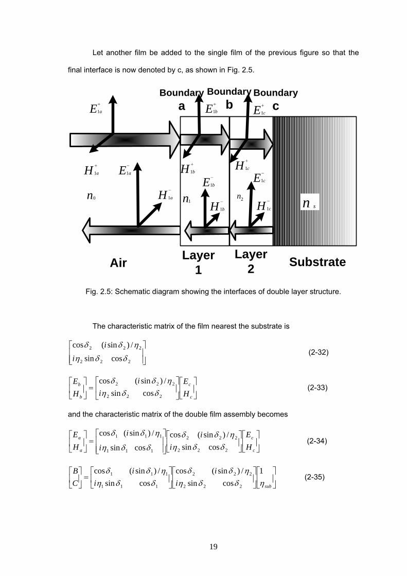
Let another film be added to the single film of the previous figure so that the
final interface is now denoted by c, as shown in Fig. 2.5.
E a+
1 E b+
1
E b
−
1
E a
−
1 H b
+
1
H b
−
1
H a
−
1
H a
+
1
Boundarya
Boundaryb
SubstrateLayer1Air
n0 n1 n s
Boundaryc
Layer2
2n
H c
+
1
E c+
1
H c
−
1
E c
−
1
Fig. 2.5: Schematic diagram showing the interfaces of double layer structure.
The characteristic matrix of the film nearest the substrate is
⎥⎥⎦
⎤
⎢⎢⎣
⎡
222
222
cossin
/)sin(cos
δδη
ηδδ
i
i (2-32)
⎥⎦
⎤⎢⎣
⎡⎥⎦
⎤⎢⎣
⎡=⎥
⎦
⎤⎢⎣
⎡
c
c
b
b
HE
ii
HE
222
222
cossin/)sin(cos
δδηηδδ
(2-33)
and the characteristic matrix of the double film assembly becomes
⎥⎦
⎤⎢⎣
⎡⎥⎦
⎤⎢⎣
⎡
⎥⎥⎦
⎤
⎢⎢⎣
⎡=⎥
⎦
⎤⎢⎣
⎡
c
c
a
a
HE
ii
i
i
HE
222
222
111
111
cossin/)sin(cos
cossin
/)sin(cos
δδηηδδ
δδη
ηδδ (2-34)
⎥⎦
⎤⎢⎣
⎡⎥⎦
⎤⎢⎣
⎡⎥⎦
⎤⎢⎣
⎡=⎥
⎦
⎤⎢⎣
⎡
subii
ii
CB
ηδδηηδδ
δδηηδδ 1
cossin/)sin(cos
cossin/)sin(cos
222
222
111
111 (2-35)
20
Y , is as before equal to BC / , and the amplitude reflection coefficient and the
reflectance are the same equations above. The result can be immediately extended to
the general case of an assembly of N layers.
2.3.2 Multilayer calculation
2.3.2.1 Distributed Bragg Reflector (DBR) mirror
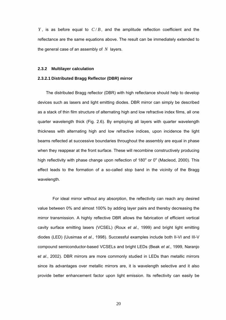
The distributed Bragg reflector (DBR) with high reflectance should help to develop
devices such as lasers and light emitting diodes. DBR mirror can simply be described
as a stack of thin film structure of alternating high and low refractive index films, all one
quarter wavelength thick (Fig. 2.6). By employing all layers with quarter wavelength
thickness with alternating high and low refractive indices, upon incidence the light
beams reflected at successive boundaries throughout the assembly are equal in phase
when they reappear at the front surface. These will recombine constructively producing
high reflectivity with phase change upon reflection of 180o or 0o (Macleod, 2000). This
effect leads to the formation of a so-called stop band in the vicinity of the Bragg
wavelength.
For ideal mirror without any absorption, the reflectivity can reach any desired
value between 0% and almost 100% by adding layer pairs and thereby decreasing the
mirror transmission. A highly reflective DBR allows the fabrication of efficient vertical
cavity surface emitting lasers (VCSEL) (Roux et al., 1999) and bright light emitting
diodes (LED) (Uusimaa et al., 1998). Successful examples include both II-VI and III-V
compound semiconductor-based VCSELs and bright LEDs (Beak et al., 1999, Naranjo
et al., 2002). DBR mirrors are more commonly studied in LEDs than metallic mirrors
since its advantages over metallic mirrors are, it is wavelength selective and it also
provide better enhancement factor upon light emission. Its reflectivity can easily be
21
controlled and increasing reflectivity doesn’t result in absorption losses compared to
metallic mirrors.
This section will look into the DBR design and investigate its reflectivity and
transmission properties. The parameters that determined and performance high
reflectivity are thickness, number of layers and optical parameters.
High index
Low index
Substrate
Incidence light
Reflected light
Fig. 2.6: DBR mirror structure
Various methods have been developed to calculate the multilayer reflectivity
and the most convenient method is the matrix method. The matrix method for
calculating the spectral coefficients of the layered media was first suggested by
(Berreman, 1986) and has been widely employed ever since.
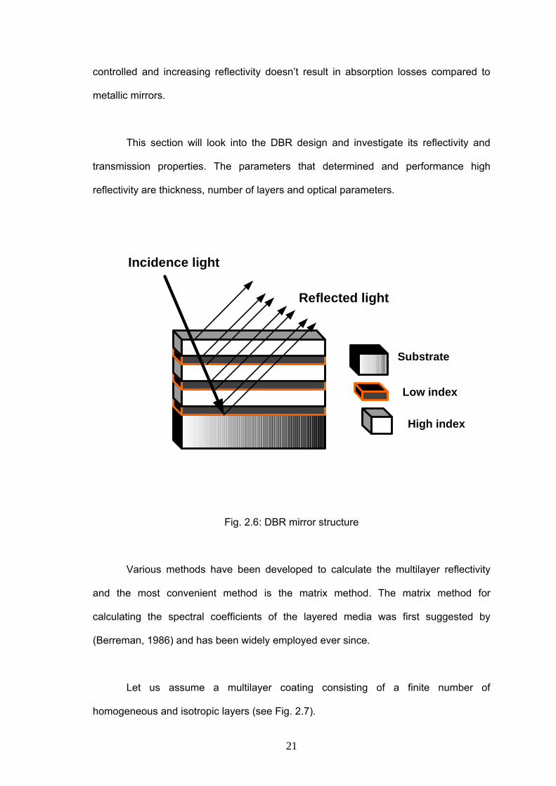
Let us assume a multilayer coating consisting of a finite number of
homogeneous and isotropic layers (see Fig. 2.7).
22
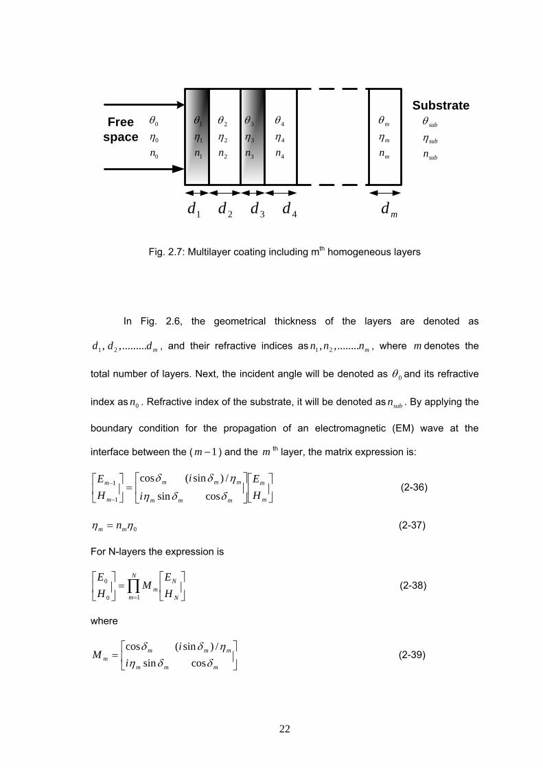
0
0
0
nηθ
1
1
1
nηθ
2
2
2
nηθ
3
3
3
nηθ
4
4
4
nηθ
m
m
m
nηθ
mddddd 4321
Freespace
Substrate
sub
sub
sub
nηθ
Fig. 2.7: Multilayer coating including mth homogeneous layers
In Fig. 2.6, the geometrical thickness of the layers are denoted as
mddd .........,, 21 , and their refractive indices as mnnn ........,, 21 , where m denotes the
total number of layers. Next, the incident angle will be denoted as 0θ and its refractive
index as 0n . Refractive index of the substrate, it will be denoted as subn . By applying the
boundary condition for the propagation of an electromagnetic (EM) wave at the
interface between the ( 1−m ) and the m th layer, the matrix expression is:
⎥⎦
⎤⎢⎣
⎡⎥⎦
⎤⎢⎣
⎡=⎥
⎦
⎤⎢⎣
⎡
−
−
m
m
mmm
mmm
m
m
HE
i
iHE
δδη
ηδδ
cossin
/)sin(cos
1
1 (2-36)
0ηη mm n= (2-37)
For N-layers the expression is
⎥⎦
⎤⎢⎣
⎡=⎥
⎦
⎤⎢⎣
⎡∏= N
NN
mm H
EM
HE
10
0 (2-38)
where
⎥⎦
⎤⎢⎣
⎡=
mmm
mmmm i
iM
δδηηδδ
cossin/)sin(cos
(2-39)
23
and
ssN
N EHE
⎥⎦
⎤⎢⎣
⎡=⎥
⎦
⎤⎢⎣
⎡η1
(2-40)
where mδ is the phase shift of the EM wave at the interface obtained from equation (2-
4). From equation 2-37 we can obtained mη and sη which is the optical admittance of
the m th layer and the substrate respectively. Equation 2-40 can be expressed as:
ss
N EY
E ⎥⎦
⎤⎢⎣
⎡=⎥
⎦
⎤⎢⎣
⎡η11
(2-41)
Where Y is the characteristic optical admittance defined by equation 2-37. For a
general case of assembly of N layers, the characteristic matrix is simply the product of
the individual matrices taken in the correct order and is denoted by:
⎥⎦
⎤⎢⎣
⎡
⎭⎬⎫
⎩⎨⎧
⎥⎦
⎤⎢⎣
⎡=⎥
⎦
⎤⎢⎣
⎡ ∏= s
N
m mmm
mmm
ii
CB
ηδδηηδδ 1
cossin/)sin(cos
1
(2-42)
B and C are the total electric and magnetic field amplitudes; their ratio has the
dimension of admittance.
BCY /= (2-43)
Y is the admittance presented to the incident wave by the coating. The admittance
presented by simple interface between two media is indistinguishable from the
reflectance at that interface. This concept is used to calculate the reflectance of an
assembly of thin films and the transmittance and be derived through the relationship of
)1( RT −= . The expressions for reflectance, transmittance and phase changes on
reflection are given respectively as follows:
24
∗
⎥⎦
⎤⎢⎣
⎡+−
⎥⎦
⎤⎢⎣
⎡+−
=CBCB
CBCB
R0
0
0
0
ηη
ηη
(2-44)
∗++=
))((Re4
00
0
CBCBT sub
ηηηη
(2-45)
Where “∗ “denote the conjugate and the phase changes on reflection are then given
by:
⎥⎦
⎤⎢⎣
⎡+−
=ΨCBCB
0
0argηη
(2-46)
2.3.2.2 MATLAB simulation programs
Part of this thesis is to model and investigate the DBR mirror properties of
microcavity enhancement. It was decided that simulation via a software program would
be the best option. Previous section showed that the theory and formulas could be
used to accurately determine the reflectivity performance of an assembly of layers.
The design of thin-film multilayer coating often specifies the transmittance and
reflectance values at a number of wavelengths, angles, and polarizations of the
incident light. Hence, the MATLAB programs are written as a function of the
parameters that can be used to reach these goals, such as the number of layers in the
multilayer, the layer thicknesses, and the refractive indices of the individual layers and
surrounding media. The following sections outline the basic structure of MATLAB
programs a step by step approach will be adopted using equation shown in the
previous section. The MATLAB source codes for calculating reflectivity of the DBR
mirrors are enclosed in Appendix A. MATLAB source codes for phase shift of DBR
mirrors are enclosed in Appendix B. The progressive steps, taken to obtain the
program are outlined in the flowchart of Fig. 2.8.