Embed Size (px)
Citation preview

Design and Development of a High-Voltage Transformer-less Power Supply for ... 387
http://dx.doi.org/10.6113/JPE.2012.12.3.387
JPE 12-3-2
Design and Development of a High-Voltage Transformer-less Power Supply for Ozone
Generators Based on a Voltage-fed Full Bridge Resonant Inverter
Muhammad Amjad*,**, Zainal Salam†, Mochammad Facta*, and Kashif Ishaque*
†*Dept. of Energy Conversion, Faculty of Electrical Engineering, Universiti Teknologi Malaysia, Johor, Malaysia **University College of Engineering and Technology, The Islamia University of Bahawalpur, Bahawalpur, Pakistan
Abstract
It is known that transformer based power supplies for ozone generators have low efficiency, high cost and exhibits a limited frequency range of operation. To overcome these disadvantages, this paper proposes a high frequency ozone generator with the absence of a transformer. The voltage step-up is achieved only by utilizing the resonant tank. This is made possible by a novel
combination of ozone chamber materials that allow ozone to be generated at only 1.5 3.5 kVp-p. The input to the resonant tank is driven by a PWM full bridge resonant inverter. Furthermore, zero-current zero-voltage switching (ZCZVS) operation is achieved by employing a duty factor of 25% between the switches of the full bridge. The advantages of the proposed system include high efficiency, low cost and the ability to control ozone production by varying the input voltage to the inverter. The prototype is verified by both simulation and experimental results. Key words: Full bridge inverter, High voltage transformer, Ozone chamber, Ozone generation, Resonant tank, Zero-current
switching (ZCS), Zero-voltage switching (ZVS)
I. INTRODUCTION
Ozone gas (O3) is one of the strongest oxidizing and bleaching agents. It is used in many sectors such as agriculture, water supply, waste treatment and pharmaceuticals [1]-[3]. O3 is generated naturally in the environment by lightening or ultra violet (UV) radiation. Electrically, it can be produced by applying a high potential between two electrodes in an air or oxygen gas chamber, one of which is covered with a thin dielectric material. The space between electrodes, where the gas flows is called the discharge gap. This method of producing O3 is known in the
literature as corona discharge, atmospheric pressure glow discharge or dielectric barrier discharge (DBD). The latter, which is commonly referred to as silent discharge, has been proven to be the best method for ozone generation [4].
Currently, the main focus of most researcher is to obtain a high ozone yield using a minimum of energy. One possibility way to increase efficiency is to use a high frequency power supply to drive the ozone chamber. By increasing the frequency, the power density applied to the electrode surface is increased, allowing for a decrease in the applied electrode voltage. Due to the bombardment of electrons, the current flows through the discharge gap by means of millions of micro-discharge channels. High frequency operation tends to reignite the previously used micro-discharge channels and as a result the ozone yield is increased [5]. Manuscript received Mar. 14, 2011; revised Jan. 31, 2012
Recommended for publication by Associate Editor Yong-Chae Jung. †Corresponding Author: [email protected] Tel: +607-5536187, Fax: +607-5566272, Universiti Teknologi Malaysia *Dept. of Energy Conversion, Faculty of Electrical Engineering, Universiti Teknologi Malaysia, Malaysia. **University College of Engineering and Technology, The IslamiaUniversity of Bahawalpur, Pakistan
A typical ozone power supply consists of an inverter, coupled with a high turns-ratio transformer. In [6]-[8], a single switch class-E resonant inverter to supply the ozone chamber was presented. The main disadvantage of this topology is the high crest factor current that flows through the

388 Journal of Power Electronics, Vol. 12, No. 3, May 2012
switch, resulting in poor switch utilization. The switch turns on at a nonzero voltage and its output capacitance is not integrated in the resonance circuit. Furthermore, the voltage across the ozone chamber is not sinusoidal. The efficiency of the power stage is approximately 50%− thus limiting its application in the low power range. In [9], a similar topology was proposed but with an LC resonant tank placed at the secondary side of the transformer. The drawback of this circuit is the high voltage and current stresses in the switch. With the inclusion of an LC tank, its efficiency was increased but ZCZVS could not be achieved.
Fig. 1. Circuit diagram of the proposed ozone generator.
For multiple switch topologies, voltage-fed full bridge resonant inverters are the most popular [10]-[13]. In these circuits, the inductance is placed at the secondary of the transformer to stabilize the discharge. In [14]-[17], a full bridge inverter using a resonant inductor at the primary side is used to reduce the tuned resonant frequency. For both cases, the presence of the inductor increases the complexity of the circuit and reduces its efficiency. Ozone power supplies using current fed push-pull inverters are implemented in [4], [18]-[22]. However, the two inductors used as a choke are large, resulting in reduced efficiency.
All of the above-mentioned topologies used a high voltage transformer to achieve a high voltage for ozone generation. These transformers have high leakage inductances that cannot be integrated into the resonant tank because they have no path for flux discharge. Furthermore, high voltage spikes occur due to the leakage inductance, which greatly affect the commutation of the power switches. The transformer exhibits several other disadvantages, namely a limited frequency range of operation due to core saturation, a large size, a high parasitic capacitance and a low efficiency. Moreover, the capacitance of the ozone chamber is magnified by the step-up turn ratio of the transformer. As a result, it presents a high equivalent capacitance as seen from the input side. To alleviate these problems, an ozone power supply based on a piezoelectric transformer (PT) was proposed [23]. Although promising, the resonance bell of the PT is very narrow. As a result, the closed loop is difficult to control. PTs are very expensive and high power PT are not commonly available in the market.
Traditionally, borosilicate glass or ceramic is used as a dielectric material for the ozone chamber. For these materials, a peak voltage in the vicinity of 10 kV is required to initiate an electrical discharge for a 1 mm discharge gap. Recently, the use of mica as dielectric material has been proposed [24], [25]. Using this material, the initiation voltage (for natural air) for discharge is only around 1.5 kVp-p. The lower breakdown voltage of the mica provides an opportunity to experiment with new topologies for the power converters. Hence in this study, a transformer-less topology is considered.
The objective of this paper is to describe the design,
development, and analysis of a high-voltage transformer-less power supply for ozone generation. The required voltage gain is achieved using a resonance technique. No additional reactive element is required apart from the resonant tank. Other advantages of this topology include reduced cost, simpler design and increased reliability. Furthermore, the topology offers ZCZVS. The soft switching reduces losses and minimizes electromagnetic interference. Another benefit is the integration of the output capacitance of the power switches in the resonant circuit [20]. The soft switching is implemented using a class D-E inverter control. In theory, the efficiency could reach 100% [26], [ 27].
This paper is organized as follows: Section II outlines the overall proposed system and the ozone generator. Section III describes the analysis of the resonant tank and the ozone generator. The circuit operation is given in Section IV. Sections V and VI show the design and the implementation, respectively. Simulation and experimental results obtained from a prototype are given in section VII. Finally, the paper is summarized with conclusions in section VIII.
II. OVERALL PROPOSED OZONE GENERATION SYSTEM
The proposed ozone generator system is shown in Fig. 1. It consists of a high frequency PWM full bridge inverter, a resonant tank and an ozone chamber. The latter is modeled using a R-C in parallel.
A. PWM Full Bridge Inverter In the full bridge inverter, the MOSFETs M1, M3 and M2, M4
are switched in anti-phase to provide a quasi square wave as an input to the resonant tank. The switches are equipped with freewheeling diodes.
B. Resonant Tank
The resonant tank consists of a series Ls Cp circuit connected between the inverter and the ozone chamber. The high frequency square wave signal voltage multiplication is achieved by using the resonance. The resonant tank will also act as a filter. As a result, a sinusoidal voltage will appear across the chamber.

Design and Development of a High-Voltage Transformer-less Power Supply for ... 389
Fig. 4. Experimental setup to determine the ozone chamber parameters.
C. Ozone Chamber The ozone chamber basically consists of two electrodes
separated by a dielectric material. It behaves mainly like capacitive load [4]. The chamber used in this work is shown in Fig. 2. It consists of two aluminum mesh electrodes (outer side covered with copper tape) having a 120 mm length and a 70 mm width. One electrode is covered with muscovite mica having a 0.1 mm thickness. The discharge gap between electrodes is 1mm [24].
In [28], a high frequency model of the ozone chamber is
presented by a parallel combination of gC and gR . The
complete model for the proposed ozone chamber is shown in
Fig. 3. This simplified model is a linear one, in which gC
and gR are very easy to estimate. To obtain the values of gC
and gR , v ge charge (V-Q) and voltage-current (V-I)
Lissajous figures are used.
olta
The experimental setup to determine the chamber
parameters is shown in Fig. 4. The chamber capacitance gC
is calculated using:
max
( 0ch chg
i vC
V)
(1)
where the values of and can be obtained from
V-I Lissajous figure. The chamber resistance
chi maxV
gR is
determined by:
Fig. 2. Ozone chamber configuration.
Fig. 3. Ozone chamber configuration.
max
( 0ch
gc
VR
Q v
) (2)
where:
maxc mQ C V (3)
The values of and can be obtained from V-Q
Lissajous figure. For the chamber shown in Fig. 2, the
experimental results gives
mC maxV
gC = 0.242 nF and gR = 225 kΩ,
at a frequency of 30 kHz.
III. ANALYSIS OF THE RESONANT TANK AND OZONE CHAMBER CIRCUIT
A circuit diagram of the resonant tank and the equivalent circuit of the ozone chamber is shown in Fig. 5. The transfer function and the input impedance of this circuit is given by (4)
and (8), respectively [29]-[31].
22 2
p
( ) 1
( )
1
ov
in
p p
V jA
V j
Q
(4)
where ωp is the undamped natural frequency, given by:
1p
s tL C (5)
and Qp is the loaded quality factor, given by:

390 Journal of Power Electronics, Vol. 12, No. 3, May 2012
Fig. 5. Equivalent circuit of resonant tank and ozone
chamber.
gp
p s
RQ
L
p t gC R
g
(6)
where:
t pC C C (7)
2
2 2 2( )
11
g gin s
t
g tg t
R RZ j L
C
R CR C
(8)
Fig. 6. Voltage gain of circuit with respect to frequency for
Qp= 25, 8, 10.
The plot of (4) is shown in Fig. 6. It indicates that a large
voltage gain can be achieved near p
1pQ
and that the value
of is high at this point. For , andpQ p , (4)
becomes and (8) becomes, . This
shows that voltage gain is load dependent and is directly proportional to the load resistance near the resonance.
vA Q p2p inQ Z R g
The resonant frequency of the circuit can be found by taking the derivative of (4) with respect to and substituting
0vd d A and r :
2
11
2r ppQ
(9)
2
11
4
pvm
p
QA
Q
(10)
where r is the resonant frequency and is the
maximum voltage gain at this frequency. For pQ 0)
becomes:
vmA
1 , (1
vm pA Q (11)
IV. CIRCUIT OPERATION
The operating waveforms of the full bridge inverter are shown in Fig. 7. The equivalent circuits for each of the operating modes are shown in Fig. 8. An adequate duty factor is employed between the switches operation so that the reactive energy stored in the snubber capacitors and intrinsic capacitors of the switches can be handled without a loss of efficiency. In order to achieve ZCZVS operation, a switching frequency must be selected that is greater than ωr. The circuit operation can be divided into six modes as follows.
Mode 1 (t0 t1): During this mode M1 and M3 turn ON and the DC power supply provides energy to the load. This mode is called the rectifying mode. The current flows from the supply to the load via switches M1 and M3 and the voltage VAB is +VCC. The voltages across M1, M3, C1, C3, D1 and D3 are zero, and the voltages across M2, M4, C2, C4, D2 and D4 are +VCC. The current only flows through M1 and M3 and is given by:
1 3 sinM M out in pI I I I I t (12)
where IP is the peak value of the current through switches M1 and M3.
Mode 2 (t1 t2): During this mode all of the switches are OFF. The load current is diverted from M1 and M3 to charge C1 and C3 from 0 to VCC and is given by:
1 3 sin2p
C C
II I t (13)

Design and Development of a High-Voltage Transformer-less Power Supply for ... 391
The load current discharges both of the capacitors C2 and C4 from VCC to 0 to provide zero voltage switching for M2 and M4 and is given by
2 4 sin2p
C C
II I t (14)
Mode 3 (t2 t3): This mode is an inverting mode and energy is fed back from the load to the DC supply. Current flows via D2, D4 and the load, back to the supply. The voltages across M2, M4, C2, C4, D2 and D4 are zero, and the voltages across M1, M3, C1, C2, D1 and D3 are +VCC. The voltage VAB is –VCC.
Mode 4 (t3 t4): In this mode, M2 and M4 turn ON and the DC power supply provides energy to the load. This mode is also called the rectifying mode. The current flows from the DC power supply to the load via switches M2 and M4 and the voltage VAB is –VCC. The voltages across M1, M3, C1, C3, D1 and D3 are +VCC and the voltages across M2, M4, C2, C4, D2 and D4 are zero. The current only flows through M2 and M4 and is given by:
2 4 sinM M out in pI I I I I
where Ip is the peak value of the current through switches M2 and M4.
Fig. 7. Switching pattern, output voltage and current
waveforms of each element of proposed inverter.
Mode 5 (t4 t5): During this mode all of the switches are turned OFF. The load current is diverted from M2 and M4 to charge C2 and C4 from 0 to VCC and is given by:
2 4 sin2p
C C
II I t (16)
The load current discharges C1 and C3 from VCC to 0 to
provide zero voltage switching for M1 and M3 and given by:
1 3 sin2p
C C
II I t (17)
Mode 6 (t5 t6): This is an inverting mode and energy is fed back from the load to the supply. Current flows via D1, D3 and the load, back to the supply. The Voltages across M2, M4, C2, C4, D2 and D4 are +VCC and the voltages across MI, M3, C1, C2, D1 and D3 are zero. The voltage VAB is VCC.
After mode 6 is completed, which is last stage of the operation period, the cycle of operation is repeated.
V. DESIGN
A. Resonant tank The resonant tank circuit Ls Cp is designed at unity power
factor. This operating point frequency is called the resonant frequency, where the voltage, current and losses are at their
maximum. The series Ls Cp transfers a given average power to the ozone chamber at a certain frequency. If Pavg is the average power delivered to the ozone chamber then:
2
outavg
g
VP
R (18)
The average power is delivered at the resonant frequency
and gain at this point is Qp. The maximum voltage gain (Avm) is given by:
,
outvm
in rms
VA
V (19)
It is assumed that the output of the inverter is a square wave.
The fundamental component amplitude is given by:
,
2 2in rms CCV
t (15) V (20)

392 Journal of Power Electronics, Vol. 12, No. 3, May 2012
Fig. 8. Overall operating modes of the full bridge inverter under ZCZVS operation.
Substituting the values of Vout from (18) and Vin,rms from (20) yields:
2 2
avg g
vm
CC
P RA
V (21)
From (11), by substituting the values of Avm into (21) results
in:
2 2
avg g
p
CC
P RQ
V (22)
The resonant inductance and capacitance can be determined by combining (6) and (22) so that:
2 2 gCCs
p avg
RVL
P (23)
2 2avg
p ggp CC
PC C
RV
(24)
The input current Iin can be derived by equating the average product of the current and voltage with the average load power, resulting in:

Design and Development of a High-Voltage Transformer-less Power Supply for ... 393
2
,
0
2 2 2( ) ( )
T
avg in in CC in rmsP V t i t dt V IT
(25)
, ,2 2
avgin rms L rms
CC
PI I
V
(26)
Fig. 9. The circuit diagram of control circuit.
Fig. 10. Design for the resonant Inductor.
B. Snubber Design The dead time between the switches must be equal to charge
the output capacitance of each leg of the inverter [32].
2 2 CCQ CV (27)
where C is the snubber capacitor across the switch and Q is the total charge of each capacitor. The duty factor employed is Φ = π /2. Assuming, that the current of each switch is sinusoidal:
sin 2s
s
p s CCI tdt CV
(28)
where Ip is the maximum value of switch current. Solving (27) and (28) gives the value of the snubber capacitor.
(1 cos )
2p
s CC
IC
V
(29)
VI. IMPLEMENTATION
The design procedure is verified by implementing a prototype power supply for an ozone chamber. The ratings are as follows: input voltage: 50 V, input power: 10 W and switching frequency: 30 kHz.
A. Control Circuit A circuit diagram of the control circuit is shown in Fig. 9.
It provides the gate drive signals for the IRFP460 MOSFETs M1–M4 in Fig. 1. The gate drive signals are generated by regulating the pulse width modulator (PWM) IC LM3524D. The frequency of the drive signal can be calculated by the voltage controlled oscillator (VCO), which can be determined by the values of R and C connected at the pins Rt and Ct. The outputs of the LM3524D are two NPN transistors, driven 1800
out of phase. Each output of the PWM IC is used to drive two inputs of the SN7407 buffer. The duty cycle of the outputs can be varied by the voltage applied at the COMP pin of the PWM IC.
The outputs of the buffers are used to drive the four HCPL-3120 opto-couplers. The outputs of the opto-couplers
provide the gating signal for the full bridge inverter.
B. Resonant Inductor The desired value of LS, obtained from (23) is 35.78 mH.
The inductor maximum voltage is 3.5 kVp at the resonance frequency. The rms current IL, rms from (26) is 0.35A. The resonant inductor is implemented by placing isolation between two layers of the turns as shown in Fig. 10.
The LS is designed by the area product (AP), approach. The formula for AP, [33] is given by (30) as:
42 1p
m u
EnergyA
JK
0 (30)
2
2pkLI
Energy (31)
where Bm is the operating flux density, J is the current density, Ku is the window utilization factor and Ipk is the peak current of the inductor.
According to the design an ETD54 3C90 ferrite core is used to build the resonant inductor.
C. Resonant Capacitor The desired value of CP, obtained from (24), is 543 pF.
Since the voltage across the resonant capacitor is 3.5 kVp, it is implemented by a series-parallel connection of medium-voltage capacitors. Four film polypropylene capacitors of 1500 pF nominal capacitance and 700 Vrms are connected in series, which results an equivalent capacitance of 375 pF. Six film polypropylene capacitors of 1000 pF

394 Journal of Power Electronics, Vol. 12, No. 3, May 2012
(a) Simulation.
(b) Expe imental. r
Fig. 12. Top: Switching Signal for M1 and M3, Middle:
Switching signal for M2 and M4, Bottom: Inverter current, (a)
Simulation (b) Experimental.
(a) Simulation.
(b) Experimental.
nominal capacitance and 700 Vrms are connected in series, which results an equivalent capacitance of 166 pF. The resulting 375 pF and 166 pF capacitances are connected in parallel to make an equivalent capacitance of 541 pF.
VII. SIMULATION AND EXPERIMENTAL RESULTS
A prototype has been implemented and tested using the above calculated values. Furthermore, the circuit is simulated in MATLAB/SIMULINK. The resonant frequency is set to 29.5 kHz. The voltage gain at the resonant frequency is 45. The switching frequency of the inverter is selected at 30 kHz, which is above the resonant frequency. This is done to achieve the ZCZVS condition. The switching frequency is kept constant, while the voltage of the ozone chamber is varied by varying the input voltage. The input voltage of the inverter is varied between 25V and 35V.
Fig. 11 illustrates the current and voltage waveforms at the
input of the resonant tank. The operation is performed above the resonance and the resonant tank represents an inductive load to the inverter. As can be seen, the current lags the voltage.
Fig. 12 shows the switching signals of the MOSFETs together with the output current of the inverter. As can be seen, the power switches turn on at zero current. As a result, the turn on switching loss is zero. However, there are turn off losses in the power switches. As explained in section IV, in mode 2, at 25% of the duty cycle, the switches M1 and M3 turn off. This starts the commutation process. The inverter output current discharges C2 and C3 while charging C1 and C4. When the voltages across C1 and C4 reach VCC, the voltages across C2 and C3 becomes zero.
Fig. 11. Input voltage and current waveforms of the resonant tank (a) Simulation (b) Experimental.
Design and Development of a High-Voltage Transformer-less Power Supply for ... 395
(a) Simulation.
(b) Experimental.
Fig. 13. Switching signals of the MOSFETs and voltage across MSFETs, (a) Simulation (b) Experimental.
(a) Simulation.
(b) Experimental.
(c) Simulation.
(d) Experimental.
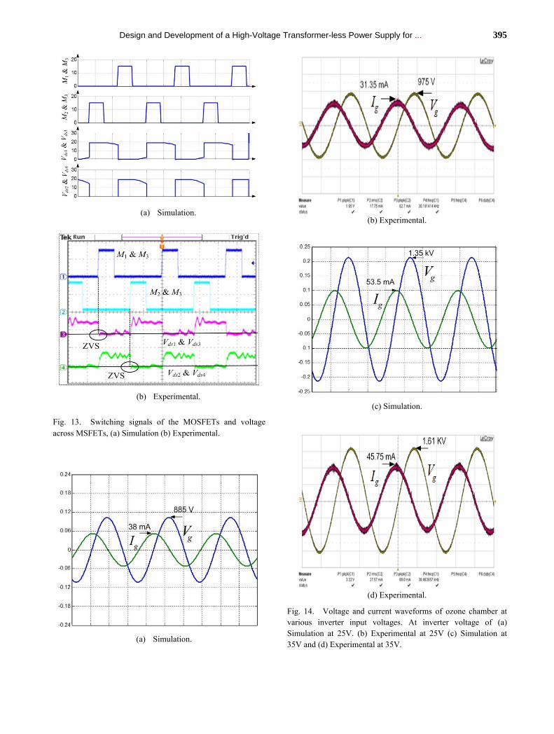
Fig. 14. Voltage and current waveforms of ozone chamber at various inverter input voltages. At inverter voltage of (a) Simulation at 25V. (b) Experimental at 25V (c) Simulation at 35V and (d) Experimental at 35V.

396 Journal of Power Electronics, Vol. 12, No. 3, May 2012
Fig. 16. Inverter input voltage versus the efficiency of the inverter.
Fig. 17. The efficiency comparison of transformer based and transformer-less power supply.
Fig. 15. Variation of ozone quantity with input voltage of inverter.
Fig. 13 shows the switching signals and the voltage across the switches. As can be seen, when power switches turn on, the voltage across each switch falls to zero. Consequently, no high voltage spikes occur during the turn off process. The maximum voltage that appears across power switches is equal to the inverter input voltage. Typically, high voltage spikes occur during turn off due to the leakage inductance of the transformer [20].
Fig. 14 illustrates the voltage and current waveforms of the ozone chamber. Clearly, the voltage and current waveforms are sinusoidal. The current leads the voltage because the switching frequency is fixed and the ozone generator behaves as a capacitive load. The effect of micro-discharges can be seen in the current waveforms. By increasing the voltage, the amplitude and duration of the micro-discharges increase in both cycles of the current waveform. As a result the ozone production increases.
In general, the simulation and experimental results are in good agreement, which confirms that the proposed model parameters are valid.
Fig. 15 shows the variation of the ozone quantity (mgO3/ Whr) with respect to the inverter input voltage. The ozone generator was fed with a 95% oxygen flow of 1 L/min. As can be seen, by increasing the input voltage, the ozone production increases. The input power is about 3.6 to 7 watts. The maximum ozone output is 20 mgO3/Whr. This ozone quantity is higher than the low power atmospheric pressure ozone generators reported in [8], [34].
Fig. 16 shows the overall efficiency of the inverter. To ensure the accuracy of the measured voltage and current, a high accuracy, high bandwidth LeCroy 600MHz oscilloscope is used. The maximum inverter efficiency is about 86%.
A comparison of efficiency of the proposed transformer-less power supply with that of other transformer based supplies is shown in Fig. 17. This comparison indicates
that the efficiency of the transformer-less power supply is greater than that of a ferrite core based transformer. However, it is less than that of a PT-based power supply. This is to be expected due to the non-winding nature of the PT. Despite this fact, the PT has several limitations as described in the introduction section.
VIII. CONCLUSION
In this paper, the development of an ozone generator without a transformer has been investigated. The advantages of the proposed system are its high efficiency, smaller footprint and lower cost. The voltage step-up is achieved only
by an Ls Cp resonant tank. By using muscovite mica as a dielectric material, ozone can be generated at about 1.5−3.5 kVp-p. Furthermore, ZCZVS operation is achieved by employing a 25% duty factor between the MOSFETs of the inverter bridge. To validate the viability of the proposed system, a prototype ozone generator is constructed. The

Design and Development of a High-Voltage Transformer-less Power Supply for ... 397
simulation and experimental results are found to be in close agreement with the theoretical predictions.
ACKNOWLEDGMENT
The authors would like to thank the Universiti Teknologi Malaysia for providing the facilities and research grant to conduct this research through vot. No 79411.
REFERENCES
[1] R. E. Araby, S. Hawash, and G. El Diwani, “Treatment of iron and manganese in simulated groundwater via ozone technology,” Desalination, Vol. 249, pp. 1345-1349, 2009.
[2] Evans and F. L, “Ozone in water and waste water treatment,” vol. Ann Arbor Science, 1975.
[3] U. Kogelschatz, and B. Eliasson, “Ozone generation and application, A Handbook of electrostatic processes,” New York :Marcel Dekker, chapter 26, pp. 581-606, 1995.
[4] C. Ordiz, J. M. Alonso, M. A. D. Costa, J. Ribas, and A. J. Calleja, “Development of a high-voltage closed-loop power supply for ozone generation,” in Proc. APEC, pp. 1861-1867, 2008.
[5] U. Kogelschatz, “Filamentary, patterned, and diffuse barrier discharges,” IEEE Trans. Plasma Science, Vol. 30, No. 4, pp. 1400-1408, Aug. 2002.
[6] J. M. Alonso, A. J. Calleja, J. Ribas, M. Rico-Secades, E. Corominas, J. Cardesin, and J. Garcia, “Low-power high-voltage universal-input inverter for ozone generation,” in Proc. CIEP, pp. 153-159, 2002.
[7] J. M. Alonso, A. J. Calleja, J. Ribas, M. Valdes, and J. Losada, “Analysis and design of a low-power high-voltage high-frequency power supply for ozone generation,” in Proc. IAS, pp. 2525-2532 , 2001.
[8] J. M. Alonso, J. Cardesin, E. L. Corominas, M. Rico-Secades, and J. Garcia, “Low-power high-voltage high-frequency power supply for ozone generation,” IEEE Trans. Ind. Appl., Vol. 40, No. 2, pp. 414-421, Mar. 2004.
[9] M. Ponce-Silva, J. Aguilar-Ramirez, E. Beutelspacher, J. M. Calderon, and C. Cortes, “Single-switch power supply based on the class E shunt amplifier for ozone generators,” in Proc. PESC, pp.1380-1385, 2007.
[10] O. Koudriavtsev, S. Wang, Y. Konishi, and M. Nakaoka, “A novel pulse-density-modulated high-frequency inverter for silent-discharge-type ozonizer,” IEEE Trans. Ind. Appl., , Vol. 38, No. 2, pp. 369-378, Mar. 2002.
[11] O. Koudriavtsev, W. Shengpei, and M. Nakaoka, “Advanced development of voltage source soft-switching high-frequency inverter for silent discharge tube loads,” in Proc. IPEMC, pp. 302-307, 2000.
[12] K. Jung and Y. Suh, “Medium Voltage Power Supply with Enhanced Ignition Characteristics for Plasma Torches,” Journal of Power Electronics, Vol. 11, No. 4, Jul. 2011.
[13] W. Shengpei, Y. Konishi, O. Koudriavtsev, and M. Nakaoka, “A novel silent discharge type ozonizer using pulse density modulated high-frequency inverter,” in Proc. IAS, pp. 764-772, 1999.
[14] P. Hothongkham and V. Kinnares, “Constant voltage control of high voltage high frequency power supply for ozone quantity adjustment,” in Proc. ISCAS, pp. 1977-1980 , 2009.
[15] P. Hothongkham and V. Kinnares, “High-voltage high-frequency power supply using a phase-shifted PWM full bridge inverter fed ozone generator with constant applied electrode voltage,” in Proc. IPEC, pp. 1560-1567, 2010.
[16] P. Hothongkham and V. Kinnares, “Measurement of an ozone generator using a phase-shifted PWM full bridge inverter,” in Proc. IPEC, pp. 1552-1559, 2010.
[17] V. Kinnares and P. Hothongkham, “Circuit analysis and modeling of a phase-shifted pulsewidth modulation full-bridge-inverter-fed ozone generator with constant applied electrode voltage,” IEEE Trans. Power Electron, Vol. 25, No. 7, pp. 1739-1752, Jul. 2010.
[18] J. M. Alonso, J. Cardesin, J. A. Martin-Ramos, J. Garcia, and M. Rico-Secades, “Using current-fed parallel-resonant inverters for electrodischarge applications: a case of study,” in Proc. APEC, pp. 109-115, 2004.
[19] A. Namadmalan, J. S. Moghani, and J. Milimonfared, “A current-fed parallel resonant push-pull inverter with a new cascaded coil flux control for induction heating applications,” Journal of Power Electronic, Vol. 11, No. 5, Sep. 2011.
[20] J. M. Alonso, J. Garcia, A. J. Calleja, J. Ribas, and J. Cardesin, “Analysis, design, and experimentation of a high-voltage power supply for ozone generation based on current-fed parallel-resonant push-pull inverter,” IEEE Trans. Ind. Appl., Vol. 41, No. 7, pp. 1364-1372, Sep. 2005.
[21] J. M. Alonso, C. Ordiz, M. A. D. Costa, J. Ribas, and J. Cardesin, “High voltage power supply for ozone generation based on piezoelectric transformer,” in Proc. IAS, pp. 1901-1908, 2007.
[22] J. M. Alonso, C. Ordiz, D. Gacio, J. Ribas, and A. J. Calleja, “Closed-loop regulated power supply for ozone generation based on buck converter and current-fed push-pull resonant inverter,” in Proc. EPE, pp. 1-10, 2009.
[23] J. M. Alonso, C. Ordiz, M. A. Dalla Costa, J. Ribas, and J. Cardesin, “High-voltage power supply for ozone generation based on piezoelectric transformer,” IEEE Trans. Ind. Appl., Vol. 45, No. 4, pp. 1513-1523, 2009.
[24] M. Facta, Z. Salam, and Z. Buntat, “The development of ozone generation with low power consumption,” in Proc. CITISIA, pp. 440-445, 2009.
[25] M. Facta, Z. Salam, A. Jusoh, and Z. Bin Buntat, “Improvement in ozone generation with low voltage high frequency power converters,” in Proc. PECON, pp. 1446-1450, 2008.
[26] M. Z. Youssef and P. K. Jain, “Modeling techniques of resonant converters: merits and demerits,” in Proc. ECE, pp. 241-244, 2004.
[27] D. C. Hamill, “Class DE inverters and rectifiers for DC-DC conversion,” in Proc. PESC, pp. 854-860, 1996.
[28] J. M. Alonso, M. Valdés, A. J. Calleja, J. Ribas, and J. Losada, “High frequency testing and modeling of silent discharge ozone generators,” Ozone: Science & Engineering: The Journal of the International Ozone Association, vol. 25, pp. 363 - 376, 2003.
[29] E. Akpinar and I. Yilmazlar, “Transformerless single phase inverter design for LCD television,” IEEE Trans. Consumer Electro., Vol. 53, No. 2, pp. 697-703, May 2007.
[30] M. C. Cosby Jr. and R. M. Nelms, “A resonant inverter for electronic ballast applications,” IEEE Trans. Ind. Electron., Vol. 41, No. 4, pp. 418-425, Aug. 1994.

398 Journal of Power Electronics, Vol. 12, No. 3, May 2012
[31] A. Bucher, T. Durbaum, D. Kubrich, and A. Stadler, “Comparison of different design methods for the parallel resonant converter,” in Proc. EPE-PEMC, pp. 810-815, 2006.
[32] M. Matsuo, H. Sekiya, T. Suetsugu, K. Shinoda, and S.
Mori, “Design of a high-efficiency class DE tuned power oscillator,” IEEE Trans. Circuits Syst. I, Fundam. Theory Appl., Vol. 47, No. 11, pp. 1645-1649, Nov. 2000.
[33] C. Wm and T. Mclyman, Transformer and Inductor Design Handbook, Third Edition Maracel Dekkar, Inc New York.
[34] S. Potivejkul, V. Kinnares, and P. Rattanavichien, “Design of ozone generator using solar energy,” in Proc. APCCAS, pp. 217-220, 1998.
Mochammad Facta received his B.S. in
Electrical Engineering from the Universitas
Hasanuddin, Makassar, Indonesia, and his
M.S. from Institut Teknologi 10 November,
Surabaya, Indonesia. He is a Lecturer at the
Universitas Diponegoro, Semarang,
Indonesia. He is currently pursuing his Ph.D. at the Universiti
Teknologi Malaysia, Johor, Malaysia.
Muhammad Amjad received his B.Sc. and
M.Sc. in Electrical Engineering from the
University of Engineering and Technology
(UET), Lahore, Pakistan, in 1998 and 2006,
respectively. He is currently working
towards his PhD in Electrical Engineering
from the Universiti Teknologi Malaysia (UTM), Johor, Malaysia.
He has been a Lecturer in the University College of Engineering
and Technology (UCET), The Islamia University of Bahawalpur
(IUB), Bahawalpur, Pakistan for 11 years. His research interests
include the modeling of dielectric barrier discharge (DBD)
chambers and power electronic converters for DBD applications.
Kashif Ishaque received his B.E. in
Industrial Electronics Engineering from the
Institute of Industrial Electronics
Engineering, NEDUET, Karachi, Pakistan, in
2007, and his M.E. in Mechatronics and
Automatic Control, in 2009, from the
Universiti Teknologi Malaysia (UTM), Johor, Malaysia, where
he is currently working toward his Ph.D. in Electrical
Engineering. He is an Assistant Professor at the PAF Karachi
Institute of Economics and Technology (PAF-KIET), Karachi,
Pakistan. His research interests include photovoltaic modelling
and control, intelligent control, nonlinear systems control and
optimization techniques such as genetic algorithms (GA),
particle swarm optimization (PSO) and differential evolutions
(DE).
Zainal Salam obtained his B.S., M.E.E. and
Ph.D. from the University of California, the
Universiti Teknologi Malaysia (UTM) and
the University of Birmingham, UK, in 1985,
1989 and 1997, respectively. He has been a
Lecturer at UTM for 25 years and is now a
Professor of Power Electronics in the Faculty of Electrical
Engineering. He has been working on several research and
consulting projects in the areas of battery powered converters,
solar energy and machine control. Currently he is the Director of
the Inverter Quality Control Center (IQCC) UTM which is
responsible for testing the PV inverters that are to be connected
to the local utility grid. His research interests include all areas of
instrumentation and control for renewable energy.